US8219940B2 - Method and apparatus for removing dummy features from a data structure - Google Patents
Method and apparatus for removing dummy features from a data structureDownload PDFInfo
- Publication number
- US8219940B2 US8219940B2US11/174,732US17473205AUS8219940B2US 8219940 B2US8219940 B2US 8219940B2US 17473205 AUS17473205 AUS 17473205AUS 8219940 B2US8219940 B2US 8219940B2
- Authority
- US
- United States
- Prior art keywords
- data structure
- source data
- dummy
- dummy features
- feature
- Prior art date
- Legal status (The legal status is an assumption and is not a legal conclusion. Google has not performed a legal analysis and makes no representation as to the accuracy of the status listed.)
- Active, expires
Links
Images


Classifications
- G—PHYSICS
- G06—COMPUTING OR CALCULATING; COUNTING
- G06F—ELECTRIC DIGITAL DATA PROCESSING
- G06F30/00—Computer-aided design [CAD]
- G06F30/30—Circuit design
- G06F30/39—Circuit design at the physical level
- G—PHYSICS
- G06—COMPUTING OR CALCULATING; COUNTING
- G06F—ELECTRIC DIGITAL DATA PROCESSING
- G06F18/00—Pattern recognition
- G06F18/20—Analysing
- G06F18/21—Design or setup of recognition systems or techniques; Extraction of features in feature space; Blind source separation
- G06F18/211—Selection of the most significant subset of features
- G06F18/2113—Selection of the most significant subset of features by ranking or filtering the set of features, e.g. using a measure of variance or of feature cross-correlation
Definitions
- data structures of the multiple layers of the VLSI devicemay be generated from the physical device to verify the circuit design or for the reverse-engineering extraction of the circuitry.
- These data structuresare normally constructed in a vector-based format, known commonly in the industry as GDSII.
- GDSIIvector-based format
- the dummy featuresif not removed from the generated data structure, add more complexity to signal tracing and/or analysis of the circuits; and reduce the clarity with which multiple layers may be seen when overlaid. Additionally they significantly increase the size of the already large vector-based data structures, without significantly adding function. When processing these data structures to recognize function, dummy features add needless processing time.
- the methodsimply compresses the data within the vector-based data structure but does not remove the non-functional elements.
- the non-functional elementsare still present in the data structure and needlessly increase its size and processing time.
- the lower metal layers of connectivityare obscured by the dummy features on the upper levels. This complicates signal tracing and analysis for an observer.
- the methoddoes not teach how to locate the non-functional elements within the data structure, and as such would not be useful in data structures other than GDSII format data structures.
- the present inventionis directed to a method and apparatus to reduce occurrences of electrically non-functional elements, known as dummy features, from a source data structure.
- the source data structuremay be image data provided by a high-resolution image acquisition system to image electronic circuits and embedded features of an integrated circuit (IC).
- the source data structuremay be vector based data provided in the industry standard GDSII format.
- dummy features in the source data structureare detected and then deleted from the source data structure.
- dummy features in a source data structureare detected by selecting a representative dummy feature pattern or polygon as a reference pattern or polygon, depending on the type of source data structure, and comparing the selected reference pattern or polygon to feature patterns or polygons in the source data structure.
- a dummy feature patternmay be selected by framing the dummy feature reference pattern by a pixel matrix of m ⁇ n pixels and selecting a cut-off correlation threshold value.
- a dummy feature polygonmay be selected by forming the dummy feature reference polygon by extracting points of interest from the dummy feature and then selecting a cut-off correlation threshold value.
- the step of comparing the selected reference pattern to feature patterns in the source data structurecomprises computing the correlation coefficients between the reference pattern and the feature patterns in the source data structure and comparing computed correlation coefficients to the selected cut-off correlation threshold value.
- the comparing of selected reference polygons to feature polygons in the source data structureincludes computing the correlation coefficients between points of interest in the feature polygons in the source data structure and the reference polygon.
- the computed correlation coefficientsmay be based on gray scale values or may be calculated using a sum of squared differences equation:
- I (i, j)is the image array
- Pis the reference pattern array
- SSD (i, j)is the correlation coefficient
- (i, j)are the coordinates in the image array.
- feature patterns or polygonsare selectively removed based on a comparison between their correlation coefficients and the selected cut-off correlation threshold value.
- a new threshold valuemay be selected to remove all dummy features in the source data structure or to prevent removal of non-dummy features.
- another reference pattern or polygonwill be selected and the process repeated. Once the identified dummy features have been deleted from the source data structure, another data structure may be loaded and the above process repeated.
- the source data structure with the removed dummy featuresmay be stored in a memory together with the selected dummy feature pattern or polygon and the last selected cut-off correlation threshold.
- FIG. 1is a block diagram depicting an embodiment of apparatus in accordance with the present invention
- FIG. 2is a basic flowchart representation of the present invention
- FIG. 3is a flowchart representation of an embodiment of a calibration stage of an embodiment of the present invention
- FIG. 4is a flowchart representation of another embodiment of a calibration stage of an embodiment of the present invention.
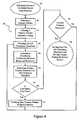
- the basic steps of the present inventionare summarized in the flowchart of FIG. 2 .
- the calibration stageincludes defining 14 the dummy feature pattern to be used as a reference and selecting 16 a correlation cut-off threshold.
- Correlation coefficients between the feature patterns in the source data structure and the reference patternare computed 18 using a correlation equation.
- the correlation coefficientsare then compared to the selected cut-off threshold coefficient. Feature patterns that have a correlation coefficient better than the threshold value are identified as the dummy features, which are removed 20 .
- a small portion of the entire source data structureis selected 30 for the calibration stage (an i ⁇ j matrix of pixels). This portion would be selected by the user based on the number of dummy features in the observed structure. The greater the number of dummy features the more useful the dummy feature calibration will be when moved to the deletion stage.
- a human operatorexamines the selected portion of the source data structure and selects 32 a dummy feature to be used as a reference pattern 14 . The user accomplishes this by selecting a pixel matrix of m ⁇ n pixels to frame the reference dummy feature pattern.
- the operatorselects 16 a starting correlation cut-off threshold value, alternatively the starting point may be auto-selected as a predetermined value.
- the systemthen examines a portion (a size corresponding to the m ⁇ n matrix of the reference pattern) of the calibration data structure, starting at an origin point. This is called a feature pattern. If the calibration data structure is an image file, then the gray-scale values from the dummy reference pattern are obtained and used to compute 18 the correlation coefficient. The system compares the gray-scale values of the dummy reference pattern to the gray-scale values of the feature pattern within the calibration data structure.
- a correlation coefficientmay be computed 18 , for example, as a sum of squared difference (SSD) correlation coefficient.
- SSDsum of squared difference
- the systemAfter the comparison is made, the system iterates the coordinates of the feature pattern to compare the next portion of the calibration data structure. This continues until the system has calculated the correlation coefficients for the entire calibration data structure.
- Removalmeans the deletion of the feature from the source data structure, what remains is the background information of the source data structure. In the case of image data this means the replacement of the pixel space occupied by the feature, with pixel data corresponding to background. Information indicating the former presence of a dummy feature will not be available.
- a human operatorexamines the calibration area file to determine if all the dummy features have been removed 34 using the selected 16 cut-off correlation threshold.
- the operatormay update the cut-off correlation threshold by selecting 16 a new value for the cut-off threshold value if an insufficient number of dummy features were removed. If there are dummy features remaining, the operator may choose to lower 16 the correlation cut-off threshold value. Also, if the operator finds that features that are not dummy-features have been removed, the operator may choose to raise 16 the correlation cut-off threshold value. For example, an exact match between the reference pattern 14 and a pattern of interest would require the values for both the defined 14 reference pattern and the pattern of interest to be identical. Due to the non-uniform illumination and noise in an image-based data-structure, the gray-scale levels on identical dummy feature patterns will vary slightly. A more realistic cut-off correlation threshold value may be selected 16 , permitting a slight variance between patterns.
- gray-scale datawould not be available, but alternate data could be used for comparison.
- One skilled in the artwould be able to examine the vector-based data structure to extract points of interest from the dummy feature to form a reference polygon. These points of interest could be compared to the feature polygons in the data-structure, which would enable a similar correlation comparison made for the gray-scale data.
- a correlation thresholdcould be set for correlation between points of interest in the reference polygon as compared to the feature polygon, identifying the dummy features for removal.
- one skilled in the artwould be able to create a labeled pixel data structure from the GDSII information, wherein the pixel values would correspond to whether or not the pixel was part of the background, a metal line, or a via.
- gray-scale datacould be substituted by other types of data upon which a correlation could be made without departing from the scope of the invention.
- correlation methodscould also be used depending on the format of the source data structure, the other methods for example could include, FFT (Fast Fourier Transform), geometric hashing or feature-based algorithms. It should also be noted that the steps of determining the presence of dummy features and adjusting the cut-off threshold may also be performed algorithmically without departing from the scope of the invention.
- the remaining dummy featuresare detected using the newly updated threshold value.
- This updating step 34may be repeated several times until a sufficient number of dummy features have been detected and deleted. Once this is done, the “best fit” cut-off selected 16 threshold value, that is, the last threshold value computed and the defined 14 reference dummy feature pattern are stored 38 in memory.
- a usermay find that the selected dummy feature reference pattern is not the best example of the dummy feature pattern in the source data structure. If an operator discovers a poor correlation between the reference pattern and the feature patterns; one may chose a new dummy feature pattern as a better representation.
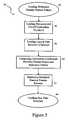
- FIG. 4is a flow chart representation of another embodiment of the calibration stage. The user defines 40 a calibration portion of the source data structure to examine. The user then selects 42 a dummy feature and defines 14 the dummy feature reference pattern by selecting an m ⁇ n matrix of pixels that frames the dummy feature pattern. The user then selects 16 an initial cut-off correlation threshold value. The system then calculates 18 the correlation between the reference pattern and the feature patterns.
Landscapes
- Engineering & Computer Science (AREA)
- Theoretical Computer Science (AREA)
- Physics & Mathematics (AREA)
- Data Mining & Analysis (AREA)
- Computer Hardware Design (AREA)
- Evolutionary Computation (AREA)
- General Engineering & Computer Science (AREA)
- General Physics & Mathematics (AREA)
- Geometry (AREA)
- Life Sciences & Earth Sciences (AREA)
- Artificial Intelligence (AREA)
- Bioinformatics & Cheminformatics (AREA)
- Bioinformatics & Computational Biology (AREA)
- Computer Vision & Pattern Recognition (AREA)
- Evolutionary Biology (AREA)
- Image Processing (AREA)
- Image Analysis (AREA)
- Design And Manufacture Of Integrated Circuits (AREA)
Abstract
Description
where:
I (i, j) is the image array;
P is the reference pattern array;
SSD (i, j) is the correlation coefficient,
(i, j) are the coordinates in the image array.
where:
I (i+k,j+c) is the source image array;
P (k,c) is the reference pattern array;
SSD (i,j) is the correlation coefficient for all (i,j);
(i,j) are the pixel coordinates in the source image array;
k is an integer value ranging from 1 to n; and
c is an integer value ranging from 1 to m.
Claims (32)
Priority Applications (3)
| Application Number | Priority Date | Filing Date | Title |
|---|---|---|---|
| US11/174,732US8219940B2 (en) | 2005-07-06 | 2005-07-06 | Method and apparatus for removing dummy features from a data structure |
| US11/976,409US7765517B2 (en) | 2005-07-06 | 2007-10-24 | Method and apparatus for removing dummy features from a data structure |
| US12/816,144US7886258B2 (en) | 2005-07-06 | 2010-06-15 | Method and apparatus for removing dummy features from a data structure |
Applications Claiming Priority (1)
| Application Number | Priority Date | Filing Date | Title |
|---|---|---|---|
| US11/174,732US8219940B2 (en) | 2005-07-06 | 2005-07-06 | Method and apparatus for removing dummy features from a data structure |
Related Child Applications (1)
| Application Number | Title | Priority Date | Filing Date |
|---|---|---|---|
| US11/976,409DivisionUS7765517B2 (en) | 2005-07-06 | 2007-10-24 | Method and apparatus for removing dummy features from a data structure |
Publications (2)
| Publication Number | Publication Date |
|---|---|
| US20070011628A1 US20070011628A1 (en) | 2007-01-11 |
| US8219940B2true US8219940B2 (en) | 2012-07-10 |
Family
ID=37619674
Family Applications (3)
| Application Number | Title | Priority Date | Filing Date |
|---|---|---|---|
| US11/174,732Active2029-06-21US8219940B2 (en) | 2005-07-06 | 2005-07-06 | Method and apparatus for removing dummy features from a data structure |
| US11/976,409Active2026-02-27US7765517B2 (en) | 2005-07-06 | 2007-10-24 | Method and apparatus for removing dummy features from a data structure |
| US12/816,144Expired - LifetimeUS7886258B2 (en) | 2005-07-06 | 2010-06-15 | Method and apparatus for removing dummy features from a data structure |
Family Applications After (2)
| Application Number | Title | Priority Date | Filing Date |
|---|---|---|---|
| US11/976,409Active2026-02-27US7765517B2 (en) | 2005-07-06 | 2007-10-24 | Method and apparatus for removing dummy features from a data structure |
| US12/816,144Expired - LifetimeUS7886258B2 (en) | 2005-07-06 | 2010-06-15 | Method and apparatus for removing dummy features from a data structure |
Country Status (1)
| Country | Link |
|---|---|
| US (3) | US8219940B2 (en) |
Cited By (1)
| Publication number | Priority date | Publication date | Assignee | Title |
|---|---|---|---|---|
| US20100325593A1 (en)* | 2009-06-18 | 2010-12-23 | Zavadsky Vyacheslav L | Integrated circuit analysis systems and methods |
Families Citing this family (21)
| Publication number | Priority date | Publication date | Assignee | Title |
|---|---|---|---|---|
| US8219940B2 (en)* | 2005-07-06 | 2012-07-10 | Semiconductor Insights Inc. | Method and apparatus for removing dummy features from a data structure |
| US7570796B2 (en) | 2005-11-18 | 2009-08-04 | Kla-Tencor Technologies Corp. | Methods and systems for utilizing design data in combination with inspection data |
| EP2110697B1 (en) | 2008-04-17 | 2016-02-10 | Ruprecht-Karls-Universität Heidelberg | Wave field microscope with sub-wavelength resolution and methods for processing microscopic images to detect objects with sub-wavelength dimensions |
| US8155409B2 (en)* | 2008-04-17 | 2012-04-10 | Ruprecht-Karls-Universitat | Wave field microscope with sub-wavelength resolution and methods for processing microscopic images to detect objects with sub-wavelength dimensions |
| US9659670B2 (en) | 2008-07-28 | 2017-05-23 | Kla-Tencor Corp. | Computer-implemented methods, computer-readable media, and systems for classifying defects detected in a memory device area on a wafer |
| US8775101B2 (en) | 2009-02-13 | 2014-07-08 | Kla-Tencor Corp. | Detecting defects on a wafer |
| US8781781B2 (en) | 2010-07-30 | 2014-07-15 | Kla-Tencor Corp. | Dynamic care areas |
| US9170211B2 (en) | 2011-03-25 | 2015-10-27 | Kla-Tencor Corp. | Design-based inspection using repeating structures |
| US9087367B2 (en) | 2011-09-13 | 2015-07-21 | Kla-Tencor Corp. | Determining design coordinates for wafer defects |
| US8831334B2 (en) | 2012-01-20 | 2014-09-09 | Kla-Tencor Corp. | Segmentation for wafer inspection |
| US8826200B2 (en)* | 2012-05-25 | 2014-09-02 | Kla-Tencor Corp. | Alteration for wafer inspection |
| US9189844B2 (en) | 2012-10-15 | 2015-11-17 | Kla-Tencor Corp. | Detecting defects on a wafer using defect-specific information |
| US8806392B2 (en)* | 2012-12-03 | 2014-08-12 | Taiwan Semiconductor Manufacturing Company, Ltd. | Distinguishable IC patterns with encoded information |
| US9053527B2 (en) | 2013-01-02 | 2015-06-09 | Kla-Tencor Corp. | Detecting defects on a wafer |
| US9134254B2 (en) | 2013-01-07 | 2015-09-15 | Kla-Tencor Corp. | Determining a position of inspection system output in design data space |
| US9311698B2 (en) | 2013-01-09 | 2016-04-12 | Kla-Tencor Corp. | Detecting defects on a wafer using template image matching |
| KR102019534B1 (en) | 2013-02-01 | 2019-09-09 | 케이엘에이 코포레이션 | Detecting defects on a wafer using defect-specific and multi-channel information |
| US9865512B2 (en) | 2013-04-08 | 2018-01-09 | Kla-Tencor Corp. | Dynamic design attributes for wafer inspection |
| US9310320B2 (en) | 2013-04-15 | 2016-04-12 | Kla-Tencor Corp. | Based sampling and binning for yield critical defects |
| US9075948B2 (en)* | 2013-07-31 | 2015-07-07 | International Business Machines Corporation | Method of improving timing critical cells for physical design in the presence of local placement congestion |
| US12437237B2 (en)* | 2022-07-07 | 2025-10-07 | Capital One Services, Llc | Sequential synthesis and selection for feature engineering |
Citations (86)
| Publication number | Priority date | Publication date | Assignee | Title |
|---|---|---|---|---|
| US3909602A (en)* | 1973-09-27 | 1975-09-30 | California Inst Of Techn | Automatic visual inspection system for microelectronics |
| US4805123A (en)* | 1986-07-14 | 1989-02-14 | Kla Instruments Corporation | Automatic photomask and reticle inspection method and apparatus including improved defect detector and alignment sub-systems |
| US5060282A (en)* | 1990-03-26 | 1991-10-22 | The United States Of America As Represented By The United States Department Of Energy | Optical pattern recognition architecture implementing the mean-square error correlation algorithm |
| US5060284A (en) | 1990-03-23 | 1991-10-22 | Eastman Kodak Company | Adaptive error diffusion thresholding for document images |
| US5138672A (en)* | 1988-12-08 | 1992-08-11 | Canon Kabushiki Kaisha | Image reducing apparatus |
| US5287856A (en)* | 1991-04-26 | 1994-02-22 | Dornier Medizintechnik Gmbh | Focal range locating system for lithotrity |
| US5361311A (en)* | 1992-07-14 | 1994-11-01 | The United States Of America As Represented By The Secretary Of Commerce | Automated recongition of characters using optical filtering with positive and negative functions encoding pattern and relevance information |
| US5481625A (en)* | 1992-04-15 | 1996-01-02 | Pioneer Electronic Corporation | Handwritten character recognition device |
| US5544256A (en)* | 1993-10-22 | 1996-08-06 | International Business Machines Corporation | Automated defect classification system |
| US5548326A (en)* | 1993-10-06 | 1996-08-20 | Cognex Corporation | Efficient image registration |
| US5550936A (en)* | 1991-08-23 | 1996-08-27 | Mitsubishi Denki Kabushiki Kaisha | Image processing system |
| US5608816A (en)* | 1993-12-24 | 1997-03-04 | Matsushita Electric Industrial Co., Ltd. | Apparatus for inspecting a wiring pattern according to a micro-inspection and a macro-inspection performed in parallel |
| US5613013A (en) | 1994-05-13 | 1997-03-18 | Reticula Corporation | Glass patterns in image alignment and analysis |
| US5640200A (en)* | 1994-08-31 | 1997-06-17 | Cognex Corporation | Golden template comparison using efficient image registration |
| US5781656A (en)* | 1994-03-18 | 1998-07-14 | Fujitsu Limited | Method and apparatus for inspecting patterns composed of reticle data |
| US5861910A (en)* | 1996-04-02 | 1999-01-19 | Mcgarry; E. John | Image formation apparatus for viewing indicia on a planar specular substrate |
| US5887080A (en)* | 1994-01-28 | 1999-03-23 | Kabushiki Kaisha Toshiba | Method and apparatus for processing pattern image data by SEM |
| US5917953A (en)* | 1997-07-07 | 1999-06-29 | The Morgan Crucible Company Plc | Geometry implicit sampler for polynomial surfaces over freeform two-dimensional domains |
| US5933522A (en)* | 1996-09-11 | 1999-08-03 | Nec Corporation | Specific part searching method and device for memory LSI |
| US6005985A (en) | 1997-07-29 | 1999-12-21 | Lockheed Martin Corporation | Post-processing system for optical correlators |
| US6047084A (en)* | 1997-11-18 | 2000-04-04 | Motorola, Inc. | Method for determining accuracy of a circuit assembly process and machine employing the same |
| US6075905A (en)* | 1996-07-17 | 2000-06-13 | Sarnoff Corporation | Method and apparatus for mosaic image construction |
| US6088483A (en)* | 1997-07-02 | 2000-07-11 | International Business Machines Corporation | Image processing method for system employing pattern matching |
| US6236746B1 (en)* | 1996-10-01 | 2001-05-22 | Semiconductor Insights, Inc. | Method to extract circuit information |
| US6290572B1 (en)* | 2000-03-23 | 2001-09-18 | Micron Technology, Inc. | Devices and methods for in-situ control of mechanical or chemical-mechanical planarization of microelectronic-device substrate assemblies |
| US6295374B1 (en) | 1998-04-06 | 2001-09-25 | Integral Vision, Inc. | Method and system for detecting a flaw in a sample image |
| US6305000B1 (en)* | 1999-06-15 | 2001-10-16 | International Business Machines Corporation | Placement of conductive stripes in electronic circuits to satisfy metal density requirements |
| US6333141B1 (en)* | 1998-07-08 | 2001-12-25 | International Business Machines Corporation | Process for manufacture of integrated circuit device using inorganic/organic matrix comprising polymers of three dimensional architecture |
| US20020144224A1 (en)* | 2001-04-02 | 2002-10-03 | Martin Frerichs | Method for calculating the capacity of a layout of an integrated circuit with the aid of a computer, and application of the method to integrated circuit fabrication |
| US6473536B1 (en)* | 1998-09-18 | 2002-10-29 | Sanyo Electric Co., Ltd. | Image synthesis method, image synthesizer, and recording medium on which image synthesis program is recorded |
| US6477685B1 (en)* | 1999-09-22 | 2002-11-05 | Texas Instruments Incorporated | Method and apparatus for yield and failure analysis in the manufacturing of semiconductors |
| US20030035592A1 (en)* | 2000-09-08 | 2003-02-20 | Cornog Katherine H. | Interpolation of a sequence of images using motion analysis |
| US20030044059A1 (en)* | 2001-08-28 | 2003-03-06 | Numerical Technologies, Inc. | System and method for indentifying dummy features on a mask layer |
| US20030073010A1 (en)* | 2001-10-16 | 2003-04-17 | Dai Nippon Print. Co., Ltd. | Photomask inspecting method |
| US20030076361A1 (en) | 2001-09-12 | 2003-04-24 | Haruo Hatanaka | Image synthesizer, image synthesis method and computer readable recording medium having image synthesis processing program recorded thereon |
| US6567949B2 (en)* | 1998-05-29 | 2003-05-20 | Siemens Aktiengesellschaft | Method and configuration for error masking |
| US6581193B1 (en)* | 2001-06-13 | 2003-06-17 | Kla-Tencor | Apparatus and methods for modeling process effects and imaging effects in scanning electron microscopy |
| US6587579B1 (en)* | 2000-01-26 | 2003-07-01 | Agilent Technologies Inc. | Feature quality in array fabrication |
| US6594801B1 (en)* | 2000-11-03 | 2003-07-15 | Motorola, Inc. | Method for compressing a data structure representing a layout of a VLSI device |
| US6609235B2 (en)* | 2001-06-22 | 2003-08-19 | Bae Systems Information And Electronic Systems Integration, Inc. | Method for providing a fill pattern for an integrated circuit design |
| US6658145B1 (en)* | 1997-12-31 | 2003-12-02 | Cognex Corporation | Fast high-accuracy multi-dimensional pattern inspection |
| US20030226757A1 (en)* | 2002-06-07 | 2003-12-11 | Smith Taber H. | Dummy fill for integrated circuits |
| US6674890B2 (en) | 1997-10-29 | 2004-01-06 | Hitachi, Ltd. | Defect inspection method and apparatus therefor |
| US6691052B1 (en)* | 2002-01-30 | 2004-02-10 | Kla-Tencor Corporation | Apparatus and methods for generating an inspection reference pattern |
| US6706456B2 (en)* | 2000-10-05 | 2004-03-16 | Nikon Corporation | Method of determining exposure conditions, exposure method, device manufacturing method, and storage medium |
| US6731991B1 (en)* | 1999-07-19 | 2004-05-04 | Laser Force, Inc. | System for projecting light on a work surface to produce an image for tracing |
| US20040098674A1 (en)* | 2002-11-19 | 2004-05-20 | Cadence Design Systems, Inc. | Place and route tool that incorporates a metal-fill mechanism |
| US6751343B1 (en)* | 1999-09-20 | 2004-06-15 | Ut-Battelle, Llc | Method for indexing and retrieving manufacturing-specific digital imagery based on image content |
| US20040151392A1 (en)* | 2003-02-04 | 2004-08-05 | Semiconductor Technology Academic Research Center | Image encoding of moving pictures |
| US20040170326A1 (en)* | 2003-01-27 | 2004-09-02 | Tomonori Kataoka | Image-processing method and image processor |
| US20040234135A1 (en)* | 2002-02-22 | 2004-11-25 | Yasuyuki Nomizu | Image data processing apparatus for and image data processing method of pattern matching |
| US6870951B2 (en)* | 2002-02-13 | 2005-03-22 | Numerical Technologies, Inc. | Method and apparatus to facilitate auto-alignment of images for defect inspection and defect analysis |
| US20050096887A1 (en) | 2003-10-31 | 2005-05-05 | International Business Machines Corporation | Techniques for reconstructing synthetic networks using pair-wise correlation analysis |
| US6901574B2 (en)* | 2001-02-09 | 2005-05-31 | Lacour Patrick J. | Data management method for mask writing |
| US20050129305A1 (en)* | 1999-08-25 | 2005-06-16 | Eastman Kodak Company | Method for forming a depth image |
| US20050132306A1 (en)* | 2002-06-07 | 2005-06-16 | Praesagus, Inc., A Massachusetts Corporation | Characterization and reduction of variation for integrated circuits |
| US6930782B1 (en)* | 2003-03-28 | 2005-08-16 | Lam Research Corporation | End point detection with imaging matching in semiconductor processing |
| US20050251771A1 (en)* | 2004-05-07 | 2005-11-10 | Mentor Graphics Corporation | Integrated circuit layout design methodology with process variation bands |
| US6969762B2 (en)* | 2003-10-31 | 2005-11-29 | Allegheny-Singer Research Institute | Selected nucleotide sequences isolated from pathogenic strains of Haemophilus influenzae |
| US20050271264A1 (en)* | 2004-04-21 | 2005-12-08 | Topcon Corporation | Three-dimensional image measuring apparatus and method |
| US6975755B1 (en)* | 1999-11-25 | 2005-12-13 | Canon Kabushiki Kaisha | Image processing method and apparatus |
| US20050286755A1 (en)* | 2004-06-25 | 2005-12-29 | Fereydoun Maali | Photomask image registration in scanning electron microscope imagery |
| US7003758B2 (en)* | 2003-10-07 | 2006-02-21 | Brion Technologies, Inc. | System and method for lithography simulation |
| US20060045325A1 (en)* | 2004-08-31 | 2006-03-02 | Semiconductor Insights Inc. | Method of design analysis of existing integrated circuits |
| US20060050953A1 (en)* | 2004-06-18 | 2006-03-09 | Farmer Michael E | Pattern recognition method and apparatus for feature selection and object classification |
| US20060059452A1 (en)* | 2004-08-27 | 2006-03-16 | Whitefield Bruce J | Pattern component analysis and manipulation |
| US7016539B1 (en)* | 1998-07-13 | 2006-03-21 | Cognex Corporation | Method for fast, robust, multi-dimensional pattern recognition |
| US7020866B2 (en)* | 2002-09-24 | 2006-03-28 | Renesas Technology Corp. | Mask data processor |
| US20060098893A1 (en)* | 2003-02-13 | 2006-05-11 | Sony Corporation | Signal processing device, method, and program |
| US20060104103A1 (en)* | 2002-12-20 | 2006-05-18 | Thales | Method for optical authentication and identification of objects and device therefor |
| US7075704B2 (en)* | 2003-03-19 | 2006-07-11 | Seiko Epson Corporation | Test-element-provided substrate, method of manufacturing the same, substrate for electro-optical device, electro-optical device, and electronic apparatus |
| US20060161403A1 (en) | 2002-12-10 | 2006-07-20 | Jiang Eric P | Method and system for analyzing data and creating predictive models |
| US20060245631A1 (en)* | 2005-01-27 | 2006-11-02 | Richard Levenson | Classifying image features |
| US20070062284A1 (en)* | 2005-09-22 | 2007-03-22 | Akihiro Machida | Image-based sensing of acceleration |
| US7206443B1 (en)* | 1999-08-05 | 2007-04-17 | Orbotech Ltd. | Apparatus and methods for the inspection of objects |
| US7236643B2 (en)* | 2002-03-22 | 2007-06-26 | Lockheed Martin Corporation | System and method for filtering and binarization of images in the presence of specular noise |
| US7239738B2 (en)* | 2002-09-13 | 2007-07-03 | Fuji Xerox Co., Ltd. | Image defect inspecting apparatus and image defect inspecting method |
| US7242095B2 (en)* | 2003-03-13 | 2007-07-10 | Fujitsu Limited | Semiconductor device having a dummy pattern |
| US7278121B2 (en)* | 2004-08-23 | 2007-10-02 | Semiconductor Insights Inc. | Method and apparatus for reducing redundant data in a layout data structure |
| US20070256039A1 (en)* | 2002-06-07 | 2007-11-01 | Cadence Design Systems, Inc. | Dummy fill for integrated circuits |
| US20080059920A1 (en)* | 2005-07-06 | 2008-03-06 | Semiconductor Insights Inc. | Method and apparatus for removing dummy features from a data structure |
| US7363099B2 (en)* | 2002-06-07 | 2008-04-22 | Cadence Design Systems, Inc. | Integrated circuit metrology |
| US7409260B2 (en)* | 2005-08-22 | 2008-08-05 | Applied Materials, Inc. | Substrate thickness measuring during polishing |
| US7412676B2 (en)* | 2000-06-13 | 2008-08-12 | Nicolas B Cobb | Integrated OPC verification tool |
| US7433508B2 (en)* | 2003-03-12 | 2008-10-07 | Hitachi High-Technologies Corporation | Pattern inspection method and its apparatus |
| US7448010B1 (en)* | 2003-08-01 | 2008-11-04 | Cadence Design Systems, Inc. | Methods and mechanisms for implementing virtual metal fill |
Family Cites Families (5)
| Publication number | Priority date | Publication date | Assignee | Title |
|---|---|---|---|---|
| KR100457808B1 (en)* | 2002-01-18 | 2004-11-18 | 주식회사 파이어앤텍 | Environment-friendly neuter loaded stream extinguishant for general fire and method for preparing the same |
| US7136518B2 (en)* | 2003-04-18 | 2006-11-14 | Medispectra, Inc. | Methods and apparatus for displaying diagnostic data |
| JP3703799B2 (en)* | 2002-12-13 | 2005-10-05 | 沖電気工業株式会社 | Remaining film thickness distribution estimation method, patterning mask and insulating film removal mask correction method using residual film thickness distribution estimation method, and semiconductor element using modified patterning mask and insulating film removal mask Manufacturing method |
| CN100470375C (en)* | 2002-12-16 | 2009-03-18 | Asml荷兰有限公司 | Photolithography apparatus and device manufacturing method |
| WO2007005636A2 (en)* | 2005-06-30 | 2007-01-11 | Controlled Semiconductor, Inc. | Semiconductor failure analysis tool |
- 2005
- 2005-07-06USUS11/174,732patent/US8219940B2/enactiveActive
- 2007
- 2007-10-24USUS11/976,409patent/US7765517B2/enactiveActive
- 2010
- 2010-06-15USUS12/816,144patent/US7886258B2/ennot_activeExpired - Lifetime
Patent Citations (93)
| Publication number | Priority date | Publication date | Assignee | Title |
|---|---|---|---|---|
| US3909602A (en)* | 1973-09-27 | 1975-09-30 | California Inst Of Techn | Automatic visual inspection system for microelectronics |
| US4805123B1 (en)* | 1986-07-14 | 1998-10-13 | Kla Instr Corp | Automatic photomask and reticle inspection method and apparatus including improved defect detector and alignment sub-systems |
| US4805123A (en)* | 1986-07-14 | 1989-02-14 | Kla Instruments Corporation | Automatic photomask and reticle inspection method and apparatus including improved defect detector and alignment sub-systems |
| US5138672A (en)* | 1988-12-08 | 1992-08-11 | Canon Kabushiki Kaisha | Image reducing apparatus |
| US5060284A (en) | 1990-03-23 | 1991-10-22 | Eastman Kodak Company | Adaptive error diffusion thresholding for document images |
| US5060282A (en)* | 1990-03-26 | 1991-10-22 | The United States Of America As Represented By The United States Department Of Energy | Optical pattern recognition architecture implementing the mean-square error correlation algorithm |
| US5287856A (en)* | 1991-04-26 | 1994-02-22 | Dornier Medizintechnik Gmbh | Focal range locating system for lithotrity |
| US5550936A (en)* | 1991-08-23 | 1996-08-27 | Mitsubishi Denki Kabushiki Kaisha | Image processing system |
| US5481625A (en)* | 1992-04-15 | 1996-01-02 | Pioneer Electronic Corporation | Handwritten character recognition device |
| US5361311A (en)* | 1992-07-14 | 1994-11-01 | The United States Of America As Represented By The Secretary Of Commerce | Automated recongition of characters using optical filtering with positive and negative functions encoding pattern and relevance information |
| US5548326A (en)* | 1993-10-06 | 1996-08-20 | Cognex Corporation | Efficient image registration |
| US5544256A (en)* | 1993-10-22 | 1996-08-06 | International Business Machines Corporation | Automated defect classification system |
| US5608816A (en)* | 1993-12-24 | 1997-03-04 | Matsushita Electric Industrial Co., Ltd. | Apparatus for inspecting a wiring pattern according to a micro-inspection and a macro-inspection performed in parallel |
| US5887080A (en)* | 1994-01-28 | 1999-03-23 | Kabushiki Kaisha Toshiba | Method and apparatus for processing pattern image data by SEM |
| US5781656A (en)* | 1994-03-18 | 1998-07-14 | Fujitsu Limited | Method and apparatus for inspecting patterns composed of reticle data |
| US5613013A (en) | 1994-05-13 | 1997-03-18 | Reticula Corporation | Glass patterns in image alignment and analysis |
| US5640200A (en)* | 1994-08-31 | 1997-06-17 | Cognex Corporation | Golden template comparison using efficient image registration |
| US5861910A (en)* | 1996-04-02 | 1999-01-19 | Mcgarry; E. John | Image formation apparatus for viewing indicia on a planar specular substrate |
| US6075905A (en)* | 1996-07-17 | 2000-06-13 | Sarnoff Corporation | Method and apparatus for mosaic image construction |
| US5933522A (en)* | 1996-09-11 | 1999-08-03 | Nec Corporation | Specific part searching method and device for memory LSI |
| US6236746B1 (en)* | 1996-10-01 | 2001-05-22 | Semiconductor Insights, Inc. | Method to extract circuit information |
| US6088483A (en)* | 1997-07-02 | 2000-07-11 | International Business Machines Corporation | Image processing method for system employing pattern matching |
| US5917953A (en)* | 1997-07-07 | 1999-06-29 | The Morgan Crucible Company Plc | Geometry implicit sampler for polynomial surfaces over freeform two-dimensional domains |
| US6005985A (en) | 1997-07-29 | 1999-12-21 | Lockheed Martin Corporation | Post-processing system for optical correlators |
| US6674890B2 (en) | 1997-10-29 | 2004-01-06 | Hitachi, Ltd. | Defect inspection method and apparatus therefor |
| US6047084A (en)* | 1997-11-18 | 2000-04-04 | Motorola, Inc. | Method for determining accuracy of a circuit assembly process and machine employing the same |
| US6658145B1 (en)* | 1997-12-31 | 2003-12-02 | Cognex Corporation | Fast high-accuracy multi-dimensional pattern inspection |
| US6295374B1 (en) | 1998-04-06 | 2001-09-25 | Integral Vision, Inc. | Method and system for detecting a flaw in a sample image |
| US6567949B2 (en)* | 1998-05-29 | 2003-05-20 | Siemens Aktiengesellschaft | Method and configuration for error masking |
| US6333141B1 (en)* | 1998-07-08 | 2001-12-25 | International Business Machines Corporation | Process for manufacture of integrated circuit device using inorganic/organic matrix comprising polymers of three dimensional architecture |
| US7016539B1 (en)* | 1998-07-13 | 2006-03-21 | Cognex Corporation | Method for fast, robust, multi-dimensional pattern recognition |
| US6473536B1 (en)* | 1998-09-18 | 2002-10-29 | Sanyo Electric Co., Ltd. | Image synthesis method, image synthesizer, and recording medium on which image synthesis program is recorded |
| US6305000B1 (en)* | 1999-06-15 | 2001-10-16 | International Business Machines Corporation | Placement of conductive stripes in electronic circuits to satisfy metal density requirements |
| US6731991B1 (en)* | 1999-07-19 | 2004-05-04 | Laser Force, Inc. | System for projecting light on a work surface to produce an image for tracing |
| US7206443B1 (en)* | 1999-08-05 | 2007-04-17 | Orbotech Ltd. | Apparatus and methods for the inspection of objects |
| US20050129305A1 (en)* | 1999-08-25 | 2005-06-16 | Eastman Kodak Company | Method for forming a depth image |
| US6751343B1 (en)* | 1999-09-20 | 2004-06-15 | Ut-Battelle, Llc | Method for indexing and retrieving manufacturing-specific digital imagery based on image content |
| US6477685B1 (en)* | 1999-09-22 | 2002-11-05 | Texas Instruments Incorporated | Method and apparatus for yield and failure analysis in the manufacturing of semiconductors |
| US6975755B1 (en)* | 1999-11-25 | 2005-12-13 | Canon Kabushiki Kaisha | Image processing method and apparatus |
| US6587579B1 (en)* | 2000-01-26 | 2003-07-01 | Agilent Technologies Inc. | Feature quality in array fabrication |
| US6290572B1 (en)* | 2000-03-23 | 2001-09-18 | Micron Technology, Inc. | Devices and methods for in-situ control of mechanical or chemical-mechanical planarization of microelectronic-device substrate assemblies |
| US7412676B2 (en)* | 2000-06-13 | 2008-08-12 | Nicolas B Cobb | Integrated OPC verification tool |
| US20030035592A1 (en)* | 2000-09-08 | 2003-02-20 | Cornog Katherine H. | Interpolation of a sequence of images using motion analysis |
| US6706456B2 (en)* | 2000-10-05 | 2004-03-16 | Nikon Corporation | Method of determining exposure conditions, exposure method, device manufacturing method, and storage medium |
| US6594801B1 (en)* | 2000-11-03 | 2003-07-15 | Motorola, Inc. | Method for compressing a data structure representing a layout of a VLSI device |
| US6901574B2 (en)* | 2001-02-09 | 2005-05-31 | Lacour Patrick J. | Data management method for mask writing |
| US6865727B2 (en)* | 2001-04-02 | 2005-03-08 | Infineon Technologies Ag | Method for calculating the capacity of a layout of an integrated circuit with the aid of a computer, and application of the method to integrated circuit fabrication |
| US20020144224A1 (en)* | 2001-04-02 | 2002-10-03 | Martin Frerichs | Method for calculating the capacity of a layout of an integrated circuit with the aid of a computer, and application of the method to integrated circuit fabrication |
| US6581193B1 (en)* | 2001-06-13 | 2003-06-17 | Kla-Tencor | Apparatus and methods for modeling process effects and imaging effects in scanning electron microscopy |
| US6609235B2 (en)* | 2001-06-22 | 2003-08-19 | Bae Systems Information And Electronic Systems Integration, Inc. | Method for providing a fill pattern for an integrated circuit design |
| US20030044059A1 (en)* | 2001-08-28 | 2003-03-06 | Numerical Technologies, Inc. | System and method for indentifying dummy features on a mask layer |
| US7014955B2 (en)* | 2001-08-28 | 2006-03-21 | Synopsys, Inc. | System and method for indentifying dummy features on a mask layer |
| US20030076361A1 (en) | 2001-09-12 | 2003-04-24 | Haruo Hatanaka | Image synthesizer, image synthesis method and computer readable recording medium having image synthesis processing program recorded thereon |
| US20030073010A1 (en)* | 2001-10-16 | 2003-04-17 | Dai Nippon Print. Co., Ltd. | Photomask inspecting method |
| US6846597B2 (en)* | 2001-10-16 | 2005-01-25 | Dai Nippon Printing Co., Ltd. | Photomask inspecting method |
| US6691052B1 (en)* | 2002-01-30 | 2004-02-10 | Kla-Tencor Corporation | Apparatus and methods for generating an inspection reference pattern |
| US6870951B2 (en)* | 2002-02-13 | 2005-03-22 | Numerical Technologies, Inc. | Method and apparatus to facilitate auto-alignment of images for defect inspection and defect analysis |
| US20040234135A1 (en)* | 2002-02-22 | 2004-11-25 | Yasuyuki Nomizu | Image data processing apparatus for and image data processing method of pattern matching |
| US7236643B2 (en)* | 2002-03-22 | 2007-06-26 | Lockheed Martin Corporation | System and method for filtering and binarization of images in the presence of specular noise |
| US7124386B2 (en)* | 2002-06-07 | 2006-10-17 | Praesagus, Inc. | Dummy fill for integrated circuits |
| US20030226757A1 (en)* | 2002-06-07 | 2003-12-11 | Smith Taber H. | Dummy fill for integrated circuits |
| US7383521B2 (en) | 2002-06-07 | 2008-06-03 | Cadence Design Systems, Inc. | Characterization and reduction of variation for integrated circuits |
| US20050132306A1 (en)* | 2002-06-07 | 2005-06-16 | Praesagus, Inc., A Massachusetts Corporation | Characterization and reduction of variation for integrated circuits |
| US7363099B2 (en)* | 2002-06-07 | 2008-04-22 | Cadence Design Systems, Inc. | Integrated circuit metrology |
| US20070256039A1 (en)* | 2002-06-07 | 2007-11-01 | Cadence Design Systems, Inc. | Dummy fill for integrated circuits |
| US7239738B2 (en)* | 2002-09-13 | 2007-07-03 | Fuji Xerox Co., Ltd. | Image defect inspecting apparatus and image defect inspecting method |
| US7020866B2 (en)* | 2002-09-24 | 2006-03-28 | Renesas Technology Corp. | Mask data processor |
| US20040098674A1 (en)* | 2002-11-19 | 2004-05-20 | Cadence Design Systems, Inc. | Place and route tool that incorporates a metal-fill mechanism |
| US20060161403A1 (en) | 2002-12-10 | 2006-07-20 | Jiang Eric P | Method and system for analyzing data and creating predictive models |
| US20060104103A1 (en)* | 2002-12-20 | 2006-05-18 | Thales | Method for optical authentication and identification of objects and device therefor |
| US20040170326A1 (en)* | 2003-01-27 | 2004-09-02 | Tomonori Kataoka | Image-processing method and image processor |
| US7236634B2 (en)* | 2003-02-04 | 2007-06-26 | Semiconductor Technology Academic Research Center | Image encoding of moving pictures |
| US20040151392A1 (en)* | 2003-02-04 | 2004-08-05 | Semiconductor Technology Academic Research Center | Image encoding of moving pictures |
| US20060098893A1 (en)* | 2003-02-13 | 2006-05-11 | Sony Corporation | Signal processing device, method, and program |
| US7433508B2 (en)* | 2003-03-12 | 2008-10-07 | Hitachi High-Technologies Corporation | Pattern inspection method and its apparatus |
| US7242095B2 (en)* | 2003-03-13 | 2007-07-10 | Fujitsu Limited | Semiconductor device having a dummy pattern |
| US7075704B2 (en)* | 2003-03-19 | 2006-07-11 | Seiko Epson Corporation | Test-element-provided substrate, method of manufacturing the same, substrate for electro-optical device, electro-optical device, and electronic apparatus |
| US6930782B1 (en)* | 2003-03-28 | 2005-08-16 | Lam Research Corporation | End point detection with imaging matching in semiconductor processing |
| US7448010B1 (en)* | 2003-08-01 | 2008-11-04 | Cadence Design Systems, Inc. | Methods and mechanisms for implementing virtual metal fill |
| US7003758B2 (en)* | 2003-10-07 | 2006-02-21 | Brion Technologies, Inc. | System and method for lithography simulation |
| US20050096887A1 (en) | 2003-10-31 | 2005-05-05 | International Business Machines Corporation | Techniques for reconstructing synthetic networks using pair-wise correlation analysis |
| US6969762B2 (en)* | 2003-10-31 | 2005-11-29 | Allegheny-Singer Research Institute | Selected nucleotide sequences isolated from pathogenic strains of Haemophilus influenzae |
| US20050271264A1 (en)* | 2004-04-21 | 2005-12-08 | Topcon Corporation | Three-dimensional image measuring apparatus and method |
| US20050251771A1 (en)* | 2004-05-07 | 2005-11-10 | Mentor Graphics Corporation | Integrated circuit layout design methodology with process variation bands |
| US20060050953A1 (en)* | 2004-06-18 | 2006-03-09 | Farmer Michael E | Pattern recognition method and apparatus for feature selection and object classification |
| US20050286755A1 (en)* | 2004-06-25 | 2005-12-29 | Fereydoun Maali | Photomask image registration in scanning electron microscope imagery |
| US7278121B2 (en)* | 2004-08-23 | 2007-10-02 | Semiconductor Insights Inc. | Method and apparatus for reducing redundant data in a layout data structure |
| US20060059452A1 (en)* | 2004-08-27 | 2006-03-16 | Whitefield Bruce J | Pattern component analysis and manipulation |
| US20060045325A1 (en)* | 2004-08-31 | 2006-03-02 | Semiconductor Insights Inc. | Method of design analysis of existing integrated circuits |
| US20060245631A1 (en)* | 2005-01-27 | 2006-11-02 | Richard Levenson | Classifying image features |
| US20080059920A1 (en)* | 2005-07-06 | 2008-03-06 | Semiconductor Insights Inc. | Method and apparatus for removing dummy features from a data structure |
| US7409260B2 (en)* | 2005-08-22 | 2008-08-05 | Applied Materials, Inc. | Substrate thickness measuring during polishing |
| US20070062284A1 (en)* | 2005-09-22 | 2007-03-22 | Akihiro Machida | Image-based sensing of acceleration |
Cited By (2)
| Publication number | Priority date | Publication date | Assignee | Title |
|---|---|---|---|---|
| US20100325593A1 (en)* | 2009-06-18 | 2010-12-23 | Zavadsky Vyacheslav L | Integrated circuit analysis systems and methods |
| US8701058B2 (en) | 2009-06-18 | 2014-04-15 | Semiconductor Insights Inc. | Integrated circuit analysis systems and methods |
Also Published As
| Publication number | Publication date |
|---|---|
| US20070011628A1 (en) | 2007-01-11 |
| US20100257501A1 (en) | 2010-10-07 |
| US7765517B2 (en) | 2010-07-27 |
| US20080059920A1 (en) | 2008-03-06 |
| US7886258B2 (en) | 2011-02-08 |
Similar Documents
| Publication | Publication Date | Title |
|---|---|---|
| US7886258B2 (en) | Method and apparatus for removing dummy features from a data structure | |
| CN114897806B (en) | Defect detection method, electronic device and computer readable storage medium | |
| Zhang et al. | Detecting image seam carving with low scaling ratio using multi-scale spatial and spectral entropies | |
| EP2126789B1 (en) | Improved image identification | |
| CN108961180B (en) | Infrared image enhancement method and system | |
| CN109584178A (en) | Image repair method, device and storage medium | |
| JP5431362B2 (en) | Feature-based signature for image identification | |
| US20060078191A1 (en) | Apparatus and method for detecting defect on object | |
| US9031340B2 (en) | Providing a feature hidden image and detecting and recovering a tampered digital image | |
| CN111274999B (en) | Data processing method, image processing device and electronic equipment | |
| CN111179295B (en) | Improved two-dimensional Otsu threshold image segmentation method and system | |
| CN113256494A (en) | Text image super-resolution method | |
| CN113569070A (en) | Image detection method and device, electronic equipment and storage medium | |
| CN115004241A (en) | Shift invariant loss for deep learning based image segmentation | |
| CN107077617B (en) | Fingerprint extraction method and device | |
| CN110929721A (en) | Text cutting method and device, computer equipment and storage medium | |
| US7532756B2 (en) | Grayscale character dictionary generation apparatus | |
| WO2024260417A1 (en) | Image quality assessment method, and device and storage medium | |
| CN115861044B (en) | Complex cloud background simulation method, device and equipment based on generative confrontation network | |
| CN117974576A (en) | Image quality detection method, device, computer equipment and storage medium | |
| CN115761209B (en) | Full reference quality evaluation method, system and storage medium for virtual perspective | |
| US20030228051A1 (en) | Method for non-referential defect characterization using fractal encoding and active contours | |
| CN114494184A (en) | A PCB defect detection method based on an improved fully convolutional neural network | |
| CN113808028A (en) | Adversarial sample detection method and device based on attribution algorithm | |
| CN111311586A (en) | Nonlinear health analysis system data-based multi-index dynamic integration algorithm and system |
Legal Events
| Date | Code | Title | Description |
|---|---|---|---|
| AS | Assignment | Owner name:SEMICONDUCTOR INSIGHTS INC., CANADA Free format text:ASSIGNMENT OF ASSIGNORS INTEREST;ASSIGNORS:OUALI, MOHAMMED;ABT, JASON;KEYES, EDWARD;AND OTHERS;SIGNING DATES FROM 20050829 TO 20050909;REEL/FRAME:016584/0885 Owner name:SEMICONDUCTOR INSIGHTS INC., CANADA Free format text:ASSIGNMENT OF ASSIGNORS INTEREST;ASSIGNORS:OUALI, MOHAMMED;ABT, JASON;KEYES, EDWARD;AND OTHERS;REEL/FRAME:016584/0885;SIGNING DATES FROM 20050829 TO 20050909 | |
| AS | Assignment | Owner name:SEMICONDUCTOR INSIGHT INC., CANADA Free format text:ASSIGNMENT OF ASSIGNORS INTEREST;ASSIGNORS:OUALI, MOHAMMED;ABT, JASON;KEYES, EDWARD;AND OTHERS;REEL/FRAME:021728/0347;SIGNING DATES FROM 20080729 TO 20080919 Owner name:SEMICONDUCTOR INSIGHT INC., CANADA Free format text:ASSIGNMENT OF ASSIGNORS INTEREST;ASSIGNORS:OUALI, MOHAMMED;ABT, JASON;KEYES, EDWARD;AND OTHERS;SIGNING DATES FROM 20080729 TO 20080919;REEL/FRAME:021728/0347 | |
| FEPP | Fee payment procedure | Free format text:PAYOR NUMBER ASSIGNED (ORIGINAL EVENT CODE: ASPN); ENTITY STATUS OF PATENT OWNER: LARGE ENTITY | |
| STCF | Information on status: patent grant | Free format text:PATENTED CASE | |
| AS | Assignment | Owner name:TECHINSIGHTS INC., CANADA Free format text:CHANGE OF NAME;ASSIGNOR:SEMICONDUCTOR INSIGHTS INC.;REEL/FRAME:033941/0692 Effective date:20140821 | |
| FPAY | Fee payment | Year of fee payment:4 | |
| AS | Assignment | Owner name:STELLUS CAPITAL INVESTMENT CORPORATION, AS ADMINISTRATIVE AGENT, TEXAS Free format text:NOTICE OF GRANT OF SECURITY INTEREST IN PATENTS;ASSIGNOR:TECHINSIGHTS INC.;REEL/FRAME:043571/0385 Effective date:20170816 Owner name:STELLUS CAPITAL INVESTMENT CORPORATION, AS ADMINIS Free format text:NOTICE OF GRANT OF SECURITY INTEREST IN PATENTS;ASSIGNOR:TECHINSIGHTS INC.;REEL/FRAME:043571/0385 Effective date:20170816 | |
| MAFP | Maintenance fee payment | Free format text:PAYMENT OF MAINTENANCE FEE, 8TH YEAR, LARGE ENTITY (ORIGINAL EVENT CODE: M1552); ENTITY STATUS OF PATENT OWNER: LARGE ENTITY Year of fee payment:8 | |
| AS | Assignment | Owner name:CAPITAL ONE, NATIONAL ASSOCIATION, DELAWARE Free format text:SECURITY INTEREST;ASSIGNORS:TECHINSIGHTS INC.;VLSI RESEARCH INC.;REEL/FRAME:058096/0721 Effective date:20211109 | |
| AS | Assignment | Owner name:TECHINSIGHTS INC., CANADA Free format text:RELEASE BY SECURED PARTY;ASSIGNOR:STELLUS CAPITAL INVESTMENT CORPORATION, AS ADMINISTRATIVE AGENT;REEL/FRAME:058096/0558 Effective date:20211109 | |
| MAFP | Maintenance fee payment | Free format text:PAYMENT OF MAINTENANCE FEE, 12TH YEAR, LARGE ENTITY (ORIGINAL EVENT CODE: M1553); ENTITY STATUS OF PATENT OWNER: LARGE ENTITY Year of fee payment:12 |