US8217975B2 - Apparatus for forming an image and corresponding methods - Google Patents
Apparatus for forming an image and corresponding methodsDownload PDFInfo
- Publication number
- US8217975B2 US8217975B2US12/060,513US6051308AUS8217975B2US 8217975 B2US8217975 B2US 8217975B2US 6051308 AUS6051308 AUS 6051308AUS 8217975 B2US8217975 B2US 8217975B2
- Authority
- US
- United States
- Prior art keywords
- laser
- power levels
- laser beams
- emitters
- scan
- Prior art date
- Legal status (The legal status is an assumption and is not a legal conclusion. Google has not performed a legal analysis and makes no representation as to the accuracy of the status listed.)
- Expired - Fee Related, expires
Links
- 238000000034methodMethods0.000titleclaimsabstractdescription18
- 230000003287optical effectEffects0.000claimsabstractdescription14
- 230000004044responseEffects0.000claimsabstractdescription7
- 108091008695photoreceptorsProteins0.000description22
- 238000012546transferMethods0.000description6
- 230000002093peripheral effectEffects0.000description5
- 230000008569processEffects0.000description3
- 230000007547defectEffects0.000description2
- 238000010586diagramMethods0.000description2
- 238000012986modificationMethods0.000description2
- 230000004048modificationEffects0.000description2
- 238000007599dischargingMethods0.000description1
- 230000009977dual effectEffects0.000description1
- 238000010438heat treatmentMethods0.000description1
- 238000003384imaging methodMethods0.000description1
- 238000007648laser printingMethods0.000description1
- 238000002844meltingMethods0.000description1
- 230000008018meltingEffects0.000description1
- 238000012545processingMethods0.000description1
- 239000004065semiconductorSubstances0.000description1
- 238000000926separation methodMethods0.000description1
Images


Classifications
- B—PERFORMING OPERATIONS; TRANSPORTING
- B41—PRINTING; LINING MACHINES; TYPEWRITERS; STAMPS
- B41J—TYPEWRITERS; SELECTIVE PRINTING MECHANISMS, i.e. MECHANISMS PRINTING OTHERWISE THAN FROM A FORME; CORRECTION OF TYPOGRAPHICAL ERRORS
- B41J2/00—Typewriters or selective printing mechanisms characterised by the printing or marking process for which they are designed
- B41J2/435—Typewriters or selective printing mechanisms characterised by the printing or marking process for which they are designed characterised by selective application of radiation to a printing material or impression-transfer material
- B41J2/47—Typewriters or selective printing mechanisms characterised by the printing or marking process for which they are designed characterised by selective application of radiation to a printing material or impression-transfer material using the combination of scanning and modulation of light
- B41J2/471—Typewriters or selective printing mechanisms characterised by the printing or marking process for which they are designed characterised by selective application of radiation to a printing material or impression-transfer material using the combination of scanning and modulation of light using dot sequential main scanning by means of a light deflector, e.g. a rotating polygonal mirror
- B41J2/473—Typewriters or selective printing mechanisms characterised by the printing or marking process for which they are designed characterised by selective application of radiation to a printing material or impression-transfer material using the combination of scanning and modulation of light using dot sequential main scanning by means of a light deflector, e.g. a rotating polygonal mirror using multiple light beams, wavelengths or colours
- B—PERFORMING OPERATIONS; TRANSPORTING
- B41—PRINTING; LINING MACHINES; TYPEWRITERS; STAMPS
- B41J—TYPEWRITERS; SELECTIVE PRINTING MECHANISMS, i.e. MECHANISMS PRINTING OTHERWISE THAN FROM A FORME; CORRECTION OF TYPOGRAPHICAL ERRORS
- B41J2/00—Typewriters or selective printing mechanisms characterised by the printing or marking process for which they are designed
- B41J2/435—Typewriters or selective printing mechanisms characterised by the printing or marking process for which they are designed characterised by selective application of radiation to a printing material or impression-transfer material
- B41J2/447—Typewriters or selective printing mechanisms characterised by the printing or marking process for which they are designed characterised by selective application of radiation to a printing material or impression-transfer material using arrays of radiation sources
- B41J2/45—Typewriters or selective printing mechanisms characterised by the printing or marking process for which they are designed characterised by selective application of radiation to a printing material or impression-transfer material using arrays of radiation sources using light-emitting diode [LED] or laser arrays
Definitions
- laser lightis used to expose a photoreceptor in an image wise fashion.
- the exposure patternis typically binary such that at any given point in the scanned image the laser emitter is either “on” or “off”. Because the emitter is either on or off, certain image quality defects can be produced. To attenuate some of these defects, the addressability of the scanner may be increased.
- Some laser printersutilize simultaneous writing with a plurality of laser beams. This could enable higher addressability, higher process speed or both.
- the lasershave been arranged such that each beam will scan a different scan line. For example, eight lasers could scan eight scan lines simultaneously.
- multiple beamshave been used to overwrite an exposed profile to correct for various non-uniformities such as beam power non-uniformity and misalignment. This typically occurs when a scan line is scanned a second time by a different laser beam during a subsequent scan.
- an apparatusincluding a laser raster output scanner (ROS) including laser emitters arranged to simultaneously scan a plurality of laser beams across a single scan line of the photosensitive surface in response to received image data corresponding to pixels in an image to be reproduced, and a controller individually controlling each of the laser emitters to selectively apply one of a plurality of power levels to each of the laser beams based on the image data for each of the pixels, wherein a total power applied by the laser beams for each pixel is determined by a sum of the power levels applied by each of the laser beams.
- ROSlaser raster output scanner
- FIG. 2illustrates a diagram of a laser array
- FIG. 3illustrates a table of laser power levels
- FIG. 7illustrates an exposure envelope for lasers scanning a scan line
- FIG. 8is a flowchart illustrating a method of forming images with an apparatus such as an optical scanning device.
- the disclosed embodimentsinclude an apparatus for forming an image on a photosensitive surface.
- the apparatusincludes a laser raster output scanner (ROS) including laser emitters arranged to simultaneously scan a plurality of laser beams across a single scan line of the photosensitive surface in response to received image data corresponding to pixels in an image to be reproduced, and a controller individually controlling each of the laser emitters to selectively apply one of a plurality of power levels to each of the laser beams based on the image data for each of the pixels, wherein a total power applied by the laser beams for each pixel is determined by a sum of the power levels applied by each of the laser beams.
- ROSlaser raster output scanner
- the disclosed embodimentsfurther include a method of forming images on a photosensitive surface with an apparatus having a laser raster output scanner (ROS) including laser emitters.
- the methodincludes simultaneously scanning a plurality of laser beams emitted from the laser emitters across a single scan line of the photosensitive surface in response to received image data corresponding to pixels in an image to be reproduced, and individually controlling each of the laser emitters to selectively apply one of a plurality of power levels to each of the laser beams based on the image data for each of the pixels, wherein a total power applied by the laser beams for each pixel is determined by a sum of the power levels applied by each of the laser beams.
- ROSlaser raster output scanner
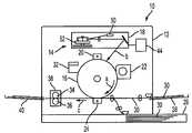
- An image forming section 14may be provided within housing 12 .
- the image forming section 14may include a photoreceptor 16 and an optical scanning device 18 .
- the optical scanning devicemay be a laser Raster Output Scanner (ROS).
- the photoreceptor 16may rotate in a direction of arrow a as shown in FIG. 1 .
- the optical scanning device 18may direct light beams (laser) based on received image data corresponding to pixels in an image to be reproduced toward the photoreceptor 16 (in the direction of arrow b) while scanning.
- a charging unit 20may be disposed in a peripheral surface vicinity of the photoreceptor 16 .
- the charging unit 20charges the photoreceptor 16 as a result of the photoreceptor 16 rotating in the direction of arrow a.
- Polygon mirror 52rotates causing beams b to scan along a path that is parallel to an axis of photoreceptor 16 .
- the intensities of the beamsare modulated in an image wise fashion as they are scanned, selectively discharging the photoreceptor 16 , thereby creating a latent image on the photoreceptor 16 .
- Controller 44may, among other functions, control the on/off timing and power levels of the various laser emitters to produce a desired output based on the image data.
- a transfer charger 24is disposed facing the peripheral surface of the photoreceptor 16 from a position at which the developing unit 22 is disposed (at a position vertically below an axial center of photoreceptor 16 ).
- the transfer charger 24transfers the toner image formed on the peripheral surface of the photoreceptor 16 to paper 30 , which is guided between the photoreceptor 16 and the transfer charger 24 from a paper tray 26 or a manual feed tray 28 .
- a cleaner 32may be disposed facing the photoreceptor 16 , at a downstream side in the rotation direction of the photoreceptor 16 from the position at which the transfer charger 24 is disposed. Toner remaining at the peripheral surface of the photoreceptor 16 after transfer is removed by the cleaner 32 .
- a fixing unit 38which is structured to include a pressure roller 34 and a heating roller 36 , is disposed at a downstream side from the photoreceptor 16 in the direction of ejection of the paper 30 .
- the paper 30 to which the toner image has been transferred and which is being ejectedis subjected to pressure and heated, and the toner is fixed by melting. That is, a “fixing process” is performed at the fixing unit 38 , and the predetermined image is recorded on the paper 30 .
- the fixing processis achieved, and the paper on which the image has been recorded is ejected to a discharge tray 40 or the like.
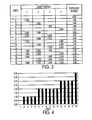
- FIG. 3illustrates a table in which each of the laser beams has a power level of 0 or 1.
- the 16 possible combinations of possible on/off states for the four laser beams of each scan line, and their total power level,are illustrated. This data is further shown in chart form in FIG. 4 . If each of the four laser beams of each row has a power output of 1 or 0, there are five unique exposure levels: 0, 1, 2, 3 and 4, and several combinations yield the same total power level. Accordingly, for any desired total power level, different combinations of on/off among the lasers may be selected by the controller so as to not overuse any of the lasers. For example, to get a desired power level of 2, any two of the four lasers may be on and any two may be off.
- FIG. 5illustrates a table in which each of the laser emitters emits a beam having a power level which has been determined to achieve sixteen different total power levels that vary linearly, and are substantially linearly spaced, with the maximum total power level for all four laser beams being normalized to one unit.
- FIG. 6shows the same data in chart form.
- FIG. 7illustrates an exposure envelope for four laser beams scanning a particular spot on a scanning line.
- Embodimentsmay utilize the controller to control and vary the on timing and off timing of the laser beams as they scan a spot along a scan line to produce a scan envelope varying with time as desired across the particular spot. This allows variation in the exposure level (and hence the gray level) within each pixel.
- This exposure envelopemay be applied at a pixel (or spot) level, at a sub-pixel level, or across multiple pixels.
- the VCSEL arrayhas been described as an emitter that may be used. However, alternative emitters may also be used, such as a dual beam monolithic emitter, which may be used to scan single lines with two laser beams having four unique power levels. Also, a quad beam emitter could be used to scan a single scan line at a time with four laser beams and produce 16 unique levels with overwrite.
- each of the laser emittersis individually controlled to selectively apply one of a plurality of power levels from each of the laser beams based on the image data for each of the pixels, wherein a total power applied by the laser beams for each pixel is determined by a sum of the power levels applied by each of the laser beams.
- the methodstops.
- Computer-executable instructionsinclude, for example, instructions and data which cause a general purpose computer, special purpose computer, or special purpose processing device to perform a certain function or group of functions.
- Computer-executable instructionsalso include program modules that are executed by computers in stand-alone or network environments.
- program modulesinclude routines, programs, objects, components, and data structures, and the like that perform particular tasks or implement particular abstract data types.
- Computer-executable instructions, associated data structures, and program modulesrepresent examples of the program code means for executing steps of the methods disclosed herein.
- the particular sequence of such executable instructions or associated data structuresrepresents examples of corresponding acts for implementing the functions described therein.
- the instructions for carrying out the functionality of the disclosed embodimentsmay be stored on such a computer-readable medium.
Landscapes
- Physics & Mathematics (AREA)
- Optics & Photonics (AREA)
- Health & Medical Sciences (AREA)
- General Health & Medical Sciences (AREA)
- Toxicology (AREA)
- Facsimile Scanning Arrangements (AREA)
- Laser Beam Printer (AREA)
- Mechanical Optical Scanning Systems (AREA)
Abstract
Description
Claims (11)
Priority Applications (1)
| Application Number | Priority Date | Filing Date | Title |
|---|---|---|---|
| US12/060,513US8217975B2 (en) | 2008-04-01 | 2008-04-01 | Apparatus for forming an image and corresponding methods |
Applications Claiming Priority (1)
| Application Number | Priority Date | Filing Date | Title |
|---|---|---|---|
| US12/060,513US8217975B2 (en) | 2008-04-01 | 2008-04-01 | Apparatus for forming an image and corresponding methods |
Publications (2)
| Publication Number | Publication Date |
|---|---|
| US20090244252A1 US20090244252A1 (en) | 2009-10-01 |
| US8217975B2true US8217975B2 (en) | 2012-07-10 |
Family
ID=41116524
Family Applications (1)
| Application Number | Title | Priority Date | Filing Date |
|---|---|---|---|
| US12/060,513Expired - Fee RelatedUS8217975B2 (en) | 2008-04-01 | 2008-04-01 | Apparatus for forming an image and corresponding methods |
Country Status (1)
| Country | Link |
|---|---|
| US (1) | US8217975B2 (en) |
Families Citing this family (4)
| Publication number | Priority date | Publication date | Assignee | Title |
|---|---|---|---|---|
| JP2009023176A (en)* | 2007-07-18 | 2009-02-05 | Canon Inc | Scanning optical apparatus and image forming apparatus |
| JP5707830B2 (en)* | 2009-10-19 | 2015-04-30 | 株式会社リコー | Image processing method and image processing apparatus |
| US8334887B2 (en)* | 2010-03-25 | 2012-12-18 | Xerox Corporation | Apparatus and method for determining beam delays in a printing device |
| WO2023075777A1 (en)* | 2021-10-28 | 2023-05-04 | Hewlett-Packard Development Company, L.P. | Power levels in halftoned image data |
Citations (14)
| Publication number | Priority date | Publication date | Assignee | Title |
|---|---|---|---|---|
| US5319393A (en) | 1992-04-02 | 1994-06-07 | Xerox Corporation | Multiple-spot beam control for a raster output scanner an electrophotographic printer |
| US5471236A (en)* | 1991-02-28 | 1995-11-28 | Fuji Xerox Co., Ltd. | Multi-beam scan optical system |
| US5550668A (en)* | 1994-11-21 | 1996-08-27 | Xerox Corporation | Multispot polygon ROS with maximized line separation depth of focus |
| US5589870A (en)* | 1994-10-31 | 1996-12-31 | Xerox Corporation | Spot profile control using fractional interlace factors in a polygon ROS |
| US5638107A (en)* | 1993-10-28 | 1997-06-10 | Xerox Corporation | Interlace formatting in a hyperacuity printer |
| US5995267A (en)* | 1998-01-30 | 1999-11-30 | Xerox Corporation | Time division multiplexing multiple beam raster output scanning system |
| US6038051A (en)* | 1996-12-16 | 2000-03-14 | Fuji Xerox Co., Ltd. | Light scanning device, optical device, and scanning method of optical device |
| US6049408A (en)* | 1998-01-14 | 2000-04-11 | Fuji Xerox Co., Ltd. | Optical scanning apparatus |
| US6057953A (en)* | 1998-12-21 | 2000-05-02 | Xerox Corporation | Dual beam double pass raster output scanner |
| US6078341A (en)* | 1998-12-14 | 2000-06-20 | Xerox Corporation | Laser diode raster output scanners with interlaced scan lines |
| US6104523A (en)* | 1998-12-21 | 2000-08-15 | Xerox Corporation | Dual beam double pass raster output scanner |
| US6137522A (en)* | 1998-01-07 | 2000-10-24 | Xerox Corporation | Raster output scanner exposure control for bias and run levels in a multiple diode system |
| US6160610A (en)* | 1997-11-18 | 2000-12-12 | Fuji Xerox Co., Ltd. | Image forming device and method for controlling divisional light scanning device |
| US20060092264A1 (en)* | 2004-10-29 | 2006-05-04 | Fuji Xerox Co., Ltd. | Image forming apparatus and image forming method |
Family Cites Families (14)
| Publication number | Priority date | Publication date | Assignee | Title |
|---|---|---|---|---|
| US5146240A (en)* | 1990-02-08 | 1992-09-08 | Ricoh Company, Ltd. | Image forming apparatus with plural dot densities |
| US5323179A (en)* | 1991-08-23 | 1994-06-21 | Eastman Kodak Company | Method of calibrating a multichannel printer |
| US5220348A (en)* | 1991-08-23 | 1993-06-15 | Eastman Kodak Company | Electronic drive circuit for multi-laser thermal printer |
| US5510824A (en)* | 1993-07-26 | 1996-04-23 | Texas Instruments, Inc. | Spatial light modulator array |
| US5900901A (en)* | 1995-06-05 | 1999-05-04 | Xerox Corporation | Method and apparatus for compensating for raster position errors in output scanners |
| JP3679621B2 (en)* | 1998-09-14 | 2005-08-03 | 株式会社リコー | Image forming apparatus |
| US6229555B1 (en)* | 2000-05-17 | 2001-05-08 | Lexmark International, Inc. | Method and apparatus for minimizing visual artifacts generated by an electrophotographic machine during imaging |
| JP2004101656A (en)* | 2002-09-05 | 2004-04-02 | Ricoh Co Ltd | Image forming apparatus, optical writing apparatus, and APC control method for optical writing apparatus |
| CN1824499A (en)* | 2005-02-24 | 2006-08-30 | 海德堡印刷机械股份公司 | Method of producing a printing form |
| US7394479B2 (en)* | 2005-03-02 | 2008-07-01 | Marken Corporation | Pulsed laser printing |
| EP2200036A1 (en)* | 2005-04-29 | 2010-06-23 | Hitachi-LG Data Storage Korea Inc. | Method and apparatus for setting laser power in optical disc drive |
| US7576765B2 (en)* | 2005-05-11 | 2009-08-18 | Hewlett-Packard Development Company, L.P. | Methods and apparatus for detecting and optimizing laser mark quality on recording media |
| US7538788B2 (en)* | 2006-05-01 | 2009-05-26 | Hewlett-Packard Development Company, L.P. | Label writing |
| US20080018727A1 (en)* | 2006-07-24 | 2008-01-24 | Kabushiki Kaisha Toshiba | Optical beam scanning apparatus, optical beam scanning method, optical beam scanning program, image forming apparatus, image forming method, image forming program |
- 2008
- 2008-04-01USUS12/060,513patent/US8217975B2/ennot_activeExpired - Fee Related
Patent Citations (15)
| Publication number | Priority date | Publication date | Assignee | Title |
|---|---|---|---|---|
| US5471236A (en)* | 1991-02-28 | 1995-11-28 | Fuji Xerox Co., Ltd. | Multi-beam scan optical system |
| US5319393A (en) | 1992-04-02 | 1994-06-07 | Xerox Corporation | Multiple-spot beam control for a raster output scanner an electrophotographic printer |
| US5638107A (en)* | 1993-10-28 | 1997-06-10 | Xerox Corporation | Interlace formatting in a hyperacuity printer |
| US5589870A (en)* | 1994-10-31 | 1996-12-31 | Xerox Corporation | Spot profile control using fractional interlace factors in a polygon ROS |
| US5550668A (en)* | 1994-11-21 | 1996-08-27 | Xerox Corporation | Multispot polygon ROS with maximized line separation depth of focus |
| US6038051A (en)* | 1996-12-16 | 2000-03-14 | Fuji Xerox Co., Ltd. | Light scanning device, optical device, and scanning method of optical device |
| US6160610A (en)* | 1997-11-18 | 2000-12-12 | Fuji Xerox Co., Ltd. | Image forming device and method for controlling divisional light scanning device |
| US6137522A (en)* | 1998-01-07 | 2000-10-24 | Xerox Corporation | Raster output scanner exposure control for bias and run levels in a multiple diode system |
| US6049408A (en)* | 1998-01-14 | 2000-04-11 | Fuji Xerox Co., Ltd. | Optical scanning apparatus |
| US6115165A (en)* | 1998-01-14 | 2000-09-05 | Fuji Xerox Co., Ltd. | Optical scanning apparatus |
| US5995267A (en)* | 1998-01-30 | 1999-11-30 | Xerox Corporation | Time division multiplexing multiple beam raster output scanning system |
| US6078341A (en)* | 1998-12-14 | 2000-06-20 | Xerox Corporation | Laser diode raster output scanners with interlaced scan lines |
| US6057953A (en)* | 1998-12-21 | 2000-05-02 | Xerox Corporation | Dual beam double pass raster output scanner |
| US6104523A (en)* | 1998-12-21 | 2000-08-15 | Xerox Corporation | Dual beam double pass raster output scanner |
| US20060092264A1 (en)* | 2004-10-29 | 2006-05-04 | Fuji Xerox Co., Ltd. | Image forming apparatus and image forming method |
Also Published As
| Publication number | Publication date |
|---|---|
| US20090244252A1 (en) | 2009-10-01 |
Similar Documents
| Publication | Publication Date | Title |
|---|---|---|
| US8957928B2 (en) | Image forming apparatus | |
| US10133971B2 (en) | Image forming apparatus and method for driving light source | |
| US5808656A (en) | Arrangement and process for generating a matrix image on a photosensitive recording substrate | |
| US20090067882A1 (en) | Image forming apparatus, beam scanning apparatus thereof, and method of beam scanning thereof | |
| US8217975B2 (en) | Apparatus for forming an image and corresponding methods | |
| US8199376B2 (en) | Image forming apparatus and image forming method | |
| JP4474143B2 (en) | Method for adjusting image plane position on scanned surface of optical scanning device | |
| US8605131B2 (en) | Image forming apparatus and image forming method | |
| JP2003182139A (en) | Imaging apparatus | |
| US20220026707A1 (en) | Optical scanning device and image forming apparatus | |
| JP2000000999A (en) | Laser printer and control method therefor | |
| US9007414B2 (en) | Image forming apparatus and test image forming method | |
| US8259147B2 (en) | Image forming apparatus and method of controlling the same | |
| US8125504B2 (en) | Image forming apparatus and control program of image forming apparatus | |
| JPH10253904A (en) | Light source device and light beam optical scanner | |
| JP3832087B2 (en) | Optical beam scanning optical device | |
| JP2002113903A (en) | Latent image forming device, imaging device, controlling method for imaging device and process cartridge | |
| JP2007109929A (en) | Two-dimensional VCSEL array driving apparatus, driving method, image forming method, optical scanning apparatus, and image forming apparatus | |
| JP2007199556A (en) | Optical scanning device, method for controlling the device, and image forming apparatus using the device | |
| JP2013222037A (en) | Image forming apparatus and method for forming test image | |
| JP2015161775A (en) | Image forming apparatus | |
| US8115795B2 (en) | Two-dimensional ROS emitter geometry with low banding sensitivity | |
| JP5441742B2 (en) | Image forming apparatus and light amount correction method thereof | |
| JP2008036992A (en) | Image writing apparatus and image forming apparatus | |
| JPH08318640A (en) | Lensless printing machine equipped with optical bar print head |
Legal Events
| Date | Code | Title | Description |
|---|---|---|---|
| AS | Assignment | Owner name:XEROX CORPORATION, CONNECTICUT Free format text:ASSIGNMENT OF ASSIGNORS INTEREST;ASSIGNORS:KLECKNER, ROBERT J.;PEPE, MARTIN;REEL/FRAME:020736/0651;SIGNING DATES FROM 20080328 TO 20080401 Owner name:PALO ALTO RESEARCH CENTER INCORPORATED, CALIFORNIA Free format text:ASSIGNMENT OF ASSIGNORS INTEREST;ASSIGNOR:MAEDA, PATRICK YASUO;REEL/FRAME:020736/0763 Effective date:20080327 Owner name:XEROX CORPORATION, CONNECTICUT Free format text:ASSIGNMENT OF ASSIGNORS INTEREST;ASSIGNORS:KLECKNER, ROBERT J.;PEPE, MARTIN;SIGNING DATES FROM 20080328 TO 20080401;REEL/FRAME:020736/0651 | |
| FEPP | Fee payment procedure | Free format text:PAYOR NUMBER ASSIGNED (ORIGINAL EVENT CODE: ASPN); ENTITY STATUS OF PATENT OWNER: LARGE ENTITY | |
| ZAAA | Notice of allowance and fees due | Free format text:ORIGINAL CODE: NOA | |
| ZAAB | Notice of allowance mailed | Free format text:ORIGINAL CODE: MN/=. | |
| ZAAA | Notice of allowance and fees due | Free format text:ORIGINAL CODE: NOA | |
| STCF | Information on status: patent grant | Free format text:PATENTED CASE | |
| FPAY | Fee payment | Year of fee payment:4 | |
| MAFP | Maintenance fee payment | Free format text:PAYMENT OF MAINTENANCE FEE, 8TH YEAR, LARGE ENTITY (ORIGINAL EVENT CODE: M1552); ENTITY STATUS OF PATENT OWNER: LARGE ENTITY Year of fee payment:8 | |
| AS | Assignment | Owner name:XEROX CORPORATION, CONNECTICUT Free format text:ASSIGNMENT OF ASSIGNORS INTEREST;ASSIGNOR:PALO ALTO RESEARCH CENTER INCORPORATED;REEL/FRAME:064038/0001 Effective date:20230416 | |
| AS | Assignment | Owner name:CITIBANK, N.A., AS COLLATERAL AGENT, NEW YORK Free format text:SECURITY INTEREST;ASSIGNOR:XEROX CORPORATION;REEL/FRAME:064760/0389 Effective date:20230621 | |
| AS | Assignment | Owner name:XEROX CORPORATION, CONNECTICUT Free format text:CORRECTIVE ASSIGNMENT TO CORRECT THE REMOVAL OF US PATENTS 9356603, 10026651, 10626048 AND INCLUSION OF US PATENT 7167871 PREVIOUSLY RECORDED ON REEL 064038 FRAME 0001. ASSIGNOR(S) HEREBY CONFIRMS THE ASSIGNMENT;ASSIGNOR:PALO ALTO RESEARCH CENTER INCORPORATED;REEL/FRAME:064161/0001 Effective date:20230416 | |
| AS | Assignment | Owner name:JEFFERIES FINANCE LLC, AS COLLATERAL AGENT, NEW YORK Free format text:SECURITY INTEREST;ASSIGNOR:XEROX CORPORATION;REEL/FRAME:065628/0019 Effective date:20231117 | |
| AS | Assignment | Owner name:XEROX CORPORATION, CONNECTICUT Free format text:TERMINATION AND RELEASE OF SECURITY INTEREST IN PATENTS RECORDED AT RF 064760/0389;ASSIGNOR:CITIBANK, N.A., AS COLLATERAL AGENT;REEL/FRAME:068261/0001 Effective date:20240206 Owner name:CITIBANK, N.A., AS COLLATERAL AGENT, NEW YORK Free format text:SECURITY INTEREST;ASSIGNOR:XEROX CORPORATION;REEL/FRAME:066741/0001 Effective date:20240206 | |
| FEPP | Fee payment procedure | Free format text:MAINTENANCE FEE REMINDER MAILED (ORIGINAL EVENT CODE: REM.); ENTITY STATUS OF PATENT OWNER: LARGE ENTITY | |
| LAPS | Lapse for failure to pay maintenance fees | Free format text:PATENT EXPIRED FOR FAILURE TO PAY MAINTENANCE FEES (ORIGINAL EVENT CODE: EXP.); ENTITY STATUS OF PATENT OWNER: LARGE ENTITY | |
| STCH | Information on status: patent discontinuation | Free format text:PATENT EXPIRED DUE TO NONPAYMENT OF MAINTENANCE FEES UNDER 37 CFR 1.362 | |
| FP | Lapsed due to failure to pay maintenance fee | Effective date:20240710 |