US8217916B2 - Display device with touch panel - Google Patents
Display device with touch panelDownload PDFInfo
- Publication number
- US8217916B2 US8217916B2US12/493,391US49339109AUS8217916B2US 8217916 B2US8217916 B2US 8217916B2US 49339109 AUS49339109 AUS 49339109AUS 8217916 B2US8217916 B2US 8217916B2
- Authority
- US
- United States
- Prior art keywords
- electrodes
- touch panel
- display device
- electrode
- transparent conductive
- Prior art date
- Legal status (The legal status is an assumption and is not a legal conclusion. Google has not performed a legal analysis and makes no representation as to the accuracy of the status listed.)
- Active, expires
Links
Images


Classifications
- G—PHYSICS
- G06—COMPUTING OR CALCULATING; COUNTING
- G06F—ELECTRIC DIGITAL DATA PROCESSING
- G06F3/00—Input arrangements for transferring data to be processed into a form capable of being handled by the computer; Output arrangements for transferring data from processing unit to output unit, e.g. interface arrangements
- G06F3/01—Input arrangements or combined input and output arrangements for interaction between user and computer
- G06F3/03—Arrangements for converting the position or the displacement of a member into a coded form
- G06F3/041—Digitisers, e.g. for touch screens or touch pads, characterised by the transducing means
- G06F3/0416—Control or interface arrangements specially adapted for digitisers
- G06F3/04164—Connections between sensors and controllers, e.g. routing lines between electrodes and connection pads
- G—PHYSICS
- G06—COMPUTING OR CALCULATING; COUNTING
- G06F—ELECTRIC DIGITAL DATA PROCESSING
- G06F3/00—Input arrangements for transferring data to be processed into a form capable of being handled by the computer; Output arrangements for transferring data from processing unit to output unit, e.g. interface arrangements
- G06F3/01—Input arrangements or combined input and output arrangements for interaction between user and computer
- G06F3/03—Arrangements for converting the position or the displacement of a member into a coded form
- G06F3/041—Digitisers, e.g. for touch screens or touch pads, characterised by the transducing means
- G06F3/0412—Digitisers structurally integrated in a display
- G—PHYSICS
- G06—COMPUTING OR CALCULATING; COUNTING
- G06F—ELECTRIC DIGITAL DATA PROCESSING
- G06F3/00—Input arrangements for transferring data to be processed into a form capable of being handled by the computer; Output arrangements for transferring data from processing unit to output unit, e.g. interface arrangements
- G06F3/01—Input arrangements or combined input and output arrangements for interaction between user and computer
- G06F3/03—Arrangements for converting the position or the displacement of a member into a coded form
- G06F3/041—Digitisers, e.g. for touch screens or touch pads, characterised by the transducing means
- G06F3/044—Digitisers, e.g. for touch screens or touch pads, characterised by the transducing means by capacitive means
- G06F3/0443—Digitisers, e.g. for touch screens or touch pads, characterised by the transducing means by capacitive means using a single layer of sensing electrodes
- G—PHYSICS
- G06—COMPUTING OR CALCULATING; COUNTING
- G06F—ELECTRIC DIGITAL DATA PROCESSING
- G06F3/00—Input arrangements for transferring data to be processed into a form capable of being handled by the computer; Output arrangements for transferring data from processing unit to output unit, e.g. interface arrangements
- G06F3/01—Input arrangements or combined input and output arrangements for interaction between user and computer
- G06F3/03—Arrangements for converting the position or the displacement of a member into a coded form
- G06F3/041—Digitisers, e.g. for touch screens or touch pads, characterised by the transducing means
- G06F3/044—Digitisers, e.g. for touch screens or touch pads, characterised by the transducing means by capacitive means
- G06F3/0446—Digitisers, e.g. for touch screens or touch pads, characterised by the transducing means by capacitive means using a grid-like structure of electrodes in at least two directions, e.g. using row and column electrodes
- G—PHYSICS
- G06—COMPUTING OR CALCULATING; COUNTING
- G06F—ELECTRIC DIGITAL DATA PROCESSING
- G06F3/00—Input arrangements for transferring data to be processed into a form capable of being handled by the computer; Output arrangements for transferring data from processing unit to output unit, e.g. interface arrangements
- G06F3/01—Input arrangements or combined input and output arrangements for interaction between user and computer
- G06F3/03—Arrangements for converting the position or the displacement of a member into a coded form
- G06F3/041—Digitisers, e.g. for touch screens or touch pads, characterised by the transducing means
- G06F3/045—Digitisers, e.g. for touch screens or touch pads, characterised by the transducing means using resistive elements, e.g. a single continuous surface or two parallel surfaces put in contact
- G—PHYSICS
- G09—EDUCATION; CRYPTOGRAPHY; DISPLAY; ADVERTISING; SEALS
- G09G—ARRANGEMENTS OR CIRCUITS FOR CONTROL OF INDICATING DEVICES USING STATIC MEANS TO PRESENT VARIABLE INFORMATION
- G09G3/00—Control arrangements or circuits, of interest only in connection with visual indicators other than cathode-ray tubes
- G09G3/20—Control arrangements or circuits, of interest only in connection with visual indicators other than cathode-ray tubes for presentation of an assembly of a number of characters, e.g. a page, by composing the assembly by combination of individual elements arranged in a matrix no fixed position being assigned to or needed to be assigned to the individual characters or partial characters
- G09G3/34—Control arrangements or circuits, of interest only in connection with visual indicators other than cathode-ray tubes for presentation of an assembly of a number of characters, e.g. a page, by composing the assembly by combination of individual elements arranged in a matrix no fixed position being assigned to or needed to be assigned to the individual characters or partial characters by control of light from an independent source
- G09G3/36—Control arrangements or circuits, of interest only in connection with visual indicators other than cathode-ray tubes for presentation of an assembly of a number of characters, e.g. a page, by composing the assembly by combination of individual elements arranged in a matrix no fixed position being assigned to or needed to be assigned to the individual characters or partial characters by control of light from an independent source using liquid crystals
- G—PHYSICS
- G06—COMPUTING OR CALCULATING; COUNTING
- G06F—ELECTRIC DIGITAL DATA PROCESSING
- G06F2203/00—Indexing scheme relating to G06F3/00 - G06F3/048
- G06F2203/041—Indexing scheme relating to G06F3/041 - G06F3/045
- G06F2203/04103—Manufacturing, i.e. details related to manufacturing processes specially suited for touch sensitive devices
- G—PHYSICS
- G06—COMPUTING OR CALCULATING; COUNTING
- G06F—ELECTRIC DIGITAL DATA PROCESSING
- G06F2203/00—Indexing scheme relating to G06F3/00 - G06F3/048
- G06F2203/041—Indexing scheme relating to G06F3/041 - G06F3/045
- G06F2203/04111—Cross over in capacitive digitiser, i.e. details of structures for connecting electrodes of the sensing pattern where the connections cross each other, e.g. bridge structures comprising an insulating layer, or vias through substrate
- G—PHYSICS
- G06—COMPUTING OR CALCULATING; COUNTING
- G06F—ELECTRIC DIGITAL DATA PROCESSING
- G06F2203/00—Indexing scheme relating to G06F3/00 - G06F3/048
- G06F2203/041—Indexing scheme relating to G06F3/041 - G06F3/045
- G06F2203/04112—Electrode mesh in capacitive digitiser: electrode for touch sensing is formed of a mesh of very fine, normally metallic, interconnected lines that are almost invisible to see. This provides a quite large but transparent electrode surface, without need for ITO or similar transparent conductive material
Definitions
- the present inventionrelates to a display device with a touch panel, and more particularly, to a technology effectively applicable to a display device with a touch panel that is a capacitive touch panel.
- JP 2003-511799 Adiscloses a touch panel that detects a touch point touched by an observer's finger.
- the touch panel described in JP 2003-511799 Adetects the coordinates of a point touched by an observer through detection of a coupling capacitance between an electrode in an X direction and an electrode in a Y direction.
- a common capacitive touch panelincludes a plurality of X electrodes which extend in a first direction (for example, Y direction) and are placed next to one another in a second direction (for example, X direction) intersecting the first direction, and a plurality of Y electrodes which extend in the second direction to intersect the X electrodes and are placed next to one another in the first direction. Touch panels of this type are called X-Y touch panels.
- the plurality of X electrodes and the plurality of Y electrodes in an X-Y touch panelare formed on a substrate with an interlayer insulating film interposed between the X electrode layer and the Y electrode layer.
- Those X electrodes and Y electrodesare formed of a transparent conductive material such as indium tin oxide (ITO).
- the capacitance of one line of electrodes in a steady state where the touch panel is not being touched by a finger or the likeincludes an inter-electrode capacitance with an adjacent electrode, an intersection capacitance formed at the intersection of orthogonal electrodes, and a ground capacitance with a display device placed under the touch panel.
- An index of their detection sensitivitywhich is the ratio of a change in capacitance that is caused by a touch of a finger or the like to background noise (hereinafter referred to as S/N ratio), is used. Raising the detection sensitivity, i.e., the S/N ratio, requires increasing signals or reducing noise.
- the signal levelis in proportion to the capacitance that is formed between a finger or the like touching the touch panel and an electrode.
- a fact found about background noiseis that the fluctuations in voltage of a signal generated by the display device in order to display an image are detected as noise by electrodes of the touch panel which is located right above the display device. It is easier to detect the noise when the total electrode area along one line of electrodes is larger because the ground capacitance is accordingly larger.
- the touch panel overlaid on the display device when in usehas substantially the same contour as that of the display device.
- the display devicegenerally has a rectangular shape which is longer in the X direction or in the Y direction.
- individual electrodes constituting one line in the X direction and individual electrodes constituting one line in the Y directionare equal in size whereas one line of electrodes in the X direction and one line of electrodes in the Y direction differ from each other in length and in the number of individual electrodes constituting one line.
- the capacitance of one line of electrodes in the X directiontherefore differs from the capacitance of one line of electrodes in the Y direction.
- the capacitance of one line of X electrodes which are arranged parallel to one another in the Y directionis larger than the capacitance of one line of Y electrodes which are arranged parallel to one another in the X direction.
- the difference in capacitance along one line of electrodes between the X direction and the Y directionmeans that the noise intensity differs between the X direction and the Y direction in touch panels of the related art.
- the S/N ratiodiffers between the X direction and the Y direction in touch panels of the related art.
- the overall detection sensitivity of the touch panelis defined by the lower one of the differing S/N ratios.
- the present inventionhas been made in view of described above, and an object of the present invention is therefore to provide a display device with a touch panel that has a large S/N ratio and a high detection sensitivity.
- the noise intensity ratio of the X electrodes to the Y electrodesis substantially equal to the X electrode-to-Y electrode capacitance ratio, namely, X electrode-to-Y electrode count ratio.
- the present inventionis based on the above-mentioned findings.
- the above-mentioned objectis attained by: reducing the area of each individual electrode on a line of electrodes that runs along the longer sides of an input region of a touch panel; setting the ratio of the area of each individual electrode on this line of electrodes to the area of each individual electrode on another line of electrodes, which is orthogonal to the former line of electrodes, to a value smaller than the ratio of the electrode count of the line of electrodes that runs along the input region's longer side direction to the electrode count of the line of electrodes that runs along the input region's shorter side direction by 10% or less so that the capacitance along one line of electrodes is substantially equal to the capacitance along the other line of electrodes; and disposing floating electrodes (dummy electrodes) in places freed up by the area reduction.
- a display device with a touch panelwhich includes: a display panel; and a capacitive touch panel formed to be overlaid on the display panel, and is characterized in that: the touch panel includes X electrodes and Y electrodes which intersect the X electrodes; the X electrodes and the Y electrodes include intersection portions at which the X electrodes and the Y electrodes overlap each other, and electrode portions each formed between two of the intersection portions; and one of the electrode portions of the X electrode and the electrode portions of the Y electrode is smaller in area than another thereof so that a capacitance of one line of the X electrodes and a capacitance of one line of the Y electrodes are equal to each other.
- a display device with a touch panelwhich includes: a display panel; and a capacitive touch panel bonded onto the display panel, and is characterized in that:: the touch panel includes X electrodes and Y electrodes which intersect the X electrodes; the display panel has longer sides and shorter sides; the X electrodes and the Y electrodes include intersection portions at which the X electrodes and the Y electrodes overlap each other, and individual electrodes each formed between two of the intersection portions and being wider than the intersection portions; the X electrodes are formed along the longer sides whereas the Y electrodes are formed along the shorter sides; and each individual electrode of the X electrodes is smaller in area than each individual electrode of the Y electrodes.
- a display device with a touch panelwhich includes: a display panel; and a capacitive touch panel placed on the display panel, and is characterized in that: the touch panel includes X electrodes and Y electrodes which intersect the X electrodes; the X electrodes and the Y electrodes include intersection portions at which the X electrodes and the Y electrodes overlap each other, and individual electrodes each formed between two of the intersection portions and being wider than the intersection portions; the a number of the individual electrodes of the X electrodes is n and a number of the individual electrodes of the Y electrodes is m; and a ratio between an area of the individual electrodes of the X electrodes and an area of the individual electrodes of the Y electrodes is m:n.
- a display device with a touch panelthat has a large S/N ratio and a high detection sensitivity.
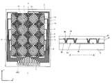
- FIG. 1is a plan view illustrating a schematic structure of a display device with a touch panel according to an embodiment of the present invention
- FIG. 2is a sectional view illustrating a sectional structure taken along the line A-A′ of FIG. 1 ;
- FIG. 3is a plan view illustrating an electrode pattern of a capacitive touch panel according to the embodiment of the present invention.
- FIG. 4is a graph illustrating a change in S/N ratio of a capacitive touch panel when an area of each individual electrode of X electrodes, which is arranged parallel to each other in a longitudinal direction, is varied;
- FIG. 5is a sectional view illustrating a sectional structure of the line B-B′ at the first step of the method of manufacturing the touch panel according to the embodiment of the present invention
- FIG. 6is a sectional view illustrating the sectional structure of the line B-B′ at the second step of the method of manufacturing the touch panel according to the embodiment of the present invention
- FIG. 7is a sectional view illustrating the sectional structure of the line B-B′ at the third step of the method of manufacturing the touch panel according to the embodiment of the present invention.
- FIG. 8is a sectional view illustrating the sectional structure of the line B-B′ at the fourth step of the method of manufacturing the touch panel according to the embodiment of the present invention.
- FIG. 9is a sectional view illustrating a sectional structure of the line C-C′ at the first step of the method of manufacturing the touch panel according to the embodiment of the present invention.
- FIG. 10is a sectional view illustrating the sectional structure of the line C-C′ at the second step of the method of manufacturing the touch panel according to the embodiment of the present invention.
- FIG. 11is a sectional view illustrating the sectional structure of the line C-C′ at the third step of the method of manufacturing the touch panel according to the embodiment of the present invention.
- FIG. 12is a sectional view illustrating the sectional structure of the line C-C′ at the fourth step of the method of manufacturing the touch panel according to the embodiment of the present invention.
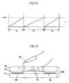
- FIG. 13is a diagram illustrating a state in which an observer's finger is touching the touch panel according to the embodiment of the present invention.
- FIG. 14is a diagram illustrating an operation of detecting an input point of the touch panel according to the embodiment of the present invention.
- FIG. 15is a plan view illustrating an electrode pattern of another touch panel to which the present invention is applied.
- FIG. 16is a sectional view illustrating a sectional structure taken along the line A-A′ of FIG. 15 .
- liquid crystal display panelas an example of a display panel. Any display panel can be employed as long as it allows the use of a touch panel and, other than liquid crystal display panels, display panels that use organic light emitting diode elements or surface conduction electron emitter elements are employable.
- FIG. 1is a plan view illustrating a schematic structure of a display device with a touch panel according to the embodiment of the present invention.
- FIG. 2is a sectional view taken along the line A-A′ of FIG. 1 .
- a display device with a touch panel 300 of this embodimentincludes, as illustrated in FIGS. 1 and 2 , a liquid crystal display panel 600 , a capacitive touch panel 400 which is placed on an observer side of the liquid crystal display panel 600 , and a backlight 700 which is placed on the opposite side of the liquid crystal display panel 600 from the observer side.
- the liquid crystal display panel 600can be, for example, an in plane switching (IPS) liquid crystal display panel, a twisted nematic (TN) liquid crystal display panel, or a vertical alignment (VA) liquid crystal display panel.
- IPSin plane switching
- TNtwisted nematic
- VAvertical alignment
- the liquid crystal display panel 600is formed by bonding together two substrates that are opposed to each other.
- Polarizing plates 601 and 602are provided on the exteriors of the two substrates.
- the liquid crystal display panel 600 and the touch panel 400are bonded to each other with a first bonding member 501 which is a resin film, an adhesive film, or the like.
- a second bonding member 502which is a resin film, an adhesive film, or the like bonds a front surface protecting plate (also called front window) 12 made of an acrylic resin to the exterior of the touch panel 400 .
- a transparent conductive layer 603is provided between the liquid crystal display panel 600 and the polarizing plate 601 .
- the transparent conductive layer 603is formed to shield against signals generated by the liquid crystal display panel 600 .
- a large number of electrodesare provided on the liquid crystal display panel 600 and voltages are applied as signals to the electrodes on various timings.
- a change in voltage on the liquid crystal display panel 600is noise to electrodes that are provided on the capacitive touch panel 400 .
- the liquid crystal display panel 600therefore needs to be electrically shielded, and this is why the transparent conductive layer 603 is provided.
- the transparent conductive layer 603receives a supply of a constant voltage from a flexible printed board 71 or others, and is set to, for example, a ground potential.
- the transparent conductive layer 603desirably has a sheet resistance value approximately equal to that of the electrodes provided on the touch panel 400 , specifically, 150 to 200 ⁇ /square, for reducing the influence of the noise.
- the resistance value of the transparent conductive layer 603is known to have a relation with the crystal grain size.
- the transparent conductive layer 603can have a sheet resistance value of 150 to 200 ⁇ /square by setting the heat treatment temperature to 200° C. or higher for crystallizing.
- the transparent conductive layer 603may have an even lower resistance. For example, setting the heat treatment temperature to 450° C. and thereby crystallizing the transparent conductive layer 603 thoroughly gives the transparent conductive layer 603 a sheet resistance value of 10 to 40 ⁇ /square. The effect of reducing the noise is improved when the shielding transparent conductive layer 603 has a resistance approximately equal to, or lower than that of the electrodes provided on the touch panel 400 .
- the reverse-surface side transparent conductive filmmay also have a function as the transparent conductive layer 603 .
- a drive circuit 50is provided across from one of the four sides of the liquid crystal display panel 600 , and supplies various signals to image elements inside the liquid crystal display panel 600 .
- a flexible printed board 72is connected to one of the four sides of the liquid crystal display panel 600 in order to supply signals from the outside. The signals are supplied from the outside to the drive circuit 50 via the flexible printed board 72 .
- Another flexible printed board 71is connected to the touch panel 400 .
- a touch panel control circuit 60is mounted to the flexible printed board 71 to control the detection of an input point and other operations.
- a spacer 30is placed between the touch panel 400 and the drive circuit 50 .
- FIG. 3is a plan view illustrating the electrode structure of the touch panel 400 according to this embodiment.
- FIG. 3illustrates a case of using the touch panel 400 vertically long.
- the liquid crystal display panel 600 overlaid with the touch panel 400similarly has a shape vertically long as mentioned above.
- a glass substrate 5is employed as a transparent substrate.
- Touch panel electrodes ( 1 and 2 ), connection terminals 7 , wiring lines 6 extending from the touch panel electrodes ( 1 and 2 ) to the connection terminals 7are placed on one surface of the glass substrate 5 . At least intersection portions of the two touch panel electrodes ( 1 and 2 ) arranged orthogonally to each other are separated by an insulating film.
- the touch panel electrodes ( 1 and 2 )are formed of a transparent conductive film.
- electrodes that extend in the longitudinal direction (Y direction of FIG. 3 ) and are arranged side by side in the lateral direction (X direction)are called X electrodes 1
- electrodes that extend in the lateral direction (X direction) to intersect the X electrodes 1 and are arranged side by side in the longitudinal direction (Y direction)are called Y electrodes 2 .
- the touch panel 400 of this embodimentdetects a change in capacitance of those X electrodes 1 and Y electrodes 2 to calculate a point where the touch panel 400 has been touched.
- a region inside the dotted line, which is denoted by reference numeral 3 and capable of detection,is called an input region.
- the X electrodes 1 and the Y electrodes 2are narrower in intersection portions 1 a and intersection portions 2 a , respectively, and wider in electrode portions 1 b and electrode portions 2 b , respectively.
- Each electrode portion 1 bis sandwiched between two intersection portions 1 a and each electrode portion 2 b is sandwiched between two intersection portions 2 a .
- the electrode portion 1 b sandwiched between the intersection portions 1 a and the electrode portion 2 b sandwiched between the electrode portions 2 aare also called individual electrodes.
- the individual electrodes 1 b of the X electrodes 1are narrower than the individual electrodes 2 b of the Y electrodes 2 as illustrated in FIG. 3 .
- the area of the X electrodes 1is made smaller in a manner that reflects the ratio of the count of the individual electrodes 1 b of the X electrodes 1 to the count of the individual electrodes 2 b of the Y electrodes 2 , and the X electrodes 1 are divided into the individual electrodes 1 b and electrodes (dummy electrodes) 4 which have a floating potential.
- the electrode area of the X electrodes 1 which would be larger as the vertical length of the panel's shape is longeris reduced such that the capacitance along one line of X electrodes 1 is substantially equal to the capacitance along one line of Y electrodes 2 .
- the X electrodes 1 and the Y electrodes 2are thus made equal in terms of noise that is caused by fluctuations in voltage of a signal generated by the liquid crystal display panel 600 .
- the transparent conductive layer 603 provided on the liquid crystal display panel 600reduces the influence of the noise from the liquid crystal display panel 600 .
- forming the transparent conductive layer 603 on the liquid crystal display panel 600 at high temperatureis difficult and, in some cases, it is not possible to form the transparent conductive layer 603 that has sufficiently low resistance on the liquid crystal display panel 600 . Further, even with the transparent conductive layer 603 , the noise from the liquid crystal display panel 600 can still influence.
- FIG. 4is a graph illustrating results of an S/N ratio evaluation on the trial touch panel 400 by varying the area of each individual electrode 1 b along an X electrode line parallel to the longitudinal direction.
- the trial touch panel 400has six X electrodes 1 , ten Y electrodes 2 , an X-to-Y electrode count ratio of 60%, and a shape vertically long.
- the axis of abscissaindicates the area ratio of each individual electrode 1 b to each individual electrode 2 b
- the axis of ordinateindicates the S/N ratio.
- the ground capacitancedecreases and the noise level can be reduced.
- the floating electrodes 4 adjacent to the touched X electrode 1are also touched and caused to function by capacitance coupling.
- the degree of the signal level reductionis therefore smaller than the degree of the area reduction.
- the resultant S/N ratiotherefore has peaked at an area ratio that is equal to the electrode count ratio as illustrated in FIG. 4 .
- an interval 8 between one X electrode 1 and its adjacent Y electrode 2is larger than when the floating electrodes 4 are provided.
- the interval 8is a region that includes the insulating film and the glass substrate but does not include the transparent conductive film of which the X electrodes 1 and the Y electrodes 2 are formed as mentioned above.
- a portion that includes the transparent conductive film and a portion that does not include the transparent conductive filmdiffer from each other in terms of transmittance, reflectance, and chromaticity of reflected light, and hence the interval 8 is visible to the naked eye, which lowers the quality of the displayed image.
- the interval 8has been faintly visible when it is 30 ⁇ m wide, hardly visible at 20 ⁇ m, and invisible at 10 ⁇ m. Narrowing the interval 8 increases the capacitance between the X electrode 1 and the Y electrode 2 that are adjacent to each other with the floating electrode 4 interposed therebetween. Narrowing the interval 8 also increases defects in which unsuccessful pattern formation due to a foreign object attached in the process of manufacture results in a short-circuit between the X electrode 1 or the Y electrode 2 and the floating electrode 4 .
- a short-circuit of the floating electrode 4 adjacent to the individual electrode 1 b of one X electrode 1causes inconveniences such as an increase in ground capacitance of the relevant one line of X electrodes, increased noise, and a decrease in detection sensitivity.
- each floating electrode 4is a 1 ⁇ 4 piece of a whole as illustrated in FIG. 3 . Dividing each floating electrode 4 into more pieces lowers the risk of a short-circuit defect, but increases the regions that do not have the transparent conductive film, which may increase the difference in transmittance, reflectance, and chromaticity between adjacent electrodes. This embodiment therefore chooses to divide each floating electrode 4 into four and set the interval between the electrodes narrower than 30 ⁇ m, specifically, to 20 ⁇ m or so.
- This embodimentshows a case of overlaying a touch panel on a liquid crystal display device vertically long, but the effects of the present invention are similarly obtained when the touch panel is overlaid on a liquid crystal display device vertically long, or on other types of image display device. Further, the number of pieces into which each floating electrode is divided is not limited to four.
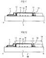
- FIGS. 5 to 13illustrate sectional structures taken along the line B-B′ of FIG. 3 at various process stages.
- FIGS. 9 to 12illustrate sectional structures taken along the line C-C′ of FIG. 3 at various process stages.
- a first stepis described with reference to FIGS. 5 and 9 .
- a first indium tin oxide (ITO) film 14is formed on the glass substrate 5 to have a thickness of about 15 nm, and then a silver alloy film 15 is formed to have a thickness of about 200 nm.
- ITOindium tin oxide
- a resist patternis formed by photolithography process to pattern the silver alloy film 15 .
- the resistis removed and another resist pattern is formed by photolithography process to pattern the first ITO film 14 .
- the resistis removed and the patterned ITO film 14 (Y electrodes 2 ) and silver alloy film 15 (wiring lines 6 ) are formed as illustrated in FIGS. 5 and 9 .
- the silver alloy film 15 which is opaquehas to be prevented from being visible. Then, the silver alloy film 15 is formed as only the peripheral wiring lines 6 by removing a part of the silver alloy film 15 that overlaps with the display region of the liquid crystal display panel 600 , which is overlaid later.
- a second stepis described next with reference to FIGS. 6 and 10 .
- a photosensitive interlayer insulating film 16is formed by application on the substrate on which the first ITO film 14 and the silver alloy film 15 have been patterned.
- the interlayer insulating film 16is patterned through photolithography process.
- the interlayer insulating film 16is desirably a film formed by application of a material that contains SiO 2 as the main component to have a thickness of 1 ⁇ m or more.
- the contact holes 17are formed in the peripheral portion.
- the interlayer insulating film pattern 16is removed from a terminal connection portion which is used for a connection with an external drive circuit.
- a third stepis described next with reference to FIGS. 7 and 11 .
- a second ITO film 18is formed to have a thickness of about 30 nm and a resist pattern is formed by photolithography process to pattern the second ITO film 18 .
- the resistis then removed and the second ITO film 18 (X electrodes 1 ) is formed as illustrated in FIGS. 7 and 11 .
- a fourth stepis described next with reference to FIGS. 8 and 12 .
- the same kind of film as the insulating film used in the second stepis formed on the substrate by application as an uppermost protective film 19 .
- the uppermost protective film 19is patterned by photolithography process.
- the touch panel 400is formed through the above-mentioned steps.
- the touch panel control circuit 60supplies a constant current to the X electrodes 1 and the Y electrodes 2 sequentially to charge the X electrodes 1 or the Y electrodes 2 , and a period T required for the voltage of the X electrodes 1 or the Y electrodes 2 to rise to a given reference voltage (Vref) is measured.
- the period Tis Ta as illustrated in FIG. 13 .
- a capacitor (C)is added to the individual electrodes ( 1 b or 2 b ) of the X electrodes 1 or the Y electrodes 2 , thereby setting the period T to Tb, which is longer than Ta (Ta ⁇ Tb).
- the observer's finger 35is generally larger than the area of the individual electrode ( 1 b or 2 b ) of one X electrode 1 or one Y electrode 2 . Accordingly, the period T that is longer than Ta (for example, the period Tb) is detected in a plurality of X electrodes 1 or a plurality of Y electrodes 2 . Based on the locations of a plurality of electrodes at which the period T that is longer than Ta is detected and the length of the period (for example, Tb) detected in those electrodes, the centroid point is obtained by centroid processing as an input point.
- the above-mentioned period Tis detected from the count of basic clocks (e.g., dot clocks (CLKs) used in the liquid crystal display panel 600 ).
- basic clockse.g., dot clocks (CLKs) used in the liquid crystal display panel 600 .
- the capacitance of one line of the X electrodes and the capacitance of one line of the Y electrodesalso means a capacitance component of impedance viewed from the touch panel control circuit 60 .
- the capacitance of one line of the X electrodes and the capacitance of one line of the Y electrodes are equal to each otheralso means that the above-mentioned period T, or the count of dot clocks (CLKs) within the period T, is equal between the X electrodes and the Y electrodes.
- the capacitance of one line of the X electrodes and the capacitance of one line of the Y electrodes are equal to each othermeans that the capacitance of one line of electrodes is within ⁇ 10% of a designed value.
- the count of dot clocks (CLKs) within the period Tis equal between the X electrodes and the Y electrodes” naturally means that the dot clock count is within ⁇ 10% of a designed value.
- the present inventioncan be applied irrespective of the shape of the input detection region and the shape of the individual electrodes.
- the present inventionis applicable to a touch panel in which the X electrodes 1 and the Y electrodes 2 are formed in the same layer as illustrated in FIGS. 15 and 16 .
- the individual electrodes 1 b of the X electrodes 1 and the individual electrodes 2 b of the Y electrodes 2are formed in the same conductive layer but are separated from each other, whereas the intersection portions 1 a of the X electrodes 1 and the intersection portions 2 a of the Y electrodes 2 are formed in different conductive layers.
- FIG. 16the intersection portions 2 a of the Y electrodes 2 are formed in a layer above the intersection portions 1 a of the X electrodes 1 and intersect the intersection portions 1 a of the X electrodes 1 a .
- the intersection portions 2 a of the Y electrodes 2are connected to the individual electrodes 2 b of the Y electrodes 2 through contact holes 36 formed in the interlayer insulating film 16 .
- FIG. 16is a sectional view illustrating a sectional structure taken along the line A-A′ of FIG. 15 .
- the embodiment abovedescribes X direction electrodes and Y direction electrodes which are orthogonal to each other.
- the present inventionis aimed at averaging the difference in capacitance between electrode lines used in the detection of an input point, and is therefore effective also for an adjustment of the capacitance between electrodes that intersect each other obliquely, or between side-by-side electrode lines that have different lengths.
- a touch panel having an excellent detection sensitivitycan thus be manufactured as a capacitive input device for an image information/text information display device.
Landscapes
- Engineering & Computer Science (AREA)
- Theoretical Computer Science (AREA)
- General Engineering & Computer Science (AREA)
- Physics & Mathematics (AREA)
- General Physics & Mathematics (AREA)
- Human Computer Interaction (AREA)
- Computer Networks & Wireless Communication (AREA)
- Chemical & Material Sciences (AREA)
- Crystallography & Structural Chemistry (AREA)
- Computer Hardware Design (AREA)
- Position Input By Displaying (AREA)
Abstract
Description
Claims (15)
Priority Applications (13)
| Application Number | Priority Date | Filing Date | Title |
|---|---|---|---|
| US13/542,730US8890838B2 (en) | 2008-06-30 | 2012-07-06 | Display device with touch panel |
| US14/533,625US9201555B2 (en) | 2008-06-30 | 2014-11-05 | Display device with touch panel |
| US14/926,972US9513757B2 (en) | 2008-06-30 | 2015-10-29 | Display device with touch panel |
| US15/338,621US9740331B2 (en) | 2008-06-30 | 2016-10-31 | Display device with touch panel |
| US15/653,824US9939954B2 (en) | 2008-06-30 | 2017-07-19 | Touch panel |
| US15/908,897US10133410B2 (en) | 2008-06-30 | 2018-03-01 | Touch panel having X electrodes and Y electrodes |
| US16/161,144US10338737B2 (en) | 2008-06-30 | 2018-10-16 | Display device |
| US16/420,488US10579188B2 (en) | 2008-06-30 | 2019-05-23 | Display device |
| US16/750,194US10983631B2 (en) | 2008-06-30 | 2020-01-23 | Touch panel |
| US17/203,874US11353986B2 (en) | 2008-06-30 | 2021-03-17 | Touch panel |
| US17/737,077US11681392B2 (en) | 2008-06-30 | 2022-05-05 | Capacitive touch panel |
| US18/143,646US12039128B2 (en) | 2008-06-30 | 2023-05-05 | Touch panel |
| US18/741,640US20240329771A1 (en) | 2008-06-30 | 2024-06-12 | Touch panel |
Applications Claiming Priority (2)
| Application Number | Priority Date | Filing Date | Title |
|---|---|---|---|
| JP2008169816AJP5154316B2 (en) | 2008-06-30 | 2008-06-30 | Touch panel |
| JP2008-169816 | 2008-06-30 |
Related Child Applications (1)
| Application Number | Title | Priority Date | Filing Date |
|---|---|---|---|
| US13/542,730ContinuationUS8890838B2 (en) | 2008-06-30 | 2012-07-06 | Display device with touch panel |
Publications (2)
| Publication Number | Publication Date |
|---|---|
| US20090322704A1 US20090322704A1 (en) | 2009-12-31 |
| US8217916B2true US8217916B2 (en) | 2012-07-10 |
Family
ID=41446786
Family Applications (14)
| Application Number | Title | Priority Date | Filing Date |
|---|---|---|---|
| US12/493,391Active2031-01-22US8217916B2 (en) | 2008-06-30 | 2009-06-29 | Display device with touch panel |
| US13/542,730Active2030-02-08US8890838B2 (en) | 2008-06-30 | 2012-07-06 | Display device with touch panel |
| US14/533,625ActiveUS9201555B2 (en) | 2008-06-30 | 2014-11-05 | Display device with touch panel |
| US14/926,972ActiveUS9513757B2 (en) | 2008-06-30 | 2015-10-29 | Display device with touch panel |
| US15/338,621ActiveUS9740331B2 (en) | 2008-06-30 | 2016-10-31 | Display device with touch panel |
| US15/653,824ActiveUS9939954B2 (en) | 2008-06-30 | 2017-07-19 | Touch panel |
| US15/908,897ActiveUS10133410B2 (en) | 2008-06-30 | 2018-03-01 | Touch panel having X electrodes and Y electrodes |
| US16/161,144ActiveUS10338737B2 (en) | 2008-06-30 | 2018-10-16 | Display device |
| US16/420,488ActiveUS10579188B2 (en) | 2008-06-30 | 2019-05-23 | Display device |
| US16/750,194ActiveUS10983631B2 (en) | 2008-06-30 | 2020-01-23 | Touch panel |
| US17/203,874ActiveUS11353986B2 (en) | 2008-06-30 | 2021-03-17 | Touch panel |
| US17/737,077ActiveUS11681392B2 (en) | 2008-06-30 | 2022-05-05 | Capacitive touch panel |
| US18/143,646ActiveUS12039128B2 (en) | 2008-06-30 | 2023-05-05 | Touch panel |
| US18/741,640PendingUS20240329771A1 (en) | 2008-06-30 | 2024-06-12 | Touch panel |
Family Applications After (13)
| Application Number | Title | Priority Date | Filing Date |
|---|---|---|---|
| US13/542,730Active2030-02-08US8890838B2 (en) | 2008-06-30 | 2012-07-06 | Display device with touch panel |
| US14/533,625ActiveUS9201555B2 (en) | 2008-06-30 | 2014-11-05 | Display device with touch panel |
| US14/926,972ActiveUS9513757B2 (en) | 2008-06-30 | 2015-10-29 | Display device with touch panel |
| US15/338,621ActiveUS9740331B2 (en) | 2008-06-30 | 2016-10-31 | Display device with touch panel |
| US15/653,824ActiveUS9939954B2 (en) | 2008-06-30 | 2017-07-19 | Touch panel |
| US15/908,897ActiveUS10133410B2 (en) | 2008-06-30 | 2018-03-01 | Touch panel having X electrodes and Y electrodes |
| US16/161,144ActiveUS10338737B2 (en) | 2008-06-30 | 2018-10-16 | Display device |
| US16/420,488ActiveUS10579188B2 (en) | 2008-06-30 | 2019-05-23 | Display device |
| US16/750,194ActiveUS10983631B2 (en) | 2008-06-30 | 2020-01-23 | Touch panel |
| US17/203,874ActiveUS11353986B2 (en) | 2008-06-30 | 2021-03-17 | Touch panel |
| US17/737,077ActiveUS11681392B2 (en) | 2008-06-30 | 2022-05-05 | Capacitive touch panel |
| US18/143,646ActiveUS12039128B2 (en) | 2008-06-30 | 2023-05-05 | Touch panel |
| US18/741,640PendingUS20240329771A1 (en) | 2008-06-30 | 2024-06-12 | Touch panel |
Country Status (3)
| Country | Link |
|---|---|
| US (14) | US8217916B2 (en) |
| JP (1) | JP5154316B2 (en) |
| CN (3) | CN101620490B (en) |
Cited By (16)
| Publication number | Priority date | Publication date | Assignee | Title |
|---|---|---|---|---|
| US20110157762A1 (en)* | 2009-12-28 | 2011-06-30 | Sony Corporation | Capacitive input device and electro-optical apparatus with input function |
| US20120081300A1 (en)* | 2010-10-04 | 2012-04-05 | Au Optronics Corporation | Touch panel and repairing method thereof |
| US20120229417A1 (en)* | 2011-03-11 | 2012-09-13 | Cypress Semiconductor Corporation | Two Prong Capacitive Sensor Pattern |
| US20120249458A1 (en)* | 2011-03-31 | 2012-10-04 | Hitachi Displays, Ltd. | Touch panel and display device with touch panel |
| US20120274605A1 (en)* | 2008-06-30 | 2012-11-01 | Kouichi Anno | Display Device With Touch Panel |
| US8482546B2 (en)* | 2010-06-30 | 2013-07-09 | Cypress Semiconductor Corporation | Self shielding capacitance sensing panel |
| US20140165383A1 (en)* | 2012-12-19 | 2014-06-19 | Chih-Chung Lin | Manufacturing method of touch panel |
| US8872526B1 (en) | 2013-09-10 | 2014-10-28 | Cypress Semiconductor Corporation | Interleaving sense elements of a capacitive-sense array |
| US8903679B2 (en) | 2011-09-23 | 2014-12-02 | Cypress Semiconductor Corporation | Accuracy in a capacitive sense array |
| US8901944B2 (en) | 2010-01-15 | 2014-12-02 | Cypress Semiconductor Corporation | Lattice structure for capacitance sensing electrodes |
| US9069411B2 (en) | 2010-12-30 | 2015-06-30 | Egalax—Empia Technology Inc. | Capacitive touch screen |
| US9405408B2 (en) | 2010-01-15 | 2016-08-02 | Creator Technology B.V. | Trace pattern for touch-sensing application |
| US9495050B1 (en) | 2013-09-10 | 2016-11-15 | Monterey Research, Llc | Sensor pattern with signal-spreading electrodes |
| US9612265B1 (en) | 2011-09-23 | 2017-04-04 | Cypress Semiconductor Corporation | Methods and apparatus to detect a conductive object |
| US9705495B2 (en) | 2010-01-15 | 2017-07-11 | Creator Technology B.V. | Asymmetric sensor pattern |
| US10296115B2 (en)* | 2015-04-16 | 2019-05-21 | Au Optronics Corp. | Touch display apparatus |
Families Citing this family (73)
| Publication number | Priority date | Publication date | Assignee | Title |
|---|---|---|---|---|
| JP5178379B2 (en) | 2008-07-31 | 2013-04-10 | 株式会社ジャパンディスプレイイースト | Display device |
| TW201040818A (en)* | 2009-05-08 | 2010-11-16 | Sintek Photronic Corp | Capacitive touch panel structure with high optical uniformity |
| TWI386656B (en)* | 2009-07-02 | 2013-02-21 | Novatek Microelectronics Corp | Capacitance measurement circuit and method |
| KR101073333B1 (en) | 2009-08-27 | 2011-10-12 | 삼성모바일디스플레이주식회사 | Touch Screen Panel and fabrication method thereof |
| KR101107173B1 (en)* | 2010-02-11 | 2012-01-25 | 삼성모바일디스플레이주식회사 | Organic light emitting display device and manufacturing method thereof |
| KR101113450B1 (en)* | 2010-03-12 | 2012-02-29 | 삼성모바일디스플레이주식회사 | Touch screen panel |
| KR101726623B1 (en) | 2010-03-16 | 2017-04-14 | 엘지디스플레이 주식회사 | Touch Panel |
| JP5216041B2 (en)* | 2010-04-07 | 2013-06-19 | ダイキン工業株式会社 | Transparent piezoelectric sheet with frame, each having transparent piezoelectric sheet, touch panel, and electronic device |
| US8363034B2 (en) | 2010-04-14 | 2013-01-29 | Panasonic Corporation | Touch panel device |
| TWM388043U (en)* | 2010-04-28 | 2010-09-01 | Minlead Ltd | Touch control panel |
| JP5513262B2 (en)* | 2010-06-02 | 2014-06-04 | 株式会社ジャパンディスプレイ | Display device |
| KR101319347B1 (en)* | 2010-06-10 | 2013-10-16 | 엘지디스플레이 주식회사 | Liquid Crystal Display Panel Associated with Touch Panel |
| US8698767B2 (en)* | 2010-08-19 | 2014-04-15 | Samsung Display Co., Ltd. | Touch screen panel |
| KR101448250B1 (en)* | 2010-08-19 | 2014-10-08 | 삼성디스플레이 주식회사 | Touch Screen Panel |
| KR101525953B1 (en)* | 2010-11-30 | 2015-06-09 | 닛토덴코 가부시키가이샤 | Display panel device having touch input function |
| CN103238130B (en)* | 2011-02-04 | 2016-06-29 | 信越聚合物株式会社 | Capacitive sensor chip and manufacturing method thereof |
| CN103380411B (en)* | 2011-02-24 | 2016-10-05 | 富士胶片株式会社 | Conducting strip and contact panel |
| TW201241708A (en)* | 2011-04-07 | 2012-10-16 | Elan Microelectronics Corp | Capacitance sensor structure |
| JP5720816B2 (en)* | 2011-06-24 | 2015-05-20 | 三菱マテリアル株式会社 | Conductive film |
| JP5806066B2 (en) | 2011-09-30 | 2015-11-10 | 富士フイルム株式会社 | Electrode pattern, touch panel, liquid crystal display device, and organic EL display |
| KR101493556B1 (en)* | 2011-10-27 | 2015-02-16 | 엘지디스플레이 주식회사 | Touch sensor integrated type organic light emitting diode display |
| CN103135831B (en)* | 2011-12-05 | 2016-03-30 | 宏达国际电子股份有限公司 | touch panel |
| US9323092B2 (en) | 2011-12-05 | 2016-04-26 | Htc Corporation | Touch panel |
| CN104024996B (en)* | 2011-12-28 | 2016-10-05 | 夏普株式会社 | Touch panel and the display device with touch panel |
| CN103246409A (en)* | 2012-02-10 | 2013-08-14 | 东莞万士达液晶显示器有限公司 | Touch panel and touch display device |
| JP6355623B2 (en)* | 2012-04-19 | 2018-07-11 | イーロ・タッチ・ソリューションズ・インコーポレイテッド | Projection-type capacitive touch sensor with asymmetric bridge pattern |
| KR101373044B1 (en) | 2012-04-19 | 2014-03-11 | 삼성디스플레이 주식회사 | Touch Screen Panel |
| US9197208B2 (en)* | 2012-04-19 | 2015-11-24 | Elo Touch Solutions, Inc. | Projected capacitive touch sensor with asymmetric bridge pattern |
| CN102723126B (en)* | 2012-05-09 | 2015-10-21 | 南昌欧菲光科技有限公司 | A kind of patterned transparent conductive film based on random grid |
| JP5373938B2 (en)* | 2012-06-22 | 2013-12-18 | 株式会社ジャパンディスプレイ | Display device |
| KR101916200B1 (en) | 2012-06-29 | 2018-11-07 | 엘지이노텍 주식회사 | Touch window and manufacturing method thereof |
| FR2993999B1 (en)* | 2012-07-27 | 2014-09-12 | Nanomade Concept | METHOD FOR MANUFACTURING A TRANSPARENT TOUCH SURFACE AND TOUCH SURFACE OBTAINED BY SUCH A METHOD |
| JP5854947B2 (en) | 2012-08-01 | 2016-02-09 | 株式会社ジャパンディスプレイ | Display device with input device, method for manufacturing the same, and electronic device |
| TW201409092A (en)* | 2012-08-17 | 2014-03-01 | Chunghwa Picture Tubes Ltd | Polarizing plates, touch liquid crystal panel and touch display |
| US20140049271A1 (en)* | 2012-08-20 | 2014-02-20 | Matthew Trend | Self-shielding co-planar touch sensor |
| NO336886B1 (en)* | 2012-08-29 | 2015-11-23 | Aker Subsea As | Shock absorber device for use in the installation of underwater equipment |
| JP5270030B1 (en)* | 2012-09-24 | 2013-08-21 | 日本写真印刷株式会社 | Touch panel and method for manufacturing touch panel |
| WO2014050306A1 (en)* | 2012-09-26 | 2014-04-03 | 三菱電機株式会社 | Touch screen |
| EP2891960A4 (en)* | 2012-09-27 | 2015-09-02 | Sharp Kk | Touch panel |
| TWI476669B (en)* | 2012-10-03 | 2015-03-11 | Ite Tech Inc | Capacitive touch panel |
| JP6031980B2 (en) | 2012-12-04 | 2016-11-24 | 三菱電機株式会社 | touch screen |
| US20170192544A9 (en)* | 2013-02-22 | 2017-07-06 | Tpk Touch Solutions Inc. | Touch panel and manufacturing method thereof |
| JP5914403B2 (en)* | 2013-03-29 | 2016-05-11 | 株式会社ジャパンディスプレイ | Display device with touch detection function and electronic device |
| JP2014219816A (en)* | 2013-05-08 | 2014-11-20 | 株式会社ジャパンディスプレイ | Display device with touch panel |
| KR102162912B1 (en)* | 2013-12-06 | 2020-10-07 | 엘지디스플레이 주식회사 | Organic electroluminescent device having touch panel and method for fabricating the same |
| JP5805797B2 (en)* | 2014-01-06 | 2015-11-10 | 株式会社ジャパンディスプレイ | Display device |
| CN103744568A (en)* | 2014-01-13 | 2014-04-23 | 深圳莱宝高科技股份有限公司 | Touch panel and manufacturing method thereof |
| CN103777815B (en)* | 2014-01-20 | 2018-01-02 | 北京京东方光电科技有限公司 | A kind of touch control display apparatus and preparation method thereof |
| JP2015152946A (en)* | 2014-02-10 | 2015-08-24 | 大日本印刷株式会社 | Electrode substrate for touch panel, touch panel, and display device |
| TWI537801B (en)* | 2014-03-20 | 2016-06-11 | 原相科技股份有限公司 | Noise-cancelled capacitive touch display apparatus |
| TWI524248B (en)* | 2014-04-03 | 2016-03-01 | 創為精密材料股份有限公司 | Mutual capacitance touch sensitive sensing apparatus and system and method thereof |
| KR101583567B1 (en)* | 2014-04-22 | 2016-01-08 | 주식회사 하이딥 | Touch input device and touch detecting method |
| JP6327925B2 (en)* | 2014-04-30 | 2018-05-23 | 株式会社ワコム | Position detection device |
| KR101539330B1 (en)* | 2014-04-30 | 2015-07-30 | 엘지디스플레이 주식회사 | Display Panel For Display Device |
| KR200480434Y1 (en) | 2014-05-29 | 2016-05-24 | 제이 터치 코퍼레이션 | Double-layer electrode structure for touch-sensitive panel |
| CN104571756B (en)* | 2014-12-04 | 2017-11-10 | 上海天马微电子有限公司 | Touch display panel, driving method thereof and touch device |
| KR20160114510A (en)* | 2015-03-24 | 2016-10-05 | 가부시키가이샤 한도오따이 에네루기 켄큐쇼 | Touch panel |
| JP6620025B2 (en) | 2016-01-19 | 2019-12-11 | 株式会社ジャパンディスプレイ | Display device with sensor |
| JP6779762B2 (en) | 2016-11-29 | 2020-11-04 | 株式会社ジャパンディスプレイ | Display device |
| JP2018106057A (en)* | 2016-12-27 | 2018-07-05 | 株式会社ジャパンディスプレイ | Display device and unit register circuit |
| KR102811755B1 (en) | 2017-02-03 | 2025-05-23 | 삼성디스플레이 주식회사 | Touch sensor and display device having the touch sensor |
| JP6369589B1 (en)* | 2017-03-30 | 2018-08-08 | Smk株式会社 | Capacitive touch panel |
| KR102324218B1 (en) | 2017-04-14 | 2021-11-10 | 삼성디스플레이 주식회사 | Touch sensor and display device having the same |
| KR101932650B1 (en) | 2017-05-15 | 2018-12-28 | 삼성디스플레이 주식회사 | Touch sensor and display device having the touch sensor |
| KR102425832B1 (en) | 2017-06-05 | 2022-07-29 | 삼성디스플레이 주식회사 | Touch panel |
| CN107422560A (en)* | 2017-09-04 | 2017-12-01 | 京东方科技集团股份有限公司 | A kind of array base palte, its detection method and display device |
| KR102402040B1 (en) | 2017-12-21 | 2022-05-26 | 삼성디스플레이 주식회사 | Electronic apparatus and method of manufacturing the same |
| CN110032300B (en)* | 2017-12-28 | 2024-02-20 | 天马日本株式会社 | Touch panel and touch panel device |
| CN109634469B (en)* | 2019-02-27 | 2021-01-26 | 京东方科技集团股份有限公司 | Display module and manufacturing method thereof, and touch display device |
| US11216140B2 (en) | 2019-04-16 | 2022-01-04 | Elo Touch Solutions, Inc. | PCAP touchscreens with varying ITO dicing patterns |
| JP2021036436A (en)* | 2020-10-13 | 2021-03-04 | 株式会社ジャパンディスプレイ | Display device |
| CN112306296B (en)* | 2020-10-29 | 2022-04-15 | 业成科技(成都)有限公司 | Reworking method of touch module |
| JP2023084604A (en)* | 2021-12-07 | 2023-06-19 | 株式会社ジャパンディスプレイ | Detection apparatus, display apparatus, and driving method thereof |
Citations (9)
| Publication number | Priority date | Publication date | Assignee | Title |
|---|---|---|---|---|
| WO2001027868A1 (en) | 1999-10-08 | 2001-04-19 | Synaptics Incorporated | A flexible transparent touch sensing system for electronic devices |
| US20070046648A1 (en)* | 2005-08-31 | 2007-03-01 | Wen-Kai Lee | Touch sensor having compensated base capacitance |
| US20080007534A1 (en)* | 2006-07-10 | 2008-01-10 | Cypress Semiconductor Corporation | Touch-sensor with shared capacitive sensors |
| US20080100592A1 (en)* | 2006-10-11 | 2008-05-01 | Hosiden Corporation | Touch panel input device |
| US20080150906A1 (en)* | 2006-12-22 | 2008-06-26 | Grivna Edward L | Multi-axial touch-sensor device with multi-touch resolution |
| US20090066669A1 (en)* | 2007-09-06 | 2009-03-12 | Dana Jon Olson | Dual-sensing-mode touch-sensor device |
| US20110043482A1 (en)* | 2003-08-21 | 2011-02-24 | Atmel Corporation | Anisotropic touch screen element |
| US7982723B2 (en)* | 2008-09-18 | 2011-07-19 | Stmicroelectronics Asia Pacific Pte. Ltd. | Multiple touch location in a three dimensional touch screen sensor |
| US8111243B2 (en)* | 2006-03-30 | 2012-02-07 | Cypress Semiconductor Corporation | Apparatus and method for recognizing a tap gesture on a touch sensing device |
Family Cites Families (16)
| Publication number | Priority date | Publication date | Assignee | Title |
|---|---|---|---|---|
| US5543588A (en)* | 1992-06-08 | 1996-08-06 | Synaptics, Incorporated | Touch pad driven handheld computing device |
| GB9406702D0 (en)* | 1994-04-05 | 1994-05-25 | Binstead Ronald P | Multiple input proximity detector and touchpad system |
| US6593916B1 (en)* | 2000-11-03 | 2003-07-15 | James L. Aroyan | Touchscreen having multiple parallel connections to each electrode in a series resistor chain on the periphery of the touch area |
| JP2003196030A (en)* | 2001-12-28 | 2003-07-11 | Kawaguchiko Seimitsu Co Ltd | Touch panel |
| JP2004361919A (en)* | 2003-05-12 | 2004-12-24 | Seiko Epson Corp | Driving circuit for electro-optical panel, and electro-optical device and electronic apparatus having the same |
| JP4691890B2 (en)* | 2004-03-19 | 2011-06-01 | セイコーエプソン株式会社 | Electro-optical device and electronic apparatus |
| JP4239890B2 (en)* | 2004-04-26 | 2009-03-18 | セイコーエプソン株式会社 | Organic EL devices, electronic devices |
| US7508462B2 (en)* | 2005-05-18 | 2009-03-24 | Sony Corporation | Electro-optical device and electronic equipment |
| EP1892609A4 (en)* | 2005-05-26 | 2013-03-27 | Gunze Kk | Transparent planar body and transparent touch switch |
| JP4687561B2 (en)* | 2006-05-17 | 2011-05-25 | パナソニック株式会社 | Touch panel |
| KR101297387B1 (en)* | 2006-11-09 | 2013-08-19 | 삼성디스플레이 주식회사 | Liquid crystal display associated with touch panel |
| JP2008129708A (en)* | 2006-11-17 | 2008-06-05 | Alps Electric Co Ltd | Transparent touch panel and its manufacturing method |
| CN100495139C (en) | 2007-10-10 | 2009-06-03 | 友达光电股份有限公司 | Touch panel and manufacturing method thereof |
| JP5154316B2 (en)* | 2008-06-30 | 2013-02-27 | 株式会社ジャパンディスプレイイースト | Touch panel |
| JP5138529B2 (en)* | 2008-10-03 | 2013-02-06 | 株式会社ジャパンディスプレイイースト | Touch panel |
| JP5528926B2 (en) | 2010-07-09 | 2014-06-25 | 株式会社ジャパンディスプレイ | Detection device and display device |
- 2008
- 2008-06-30JPJP2008169816Apatent/JP5154316B2/enactiveActive
- 2009
- 2009-06-02CNCN2009102031450Apatent/CN101620490B/enactiveActive
- 2009-06-02CNCN201110349807.2Apatent/CN102339189B/enactiveActive
- 2009-06-02CNCN201110349491.7Apatent/CN102339188B/enactiveActive
- 2009-06-29USUS12/493,391patent/US8217916B2/enactiveActive
- 2012
- 2012-07-06USUS13/542,730patent/US8890838B2/enactiveActive
- 2014
- 2014-11-05USUS14/533,625patent/US9201555B2/enactiveActive
- 2015
- 2015-10-29USUS14/926,972patent/US9513757B2/enactiveActive
- 2016
- 2016-10-31USUS15/338,621patent/US9740331B2/enactiveActive
- 2017
- 2017-07-19USUS15/653,824patent/US9939954B2/enactiveActive
- 2018
- 2018-03-01USUS15/908,897patent/US10133410B2/enactiveActive
- 2018-10-16USUS16/161,144patent/US10338737B2/enactiveActive
- 2019
- 2019-05-23USUS16/420,488patent/US10579188B2/enactiveActive
- 2020
- 2020-01-23USUS16/750,194patent/US10983631B2/enactiveActive
- 2021
- 2021-03-17USUS17/203,874patent/US11353986B2/enactiveActive
- 2022
- 2022-05-05USUS17/737,077patent/US11681392B2/enactiveActive
- 2023
- 2023-05-05USUS18/143,646patent/US12039128B2/enactiveActive
- 2024
- 2024-06-12USUS18/741,640patent/US20240329771A1/enactivePending
Patent Citations (10)
| Publication number | Priority date | Publication date | Assignee | Title |
|---|---|---|---|---|
| WO2001027868A1 (en) | 1999-10-08 | 2001-04-19 | Synaptics Incorporated | A flexible transparent touch sensing system for electronic devices |
| JP2003511799A (en) | 1999-10-08 | 2003-03-25 | シナプティクス インコーポレイテッド | Flexible and transparent contact detection system for electronic devices |
| US20110043482A1 (en)* | 2003-08-21 | 2011-02-24 | Atmel Corporation | Anisotropic touch screen element |
| US20070046648A1 (en)* | 2005-08-31 | 2007-03-01 | Wen-Kai Lee | Touch sensor having compensated base capacitance |
| US8111243B2 (en)* | 2006-03-30 | 2012-02-07 | Cypress Semiconductor Corporation | Apparatus and method for recognizing a tap gesture on a touch sensing device |
| US20080007534A1 (en)* | 2006-07-10 | 2008-01-10 | Cypress Semiconductor Corporation | Touch-sensor with shared capacitive sensors |
| US20080100592A1 (en)* | 2006-10-11 | 2008-05-01 | Hosiden Corporation | Touch panel input device |
| US20080150906A1 (en)* | 2006-12-22 | 2008-06-26 | Grivna Edward L | Multi-axial touch-sensor device with multi-touch resolution |
| US20090066669A1 (en)* | 2007-09-06 | 2009-03-12 | Dana Jon Olson | Dual-sensing-mode touch-sensor device |
| US7982723B2 (en)* | 2008-09-18 | 2011-07-19 | Stmicroelectronics Asia Pacific Pte. Ltd. | Multiple touch location in a three dimensional touch screen sensor |
Cited By (38)
| Publication number | Priority date | Publication date | Assignee | Title |
|---|---|---|---|---|
| US9513757B2 (en) | 2008-06-30 | 2016-12-06 | Japan Display Inc. | Display device with touch panel |
| US9201555B2 (en) | 2008-06-30 | 2015-12-01 | Japan Display Inc. | Display device with touch panel |
| US9939954B2 (en) | 2008-06-30 | 2018-04-10 | Japan Display Inc. | Touch panel |
| US9740331B2 (en) | 2008-06-30 | 2017-08-22 | Japan Display Inc. | Display device with touch panel |
| US20120274605A1 (en)* | 2008-06-30 | 2012-11-01 | Kouichi Anno | Display Device With Touch Panel |
| US10338737B2 (en) | 2008-06-30 | 2019-07-02 | Japan Display Inc. | Display device |
| US10579188B2 (en) | 2008-06-30 | 2020-03-03 | Japan Display Inc. | Display device |
| US12039128B2 (en)* | 2008-06-30 | 2024-07-16 | Paneltouch Technologies Llc | Touch panel |
| US20220261133A1 (en)* | 2008-06-30 | 2022-08-18 | Japan Display Inc. | Touch panel |
| US20230273696A1 (en)* | 2008-06-30 | 2023-08-31 | Japan Display Inc. | Touch panel |
| US8890838B2 (en)* | 2008-06-30 | 2014-11-18 | Japan Display Inc. | Display device with touch panel |
| US11681392B2 (en)* | 2008-06-30 | 2023-06-20 | Japan Display Inc. | Capacitive touch panel |
| US10133410B2 (en) | 2008-06-30 | 2018-11-20 | Japan Display Inc. | Touch panel having X electrodes and Y electrodes |
| US10983631B2 (en) | 2008-06-30 | 2021-04-20 | Japan Display Inc. | Touch panel |
| US8780284B2 (en)* | 2009-12-28 | 2014-07-15 | Japan Display West Inc. | Capacitive input device and electro-optical apparatus with input function |
| US20110157762A1 (en)* | 2009-12-28 | 2011-06-30 | Sony Corporation | Capacitive input device and electro-optical apparatus with input function |
| US8901944B2 (en) | 2010-01-15 | 2014-12-02 | Cypress Semiconductor Corporation | Lattice structure for capacitance sensing electrodes |
| US9705495B2 (en) | 2010-01-15 | 2017-07-11 | Creator Technology B.V. | Asymmetric sensor pattern |
| US9405408B2 (en) | 2010-01-15 | 2016-08-02 | Creator Technology B.V. | Trace pattern for touch-sensing application |
| US9201106B1 (en) | 2010-06-30 | 2015-12-01 | Parade Technologies, Ltd. | Self shielding capacitance sensing panel |
| US8482546B2 (en)* | 2010-06-30 | 2013-07-09 | Cypress Semiconductor Corporation | Self shielding capacitance sensing panel |
| US20120081300A1 (en)* | 2010-10-04 | 2012-04-05 | Au Optronics Corporation | Touch panel and repairing method thereof |
| US9069411B2 (en) | 2010-12-30 | 2015-06-30 | Egalax—Empia Technology Inc. | Capacitive touch screen |
| US8638316B2 (en)* | 2011-03-11 | 2014-01-28 | Cypress Semiconductor Corporation | Two prong capacitive sensor pattern |
| US20120229417A1 (en)* | 2011-03-11 | 2012-09-13 | Cypress Semiconductor Corporation | Two Prong Capacitive Sensor Pattern |
| US20150277637A1 (en)* | 2011-03-31 | 2015-10-01 | Japan Display Inc. | Touch panel and display device with touch panel |
| US9619097B2 (en)* | 2011-03-31 | 2017-04-11 | Japan Display Inc. | Touch panel and display device with touch panel |
| US20120249458A1 (en)* | 2011-03-31 | 2012-10-04 | Hitachi Displays, Ltd. | Touch panel and display device with touch panel |
| US9092099B2 (en)* | 2011-03-31 | 2015-07-28 | Japan Display Inc. | Touch panel and display device with touch panel |
| US9785294B2 (en) | 2011-09-23 | 2017-10-10 | Parade Technologies, Ltd. | Accuracy in a capacitive sense array |
| US9612265B1 (en) | 2011-09-23 | 2017-04-04 | Cypress Semiconductor Corporation | Methods and apparatus to detect a conductive object |
| US8903679B2 (en) | 2011-09-23 | 2014-12-02 | Cypress Semiconductor Corporation | Accuracy in a capacitive sense array |
| US9153393B2 (en)* | 2012-12-19 | 2015-10-06 | Chih-Chung Lin | Manufacturing method of touch panel |
| US20140165383A1 (en)* | 2012-12-19 | 2014-06-19 | Chih-Chung Lin | Manufacturing method of touch panel |
| US9563318B2 (en) | 2013-09-10 | 2017-02-07 | Monterey Research, Llc | Interleaving conductive elements of a capacitive-sense array |
| US9495050B1 (en) | 2013-09-10 | 2016-11-15 | Monterey Research, Llc | Sensor pattern with signal-spreading electrodes |
| US8872526B1 (en) | 2013-09-10 | 2014-10-28 | Cypress Semiconductor Corporation | Interleaving sense elements of a capacitive-sense array |
| US10296115B2 (en)* | 2015-04-16 | 2019-05-21 | Au Optronics Corp. | Touch display apparatus |
Also Published As
| Publication number | Publication date |
|---|---|
| US12039128B2 (en) | 2024-07-16 |
| US20240329771A1 (en) | 2024-10-03 |
| US20220261133A1 (en) | 2022-08-18 |
| CN102339189A (en) | 2012-02-01 |
| US20150054788A1 (en) | 2015-02-26 |
| US20210200411A1 (en) | 2021-07-01 |
| US11681392B2 (en) | 2023-06-20 |
| CN102339188B (en) | 2015-08-26 |
| US10338737B2 (en) | 2019-07-02 |
| US9513757B2 (en) | 2016-12-06 |
| JP5154316B2 (en) | 2013-02-27 |
| US11353986B2 (en) | 2022-06-07 |
| CN101620490A (en) | 2010-01-06 |
| US10133410B2 (en) | 2018-11-20 |
| US20120274605A1 (en) | 2012-11-01 |
| US20170315666A1 (en) | 2017-11-02 |
| CN102339188A (en) | 2012-02-01 |
| US9740331B2 (en) | 2017-08-22 |
| US20200159363A1 (en) | 2020-05-21 |
| CN101620490B (en) | 2011-12-21 |
| US20180188887A1 (en) | 2018-07-05 |
| JP2010009439A (en) | 2010-01-14 |
| CN102339189B (en) | 2015-01-21 |
| US9939954B2 (en) | 2018-04-10 |
| US20160048244A1 (en) | 2016-02-18 |
| US8890838B2 (en) | 2014-11-18 |
| US20090322704A1 (en) | 2009-12-31 |
| US20170046000A1 (en) | 2017-02-16 |
| US20190050105A1 (en) | 2019-02-14 |
| US10983631B2 (en) | 2021-04-20 |
| US9201555B2 (en) | 2015-12-01 |
| US20230273696A1 (en) | 2023-08-31 |
| US20190278421A1 (en) | 2019-09-12 |
| US10579188B2 (en) | 2020-03-03 |
Similar Documents
| Publication | Publication Date | Title |
|---|---|---|
| US11681392B2 (en) | Capacitive touch panel | |
| US12026337B2 (en) | Display device with touch panel having X, Y and dummy electrodes | |
| US12443306B2 (en) | Display device with touch panel having X, Y and dummy electrodes |
Legal Events
| Date | Code | Title | Description |
|---|---|---|---|
| AS | Assignment | Owner name:HITACHI DISPLAYS, LTD., JAPAN Free format text:ASSIGNMENT OF ASSIGNORS INTEREST;ASSIGNOR:ANNO, KOUICHI;REEL/FRAME:022885/0818 Effective date:20090325 | |
| AS | Assignment | Owner name:IPS ALPHA SUPPORT CO., LTD., JAPAN Free format text:COMPANY SPLIT PLAN TRANSFERRING FIFTY (50) PERCENT SHARE IN PATENT APPLICATIONS;ASSIGNOR:HITACHI DISPLAYS, LTD.;REEL/FRAME:027092/0684 Effective date:20100630 Owner name:PANASONIC LIQUID CRYSTAL DISPLAY CO., LTD., JAPAN Free format text:MERGER;ASSIGNOR:IPS ALPHA SUPPORT CO., LTD.;REEL/FRAME:027093/0937 Effective date:20101001 | |
| STCF | Information on status: patent grant | Free format text:PATENTED CASE | |
| FEPP | Fee payment procedure | Free format text:PAYOR NUMBER ASSIGNED (ORIGINAL EVENT CODE: ASPN); ENTITY STATUS OF PATENT OWNER: LARGE ENTITY | |
| AS | Assignment | Owner name:JAPAN DISPLAY EAST, INC., JAPAN Free format text:CHANGE OF NAME;ASSIGNOR:HITACHI DISPLAYS, LTD.;REEL/FRAME:033461/0239 Effective date:20120401 Owner name:JAPAN DISPLAY INC., JAPAN Free format text:CHANGE OF NAME;ASSIGNOR:JAPAN DISPLAY EAST, INC.;REEL/FRAME:033461/0331 Effective date:20130401 | |
| FPAY | Fee payment | Year of fee payment:4 | |
| MAFP | Maintenance fee payment | Free format text:PAYMENT OF MAINTENANCE FEE, 8TH YEAR, LARGE ENTITY (ORIGINAL EVENT CODE: M1552); ENTITY STATUS OF PATENT OWNER: LARGE ENTITY Year of fee payment:8 | |
| AS | Assignment | Owner name:PANASONIC INTELLECTUAL PROPERTY CORPORATION OF AMERICA, CALIFORNIA Free format text:NUNC PRO TUNC ASSIGNMENT;ASSIGNOR:PANASONIC LIQUID CRYSTAL DISPLAY CO., LTD.;REEL/FRAME:065615/0327 Effective date:20230828 | |
| MAFP | Maintenance fee payment | Free format text:PAYMENT OF MAINTENANCE FEE, 12TH YEAR, LARGE ENTITY (ORIGINAL EVENT CODE: M1553); ENTITY STATUS OF PATENT OWNER: LARGE ENTITY Year of fee payment:12 | |
| AS | Assignment | Owner name:PANELTOUCH TECHNOLOGIES LLC, TEXAS Free format text:ASSIGNMENT OF ASSIGNORS INTEREST;ASSIGNORS:PANASONIC INTELLECTUAL PROPERTY CORPORATION OF AMERICA;JAPAN DISPLAY INC.;REEL/FRAME:067245/0560 Effective date:20240322 |