US8215176B2 - Pressure sensor for harsh media sensing and flexible packaging - Google Patents
Pressure sensor for harsh media sensing and flexible packagingDownload PDFInfo
- Publication number
- US8215176B2 US8215176B2US12/473,176US47317609AUS8215176B2US 8215176 B2US8215176 B2US 8215176B2US 47317609 AUS47317609 AUS 47317609AUS 8215176 B2US8215176 B2US 8215176B2
- Authority
- US
- United States
- Prior art keywords
- silicon
- pressure sensor
- cap
- sensor element
- die
- Prior art date
- Legal status (The legal status is an assumption and is not a legal conclusion. Google has not performed a legal analysis and makes no representation as to the accuracy of the status listed.)
- Active, expires
Links
- 238000009459flexible packagingMethods0.000titledescription2
- 230000004927fusionEffects0.000claimsabstractdescription6
- XUIMIQQOPSSXEZ-UHFFFAOYSA-NSiliconChemical compound[Si]XUIMIQQOPSSXEZ-UHFFFAOYSA-N0.000claimsdescription85
- 229910052710siliconInorganic materials0.000claimsdescription85
- 239000010703siliconSubstances0.000claimsdescription85
- NJPPVKZQTLUDBO-UHFFFAOYSA-NnovaluronChemical compoundC1=C(Cl)C(OC(F)(F)C(OC(F)(F)F)F)=CC=C1NC(=O)NC(=O)C1=C(F)C=CC=C1FNJPPVKZQTLUDBO-UHFFFAOYSA-N0.000claimsdescription34
- 239000002184metalSubstances0.000claimsdescription19
- 229910052751metalInorganic materials0.000claimsdescription19
- 238000002161passivationMethods0.000claimsdescription13
- 239000000758substrateSubstances0.000claimsdescription12
- 239000000853adhesiveSubstances0.000claimsdescription11
- 230000001070adhesive effectEffects0.000claimsdescription11
- VYPSYNLAJGMNEJ-UHFFFAOYSA-NSilicium dioxideChemical groupO=[Si]=OVYPSYNLAJGMNEJ-UHFFFAOYSA-N0.000claimsdescription10
- 229910052814silicon oxideInorganic materials0.000claimsdescription10
- 239000000463materialSubstances0.000claimsdescription8
- 239000003989dielectric materialSubstances0.000claimsdescription2
- 229910021420polycrystalline siliconInorganic materials0.000claimsdescription2
- 239000005388borosilicate glassSubstances0.000claims1
- 238000000034methodMethods0.000abstractdescription35
- 238000004806packaging method and processMethods0.000abstractdescription9
- 238000004519manufacturing processMethods0.000abstractdescription7
- 230000000694effectsEffects0.000abstractdescription3
- 235000012431wafersNutrition0.000description58
- 239000012530fluidSubstances0.000description8
- 238000005530etchingMethods0.000description7
- 239000007789gasSubstances0.000description5
- KWYUFKZDYYNOTN-UHFFFAOYSA-MPotassium hydroxideChemical compound[OH-].[K+]KWYUFKZDYYNOTN-UHFFFAOYSA-M0.000description4
- 229910052581Si3N4Inorganic materials0.000description4
- 239000007788liquidSubstances0.000description4
- HQVNEWCFYHHQES-UHFFFAOYSA-Nsilicon nitrideChemical compoundN12[Si]34N5[Si]62N3[Si]51N64HQVNEWCFYHHQES-UHFFFAOYSA-N0.000description4
- 239000004020conductorSubstances0.000description3
- 239000011521glassSubstances0.000description3
- 238000003466weldingMethods0.000description3
- 230000001133accelerationEffects0.000description2
- 238000013459approachMethods0.000description2
- 238000005516engineering processMethods0.000description2
- 239000010931goldSubstances0.000description2
- 150000002500ionsChemical class0.000description2
- 230000037361pathwayEffects0.000description2
- 230000004043responsivenessEffects0.000description2
- 238000001039wet etchingMethods0.000description2
- ZOXJGFHDIHLPTG-UHFFFAOYSA-NBoronChemical compound[B]ZOXJGFHDIHLPTG-UHFFFAOYSA-N0.000description1
- 239000004593EpoxySubstances0.000description1
- ATJFFYVFTNAWJD-UHFFFAOYSA-NTinChemical compound[Sn]ATJFFYVFTNAWJD-UHFFFAOYSA-N0.000description1
- 238000004026adhesive bondingMethods0.000description1
- 229910052782aluminiumInorganic materials0.000description1
- XAGFODPZIPBFFR-UHFFFAOYSA-NaluminiumChemical compound[Al]XAGFODPZIPBFFR-UHFFFAOYSA-N0.000description1
- 229910052796boronInorganic materials0.000description1
- 239000011248coating agentSubstances0.000description1
- 238000000576coating methodMethods0.000description1
- 238000005553drillingMethods0.000description1
- PCHJSUWPFVWCPO-UHFFFAOYSA-NgoldChemical compound[Au]PCHJSUWPFVWCPO-UHFFFAOYSA-N0.000description1
- 229910052737goldInorganic materials0.000description1
- 238000002955isolationMethods0.000description1
- 229920002120photoresistant polymerPolymers0.000description1
- 229920001296polysiloxanePolymers0.000description1
- 239000004065semiconductorSubstances0.000description1
- 230000019491signal transductionEffects0.000description1
- 239000005368silicate glassSubstances0.000description1
- 229910000679solderInorganic materials0.000description1
Images


Classifications
- G—PHYSICS
- G01—MEASURING; TESTING
- G01L—MEASURING FORCE, STRESS, TORQUE, WORK, MECHANICAL POWER, MECHANICAL EFFICIENCY, OR FLUID PRESSURE
- G01L19/00—Details of, or accessories for, apparatus for measuring steady or quasi-steady pressure of a fluent medium insofar as such details or accessories are not special to particular types of pressure gauges
- G01L19/14—Housings
- G01L19/142—Multiple part housings
- G01L19/143—Two part housings
- G—PHYSICS
- G01—MEASURING; TESTING
- G01L—MEASURING FORCE, STRESS, TORQUE, WORK, MECHANICAL POWER, MECHANICAL EFFICIENCY, OR FLUID PRESSURE
- G01L19/00—Details of, or accessories for, apparatus for measuring steady or quasi-steady pressure of a fluent medium insofar as such details or accessories are not special to particular types of pressure gauges
- G01L19/0061—Electrical connection means
- G01L19/0069—Electrical connection means from the sensor to its support
- H—ELECTRICITY
- H01—ELECTRIC ELEMENTS
- H01L—SEMICONDUCTOR DEVICES NOT COVERED BY CLASS H10
- H01L2224/00—Indexing scheme for arrangements for connecting or disconnecting semiconductor or solid-state bodies and methods related thereto as covered by H01L24/00
- H01L2224/01—Means for bonding being attached to, or being formed on, the surface to be connected, e.g. chip-to-package, die-attach, "first-level" interconnects; Manufacturing methods related thereto
- H01L2224/42—Wire connectors; Manufacturing methods related thereto
- H01L2224/47—Structure, shape, material or disposition of the wire connectors after the connecting process
- H01L2224/48—Structure, shape, material or disposition of the wire connectors after the connecting process of an individual wire connector
- H01L2224/4805—Shape
- H01L2224/4809—Loop shape
- H01L2224/48091—Arched
- H—ELECTRICITY
- H01—ELECTRIC ELEMENTS
- H01L—SEMICONDUCTOR DEVICES NOT COVERED BY CLASS H10
- H01L2224/00—Indexing scheme for arrangements for connecting or disconnecting semiconductor or solid-state bodies and methods related thereto as covered by H01L24/00
- H01L2224/01—Means for bonding being attached to, or being formed on, the surface to be connected, e.g. chip-to-package, die-attach, "first-level" interconnects; Manufacturing methods related thereto
- H01L2224/42—Wire connectors; Manufacturing methods related thereto
- H01L2224/47—Structure, shape, material or disposition of the wire connectors after the connecting process
- H01L2224/48—Structure, shape, material or disposition of the wire connectors after the connecting process of an individual wire connector
- H01L2224/481—Disposition
- H01L2224/48135—Connecting between different semiconductor or solid-state bodies, i.e. chip-to-chip
- H01L2224/48137—Connecting between different semiconductor or solid-state bodies, i.e. chip-to-chip the bodies being arranged next to each other, e.g. on a common substrate
- H—ELECTRICITY
- H01—ELECTRIC ELEMENTS
- H01L—SEMICONDUCTOR DEVICES NOT COVERED BY CLASS H10
- H01L2224/00—Indexing scheme for arrangements for connecting or disconnecting semiconductor or solid-state bodies and methods related thereto as covered by H01L24/00
- H01L2224/73—Means for bonding being of different types provided for in two or more of groups H01L2224/10, H01L2224/18, H01L2224/26, H01L2224/34, H01L2224/42, H01L2224/50, H01L2224/63, H01L2224/71
- H01L2224/732—Location after the connecting process
- H01L2224/73251—Location after the connecting process on different surfaces
- H01L2224/73257—Bump and wire connectors
- H—ELECTRICITY
- H01—ELECTRIC ELEMENTS
- H01L—SEMICONDUCTOR DEVICES NOT COVERED BY CLASS H10
- H01L2924/00—Indexing scheme for arrangements or methods for connecting or disconnecting semiconductor or solid-state bodies as covered by H01L24/00
- H01L2924/15—Details of package parts other than the semiconductor or other solid state devices to be connected
- H01L2924/151—Die mounting substrate
- H01L2924/1515—Shape
- H01L2924/15151—Shape the die mounting substrate comprising an aperture, e.g. for underfilling, outgassing, window type wire connections
Definitions
- MEMSMicroelectromechanical Systems
- a MEMS pressure sensorwhich is comprised of a small, thin silicon diaphragm onto which a piezoresistive circuit, normally a Wheatstone bridge is formed. Diaphragm deflections caused by pressure applied to the diaphragm change the resistance values of the piezoresistors in the bridge circuit. An electronic circuit detects the resistance changes of the piezoresistive bridge and outputs an electrical signal representative of the applied pressure.
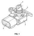
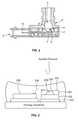
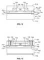
- FIG. 1is a perspective view of a packaged pressure sensor and FIG. 2 is a cross-section of the pressure sensor shown in FIG. 1 .
- the pressure sensoris comprised of a housing 2 that encloses a MEMS pressure sensing element 6 and an electronic circuit 7 . Fluid pressure including gases and liquids is applied through the pressure port 4 to the sensing element 6 , which is electrically connected with an electronic circuit 7 .
- Lead frame electrodes 10provide a means for electrical connections to be made with the electronic circuit 7 and the sensing element 6 .
- the electronic circuit 7 , MEMS pressure sensing element 6 , wires and wire bondsare located in a pocket 9 of the housing 2 .
- a gel 8fills the pocket 9 in the housing 2 and covers the electronic circuit 7 , MEMS pressure sensing element 6 , wires and wire bonds.
- the MEMS sensing element 6includes a piezoresistive bridge. The resistances of the piezoresistors in the bridge change with the applied pressure through the port 4 , and circuit 7 detects the resistance changes of the piezoresistive bridge and outputs an electrical signal through the lead frame 10 responding to the applied pressure signal.
- the gel 8protects the MEMS sensing element 6 , wires that extend from the sensing element 6 to the circuit 7 , from mechanical vibration and from moisture in the fluid (liquid or gas) that can build up the die (both IC and element) surfaces.
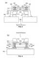
- the sensing element 6 shown in FIG. 2is a so called absolute pressure sensing element. As can be seen in the enlarged view of the sensing element 6 provided in FIG. 3 , the sensing element 6 is comprised of a silicon die 201 formed with a thin diaphragm 203 on which a piezoresistive bridge is built.
- the absolute pressure sensor as shown in FIGS. 1-3works well for many applications, however, corrosive gases and liquids that are commonly found in automotive exhaust gases or in other “harsh media” can degrade the conventional gel. When used to sense harsh media, the gel eventually deteriorates and fails to protect the lead wires 206 and bond pads 205 from reacting with the harsh media. The pressure sensor itself eventually fails.
- FIG. 1 and FIG. 2Another problem with gel used in prior art pressure sensors shown in FIG. 1 and FIG. 2 arises when the sensor is subjected to certain types of mechanical vibrations.
- the gelis bulky and massive.
- vibration of the geltransmits the vibration of a large mass to the diaphragm which in turn subjects the thin diaphragm to large acceleration forces. If the gel is caused to vibrate with a high acceleration and/or at a high frequency, the gel vibration can damage the diaphragm 203 .
- High frequency, high-acceleration vibrationoccurs when the cover 3 is ultrasonically welded to the housing 2 .
- FIG. 1is a perspective view of a prior art absolute pressure sensor
- FIG. 2is a cross-section of the sensor shown in FIG. 1 ;
- FIG. 3is a cross-section of a prior art for an absolute pressure sensor assembly
- FIG. 4-FIG . 7show cross-sections of the new absolute pressure sensing elements in four embodiments
- FIG. 8-FIG . 9show the flexible packaging approaches using the new absolute pressure sensing elements, a conventional wire bonding approach in FIG. 8 and a flip-chip surface mounting die attach in FIG. 9 ;
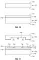
- FIG. 10-FIG . 16shown the major process steps for making the new absolute sensing elements
- FIG. 17is a cross-section of a packaged pressure sensor using the new sensing element that does not require gel in the second pocket.
- FIG. 18is a cross-section of an alternate embodiment of a packaged pressure sensor using a new sensing element, wherein the gel may be used but will not cause any issues to the sensing element.
- FIG. 4shows a cross-section of a preferred embodiment of a sensing element 300 , comprising two silicon die: a silicon cap or a cap 301 on the top and a device die or a silicon die 302 on the bottom.
- the cap 301is embedded with conductive vias 304 insulated from each other by a dielectric-filled cylindrical ring 305 surrounding each via 304 .
- the bottom side of the cap 301has a recess 307 formed into it.
- the top side of the cap 301is covered with a dielectric passivation layer 350 over which there are metal bond pads 306 electrically connected with the respective conductive vias 304 through the contact windows opened in the passivation layer 350 .
- the silicon die 302is comprised of two silicon layers: a thin, upper silicon layer 308 where the diaphragm 309 with edges 355 is formed, and a lower, thick silicon layer 310 where a cavity 311 having a substantially vertical wall 312 is formed.
- the cavity 311is formed to be located under the diaphragm 309 .
- the two silicon layers 308 and 310are attached to each other through an oxide layer 313 .
- the diaphragm 309is embedded with a piezoresistive bridge circuit 314 on the top side of the diaphragm 309 , which is the side opposite the cavity 311 .
- the piezoresistive bridge circuit 314 on the diaphragm 309comprises electrical components 332 that include silicon piezoresistors as well as conductive silicon interconnects 333 .
- the cap 301is hermetically sealed to the silicon die 302 through a thin silicon oxide layer 303 in such a way that the recess 307 in the cap 301 encloses an open volume in the cap 301 .
- the dimensions of the recess 307are such that the vertical walls of the recess 307 are located beyond the diaphragm edge 355 but inside the conductive vias 304 , which electrically connect interconnects 333 of the circuit 314 through the contact windows opened in the thin oxide layer 303 .
- the pressure inside the enclosed recess 307is preferably a vacuum, or at least in a partial vacuum so that diaphragm deflections are caused by a pressure to be measured.
- the capis formed or provided with a through-hole (not shown) that leads into the recess 307 , which enables the sensor to function as a differential pressure sensor.
- FIG. 5shows a cross-section of a second embodiment of a sensing element 400 .
- the sensing element 400 shown in FIG. 5differs from the sensing element 300 shown in FIG. 4 in that the cavity 411 shown in FIG. 5 is depicted as having a slopped wall 412 .
- the cavity 311has a substantially vertical wall 312 .
- FIG. 6shows a cross-section of a third embodiment of a sensing element 500 .
- the sensing element 500 shown in FIG. 6differs from the sensing element shown in FIG. 4 in that the cavity 411 in FIG. 6 has a sloped wall.
- the silicon die 502 in FIG. 6has only one silicon layer.
- FIG. 7shows a cross-section of a forth embodiment of a sensing element 600 .
- the sensing element 600has an extra pedestal 620 with a coincident hole 621 aligned to the cavity 611 formed in the silicon die 602 .
- the pedestal 620is attached to the cavity side of the element that is comprised of a cap 601 and a silicon die 602 .
- such a pedestal 620 with a hole 621can minimize the effects of the packaging stresses on the sensing element.
- the second pedestal 620 with a hole 621 depicted in FIG. 7can be optionally provided to each of the embodiments shown in FIGS. 4-6 .
- each circuit on the sensing element shown in FIGS. 4-7has more than one electrode or interconnect that is connected to a metal bond pad through a conductive via.
- the drawingsshow only two metal bond pads on top of conductive vias located on two sides of the die.
- the structures shown in the figurespermit the bond pads to be located at various different locations.
- the top surface of the cap dieis covered with a dielectric passivation layer, which is identified in FIG. 4 by reference numeral 350 , in FIG. 5 by reference numeral 450 , in FIG. 6 by reference numeral 550 , and in FIG. 7 by reference numeral 650 .
- the dielectric passivation layer(s)is/are comprised of silicon oxide and/or silicon nitride.
- the metal bond padscan be located anywhere on top of the passivation layer on the top side of the cap die.
- Metal interconnect linescan be formed on top of the passivation layer to electrically connect the bond pads with associated conductive vias through the contact windows opened in the passivation layer 350 , 450 , 550 or 650 as shown in FIGS. 4-7 .
- the metal bond padscan be located in different spots on top of the passivation layer on the cap die based on the special packaging demand, such as on the corners, or in one side of the die, or in two sides of the die, etc.
- FIG. 8shows a packaging structure for a sensing element identified by reference numeral 500 , the sensing element 500 being an exemplar of the one depicted in FIG. 6 , but also representative of the sensing elements 300 , 400 and 600 depicted in FIGS. 4 , 5 and 7 respectively.
- the sensing element 500is attached to a package substrate 540 having a hole 541 aligned with the cavity 511 of the element 500 .
- the sensing elementis attached to the substrate using a silicone mounting adhesive 530 .
- Wire bonding 520is used to electrically connect the bond pads 506 to metal pads on the package substrate 540 , or to an integrated circuit (IC) die (not shown), or to a printed circuit board or PCB (not shown).
- the aforementioned gel(not shown) is applied over the wire bond although the gel is not shown in FIG. 8 .
- the sensing elementis configured in FIG. 8 , i.e., with the working fluid applied to the diaphragm 509 through the hole 541 , the gel does not contact the diaphragm. Constructing the sensing element as described above and packaging it as shown in FIG. 8 avoids the problems that exist with prior art sensing elements having the wire bonds and diaphragms covered with gel.
- the packaging shown in FIG. 8is also compatible for use with harsh working fluid or media because the top surface of the circuit 514 having piezoresistive devices is sealed inside the recess 507 .
- Materials compatible with harsh mediaare used for the die mounting layer 530 , the diaphragm 509 and the cavity wall 512 .
- FIG. 9shows another way to package a sensing element in which the sensing element 500 is attached to a package substrate 540 using a ball grid array (BGA) 560 .
- the BGA 560is comprised of materials such as gold (Au) and tin (Sn), which are used to physically attach the sensing element 500 to the substrate 540 and to electrically connect metal bond pads 506 on the sensing element to metal pads 543 on the package substrate 540 .
- An under fill material 561is used to protect the BGA 560 from reacting with harsh media that the sensing element 500 might be exposed to.
- no wire bonding or gelare needed to electrically connect the piezoresistive circuit elements to other external electronic devices. Gel related issues that exist with prior art methods and structures are therefore eliminated.
- the method and structure shown in FIG. 9is usable with harsh media because the top surface of the circuit 514 having the piezoresistive circuit elements is sealed inside the recess 507 .
- Materials that are exposed to harsh mediainclude the underfill layer 561 and the silicon backside of the diaphragm 509 and the cavity wall 512 but those materials are selected to be harsh-media resistant.
- FIGS. 10-21show the steps to construct one sensing element structure, however, the process steps depicted in the figures and described below can be used to simultaneously fabricate hundreds or thousands of sensing elements depending on the designed die size and size of the wafer from which the die are obtained.
- the described method of making the new elementstherefore includes a wafer-level fabrication method.
- the top wafer 701is a simple silicon wafer, referred to as a cap wafer 701 . It has a top side 715 and a bottom side 716 .
- the bottom wafer 702is preferably a SOI wafer, and is referred to as the device wafer 702 . As with the top wafer 702 , the device wafer 702 has its own top side 717 and a bottom side 718 .
- the device wafer 702has two separate silicon layers one is a thin device layer 708 having its top surface as the top side 717 of the device wafer 702 .
- the other layeris a relatively thick carrier layer 710 , with its bottom surface being the bottom side 718 of the device wafer 702 .
- the thin device layer 708is used to fabricate circuits such as piezoresistive Wheatstone bridges.
- the thickness of the BOX layeris typically between about 0.5 to about 3 microns.
- the device wafer 702can also be a simple silicon wafer.
- the SOI waferis preferred however, because it enables using an etch stop in a diaphragm-forming step, and also enables a nearly vertical sidewall in the cavity under the diaphragm, one benefit of which is minimized die size.
- a first step of the methodis to form a recess 707 into the bottom side 716 of the cap wafer 701 .
- the depth of the recess 707is preferably between about 5 microns to about 20 microns.
- the recess 707has its own bottom surface 719 , which is preferably formed to be planar or substantially planar.
- the intersection of the horizontal bottom surface 719 of the recess 707 with the side walls 730 formed during the etching processdefines an outer perimeter 731 of the recess 707 .
- the device wafer 702is processed to form a circuit 714 such as the aforementioned piezoresistive bridge, on the top surface 717 of the device wafer 702 as shown in FIG. 11 .
- the circuit 714comprises components 732 such as the silicon piezoresistors, and conductive silicon interconnects 733 .
- the silicon conductive interconnects 733are used to electrically connect the piezoresistive components 732 to each other and form a useful circuit 714 such as a Wheatstone bridge, which is a circuit well-known to those of ordinary skill in the electronic arts.
- the top surface 717 of the device wafer 702is covered with a thin oxide layer. FIG.
- fusion bondingis a technique well known to those of ordinary skill in MEMS technology. The details of form a fusion bond are therefore omitted for brevity.
- the fusion bondjoins the bottom surface 716 of the cap wafer 701 and the top surface 717 of the device wafer 702 together through an oxide layer 703 .
- the cavity 707is large enough to enclose all the components 732 and silicon interconnects 733 .
- the cap wafer 701thus encloses and protects the circuit 714 .
- FIG. 13also shows the cross-section of the wafers when the conductive vias 704 and metal bond pads 706 are formed in such a way that the bottom ends of the vias 704 are electrically contacted with the respective conductive silicon interconnects 733 of the circuit 714 .
- the top ends of the vias 704are electrically connected to the metal bond pads 706 formed on top of a passivation layer 750 deposited on the top side 715 of the cap wafer 701 .
- the vias 704are formed in steps. First, a deep reactive ion etch (DRIE) is performed to form a hollow cylindrical ring 705 surround an area where a conductive via 704 will be formed later. The ring 705 is formed beginning from the top side 715 and ends at the oxide layer 703 .
- DRIEdeep reactive ion etch
- the next stepis to fill the rings 705 with dielectric materials such as silicon oxide and/or silicon nitride so that each silicon island surrounded by the ring 705 is electrically isolated from the rest of the cap wafer 701 .
- the third stepis to polish the top surface 715 of the cap wafer 705 .
- each silicon islandis surrounded by the isolation ring 705 .
- the holes etched inside each silicon islandstarts from the top surface 715 of the cap wafer 715 and ends at the top surface of the silicon conductive interconnects 733 of the circuit 714 .
- a forth step of forming the conductive viasis to fill the etched holes with conductive material, such as aluminum or conductive poly-silicon.
- conductive materialsuch as aluminum or conductive poly-silicon.
- the conductive material added to the etched holesform the conductive vias 704 .
- a fifth stepis to polish the top surface of the cap wafer and deposit a passivation layer such as silicon oxide and/or silicon nitride on the top surface 715 of the cap wafer 701 .
- the last stepwhich is also visible in FIG. 13 , is to open contact windows through the passivation layer 750 and form metal bond pads 706 on top of the passivation layer 750 and over the conductive vias 704 in such a way that each metal bond pad 706 is electrically connected to a respective conductive via 704 .
- the conductive viacan be provided by forming a through-hole through the wafer and coating the sidewall of the through-hole with an oxide. After the oxide is formed, the remaining open volume of the through-hole can be filled with a conductive material.
- the device wafer 702can be a simple silicon wafer.
- the process steps for forming the device wafer 702 that are described aboveare also performed on a SOI wafer.
- the next step of the fabrication processis to selectively etch a cavity into the bottom side 718 of the device wafer 702 in order to form a diaphragm 709 in such a way that the components 732 of the circuit 714 are located on the top side of the diaphragm 709 and close to the diaphragm edges 755 .
- a mask layer 751is applied to the bottom surface 718 to protect area that is not to be etched and to open or expose areas of the bottom side 718 of the device wafer 702 that are to be etched away.
- the mask layer 751preferably comprises silicon oxide, silicon nitride and a photoresist.
- the hole 711can be formed using a wet etch with potassium hydroxide (KOH) or a dry etch, such as deep reactive ion etch (DRIE). Since both techniques are well known to those of ordinary skill in the art, details of their procedures are omitted for brevity.
- KOHpotassium hydroxide
- DRIEdeep reactive ion etch
- FIG. 14shows a cross-section of the wafer with a cavity 711 formed by using a wet etch method.
- the sloped wall 712is a well-known characteristic of wet etching silicon using an etchant like KOH.
- the wall angleis about 54° relative to the horizontal bottom surface 718 when the device wafer 702 is a (100)-oriented silicon wafer.
- the wet etching rate of silicon oxideis much less than the etching rate of silicon. Therefore, when the etch front reaches to the BOX layer 713 , the etching process is essentially stopped due to a very slow etch rate of silicon oxide. Because the BOX layer 713 effectively stops the etching process, upon completion of the silicon etch, a silicon diaphragm 709 with its thickness and uniformity same as the ones of the thin device layer 708 , is obtained.
- the device wafercan also be a simple one layer silicon wafer, as shown in FIG. 6 .
- the thickness and uniformity of the diaphragm 509is mainly controlled by the etch time, which normally ends up with a large thickness and uniformity variation from die-to-die within a wafer and from wafer-to-wafer within a wafer lot.
- FIG. 15shows a cross-section of the wafers with a cavity 711 formed by using a dry etch method, such as DRIE.
- DRIEdry etch method
- the fabrication of the sensing elements 700 shown in both FIGS. 14 and 15are completed, and they are ready to be further assembled into a package, as described below.
- An optional step that can be added to meet some application requirementsis to attach a pedestal substrate 760 with a hole 761 to the bottom side 718 of the device wafer 702 in such a way that the hole 761 is aligned close to the center location of the cavity 711 of the device wafer 702 , as shown in FIG. 16 .
- the pedestal substrate 760is a boron silicate glass wafer, and an anodic bond is used to attach the pedestal substrate 760 to the device wafer 702 .
- the mask layer 751 as shown in FIG. 14needs to be removed to expose the silicon surface 718 before the anodic bond is formed.
- the pedestal substrate 760can be either one or more silicon wafers or one or more glass wafers, and an adhesive bond using materials such as frit glass or epoxy type adhesives is used to attach it onto the bottom surface 718 of the device wafer 702 .
- the mask layer 751 as shown in FIG. 14is optional to be removed or not before the adhesive bond.
- FIG. 17is a cross-section of a first embodiment of a pressure sensor 100 A.
- the pressure sensor 100 Ais comprised of a lower housing 102 with first and second compartments or “pockets” 104 and 106 .
- a housing cover 108is ultrasonically welded to the lower housing 102 to hermetically seal the pockets 104 and 106 except for a fluid inlet port 110 that provides a pathway for liquids or gases into the pocket 106 to allow the fluid to exert pressure on a MEMS pressure sensing element 10 A sealed into the second pocket 106 of the lower housing 102 .
- the second pocket 106is devoid of gel because there are no loose lead wires in the pocket 106 that require the protection provided by the gel.
- An integrated circuitwhich is an application specific IC or ASIC, is attached to the bottom of the second pocket 104 using an adhesive 118 .
- Lead wires 120extend from the ASIC 116 to the lead frame 112 .
- the lead frame 112carries signals between the ASIC 116 and the circuit 28 .
- the first pocket 104 of the lower housing 102is partially filled with a gel 122 to protect the lead frame wires 120 from vibration whereas the second pocket 106 is devoid of gel.
- the structure shown in FIG. 17is thus capable of being ultrasonically welded without having the high frequency sound waves damage the MEMS device as described above. Pressure changes in the port 110 are also detected more accurately by deflection of the diaphragm 30 due to the fact that there is no gel with an associated inertia caused by its mass.
- FIG. 18shows an alternate embodiment of a pressure sensor 100 B.
- the sensor 100 Bis comprised of a housing 109 with a pocket that accommodates a MEMS pressure sensor 10 B and an integrated circuit 116 .
- the pocketis sealed by a cover 103 that is ultrasonically welded to the housing 109 .
- the pressure port 111that allows fluid to exert pressure on the MEMS sensor 10 B is formed into the housing 109 .
- a gel 122is added to the pocket to protect lead wires 120 that extend from the bottom surface 38 of the silicon element 20 to an integrated circuit 116 .
- the gel 122Since the gel 122 is added to the side of the MEMS sensor 10 B away from the pressure port 111 , the gel 122 does not affect the responsiveness of the diaphragm 30 nor does ultrasonic welding the cover 103 to the housing 109 tend to damage the MEMS sensor 10 B.
- the MEMS device 10 Bis attached to a glass or silicon pedestal 46 having a top surface 48 and a bottom surface 50 .
- An anodic bonding, or adhesive bonding, or fusion bonding 52 between the top of the pedestal 48 and the top surface 24 of the die 22permanently joins the pedestal 46 and the MEMS pressure sensor 10 B to each other.
- a thru-hole 54is formed in the pedestal 46 by drilling or etching, etc.
- An adhesive 56 between the bottom surface 50 of the pedestal 46 and the housing 109provides a sealed pathway for fluids that pass through the port 111 in the housing 109 and exert pressure on the diaphragm 30 .
- the MEMS pressure sensor 10 Bdetects absolute pressure inside the port 111 .
- the bottom surface 16 of the silicon cap 12is provided with a dielectric layer (not visible) and a metal bond pad which is connected to the nearby second end 21 B of the conductive vias 20 through a contact window or opening in the dielectric layer, not shown in the figures.
- a conductive interconnect on the bottom surface 26 of the die 22which provides an electrical connection between the first end 21 A of the conductive via 20 and the transducer 28 formed into the surface of the diaphragm 30 .
- a complete circuit or signal pathwaytherefore exists between the piezoresistive transducer 28 formed on the diaphragm 20 and an ASIC 116 via the conductive vias, bond pads 40 , and the lead frames 112 and lead wires 120 .
- the metal bond pad 40is preferably embodied as a ball grid array or BGA.
- the metallic interconnects between the first end 21 A of the vias 20is preferably an electrically conductive adhesive or solder.
Landscapes
- Physics & Mathematics (AREA)
- General Physics & Mathematics (AREA)
- Chemical & Material Sciences (AREA)
- Analytical Chemistry (AREA)
- Measuring Fluid Pressure (AREA)
- Pressure Sensors (AREA)
Abstract
Description
Claims (23)
Priority Applications (2)
| Application Number | Priority Date | Filing Date | Title |
|---|---|---|---|
| US12/473,176US8215176B2 (en) | 2009-05-27 | 2009-05-27 | Pressure sensor for harsh media sensing and flexible packaging |
| DE102010028305ADE102010028305A1 (en) | 2009-05-27 | 2010-04-28 | Pressure sensor for detecting or measuring aggressive media and flexible accommodation or packaging |
Applications Claiming Priority (1)
| Application Number | Priority Date | Filing Date | Title |
|---|---|---|---|
| US12/473,176US8215176B2 (en) | 2009-05-27 | 2009-05-27 | Pressure sensor for harsh media sensing and flexible packaging |
Publications (2)
| Publication Number | Publication Date |
|---|---|
| US20100300207A1 US20100300207A1 (en) | 2010-12-02 |
| US8215176B2true US8215176B2 (en) | 2012-07-10 |
Family
ID=43218696
Family Applications (1)
| Application Number | Title | Priority Date | Filing Date |
|---|---|---|---|
| US12/473,176Active2030-11-26US8215176B2 (en) | 2009-05-27 | 2009-05-27 | Pressure sensor for harsh media sensing and flexible packaging |
Country Status (2)
| Country | Link |
|---|---|
| US (1) | US8215176B2 (en) |
| DE (1) | DE102010028305A1 (en) |
Cited By (31)
| Publication number | Priority date | Publication date | Assignee | Title |
|---|---|---|---|---|
| US20100044809A1 (en)* | 2008-08-21 | 2010-02-25 | S3C, Inc. | Sensor Device Packaging And Method |
| US20130137207A1 (en)* | 2009-03-03 | 2013-05-30 | S3C, Inc. | Media-compatible electrically isolated pressure sensor for high temperature applications |
| US20140076059A1 (en)* | 2012-09-14 | 2014-03-20 | Sensata Technologies, Inc. | Heremetically glass sealed pressure sensor |
| US20140076057A1 (en)* | 2012-09-14 | 2014-03-20 | Sensata Technologies, Inc. | Pressure Sensor |
| US8701496B1 (en) | 2013-02-27 | 2014-04-22 | Honeywell International Inc. | Systems and methods for a pressure sensor having a two layer die structure |
| US20150040675A1 (en)* | 2013-08-09 | 2015-02-12 | Continental Automotive Systems, Inc. | Absolute Pressure Sensor With Improved Bonding Boundary |
| US9116057B2 (en) | 2013-02-27 | 2015-08-25 | Honeywell International Inc. | Integrated reference vacuum pressure sensor with atomic layer deposition coated input port |
| DE102016203232A1 (en) | 2015-04-09 | 2016-10-13 | Continental Automotive Systems, Inc. | 3D stacked piezoresistive pressure sensor |
| US9506831B2 (en) | 2012-03-09 | 2016-11-29 | Epcos Ag | Micromechanical measuring element and method for producing a micromechanical measuring element |
| US20170023426A1 (en)* | 2014-04-04 | 2017-01-26 | Ando Lars Feyh | Membrane-Based Sensor and Method for Robust Manufacture of a Membrane-Based Sensor |
| US9638559B1 (en) | 2016-02-10 | 2017-05-02 | Sensata Technologies Inc. | System, devices and methods for measuring differential and absolute pressure utilizing two MEMS sense elements |
| US9823151B2 (en) | 2013-03-14 | 2017-11-21 | Trl Enterprises Llc. | Fully swept pressure sensor |
| US9945747B1 (en) | 2016-10-13 | 2018-04-17 | Honeywell International Inc. | Gel filled port pressure sensor for robust media sealing |
| US10151647B2 (en) | 2013-06-19 | 2018-12-11 | Honeywell International Inc. | Integrated SOI pressure sensor having silicon stress isolation member |
| US10215655B2 (en) | 2015-12-31 | 2019-02-26 | Honeywell International Inc. | Pressure sensor assembly |
| US20190078957A1 (en)* | 2017-09-08 | 2019-03-14 | Fuji Electric Co.,Ltd. | Pressure sensor device |
| US10323998B2 (en) | 2017-06-30 | 2019-06-18 | Sensata Technologies, Inc. | Fluid pressure sensor |
| US10345156B2 (en) | 2015-07-01 | 2019-07-09 | Sensata Technologies, Inc. | Temperature sensor and method for the production of a temperature sensor |
| CN110186596A (en)* | 2019-05-29 | 2019-08-30 | 南京元感微电子有限公司 | A kind of spring force snesor |
| US10428716B2 (en) | 2016-12-20 | 2019-10-01 | Sensata Technologies, Inc. | High-temperature exhaust sensor |
| US10488289B2 (en) | 2016-04-11 | 2019-11-26 | Sensata Technologies, Inc. | Pressure sensors with plugs for cold weather protection and methods for manufacturing the plugs |
| US10502641B2 (en) | 2017-05-18 | 2019-12-10 | Sensata Technologies, Inc. | Floating conductor housing |
| US10545064B2 (en) | 2017-05-04 | 2020-01-28 | Sensata Technologies, Inc. | Integrated pressure and temperature sensor |
| US20200031661A1 (en)* | 2018-07-24 | 2020-01-30 | Invensense, Inc. | Liquid proof pressure sensor |
| US10557770B2 (en) | 2017-09-14 | 2020-02-11 | Sensata Technologies, Inc. | Pressure sensor with improved strain gauge |
| US20200200633A1 (en)* | 2018-12-21 | 2020-06-25 | Robert Bosch Gmbh | Pressure-sensor assembly |
| US10724907B2 (en) | 2017-07-12 | 2020-07-28 | Sensata Technologies, Inc. | Pressure sensor element with glass barrier material configured for increased capacitive response |
| US10830653B2 (en)* | 2019-03-27 | 2020-11-10 | Honeywell International Inc. | Noninvasive blood pressure sensor |
| US10871413B2 (en) | 2016-04-20 | 2020-12-22 | Sensata Technologies, Inc. | Method of manufacturing a pressure sensor |
| US11047753B2 (en) | 2018-12-27 | 2021-06-29 | Therm-O-Disc, Incorporated | Pressure sensor assembly and method for manufacturing a pressure sensor assembly |
| US12180067B2 (en) | 2018-09-17 | 2024-12-31 | Invensense, Inc. | Sensor with integrated heater |
Families Citing this family (23)
| Publication number | Priority date | Publication date | Assignee | Title |
|---|---|---|---|---|
| US8245575B2 (en)* | 2009-12-08 | 2012-08-21 | Jen-Huang Albert Chiou | Pressure sensor device with breakwater to reduce protective gel vibration |
| US8191423B2 (en)* | 2010-03-29 | 2012-06-05 | Continental Automotive Systems, Inc. | Grooved structure for die-mount and media sealing |
| US8171800B1 (en)* | 2011-01-25 | 2012-05-08 | Continental Automotive Systems, Inc. | Differential pressure sensor using dual backside absolute pressure sensing |
| US8497148B2 (en)* | 2011-07-22 | 2013-07-30 | Taiwan Semiconductor Manufacturing Company, Ltd. | MEMS devices and methods of forming same |
| US8466523B2 (en)* | 2011-10-07 | 2013-06-18 | Continental Automotive Systems, Inc. | Differential pressure sensor device |
| JP5935352B2 (en)* | 2012-01-27 | 2016-06-15 | 富士電機株式会社 | Manufacturing method of physical quantity sensor having SON structure. |
| US8969978B2 (en) | 2012-04-27 | 2015-03-03 | Melexis Technologies Nv | TMAP sensor systems and methods for manufacturing those |
| US9200973B2 (en)* | 2012-06-28 | 2015-12-01 | Intel Corporation | Semiconductor package with air pressure sensor |
| DE102013003130B4 (en)* | 2013-02-23 | 2019-09-05 | Testo Ag | gauge |
| US20150143926A1 (en) | 2013-11-23 | 2015-05-28 | Silicon Microstructures, Inc. | Area-efficient pressure sensing device |
| CN105300593B (en)* | 2014-07-28 | 2018-12-28 | 恩智浦美国有限公司 | The semiconductor sensor arrangement of encapsulation with lid |
| FR3025879B1 (en)* | 2014-09-15 | 2018-03-02 | Valeo Equipements Electriques Moteur | MOTOR VEHICLE ULTRASOUND SENSOR FOR DISTANCE MEASUREMENT, PROCESS FOR PRODUCING THE SAME AND USE THEREOF |
| WO2016137027A1 (en)* | 2015-02-25 | 2016-09-01 | (주)파트론 | Pressure sensor package and manufacturing method thereof |
| AU2016307951B2 (en)* | 2015-08-14 | 2021-04-01 | Alcon Inc. | Ocular implant with pressure sensor and delivery system |
| DE102016203428B3 (en)* | 2016-03-02 | 2017-02-23 | Metallux Ag | pressure sensor |
| TWI628137B (en)* | 2017-02-08 | 2018-07-01 | 蘇州明皜傳感科技有限公司 | Microelectromechanical system device |
| DE102017129442A1 (en)* | 2017-12-11 | 2019-06-13 | Infineon Technologies Ag | Pressure measuring device |
| US10921207B2 (en)* | 2018-03-28 | 2021-02-16 | Veoneer Us Inc. | Sensor assembly with linear contacts |
| US20190391046A1 (en)* | 2018-06-22 | 2019-12-26 | Sensata Technologies, Inc. | First level package for pressure sensor module |
| US11333566B2 (en)* | 2018-09-06 | 2022-05-17 | Apple Inc. | Electronic device with an integrated pressure sensor |
| DE102019101325A1 (en)* | 2019-01-17 | 2020-07-23 | USound GmbH | Manufacturing process for multiple MEMS transducers |
| CN114323406A (en)* | 2021-12-30 | 2022-04-12 | 西安交通大学 | Pressure sensor chip based on flip-chip technology, packaging structure and preparation method |
| CN115014595A (en)* | 2022-06-21 | 2022-09-06 | 绍兴中芯集成电路制造股份有限公司 | Pressure sensor and preparation method thereof |
Citations (17)
| Publication number | Priority date | Publication date | Assignee | Title |
|---|---|---|---|---|
| US4399707A (en)* | 1981-02-04 | 1983-08-23 | Honeywell, Inc. | Stress sensitive semiconductor unit and housing means therefor |
| US4502335A (en)* | 1983-05-04 | 1985-03-05 | Honeywell Inc. | Fluid pressure transmitter assembly |
| US4665754A (en)* | 1985-04-08 | 1987-05-19 | Honeywell Inc. | Pressure transducer |
| US4763098A (en)* | 1985-04-08 | 1988-08-09 | Honeywell Inc. | Flip-chip pressure transducer |
| US5142912A (en)* | 1990-06-15 | 1992-09-01 | Honeywell Inc. | Semiconductor pressure sensor |
| US5259247A (en)* | 1991-02-28 | 1993-11-09 | Robert Bosch Gmbh | Sensor |
| US5684253A (en)* | 1997-01-08 | 1997-11-04 | Honeywell Inc. | Differential pressure sensor with stress reducing pressure balancing means |
| US5987921A (en)* | 1994-10-21 | 1999-11-23 | Fuji Electric Co., Ltd | Method for making a semiconductor acceleration sensor |
| US6255728B1 (en)* | 1999-01-15 | 2001-07-03 | Maxim Integrated Products, Inc. | Rigid encapsulation package for semiconductor devices |
| US6608370B1 (en) | 2002-01-28 | 2003-08-19 | Motorola, Inc. | Semiconductor wafer having a thin die and tethers and methods of making the same |
| US6878608B2 (en)* | 2001-05-31 | 2005-04-12 | International Business Machines Corporation | Method of manufacture of silicon based package |
| US7401525B2 (en)* | 2005-03-23 | 2008-07-22 | Honeywell International Inc. | Micro-machined pressure sensor with polymer diaphragm |
| US7518493B2 (en)* | 2005-12-01 | 2009-04-14 | Lv Sensors, Inc. | Integrated tire pressure sensor system |
| US7518234B1 (en)* | 2002-10-03 | 2009-04-14 | The United States Of America As Represented By The Administrator Of The National Aeronautics And Space Admistration | MEMS direct chip attach packaging methodologies and apparatuses for harsh environments |
| US7644625B2 (en)* | 2007-12-14 | 2010-01-12 | Honeywell International Inc. | Differential pressure sense die based on silicon piezoresistive technology |
| US7726197B2 (en)* | 2006-04-26 | 2010-06-01 | Honeywell International Inc. | Force sensor package and method of forming same |
| US7775119B1 (en) | 2009-03-03 | 2010-08-17 | S3C, Inc. | Media-compatible electrically isolated pressure sensor for high temperature applications |
- 2009
- 2009-05-27USUS12/473,176patent/US8215176B2/enactiveActive
- 2010
- 2010-04-28DEDE102010028305Apatent/DE102010028305A1/ennot_activeCeased
Patent Citations (17)
| Publication number | Priority date | Publication date | Assignee | Title |
|---|---|---|---|---|
| US4399707A (en)* | 1981-02-04 | 1983-08-23 | Honeywell, Inc. | Stress sensitive semiconductor unit and housing means therefor |
| US4502335A (en)* | 1983-05-04 | 1985-03-05 | Honeywell Inc. | Fluid pressure transmitter assembly |
| US4665754A (en)* | 1985-04-08 | 1987-05-19 | Honeywell Inc. | Pressure transducer |
| US4763098A (en)* | 1985-04-08 | 1988-08-09 | Honeywell Inc. | Flip-chip pressure transducer |
| US5142912A (en)* | 1990-06-15 | 1992-09-01 | Honeywell Inc. | Semiconductor pressure sensor |
| US5259247A (en)* | 1991-02-28 | 1993-11-09 | Robert Bosch Gmbh | Sensor |
| US5987921A (en)* | 1994-10-21 | 1999-11-23 | Fuji Electric Co., Ltd | Method for making a semiconductor acceleration sensor |
| US5684253A (en)* | 1997-01-08 | 1997-11-04 | Honeywell Inc. | Differential pressure sensor with stress reducing pressure balancing means |
| US6255728B1 (en)* | 1999-01-15 | 2001-07-03 | Maxim Integrated Products, Inc. | Rigid encapsulation package for semiconductor devices |
| US6878608B2 (en)* | 2001-05-31 | 2005-04-12 | International Business Machines Corporation | Method of manufacture of silicon based package |
| US6608370B1 (en) | 2002-01-28 | 2003-08-19 | Motorola, Inc. | Semiconductor wafer having a thin die and tethers and methods of making the same |
| US7518234B1 (en)* | 2002-10-03 | 2009-04-14 | The United States Of America As Represented By The Administrator Of The National Aeronautics And Space Admistration | MEMS direct chip attach packaging methodologies and apparatuses for harsh environments |
| US7401525B2 (en)* | 2005-03-23 | 2008-07-22 | Honeywell International Inc. | Micro-machined pressure sensor with polymer diaphragm |
| US7518493B2 (en)* | 2005-12-01 | 2009-04-14 | Lv Sensors, Inc. | Integrated tire pressure sensor system |
| US7726197B2 (en)* | 2006-04-26 | 2010-06-01 | Honeywell International Inc. | Force sensor package and method of forming same |
| US7644625B2 (en)* | 2007-12-14 | 2010-01-12 | Honeywell International Inc. | Differential pressure sense die based on silicon piezoresistive technology |
| US7775119B1 (en) | 2009-03-03 | 2010-08-17 | S3C, Inc. | Media-compatible electrically isolated pressure sensor for high temperature applications |
Cited By (45)
| Publication number | Priority date | Publication date | Assignee | Title |
|---|---|---|---|---|
| US8643127B2 (en) | 2008-08-21 | 2014-02-04 | S3C, Inc. | Sensor device packaging |
| US20100044809A1 (en)* | 2008-08-21 | 2010-02-25 | S3C, Inc. | Sensor Device Packaging And Method |
| US20130137207A1 (en)* | 2009-03-03 | 2013-05-30 | S3C, Inc. | Media-compatible electrically isolated pressure sensor for high temperature applications |
| US8627559B2 (en)* | 2009-03-03 | 2014-01-14 | S3C, Inc. | Media-compatible electrically isolated pressure sensor for high temperature applications |
| US9506831B2 (en) | 2012-03-09 | 2016-11-29 | Epcos Ag | Micromechanical measuring element and method for producing a micromechanical measuring element |
| US9027410B2 (en)* | 2012-09-14 | 2015-05-12 | Sensata Technologies, Inc. | Hermetically glass sealed pressure sensor |
| US8820170B2 (en)* | 2012-09-14 | 2014-09-02 | Sensata Technologies, Inc. | Pressure sensor |
| US20140076059A1 (en)* | 2012-09-14 | 2014-03-20 | Sensata Technologies, Inc. | Heremetically glass sealed pressure sensor |
| US20140076057A1 (en)* | 2012-09-14 | 2014-03-20 | Sensata Technologies, Inc. | Pressure Sensor |
| US8883536B2 (en) | 2013-02-27 | 2014-11-11 | Honeywell International Inc | Systems and methods for a pressure sensor having a two layer die structure |
| US9116057B2 (en) | 2013-02-27 | 2015-08-25 | Honeywell International Inc. | Integrated reference vacuum pressure sensor with atomic layer deposition coated input port |
| US8701496B1 (en) | 2013-02-27 | 2014-04-22 | Honeywell International Inc. | Systems and methods for a pressure sensor having a two layer die structure |
| US9823151B2 (en) | 2013-03-14 | 2017-11-21 | Trl Enterprises Llc. | Fully swept pressure sensor |
| US10151647B2 (en) | 2013-06-19 | 2018-12-11 | Honeywell International Inc. | Integrated SOI pressure sensor having silicon stress isolation member |
| US20150040675A1 (en)* | 2013-08-09 | 2015-02-12 | Continental Automotive Systems, Inc. | Absolute Pressure Sensor With Improved Bonding Boundary |
| US9546922B2 (en)* | 2013-08-09 | 2017-01-17 | Continental Automotive Systems, Inc. | Absolute pressure sensor with improved cap bonding boundary |
| US20170023426A1 (en)* | 2014-04-04 | 2017-01-26 | Ando Lars Feyh | Membrane-Based Sensor and Method for Robust Manufacture of a Membrane-Based Sensor |
| US11402288B2 (en)* | 2014-04-04 | 2022-08-02 | Robert Bosch Gmbh | Membrane-based sensor having a plurality of spacers extending from a cap layer |
| US9846095B2 (en) | 2015-04-09 | 2017-12-19 | Continental Automotive Systems, Inc. | 3D stacked piezoresistive pressure sensor |
| DE102016203232A1 (en) | 2015-04-09 | 2016-10-13 | Continental Automotive Systems, Inc. | 3D stacked piezoresistive pressure sensor |
| US10345156B2 (en) | 2015-07-01 | 2019-07-09 | Sensata Technologies, Inc. | Temperature sensor and method for the production of a temperature sensor |
| US10215655B2 (en) | 2015-12-31 | 2019-02-26 | Honeywell International Inc. | Pressure sensor assembly |
| US9638559B1 (en) | 2016-02-10 | 2017-05-02 | Sensata Technologies Inc. | System, devices and methods for measuring differential and absolute pressure utilizing two MEMS sense elements |
| EP3205995A1 (en) | 2016-02-10 | 2017-08-16 | Sensata Technologies, Inc. | System, devices and methods for measuring differential and absolute pressure utilitizing two mems sense elements |
| US10488289B2 (en) | 2016-04-11 | 2019-11-26 | Sensata Technologies, Inc. | Pressure sensors with plugs for cold weather protection and methods for manufacturing the plugs |
| US10871413B2 (en) | 2016-04-20 | 2020-12-22 | Sensata Technologies, Inc. | Method of manufacturing a pressure sensor |
| US9945747B1 (en) | 2016-10-13 | 2018-04-17 | Honeywell International Inc. | Gel filled port pressure sensor for robust media sealing |
| US10428716B2 (en) | 2016-12-20 | 2019-10-01 | Sensata Technologies, Inc. | High-temperature exhaust sensor |
| US11105698B2 (en) | 2017-05-04 | 2021-08-31 | Sensata Technologies, Inc. | Method of assembling a sensing device having a double clinch seal |
| US10545064B2 (en) | 2017-05-04 | 2020-01-28 | Sensata Technologies, Inc. | Integrated pressure and temperature sensor |
| US10502641B2 (en) | 2017-05-18 | 2019-12-10 | Sensata Technologies, Inc. | Floating conductor housing |
| US10323998B2 (en) | 2017-06-30 | 2019-06-18 | Sensata Technologies, Inc. | Fluid pressure sensor |
| US10969288B2 (en) | 2017-06-30 | 2021-04-06 | Sensata Technologies, Inc. | Fluid pressure sensor |
| US10724907B2 (en) | 2017-07-12 | 2020-07-28 | Sensata Technologies, Inc. | Pressure sensor element with glass barrier material configured for increased capacitive response |
| US10890502B2 (en)* | 2017-09-08 | 2021-01-12 | Fuji Electric Co., Ltd. | Pressure sensor device |
| US20190078957A1 (en)* | 2017-09-08 | 2019-03-14 | Fuji Electric Co.,Ltd. | Pressure sensor device |
| US10557770B2 (en) | 2017-09-14 | 2020-02-11 | Sensata Technologies, Inc. | Pressure sensor with improved strain gauge |
| US20200031661A1 (en)* | 2018-07-24 | 2020-01-30 | Invensense, Inc. | Liquid proof pressure sensor |
| US12180067B2 (en) | 2018-09-17 | 2024-12-31 | Invensense, Inc. | Sensor with integrated heater |
| US20200200633A1 (en)* | 2018-12-21 | 2020-06-25 | Robert Bosch Gmbh | Pressure-sensor assembly |
| US11307110B2 (en)* | 2018-12-21 | 2022-04-19 | Robert Bosch Gmbh | Pressure-sensor assembly having a carrier substrate |
| US11047753B2 (en) | 2018-12-27 | 2021-06-29 | Therm-O-Disc, Incorporated | Pressure sensor assembly and method for manufacturing a pressure sensor assembly |
| US10830653B2 (en)* | 2019-03-27 | 2020-11-10 | Honeywell International Inc. | Noninvasive blood pressure sensor |
| US11768116B2 (en) | 2019-03-27 | 2023-09-26 | Honeywell International Inc. | Noninvasive blood pressure sensor |
| CN110186596A (en)* | 2019-05-29 | 2019-08-30 | 南京元感微电子有限公司 | A kind of spring force snesor |
Also Published As
| Publication number | Publication date |
|---|---|
| US20100300207A1 (en) | 2010-12-02 |
| DE102010028305A1 (en) | 2011-08-25 |
Similar Documents
| Publication | Publication Date | Title |
|---|---|---|
| US8215176B2 (en) | Pressure sensor for harsh media sensing and flexible packaging | |
| US20230417614A1 (en) | Mems pressure sensor | |
| US6346742B1 (en) | Chip-scale packaged pressure sensor | |
| CN106052941B (en) | 3D Stacked Piezoresistive Pressure Sensor | |
| EP3394586B1 (en) | Stress-isolated absolute pressure sensor | |
| US8049326B2 (en) | Environment-resistant module, micropackage and methods of manufacturing same | |
| US10407299B2 (en) | 3D MEMS device with hermetic cavity | |
| US10656035B2 (en) | Piezoresistive sensor with spring flexures for stress isolation | |
| US9046546B2 (en) | Sensor device and related fabrication methods | |
| EP2481703B1 (en) | Sensor protection | |
| US6351996B1 (en) | Hermetic packaging for semiconductor pressure sensors | |
| US9926188B2 (en) | Sensor unit including a decoupling structure and manufacturing method therefor | |
| EP2189773B1 (en) | Design of wet/wet differential pressure sensor based on microelectronic packaging process | |
| CN100584741C (en) | Method for mounting semiconductor chips and corresponding semiconductor chip arrangement | |
| EP1853928A1 (en) | High performance mems packaging archetecture | |
| US10266392B2 (en) | Environment-resistant module, micropackage and methods of manufacturing same | |
| WO2020248466A1 (en) | Back hole lead type pressure sensor and manufacturing method therefor | |
| CN107892268B (en) | Pressure sensor and manufacturing method thereof | |
| US20170057810A1 (en) | Strain Reduction and Sensing on Package Substrates | |
| JP2007240250A (en) | Pressure sensor, pressure sensor package, pressure sensor module, and electronic component | |
| CN102336390B (en) | Microelectromechanical structure with pressure sensor and method of manufacturing the same | |
| CN210084937U (en) | Back hole lead wire type pressure sensor | |
| CN207456650U (en) | Pressure sensor | |
| CN113443602A (en) | Wafer level packaging structure of micro electro mechanical system chip and manufacturing process thereof |
Legal Events
| Date | Code | Title | Description |
|---|---|---|---|
| AS | Assignment | Owner name:TEMIC AUTOMOTIVE OF NORTH AMERICA, INC., ILLINOIS Free format text:ASSIGNMENT OF ASSIGNORS INTEREST;ASSIGNORS:DING, XIAOYI;FRYE, JEFFREY J.;CHIOU, JEN-HUANG ALBERT;SIGNING DATES FROM 20090807 TO 20090810;REEL/FRAME:023073/0376 | |
| AS | Assignment | Owner name:CONTINENTAL AUTOMOTIVE SYSTEMS, INC., MICHIGAN Free format text:MERGER;ASSIGNOR:TEMIC AUTOMOTIVE OF NORTH AMERICA, INC.;REEL/FRAME:027654/0455 Effective date:20091210 | |
| STCF | Information on status: patent grant | Free format text:PATENTED CASE | |
| FEPP | Fee payment procedure | Free format text:PAYOR NUMBER ASSIGNED (ORIGINAL EVENT CODE: ASPN); ENTITY STATUS OF PATENT OWNER: LARGE ENTITY | |
| FPAY | Fee payment | Year of fee payment:4 | |
| MAFP | Maintenance fee payment | Free format text:PAYMENT OF MAINTENANCE FEE, 8TH YEAR, LARGE ENTITY (ORIGINAL EVENT CODE: M1552); ENTITY STATUS OF PATENT OWNER: LARGE ENTITY Year of fee payment:8 | |
| AS | Assignment | Owner name:VITESCO TECHNOLOGIES USA, LLC., MICHIGAN Free format text:ASSIGNMENT OF ASSIGNORS INTEREST;ASSIGNOR:CONTINENTAL AUTOMOTIVE SYSTEMS, INC.;REEL/FRAME:057650/0891 Effective date:20210810 | |
| MAFP | Maintenance fee payment | Free format text:PAYMENT OF MAINTENANCE FEE, 12TH YEAR, LARGE ENTITY (ORIGINAL EVENT CODE: M1553); ENTITY STATUS OF PATENT OWNER: LARGE ENTITY Year of fee payment:12 |