US8212139B2 - Thin-film photovoltaic module - Google Patents
Thin-film photovoltaic moduleDownload PDFInfo
- Publication number
- US8212139B2 US8212139B2US12/684,595US68459510AUS8212139B2US 8212139 B2US8212139 B2US 8212139B2US 68459510 AUS68459510 AUS 68459510AUS 8212139 B2US8212139 B2US 8212139B2
- Authority
- US
- United States
- Prior art keywords
- strips
- strip
- thin
- module
- conductive
- Prior art date
- Legal status (The legal status is an assumption and is not a legal conclusion. Google has not performed a legal analysis and makes no representation as to the accuracy of the status listed.)
- Active, expires
Links
- 239000010409thin filmSubstances0.000titleclaimsabstractdescription74
- 239000000463materialSubstances0.000claimsabstractdescription137
- 239000010408filmSubstances0.000claimsabstractdescription48
- 238000006243chemical reactionMethods0.000claimsdescription68
- 239000000758substrateSubstances0.000claimsdescription29
- 230000001143conditioned effectEffects0.000claimsdescription19
- 229910052751metalInorganic materials0.000claimsdescription13
- 239000002184metalSubstances0.000claimsdescription13
- 238000004519manufacturing processMethods0.000claimsdescription12
- 239000000853adhesiveSubstances0.000claimsdescription11
- 230000001070adhesive effectEffects0.000claimsdescription11
- 239000004020conductorSubstances0.000claimsdescription11
- 229920000139polyethylene terephthalatePolymers0.000claimsdescription9
- 239000005020polyethylene terephthalateSubstances0.000claimsdescription9
- 229910052782aluminiumInorganic materials0.000claimsdescription8
- XAGFODPZIPBFFR-UHFFFAOYSA-NaluminiumChemical compound[Al]XAGFODPZIPBFFR-UHFFFAOYSA-N0.000claimsdescription8
- 230000004888barrier functionEffects0.000claimsdescription8
- RYGMFSIKBFXOCR-UHFFFAOYSA-NCopperChemical compound[Cu]RYGMFSIKBFXOCR-UHFFFAOYSA-N0.000claimsdescription7
- ATJFFYVFTNAWJD-UHFFFAOYSA-NTinChemical compound[Sn]ATJFFYVFTNAWJD-UHFFFAOYSA-N0.000claimsdescription7
- 229910052802copperInorganic materials0.000claimsdescription7
- 239000010949copperSubstances0.000claimsdescription7
- 229910052718tinInorganic materials0.000claimsdescription7
- PXHVJJICTQNCMI-UHFFFAOYSA-NNickelChemical compound[Ni]PXHVJJICTQNCMI-UHFFFAOYSA-N0.000claimsdescription6
- 238000002955isolationMethods0.000claimsdescription5
- -1polyethylene terephthalatePolymers0.000claimsdescription5
- 239000011135tinSubstances0.000claimsdescription5
- 239000004593EpoxySubstances0.000claimsdescription4
- 229920003229poly(methyl methacrylate)Polymers0.000claimsdescription4
- 239000004926polymethyl methacrylateSubstances0.000claimsdescription4
- 229910052709silverInorganic materials0.000claimsdescription4
- 239000004332silverSubstances0.000claimsdescription4
- 239000003190viscoelastic substanceSubstances0.000claimsdescription4
- BQCADISMDOOEFD-UHFFFAOYSA-NSilverChemical compound[Ag]BQCADISMDOOEFD-UHFFFAOYSA-N0.000claimsdescription3
- 239000011248coating agentSubstances0.000claimsdescription3
- 238000000576coating methodMethods0.000claimsdescription3
- PCHJSUWPFVWCPO-UHFFFAOYSA-NgoldChemical compound[Au]PCHJSUWPFVWCPO-UHFFFAOYSA-N0.000claimsdescription3
- 229910052737goldInorganic materials0.000claimsdescription3
- 239000010931goldSubstances0.000claimsdescription3
- 229910052759nickelInorganic materials0.000claimsdescription3
- 239000010935stainless steelSubstances0.000claimsdescription3
- 229910001220stainless steelInorganic materials0.000claimsdescription3
- 229910001209Low-carbon steelInorganic materials0.000claimsdescription2
- 239000011370conductive nanoparticleSubstances0.000claimsdescription2
- 239000012777electrically insulating materialSubstances0.000claims2
- 229910052755nonmetalInorganic materials0.000claims1
- 239000010410layerSubstances0.000description377
- 238000000034methodMethods0.000description40
- 239000012790adhesive layerSubstances0.000description29
- 238000009434installationMethods0.000description25
- 238000009432framingMethods0.000description20
- 238000012360testing methodMethods0.000description11
- URYYVOIYTNXXBN-OWOJBTEDSA-Ntrans-cycloocteneChemical compoundC1CCC\C=C\CC1URYYVOIYTNXXBN-OWOJBTEDSA-N0.000description11
- 230000007547defectEffects0.000description10
- 238000005520cutting processMethods0.000description9
- 238000005286illuminationMethods0.000description9
- XUIMIQQOPSSXEZ-UHFFFAOYSA-NSiliconChemical compound[Si]XUIMIQQOPSSXEZ-UHFFFAOYSA-N0.000description7
- 230000008901benefitEffects0.000description7
- 238000001816coolingMethods0.000description7
- 230000006870functionEffects0.000description7
- 239000000565sealantSubstances0.000description7
- 229910052710siliconInorganic materials0.000description7
- 239000010703siliconSubstances0.000description7
- 230000015572biosynthetic processEffects0.000description6
- 238000005516engineering processMethods0.000description6
- 238000010030laminatingMethods0.000description6
- 230000008569processEffects0.000description6
- 238000012545processingMethods0.000description6
- 238000005259measurementMethods0.000description5
- 238000003860storageMethods0.000description5
- 239000012141concentrateSubstances0.000description4
- 239000000839emulsionSubstances0.000description4
- 239000005038ethylene vinyl acetateSubstances0.000description4
- 238000011068loading methodMethods0.000description4
- 230000036961partial effectEffects0.000description4
- 229920003023plasticPolymers0.000description4
- 239000004033plasticSubstances0.000description4
- 229920001200poly(ethylene-vinyl acetate)Polymers0.000description4
- 238000007789sealingMethods0.000description4
- XLYOFNOQVPJJNP-UHFFFAOYSA-NwaterSubstancesOXLYOFNOQVPJJNP-UHFFFAOYSA-N0.000description4
- 238000003466weldingMethods0.000description4
- 230000005540biological transmissionEffects0.000description3
- 238000012423maintenanceMethods0.000description3
- 230000035515penetrationEffects0.000description3
- 230000002829reductive effectEffects0.000description3
- 230000003068static effectEffects0.000description3
- CURLTUGMZLYLDI-UHFFFAOYSA-NCarbon dioxideChemical compoundO=C=OCURLTUGMZLYLDI-UHFFFAOYSA-N0.000description2
- KTSFMFGEAAANTF-UHFFFAOYSA-N[Cu].[Se].[Se].[In]Chemical compound[Cu].[Se].[Se].[In]KTSFMFGEAAANTF-UHFFFAOYSA-N0.000description2
- 229910021417amorphous siliconInorganic materials0.000description2
- 238000004458analytical methodMethods0.000description2
- 238000005452bendingMethods0.000description2
- 230000000295complement effectEffects0.000description2
- 230000002950deficientEffects0.000description2
- 230000000694effectsEffects0.000description2
- 239000000835fiberSubstances0.000description2
- 239000000945fillerSubstances0.000description2
- 239000011521glassSubstances0.000description2
- 238000009413insulationMethods0.000description2
- 238000003475laminationMethods0.000description2
- 230000000670limiting effectEffects0.000description2
- 239000002245particleSubstances0.000description2
- 230000000737periodic effectEffects0.000description2
- 229920001343polytetrafluoroethylenePolymers0.000description2
- 239000004810polytetrafluoroethyleneSubstances0.000description2
- 238000007650screen-printingMethods0.000description2
- 238000000926separation methodMethods0.000description2
- 229910000679solderInorganic materials0.000description2
- 239000007787solidSubstances0.000description2
- GYHNNYVSQQEPJS-UHFFFAOYSA-NGalliumChemical compound[Ga]GYHNNYVSQQEPJS-UHFFFAOYSA-N0.000description1
- 239000004642PolyimideSubstances0.000description1
- 241000269913Pseudopleuronectes americanusSpecies0.000description1
- 238000002679ablationMethods0.000description1
- 230000003213activating effectEffects0.000description1
- 238000005219brazingMethods0.000description1
- DQXBYHZEEUGOBF-UHFFFAOYSA-Nbut-3-enoic acid;etheneChemical compoundC=C.OC(=O)CC=CDQXBYHZEEUGOBF-UHFFFAOYSA-N0.000description1
- 229910002092carbon dioxideInorganic materials0.000description1
- 239000001569carbon dioxideSubstances0.000description1
- 238000005266castingMethods0.000description1
- 238000005253claddingMethods0.000description1
- 238000004140cleaningMethods0.000description1
- 238000004891communicationMethods0.000description1
- 238000011109contaminationMethods0.000description1
- HVMJUDPAXRRVQO-UHFFFAOYSA-Ncopper indiumChemical compound[Cu].[In]HVMJUDPAXRRVQO-UHFFFAOYSA-N0.000description1
- 238000013016dampingMethods0.000description1
- 238000000151depositionMethods0.000description1
- 239000002274desiccantSubstances0.000description1
- 238000010586diagramMethods0.000description1
- 239000003989dielectric materialSubstances0.000description1
- 238000009792diffusion processMethods0.000description1
- 238000005553drillingMethods0.000description1
- 230000005611electricityEffects0.000description1
- 238000005538encapsulationMethods0.000description1
- 230000007613environmental effectEffects0.000description1
- 125000003700epoxy groupChemical group0.000description1
- 229910052733galliumInorganic materials0.000description1
- 230000017525heat dissipationEffects0.000description1
- 238000010438heat treatmentMethods0.000description1
- 230000007062hydrolysisEffects0.000description1
- 238000006460hydrolysis reactionMethods0.000description1
- 230000006872improvementEffects0.000description1
- 229910052738indiumInorganic materials0.000description1
- APFVFJFRJDLVQX-UHFFFAOYSA-Nindium atomChemical compound[In]APFVFJFRJDLVQX-UHFFFAOYSA-N0.000description1
- 238000003698laser cuttingMethods0.000description1
- 239000007769metal materialSubstances0.000description1
- 238000012544monitoring processMethods0.000description1
- 230000003287optical effectEffects0.000description1
- 239000011368organic materialSubstances0.000description1
- 230000003071parasitic effectEffects0.000description1
- 239000002985plastic filmSubstances0.000description1
- 229920006255plastic filmPolymers0.000description1
- 229920000647polyepoxidePolymers0.000description1
- 229920001721polyimidePolymers0.000description1
- 229920001296polysiloxanePolymers0.000description1
- 239000011253protective coatingSubstances0.000description1
- 230000001681protective effectEffects0.000description1
- 238000003908quality control methodMethods0.000description1
- 230000000191radiation effectEffects0.000description1
- 230000004044responseEffects0.000description1
- 238000005096rolling processMethods0.000description1
- 239000003566sealing materialSubstances0.000description1
- JNMWHTHYDQTDQZ-UHFFFAOYSA-Nselenium sulfideChemical compoundS=[Se]=SJNMWHTHYDQTDQZ-UHFFFAOYSA-N0.000description1
- 238000007493shaping processMethods0.000description1
- 238000002791soakingMethods0.000description1
- 238000005476solderingMethods0.000description1
- 239000000126substanceSubstances0.000description1
- 238000009827uniform distributionMethods0.000description1
- 238000009423ventilationMethods0.000description1
Images


Classifications
- H—ELECTRICITY
- H10—SEMICONDUCTOR DEVICES; ELECTRIC SOLID-STATE DEVICES NOT OTHERWISE PROVIDED FOR
- H10F—INORGANIC SEMICONDUCTOR DEVICES SENSITIVE TO INFRARED RADIATION, LIGHT, ELECTROMAGNETIC RADIATION OF SHORTER WAVELENGTH OR CORPUSCULAR RADIATION
- H10F19/00—Integrated devices, or assemblies of multiple devices, comprising at least one photovoltaic cell covered by group H10F10/00, e.g. photovoltaic modules
- H10F19/80—Encapsulations or containers for integrated devices, or assemblies of multiple devices, having photovoltaic cells
- H—ELECTRICITY
- H02—GENERATION; CONVERSION OR DISTRIBUTION OF ELECTRIC POWER
- H02S—GENERATION OF ELECTRIC POWER BY CONVERSION OF INFRARED RADIATION, VISIBLE LIGHT OR ULTRAVIOLET LIGHT, e.g. USING PHOTOVOLTAIC [PV] MODULES
- H02S40/00—Components or accessories in combination with PV modules, not provided for in groups H02S10/00 - H02S30/00
- H02S40/30—Electrical components
- H02S40/36—Electrical components characterised by special electrical interconnection means between two or more PV modules, e.g. electrical module-to-module connection
- H—ELECTRICITY
- H10—SEMICONDUCTOR DEVICES; ELECTRIC SOLID-STATE DEVICES NOT OTHERWISE PROVIDED FOR
- H10F—INORGANIC SEMICONDUCTOR DEVICES SENSITIVE TO INFRARED RADIATION, LIGHT, ELECTROMAGNETIC RADIATION OF SHORTER WAVELENGTH OR CORPUSCULAR RADIATION
- H10F19/00—Integrated devices, or assemblies of multiple devices, comprising at least one photovoltaic cell covered by group H10F10/00, e.g. photovoltaic modules
- H10F19/90—Structures for connecting between photovoltaic cells, e.g. interconnections or insulating spacers
- H10F19/902—Structures for connecting between photovoltaic cells, e.g. interconnections or insulating spacers for series or parallel connection of photovoltaic cells
- H10F19/904—Structures for connecting between photovoltaic cells, e.g. interconnections or insulating spacers for series or parallel connection of photovoltaic cells characterised by the shapes of the structures
- H—ELECTRICITY
- H10—SEMICONDUCTOR DEVICES; ELECTRIC SOLID-STATE DEVICES NOT OTHERWISE PROVIDED FOR
- H10F—INORGANIC SEMICONDUCTOR DEVICES SENSITIVE TO INFRARED RADIATION, LIGHT, ELECTROMAGNETIC RADIATION OF SHORTER WAVELENGTH OR CORPUSCULAR RADIATION
- H10F77/00—Constructional details of devices covered by this subclass
- H10F77/40—Optical elements or arrangements
- H10F77/42—Optical elements or arrangements directly associated or integrated with photovoltaic cells, e.g. light-reflecting means or light-concentrating means
- H10F77/488—Reflecting light-concentrating means, e.g. parabolic mirrors or concentrators using total internal reflection
- Y—GENERAL TAGGING OF NEW TECHNOLOGICAL DEVELOPMENTS; GENERAL TAGGING OF CROSS-SECTIONAL TECHNOLOGIES SPANNING OVER SEVERAL SECTIONS OF THE IPC; TECHNICAL SUBJECTS COVERED BY FORMER USPC CROSS-REFERENCE ART COLLECTIONS [XRACs] AND DIGESTS
- Y02—TECHNOLOGIES OR APPLICATIONS FOR MITIGATION OR ADAPTATION AGAINST CLIMATE CHANGE
- Y02E—REDUCTION OF GREENHOUSE GAS [GHG] EMISSIONS, RELATED TO ENERGY GENERATION, TRANSMISSION OR DISTRIBUTION
- Y02E10/00—Energy generation through renewable energy sources
- Y02E10/50—Photovoltaic [PV] energy
- Y02E10/52—PV systems with concentrators
Definitions
- the present inventionrelates generally to photovoltaic (“PV”) modules. More particularly, some example embodiments relate to PV modules made from thin-film PV materials.
- solar collectorsThere are two main types of solar collectors, including silicon and thin films, commonly used in PV modules, the solar collectors commonly composed of PV cells.
- Siliconis currently the predominant technology, and can generally be implemented as monocrystalline or polycrystalline cells encapsulated behind a transparent glass front plate.
- Thin-film technologyis not as wide-spread as the silicon technology due to its reduced efficiency, but it is gaining in popularity due to its lower cost.
- Thin-film materialsinclude amorphous, tandem or other silicon based thin-film materials, as well as copper indium gallium selenide (“CIGS”), copper indium gallium sulfur-selenide (“CIGSS”), and other materials. Thin-film materials can be produced in manufacturing quantities on glass substrates, metal substrates, or plastic films. Yields and efficiencies vary by technology, manufacturer, and substrate choice.
- example embodiments of the inventionrelate to PV modules made from thin-film PV materials.
- a PV modulein one example embodiment, includes an active layer, a top layer, and a bottom layer.
- the active layerincludes a plurality of strips of thin-film PV material that are arranged spaced apart from and substantially parallel to each other.
- the top layeris disposed above the active layer and includes a substantially transparent film.
- the bottom layeris disposed below the active layer, the bottom layer including a conductive backsheet configured to form a current return path for the strips of thin-film PV material.
- the PV modulefurther includes means for serially and redundantly interconnecting the strips of thin-film PV material together.
- a method of forming a longitudinally continuous PV moduleincludes arranging a plurality of strips of thin-film PV material to be spaced apart from and substantially parallel to each other.
- a bottom layeris laminated to a first surface of the plurality of strips of thin-film PV material, the bottom layer including a plurality of bottom layer conductive strips.
- a top layeris laminated to a second surface of the plurality of strips of thin-film PV material, the top layer including a plurality of top layer conductive strips.
- the lamination of the bottom layer to the first surface and the top layer to the second surfaceincludes serially and redundantly interconnecting the plurality of strips of thin-film PV material together by connecting each one of the strips of thin-film PV material to a different one of the plurality of bottom layer conductive strips and a different one of the plurality of top layer conductive strips.
- a computer-readable storage mediumhas computer-executable instructions stored thereon that, if executed by a computing device, cause the computing device to perform a method.
- the methodincludes receiving data indicating an installation angle for a PV module at an installation site, the PV module including a plurality of plastically deformable reflector regions and a plurality of longitudinally continuous strips of thin-film photovoltaic material. Data indicating a direction the installation site faces, a latitude of the installation site and elastic and visco-elastic bend relaxation parameters for the PV module is received. A shape for the plurality of plastically deformable reflector regions is determined based on the received data.
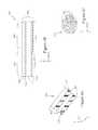
- FIGS. 1A-1Ddisclose aspects of an example flat PV module including flat interconnecting regions and PV regions of PV strips;
- FIGS. 2A-2Bdisclose aspects of an example corrugated PV module including shaped interconnecting regions
- FIGS. 3A-3Billustrate a first example top layer that may be implemented in the PV modules according to some embodiments
- FIGS. 4A-4Cillustrate a second example top layer that may be implemented in the PV modules according to some embodiments
- FIG. 5depicts an example PV module that implements top layer conductive strips without a power collection macro or nano grid for collecting power
- FIG. 6discloses a process flow for forming PV strips from a continuous sheet of PV material
- FIGS. 7A-7Billustrate an example PV module that implements bottom layer conductive strips and gimbal strips without top layer conductive strips to serially and redundantly interconnect PV strips;
- FIGS. 8A-8Billustrate an example PV module that implements bottom layer conductive strips and stitched contact strips without top layer conductive strips to serially and redundantly interconnect PV strips;
- FIG. 9depicts an example electronic circuit layer and power conversion circuits that can be implemented in the PV modules according to some embodiments.
- FIGS. 10A-10Cdisclose various PV modules electronics configurations
- FIGS. 11A-11Fdisclose various PV module mounting configurations
- FIGS. 12A-12Billustrate an example PV module with built-in fastener regions
- FIG. 13illustrates a roof-mounted PV module that implements passive cooling
- FIG. 14depicts a support device that can be implemented to support loads on a PV module
- FIGS. 15A-15Cdepict a PV module implementing discrete straps to support cross-directional loads on the PV module
- FIGS. 16A-16Bdepict incoming summer and winter light rays for static horizontally and vertically oriented PV modules with concentrators
- FIG. 17illustrates a PV module having PV strips of unequal width
- FIGS. 18A-18Ddisclose aspects of PV module having clip-on power conversion circuits
- FIGS. 19A-19Bdepicts methods and systems for roll-forming PV modules from continuous sheets of PV material
- FIGS. 20A and 20Billustrate additional details regarding the formation of PV modules from continuous sheets of PV material.
- FIGS. 21A-21Bdisclose a system for performing product testing on a sheet of PV module material formed according to the methods of FIGS. 19A and 19B .
- Example embodimentsgenerally relate to longitudinally continuous PV modules including an active layer having a plurality of longitudinally continuous PV strips, a flexible top layer disposed above the active layer, and a flexible bottom layer disposed below the active layer.
- PV modulescan include a plurality of conductive strips interposed between the PV strips that at least partially serially and redundantly interconnect the PV strips.
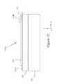
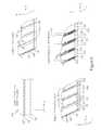
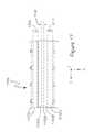
- FIG. 1Adepicts an perspective view of the PV module 100 .
- the PV module 100includes a plurality of active regions 102 , a plurality of interconnecting regions 104 , and lengthwise edge caps 106 A, 106 B (collectively “edge caps 106 ”).
- the active regions 102generally include PV material configured to convert solar energy into electricity by the photovoltaic effect.
- the interconnecting regions 104are configured to serially and redundantly interconnect the active regions 102 together. In some embodiments, the interconnecting regions 104 and active regions 104 at least partially overlap each other in the arbitrarily defined x-direction. Further, although the interconnecting regions 104 are depicted in FIG. 1A as being wider in the x-direction than the active regions 102 , in other embodiments the interconnecting regions 104 are narrower in the x-direction than the active regions 102 .
- some embodimentsinclude PV modules 100 with interconnecting regions 104 that are infinitesimally narrow in the x-direction, at least at the positive z surface of the PV module 100 , such that the positive z surface of the PV module 100 is made up substantially entirely of active regions 104 .
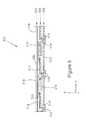
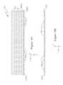
- FIG. 1Bdepicts an exploded perspective view of a portion of the PV module 100 .
- the PV module 100includes active regions 102 and interconnecting regions 104 . Further, the PV module 100 generally includes a top layer 108 , an active layer 110 , and a bottom layer 112 .
- the top layer 108includes a substantially transparent film 114 and a plurality of top layer conductive strips 116 A- 116 C (collectively “top layer conductive strips 116 ”) that are laminated or otherwise secured to a bottom surface of the top layer 108 .
- a top adhesive layer 118secures the top layer conductive strips 116 to the bottom surface of the top layer 108 .
- a power collection grid including one or more regions 120 A, 120 B(collectively “power collection grid 120 ”) is formed on a bottom surface of the substantially transparent film 114 .
- the top layer conductive strips 116provide mechanical stiffness to the PV module 100 and/or reduce the percentage of PV material in the PV module 100 .
- the top layer conductive strips 116are formed into concentrators to reflect and concentrate light onto the areas of PV material, for example.
- the active layer 110includes a plurality of strips of PV material 122 A- 122 B (collectively “PV strips 122 ”) that are longitudinally continuous and substantially flexible in some embodiments.
- PV strips 122are longitudinally continuous and substantially flexible in some embodiments.
- the term “longitudinally continuous” as applied to the PV strips 122means that the PV strips 122 are continuous along the length, e.g., in the arbitrarily-defined y-direction, of the PV strips 122 , as opposed to being divided into multiple discrete solar cells.
- the manufacturing process of the PV module 100in some embodiments involves manufacturing a longitudinally continuous sheet having multiple layers such as those depicted in FIG. 1B all laminated together.
- the longitudinally continuous sheetmay be up to 2000 feet or more in length, e.g., in the y-direction, and rolled up for ease of shipment.
- the longitudinally continuous sheetmay be sectioned into intermediate-sized sections and shipped in smaller rolls or stacked one on top of another.
- the longitudinally continuous sheet or the intermediate-sized sheetsmay be sectioned into finished lengths appropriate for installation before being shipped and/or at the installation site.
- the length in the y-direction of a finished PV module 100 suitable for installationis in a range from 20 feet to 40 feet, or even less than 20 feet or greater than 40 feet.
- the aspect ratio of a finished PV module 100is in a range from 6 to 50, or even less than 6 or greater than 50.
- the width (e.g., in the x-direction) of the PV module 100is in a range from 1 foot to 4 feet, or even less than 1 foot or greater than 4 feet.
- each of PV strips 122is between 0.5 inches and 6 inches wide as measured in the x-direction. In other embodiments, PV strips 122 are less than 0.5 inches wide or greater than 6 inches wide. Alternately or additionally, each PV module 100 includes anywhere from 10 to 40 PV strips 122 . In other embodiments, each PV module 100 includes fewer than 10 PV strips 122 or more than 40 PV strips 122 .
- the PV strip 122 Ais a thin-film PV material such as copper indium gallium selenide (“CIGS”), amorphous silicon (“a-Si”), or the like or any combination thereof.
- FIG. 1Cis a cross-sectional view of the PV strip 122 A according to some embodiments in which the PV strip 122 A is a thin-film PV material.
- the other PV strips 122 of PV module 100may be similarly configured to PV strip 122 A.
- the PV strip 122 Aincludes a substrate 124 , a thin-film active layer 126 and a transparent conducting oxide (“TCO”) 128 .
- TCOtransparent conducting oxide
- the PV strips 122 A- 122 B included in the PV module 100 and other PV modules according to some embodimentscan be manufactured using any method(s) and/or material(s) now known or later developed.
- the PV strip 122 Afurther includes one or more TCO-free regions 130 A, 130 B (collectively “regions 130 ”) and one or more isolation strips 132 .
- the regions 130are processing artifacts resulting from the formation of multiple PV strips 122 from a continuous sheet of thin-film PV material.
- the TCO 128is ablated from the continuous sheet of thin-film PV material in regions 130 prior to cutting the continuous sheet of thin-film PV material into PV strips 122 .
- the ablation of the TCO 128 from regions 130is configured to substantially prevent the shorting of the TCO 128 to the substrate 124 when the continuous sheet of thin-film PV material is cut into PV strips 122 in some examples.
- the isolation strip 132is disposed lengthwise above the region 130 B so as to electrically isolate the substrate 124 from the top layer 108 , as best seen in FIG. 1D , which depicts a cross-sectional view of the PV module 100 . More particularly, and with combined reference to FIGS. 1B-1D , when the PV module 100 is assembled as shown in FIG. 1D , the power collection grid 120 A is configured to contact the TCO 128 of PV strip 122 A. Any contact between the power collection grid 120 A and the substrate 124 of PV strip 122 A could short out the PV strip 122 A.
- the isolation strip 132is applied to the region 130 B so as to prevent the power collection grid 120 A from contacting the substrate 124 of PV strip 122 A.
- the bottom layer 112includes a conductive backsheet 134 and a plurality of bottom layer conductive strips 136 A, 136 B, 136 C (collectively “bottom layer conductive strips 136 ”) that are laminated or otherwise secured to a top surface of the bottom layer 112 .
- a first bottom adhesive layer 138secures the bottom layer conductive strips 136 to the top surface of bottom layer 112 .
- the first bottom adhesive layer 138is substantially electrically insulating so as to isolate the PV strips 122 and bottom layer conductive strips 136 from the conductive backsheet 134 .
- the first bottom adhesive layer 138may include dielectric material(s).
- each of bottom layer conductive strips 136includes one or more electrical contact strips 140 A, 140 B, 140 C, 140 D (collectively “contact strips 140 ”).
- contact strips 140 A, 140 Bare disposed on bottom layer conductive strip 136 A while contact strips 140 C, 140 D are disposed on bottom layer conductive strip 136 B.
- the contact strips 140 , bottom layer conductive strips 136 , top layer conductive strips 116 and power collection grid 120are collectively configured to serially and redundantly interconnect the PV strips 122 together in series.
- the contact strips 140 , bottom layer conductive strips 136 , top layer conductive strips 116 and power collection grid 120represent one example of a structural implementation of a means for serially and redundantly interconnecting the PV strips 122 together.
- Other means for serially and redundantly interconnecting PV strips in a PV module togethercan be implemented with contact strips, bottom layer conductive strips, top layer conductive strips, power collection grids, gimbal strips, or stitched contact strips, either alone or in any combination.
- the top layer conductive strip 116 Ais connected to the substrate 124 of PV strip 122 A via contact strip 140 A, bottom layer conductive strip 136 A and contact strip 140 B.
- the TCO 138 of PV strip 122 Ais connected to top layer conductive strip 116 B via power collection grid 120 A, and the top layer conductive strip 116 B is connected through contact strip 140 C, bottom layer conductive strip 136 B and contact strip 140 D to the substrate (not labeled) of PV strip 122 B. Accordingly, the PV strips 122 are serially interconnected.
- the interconnections between PV strips 122are redundant insofar as the interconnections are not limited to discrete connection points, but rather include continuous connection areas along the lengths of the PV strips 122 .
- the top layer conductive strips 116 , power collection grid 120 , bottom layer conductive strips 136 and contact strips 140are continuous along the length of PV module 100 in some examples such that the PV strips 122 are continuously interconnected to each other.
- the conductive backsheet 134is configured to form a current return path for the series-connected PV strips 122 .
- the conductive backsheet 134is electrically connected to a first PV strip (not shown) and a last PV strip (not shown) to form a current return path, along with an electronic circuit layer and one or more power conversion circuits at the connection with the first or last PV strip in some examples.
- the conductive backsheet 134is connected to first PV strip 122 C via contact strip 140 E and to last PV strip 122 D via contact strip 140 F, electronic circuit layer 142 , power conversion circuits 144 and power collection grid 120 C.
- the conductive backsheet 134is connected to the first PV strip 122 C using laser welding, ultrasonic welding, or other suitable method(s).
- edge caps 106encapsulate the longitudinal edges of the PV module 100 .
- the term “longitudinal edges”refers to the edges of the PV module 100 that are substantially parallel to the PV strips 122 .
- edge caps 106include sealant to ensure a waterproof seal between the edge caps 106 A and PV module 100 .
- Edge cap 106 Bis further configured to encapsulate electronic circuit layer 142 and power conversion circuits 144 .
- the electronic circuit layer 142is a flexible circuit in some examples that can be laminated along an edge of the top layer 108 and/or bottom layer 112 during manufacturing of the PV module 100 .
- the electronic circuit layer 142is laminated to the top layer 108 , as best seen in FIG. 1D .
- the electronic circuit layer 142has an input bus including a plurality of first vias 142 A.
- the TCO 128 of last PV strip 122 Dis connected to an input of power conversion circuits 144 through the power collection grid 120 C and first vias 142 A.
- the electronic circuit layer 142additionally has a current return path including a plurality of second vias 142 B.
- the second vias 142 B and contact strip 140 Fconnect the power conversion circuits 144 to the conductive backsheet 134 to complete a current return path for the PV module 100 .
- the electronic circuit layer 142can be attached to the conductive backsheet 134 using ultrasonic welding or other suitable method(s).
- the electronic circuit layer 142in some embodiments includes one or more digital control lines allowing one or more control modules (not shown) to communicate with each other and/or the power conversion circuits 144 .
- the electronic circuit layer 142 including first and second vias 142 A, 142 B and/or digital control linesis laminated to the PV module 100 during lamination of the top layer 108 , active layer 110 and/or bottom layer 112 .
- discrete electronic boxes including power conversion circuits 144are subsequently attached to the electronic circuit layer 142 .
- FIGS. 18A-18COne example of a PV module that implements discrete boxes for power conversion circuits that are attached to an electronic circuit layer subsequent to laminating the electronic circuit layer to the PV module is disclosed by FIGS. 18A-18C and the associated description.
- the electronic circuit layer 142extends beyond the edge of the conductive backsheet 134 in the positive x-direction in the example of FIG. 1D .
- the conductive backsheet 134can be configured to extend beyond the edge of the electronic circuit layer 142 in the positive x-direction.
- the top layer 108 and/or the bottom layer 112extend beyond the edges of the active layer 110 in the x- and y-directions and the extensions are laminated to each other, the extensions providing an extended diffusion distance for moisture penetration and for additional encapsulation over the electronic circuit layer 142 and associated bus layers, and optionally over the power conversion circuits 144 .
- the bottom layer 112further includes a second bottom adhesive layer 146 configured to secure the top layer 108 , active layer 110 and bottom layer 112 together.
- a black back skin layer or other thermally emissive layeris provided on the bottom surface, e.g., the negative z surface, of the conductive backsheet 134 .
- Such an emissive layer on the conductive backsheet 134in some embodiments enhances PV module 100 cooling and increases the radiation effect off the bottom surface of the PV module 100 .
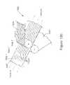
- the PV module 100is implemented in the configuration shown in FIG. 1A .
- the interconnecting regions 104can be shaped to reflect and concentrate reflected light onto PV regions 102 .
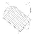
- FIGS. 2A and 2Billustrate a perspective view and a partial cross-sectional view of a PV module 200 having PV regions 202 and shaped interconnecting regions 204 .
- the percentage of the surface area of the PV regions 202 to the remaining surface area of the PV module 200is in a range between 20% to 80%, or less than 20% or greater than 80%.
- the shaped interconnecting regions 204are concentrators in some examples. As such, the shaped interconnecting regions 204 reflect and concentrate light onto PV regions 202 , reducing the amount of PV region 202 surface area needed to produce an equivalent amount of power.
- the PV module 200includes shaped concentrator regions 204 , the PV module 200 is otherwise substantially similar to the PV module 100 of FIGS. 1A-1D .
- the PV module 200includes longitudinally continuous edge caps 206 .
- the PV module 200includes a top layer 208 , active layer 210 , and bottom layer 212 .
- the top layer 208includes a substantially transparent film 214 , a plurality of top layer conductive strips 216 , and a top adhesive layer 218 .
- a power collection grid 220is formed in the bottom surface of substantially transparent film 214 .
- the active layer 210includes a plurality of PV strips 222 that are longitudinally continuous and substantially flexible in some embodiments.
- the PV strips 222include thin-film PV materials.
- An isolation strip 224is disposed along a longitudinal edge of each PV strip 222 in some examples.
- the bottom layer 212includes a conductive backsheet 226 and a plurality of bottom layer conductive strips 228 .
- a first bottom adhesive layer 230secures the bottom layer conductive strips 228 to the conductive backsheet 226 .
- each of bottom layer conductive strips 228includes one or more electrical contact strips 232 .
- a second bottom adhesive layer 234secures the top layer 208 , active layer 210 and bottom layer 212 together.
- the PV modules 100 , 200include a constrained layer damper to provide passive vibration damping introduced by wind or other environmental effects.
- a constrained layer damperincludes two metal materials sandwiching a visco-elastic material.
- the PV modules 100 , 200include top layer conductive strips 116 , 216 and bottom layer conductive strips 136 , 228 that are made of metal, where the top layer conductive strips 116 , 216 and bottom layer conductive strips 136 , 228 sandwich second bottom adhesive layer 146 , 234 made of a visco-elastic material.
- the top layer conductive strips 116 , 216 , bottom layer conductive strips 136 , 228 and second bottom adhesive layer 146 , 234form a constrainer layer damper.
- the constrained layer damperis effective at absorbing sound induced vibrations in the frequency range of 50 Hz to 10 kHz, or even less than 50 Hz or more than 10 kHz.
- FIGS. 3A-3Ban example top layer 300 is disclosed that may correspond to one or both of the top layers 108 , 208 of FIGS. 1A-2B .
- FIG. 3Ais a perspective view of the top layer 300 including a plurality of power collection regions 302 A, 302 B (collectively “power collection regions 302 ”) and a plurality of interconnecting regions 304 .
- FIG. 3Bis a cross-sectional view of a portion of the top layer 300 .
- the top layer 300is shown with only two power collection regions 302 and two interconnecting regions 304 , in other embodiments the top layer 300 includes more or less than two power collection regions 302 and two interconnecting regions 304 .
- the top layer 300includes a substantially transparent film 306 and a plurality of top layer conductive strips 307 (only one top layer conductive strip 307 is shown in FIG. 3B ).
- the substantially transparent film 306is approximately 15-300 microns thick in some examples.
- the substantially transparent film 306includes a weatherability film 308 , a first top adhesive layer 310 , a barrier layer film 312 , and a second top adhesive layer 314 .
- the weatherability film 308is configured to provide ultraviolet (“UV”) protection to a corresponding active layer and/or to be substantially resistant to hydrolysis such that exposure to moisture does not substantially break down the weatherability film 308 .
- the weatherability film 308includes fluorinated material(s) such as polytetrafluoroethylene (“PTFE”), poly methyl methacrylate (“PMMA”), or the like or any combination thereof.
- the first top adhesive layer 310is configured to secure the weatherability film 308 and the barrier layer film 312 together.
- the barrier layer film 312is configured to be substantially impenetrable to water and moisture.
- the second top adhesive layer 314is configured to secure the top layer conductive strips 307 to the top layer 300 .
- one or both of the first and second top adhesive layers 310 , 314includes ethylene-vinyl acetate (“EVA”) or other suitable adhesive(s) and is 5 to 100 microns thick, or even less than 5 microns or more than 100 microns thick.
- EVAethylene-vinyl acetate
- the top layer 300has been discussed as including a substantially transparent film 306 made up of a weatherability film 308 and barrier layer film 312 .
- the weatherability film 308 and barrier layer film 312can be implemented in separate films rather than in the substantially transparent film 306 .
- the power collection regions 302 A, 302 Bcollectively include a power collection macro grid 316 intermittently formed on a bottom surface of the top layer 300 .
- the power collection macro grid 316corresponds to the power collection grid 120 , 220 of FIGS. 1A-2B in some examples.
- the formation of the power collection macro grid 316is intermittent insofar as the power collection macro grid 316 is only formed in power collection regions 302 , rather than throughout the top layer 300 .
- the power collection macro grid 316is configured to collect power generated by corresponding PV strips positioned beneath the power collection regions 302 .
- the power collection macro grid 316 within each power collection region 302includes one or more interconnected grid lines 318 , 320 , 322 configured to contact the TCO of a corresponding PV strip and the top of an adjacent top layer conductive strip 307 so as to collect the power off the top of the PV strip and send it to the adjacent top layer conductive strip 307 .
- the power collection macro grid 306is intermittently formed on the bottom surface of the top layer 300 in some examples.
- the power collection macro grid 316is one example of a structural implementation of a means for collecting power from a plurality of PV strips.
- the power collection macro grid 316 within each power collection 302includes one or more interconnected grid lines 318 , 320 , 322 .
- One example of a grid pattern of interconnected grid lines of power collection macro grid 316is shown in the power collection regions 302 of FIG. 3A , although other grid patterns can alternately or additionally be implemented.
- the interconnected grid lines 318 , 320 , 322are 50 to 200 microns wide in the x-direction and 50 to 200 microns deep in the z-direction.
- the power collection macro grid 316can be formed using any method(s) and/or material(s) now known or later developed.
- the power collection macro grid 316is formed by partially perforating a bottom surface 324 of the top layer 300 A through the substantially transparent film 306 to form a desired grid pattern.
- the penetration depth of the perforations into the substantially transparent film 306is in a range of 30% to 50% of the thickness of the substantially transparent film 306 , or even less than 30% or more than 50% in some embodiments.
- the partial perforationscan be formed using a laser, for example.
- a screen printing or other techniquecan be used to fill the perforated areas with a conductive material that is in a paste or other spreadable form.
- the conductive materialis cured to drive off organic materials from the conductive material.
- the screen printing or other techniquesuch as stenciling, is tailored to form protruding profiles on bottom surfaces of the interconnected grid lines 318 , 320 , 322 .
- Such protruding profilesare configured to ensure contact of the interconnected grid lines 318 , 320 , 322 with a TCO of an underlying PV strip while substantially preventing the interconnected grid lines 318 , 320 , 322 from shorting to the substrate of the underlying PV strip.
- PV strips made from thin-film PV materialcan include many defects and/or inclusions.
- the amount of contact area between the interconnected grid lines 318 , 320 , 322 and TCO of the underlying PV stripis smaller than if the bottom surfaces of interconnected grid lines 318 , 320 , 322 were substantially planar, such that the likelihood of the interconnected grid lines 318 , 320 , 322 contacting a defect/inclusion and shorting to the substrate of the PV strip is reduced.
- the shape and dimensions of the interconnected grid lines 318 , 320 , 322allow for gridline failure in the event of a short circuit to the substrate of the PV strip. Accordingly, in some examples, in the event of a short circuit to the substrate of an underlying PV strip, a large current will flow into the affected interconnected grid line 318 , 320 , 322 in the area of the short circuit. Accordingly, the interconnected grid lines 318 , 320 , 322 are configured to open up in the region of the short circuit from the large current flow so as to isolate the short circuit.
- FIGS. 4A-4Banother example top layer 400 is disclosed that may correspond to one or both of the top layers 108 , 208 of FIGS. 1A-2B .
- FIG. 4is a perspective view of the top layer 400 including a plurality of power collection regions 402 and a plurality of interconnecting regions 404 .
- FIG. 4Bis a cross-sectional view of a portion of the top layer 400 .
- FIG. 4Cis a top view of a portion of a power collection region 402 .
- the top layer 400is shown with only two power collection regions 402 and two interconnecting regions 404 , in other embodiments the top layer 400 includes more or less than two power collection regions 402 and two interconnecting regions 404 .
- top layer 400 of FIGS. 4A-4Cis similar in some respects to the top layer 300 of FIGS. 3A-3B .
- top layer 400includes a substantially transparent film 406 and a plurality of top layer conductive strips 407 (only one top layer conductive strip 407 is shown in FIG. 4B ).
- Substantially transparent film 406includes a weatherability film 408 , a first top adhesive layer 410 , a barrier layer film 412 , and a second top adhesive layer 414 .
- the power collection regions 402collectively include a power collection nano grid 416 intermittently formed on a bottom surface of top layer 400 .
- the power collection nano grid 416corresponds to the power collection grid 120 , 220 of FIGS. 1A-2B in some examples.
- the power collection nano grid 416is similar in function to the power collection macro grid 316 of FIGS. 3A-3B . Namely, the power collection nano grid 416 is configured to collect power generated by corresponding PV strips positioned beneath the power collection regions 402 .
- the power collection nano grid 416 within each power collection region 402includes a plurality of conductive nano particles arranged in an interconnected network 418 of conductive traces 420 .
- FIG. 4Cillustrates one example of such an interconnected network 418 of conductive traces 420 .
- the power collection nano grid 416can be formed using any method(s) and/or material(s) now known or later developed.
- the power collection nano grid 416is formed by using a thin emulsion or other technique to apply an emulsion including nano-scale conductive particles to the bottom surface of top layer 400 .
- the emulsionis then annealed at an appropriate temperature to form the interconnected network 418 of conductive traces 420 .
- the nano-scale conductive particlescan include silver and/or other conductive metal(s) that self-assemble into the interconnected network 418 .
- the power collection nano grid 416is 80% to 95% transparent to light.
- the power collection nano grid 416is formed on the entire bottom surface of top layer 400 , followed by ablating the power collection nano grid 416 from the interconnecting regions 404 so that the power collection nano grid 416 is confined to the power collection regions 402 .
- the power collection nano grid 416is formed only in the power collection regions 402 by applying the emulsion to the power collection regions 402 using a spatially controlled process.
- the conductive traces 420are disposed in the second top adhesive layer 414 .
- the second top adhesive layer 414can be applied to the top layer 400 prior to formation of the power collection nano grid 416 and/or in such a way that the second top adhesive layer 414 is contained in regions between the individual conductive traces 420 to allow the conductive traces 420 to contact the TCO of the underlying PV strips.
- FIGS. 3A-3Billustrate a top layer 300 including a power collection micro grid 316 and FIGS. 4A-4C illustrate a top layer 400 including a power collection nano grid 416 .
- Embodiments disclosed hereininclude top layers having either a power collection micro grid or a power collection nano grid as well as top layers having both a power collection micro grid and a power collection nano grid. In some embodiments including both a power collection macro grid and a power collection nano grid, the power collection nano grid is applied to the top layer after formation of the power collection micro grid.
- each top layer 300 , 400includes a plurality of top layer conductive strips 307 , 407 .
- each of the top layer conductive strips 307 , 407includes rolled or extruded metal, laminated metal and plastic, or the like or any combination thereof.
- the metal used in top layer conductive strips 307 , 407may include one or more of aluminum, stainless steel, copper, tin, nickel, aluminum, copper, tin, silver, non-stainless steel low carbon steel, or the like or any combination thereof.
- each of the top layer conductive strips 307 , 407includes a coating of nickel, aluminum, copper, tin, silver, or strained layers of polyethylene terephthalate.
- the conductivity of the top layer conductive strips 307 , 407is in the range of 10 ⁇ 6 ohm-meters to 10 ⁇ 8 ohm-meters.
- top layer conductive strips 307 , 407are approximately 0.5 to 10 milli-inches (“mils”) thick (e.g., in the z-direction) and/or are plastically deformable.
- top layer conductive strips 307 , 407are formed by rolling, casting, depositing, or other suitable method(s).
- top layers 300 , 400include an overlap along one edge of top layer conductive strips 307 , 407 with the power collection macro or nano grids 316 , 416 as shown in FIGS. 3B and 4B .
- the overlapis approximately 0.5 to 1 millimeter (“mm”) in some examples.
- the top layer conductive strips 307 , 407are configured to electrically contact the power collection macro or nano grids 316 , 416 .
- the top layer conductive strips 307 , 407make electrical contact with the power collection macro or nano grids 316 , 416 in the area of overlap using mechanical contact, welding, ultrasonic bonding, pre-solder reflow, indium solder, conductive tape, or the like or any combination thereof.
- FIG. 5illustrates a partial cross-section of a PV module 500 lacking a power collection grid.
- the PV module 500is similar in some respects to the PV modules 100 and 200 of FIGS. 1A-2B and includes a top layer 502 , an active layer 504 and a bottom layer 506 .
- the top layer 502includes a substantially transparent film 508 and a plurality of top layer conductive strips 510 .
- the active layer 504includes a plurality of PV strips 512 .
- the bottom layer 506includes a conductive backsheet 514 and a plurality of bottom layer conductive strips 516 .
- Contact strips 518are disposed on the bottom layer conductive strips 516 to connect adjacent pairs of top layer conductive strips 510 and PV strips 512 .
- the PV module 500lacks a power collection grid disposed above the PV strips 512 for collecting power from the TCO of each PV strip 512 and connecting the TCO of each PV strip 512 to an adjacent top layer conductive strip 510 .
- each top layer conductive strip 510extends over the top of an adjacent PV strip 512 and contacts the TCO of the adjacent PV strip 512 through contact strips 520 .
- the top layer conductive strips 510are another example of a structural implementation of a means for collecting power from a plurality of PV strips 512 .
- the active layer of PV modulesis prepared from a continuous sheet of thin-film PV material.
- Such continuous sheets of thin-film PV materialcan be formed in virtually any desired dimensions and/or on flexible substrates suitable for roll-to-roll processing of the type described below.
- FIG. 6illustrates an example processing flow for preparing the active layer 110 of PV module 100 .
- a continuous sheet 600 of thin-film PV material(“PV sheet 600 ”) is formed.
- the term “continuous” as applied to the PV sheet 600means that the PV sheet 600 is substantially continuous in the arbitrarily-defined x-y plane over the dimensions of the PV sheet 600 in the x- and y-directions, as opposed to being divided into discrete solar cells.
- the PV sheet 600has finite dimensions in the x- and y-directions and the PV sheet 600 is substantially continuous along the entirety of the finite dimensions in the x- and y-dimensions.
- the PV sheet 600includes substrate 124 , thin-film active layer 126 and TCO 128 , discussed above with respect to FIGS. 1A-1D .
- TCO-free regions 130are formed by ablating the TCO 128 from the PV sheet 600 in the regions 130 .
- the width in the x-direction of each region 130is approximately 100 microns to 400 microns. Alternately, the width of each region 130 is less than 100 microns or more than 400 microns.
- the TCO 128is ablated from regions 130 by directing a laser at the regions 130 .
- the laser used to ablate TCO 128 from regions 130can include, for instance, a quadrupled Nd:YAG laser, a quadrupled Nd:YLF laser, a fiber pumped laser, a solid state laser, an excimer laser, a gas laser, or the like or any combination thereof.
- the laseris configured to emit light in the near-ultraviolet (“near-UV”) wavelength range, e.g., 400 nanometers (“nm”) to 300 nm.
- the laseris configured to emit light in the UV wavelength range, e.g., 400 nm to 10 nm.
- regions 130 during stage 2isolates the PV sheet 600 into PV regions 602 that are ultimately separated from each other to form PV strips 122 in stage 3 .
- PV strips 122are formed by cutting through regions 130 .
- the cutsare abstractly represented by lines 604 in stage 3 .
- the cuts 604are made substantially in the middle of regions 130 .
- the regions 130are formed and the cuts 604 are made such that a width 606 of each PV strip 122 is in the range of 25 mm to 200 mm.
- the width 606 of PV strips 122is substantially the same from one PV strip 122 to another.
- the width 606 of PV strips 122is variable from one PV strip 122 to another.
- the PV strips 122are formed by directing a laser at the regions 130 along the cutting lines 604 .
- the laser used to cut through regions 130can include, for instance, an Nd:YAG laser, an Nd:YLF laser, a fiber pumped laser, a carbon dioxide laser, an excimer laser, a solid state laser, a gas laser, or the like or any combination thereof.
- the laseris configured to emit light in the near-infrared (“near-IR”) wavelength range, e.g., 750 nm to 1400 nm, and/or up to a wavelength of 10 microns or beyond.
- near-IRnear-infrared
- the PV strips 122can be formed using a mechanical cutter, rather than a laser cutter.
- the PV strips 122are separated, using, for instance, an inline separator (not shown).
- the PV strips 122are separated to include 200 microns to 500 microns of spacing in some embodiments.
- a dispensing system 608applies a protection layer 610 to the exposed regions 130 to protect the thin-film active layer 126 and/or substrate 124 against moisture ingress, chemical attack and/or ionic contamination.
- the protection layer 610includes dielectric, sealant, desiccant, a silicone-based product, or the like or any combination thereof.
- the separated PV strips 122are laminated to a top layer and/or bottom layer as explained in greater detail below.
- the bottom layer 112 , 212 of PV module 100 , 200includes bottom layer conductive strips 136 , 228 .
- each of the bottom layer conductive strips 136 , 228includes rolled or extruded metal, laminated metal and plastic, or the like or any combination thereof.
- the bottom layer conductive strips 136 , 228are approximately 0.5 to 10 mils thick (e.g., in the z-direction).
- the bottom layer 112 , 212 of PV module 100 , 200is prepared by laminating the bottom layer conductive strips 136 , 228 over the first bottom adhesive layer 138 , 230 onto conductive backsheet 134 , 226 .
- the conductive backsheet 134 , 226is a conductive and environmentally protective film in some embodiments.
- the conductive backsheet 134 , 226can include aluminum with or without a polyethylene terephthalate (“PET”) film or other suitable material(s) on its bottom surface.
- the bottom layers 112 , 212include an insulating layer between the conductive backsheet 134 , 226 and the bottom layer conductive strips 136 , 230 , which insulating layer is made of PET or PMMA in some examples.
- the insulating layeris a PET layer with separate EVA sheets of adhesive for attachment, or a PET layer with co-extruded faces of EVA on the PET layer, or some combination thereof.
- the conductive backsheet 134 , 226is an extruded, cast, rolled, or other type of metal film attached to the insulating layer.
- the exposed (e.g., bottom) surface of the conductive backsheet 134 , 226is black and/or has an emissivity greater than 0.6, allowing for improved thermal emissions to aid in PV module 100 , 200 cooling.
- the bottom layer conductive strips 136 , 228cooperate with the top layer conductive strips 116 , 216 and power collection grid 120 , 220 to serially and redundantly interconnect the PV strips 122 , 222 together.
- bottom layer conductive stripscan be configured to serially and redundantly interconnect PV strips together without top layer conductive strips and/or power collection grids.
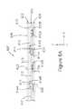
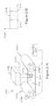
- FIG. 7Adiscloses a cross-sectional view of an example PV module 700 having double overlap bottom layer conductive strips such that top layer conductive strips and/or a power collection grid are not implemented in the PV module 700 .
- the PV module 700includes a top layer 702 , active layer 704 and bottom layer 706 .
- the top layer 702includes a substantially transparent film 708 and a plurality of gimbal strips 710 .
- the active layer 704includes a plurality of PV strips 712 .
- the bottom layer 706includes a plurality of bottom layer conductive strips 714 and a conductive backsheet 715 .
- each gimbal strip 710includes two contact strips 710 A, 710 B disposed on a bottom surface of the gimbal strip 710 .
- each bottom layer conductive strip 714includes one or more contact strips 714 A, 714 B disposed on the right side of each bottom layer conductive strip 714 beneath a corresponding PV strip 712 .
- the contact strips 710 A, 710 B, 714 A, 714 Binclude a relatively soft, electrically conductive material that is rounded in some embodiments.
- the left contact strip 710 A of each gimbal strip 710contacts the TCO of the PV strip 712 immediately to the left of the gimbal strip 710 , electrically connecting the TCO of the PV strip 712 to the gimbal strip 710 .
- the right contact strip 710 Bcontacts a top surface of the bottom layer conductive strip 714 immediately to the right of the gimbal strip 710 such that the TCO of each PV strip 712 is electrically connected to the bottom layer conductive strip 714 immediately to the right of the PV strip 712 .
- each bottom layer conductive strip 714contact the substrate of the PV strip 712 immediately to the right of the bottom layer conductive strip 714 such that the substrate of each PV strip 712 is electrically connected to the bottom layer conductive strip 714 immediately to the left of the PV strip 712 .
- the bottom layer conductive strips 714 and gimbal strips 710serially and redundantly interconnect the PV strips 712 without any top layer conductive strips.
- gimbal strips 710are made from a continuous sheet of gimbal material that is optionally in a roll form.
- the continuous sheet of gimbal materialis slit, separated, and laminated to the top layer 702 at appropriate locations to interconnect the TCO of each PV strip 712 to the bottom layer conductive strip 714 immediately to the right of the PV strip 712 .
- adhesives, epoxies, tapes, or other materialsare used to ensure that contact strips 710 A, 710 B of gimbal strip 710 are securely connected to the TCO of the corresponding PV strip 712 or the top surface of the corresponding bottom layer conductive strip, respectively.
- the slicing of the continuous sheet of gimbal material and/or the addition of the contact strips 710 A, 710 Bcan be performed using any method(s) and/or material(s) now known or later developed. Examples of such methods and/or materials include laser cutting, ball bonding, cladding, brazing, soldering, conductive epoxy dispense, vias and interconnects in flexible electronic circuits, or the like or any combination thereof.
- each bottom layer conductive strip 714partially overlaps the two PV strips 712 to the left and right of the bottom layer conductive strip 714 in the areas of overlap 716 A, 716 B.
- a substantially electrically isolating materialis disposed between the bottom layer conductive strips 714 and PV strips 712 at least in the areas of overlap 716 A, 716 B so as to electrically isolate the PV strips 712 from the bottom layer conductive strips 714 except where a connection is desired, e.g., along the contact strips 714 A, 714 B of bottom layer conductive strips 714 .
- the electrically isolating materialincludes a substantially electrically isolating adhesive or other suitable material(s).
- a substantially electrically isolating materialis disposed between the bottom layer conductive strips 714 and PV strips 712 in the areas of overlap 716 B, while a substantially electrically conducting material is disposed between the bottom layer conductive strips 714 and PV strips 712 in the areas of overlap 716 A.
- the substantially electrically conducting material disposed in the areas of overlap 716 Aincludes conductive adhesive, conductive epoxy, conductive tape, or the like, and can be used alone or in combination with contact strips 714 A, 714 B
- the PV module 700is illustrated in a shaped configuration.
- the bottom layer conductive strips 714have been formed to create concentrators 718 .
- the module 700includes a power collection grid formed in the top layer 702 above the PV strips 712 .
- the power collection gridmay be a power collection macro grid, a power collection nano grid, or any combination thereof. Alternately, the module 700 can be implemented without a power collection grid.
- FIG. 8Adiscloses another example of a PV module 800 having double overlap bottom layer conductive strips such that top layer conductive strips and/or a power collection grid are not implemented in the PV module 800 .
- the PV module 800is similar in some respects to the PV module 700 of FIG. 7A .
- the PV module 800includes a top layer 802 , active layer 804 and bottom layer 806 .
- the top layer 802includes a substantially transparent film 808 .
- the active layer 804includes a plurality of PV strips 810 .
- the bottom layer 806includes a plurality of bottom layer conductive strips 812 and a conductive backsheet 814 .
- each bottom layer conductive strip 812includes one or more contact strips 812 A, 812 B disposed on the right side of each bottom layer conductive strip 812 beneath a corresponding PV strip 810 .
- the contact strips 812 A, 812 B of each bottom layer conductive strip 812contact the substrate of the PV strip 810 immediately to the right of the bottom layer conductive strip 812 such that the substrate of each PV strip 810 is electrically connected to the bottom layer conductive strip 812 immediately to the left of the PV strip 810 .
- the PV module 800 of FIG. 8Aincludes a plurality of stitched contact strips 814 , rather than a plurality of gimbal strips 710 .
- the stitched contact strips 814include a plurality of contact points 814 A, 814 B.
- the left contact points 814 A of each stitched contact strip 814contact the TCO of the PV strip 810 immediately to the left of the stitched contact strip 814 , electrically connecting the TCO of the PV strip 712 to the stitched contact strip 814 .
- each stitched contact strip 814contact a top surface of the bottom layer conductive strip 812 immediately to the right of the stitched contact strip 814 such that the TCO of each PV strip 810 is electrically connected to the bottom layer conductive strip 812 immediately to the right of the PV strip 810 .
- the substrate of each PV strip 810is electrically connected to the bottom layer conductive strip 812 immediately to the left of the PV strip 810 .
- the stitched contact strips 814 and bottom layer conductive strips 812serially and redundantly interconnect the PV strips 810 together without any top layer conductive strips.
- the stitched contact strips 814are made by stitching a wire into the top layer 802 .
- the wire usedis approximately 12 to 75 microns in diameter in some embodiments.
- the wireincludes copper, gold, aluminum, gold-coated tin wire, or other suitable material(s).
- the wireincludes an insulating outer layer.
- Each stitched contact strip 814is stitched in an appropriate location of the top layer 802 so as to interconnect the TCO of each PV strip 810 to the bottom layer conductive strip 812 immediately to the right of the PV strip 810 .
- FIG. 8Billustrates several example stitch patterns 816 , 818 for stitched contact strips 814 that can be implemented in the top layer 802 according to some embodiments.
- every stitched contact strip 814 of PV module 800implements the same stitch pattern 816 or 818 , while in other embodiments multiple stitch patterns 816 , 818 are implemented within the same PV module.
- FIG. 8Bfurther includes reference lines 820 , 822 , 824 , all three of which are also depicted in FIG. 8A .
- Reference lines 820 and 824correspond to separations in the x-direction of the PV strips 810 from the bottom layer conductive strips 812 .
- Reference line 822corresponds to the leftmost side of one of the PV strips 810 .
- the stitched contact strips 814are stitched into the top layer 802 so as to span the separation in the x-direction between the PV strips 810 and the bottom layer conductive strips 812 . Accordingly, when the top layer 802 , active layer 804 and bottom layer 806 are laminated together, the stitched contact strips 814 are positioned in the top layer 802 so that left contact points 814 A contact the TCO of corresponding PV strip 810 and right contact points 814 B contact the top surface of the corresponding bottom layer conductive strip 812 .
- Both of stitch patterns 816 , 818include a pitch 826 , where pitch 826 is defined as the distance in the y-direction from one left or right contact point 814 A, 814 B to the next left or right contact point 814 A, 814 B.
- the pitch 826can be substantially constant, as in the stitch patterns 816 , 818 , or variable (not shown). In some examples, the pitch 826 is between 0.5 mm and 3 mm.
- Both of stitch patterns 816 , 818also include a first lateral incursion and/or a second lateral incursion.
- the first lateral incursionis defined as the distance in the x-direction from the rightmost edge (generally corresponding to reference lines 820 , 824 ) of an underlying PV strip 810 to left contact points 814 A
- the second lateral incursionis defined as the distance in the x-direction from the rightmost edge of an underlying PV strip 810 to right contact points 814 B.
- the first and/or second lateral incursionsmay be constant or variable.
- the stitch pattern 816includes constant first and second lateral incursions
- the stitch pattern 818includes a variable first later incursion and a constant second lateral incursion.
- the stitch pattern 818variably encroaches over the underlying PV strip 810 along the length of the stitched contact strip 814 having stitch pattern 818 .
- stitch pattern 818functions as a power collection grid, despite being different in implementation from the power collection macro and nano grids described above with respect to FIGS. 3A-4C .
- the variable first lateral incursion of stitch pattern 818permits the stitched contact strip 814 with stitch pattern 818 to collect power from the TCO of an underlying PV strip 810 at multiple locations across the width of the underlying PV strip 810 , for reduced parasitic capacitance in the underlying PV strip 810 .
- a ball or other enlarged portion of conductive materialis formed at each contact point 814 A, 814 B to ensure good contact with the TCO of the corresponding PV strip 812 or the top surface of the corresponding bottom layer conductive strip.
- the ball or other enlarged portioncan be formed in stitched contact strips 814 during or after the stitching of the stitched contact strips 814 into the top layer 802 .
- the insulationis stripped at least from the contact points 814 A, 814 B during or after the stitching of the stitched contact strips 814 into the top layer 802 .
- the insulationis left on the stitched contact strips 814 substantially everywhere except at the contact points 814 A, 814 B so as to prevent the stitched contact strips 814 from shorting to the substrate of the PV strips 810 where the stitched contact strips 814 cross over the edges of the PV strips 810 .
- the stitched contact strips 814are made from wire that is at least partially reflective of light.
- the stitched contact strips 814can be made from wire that is polished or extruded to be at least partially reflective or from wire that includes a coating that is at least partially reflective of light.
- the stitched contact strips 814may be configured to reflect light onto PV strips 810 .
- the diameter, conductivity, and/or electromigration properties of the stitched contact strips 814are selected to ensure designed failure in the event of a shunting defect occurring at or in proximity of the stitched contact strip 814 contact location to the TCO of the underlying PV strip 810 .
- Such designed failurein some examples minimizes functional and reliability impact of shunting defects and is described in greater detail in U.S. Provisional Application Ser. No. 61/022,240, filed Jan. 18, 2008 and entitled INTEGRATED DEFECT MANAGEMENT FOR A THIN-FILM PHOTOVOLTAIC SYSTEM.
- FIG. 9illustrates a block diagram of an example electronic circuit layer 900 and power conversion circuits 902 that may correspond to the electronic circuit layer 142 and power conversion circuits 144 of FIGS. 1A-1D .
- the electronic circuit layer 900is a flexible circuit. As shown in FIG. 9 , the electronic circuit layer 900 includes an input bus 904 , current return bus 906 and conditioned output bus 908 . Alternately or additionally, the electronic circuit layer further includes one or more digital control lines 910 , 912 .
- the input bus 904is configured to be connected to the last PV strip of a PV module in which the electronic circuit layer 900 is implemented.
- the input bus 904in some embodiments is connected to the last PV strip 122 D, e.g., through first vias 142 A and/or power collection grid 120 C, of PV module 100 of FIG. 1D .
- the input bus 904is further configured to be connected to inputs of the power conversion circuits 902 . Accordingly, the input bus 904 collects current from the series-connected PV strips of the PV module and distributes the current to the power conversion circuits 902 .
- the current return bus 906is configured to be connected to the conductive backsheet of a PV module in which the electronic circuit layer 900 is implemented.
- the current return bus 906in some embodiments is connected to the conductive backsheet 134 , e.g., through second vias 142 B and/or contact strip 140 F, of the PV module 100 of FIG. 1D .
- the current return bus 906is further configured to be connected to current return outputs of power conversion circuits 902 . Accordingly, the current return bus 906 is part of the current return path for the series-connected PV strips of the PV module in which the electronic circuit layer 900 is implemented.
- the conditioned output bus 908is configured to be connected to the conditioned outputs of power conversion circuits 902 .
- the conditioned output bus 908collects the conditioned power generated by power conversion circuits 902 and carries the conditioned power to the end(s), e.g., the positive and/or negative y side, of the electronic circuit layer 900 and PV module.
- the digital control lines 910 , 912are differential digital control lines. In other embodiments, the digital control lines 910 , 912 are implemented as a single-ended digital control line.
- the digital control lines 910 , 912can be used by a control module, e.g., processor, controller, microprocessor, microcontroller, or the like, to control operation of the power conversion circuits 902 .
- a control modulee.g., processor, controller, microprocessor, microcontroller, or the like
- One or more of the power conversion circuits 902may include a control module and/or a discrete control module may be provided for the purpose of controlling the power conversion circuits 902 via digital control lines 910 , 912 .
- the power generated by the PV moduleis collected on the input bus 904 and distributed to power conversion circuits 902 , where the power conversion circuits 902 output conditioned power on the conditioned output bus 908 and return current through the current return bus 906 and conductive backsheet.
- the power conversion circuits 902are configured to generate conditioned power by converting a first voltage collectively generated by the PV strips of a PV module to a second voltage that is larger than the first voltage.
- the resulting conditioned power output of the power conversion circuits 902therefore has a relatively lower current than the power generated by the PV strips, making it more suitable for transmission to a battery and/or a load without the need for large transmission wires or cables.
- the power conversion circuits 902collectively convert 200 watts of direct current (“DC”) electrical power at 8 volts and 25 amps to 200 watts DC at 48 volts and 4.2 amps.
- DCdirect current
- the power conversion circuits 902may collectively convert 200 watts DC at 8 volts and 25 amps to 200 watts DC at 35-60 volts and 5.7-3.3 amps.
- the specific voltage and amperage values for the input and conditioned power output discussed hereinare provided by way of example only and should not be construed to limit the invention.
- one or more of the power conversion circuits 902are redundant, such that not all of the power conversion circuits 902 are required during operation.
- the current capacity of each of power conversion circuits 902is at least 2 times a normal operating current.
- the power conversion circuits 902are balanced using one or more of pulse-width modulated (“PWM”) control, phasing of each power conversion circuit 902 relative to other power conversion circuits 902 and defect management.
- PWMpulse-width modulated
- the PV strips 102collectively generate a voltage of 2 to 20 volts and a current that varies with illumination intensity, but that may be anywhere between 10-60 amps per lineal foot of PV module 100 in the y direction.
- the power conversion circuits 144are configured to step up the voltage and step down the current to make the power supply more suitable for long-distance transmission.
- the conductive backsheet 134can include metal that is an exposed or minimally insulated electrical ground, rather than being heavily insulated. In contrast, conventional PV modules can generate voltages up to 600 volts, requiring an enclosed current return path.
- the ability to implement an exposed or minimally insulated conductive backsheet 134 in PV module 100allows the conductive backsheet 134 to spread and dissipate thermal energy outside the PV module 100 more efficiently than PV modules that have insulated current return paths, thereby providing a relative improvement in thermal performance for the PV module 100 compared to some PV modules.
- FIGS. 10A-10Cillustrate different configurations of power conversion circuits.
- FIG. 10Aillustrates a PV module 1000 A having power conversion circuits 1002 arranged along one edge of the PV module 1000 A.
- the power output from the PV module 1000 Ais designated at 1004 and the current return path is designated at 1006 .
- FIG. 10Billustrates a PV module 1000 B having power conversion circuits 1008 arranged along both edges of the PV module 1000 B.
- the power output from PV module 1000 Bis designated at 1010 A and 1010 B and two current return paths are designated 1012 A and 1012 B.
- FIG. 10Cillustrates a PV module 1000 C having power conversion circuits 1014 arranged along the center of PV module 1000 C.
- the power output from PV module 1000 Cis designated at 1016 and two current return paths are designated at 1018 A and 1018 B.
- FIG. 11Aillustrates a wall-mounted horizontal configuration for a PV module 1100 A including a plurality of concentrators 1102 (only one is shown in FIG. 11A ) and PV regions 1104 .
- the PV module 1100 Ais mounted to a wall 1106 or other framing structure including one or more shaped supports 1108 extending horizontally across the wall 1106 .
- the shaped supports 1108are complementary in shape to the concentrators 1102 and the PV module 1100 A is mounted to the wall 1106 such that the concentrators 1108 align with the shaped supports 1108 so as to also extend horizontally.
- a plurality of fasteners 1110are inserted through the concentrators 1102 into the shaped supports 1108 to secure the PV module 1100 A to the wall 1106 .
- the fasteners 1110include one or more of metal or plastic nails, plastic-coated nails, rubber-coated nails, nails with sealing heads, metal or insulating-coated screws, screws with sealing heads, clips, or the like or any combination thereof.
- the shaped supports 1108can be discrete or continuous along the length of the PV module 1100 A.
- the PV module 1100 Acan be mounted to a framing structure made up of components, such as studs, that are discrete along the length and/or width of the PV module 1100 A, that permit air to circulate along the back side of the PV module 1100 A for PV module 1100 A cooling and/or that facilitate easy installation, serviceability, cleaning, and/or other maintenance.
- adhesivecan be provided between the concentrators 1102 and shaped supports 1108 and/or between the PV module 1100 A and the wall 1106 or other framing structure so as to secure the PV module 1100 A to the wall 1106 or other framing structure.
- FIG. 11Billustrates another wall-mounted horizontal configuration for a PV module 1100 B that is similar to the wall-mounted horizontal configuration of FIG. 11A .
- the PV module 1100 Bincludes a plurality of concentrators 1112 (only one is shown in FIG. 11B ) and PV regions 1114 .
- the PV module 1100 Bis mounted to a wall 1116 or other framing structure including one or more shaped supports 1118 extending horizontally across the wall 1116 .
- the PV module 1100 Bincludes a plurality of slots 1120 formed in the concentrators 1112 .
- the slots 1120are configured to receive clips 1122 or other fasteners to secure the PV module 1100 B to the wall 1116 .
- the slots 1120are periodically spaced in the concentrators 1112 .
- unused clips 1122can be flattened, e.g., hammered, flush against the shaped support 1118 prior to or after installation of the PV module 1100 B.
- sealantis placed over each slot 1120 after installation.
- FIG. 11Cillustrates a wall-mounted vertical configuration for a PV module 1100 C including a plurality of concentrators 1124 and PV regions 1126 .
- the configuration of FIG. 11Cis vertical insofar as the PV module 1100 C is mounted such that concentrators 1124 and PV regions 1126 extend substantially vertically.
- the upper portion of FIG. 11Cincludes a front view of the PV module 1100 C while the lower portion of FIG. 11C shows a cross-sectional view through section A-A identified in the upper portion of FIG. 11C .
- the PV module 1100 Cis mounted to a framing structure 1128 including shaped supports 1130 extending vertically.
- a plurality of fasteners 1132are inserted through the concentrators 1124 into the shaped supports 1130 to secure the PV module 1100 C to the framing structure 1128 .
- FIG. 11Dillustrates a roof-mounted configuration for a PV module 1100 D including a plurality of concentrators 1134 and PV regions 1136 .
- the PV module 1100 Dis mounted to a framing structure 1138 on a sloped roof, the framing structure 1138 including one or more shaped supports 1140 extending up and down the sloped roof.
- the PV module 1100 Dis mounted to the framing structure 1138 such that the concentrators 1134 also extend up and down the sloped roof.
- a plurality of fasteners 1142are inserted through the concentrators 1124 into the shaped supports 1140 to secure the PV module 1100 D to the framing structure 1138 .
- FIG. 11Eillustrates another roof-mounted configuration for a PV module 1100 E including a plurality of concentrators 1144 and PV regions 1146 .
- the PV module 1100 Eis mounted directly to a sloped roof 1148 by applying adhesive 1150 between substantially planar regions (e.g., PV regions 1146 ) of the PV module 1100 E and the sloped roof 1148 .
- Areas under the concentrators 1144are left open for air to circulate and provide passive cooling for the PV module 1100 E.
- heat generated in the PV regions 1146 during normal operationis at least partially transferred to the concentrators 1144 via thermal conduction and then transferred away from the concentrators 1144 by the air circulating beneath the concentrators 1144 .
- FIG. 11Fillustrates yet another roof-mounted configuration for a PV module 1100 D including a plurality of concentrators 1152 and PV regions 1154 .
- the PV module 1100 Fis mounted to a framing structure 1156 on a sloped roof, the framing structure 1156 including one or more shaped supports 1158 extending horizontally.
- the PV module 1100 Fis mounted to the framing structure 1100 F such that the concentrators 1152 also extend horizontally.
- a plurality of fasteners 1160are inserted through the concentrators 1152 into the shaped supports 1158 to secure the PV module 1100 F to the framing structure 1156 .
- FIG. 12Aan example PV module 1200 having PV regions 1202 and interconnecting regions 1204 is shown in which a plurality of fastener regions 1206 are formed in the interconnecting regions 1204 for receiving fasteners. As shown, the fastener regions 1206 are formed at regular intervals along the length of each interconnecting region. Alternately or additionally, the fastener regions 1206 are visible to the naked eye.
- FIG. 12Billustrates a cross-sectional view through a fastener region 1206 of the PV module 1200 .
- the PV module 1200further includes a substantially transparent film 1208 , a plurality of PV strips 1210 in the PV regions 1202 , a plurality of bottom layer conductive strips 1212 (only one is shown) in the interconnecting regions 1204 , a conductive backsheet 1214 , and various adhesive layers 1216 A, 1216 B, 1216 C.
- the fastener regions 1206include one or more through holes 1218 A, 1218 B formed in one or more conductive layers of the PV module 1200 .
- the fastener region 1206 of FIG. 12Bincludes a through hole 1218 A formed in the bottom layer conductive strip 1212 and a through hole 1218 B formed in the conductive backsheet 1214 .
- through holescan be formed in top layer conductive strips to form fastener regions in PV modules that have top layer conductive strips.
- the through holes 1218 A, 1218 Bare aligned to each other in the z-direction.
- the through holes 1218 A, 1218 Bare filled with adhesive from one or more of the adjacent adhesive layers 1216 A, 1216 B, 1216 C or with other fillers.
- the adhesive or other fillersare electrically insulating.
- the size (e.g., the diameter) of the through holes 1218 A, 1218 Bis larger than the size (e.g., the diameter) of a corresponding fastener 1220 configured to be inserted through the fastening regions 1206 .
- the fastener 1220includes a substantially cylindrical shaft 1222 that is smaller in diameter than the diameter 1224 of through holes 1218 A, 1218 B.
- the difference in sizes of the through holes 1218 A, 1218 B and shaft 1222 of fastener 1220is configured to substantially reduce the likelihood of the shaft 1222 shorting to the bottom layer conductive strip 1212 or conductive backsheet 1214 .
- the fasteners 1220implemented according to some embodiments include a head 1226 with sealing gasket 1228 .
- a sealant 1230can be applied to the substantially transparent film 1208 in the fastener region 1206 .
- the PV module 1200can be secured to a structure by inserting fasteners 1220 through fastener regions 1206 .
- the fasteners 1220can be hammered through or otherwise inserted through fastener regions 1206 such that the shaft 1222 of each such fastener 1220 penetrates through substantially transparent film 1208 , adhesive layers 1216 A and 1216 B, the through hole 1218 A of bottom layer conductive strip, adhesive layer 1216 C, the through hole 1218 B of conductive backsheet 1214 , and into an underlying support structure.
- the through holes 1218 A, 1218 Bare formed in the bottom layer conductive strips 1212 and/or conductive backsheet 1214 using stamping, cutting, drilling, or other suitable method(s). Alternately or additionally, the bottom layer conductive strips 1212 are cut from a continuous sheet of material, and the through holes 1218 A can be formed in the continuous sheet of material prior to cutting into the bottom layer conductive strips 1212 .
- FIG. 13provides additional passive cooling details regarding a mounting configuration that may correspond to the PV module 1100 E and mounting configuration of FIG. 11E .
- FIG. 13discloses a PV module 1300 having a plurality of concentrators 1302 (only one is shown) and a plurality of PV regions (not shown).
- the PV module 1300is mounted to a sloped roof 1304 .
- a vented ridge cap 1306 and flashing 1308are provided in some embodiments to allow the ends of the concentrators 1302 to remain open while substantially preventing the ingress of water under the PV module 1300 .
- radiant energy from the sunis absorbed by the PV regions and is at least partially transferred via thermal conduction to the concentrators 1302 .
- Air under the concentrators 1302is heated by convection and circulates upwards towards the vented ridge cap 1306 , eventually forcing heated air out through the vented ridge cap 1306 as represented by the arrow 1310 , and drawing un-heated air under the concentrators 1302 near the flashing 1308 as represented by arrow 1312 .
- the heated air 1310can be collected and used by a heating and ventilation system to heat a house or other building to which the sloped roof 1304 belongs.
- some embodiments disclosed hereinprovide load support for installing and maintaining the PV modules 1100 A- 1100 F.
- a laddercan be leaned against the PV modules 1100 A- 1100 C so as to rest against and therefore load one or more of the concentrators 1102 , 1112 , 1124 .
- the shaped supports 1108 , 1118 , 1130 and concentrators 1102 , 1112 , 1124provide support for the load of the ladder.
- an individualcould attempt to walk on or otherwise put his/her weight on the concentrators 1134 , 1152 of PV modules 1100 D, 1100 F, which concentrators 1134 , 1152 are supported by shaped supports 1140 , 1158 .
- a plank or boardcould be laid across the concentrators 1134 , 1152 to support the individual's weight.
- a support device 1400can be implemented such as depicted in FIG. 14 .
- the support device 1400is illustrated in the configuration of FIG. 11D using the same reference numbers as FIG. 11D where similar components are indicated. It will be appreciated, however, that the support device 1400 can be implemented in any of the configurations of FIGS. 11A-11F and/or in other configurations.
- the support device 1400includes a plurality of cutouts 1402 .
- the cutouts 1402are complementary in shape and spacing to the concentrators 1144 so as to partially receive concentrators 1144 .
- the cutouts 1402in some examples only partially receive concentrators 1144 so that the bottom of support device 1400 remains a distance 1404 away from PV regions 1146 to thereby protect the PV regions 1146 from loading damage during installation and/or maintenance of PV module 1100 D.
- the cutouts 1402can be partially or completely coated with rubber or other protective coating to protect the concentrators 1144 from being damaged when a load is applied to the support device 1400 .
- the support device 1400can be permanently installed with the PV module 1100 D or temporarily implemented during installation and/or maintenance of the PV module 1100 D.
- FIGS. 15A-15Ca PV module 1500 is disclosed that includes a plurality of discrete straps 1502 to support cross-directional loads on the PV module 1500 .
- FIG. 15Aillustrates an perspective view of the PV module 1500
- FIG. 15Billustrates an upside-down cross-sectional view of the PV module 1500 across the width of the PV module 1500 and length of a strap 1502
- FIG. 15Cillustrate a cross-sectional view of the PV module 1500 across the width of the strap 1502 of FIG. 15B .
- the PV module 1500includes a plurality of edge caps 1504 A, 1504 B.
- an electronic circuit layer and/or power conversion circuitsare housed within edge cap 1504 B.
- the straps 1502are configured to secure the PV module 1500 to a framing structure.
- the strap 1502includes hooked ends 1506 that are configured to removably engage a framing structure to which the PV module 1500 is attached.
- the straps 1502can include one or more rib structures to stiffen the straps 1502 (and consequently the PV module) in the x-direction.
- the strap 1502includes two rib structures 1508 .
- each strap 1502can include more or less than two rib structures 1508 .
- the straps 1502are spaced at periodic or random intervals along the length of the PV module 1500 and, as previously indicated, can be used to secure the PV module 1500 to a framing structure. Alternately or additionally, the straps 1502 elevate the PV module 1500 above the framing structure. Accordingly, it will be appreciated, with the benefit of the present disclosure, that the spacing of the straps 1502 and/or the elevation of the PV module 1500 above the framing structure allow for air circulation along a corresponding conductive backsheet of the PV module 1500 for PV module 1500 cooling in some embodiments.
- embodiments of the inventioninclude PV modules having shaped interconnecting regions that are concentrators in some embodiments.
- the concentratorsare configured to reflect and concentrate light onto adjacent PV regions of the PV modules.
- the width (e.g., at the base of each concentrator), height, shape, spacing and/or various other aspects of the concentratorscan be varied according to a desired application and/or can be selected to optimize the output of the PV modules and may depend on one or more factors including an installation angle and/or installation latitude at an installation site.
- the concentrators disclosed hereinare similar to reflective louvers described in U.S. patent application Ser. No. 12/357,277, entitled “Detachable Louver System,” filed Jan.
- louversAlthough the application Ser. No. 12/357,277 discusses louvers, it will be appreciated that many or all of the principles applied to the louvers can be analogously applied to the concentrators disclosed herein.
- concentratorsare formed from corresponding interconnecting regions by stamping or other methods section-by-section along the length of the PV module. Alternately or additionally, concentrators are formed in roll-to-roll operations from a sheet of PV module material prior to cutting the sheet of PV module material into discrete PV modules. Alternately or additionally, the PV modules can be shipped flat or in rolls to an installation site, whereupon concentrators are formed at the installation site prior to installation.
- concentratorsprovide bending stiffness to PV modules in which the concentrators are implemented.
- the bending stiffness provided by the concentratorsis sufficient to permit PV modules to be supported by cross-direction support pieces (e.g., support pieces that are aligned substantially normal to the length of the concentrators) that are spaced on one foot to six foot centers and/or that support nominal live loadings such as ice, rain and snow roof loadings, wind loadings, and the like or any combination thereof.
- FIGS. 16A and 16Bvarious details regarding PV modules 1600 A and 1600 B having concentrators 1602 , 1604 and PV regions 1606 , 1608 disclosed.
- FIG. 16Adepicts the PV module 1600 A in a static horizontal orientation
- FIG. 16Bdepicts the PV module 1600 B in a static vertical orientation.
- the concentrators 1602 , 1604are aligned to the sun's relative motion through the sky. That is, the concentrators 1602 , 1604 may generally be aligned east to west.
- the concentrators 1602 , 1604can be aligned perpendicular to the sun's relative motion through the sky, or generally north to south for the PV module 1600 A or vertically for the PV module 1600 B.
- the PV modulescan be very efficient over a 3-7 hour period centered on mid-day, depending on the latitude of the installation site and the season of the year.
- incoming summer rays 1610 , 1612come from more directly overhead than incoming winter rays 1614 , 1616 .
- each of the concentrators 1602 , 1604has a cross-sectional shape that is an asymmetrical triangle characterized by the angles A and B.
- the angles A and Bare selected such that at the middle of summer, incoming summer rays 1610 incident on the concentrators 1602 are reflected to the two PV regions 1606 adjacent to each concentrator 1602 with relatively uniform distribution on the PV region 1606 immediately to the right of the concentrator 1602 and more concentrated light on the PV region 1606 immediately to the left of the concentrator 1602 .
- the angle Bis selected so as to substantially avoid shading any portion of the PV region 1606 immediately to the right of each concentrator 1602 .
- angles A and Bcan be selected such that at the middle of summer, incoming winter rays 1616 incident on the concentrators 1604 are reflected to the two PV regions 1608 adjacent to each concentrator 1604 .
- the angle Bis selected so as to substantially avoid shading any portion of the PV region 1608 immediately below each concentrator 1604 .
- Embodiments disclosed hereininclude PV modules having PV strips of substantially equal width.
- the PV modulescan have PV strips of unequal widths.
- FIG. 17depicts a PV module 1700 having PV strips 1702 A- 1702 C of unequal widths separated by interconnecting regions 1704 A, 1704 B.
- PV strip 1702 Ahas a width 1706
- PV strip 1702 Bhas a width 1708
- PV strip 1702 Chas a width 1710 .
- the widths 1706 , 1708 , 1710may all be unequal to each other, or some of the widths 1706 , 1708 , 1710 may be substantially equal to one or more of the widths 1706 , 1708 , 1710 but not to others.
- the widths 1706 , 1708 , 1710 of the PV strips 1702 A, 1702 B, 1702 Cis selected so as to equalize some aspect of the performance of the PV strips 1702 A, 1702 B, 1702 C.
- the widths 1706 , 1710 of the PV strips 1702 A, 1702 Cmay be selected to be larger than the width 1708 of the PV strip 1702 B so that the current contribution from all the PV strips 1702 A- 1702 C is substantially equal under uniform lighting conditions.
- the PV strips 1702 A- 1702 Ccan be cut from a continuous PV sheet.
- aspects of the performance of the PV sheetcan be measured in particular regions prior to cutting the PV sheet into PV strips 1702 A- 1702 C. Such measurements may indicate that certain areas of the PV sheet perform better than others. Accordingly, in this example, the PV sheet is cut into PV strips 1702 A- 1702 C of unequal widths 1706 , 1708 , 1710 so as to substantially equalize the current contribution from each PV strip 1702 A- 1702 C.
- some embodimentsinclude PV modules 100 having an electronic circuit layer 142 and power conversion circuits 144 enclosed within an edge cap 106 B that is continuous along the length of the PV module 100 .
- the edge cap 106 Bmay be flexible such that the PV module 100 can be manufactured and shipped in a roll form. Accordingly, the electronic circuit layer 142 , power conversion circuits 144 and edge cap 106 B can be laminated or otherwise attached to the PV module 100 during manufacturing.
- some embodimentsinclude PV modules 1800 having an at least partially exposed electronic circuit layer 1802 and/or power conversion circuits in discrete housings 1804 as shown in the top view and side view of PV module 1800 in FIGS. 18A and 18B , respectively.
- FIG. 18Cillustrates a close-up top view of a portion of the PV module 1800 in the vicinity of a discrete housing 1804 .
- FIG. 18Dis a cross-sectional view through the portion of the PV module 1800 depicted in FIG. 18C .
- the electronic circuit layer 1802includes an input bus 1805 , a current return bus 1806 , a conditioned output bus 1808 and one or more digital control lines 1810 .
- the input bus 1805is connected between a last PV strip 1812 A and inputs of one or more power conversion circuits 1813 housed within housing 1804 .
- the power conversion circuits 1813have current return outputs connected to the current return bus 1806 and conditioned outputs connected to conditioned output bus 1808 .
- the current return bus 1806is connected through contact strip 1814 to a conductive backsheet 1815 of the PV module 1800 to form a current return path.
- the power conversion circuits 1813use a ground plane of the electronic circuit layer 1802 for thermal heat dissipation.
- the housings 1804 containing power conversion circuits 1813are attached to the PV module 1800 at an installation site and/or after interconnecting regions 1816 of the PV module have been shaped to form concentrators.
- the housings 1804can be configured to be clipped, screwed, wired, or otherwise attached to the electronic circuit layer 1802 , with the power conversion circuits 1813 being positioned within the housings 1804 to electrically connect to the input bus 1805 , current return bus 1806 , conditioned output bus 1808 and digital control lines 1810 when the housing 1804 has been secured to the electronic circuit layer 1802 .
- At least partial perforationscan be formed in the electronic circuit layer 1802 at periodic or other intervals that permit the power conversion circuits 1813 to connect to the input bus 1805 , current return bus 1806 , conditioned output bus 1808 and digital control lines 1810 .
- the perforationsare formed in the electronic circuit layer 1802 at a manufacturing facility and/or are used to electrically interconnect to the PV module 1800 to test the PV module 1800 prior to shipment from the manufacturing facility.
- the housings 1804are substantially self-sealing to at least partially prevent water penetration into the housings 1804 .
- a sealing material 1818such as silicon sealant or other suitable material(s) can be disposed around at least a portion of the perimeter of the housing 1804 that is adjacent to the electronic circuit layer 1802 so as to form a seal after the housing 1804 has been attached to the electronic circuit layer 1802 .
- one or more of the housings 1804includes a control module and/or a light emitting diode (“LED”) configured to report the status of the power conversion circuits 1813 .
- the LEDcan implement one or more lighting sequences to identify the power conversion circuits 1813 as being active, non-active, and/or to report errors.
- the PV module 1800includes one or more end connectors 1820 A, 1820 B configured to interconnect the PV module 1800 to one or more additional PV modules 1800 and/or a power system by interconnecting to the conditioned output bus 1808 with a second connector attached to the PV module 1800 base (e.g., current return bus 1806 ).
- Adhesive or other sealantcan be applied between end connectors 1820 A, 1820 B of interconnected PV modules 1800 to provide a water tight barrier where end connectors 1820 A, 1820 B are connected to each other on interconnected PV modules 1800 .
- FIG. 19Adiscloses a roll-forming system and method for forming PV module material 1902 from a continuous sheet 1904 of thin-film PV material (“PV sheet 1904 ”), a roll of bottom layer material 1906 and a roll of top layer material 1908 .
- the bottom layer 1906can include, for example, a conductive backsheet, bottom layer conductive strips, and/or one or more adhesive layers while the top layer 1908 can include, for example, a substantially transparent film, a power collection grid, top layer conductive strips, and/or one or more adhesive layers.
- the system of FIG. 19Aincludes a slitting system 1910 , a separator 1912 and one or more laminators 1914 , 1916 .
- the PV sheet 1904is cut by the slitting system 1910 into a plurality of PV strips 1904 A.
- the slitting systemincludes a laser slitting system, mechanical slitting system or other appropriate slitting system. Alternately or additionally, step 1 can be omitted by feeding pre-cut PV strips 1904 A into the system of FIG. 19A .
- the PV strips 1904 Aare arranged to be spaced apart from and substantially parallel to each other by the separator 1912 .
- Step 2includes the separator 1912 separating the PV strips 1904 A from each other in some examples.
- the bottom layer 1906is laminated to a bottom surface of the PV strips 1904 A by laminator 1914 .
- the top layer 1908is laminated to a top surface of the PV strips 1904 A by laminator 1916 to produce PV module material 1902 which can be cut to any desired length to form PV modules.
- the bottom layer 1906is aligned beneath the PV strips 1904 A such that each of the bottom layer conductive strips in the bottom layer 1906 is electrically connected to the substrate of an adjacent PV strip 1904 A during step 3 .
- the top layer 1908is aligned in some examples above the PV strips 1904 A such that each of the top layer conductive strips in the top layer 1908 is electrically connected to the TCO of an adjacent PV strip 1904 A either directly or through a power collection grid during step 4 .
- the alignment of the bottom and top layers 1906 , 1908is such that laminating the bottom layer 1906 to the bottom of the PV strips 1904 A and laminating the top layer 1908 to the top of the PV strips 1904 A includes serially and redundantly interconnecting the PV strips 1908 A together by connecting each of the PV strips 1904 A to adjacent bottom and top layer conductive strips.
- a polyimide stripis applied along the edge of the PV module material 1902 .
- one or more power conversion circuits 1918are attached to the edge of the PV module material 1902 .
- FIG. 19Bdiscloses another roll-forming system and method for forming PV module material 1920 from a continuous sheet 1922 of thin-film PV material (“PV sheet 1922 ”), a roll of bottom layer material 1924 and a roll of top layer material 1926 .
- the bottom layer 1924can include, for instance, a conductive backsheet, bottom layer conductive strips, and/or one or more adhesive layers while the top layer 1926 can include, for instance, a substantially transparent film, a power collection grid, top layer conductive strips, and/or one or more adhesive layers.
- the system of FIG. 19Bcan include, for example, an ablating system, a slitting system, a dispensing and curing system, a separator and one or more laminators.
- TCO-free regionsare formed in the PV sheet 1922 by ablating the TCO from the PV sheet in various regions. Step 1 is similar in some embodiments to stage 2 described above with respect to FIG. 6 .
- the PV sheet 1922is cut along the TCO-free regions, e.g., by a slitting system, to form a plurality of PV strips 1922 A.
- Step 2is similar in some embodiments to stage 3 described above with respect to FIG. 6 .
- a protection layeris applied to the TCO-free regions and cured, e.g., by a dispensing and curing system.
- the PV strips 1922 Aare arranged to be spaced apart from and substantially parallel to each other by a separator. Step 3 is similar in some embodiments to stage 4 described above with respect to FIG. 6 .
- the bottom layer 1924 and top layer 1926are laminated to, respectively, a bottom surface and a top surface of the PV strips 1922 A to produce PV module material 1920 which can be cut to any desired length to form PV modules.
- the alignment of the bottom and top layers 1924 , 1926is such that laminating the bottom layer 1924 to the bottom of the PV strips 1922 A and laminating the top layer 1926 to the top of the PV strips 1922 A includes serially and redundantly interconnecting the PV strips 1922 A together by connecting each of the PV strips 1922 A to adjacent bottom and top layer conductive strips.
- FIGS. 19A and 19Bcan alternately or additionally be combined with other methods and/or steps described herein, such as methods of forming the top layer, bottom layer, power collection macro and/or nano grids as described above with respect to FIGS. 3A-4B , through holes in one or more of the bottom layer 1906 , 1924 or top layer 1908 , 1926 for forming fastener regions, mounting resulting PV modules to a structure, and the like or any combination thereof.
- FIG. 20Adepicts a portion of a sheet of PV module material 2000 that may be up to 2000 feet or more in length.
- the sheet of PV module material 200can be transversely cut at locations 2002 to form a plurality of discrete PV modules 2004 , each PV module 2004 having, among other things, one or more electronic circuit layers 2005 disposed along one or both longitudinal edges of the sheet of PV module material 2000 and a plurality of redundant power conversion circuits 2006 attached to the electronic circuit layers 2005 .
- the sheet of PV module material 2000may be tested prior to being cut into discrete PV modules 2004 .
- one or more areas of the sheet of PV module material 2000may be identified as being defective. Accordingly, after cutting the sheet of PV module material 2000 into discrete PV modules 2004 , previously identified defective sections corresponding to particular discrete PV modules 2004 can be discarded in some embodiments.
- FIG. 20Bdiscloses additional details regarding one of the PV modules 2004 .
- the redundant power conversion circuits 2006are encapsulated in longitudinal edge caps 2008 before or after the cutting operation described with respect to FIG. 20A .
- one or more transverse edge caps 2010are secured to one or both transverse edges of the PV module 2004 .
- the PV module 2004 of FIG. 20Bis illustrated without concentrators, concentrators can alternately or additionally be formed in the PV module 2004 , with the transverse edge caps 2010 being deformable or pre-shaped to match a PV module 2004 with concentrators.
- end connectors 2012are attached at corners of the PV module 2004 , the end connectors 2012 being configured to electrically interconnect the PV module 2004 to one or more additional PV modules 2004 and/or a power system.
- each of the end connectors 2012is a junction box (“Jbox”).
- the electronic circuit layer 2005 ( FIG. 20A ) and end connectors 2012are configured such that current flows in a single direction along each longitudinal edge of the PV module 2004 that has an electronic circuit layer 2005 and power conversion circuits 2006 .
- the end connectors 2012are functionally tested and/or burned in separately from the rest of the PV module 2004 or the sheet of PV module material 2000 .
- Embodiments of the methods and processes disclosed hereincan optionally include shaping interconnecting regions of the PV modules into concentrators.
- the particular cross-sectional shape of each concentratoris determined in some examples based on a variety of inputs, such as installation angle, direction the installation site faces relative to the four cardinal directions (e.g., North, South, East, West), a latitude of the installation site, and/or elastic and visco-elastic bend relaxation parameters for the PV modules.
- the determination of the shape from the inputsis done by a computing device that executes computer-executable instructions stored on a computer-readable storage medium.
- such computer-executable instructionsWhen executed by the computing device, such computer-executable instructions cause the computing device to perform a method that includes receiving some or all of the input data described above and determining a shape for a plurality of plastically deformable reflector regions that include the interconnecting regions based on the input data.
- the computer-executable instructionsare configured to cause the computing device to operate a machine that plastically deforms the plastically deformable reflector regions into the determined shape.
- the determined shapemay be described by one or more line segments, parabolic segments, circular segments, elliptical segments, hyperbolic segments, or the like and/or may be piecewise continuous or piecewise non-continuous.
- FIG. 21Aan example system 2100 is illustrated for testing a sheet of PV module material 2102 that includes a top layer, active layer, bottom layer, electronic circuit layer 2104 along one or both longitudinal edges, and a plurality of redundant power conversion circuits (not shown) attached to the electronic circuit layer 2104 along the length of the sheet of PV module material 2102 .
- the sheet of PV module material 2102is in the range of 100 feet to 2000 feet in length, although portions 2102 A, 2102 B of the sheet of PV module 2102 can be rolled for ease in handling.
- the system 2100includes a light source 2106 , a plurality of rollers 2108 A, 2108 B and a computing device 2110 .
- the computing device 2110is connected to the light source 2106 to control operation of the light source 2106 .
- the roller 2108 Ais electrically connected to one end of the electronic circuit layer 2104 and the roller 2108 B is electrically connected to the other end of the electronic circuit layer 2104 . Accordingly, the rollers 2108 A, 2108 B are electrically connected to the power conversion circuits through the electronic circuit layer 2104 .
- the rollers 2108 A, 2108 Bare connected to the computing device 2110 for making measurements on the sheet of PV module material 2102 .
- the computing device 2110operates the light source 2106 to scan an illumination area 2112 across the sheet of PV module material 2102 and operates the rollers 2108 A, 2108 B to advance the sheet of PV module material 2104 by turning the rollers 2108 A, 2108 B as needed.
- the illumination area 2112is scanned across the sheet of PV module material 2102 , different areas of the sheet of PV module material 2102 are illuminated, thereby causing these areas to generate power which is ultimately collected by the electronic circuit layer 2104 and processed by the power conversion circuits to generate output power.
- Boost voltage or other methodsare used to compensate the long length of travel required to power the power conversion circuits deep within the length of the sheet of PV module material 2102 .
- the output powerflows though the electronic circuit layer 2104 to one of the rolls 2108 A, 2108 B and then to computing device 2110 for monitoring and/or analysis.
- the computing device 2110measures one or more of the maximum power, resistance, Voc, Jsc, fill factor, and/or other parameters of the corresponding area of the sheet of PV module material 2102 that was illuminated under illumination area 2112 .
- defect levels and locations on the sheet of PV module 2102are identified by the computing device 2110 .
- FIG. 21Bdepicts a graph of output power as a function of time, which can be tracked to specific positions of the illumination area 2112 on the sheet of PV module material 2102 .
- the output powerincludes discontinuities 2114 , 2116 , 2118 indicative of defects at positions of the sheet of PV module material 2102 corresponding to the times associated with the discontinuities 2114 , 2116 , 2118 .
- the measurements made in the system of FIG. 21A in some examplesare performed before burn-in testing (described below) and/or after burn-testing. Alternately or additionally, the measurements and/or results of the analysis of the measurements are used for quality control, identifying areas of the sheet of PV module material 2102 to discard, determining the lengths to which the sheet of PV module material 2102 should be cut to form discrete PV modules, expected output for the discrete PV modules, and the like or any combination thereof.
- the intensity and/or other aspects of the light source 2106are modulated to assess the response characteristics of the illuminated areas of the sheet of PV module material 2102 under different lighting intensities.
- the rollers 2108 A, 2108 Binclude analog electronics for processing the power output from the electronic circuit layer 2104 .
- some methods disclosed hereininclude performing burn-in testing on the sheet of PV module material 2102 .
- performing burn-in testingincludes electrically activating the sheet of PV module material 2102 through the ends of the electronic circuit layer 2104 and functionally and shunting testing the sheet of PV module material 2102 prior to light exposure.
- the sheet of PV module material 2102is exposed to a temperature soak (near maximum temperature soaking) for a period of time (e.g., hours or days), followed by repeat functional and shunting testing with 100% illumination, or greater than 100% illumination if the sheet of PV module material 2102 is rated for use with concentrators.
- a temperature soaknear maximum temperature soaking
- timee.g., hours or days
- inventions described hereinmay include the use of a special purpose or general-purpose computer including various computer hardware or software modules, as discussed in greater detail below.
- Embodiments within the scope of the present inventionalso include computer-readable media for carrying or having computer-executable instructions or data structures stored thereon.
- Such computer-readable mediacan be any available media that can be accessed by a general purpose or special purpose computer.
- Such computer-readable mediacan comprise RAM, ROM, EEPROM, CD-ROM or other optical disk storage, magnetic disk storage or other magnetic storage devices, or any other medium which can be used to carry or store desired program code means in the form of computer-executable instructions or data structures and which can be accessed by a general purpose or special purpose computer.
- Computer-executable instructionscomprise, for example, instructions and data which cause a general purpose computer, special purpose computer, or special purpose processing device to perform a certain function or group of functions.
- modulecan refer to software objects or routines that execute on the computing system.
- the different components, modules, engines, and services described hereinmay be implemented as objects or processes that execute on the computing system (e.g., as separate threads). While the system and methods described herein are preferably implemented in software, implementations in hardware or a combination of software and hardware are also possible and contemplated.
- a “computing entity”may be any computing system as previously defined herein, or any module or combination of modulates running on a computing system.
Landscapes
- Photovoltaic Devices (AREA)
- Life Sciences & Earth Sciences (AREA)
- Sustainable Development (AREA)
Abstract
Description
Claims (21)
Priority Applications (3)
| Application Number | Priority Date | Filing Date | Title |
|---|---|---|---|
| US12/684,595US8212139B2 (en) | 2008-01-18 | 2010-01-08 | Thin-film photovoltaic module |
| PCT/US2010/061864WO2011084836A2 (en) | 2010-01-08 | 2010-12-22 | Thin-film photovoltaic module |
| US13/485,210US8828778B2 (en) | 2008-01-18 | 2012-05-31 | Thin-film photovoltaic module |
Applications Claiming Priority (11)
| Application Number | Priority Date | Filing Date | Title |
|---|---|---|---|
| US2224908P | 2008-01-18 | 2008-01-18 | |
| US2224208P | 2008-01-18 | 2008-01-18 | |
| US2224008P | 2008-01-18 | 2008-01-18 | |
| US2225208P | 2008-01-18 | 2008-01-18 | |
| US2224608P | 2008-01-18 | 2008-01-18 | |
| US2226708P | 2008-01-18 | 2008-01-18 | |
| US3597608P | 2008-03-12 | 2008-03-12 | |
| US4262908P | 2008-04-04 | 2008-04-04 | |
| US12/357,268US8748727B2 (en) | 2008-01-18 | 2009-01-21 | Flat-plate photovoltaic module |
| US12/357,260US8933320B2 (en) | 2008-01-18 | 2009-01-21 | Redundant electrical architecture for photovoltaic modules |
| US12/684,595US8212139B2 (en) | 2008-01-18 | 2010-01-08 | Thin-film photovoltaic module |
Related Parent Applications (2)
| Application Number | Title | Priority Date | Filing Date |
|---|---|---|---|
| US12/357,268Continuation-In-PartUS8748727B2 (en) | 2008-01-18 | 2009-01-21 | Flat-plate photovoltaic module |
| US12/357,260Continuation-In-PartUS8933320B2 (en) | 2008-01-18 | 2009-01-21 | Redundant electrical architecture for photovoltaic modules |
Related Child Applications (1)
| Application Number | Title | Priority Date | Filing Date |
|---|---|---|---|
| US13/485,210DivisionUS8828778B2 (en) | 2008-01-18 | 2012-05-31 | Thin-film photovoltaic module |
Publications (2)
| Publication Number | Publication Date |
|---|---|
| US20100131108A1 US20100131108A1 (en) | 2010-05-27 |
| US8212139B2true US8212139B2 (en) | 2012-07-03 |
Family
ID=44306104
Family Applications (2)
| Application Number | Title | Priority Date | Filing Date |
|---|---|---|---|
| US12/684,595Active2029-11-24US8212139B2 (en) | 2008-01-18 | 2010-01-08 | Thin-film photovoltaic module |
| US13/485,210Active2029-05-04US8828778B2 (en) | 2008-01-18 | 2012-05-31 | Thin-film photovoltaic module |
Family Applications After (1)
| Application Number | Title | Priority Date | Filing Date |
|---|---|---|---|
| US13/485,210Active2029-05-04US8828778B2 (en) | 2008-01-18 | 2012-05-31 | Thin-film photovoltaic module |
Country Status (2)
| Country | Link |
|---|---|
| US (2) | US8212139B2 (en) |
| WO (1) | WO2011084836A2 (en) |
Cited By (16)
| Publication number | Priority date | Publication date | Assignee | Title |
|---|---|---|---|---|
| US20100255630A1 (en)* | 2008-01-18 | 2010-10-07 | Miasole | Sodium-incorporation in solar cell substrates and contacts |
| US20100258982A1 (en)* | 2008-01-18 | 2010-10-14 | Miasole | Laser polishing of a solar cell substrate |
| US8546172B2 (en) | 2008-01-18 | 2013-10-01 | Miasole | Laser polishing of a back contact of a solar cell |
| US8563847B2 (en) | 2009-01-21 | 2013-10-22 | Tenksolar, Inc | Illumination agnostic solar panel |
| US8748727B2 (en) | 2008-01-18 | 2014-06-10 | Tenksolar, Inc. | Flat-plate photovoltaic module |
| US8828778B2 (en) | 2008-01-18 | 2014-09-09 | Tenksolar, Inc. | Thin-film photovoltaic module |
| US8829330B2 (en) | 2010-02-23 | 2014-09-09 | Tenksolar, Inc. | Highly efficient solar arrays |
| US8933320B2 (en) | 2008-01-18 | 2015-01-13 | Tenksolar, Inc. | Redundant electrical architecture for photovoltaic modules |
| US9299861B2 (en) | 2010-06-15 | 2016-03-29 | Tenksolar, Inc. | Cell-to-grid redundandt photovoltaic system |
| US9515217B2 (en) | 2012-11-05 | 2016-12-06 | Solexel, Inc. | Monolithically isled back contact back junction solar cells |
| US9773933B2 (en) | 2010-02-23 | 2017-09-26 | Tenksolar, Inc. | Space and energy efficient photovoltaic array |
| US9813021B2 (en) | 2007-11-02 | 2017-11-07 | Tigo Energy, Inc. | System and method for enhanced watch dog in solar panel installations |
| US10063056B2 (en) | 2009-12-29 | 2018-08-28 | Tigo Energy, Inc. | Systems and methods for remote or local shut-off of a photovoltaic system |
| US10135385B2 (en) | 2010-01-08 | 2018-11-20 | Tigo Energy, Inc. | Identification protocol between a local controller of a solar module and a master controller |
| US10312857B2 (en) | 2009-09-03 | 2019-06-04 | Tigo Energy, Inc. | Systems and methods for an enhanced watchdog in solar module installations |
| US11228278B2 (en) | 2007-11-02 | 2022-01-18 | Tigo Energy, Inc. | System and method for enhanced watch dog in solar panel installations |
Families Citing this family (132)
| Publication number | Priority date | Publication date | Assignee | Title |
|---|---|---|---|---|
| US8618692B2 (en) | 2007-12-04 | 2013-12-31 | Solaredge Technologies Ltd. | Distributed power system using direct current power sources |
| US8319471B2 (en) | 2006-12-06 | 2012-11-27 | Solaredge, Ltd. | Battery power delivery module |
| US8473250B2 (en) | 2006-12-06 | 2013-06-25 | Solaredge, Ltd. | Monitoring of distributed power harvesting systems using DC power sources |
| US11888387B2 (en) | 2006-12-06 | 2024-01-30 | Solaredge Technologies Ltd. | Safety mechanisms, wake up and shutdown methods in distributed power installations |
| US11855231B2 (en) | 2006-12-06 | 2023-12-26 | Solaredge Technologies Ltd. | Distributed power harvesting systems using DC power sources |
| US11569659B2 (en) | 2006-12-06 | 2023-01-31 | Solaredge Technologies Ltd. | Distributed power harvesting systems using DC power sources |
| US11309832B2 (en) | 2006-12-06 | 2022-04-19 | Solaredge Technologies Ltd. | Distributed power harvesting systems using DC power sources |
| US11735910B2 (en) | 2006-12-06 | 2023-08-22 | Solaredge Technologies Ltd. | Distributed power system using direct current power sources |
| US8319483B2 (en) | 2007-08-06 | 2012-11-27 | Solaredge Technologies Ltd. | Digital average input current control in power converter |
| US12316274B2 (en) | 2006-12-06 | 2025-05-27 | Solaredge Technologies Ltd. | Pairing of components in a direct current distributed power generation system |
| US8384243B2 (en) | 2007-12-04 | 2013-02-26 | Solaredge Technologies Ltd. | Distributed power harvesting systems using DC power sources |
| US8963369B2 (en) | 2007-12-04 | 2015-02-24 | Solaredge Technologies Ltd. | Distributed power harvesting systems using DC power sources |
| US11687112B2 (en) | 2006-12-06 | 2023-06-27 | Solaredge Technologies Ltd. | Distributed power harvesting systems using DC power sources |
| US8947194B2 (en) | 2009-05-26 | 2015-02-03 | Solaredge Technologies Ltd. | Theft detection and prevention in a power generation system |
| US9088178B2 (en) | 2006-12-06 | 2015-07-21 | Solaredge Technologies Ltd | Distributed power harvesting systems using DC power sources |
| US8816535B2 (en) | 2007-10-10 | 2014-08-26 | Solaredge Technologies, Ltd. | System and method for protection during inverter shutdown in distributed power installations |
| US8013472B2 (en) | 2006-12-06 | 2011-09-06 | Solaredge, Ltd. | Method for distributed power harvesting using DC power sources |
| CN105244905B (en) | 2007-12-05 | 2019-05-21 | 太阳能安吉有限公司 | Release mechanism in distributed power device is waken up and method for closing |
| US20090183764A1 (en)* | 2008-01-18 | 2009-07-23 | Tenksolar, Inc | Detachable Louver System |
| US20090255571A1 (en)* | 2008-04-14 | 2009-10-15 | Bp Corporation North America Inc. | Thermal Conducting Materials for Solar Panel Components |
| EP2294669B8 (en) | 2008-05-05 | 2016-12-07 | Solaredge Technologies Ltd. | Direct current power combiner |
| EP2399296B1 (en)* | 2009-02-23 | 2015-12-02 | Tenksolar, Inc. | Highly efficient renewable energy system |
| US12418177B2 (en) | 2009-10-24 | 2025-09-16 | Solaredge Technologies Ltd. | Distributed power system using direct current power sources |
| US20110108088A1 (en)* | 2009-11-09 | 2011-05-12 | Xunlight Corporation | Photovoltaic structure and method of use |
| US9012766B2 (en) | 2009-11-12 | 2015-04-21 | Silevo, Inc. | Aluminum grid as backside conductor on epitaxial silicon thin film solar cells |
| US8759664B2 (en) | 2009-12-28 | 2014-06-24 | Hanergy Hi-Tech Power (Hk) Limited | Thin film solar cell strings |
| DE102010035000B4 (en)* | 2010-08-20 | 2015-04-09 | Adensis Gmbh | Open space photovoltaic generator |
| WO2012030710A1 (en) | 2010-08-31 | 2012-03-08 | First Solar, Inc | Tape dispenser |
| GB2485527B (en) | 2010-11-09 | 2012-12-19 | Solaredge Technologies Ltd | Arc detection and prevention in a power generation system |
| US10673229B2 (en) | 2010-11-09 | 2020-06-02 | Solaredge Technologies Ltd. | Arc detection and prevention in a power generation system |
| GB2483317B (en) | 2011-01-12 | 2012-08-22 | Solaredge Technologies Ltd | Serially connected inverters |
| US8134067B1 (en) | 2011-01-21 | 2012-03-13 | Chin-Yao Tsai | Thin film photovoltaic device |
| US8816188B2 (en)* | 2011-04-20 | 2014-08-26 | Hewlett-Packard Development Company, L.P. | Photovoltaic devices with electrically coupled supports |
| WO2013012852A1 (en)* | 2011-07-18 | 2013-01-24 | Enphase Energy, Inc. | Resilient mounting assembly for photovoltaic modules |
| US8816189B2 (en) | 2011-08-12 | 2014-08-26 | Sunedison, Llc | Integrated solar module |
| GB2498365A (en) | 2012-01-11 | 2013-07-17 | Solaredge Technologies Ltd | Photovoltaic module |
| GB2498791A (en) | 2012-01-30 | 2013-07-31 | Solaredge Technologies Ltd | Photovoltaic panel circuitry |
| US9853565B2 (en) | 2012-01-30 | 2017-12-26 | Solaredge Technologies Ltd. | Maximized power in a photovoltaic distributed power system |
| GB2498790A (en) | 2012-01-30 | 2013-07-31 | Solaredge Technologies Ltd | Maximising power in a photovoltaic distributed power system |
| EP2839502B1 (en)* | 2012-04-17 | 2017-01-04 | Global Solar Energy, Inc. | Integrated thin film solar cell interconnection |
| US20150287862A1 (en)* | 2012-10-15 | 2015-10-08 | Ricard Pardell Vilella | Cpvlis - concentration photovoltaics laminated interconnection system comprising a cpv receiver panel, a method for preparing the cpv receiver panel and an installation comprising the same |
| US9780253B2 (en) | 2014-05-27 | 2017-10-03 | Sunpower Corporation | Shingled solar cell module |
| US9947820B2 (en) | 2014-05-27 | 2018-04-17 | Sunpower Corporation | Shingled solar cell panel employing hidden taps |
| USD1009775S1 (en) | 2014-10-15 | 2024-01-02 | Maxeon Solar Pte. Ltd. | Solar panel |
| US20140124014A1 (en) | 2012-11-08 | 2014-05-08 | Cogenra Solar, Inc. | High efficiency configuration for solar cell string |
| US10090430B2 (en) | 2014-05-27 | 2018-10-02 | Sunpower Corporation | System for manufacturing a shingled solar cell module |
| USD933584S1 (en) | 2012-11-08 | 2021-10-19 | Sunpower Corporation | Solar panel |
| US20140124013A1 (en)* | 2012-11-08 | 2014-05-08 | Cogenra Solar, Inc. | High efficiency configuration for solar cell string |
| USD734653S1 (en) | 2012-11-09 | 2015-07-21 | Enphase Energy, Inc. | AC module mounting bracket |
| ITMI20122087A1 (en)* | 2012-12-06 | 2014-06-07 | Hobbyt S R L | PHOTOVOLTAIC TILE |
| US9412884B2 (en) | 2013-01-11 | 2016-08-09 | Solarcity Corporation | Module fabrication of solar cells with low resistivity electrodes |
| US10074755B2 (en) | 2013-01-11 | 2018-09-11 | Tesla, Inc. | High efficiency solar panel |
| US9219174B2 (en) | 2013-01-11 | 2015-12-22 | Solarcity Corporation | Module fabrication of solar cells with low resistivity electrodes |
| US9362433B2 (en) | 2013-01-28 | 2016-06-07 | Hanergy Hi-Tech Power (Hk) Limited | Photovoltaic interconnect systems, devices, and methods |
| US9548619B2 (en) | 2013-03-14 | 2017-01-17 | Solaredge Technologies Ltd. | Method and apparatus for storing and depleting energy |
| US11482639B2 (en) | 2014-05-27 | 2022-10-25 | Sunpower Corporation | Shingled solar cell module |
| US11949026B2 (en) | 2014-05-27 | 2024-04-02 | Maxeon Solar Pte. Ltd. | Shingled solar cell module |
| KR20160000192A (en)* | 2014-06-24 | 2016-01-04 | 코오롱인더스트리 주식회사 | Photovoltaics module package and the manufacturing method thereof |
| US10309012B2 (en) | 2014-07-03 | 2019-06-04 | Tesla, Inc. | Wafer carrier for reducing contamination from carbon particles and outgassing |
| KR102152034B1 (en)* | 2014-09-30 | 2020-09-04 | 코오롱인더스트리 주식회사 | Organic solar cell module and Method for preparing the same |
| USD896747S1 (en) | 2014-10-15 | 2020-09-22 | Sunpower Corporation | Solar panel |
| USD913210S1 (en) | 2014-10-15 | 2021-03-16 | Sunpower Corporation | Solar panel |
| USD933585S1 (en) | 2014-10-15 | 2021-10-19 | Sunpower Corporation | Solar panel |
| USD999723S1 (en) | 2014-10-15 | 2023-09-26 | Sunpower Corporation | Solar panel |
| US10861999B2 (en) | 2015-04-21 | 2020-12-08 | Sunpower Corporation | Shingled solar cell module comprising hidden tap interconnects |
| CN110828591B (en) | 2015-08-18 | 2023-05-02 | 迈可晟太阳能有限公司 | Solar panel |
| US9761744B2 (en) | 2015-10-22 | 2017-09-12 | Tesla, Inc. | System and method for manufacturing photovoltaic structures with a metal seed layer |
| US20170179324A1 (en)* | 2015-12-14 | 2017-06-22 | Solarcity Corporation | High-efficiency low-cost solar panel with protection circuitry |
| US11177663B2 (en)* | 2016-04-05 | 2021-11-16 | Solaredge Technologies Ltd. | Chain of power devices |
| US11018623B2 (en) | 2016-04-05 | 2021-05-25 | Solaredge Technologies Ltd. | Safety switch for photovoltaic systems |
| US12057807B2 (en) | 2016-04-05 | 2024-08-06 | Solaredge Technologies Ltd. | Chain of power devices |
| US10115838B2 (en) | 2016-04-19 | 2018-10-30 | Tesla, Inc. | Photovoltaic structures with interlocking busbars |
| US10673379B2 (en) | 2016-06-08 | 2020-06-02 | Sunpower Corporation | Systems and methods for reworking shingled solar cell modules |
| CN106330065B (en)* | 2016-10-28 | 2018-09-28 | 扬州浩凌机械设计有限公司 | Family solar electric power supply system support device |
| CN106411234B (en)* | 2016-10-28 | 2018-12-21 | 扬州市伟业消防器材有限公司 | The solar electric power supply system supporting mechanism of antidetonation |
| CN106571765B (en)* | 2016-10-28 | 2018-12-18 | 扬州市国凤工艺品有限公司 | Corrosion resistant solar electric power supply system support construction |
| FR3067519B1 (en)* | 2017-06-08 | 2019-07-26 | Centre National D'etudes Spatiales | SOLAR PANEL COMPRISING IN PARTICULAR A STRUCTURE AND AT LEAST TWO PHOTOVOLTAIC CELLS |
| US10672919B2 (en) | 2017-09-19 | 2020-06-02 | Tesla, Inc. | Moisture-resistant solar cells for solar roof tiles |
| CN109002613B (en)* | 2017-10-27 | 2023-04-07 | 江西理工大学 | Optimized design method for lining plate structure of semi-autogenous mill based on statistical mechanics law |
| US11190128B2 (en) | 2018-02-27 | 2021-11-30 | Tesla, Inc. | Parallel-connected solar roof tile modules |
| CN108767039B (en)* | 2018-07-04 | 2020-10-30 | 绍兴越元科技有限公司 | Photovoltaic cell panel and preparation method thereof |
| CN110764637B (en)* | 2018-07-27 | 2023-03-07 | 广州视源电子科技股份有限公司 | Fabrication device, fabrication method and application of conductive mesh touch sensing layer |
| CN110299431B (en)* | 2019-06-28 | 2020-12-29 | 苏州携创新能源科技有限公司 | A kind of plate solar photovoltaic module processing technology |
| CN111223411B (en)* | 2019-12-11 | 2022-04-05 | 京东方科技集团股份有限公司 | A kind of substrate for micro LED display panel and its manufacturing method |
| US11398795B2 (en) | 2019-12-20 | 2022-07-26 | GAF Energy LLC | Roof integrated photovoltaic system |
| MX2022009069A (en) | 2020-01-22 | 2023-01-05 | GAF Energy LLC | INTEGRATED PHOTOVOLTAIC ROOF TILES, METHODS, SYSTEMS AND KITS THEREOF. |
| WO2021159259A1 (en)* | 2020-02-10 | 2021-08-19 | 苏州大学 | Flexible transparent electrode and preparation method therefor, and flexible solar cell prepared using flexible transparent electrode |
| US11961928B2 (en) | 2020-02-27 | 2024-04-16 | GAF Energy LLC | Photovoltaic module with light-scattering encapsulant providing shingle-mimicking appearance |
| WO2021221750A1 (en) | 2020-04-30 | 2021-11-04 | GAF Energy LLC | Photovoltaic module frontsheet and backsheet |
| US11251744B1 (en) | 2020-06-04 | 2022-02-15 | GAF Energy LLC | Photovoltaic shingles and methods of installing same |
| EP3944342B1 (en)* | 2020-07-22 | 2023-11-01 | IMEC vzw | Method for interconnecting photovoltaic cells and photovoltaic cells assembly being producible thereby |
| US11843067B2 (en) | 2020-07-22 | 2023-12-12 | GAF Energy LLC | Photovoltaic modules |
| WO2022035473A1 (en) | 2020-08-11 | 2022-02-17 | GAF Energy LLC | Roof mounted photovoltaic system and method for wireless transfer of electrical energy |
| CA3191420A1 (en) | 2020-09-03 | 2022-03-10 | Gabriela Bunea | Building integrated photovoltaic system |
| US11545928B2 (en) | 2020-10-13 | 2023-01-03 | GAF Energy LLC | Solar roofing system |
| WO2022081853A1 (en)* | 2020-10-14 | 2022-04-21 | GAF Energy LLC | Mounting apparatus for photovoltaic modules |
| CA3196900A1 (en) | 2020-10-29 | 2022-05-05 | Michael David KUIPER | System of roofing and photovoltaic shingles and methods of installing same |
| CN213661940U (en)* | 2020-10-30 | 2021-07-09 | 瑞声科技(新加坡)有限公司 | Loudspeaker and electronic terminal |
| CA3197598A1 (en) | 2020-11-13 | 2022-05-19 | Gabriela Bunea | Photovoltaic module systems and methods |
| WO2022120052A1 (en) | 2020-12-02 | 2022-06-09 | GAF Energy LLC | Step flaps for photovoltaic and roofing shingles |
| MX2023008498A (en) | 2021-01-19 | 2023-09-29 | GAF Energy LLC | Watershedding features for roofing shingles. |
| MX2023009726A (en) | 2021-02-19 | 2023-11-09 | GAF Energy LLC | PHOTOVOLTAIC MODULE FOR A ROOF WITH CONTINUOUS FIBER TAPE. |
| CA3210838A1 (en) | 2021-03-29 | 2022-10-06 | GAF Energy LLC | Electrical components for photovoltaic systems |
| MX2023013029A (en) | 2021-05-06 | 2023-11-16 | GAF Energy LLC | PHOTOVOLTAIC MODULE WITH TRANSPARENT PERIMETER EDGES. |
| WO2022256430A1 (en) | 2021-06-02 | 2022-12-08 | GAF Energy LLC | Photovoltaic module with light-scattering encapsulant providing shingle-mimicking appearance |
| US12009781B2 (en) | 2021-07-06 | 2024-06-11 | GAF Energy LLC | Jumper module for photovoltaic systems |
| WO2023287584A1 (en) | 2021-07-16 | 2023-01-19 | GAF Energy LLC | Roof material storage bracket |
| WO2023034432A1 (en) | 2021-09-01 | 2023-03-09 | GAF Energy LLC | Photovoltaic modules for commercial roofing |
| CA3242693A1 (en) | 2022-01-20 | 2023-07-27 | Thierry Nguyen | Roofing shingles for mimicking the appearance of photovoltaic modules |
| US12013153B2 (en) | 2022-02-08 | 2024-06-18 | GAF Energy LLC | Building integrated photovoltaic system |
| WO2023164494A1 (en) | 2022-02-23 | 2023-08-31 | GAF Energy LLC | Roofing shingle and method of manufacturing same |
| US11984521B2 (en) | 2022-03-10 | 2024-05-14 | GAF Energy LLC | Combined encapsulant and backsheet for photovoltaic modules |
| WO2023197010A1 (en) | 2022-04-08 | 2023-10-12 | GAF Energy LLC | Low profile connector for solar roofing systems |
| WO2023240005A1 (en) | 2022-06-06 | 2023-12-14 | GAF Energy LLC | Active component indicators for photovoltaic systems |
| WO2024015996A1 (en) | 2022-07-15 | 2024-01-18 | GAF Energy LLC | Solar roofing system with fiber composite roofing shingles |
| WO2024044685A1 (en) | 2022-08-24 | 2024-02-29 | GAF Energy LLC | System for forming a roofing membrane, and associated method |
| US12414385B2 (en) | 2022-08-29 | 2025-09-09 | GAF Energy LLC | Photovoltaic modules with offset layers |
| US12034089B2 (en) | 2022-09-01 | 2024-07-09 | GAF Energy LLC | Anti-reflective photovoltaic shingles and related methods |
| WO2024059462A1 (en) | 2022-09-13 | 2024-03-21 | GAF Energy LLC | Sensing roofing system and method thereof |
| WO2024073288A1 (en) | 2022-09-26 | 2024-04-04 | GAF Energy LLC | Photovoltaic modules integrated with building siding and fencing |
| WO2024073498A1 (en) | 2022-09-29 | 2024-04-04 | GAF Energy LLC | Jumper module with sleeve |
| WO2024091828A1 (en) | 2022-10-25 | 2024-05-02 | GAF Energy LLC | Roofing materials and related methods |
| US12231075B2 (en) | 2022-10-27 | 2025-02-18 | GAF Energy LLC | Building integrated photovoltaic systems |
| US12413183B2 (en) | 2022-11-15 | 2025-09-09 | GAF Energy LLC | Electrical cable passthrough for photovoltaic systems |
| US11811361B1 (en) | 2022-12-14 | 2023-11-07 | GAF Energy LLC | Rapid shutdown device for photovoltaic modules |
| US12355390B1 (en) | 2023-02-03 | 2025-07-08 | GAF Energy LLC | Solar shingle and associated roofing system and method |
| US12413174B2 (en) | 2023-02-21 | 2025-09-09 | GAF Energy LLC | Roofing system including photovoltaic module wireway cover, and associated method |
| US12176849B2 (en) | 2023-02-23 | 2024-12-24 | GAF Energy LLC | Photovoltaic shingles with multi-module power electronics |
| US12009782B1 (en) | 2023-04-04 | 2024-06-11 | GAF Energy LLC | Photovoltaic systems with wireways |
| US12413177B2 (en) | 2023-08-31 | 2025-09-09 | GAF Energy LLC | Photovoltaic modules and roofing shingles with nail zones |
| US12316268B2 (en) | 2023-10-26 | 2025-05-27 | GAF Energy LLC | Roofing systems with water ingress protection |
| US12438495B2 (en) | 2023-12-05 | 2025-10-07 | GAF Energy LLC | Roofing system for prevention of roofing shingle deformation |
Citations (98)
| Publication number | Priority date | Publication date | Assignee | Title |
|---|---|---|---|---|
| US4227298A (en) | 1978-09-05 | 1980-10-14 | Motorola, Inc. | Method for interconnecting photovoltaic devices |
| US4321416A (en) | 1980-12-15 | 1982-03-23 | Amp Incorporated | Photovoltaic power generation |
| US4461922A (en)* | 1983-02-14 | 1984-07-24 | Atlantic Richfield Company | Solar cell module |
| US4481378A (en) | 1982-07-30 | 1984-11-06 | Motorola, Inc. | Protected photovoltaic module |
| US4514579A (en) | 1984-01-30 | 1985-04-30 | Energy Conversion Devices, Inc. | Large area photovoltaic cell and method for producing same |
| US4604494A (en) | 1984-11-07 | 1986-08-05 | General Electric Company | Photovoltaic cell array with light concentrating reflectors |
| US4611090A (en) | 1984-12-28 | 1986-09-09 | Standard Oil Company | Semirigid photovoltaic module assembly and structural support therefor |
| US4617421A (en) | 1985-04-01 | 1986-10-14 | Sovonics Solar Systems | Photovoltaic cell having increased active area and method for producing same |
| US4695788A (en) | 1984-12-11 | 1987-09-22 | Hughes Aircraft Company | Open fault location system for photovoltaic module strings |
| US4773944A (en) | 1987-09-08 | 1988-09-27 | Energy Conversion Devices, Inc. | Large area, low voltage, high current photovoltaic modules and method of fabricating same |
| US4854974A (en) | 1987-06-29 | 1989-08-08 | Solarex Corporation | Electrical contacts for a thin-film semiconductor device |
| US4933022A (en) | 1988-11-14 | 1990-06-12 | Board Of Trustees Of The Leland Stanford Univ. & Electric Power Research Institute | Solar cell having interdigitated contacts and internal bypass diodes |
| US4966631A (en) | 1989-03-13 | 1990-10-30 | Chronar Corp. | Support for photovoltaic arrays |
| US5021099A (en) | 1988-08-09 | 1991-06-04 | The Boeing Company | Solar cell interconnection and packaging using tape carrier |
| US5205739A (en) | 1989-11-13 | 1993-04-27 | Augat Inc. | High density parallel interconnect |
| US5246782A (en) | 1990-12-10 | 1993-09-21 | The Dow Chemical Company | Laminates of polymers having perfluorocyclobutane rings and polymers containing perfluorocyclobutane rings |
| US5268037A (en) | 1992-05-21 | 1993-12-07 | United Solar Systems Corporation | Monolithic, parallel connected photovoltaic array and method for its manufacture |
| US5270636A (en) | 1992-02-18 | 1993-12-14 | Lafferty Donald L | Regulating control circuit for photovoltaic source employing switches, energy storage, and pulse width modulation controller |
| US5288337A (en) | 1992-06-25 | 1994-02-22 | Siemens Solar Industries, L.P. | Photovoltaic module with specular reflector |
| US5457057A (en) | 1994-06-28 | 1995-10-10 | United Solar Systems Corporation | Photovoltaic module fabrication process |
| US5468988A (en) | 1994-03-04 | 1995-11-21 | United Solar Systems Corporation | Large area, through-hole, parallel-connected photovoltaic device |
| US5478402A (en) | 1994-02-17 | 1995-12-26 | Ase Americas, Inc. | Solar cell modules and method of making same |
| US5493096A (en) | 1994-05-10 | 1996-02-20 | Grumman Aerospace Corporation | Thin substrate micro-via interconnect |
| US5513075A (en) | 1992-05-08 | 1996-04-30 | The Whitaker Corporation | Module for electrically connecting conductor wires to circuits of flat surfaces such as solar panels |
| US5571338A (en) | 1993-11-26 | 1996-11-05 | Sanyo Electric Co., Ltd. | Photovoltaic module and a photovoltaic apparatus |
| US5593901A (en) | 1989-09-08 | 1997-01-14 | Amoco/Enron Solar | Monolithic series and parallel connected photovoltaic module |
| US5719758A (en) | 1995-12-20 | 1998-02-17 | Sharp Kabushiki Kaisha | Inverter control method and inverter apparatus using the method |
| US5735966A (en) | 1995-05-15 | 1998-04-07 | Luch; Daniel | Substrate structures for integrated series connected photovoltaic arrays and process of manufacture of such arrays |
| US5801519A (en) | 1996-06-21 | 1998-09-01 | The Board Of Trustees Of The University Of Illinois | Self-excited power minimizer/maximizer for switching power converters and switching motor drive applications |
| US5896281A (en) | 1997-07-02 | 1999-04-20 | Raytheon Company | Power conditioning system for a four quadrant photovoltaic array with an inverter for each array quadrant |
| US5910738A (en) | 1995-04-07 | 1999-06-08 | Kabushiki Kaisha Toshiba | Driving circuit for driving a semiconductor device at high speed and method of operating the same |
| US5982157A (en) | 1997-02-17 | 1999-11-09 | Asulab S.A. | Chopper-amplifier for the voltage of a photovoltaic power source, in particular for a timepiece |
| US5990413A (en) | 1996-06-19 | 1999-11-23 | Ortabasi; Ugur | Bifacial lightweight array for solar power |
| US5994641A (en) | 1998-04-24 | 1999-11-30 | Ase Americas, Inc. | Solar module having reflector between cells |
| US6011215A (en) | 1997-12-18 | 2000-01-04 | United Solar Systems Corporation | Point contact photovoltaic module and method for its manufacture |
| US6077722A (en) | 1998-07-14 | 2000-06-20 | Bp Solarex | Producing thin film photovoltaic modules with high integrity interconnects and dual layer contacts |
| US6111189A (en) | 1998-07-28 | 2000-08-29 | Bp Solarex | Photovoltaic module framing system with integral electrical raceways |
| US6111767A (en) | 1998-06-22 | 2000-08-29 | Heliotronics, Inc. | Inverter integrated instrumentation having a current-voltage curve tracer |
| US6201180B1 (en) | 1999-04-16 | 2001-03-13 | Omnion Power Engineering Corp. | Integrated photovoltaic system |
| US6294723B2 (en) | 1998-02-26 | 2001-09-25 | Hitachi, Ltd. | Photovoltaic device, photovoltaic module and establishing method of photovoltaic system |
| US6331208B1 (en) | 1998-05-15 | 2001-12-18 | Canon Kabushiki Kaisha | Process for producing solar cell, process for producing thin-film semiconductor, process for separating thin-film semiconductor, and process for forming semiconductor |
| US6351130B1 (en) | 1998-06-26 | 2002-02-26 | Fraunhofer-Gesellschaft Zur Foerderung Der Angewandten Foschung E.V. | Device for testing solar home systems |
| US6515215B1 (en) | 1998-03-13 | 2003-02-04 | Canon Kabushiki Kaisha | Photovoltaic module, photovoltaic module array, photovoltaic system, and method of detecting failure of photovoltaic module |
| US6528716B2 (en) | 2000-07-20 | 2003-03-04 | Universite De Liege | Solar concentrator |
| US20030121228A1 (en) | 2001-12-31 | 2003-07-03 | Stoehr Robert P. | System and method for dendritic web solar cell shingling |
| US6706963B2 (en) | 2002-01-25 | 2004-03-16 | Konarka Technologies, Inc. | Photovoltaic cell interconnection |
| US6739692B2 (en) | 2001-05-10 | 2004-05-25 | Canon Kabushiki Kaisha | Ink jet recording apparatus |
| US6750391B2 (en) | 2001-10-25 | 2004-06-15 | Sandia Corporation | Aternating current photovoltaic building block |
| US6753692B2 (en) | 2000-03-29 | 2004-06-22 | Canon Kabushiki Kaisha | Method and apparatus for testing solar panel, manufacturing method for manufacturing the solar panel, method and apparatus for inspecting solar panel generating system, insulation resistance measuring apparatus, and withstand voltage tester |
| US6803513B2 (en) | 2002-08-20 | 2004-10-12 | United Solar Systems Corporation | Series connected photovoltaic module and method for its manufacture |
| US20040261834A1 (en) | 2001-08-23 | 2004-12-30 | Basore Paul A | Chain link metal interconnect structure |
| US20050022857A1 (en) | 2003-08-01 | 2005-02-03 | Daroczi Shandor G. | Solar cell interconnect structure |
| US6858461B2 (en) | 2000-07-06 | 2005-02-22 | Bp Corporation North America Inc. | Partially transparent photovoltaic modules |
| US6870087B1 (en) | 2001-09-14 | 2005-03-22 | Patrick Gallagher | Assembly method and apparatus for photovoltaic module |
| US6882063B2 (en) | 2000-07-28 | 2005-04-19 | International Power Systems, Inc. | DC to DC converter and power management system |
| US20050115176A1 (en) | 2002-04-11 | 2005-06-02 | Rwe Schott Solar, Inc. | Apparatus and method for mounting photovoltaic power generating systems on buildings |
| US20050133081A1 (en) | 2003-11-25 | 2005-06-23 | Ixys Corporation | Photo voltaic solar cells integrated with mosfet |
| US20050158891A1 (en) | 2000-05-30 | 2005-07-21 | Barth Kurt L. | Apparatus and processes for the mass production of photovoltaic modules |
| US20050172995A1 (en) | 2002-05-17 | 2005-08-11 | Rudiger Rohrig | Circuit arrangement for a photovoltaic system |
| US20050194939A1 (en) | 2000-01-04 | 2005-09-08 | Duff William B.Jr. | Method and circuit for using polarized device in AC applications |
| US6966184B2 (en) | 2002-11-25 | 2005-11-22 | Canon Kabushiki Kaisha | Photovoltaic power generating apparatus, method of producing same and photovoltaic power generating system |
| US20050263179A1 (en) | 2004-06-01 | 2005-12-01 | Russell Gaudiana | Photovoltaic module architecture |
| US20050268959A1 (en) | 2004-06-04 | 2005-12-08 | Sunpower Corporation | Interconnection of solar cells in a solar cell module |
| US20050278076A1 (en) | 2003-07-17 | 2005-12-15 | Frano Barbir | Method and apparatus for operating and controlling a power system |
| US20060001406A1 (en) | 2004-07-01 | 2006-01-05 | Stefan Matan | Power extractor circuit |
| US6992256B1 (en) | 2005-08-01 | 2006-01-31 | Wiley Electronics Llc | External disconnect mechanism integrated with an electrical system enclosure |
| US20060042681A1 (en) | 2004-08-24 | 2006-03-02 | General Electric Company | Pv laminate backplane with optical concentrator |
| US7009412B2 (en) | 1999-05-27 | 2006-03-07 | Nanonexus, Inc. | Massively parallel interface for electronic circuit |
| US20060162772A1 (en) | 2005-01-18 | 2006-07-27 | Presher Gordon E Jr | System and method for monitoring photovoltaic power generation systems |
| US20060180197A1 (en) | 2005-02-15 | 2006-08-17 | Gui John Y | Layer-to-layer interconnects for photoelectric devices and methods of fabricating the same |
| US7094441B2 (en) | 2002-01-25 | 2006-08-22 | Konarka Technologies, Inc. | Low temperature interconnection of nanoparticles |
| US20060185716A1 (en) | 2005-02-18 | 2006-08-24 | Clean Venture 21 Corporation | Method for producing photovoltaic device and photovoltaic device |
| US20060213548A1 (en) | 2005-03-22 | 2006-09-28 | Applied Materials, Inc. | Scalable photovoltaic cell and solar panel manufacturing with improved wiring |
| US20060235717A1 (en) | 2005-04-18 | 2006-10-19 | Solaria Corporation | Method and system for manufacturing solar panels using an integrated solar cell using a plurality of photovoltaic regions |
| US7138730B2 (en) | 2002-11-22 | 2006-11-21 | Virginia Tech Intellectual Properties, Inc. | Topologies for multiple energy sources |
| US20060261830A1 (en) | 2005-04-07 | 2006-11-23 | Bill Taylor | Inverter thermal protection |
| US20060266407A1 (en) | 2005-03-10 | 2006-11-30 | Lichy Joseph I | Apparatus and method for electrically connecting photovoltaic cells in a photovoltaic device |
| US20070056626A1 (en) | 2005-09-12 | 2007-03-15 | Solaria Corporation | Method and system for assembling a solar cell using a plurality of photovoltaic regions |
| US20070079861A1 (en) | 2003-11-12 | 2007-04-12 | Anthony Morali | Solar rail or railing system |
| US20070095384A1 (en) | 2005-10-28 | 2007-05-03 | Farquhar Donald S | Photovoltaic modules and interconnect methodology for fabricating the same |
| US20070103108A1 (en) | 2003-05-28 | 2007-05-10 | Beacon Power Corporation | Power converter for a solar panel |
| US20070113885A1 (en) | 2005-08-15 | 2007-05-24 | Chan Randolph W | Photovoltaic cells with interconnects to external circuit |
| US20070124619A1 (en) | 2005-11-25 | 2007-05-31 | Satoshi Mizukami | Power supply system |
| US20070125415A1 (en) | 2005-12-05 | 2007-06-07 | Massachusetts Institute Of Technology | Light capture with patterned solar cell bus wires |
| US20070157964A1 (en) | 2006-01-09 | 2007-07-12 | Solyndra, Inc. | Interconnects for solar cell devices |
| US20070186971A1 (en) | 2005-01-20 | 2007-08-16 | Nanosolar, Inc. | High-efficiency solar cell with insulated vias |
| US7276724B2 (en) | 2005-01-20 | 2007-10-02 | Nanosolar, Inc. | Series interconnected optoelectronic device module assembly |
| US20070235077A1 (en) | 2006-03-27 | 2007-10-11 | Kyocera Corporation | Solar Cell Module and Manufacturing Process Thereof |
| US20070240755A1 (en) | 2006-03-22 | 2007-10-18 | Nuedison Corporation | Apparatus and method for construction and placement of a non-equatorial photovoltaic module |
| US20070261731A1 (en) | 2004-09-03 | 2007-11-15 | Shin-Etsu Chemical Co., Ltd., | Photovoltaic Power Generation Module and Photovoltaic Power Generation System Employing Same |
| US20070266672A1 (en) | 2006-05-19 | 2007-11-22 | Solar Century Holdings Limited | Solar panel roof mounting system |
| US20070273338A1 (en) | 2006-05-23 | 2007-11-29 | Distributed Power, Inc. | Transformerless Utility-Grid-Interactive Inverter |
| US20070295381A1 (en) | 2004-03-29 | 2007-12-27 | Kyocera Corporation | Solar Cell Module and Photovoltaic Power Generator Using This |
| US20080029152A1 (en) | 2006-08-04 | 2008-02-07 | Erel Milshtein | Laser scribing apparatus, systems, and methods |
| US7339108B2 (en) | 2002-01-07 | 2008-03-04 | Thales | Solar energy concentrator device for spacecraft and a solar generator panel |
| US7342171B2 (en) | 2003-01-23 | 2008-03-11 | Solar Intergrated Technologies, Inc. | Integrated photovoltaic roofing component and panel |
| US20080210286A1 (en) | 2007-03-01 | 2008-09-04 | Ball Newton E | Parallel and virtual parallel interconnection of solar cells in solar panels |
| US20090250093A1 (en) | 2008-04-08 | 2009-10-08 | Zupei Chen | Enhanced concentrator PV pannel |
Family Cites Families (118)
| Publication number | Priority date | Publication date | Assignee | Title |
|---|---|---|---|---|
| US3094439A (en) | 1961-07-24 | 1963-06-18 | Spectrolab | Solar cell system |
| US3350234A (en) | 1963-06-03 | 1967-10-31 | Hoffman Electronics Corp | Flexible solar-cell concentrator array |
| US3419434A (en) | 1964-07-21 | 1968-12-31 | Martin Marietta Corp | Solar cell assemblies |
| US3833426A (en) | 1973-11-08 | 1974-09-03 | Trw Inc | Solar array |
| US4002160A (en) | 1975-02-12 | 1977-01-11 | Owens-Illinois, Inc. | Solar energy collection system |
| US4020827A (en) | 1975-08-20 | 1977-05-03 | Paul D. Harrigan | Solar energy collecting system |
| US4309334A (en) | 1975-10-08 | 1982-01-05 | Loctite Corporation | Thermally-resistant glass-filled adhesive/sealant compositions |
| US4033327A (en) | 1975-11-24 | 1977-07-05 | Owens-Illinois, Inc. | Solar energy collector module system |
| CH611196A5 (en) | 1976-09-27 | 1979-05-31 | Int De Rech Tech Et De Consule | |
| US4120282A (en) | 1977-04-28 | 1978-10-17 | Espy Patrick N | Solar radiation reflector and collector array |
| US4154998A (en) | 1977-07-12 | 1979-05-15 | Trw Inc. | Solar array fabrication method and apparatus utilizing induction heating |
| US4212293A (en) | 1978-04-07 | 1980-07-15 | Owens-Illinois, Inc. | Modular tubular solar energy collector apparatus |
| US4316448A (en) | 1980-10-06 | 1982-02-23 | Pennwalt Corporation | Solar energy concentrator system |
| US4369498A (en) | 1981-01-19 | 1983-01-18 | Texas Instruments Incorporated | Photoluminescent powered calculator |
| US4410757A (en) | 1982-03-22 | 1983-10-18 | Monegon, Ltd. | Adjustable collection members for solar energy systems |
| EP0214294B1 (en) | 1985-02-06 | 1992-12-16 | Daikin Industries, Limited | Heat detecting element |
| DE3605516A1 (en) | 1985-02-21 | 1986-09-04 | Canon K.K., Tokio/Tokyo | OPTICAL FUNCTIONAL ELEMENT AND OPTICAL FUNCTIONAL DEVICE |
| US4755921A (en) | 1986-04-02 | 1988-07-05 | Minnesota Mining And Manufacturing Company | Lens |
| US4716258A (en) | 1987-01-23 | 1987-12-29 | Murtha R Michael | Stamped concentrators supporting photovoltaic assemblies |
| DE3708548A1 (en) | 1987-03-17 | 1988-09-29 | Telefunken Electronic Gmbh | SOLAR CELL MODULE WITH PARALLEL AND SERIAL ARRANGED SOLAR CELLS |
| GB8728500D0 (en) | 1987-12-05 | 1988-01-13 | Renishaw Plc | Position sensing probe |
| DE3741477A1 (en) | 1987-12-08 | 1989-06-22 | Fraunhofer Ges Forschung | CONCENTRATOR ARRANGEMENT |
| US5096505A (en) | 1990-05-21 | 1992-03-17 | The Boeing Company | Panel for solar concentrators and tandem cell units |
| DE4027325A1 (en) | 1990-08-29 | 1992-04-02 | Siemens Ag | SOLAR CELL ARRANGEMENT |
| US5374317A (en) | 1990-09-26 | 1994-12-20 | Energy Systems Solar, Incorporated | Multiple reflector concentrator solar electric power system |
| US5344497A (en) | 1993-04-19 | 1994-09-06 | Fraas Lewis M | Line-focus photovoltaic module using stacked tandem-cells |
| US5505789A (en) | 1993-04-19 | 1996-04-09 | Entech, Inc. | Line-focus photovoltaic module using solid optical secondaries for improved radiation resistance |
| US5411820A (en) | 1993-06-08 | 1995-05-02 | Valence Technology, Inc. | Solid, glyme-containing electrolytes including ion salt derivatives and electrolytic cells produced therefrom |
| US5538563A (en) | 1995-02-03 | 1996-07-23 | Finkl; Anthony W. | Solar energy concentrator apparatus for bifacial photovoltaic cells |
| JPH0945946A (en)* | 1995-07-31 | 1997-02-14 | Sanyo Electric Co Ltd | Solar cell and fabrication thereof |
| US6462265B1 (en) | 1995-08-15 | 2002-10-08 | Canon Kabushiki Kaisha | Terminal lead-out structure and solar-cell apparatus provided with such structure |
| US5745355A (en) | 1996-06-25 | 1998-04-28 | Exide Electronics Corporation | Wireless selective tripping of AC power systems connected in parallel |
| US6017002A (en) | 1997-07-21 | 2000-01-25 | Hughes Electronics Corporation | Thin-film solar reflectors deployable from an edge-stowed configuration |
| GB2331530B (en) | 1997-11-15 | 2002-01-23 | Brian Paget | A decking system for floors and other surface areas |
| JPH11186572A (en) | 1997-12-22 | 1999-07-09 | Canon Inc | Photovoltaic element module |
| US6043425A (en) | 1998-10-02 | 2000-03-28 | Hughes Electronics Corporation | Solar power source with textured solar concentrator |
| DE19921265C2 (en) | 1999-05-07 | 2001-05-23 | Webasto Vehicle Sys Int Gmbh | Solar module for mounting on vehicles, method of manufacturing the same and its use |
| EP1194956A4 (en) | 1999-06-21 | 2005-01-19 | Aec Able Eng Co Inc | SOLAR BATTERY |
| US6177627B1 (en) | 1999-06-21 | 2001-01-23 | Ace-Able Engineering Co., Inc. | Solar cell array with multiple rows of cells and collapsible reflectors |
| US6134784A (en) | 1999-08-27 | 2000-10-24 | Photovoltaics International, Llc | Method of making solar collectors by in-situ encapsulation of solar cells |
| US6188012B1 (en) | 1999-11-10 | 2001-02-13 | Tecstar Power Systems | Methods and systems for a solar cell concentrator |
| DE10017610C2 (en) | 2000-03-30 | 2002-10-31 | Hahn Meitner Inst Berlin Gmbh | Process for producing a solar module with integrated series-connected thin-film solar cells and use thereof |
| US6281485B1 (en) | 2000-09-27 | 2001-08-28 | The Aerospace Corporation | Maximum power tracking solar power system |
| EP1255303B1 (en) | 2000-10-20 | 2016-06-29 | Sphelar Power Corporation | Light-emitting or light-detecting semiconductor module and method of manufacture thereof |
| EP1261039A1 (en) | 2001-05-23 | 2002-11-27 | Université de Liège | Solar concentrator |
| JP2003052185A (en) | 2001-05-30 | 2003-02-21 | Canon Inc | Power converter, photovoltaic element module using the same, and power generator |
| US6531653B1 (en) | 2001-09-11 | 2003-03-11 | The Boeing Company | Low cost high solar flux photovoltaic concentrator receiver |
| JP2003124489A (en) | 2001-10-12 | 2003-04-25 | Mitsubishi Heavy Ind Ltd | Solar cell module assembly, wire system and solar power generation system |
| AU2002352732A1 (en) | 2001-11-16 | 2003-06-10 | First Solar, Llc | Photovoltaic array |
| US7607429B2 (en) | 2001-12-17 | 2009-10-27 | Svv Technology Innovations, Inc. | Multistage system for radiant energy flux transformation comprising an array of slat-like reflectors |
| US7388146B2 (en) | 2002-04-24 | 2008-06-17 | Jx Crystals Inc. | Planar solar concentrator power module |
| US7612283B2 (en) | 2002-07-09 | 2009-11-03 | Canon Kabushiki Kaisha | Solar power generation apparatus and its manufacturing method |
| DE10239845C1 (en) | 2002-08-29 | 2003-12-24 | Day4 Energy Inc | Electrode for photovoltaic cells, photovoltaic cell and photovoltaic module |
| US6994082B2 (en) | 2002-09-20 | 2006-02-07 | Hochberg Eric B | Lightweight, low-cost solar energy collector |
| US6800802B2 (en) | 2002-11-09 | 2004-10-05 | Novaest Optitronix Inc. | Circuit device for solar energy application |
| DE20314372U1 (en) | 2002-12-23 | 2003-12-04 | Day4 Energy Inc. | Sun concentrator for light-bundling photovoltaic systems |
| US7099169B2 (en) | 2003-02-21 | 2006-08-29 | Distributed Power, Inc. | DC to AC inverter with single-switch bipolar boost circuit |
| EP1602133B1 (en) | 2003-03-10 | 2008-07-23 | SunPower Corporation, Systems | Modular shade system with solar tracking panels |
| US7534956B2 (en) | 2003-04-10 | 2009-05-19 | Canon Kabushiki Kaisha | Solar cell module having an electric device |
| US6959993B2 (en) | 2003-07-10 | 2005-11-01 | Energy Innovations, Inc. | Solar concentrator array with individually adjustable elements |
| US7297865B2 (en) | 2003-08-01 | 2007-11-20 | Sunpower Corporation | Compact micro-concentrator for photovoltaic cells |
| GB2404795B (en)* | 2003-08-04 | 2006-05-17 | Seiko Epson Corp | Power converter circuit and method for power conversion |
| US20050081909A1 (en) | 2003-10-20 | 2005-04-21 | Paull James B. | Concentrating solar roofing shingle |
| DE102004001248B3 (en) | 2004-01-07 | 2005-01-05 | Day4 Energy Inc. | Stationary photovoltaic solar energy concentrator has light reception surfaces of photovoltaic receivers positioned in focal planes of lens elements of non-imaging Fresnel lens |
| US20060092588A1 (en) | 2004-10-28 | 2006-05-04 | Realmuto Richard A | Multiple bi-directional input/output power control system |
| WO2006031798A2 (en) | 2004-09-10 | 2006-03-23 | Jx Crystals Inc. | Solar photovoltaic mirror modules |
| US20080000516A1 (en) | 2004-09-14 | 2008-01-03 | Aerosun Technologies Ag | Solar Energy Utilization Unit and Solar Energy Utilization System |
| US20060056626A1 (en)* | 2004-09-16 | 2006-03-16 | International Business Machines Corporation | Method and system for selectively masking the display of data field values |
| US20060185727A1 (en) | 2004-12-29 | 2006-08-24 | Isg Technologies Llc | Converter circuit and technique for increasing the output efficiency of a variable power source |
| US20060174939A1 (en) | 2004-12-29 | 2006-08-10 | Isg Technologies Llc | Efficiency booster circuit and technique for maximizing power point tracking |
| KR101205627B1 (en) | 2005-04-11 | 2012-11-27 | 외를리콘 솔라 아게, 트뤼프바흐 | Solar cell module and method of encapsulating same |
| DE102005038327A1 (en) | 2005-05-18 | 2006-11-23 | Goldbeck Solar Gmbh | Veneering for a surface, in particular for a building surface |
| EP1744372A3 (en) | 2005-07-13 | 2013-01-16 | Zeta Controls Limited | Solar panel |
| US20070068567A1 (en) | 2005-09-23 | 2007-03-29 | Rubin Leonid B | Testing apparatus and method for solar cells |
| US20070144577A1 (en) | 2005-12-23 | 2007-06-28 | Rubin George L | Solar cell with physically separated distributed electrical contacts |
| WO2007076519A2 (en) | 2005-12-29 | 2007-07-05 | Sunpower Corporation, Systems | One piece, collapsible pv assembly |
| AU2007207582A1 (en) | 2006-01-17 | 2007-07-26 | Soliant Energy, Inc. | Concentrating solar panel and related systems and methods |
| WO2007087343A2 (en) | 2006-01-25 | 2007-08-02 | Intematix Corporation | Solar modules with tracking and concentrating features |
| US7498508B2 (en) | 2006-02-24 | 2009-03-03 | Day4 Energy, Inc. | High voltage solar cell and solar cell module |
| US20070215195A1 (en) | 2006-03-18 | 2007-09-20 | Benyamin Buller | Elongated photovoltaic cells in tubular casings |
| US20090217965A1 (en) | 2006-04-21 | 2009-09-03 | Dougal Roger A | Apparatus and method for enhanced solar power generation and maximum power point tracking |
| US20070272295A1 (en) | 2006-05-26 | 2007-11-29 | Rubin Leonid B | Heat sink for photovoltaic cells |
| US20080029149A1 (en) | 2006-08-02 | 2008-02-07 | Daniel Simon | Method and apparatus for arranging a solar cell and reflector |
| US20080047003A1 (en) | 2006-08-02 | 2008-02-21 | Oracle International Corporation | Audit system |
| US20080037141A1 (en) | 2006-08-11 | 2008-02-14 | Sol Focus, Inc. | Method for alignment of optical elements in an array |
| DE202006020180U1 (en) | 2006-09-08 | 2007-12-27 | Koller, Alexander, Dipl.-Ing. | solar roof |
| US20080092944A1 (en) | 2006-10-16 | 2008-04-24 | Leonid Rubin | Semiconductor structure and process for forming ohmic connections to a semiconductor structure |
| US7900361B2 (en) | 2006-12-06 | 2011-03-08 | Solaredge, Ltd. | Current bypass for distributed power harvesting systems using DC power sources |
| US20080142071A1 (en) | 2006-12-15 | 2008-06-19 | Miasole | Protovoltaic module utilizing a flex circuit for reconfiguration |
| JP5207627B2 (en) | 2006-12-27 | 2013-06-12 | 東レ・ダウコーニング株式会社 | Method for improving the thermal stability of organopolysiloxanes and organopolysiloxane mixtures |
| US7612285B2 (en) | 2007-01-08 | 2009-11-03 | Edtek, Inc. | Conversion of solar energy to electrical and/or heat energy |
| US20080290368A1 (en) | 2007-05-21 | 2008-11-27 | Day4 Energy, Inc. | Photovoltaic cell with shallow emitter |
| US20080298051A1 (en) | 2007-05-29 | 2008-12-04 | Ko-Chien Chu | Flat-plate lighting device |
| ES2311407B1 (en) | 2007-07-10 | 2009-12-04 | Jose Javier Alejo Trevijano | SOLAR ENERGY CONCENTRATOR AND ASSEMBLY PROCESS. |
| US20090025778A1 (en) | 2007-07-23 | 2009-01-29 | Day4 Energy Inc. | Shading protection for solar cells and solar cell modules |
| JP2009116178A (en) | 2007-11-08 | 2009-05-28 | Murata Mach Ltd | Electronic equipment and image processing apparatus |
| DE202007017719U1 (en) | 2007-12-17 | 2008-03-06 | Pietrzak, Arnd | System for supporting energy production from solar radiation |
| US8138631B2 (en) | 2007-12-21 | 2012-03-20 | Eiq Energy, Inc. | Advanced renewable energy harvesting |
| US8748727B2 (en) | 2008-01-18 | 2014-06-10 | Tenksolar, Inc. | Flat-plate photovoltaic module |
| US8933320B2 (en) | 2008-01-18 | 2015-01-13 | Tenksolar, Inc. | Redundant electrical architecture for photovoltaic modules |
| US8212139B2 (en) | 2008-01-18 | 2012-07-03 | Tenksolar, Inc. | Thin-film photovoltaic module |
| US20090183764A1 (en) | 2008-01-18 | 2009-07-23 | Tenksolar, Inc | Detachable Louver System |
| WO2009105268A2 (en) | 2008-02-21 | 2009-08-27 | Jianguo Xu | Reflector-solar receiver assembly and solar module |
| US20090242021A1 (en) | 2008-03-31 | 2009-10-01 | Noribachi Llc | Solar cell with colorization layer |
| US20100014738A1 (en) | 2008-07-21 | 2010-01-21 | Tomtec Imaging Systems Gmbh | Method and system for breast cancer screening |
| US20100089390A1 (en) | 2008-10-13 | 2010-04-15 | Sunlink, Corp | Solar array mounting system |
| US8563847B2 (en) | 2009-01-21 | 2013-10-22 | Tenksolar, Inc | Illumination agnostic solar panel |
| EP2399296B1 (en) | 2009-02-23 | 2015-12-02 | Tenksolar, Inc. | Highly efficient renewable energy system |
| CA2757331A1 (en) | 2009-04-01 | 2010-10-07 | Nextronex Inc. | A grid tie solar system and a method |
| EP2251941A1 (en) | 2009-05-15 | 2010-11-17 | Femtogrid Energy Solutions B.V. | A DC wall outlet/inlet with controlled connect and disconnect sequence to limit arcing |
| TW201042770A (en) | 2009-05-26 | 2010-12-01 | Day4 Energy Inc | Photovoltaic module string arrangement and shading protection therefor |
| TW201106490A (en) | 2009-08-12 | 2011-02-16 | Day4 Energy Inc | Method for interconnecting back contact solar cells and photovoltaic module employing same |
| DE102009042092A1 (en) | 2009-09-18 | 2011-03-24 | Inventux Technologies Ag | solar system |
| US7997938B2 (en) | 2009-10-22 | 2011-08-16 | Tyco Electronics Corporation | Electrical connector system with electrical power connection and guide features |
| US9773933B2 (en) | 2010-02-23 | 2017-09-26 | Tenksolar, Inc. | Space and energy efficient photovoltaic array |
| CN101800498B (en) | 2010-04-01 | 2013-12-04 | 华为技术有限公司 | Solar energy power generation system, control device and control method |
| US9299861B2 (en) | 2010-06-15 | 2016-03-29 | Tenksolar, Inc. | Cell-to-grid redundandt photovoltaic system |
| WO2012021650A2 (en) | 2010-08-10 | 2012-02-16 | Tenksolar, Inc. | Highly efficient solar arrays |
- 2010
- 2010-01-08USUS12/684,595patent/US8212139B2/enactiveActive
- 2010-12-22WOPCT/US2010/061864patent/WO2011084836A2/enactiveApplication Filing
- 2012
- 2012-05-31USUS13/485,210patent/US8828778B2/enactiveActive
Patent Citations (104)
| Publication number | Priority date | Publication date | Assignee | Title |
|---|---|---|---|---|
| US4227298A (en) | 1978-09-05 | 1980-10-14 | Motorola, Inc. | Method for interconnecting photovoltaic devices |
| US4321416A (en) | 1980-12-15 | 1982-03-23 | Amp Incorporated | Photovoltaic power generation |
| US4481378A (en) | 1982-07-30 | 1984-11-06 | Motorola, Inc. | Protected photovoltaic module |
| US4461922A (en)* | 1983-02-14 | 1984-07-24 | Atlantic Richfield Company | Solar cell module |
| US4514579A (en) | 1984-01-30 | 1985-04-30 | Energy Conversion Devices, Inc. | Large area photovoltaic cell and method for producing same |
| US4604494A (en) | 1984-11-07 | 1986-08-05 | General Electric Company | Photovoltaic cell array with light concentrating reflectors |
| US4695788A (en) | 1984-12-11 | 1987-09-22 | Hughes Aircraft Company | Open fault location system for photovoltaic module strings |
| US4611090A (en) | 1984-12-28 | 1986-09-09 | Standard Oil Company | Semirigid photovoltaic module assembly and structural support therefor |
| US4617421A (en) | 1985-04-01 | 1986-10-14 | Sovonics Solar Systems | Photovoltaic cell having increased active area and method for producing same |
| US4854974A (en) | 1987-06-29 | 1989-08-08 | Solarex Corporation | Electrical contacts for a thin-film semiconductor device |
| US4773944A (en) | 1987-09-08 | 1988-09-27 | Energy Conversion Devices, Inc. | Large area, low voltage, high current photovoltaic modules and method of fabricating same |
| US5021099A (en) | 1988-08-09 | 1991-06-04 | The Boeing Company | Solar cell interconnection and packaging using tape carrier |
| US4933022A (en) | 1988-11-14 | 1990-06-12 | Board Of Trustees Of The Leland Stanford Univ. & Electric Power Research Institute | Solar cell having interdigitated contacts and internal bypass diodes |
| US4966631A (en) | 1989-03-13 | 1990-10-30 | Chronar Corp. | Support for photovoltaic arrays |
| US5593901A (en) | 1989-09-08 | 1997-01-14 | Amoco/Enron Solar | Monolithic series and parallel connected photovoltaic module |
| US5205739A (en) | 1989-11-13 | 1993-04-27 | Augat Inc. | High density parallel interconnect |
| US5246782A (en) | 1990-12-10 | 1993-09-21 | The Dow Chemical Company | Laminates of polymers having perfluorocyclobutane rings and polymers containing perfluorocyclobutane rings |
| US5270636A (en) | 1992-02-18 | 1993-12-14 | Lafferty Donald L | Regulating control circuit for photovoltaic source employing switches, energy storage, and pulse width modulation controller |
| US5513075A (en) | 1992-05-08 | 1996-04-30 | The Whitaker Corporation | Module for electrically connecting conductor wires to circuits of flat surfaces such as solar panels |
| US5268037A (en) | 1992-05-21 | 1993-12-07 | United Solar Systems Corporation | Monolithic, parallel connected photovoltaic array and method for its manufacture |
| US5288337A (en) | 1992-06-25 | 1994-02-22 | Siemens Solar Industries, L.P. | Photovoltaic module with specular reflector |
| US5571338A (en) | 1993-11-26 | 1996-11-05 | Sanyo Electric Co., Ltd. | Photovoltaic module and a photovoltaic apparatus |
| US5478402A (en) | 1994-02-17 | 1995-12-26 | Ase Americas, Inc. | Solar cell modules and method of making same |
| US5468988A (en) | 1994-03-04 | 1995-11-21 | United Solar Systems Corporation | Large area, through-hole, parallel-connected photovoltaic device |
| US5493096A (en) | 1994-05-10 | 1996-02-20 | Grumman Aerospace Corporation | Thin substrate micro-via interconnect |
| US5457057A (en) | 1994-06-28 | 1995-10-10 | United Solar Systems Corporation | Photovoltaic module fabrication process |
| US6111454A (en) | 1995-04-07 | 2000-08-29 | Kabushiki Kaisha Toshiba | Power supply circuit |
| US5910738A (en) | 1995-04-07 | 1999-06-08 | Kabushiki Kaisha Toshiba | Driving circuit for driving a semiconductor device at high speed and method of operating the same |
| US5735966A (en) | 1995-05-15 | 1998-04-07 | Luch; Daniel | Substrate structures for integrated series connected photovoltaic arrays and process of manufacture of such arrays |
| US5719758A (en) | 1995-12-20 | 1998-02-17 | Sharp Kabushiki Kaisha | Inverter control method and inverter apparatus using the method |
| US5990413A (en) | 1996-06-19 | 1999-11-23 | Ortabasi; Ugur | Bifacial lightweight array for solar power |
| US5801519A (en) | 1996-06-21 | 1998-09-01 | The Board Of Trustees Of The University Of Illinois | Self-excited power minimizer/maximizer for switching power converters and switching motor drive applications |
| US5982157A (en) | 1997-02-17 | 1999-11-09 | Asulab S.A. | Chopper-amplifier for the voltage of a photovoltaic power source, in particular for a timepiece |
| US5896281A (en) | 1997-07-02 | 1999-04-20 | Raytheon Company | Power conditioning system for a four quadrant photovoltaic array with an inverter for each array quadrant |
| US6011215A (en) | 1997-12-18 | 2000-01-04 | United Solar Systems Corporation | Point contact photovoltaic module and method for its manufacture |
| US6294723B2 (en) | 1998-02-26 | 2001-09-25 | Hitachi, Ltd. | Photovoltaic device, photovoltaic module and establishing method of photovoltaic system |
| US6515215B1 (en) | 1998-03-13 | 2003-02-04 | Canon Kabushiki Kaisha | Photovoltaic module, photovoltaic module array, photovoltaic system, and method of detecting failure of photovoltaic module |
| US5994641A (en) | 1998-04-24 | 1999-11-30 | Ase Americas, Inc. | Solar module having reflector between cells |
| US6331208B1 (en) | 1998-05-15 | 2001-12-18 | Canon Kabushiki Kaisha | Process for producing solar cell, process for producing thin-film semiconductor, process for separating thin-film semiconductor, and process for forming semiconductor |
| US6111767A (en) | 1998-06-22 | 2000-08-29 | Heliotronics, Inc. | Inverter integrated instrumentation having a current-voltage curve tracer |
| US6339538B1 (en) | 1998-06-22 | 2002-01-15 | Clayton Kling Philips Handleman | Inverter circuit and method of operation |
| US6351130B1 (en) | 1998-06-26 | 2002-02-26 | Fraunhofer-Gesellschaft Zur Foerderung Der Angewandten Foschung E.V. | Device for testing solar home systems |
| US6288325B1 (en) | 1998-07-14 | 2001-09-11 | Bp Corporation North America Inc. | Producing thin film photovoltaic modules with high integrity interconnects and dual layer contacts |
| US6077722A (en) | 1998-07-14 | 2000-06-20 | Bp Solarex | Producing thin film photovoltaic modules with high integrity interconnects and dual layer contacts |
| US6111189A (en) | 1998-07-28 | 2000-08-29 | Bp Solarex | Photovoltaic module framing system with integral electrical raceways |
| US6465724B1 (en) | 1998-07-28 | 2002-10-15 | Bp Solar International Llc | Photovoltaic module framing system with integral electrical raceways |
| US6201180B1 (en) | 1999-04-16 | 2001-03-13 | Omnion Power Engineering Corp. | Integrated photovoltaic system |
| US7009412B2 (en) | 1999-05-27 | 2006-03-07 | Nanonexus, Inc. | Massively parallel interface for electronic circuit |
| US20050194939A1 (en) | 2000-01-04 | 2005-09-08 | Duff William B.Jr. | Method and circuit for using polarized device in AC applications |
| US6753692B2 (en) | 2000-03-29 | 2004-06-22 | Canon Kabushiki Kaisha | Method and apparatus for testing solar panel, manufacturing method for manufacturing the solar panel, method and apparatus for inspecting solar panel generating system, insulation resistance measuring apparatus, and withstand voltage tester |
| US20050158891A1 (en) | 2000-05-30 | 2005-07-21 | Barth Kurt L. | Apparatus and processes for the mass production of photovoltaic modules |
| US6858461B2 (en) | 2000-07-06 | 2005-02-22 | Bp Corporation North America Inc. | Partially transparent photovoltaic modules |
| US6528716B2 (en) | 2000-07-20 | 2003-03-04 | Universite De Liege | Solar concentrator |
| US6882063B2 (en) | 2000-07-28 | 2005-04-19 | International Power Systems, Inc. | DC to DC converter and power management system |
| US6739692B2 (en) | 2001-05-10 | 2004-05-25 | Canon Kabushiki Kaisha | Ink jet recording apparatus |
| US20040261834A1 (en) | 2001-08-23 | 2004-12-30 | Basore Paul A | Chain link metal interconnect structure |
| US6870087B1 (en) | 2001-09-14 | 2005-03-22 | Patrick Gallagher | Assembly method and apparatus for photovoltaic module |
| US6750391B2 (en) | 2001-10-25 | 2004-06-15 | Sandia Corporation | Aternating current photovoltaic building block |
| US20030121228A1 (en) | 2001-12-31 | 2003-07-03 | Stoehr Robert P. | System and method for dendritic web solar cell shingling |
| US7339108B2 (en) | 2002-01-07 | 2008-03-04 | Thales | Solar energy concentrator device for spacecraft and a solar generator panel |
| US6706963B2 (en) | 2002-01-25 | 2004-03-16 | Konarka Technologies, Inc. | Photovoltaic cell interconnection |
| US7094441B2 (en) | 2002-01-25 | 2006-08-22 | Konarka Technologies, Inc. | Low temperature interconnection of nanoparticles |
| US20050115176A1 (en) | 2002-04-11 | 2005-06-02 | Rwe Schott Solar, Inc. | Apparatus and method for mounting photovoltaic power generating systems on buildings |
| US20050172995A1 (en) | 2002-05-17 | 2005-08-11 | Rudiger Rohrig | Circuit arrangement for a photovoltaic system |
| US6803513B2 (en) | 2002-08-20 | 2004-10-12 | United Solar Systems Corporation | Series connected photovoltaic module and method for its manufacture |
| US7138730B2 (en) | 2002-11-22 | 2006-11-21 | Virginia Tech Intellectual Properties, Inc. | Topologies for multiple energy sources |
| US7336004B2 (en) | 2002-11-22 | 2008-02-26 | Siemens Vdo Automotive Corporation | Topologies for using multiple energy sources for power conversions |
| US6966184B2 (en) | 2002-11-25 | 2005-11-22 | Canon Kabushiki Kaisha | Photovoltaic power generating apparatus, method of producing same and photovoltaic power generating system |
| US7342171B2 (en) | 2003-01-23 | 2008-03-11 | Solar Intergrated Technologies, Inc. | Integrated photovoltaic roofing component and panel |
| US20070103108A1 (en) | 2003-05-28 | 2007-05-10 | Beacon Power Corporation | Power converter for a solar panel |
| US20050278076A1 (en) | 2003-07-17 | 2005-12-15 | Frano Barbir | Method and apparatus for operating and controlling a power system |
| US20050022857A1 (en) | 2003-08-01 | 2005-02-03 | Daroczi Shandor G. | Solar cell interconnect structure |
| US20070079861A1 (en) | 2003-11-12 | 2007-04-12 | Anthony Morali | Solar rail or railing system |
| US20050133081A1 (en) | 2003-11-25 | 2005-06-23 | Ixys Corporation | Photo voltaic solar cells integrated with mosfet |
| US20070295381A1 (en) | 2004-03-29 | 2007-12-27 | Kyocera Corporation | Solar Cell Module and Photovoltaic Power Generator Using This |
| US20050263179A1 (en) | 2004-06-01 | 2005-12-01 | Russell Gaudiana | Photovoltaic module architecture |
| US20050268959A1 (en) | 2004-06-04 | 2005-12-08 | Sunpower Corporation | Interconnection of solar cells in a solar cell module |
| US20060001406A1 (en) | 2004-07-01 | 2006-01-05 | Stefan Matan | Power extractor circuit |
| US20060042681A1 (en) | 2004-08-24 | 2006-03-02 | General Electric Company | Pv laminate backplane with optical concentrator |
| US20070261731A1 (en) | 2004-09-03 | 2007-11-15 | Shin-Etsu Chemical Co., Ltd., | Photovoltaic Power Generation Module and Photovoltaic Power Generation System Employing Same |
| US20060162772A1 (en) | 2005-01-18 | 2006-07-27 | Presher Gordon E Jr | System and method for monitoring photovoltaic power generation systems |
| US20070186971A1 (en) | 2005-01-20 | 2007-08-16 | Nanosolar, Inc. | High-efficiency solar cell with insulated vias |
| US7276724B2 (en) | 2005-01-20 | 2007-10-02 | Nanosolar, Inc. | Series interconnected optoelectronic device module assembly |
| US20060180197A1 (en) | 2005-02-15 | 2006-08-17 | Gui John Y | Layer-to-layer interconnects for photoelectric devices and methods of fabricating the same |
| US20060185716A1 (en) | 2005-02-18 | 2006-08-24 | Clean Venture 21 Corporation | Method for producing photovoltaic device and photovoltaic device |
| US20060266407A1 (en) | 2005-03-10 | 2006-11-30 | Lichy Joseph I | Apparatus and method for electrically connecting photovoltaic cells in a photovoltaic device |
| US20060213548A1 (en) | 2005-03-22 | 2006-09-28 | Applied Materials, Inc. | Scalable photovoltaic cell and solar panel manufacturing with improved wiring |
| US20060261830A1 (en) | 2005-04-07 | 2006-11-23 | Bill Taylor | Inverter thermal protection |
| US20060235717A1 (en) | 2005-04-18 | 2006-10-19 | Solaria Corporation | Method and system for manufacturing solar panels using an integrated solar cell using a plurality of photovoltaic regions |
| US6992256B1 (en) | 2005-08-01 | 2006-01-31 | Wiley Electronics Llc | External disconnect mechanism integrated with an electrical system enclosure |
| US20070113885A1 (en) | 2005-08-15 | 2007-05-24 | Chan Randolph W | Photovoltaic cells with interconnects to external circuit |
| US20070056626A1 (en) | 2005-09-12 | 2007-03-15 | Solaria Corporation | Method and system for assembling a solar cell using a plurality of photovoltaic regions |
| US20070095384A1 (en) | 2005-10-28 | 2007-05-03 | Farquhar Donald S | Photovoltaic modules and interconnect methodology for fabricating the same |
| US20070124619A1 (en) | 2005-11-25 | 2007-05-31 | Satoshi Mizukami | Power supply system |
| US20070125415A1 (en) | 2005-12-05 | 2007-06-07 | Massachusetts Institute Of Technology | Light capture with patterned solar cell bus wires |
| US7259322B2 (en) | 2006-01-09 | 2007-08-21 | Solyndra, Inc. | Interconnects for solar cell devices |
| US20070157964A1 (en) | 2006-01-09 | 2007-07-12 | Solyndra, Inc. | Interconnects for solar cell devices |
| US20070240755A1 (en) | 2006-03-22 | 2007-10-18 | Nuedison Corporation | Apparatus and method for construction and placement of a non-equatorial photovoltaic module |
| US20070235077A1 (en) | 2006-03-27 | 2007-10-11 | Kyocera Corporation | Solar Cell Module and Manufacturing Process Thereof |
| US20070266672A1 (en) | 2006-05-19 | 2007-11-22 | Solar Century Holdings Limited | Solar panel roof mounting system |
| US20070273338A1 (en) | 2006-05-23 | 2007-11-29 | Distributed Power, Inc. | Transformerless Utility-Grid-Interactive Inverter |
| US20080029152A1 (en) | 2006-08-04 | 2008-02-07 | Erel Milshtein | Laser scribing apparatus, systems, and methods |
| US20080210286A1 (en) | 2007-03-01 | 2008-09-04 | Ball Newton E | Parallel and virtual parallel interconnection of solar cells in solar panels |
| US20090250093A1 (en) | 2008-04-08 | 2009-10-08 | Zupei Chen | Enhanced concentrator PV pannel |
Non-Patent Citations (4)
| Title |
|---|
| International Search Report and Written Opinion dated Aug. 31, 2011 as received in PCT International Application No. PCT/US2010/061864. |
| International Search Report and Written Opinion dated Sep. 29, 2009 as issued in International Application No. PCT/US2009/031597, filed Jan. 21, 2009. |
| U.S. Appl. No. 12/357,260, filed Jan. 21, 2009, Meyer. |
| U.S. Appl. No. 12/357,268, filed Jan. 21, 2009, Meyer. |
Cited By (33)
| Publication number | Priority date | Publication date | Assignee | Title |
|---|---|---|---|---|
| US12323100B2 (en) | 2007-11-02 | 2025-06-03 | Tigo Energy, Inc. | System and method for enhanced watch dog in solar panel installations |
| US10686403B2 (en) | 2007-11-02 | 2020-06-16 | Tigo Energy, Inc. | System and method for enhanced watch dog in solar panel installations |
| US11646695B2 (en) | 2007-11-02 | 2023-05-09 | Tigo Energy, Inc. | System and method for enhanced watch dog in solar panel installations |
| US10256770B2 (en) | 2007-11-02 | 2019-04-09 | Tigo Energy, Inc. | System and method for enhanced watch dog in solar panel installations |
| US11855578B2 (en) | 2007-11-02 | 2023-12-26 | Tigo Energy, Inc. | System and method for enhanced watch dog in solar panel installations |
| US11228278B2 (en) | 2007-11-02 | 2022-01-18 | Tigo Energy, Inc. | System and method for enhanced watch dog in solar panel installations |
| US9813021B2 (en) | 2007-11-02 | 2017-11-07 | Tigo Energy, Inc. | System and method for enhanced watch dog in solar panel installations |
| US12088248B2 (en) | 2007-11-02 | 2024-09-10 | Tigo Energy, Inc. | System and method for enhanced watch dog in solar panel installations |
| US8586398B2 (en) | 2008-01-18 | 2013-11-19 | Miasole | Sodium-incorporation in solar cell substrates and contacts |
| US8546172B2 (en) | 2008-01-18 | 2013-10-01 | Miasole | Laser polishing of a back contact of a solar cell |
| US20100258982A1 (en)* | 2008-01-18 | 2010-10-14 | Miasole | Laser polishing of a solar cell substrate |
| US8828778B2 (en) | 2008-01-18 | 2014-09-09 | Tenksolar, Inc. | Thin-film photovoltaic module |
| US8536054B2 (en)* | 2008-01-18 | 2013-09-17 | Miasole | Laser polishing of a solar cell substrate |
| US9768725B2 (en) | 2008-01-18 | 2017-09-19 | Tenksolar, Inc. | Redundant electrical architecture for photovoltaic modules |
| US8933320B2 (en) | 2008-01-18 | 2015-01-13 | Tenksolar, Inc. | Redundant electrical architecture for photovoltaic modules |
| US8748727B2 (en) | 2008-01-18 | 2014-06-10 | Tenksolar, Inc. | Flat-plate photovoltaic module |
| US20100255630A1 (en)* | 2008-01-18 | 2010-10-07 | Miasole | Sodium-incorporation in solar cell substrates and contacts |
| US8563847B2 (en) | 2009-01-21 | 2013-10-22 | Tenksolar, Inc | Illumination agnostic solar panel |
| US9543890B2 (en) | 2009-01-21 | 2017-01-10 | Tenksolar, Inc. | Illumination agnostic solar panel |
| US11967930B2 (en) | 2009-09-03 | 2024-04-23 | Tigo Energy, Inc. | Systems and methods for an enhanced watchdog in solar module installations |
| US10312857B2 (en) | 2009-09-03 | 2019-06-04 | Tigo Energy, Inc. | Systems and methods for an enhanced watchdog in solar module installations |
| US12143065B2 (en) | 2009-09-03 | 2024-11-12 | Tigo Energy, Inc. | Systems and methods for an enhanced watchdog in solar module installations |
| US10063056B2 (en) | 2009-12-29 | 2018-08-28 | Tigo Energy, Inc. | Systems and methods for remote or local shut-off of a photovoltaic system |
| US11081889B2 (en) | 2009-12-29 | 2021-08-03 | Tigo Energy, Inc. | Systems and methods for remote or local shut-off of a photovoltaic system |
| US10523013B2 (en) | 2009-12-29 | 2019-12-31 | Tigo Energy, Inc. | Systems and methods for remote or local shut-off of a photovoltaic system |
| US11728443B2 (en) | 2009-12-29 | 2023-08-15 | Tigo Energy, Inc. | Systems and methods for remote or local shut-off of a photovoltaic system |
| US12433063B2 (en) | 2009-12-29 | 2025-09-30 | Tigo Energy, Inc. | Systems and methods for remote or local shut-off of a photovoltaic system |
| US10749457B2 (en) | 2010-01-08 | 2020-08-18 | Tigo Energy, Inc. | Systems and methods for an identification protocol between a local controller of a solar module and a master controller |
| US10135385B2 (en) | 2010-01-08 | 2018-11-20 | Tigo Energy, Inc. | Identification protocol between a local controller of a solar module and a master controller |
| US9773933B2 (en) | 2010-02-23 | 2017-09-26 | Tenksolar, Inc. | Space and energy efficient photovoltaic array |
| US8829330B2 (en) | 2010-02-23 | 2014-09-09 | Tenksolar, Inc. | Highly efficient solar arrays |
| US9299861B2 (en) | 2010-06-15 | 2016-03-29 | Tenksolar, Inc. | Cell-to-grid redundandt photovoltaic system |
| US9515217B2 (en) | 2012-11-05 | 2016-12-06 | Solexel, Inc. | Monolithically isled back contact back junction solar cells |
Also Published As
| Publication number | Publication date |
|---|---|
| WO2011084836A3 (en) | 2011-11-17 |
| US20100131108A1 (en) | 2010-05-27 |
| US8828778B2 (en) | 2014-09-09 |
| WO2011084836A2 (en) | 2011-07-14 |
| US20120234374A1 (en) | 2012-09-20 |
Similar Documents
| Publication | Publication Date | Title |
|---|---|---|
| US8212139B2 (en) | Thin-film photovoltaic module | |
| US8748727B2 (en) | Flat-plate photovoltaic module | |
| US9353973B2 (en) | Concentrating photovoltaic-thermal solar energy collector | |
| JP7071387B2 (en) | Systems and methods for packaging photovoltaic roof tiles | |
| EP2519453B1 (en) | Integrated thin film solar cell interconnection | |
| US7982126B2 (en) | Photovoltaic module with improved heat transfer and recovery potential | |
| US20110308563A1 (en) | Flexible photovoltaic modules in a continuous roll | |
| EP3179179A1 (en) | Photovoltaic assembly with integrated mounting structure and method of manufacturing the same | |
| US20090064994A1 (en) | Concentrating solar collector | |
| US20220149226A1 (en) | Flexible photovoltaic assembly and manufacturing method therefor | |
| US20160204302A1 (en) | Wire network for interconnecting photovoltaic cells | |
| US20190326459A1 (en) | Single-cell encapsulation and flexible-format module architecture and mounting assembly for photovoltaic power generation and method for constructing, inspecting and qualifying the same | |
| US20110232748A1 (en) | Solar cell module and manufacturing method thereof | |
| WO2008022342A2 (en) | Methods and devices for large-scale solar installations | |
| JP2009043842A (en) | Solar cell module | |
| JPH06503684A (en) | Photovoltaic roof and its manufacturing method | |
| CN1739201A (en) | Integrated Photovoltaic Roofing System | |
| AU2007239127B2 (en) | An energy conversion system | |
| US20130000689A1 (en) | Photovoltaic module support assembly with standoff clamps | |
| WO2009092111A2 (en) | Flat-plate photovoltaic module | |
| JP2008282944A (en) | SOLAR CELL MODULE AND MANUFACTURING METHOD | |
| CN114977996A (en) | Upper outlet wire power generation building material and processing technology thereof | |
| US20130025646A1 (en) | Photovoltaic module with improved dead cell contact | |
| EP2269234A1 (en) | Passive cooling system for photo voltaic modules | |
| JP2006290036A (en) | Vehicle-mounted visor |
Legal Events
| Date | Code | Title | Description |
|---|---|---|---|
| AS | Assignment | Owner name:TENKSOLAR, INC., MINNESOTA Free format text:ASSIGNMENT OF ASSIGNORS INTEREST;ASSIGNOR:MEYER, DALLAS W.;REEL/FRAME:023753/0786 Effective date:20091228 | |
| STCF | Information on status: patent grant | Free format text:PATENTED CASE | |
| FPAY | Fee payment | Year of fee payment:4 | |
| AS | Assignment | Owner name:ESB NOVUSMODUS LP, IRELAND Free format text:GRANT OF A SECURITY INTEREST -- PATENTS;ASSIGNOR:TENKSOLAR, INC.;REEL/FRAME:042423/0850 Effective date:20170505 Owner name:GOLDMAN SACHS & CO. LLC (F/K/A GOLDMAN, SACHS & CO Free format text:GRANT OF A SECURITY INTEREST -- PATENTS;ASSIGNOR:TENKSOLAR, INC.;REEL/FRAME:042423/0850 Effective date:20170505 Owner name:OAKTREE POWER OPPORTUNITIES FUND III, L.P., CALIFO Free format text:GRANT OF A SECURITY INTEREST -- PATENTS;ASSIGNOR:TENKSOLAR, INC.;REEL/FRAME:042423/0850 Effective date:20170505 | |
| AS | Assignment | Owner name:SPECIAL SITUATIONS INVESTING GROUP II, LLC, NEW YO Free format text:SECURITY INTEREST;ASSIGNOR:TENKSOLAR, INC.;REEL/FRAME:043351/0884 Effective date:20170817 | |
| AS | Assignment | Owner name:SPECTRUM SOLAR, LLC, ALABAMA Free format text:RELEASE BY SECURED PARTY;ASSIGNORS:GOLDMAN SACHS & CO.;OAKTREE POWER OPPORTUNITIES FUND III, L.P.;ESB NOVUSMODUS LP;REEL/FRAME:049633/0340 Effective date:20190628 | |
| AS | Assignment | Owner name:SPECTRUM SOLAR, LLC, ALABAMA Free format text:ASSIGNMENT OF ASSIGNORS INTEREST;ASSIGNOR:TENKSOLAR, LLC;REEL/FRAME:049637/0312 Effective date:20190628 Owner name:TENKSOLAR, LLC, MINNESOTA Free format text:RELEASE BY SECURED PARTY;ASSIGNOR:SPECIAL SITUATIONS INVESTING GROUP II, LLC;REEL/FRAME:049637/0124 Effective date:20190628 | |
| MAFP | Maintenance fee payment | Free format text:PAYMENT OF MAINTENANCE FEE, 8TH YR, SMALL ENTITY (ORIGINAL EVENT CODE: M2552); ENTITY STATUS OF PATENT OWNER: SMALL ENTITY Year of fee payment:8 | |
| FEPP | Fee payment procedure | Free format text:11.5 YR SURCHARGE- LATE PMT W/IN 6 MO, SMALL ENTITY (ORIGINAL EVENT CODE: M2556); ENTITY STATUS OF PATENT OWNER: SMALL ENTITY | |
| MAFP | Maintenance fee payment | Free format text:PAYMENT OF MAINTENANCE FEE, 12TH YR, SMALL ENTITY (ORIGINAL EVENT CODE: M2553); ENTITY STATUS OF PATENT OWNER: SMALL ENTITY Year of fee payment:12 |