US8207583B2 - Memory device comprising an array portion and a logic portion - Google Patents
Memory device comprising an array portion and a logic portionDownload PDFInfo
- Publication number
- US8207583B2 US8207583B2US12/940,948US94094810AUS8207583B2US 8207583 B2US8207583 B2US 8207583B2US 94094810 AUS94094810 AUS 94094810AUS 8207583 B2US8207583 B2US 8207583B2
- Authority
- US
- United States
- Prior art keywords
- substrate
- memory device
- layer
- semiconductor structures
- array
- Prior art date
- Legal status (The legal status is an assumption and is not a legal conclusion. Google has not performed a legal analysis and makes no representation as to the accuracy of the status listed.)
- Active
Links
Images


Classifications
- H—ELECTRICITY
- H10—SEMICONDUCTOR DEVICES; ELECTRIC SOLID-STATE DEVICES NOT OTHERWISE PROVIDED FOR
- H10B—ELECTRONIC MEMORY DEVICES
- H10B12/00—Dynamic random access memory [DRAM] devices
- H—ELECTRICITY
- H01—ELECTRIC ELEMENTS
- H01L—SEMICONDUCTOR DEVICES NOT COVERED BY CLASS H10
- H01L21/00—Processes or apparatus adapted for the manufacture or treatment of semiconductor or solid state devices or of parts thereof
- H01L21/02—Manufacture or treatment of semiconductor devices or of parts thereof
- H01L21/027—Making masks on semiconductor bodies for further photolithographic processing not provided for in group H01L21/18 or H01L21/34
- H01L21/033—Making masks on semiconductor bodies for further photolithographic processing not provided for in group H01L21/18 or H01L21/34 comprising inorganic layers
- H01L21/0334—Making masks on semiconductor bodies for further photolithographic processing not provided for in group H01L21/18 or H01L21/34 comprising inorganic layers characterised by their size, orientation, disposition, behaviour, shape, in horizontal or vertical plane
- H01L21/0337—Making masks on semiconductor bodies for further photolithographic processing not provided for in group H01L21/18 or H01L21/34 comprising inorganic layers characterised by their size, orientation, disposition, behaviour, shape, in horizontal or vertical plane characterised by the process involved to create the mask, e.g. lift-off masks, sidewalls, or to modify the mask, e.g. pre-treatment, post-treatment
- H—ELECTRICITY
- H10—SEMICONDUCTOR DEVICES; ELECTRIC SOLID-STATE DEVICES NOT OTHERWISE PROVIDED FOR
- H10B—ELECTRONIC MEMORY DEVICES
- H10B12/00—Dynamic random access memory [DRAM] devices
- H10B12/01—Manufacture or treatment
- H10B12/02—Manufacture or treatment for one transistor one-capacitor [1T-1C] memory cells
- H10B12/05—Making the transistor
- H10B12/053—Making the transistor the transistor being at least partially in a trench in the substrate
- H—ELECTRICITY
- H10—SEMICONDUCTOR DEVICES; ELECTRIC SOLID-STATE DEVICES NOT OTHERWISE PROVIDED FOR
- H10B—ELECTRONIC MEMORY DEVICES
- H10B12/00—Dynamic random access memory [DRAM] devices
- H10B12/01—Manufacture or treatment
- H10B12/09—Manufacture or treatment with simultaneous manufacture of the peripheral circuit region and memory cells
- H—ELECTRICITY
- H10—SEMICONDUCTOR DEVICES; ELECTRIC SOLID-STATE DEVICES NOT OTHERWISE PROVIDED FOR
- H10D—INORGANIC ELECTRIC SEMICONDUCTOR DEVICES
- H10D84/00—Integrated devices formed in or on semiconductor substrates that comprise only semiconducting layers, e.g. on Si wafers or on GaAs-on-Si wafers
- H10D84/80—Integrated devices formed in or on semiconductor substrates that comprise only semiconducting layers, e.g. on Si wafers or on GaAs-on-Si wafers characterised by the integration of at least one component covered by groups H10D12/00 or H10D30/00, e.g. integration of IGFETs
- H10D84/82—Integrated devices formed in or on semiconductor substrates that comprise only semiconducting layers, e.g. on Si wafers or on GaAs-on-Si wafers characterised by the integration of at least one component covered by groups H10D12/00 or H10D30/00, e.g. integration of IGFETs of only field-effect components
- H10D84/83—Integrated devices formed in or on semiconductor substrates that comprise only semiconducting layers, e.g. on Si wafers or on GaAs-on-Si wafers characterised by the integration of at least one component covered by groups H10D12/00 or H10D30/00, e.g. integration of IGFETs of only field-effect components of only insulated-gate FETs [IGFET]
Definitions
- the present inventionrelates generally to methods for forming semiconductor structures, and relates more specifically to improved methods for forming vertical transistor devices.
- Transistorsare used in many different types of integrated circuits, including memory devices and processors.
- a typical transistorcomprises a source, a drain, and a gate formed at the substrate surface.
- vertical transistor constructionsthat consume less substrate “real estate”, and thus that facilitate increasing the level of device integration, have been developed. Examples of vertical transistor constructions are disclosed in U.S. patent application Ser. No. 10/933,062 (filed 1 Sep. 2004; Micron Docket 2004-0398.00/US), the entire disclosure of which is hereby incorporated by reference herein. While these improved transistor constructions are smaller and are packed more densely, they also often involve fabrication processes that are significantly more complex, therefore increasing fabrication time and expense.
- Fabrication complexityis increased even further when high density vertical transistors are formed in an array on the same substrate as logic circuitry that is positioned adjacent to the transistor array.
- conventional fabrication techniquesuse separate masks to independently define features in the device array region and in the device periphery region, since different process steps and materials are used to define the devices of these two regions.
- DRAMdynamic random access memory
- Conventional semiconductor-based electronic storage devicessuch as dynamic random access memory (“DRAM”) devices, include large numbers of transistor and capacitor elements that are grouped into memory cells.
- the memory cells that comprise a DRAM deviceare arranged into larger memory arrays that often comprise thousands, if not millions, of individual memory cells. Therefore, there is a continuing effort to reduce the complexity of the processes used to form densely-packed integrated circuit elements such as vertical transistor constructions.
- a method of forming an array of memory devicescomprises forming a plurality of deep trenches and a plurality of shallow trenches in a first region of a substrate. At least one of the shallow trenches is positioned between two deep trenches. The plurality of shallow trenches and the plurality of deep trenches are parallel to each other.
- the methodfurther comprises depositing a layer of conductive material over the first region and a second region of the substrate.
- the methodfurther comprises etching the layer of conductive material to define a plurality of lines separated by a plurality of gaps over the first region of the substrate, and a plurality of active device elements over the second region of the substrate.
- the methodfurther comprises masking the second region of the substrate.
- the methodfurther comprises removing the plurality of lines from the first region of the substrate, thereby creating a plurality of exposed areas from which the plurality of lines were removed.
- the methodfurther comprises etching a plurality of elongate trenches in the plurality of exposed areas while the second region of the substrate is masked.
- an apparatuscomprises a semiconductor substrate having an array portion and a logic portion.
- the apparatusfurther comprises at least one U-shaped semiconductor structure formed in the substrate array portion.
- the semiconductor structurecomprises a first source/drain region positioned atop a first pillar, a second source/drain region positioned atop a second pillar, and a U-shaped channel connecting the first and second source/drain regions.
- the U-shaped channelis contiguous with the semiconductor substrate.
- the methodfurther comprises at least one transistor device formed over the substrate logic portion, the transistor device including a gate dielectric layer and a gate material. The gate dielectric layer is elevated with respect to the first and second source/drain regions.
- a memory devicecomprises a substrate having an array portion and a logic portion.
- the memory devicefurther comprises a plurality of U-shaped semiconductor structures that are formed in the array portion of the substrate.
- the U-shaped semiconductor structuresare defined by a pattern of alternating deep and shallow trenches that are crossed by a pattern of intermediate-depth trenches.
- the memory devicefurther comprises a plurality of transistor devices formed over the logic portion of the substrate.
- the transistor devicesinclude a gate oxide layer, an uncapped gate layer, and a sidewall spacer structure.
- a methodcomprises patterning a plurality of shallow trenches and a plurality of deep trenches in a substrate array region.
- the methodfurther comprises patterning a plurality of intermediate-depth trenches in the substrate array region.
- the intermediate-depth trenchescross the shallow and deep trenches.
- the intermediate-depth, shallow and deep trenchesdefine a plurality of U-shaped transistor structures in the substrate array region.
- the plurality of intermediate-depth trenchesare defined by a photolithography mask.
- the methodfurther comprises patterning a plurality of planar transistor structures in a substrate logic region.
- the plurality of planar transistor structuresare defined by the photolithography mask.
- a methodcomprises patterning a first plurality of semiconductor structures in an array portion of a semiconductor substrate using a first photolithographic mask.
- the methodfurther comprises patterning a second plurality of semiconductor structures over a logic portion of a semiconductor substrate using a second photolithographic mask.
- the methodfurther comprises patterning a sacrificial layer over the first plurality of semiconductor structures using the second photolithographic mask. The sacrificial layer is patterned simultaneously with the second plurality of semiconductor structures.
- a methodcomprises providing a semiconductor substrate having a first region and a second region. The method further comprises depositing a conductive layer over the substrate first and second regions. The method further comprises patterning the conductive layer deposited over the substrate first and second regions. The method further comprises using the patterned conductive layer to form a planar transistor structure over the substrate second region. The method further comprises using the patterned conductive layer in a masking process in the substrate first region.
- a partially-formed integrated circuitcomprises a first plurality of features comprising a first material and formed over a first portion of a substrate. The first plurality of features are separated from each other by a first spacing.
- the partially-formed integrated circuitfurther comprises a second plurality of features comprising a second material and formed over a second portion of the substrate. The first plurality of features and the second plurality of features are formed simultaneously. The first material is the same as the second material.
- the partially-formed integrated circuitfurther comprises a gap fill structure positioned between and contacting a selected two of the first plurality of features.
- the partially-formed integrated circuitfurther comprises a plurality of sidewall spacers positioned adjacent the second plurality of features. Adjacent sidewall spacers are separated from each other by a separation region. The plurality of sidewall spacers and the gap fill structure comprise the same material.
- a memory devicecomprises a substrate having an array portion and a logic portion.
- the memory devicefurther comprises a plurality of semiconductor structures that are recessed in the array portion of the substrate.
- the memory devicefurther comprises a plurality of transistor devices formed over the logic portion of the substrate.
- the transistor devicesinclude a gate oxide layer, an uncapped gate layer, and a sidewall spacer structure. The transistor devices are formed in a layer that is above the plurality of semiconductor structures.
- FIG. 1illustrates a perspective view of a partially-formed semiconductor device usable to form an array of transistors.
- FIG. 2illustrates a cross-sectional view in the yz plane of the partially-formed semiconductor device of FIG. 1 , after the formation of additional semiconductor processing layers.
- FIG. 3illustrates a partial top plan view of an exemplary embodiment of a photo mask to be applied to the partially-formed semiconductor device of FIG. 1 .
- FIG. 4illustrates a cross-sectional view in the yz plane of the partially-formed semiconductor device of FIG. 2 after the photo mask of FIG. 3 has been applied and transferred to pattern the hard mask layer.
- FIG. 5illustrates a cross-sectional view in the yz plane of the partially-formed semiconductor device of FIG. 4 after blanket depositing a layer of spacer material thereover.
- FIG. 6illustrates a cross-sectional view in the yz plane of the partially-formed semiconductor device of FIG. 5 after performing a directional etch of the spacer material.
- FIG. 7illustrates a cross-sectional view in the yz plane of the partially-formed semiconductor device of FIG. 6 after etching a plurality of deep trenches into the substrate.
- FIG. 8illustrates a cross-sectional view in the yz plane of the partially-formed semiconductor device of FIG. 7 after filling the deep trenches with a dielectric material and providing the device with a substantially planar surface.
- FIG. 9illustrates a cross-sectional view in the yz plane of the partially-formed semiconductor device of FIG. 8 after patterning a hard mask layer thereover.
- FIG. 10illustrates a cross-sectional view in the yz plane of the partially-formed semiconductor device of FIG. 9 after forming a plurality of spacers on the vertical sides of the patterned hard mask layer.
- FIG. 11illustrates a cross-sectional view in the yz plane of the partially-formed semiconductor device of FIG. 10 after etching a plurality of shallow trenches into the substrate.
- FIG. 12illustrates a cross-sectional view in the yz plane of the partially-formed semiconductor device of FIG. 11 after filling the shallow trenches with a dielectric material and providing the device with a substantially planar surface.
- FIG. 13illustrates a top-down view in the xy plane of the partially-formed semiconductor device of FIG. 12 .
- FIG. 14illustrates a cross-sectional view in the yz plane of the partially-formed semiconductor device of FIG. 12 after removing residual masking layers.
- FIG. 15illustrates a cross-sectional view in the xz plane of the partially-formed semiconductor device of FIG. 14 , taken along line 15 - 15 , after depositing gate stack layers thereover.
- FIG. 16illustrates a cross-sectional view in the xz plane of the partially-formed semiconductor device of FIG. 15 after patterning active devices in the periphery region and lines in the array region.
- FIG. 17illustrates a cross-sectional view in the xz plane of the partially-formed semiconductor device of FIG. 16 after forming spacer material around the periphery region active devices and between the array region lines.
- FIG. 18illustrates a cross-sectional view in the xz plane of the partially-formed semiconductor device of FIG. 17 after masking the device periphery region and etching gate stack layers from the unmasked array portions of the device.
- FIG. 19illustrates a cross-sectional view in the xz plane of the partially-formed semiconductor device of FIG. 18 after shrinking the remaining spacer material using a isotropic etch.
- FIG. 20illustrates a cross-sectional view in the xz plane of the partially-formed semiconductor device of FIG. 19 after etching a pattern of intermediate trenches into the structure illustrated in FIG. 14 .
- FIG. 21illustrates a cross-sectional view in the xz plane of the partially-formed semiconductor device of FIG. 20 after removing remaining spacer material from the array region, lining the intermediate trenches with a dielectric, and forming sidewall spacers of gate material in the intermediate trenches.
- FIG. 22illustrates a perspective view of a portion of the partially-formed semiconductor device of FIG. 21 .
- FIG. 23illustrates a perspective view of one transistor comprising the partially-formed semiconductor device of FIG. 22 , including an overlying capacitor and bit line.
- FIG. 24illustrates a cross-sectional view in the xz plane of the partially formed semiconductor device in an embodiment wherein a self-aligned silicidation process is used to create a silicide region on polycrystalline gate stacks.
- FIG. 25illustrates a cross-sectional view in the yz plane of the partially-formed semiconductor device of FIG. 8 after etching the nitride layer in the array region.
- FIG. 26illustrates a cross-sectional view in the yz plane of the partially-formed semiconductor device of FIG. 25 after forming nitride spacers around the protruding spin-on-dielectric material.
- FIG. 27is a schematic plan view of a memory device that illustrates the position of a memory cell with respect to an array of bit lines and word lines.
- vertical transistor constructionsadvantageously enable increased levels of device integration.
- the fabrication techniques disclosed hereinadvantageously use (a) fewer masking processes as compared to conventional fabrication techniques, and/or (b) masking processes that are easier to align.
- certain of the embodiments disclosed hereinadvantageously enable the forming of active devices in the periphery region and patterning features (for example, intermediate trenches separating rows of transistors) in the array region with a single mask.
- certain embodiments of the vertical transistors disclosed hereinhave a U-shaped configuration, wherein the channel connecting the source and drain regions is directly connected to the underlying substrate. This advantageously reduces or eliminates the floating body effect that is common in conventional vertical pillar transistors.
- the U-shaped vertical transistor configurations disclosed hereinprovide several advantages over conventional planar transistors. In addition to consuming less substrate “real estate”, certain of the U-shaped vertical transistor configurations disclosed herein form continuous rows and columns during fabrication, thereby enhancing the structural stability of the device. Certain embodiments of the fabrication techniques disclosed herein also advantageously allow use of a simplified reticle set to perform the masking processes employed to fabricate the memory array. Specifically, one embodiment of the reticle set used to fabricate such an array contains parallel lines and spaces, thereby facilitating printing and alignment of the masking processes.
- pitch doubling techniquesare used to form relatively smaller devices in an array region, and conventional photolithography techniques are used to form relatively larger devices in a periphery region.
- structures having a feature size between 1 ⁇ 2F and 3 ⁇ 4Fare formed in the array region, while structures having a feature size of F or larger are formed in the periphery region, wherein F is the minimum resolvable feature size obtainable using a given photolithography technique. Additional information regarding pitch doubling techniques are provided in U.S. patent application Ser. No. 10/934,778 (filed 2 Sep. 2004; Micron Docket 2003-1446.00/US), the entire disclosure of which is hereby incorporated by reference herein.
- FIG. 1is a perspective view of a partially formed semiconductor device 100 in which a transistor array is to be formed.
- the device 100comprises a memory array, such as an array of DRAM cells, although in other embodiments the device 100 comprises an array of other types of memory cells, such as static memory cells, dynamic memory cells, extended data out (“EDO”) memory cells, EDO DRAM, electrically erasable programmable read only memory (“EEPROM”) cells, synchronous dynamic random access memory (“SDRAM”) cells, double data rate (“DDR”) SDRAM cells, synchronous link dynamic random access memory (“SLDRAM”) cells, video dynamic random access memory (“VDRAM”) cells, RDRAM® cells, static random access memory (“SRAM”) cells, phase change or programmable conductor random access memory (“PCRAM”) cells, magnetic random access memory (“MRAM”) cells, and flash memory cells.
- static memory cellssuch as an array of DRAM cells
- EDO DRAMextended data out
- EEPROMelectrically erasable programmable read only memory
- SDRAMsynchronous dynamic random access memory
- the device 100includes a semiconductor substrate 110 , which comprises one or more of a wide variety of suitable semiconductor materials.
- the semiconductor substrate 110includes semiconductor structures that have been fabricated thereon, such as doped silicon platforms. While the illustrated semiconductor substrate 110 comprises an intrinsically doped monocrystalline silicon wafer in the illustrated embodiment, in other embodiments the semiconductor substrate 110 comprises other forms of semiconductor layers, which optionally include other active or operable portions of semiconductor devices.
- an epitaxial layer 104is grown on the substrate 110 .
- the epitaxial layer 104is a semiconductor layer (for example, comprising silicon) grown on the substrate 110 by an epitaxial growth process that extends the crystal structure of the substrate 110 .
- the epitaxial layer 104has a thickness that is preferably between about 2 ⁇ m and about 6 ⁇ m, and more preferably between about 3 ⁇ m and about 5 ⁇ m. In embodiments wherein the epitaxial layer 104 is grown on the substrate 110 before the subsequent etching steps described herein, the epitaxial layer 104 is considered part of the substrate 110 .
- the epitaxial layer 104is heavily doped with a conductivity type that is opposite that of the substrate 110 , thereby enabling the epitaxial layer 104 to serve as an active area for transistors formed thereover, as will be better understood from the final structures disclosed herein.
- the doped implant regionsinclude a lightly doped p ⁇ region that is positioned underneath a heavily doped p + region.
- FIG. 2illustrates a cross-section in the yz plane of the device of FIG. 1 after deposition of additional layers over the substrate 110 .
- the semiconductor device 100further comprises an oxide layer 210 formed over the substrate 110 and the optional epitaxial layer 104 .
- the oxide layer 210is selectively etchable with respect to the material comprising the substrate 110 and silicon nitride.
- the oxide layer 210comprises silicon dioxide and has a thickness that is preferably between about 100 ⁇ and 500 ⁇ , and more preferably between about 200 ⁇ and about 300 ⁇ .
- the oxide layer 210is a pad oxide layer having a thickness of approximately 200 ⁇ .
- the oxide layer 210is deposited using a suitable deposition process, such as chemical vapor deposition (“CVD”) or physical vapor deposition (“PVD”), or is grown by oxidation of the underlying substrate.
- CVDchemical vapor deposition
- PVDphysical vapor deposition
- the semiconductor device 100further comprises a layer, such as the illustrated nitride layer 211 , formed over the oxide layer 210 .
- the nitride layer 211comprises silicon nitride and has a thickness that is preferably between about 200 ⁇ and 2000 ⁇ , and more preferably between about 500 ⁇ and 1000 ⁇ .
- the nitride layer 211is deposited using a suitable deposition process, such as CVD or PVD.
- the semiconductor device 100further comprises a further hard mask layer 212 that is formed over the nitride layer 211 .
- the hard mask layer 212comprises amorphous carbon.
- the hard mask layer 212comprises transparent carbon, tetraethylorthosilicate (“TEOS”), polycrystalline silicon, Si 3 N 4 , SiO x N y , SiC, or another suitable hard mask material.
- TEOStetraethylorthosilicate
- the hard mask layer 212is deposited using a suitable deposition process, such as CVD or PVD.
- the optional epitaxial layer 104is omitted from subsequent illustrations.
- FIG. 3illustrates a portion of a photo mask 300 to be applied to the device 100 to pattern the underlying hard mask layer 212 .
- the shaded portion of the photo mask 300represents the area in which the hard mask layer 212 will be removed after applying photolithography and etching techniques, and the unshaded portion represents the area in which the hard mask layer 212 will remain.
- the photo mask 300is a clear field mask that is configured to define a pattern of active area lines 304 separated from each other by gaps 302 in an array region 308 .
- the lines 304 and the gaps 302are approximately 1100 ⁇ to approximately 1300 ⁇ wide.
- the lines 304 and the gaps 302are approximately 1200 ⁇ wide.
- the photo mask 300optionally includes a wider line 306 that is provided for optical proximity correction.
- the gaps 302are used as a contact area for shallow trench isolation.
- FIG. 4illustrates a cross-section in the yz plane of the device of FIG. 2 after applying the photo mask 300 , illustrated in FIG. 3 , to pattern the hard mask layer 212 .
- the photo mask 300is applied and transferred to the hard mask layer 212 , such that the lines 304 and gaps 302 extend parallel to the x axis.
- the hard mask layer 212remains over areas of the substrate 110 where the photo mask 300 forms lines 304 , including the wider line 306 , and is removed form areas of the substrate 110 where the photo mask 300 forms gaps 302 .
- lines 304 and gaps 302are located in an array region 308 of the device, which is surrounded by a periphery region 310 of the device.
- the hard mask layer 212is patterned using photolithography and etching techniques. For example, in one embodiment photoresist material is deposited as a blanket layer over the device 100 , and is exposed to radiation through a reticle. Following this exposure, the photoresist material is developed to form the photo mask 300 , illustrated in FIG. 3 , on the surface of the hard mask layer 212 . The hard mask layer 212 is then etched through the photo mask 300 to expose the nitride layer 211 of the device 100 in the gaps 302 .
- FIG. 5illustrates a cross-section in the yz plane of the device of FIG. 4 after blanket depositing a layer of spacer material 214 thereover.
- the spacer material 214comprises an oxide material, such as silicon oxide having a thickness that is preferably between about 200 ⁇ and about 500 ⁇ , and more preferably between about 300 ⁇ and about 400 ⁇ .
- the spacer material 214fills approximately 1/20 to approximately 1 ⁇ 3 of the horizontal dimension of the gaps 302 .
- the spacer material 214is deposited using a suitable deposition process, such as CVD or PVD.
- FIG. 6illustrates a cross-section in the yz plane of the device of FIG. 5 after preferentially etching the spacer material 214 from horizontal surfaces in a directional spacer etch.
- the resulting structureincludes spacers 216 positioned on the vertical sides of the lines 304 .
- the spacers 216which have a width approximately equal to the thickness of the original spacer material 214 deposition, effectively narrow the width of the gaps 302 .
- the gaps 302have a reduced width of between about 500 ⁇ and about 700 ⁇ after the spacers 216 are formed therein. In an exemplary embodiment, the gaps 302 have a reduced width of about 600 ⁇ after the spacers 216 are formed therein.
- FIG. 7illustrates a cross-section in the yz plane of the device of FIG. 6 after etching a plurality of deep trenches 400 through the nitride layer 211 and the oxide layer 210 , and into the substrate 110 .
- the pattern of deep trenches 400is defined according to the gaps 302 between the spacers in the device array region 308 .
- the deep trenches 400are etched using a process such as ion milling, reactive ion etching (“RIE”), or chemical etching.
- RIEis a directional anisotropic etch having both physical and chemical components.
- RIEreactive ion etching
- RIEis a directional anisotropic etch having both physical and chemical components.
- a chemical etchantsuch as RIE
- a variety of etchantsare usable, such as Cl 2 .
- the deep trenches 400are etched to a depth of between about 3000 ⁇ and about 5000 ⁇ based on gaps 302 , and are etched to a depth of between about 4000 ⁇ and about 5000 ⁇ adjacent to the wider line 306 .
- the etching technique used to define the deep trenchescauses the trench depth to be directly proportional to the trench width.
- FIG. 8illustrates a cross-section in the yz plane of the device of FIG. 7 after filling the deep trenches 400 with a spin on dielectric (“SOD”) material 408 .
- SODspin on dielectric
- An oxygen plasma techniqueis used to burn off the remaining hard mask layer 212
- CMPchemical mechanical polish
- the CMP techniquealso provides the device 100 with a substantially planar surface 402 in the xy plane. As illustrated, the substantially planar surface 402 extends across the device array region 308 and periphery region 310 .
- the deep trenches 400are separated by remaining portions of the nitride layer 211 ; in a preferred embodiment, the deep trenches are separated by between approximately 1600 ⁇ and approximately 2000 ⁇ of nitride material. In an exemplary embodiment, the deep trenches 400 are separated by approximately 1800 ⁇ of nitride material. In another exemplary embodiment, the deep trenches 400 are separated by 2.25 ⁇ F, wherein F is the minimum resolvable feature size obtainable using a given photolithography technique.
- FIG. 9illustrates a cross-section in the yz plane of the device of FIG. 8 after patterning another hard mask layer 312 over the deep trenches 400 .
- the hard mask layer 312is patterned based on a mask similar to that illustrated in FIG. 3 , and is patterned using photolithography and etching techniques.
- the patterned hard mask layer 312defines a plurality of lines 314 over the planar surface 402 , with the lines 314 effectively masking the deep trenches 400 .
- the lines 314are separated by a plurality of gaps 318 .
- the lines 314are between about 1100 ⁇ and about 1300 ⁇ wide, and in an exemplary embodiment, the lines are approximately 1200 ⁇ wide.
- the lines 314have substantially the same width as the lines 304 formed in the masking process illustrated in FIGS. 3 and 4 .
- FIG. 10illustrates a cross-section in the yz plane of the device of FIG. 9 after forming a plurality of spacer loops 316 around the lines 314 .
- the spacer loops 316are formed by first depositing a blanket layer of spacer material over the structure illustrated in FIG. 9 .
- the blanket spacer materialcomprises an oxide material, such as silicon oxide having a thickness that is preferably between about 200 ⁇ and about 500 ⁇ , and more preferably between about 300 ⁇ and about 400 ⁇ .
- the blanket layer of spacer materialis deposited using a suitable deposition process, such as CVD or PVD.
- a directional spacer etchis then performed to remove the blanket spacer material from horizontal surfaces.
- the resulting structureis illustrated in FIG. 10 .
- the spacer loops 316which have a width approximately equal to the thickness of the original blanket spacer material deposition, effectively narrow the width of the gaps 318 .
- the gaps 318have a reduced width of between about 500 ⁇ and about 700 ⁇ after the spacer loops 316 are formed. In an exemplary embodiment, the gaps 318 have a reduced width of about 600 ⁇ after the spacer loops 316 are formed.
- FIG. 11illustrates a cross-section in the yz plane of the device of FIG. 10 after etching a plurality of shallow trenches 404 through the nitride layer 211 and the oxide layer 210 , and into the substrate 110 .
- the shallow trenches 404are formed parallel to the deep trenches 400 .
- the shallow trenches 404have substantially the same width as the deep trenches 400 , but instead are etched to a reduced depth that is preferably between about 500 ⁇ and 2000 ⁇ , and more preferably between about 1000 ⁇ and 1500 ⁇ .
- FIG. 12illustrates a cross-section in the yz plane of the device of FIG. 11 after filling the shallow trenches 404 with a SOD material 410 .
- the shallow trenchesare optionally filled with the same SOD material 408 used to fill the deep trenches 400 .
- a CMP techniqueis used to remove the remaining hard mask layer 312 , spacer loops 316 , and excess SOD material.
- the CMP techniqueis used to reduce the thickness of the nitride layer 211 to between about 300 ⁇ and about 500 ⁇ .
- the CMP techniqueis used to reduce the thickness of the nitride layer 211 to about 400 ⁇ .
- the CMP techniquealso provides the device 100 with a substantially planar surface 406 in the xy plane. As illustrated, the substantially planar surface 406 extends across the device array region 308 and periphery region 310 .
- FIG. 13illustrates a top-down view in the xy plane of the device 100 of FIG. 12 .
- the device 100 illustrated in FIGS. 12 and 13comprises a plurality of elongate shallow trenches 404 that are separated from each other by elongate nitride spacers with looped ends, as defined by the remaining nitride layer 211 .
- the nitride spacersare separated from each other by the elongate deep trenches 400 .
- the structure illustrated in FIGS. 12 and 13is obtained using a process that self-aligns in the deep trenches 400 and the shallow trenches 404 .
- this self-alignmentis achieved by first etching the nitride layer 211 in the array region 308 .
- nitride spacers 520are then formed around the protruding SOD material 408 structures, which now act as mandrels.
- the nitride spacers 520are then used to subsequently pattern shallow trenches, which are etched through the oxide layer 210 and into the substrate 110 .
- the resulting structureis equivalent to the structure illustrated in FIGS. 12 and 13 , and is obtained without the use of the hard mask layer 312 illustrated in FIG. 9 .
- FIG. 14illustrates a cross-section in the yz plane of the device of FIGS. 12 and 13 after removal of the remaining nitride layer 211 and oxide layer 210 .
- the remaining portions of these layersare removed using an etching process, although other techniques are used in other embodiments.
- Subsequently performing a CMP techniqueresults in a substantially planar surface of alternating silicon regions and oxide regions.
- the silicon regionsdefine a plurality of elongate loops 112 that extend parallel to the x axis.
- the elongate loops 112surround shallow trenches 404 , and are separated from each other by the deep trenches 400 .
- the elongate loops 112are separated into individual transistor pillars by etching the loops perpendicular to their length, that is, parallel to the y axis.
- active devicesare formed in the device periphery region 310 using the same masking sequence that is used to etch the elongate loops 112 into individual transistor pillars.
- active device layersare blanket deposited over the device illustrated in FIG. 14 .
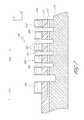
- FIG. 15illustrates a cross-section in the xz plane of the device of FIG. 14 after forming an oxide layer 450 , a polycrystalline silicon layer 452 , and a tungsten silicide layer 454 .
- the blanket oxide layer 450has a thickness between about 50 ⁇ and 80 ⁇ .
- other metallic materialsare used in place of tungsten silicide to strap peripheral gates and improve lateral signal speed.
- an optional blanket silicon nitride layer(not shown) is formed over the tungsten silicide layer 454 .
- the polycrystalline silicon layer 452comprises a conductive material, wherein the term “conductive material” includes silicon, even if undoped as deposited.
- the tungsten silicon layer 454is omitted, and is replaced with additional thickness of the polycrystalline silicon layer 452 .
- This configurationadvantageously removes metal from the structure, thereby reducing the likelihood of introducing contamination into other structures during subsequent processing.
- the metalis added during a subsequent silicidation process.
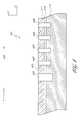
- FIG. 16illustrates a cross-section in the xz plane of the device of FIG. 15 after patterning the blanket-deposited layers.
- the layersare patterned using photolithography and masking techniques.
- one or more active devices 460are formed in the periphery region 310 .
- the active devicescomprise a stack including a gate oxide 462 , a polycrystalline silicon active area 464 , and a tungsten silicide strapping layer 466 .
- the strapping layer 466comprises other metallic materials, such as tungsten, titanium nitride, tantalum, and tantalum nitride. Mixtures of metals are also suitable for forming the strapping layer 466 .
- the same photolithography and masking technique that is used to form active devices 460 in the periphery regionis used to pattern a series of lines 470 in the array region 308 .
- the array lines 470comprise the same materials as the peripheral active devices 460 , although the array lines 470 are used as a sacrificial mask to pattern the underlying elongate loops 112 in subsequent processing steps. Additionally, the pattern of lines 470 in the array region 308 has a smaller pitch as compared to the pattern of active devices 460 in the periphery region 310 .
- the lines 470are spaced apart by a spacing F, wherein the active devices 460 are spaced apart by a spacing 2F, wherein F is the minimum resolvable feature size obtainable using a given photolithography technique.
- the active devices 460have a spacing that is between about two times and about four times larger than the spacing for lines 470 .
- the array lines 470which extend parallel to the y axis, are perpendicular to the elongate loops 112 , which extend parallel to the x axis.
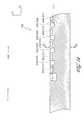
- FIG. 17illustrates a cross-section in the xz plane of the device of FIG. 16 after forming silicon nitride spacers 468 around the active devices 460 in the periphery region 310 .
- the silicon nitride spacers 468have a thickness of between about 200 ⁇ and about 800 ⁇ .
- the silicon nitride spacers 468have a thickness of about 600 ⁇ , and are formed by blanket depositing silicon nitride over the device, followed by a directional etch that removes the deposited material from horizontal surfaces. This technique also results in silicon nitride spacers 468 being formed around the array lines 470 in the array region 308 .
- the silicon nitride spacer material 468fills the region between the lines, thereby forming a pattern of filled gaps 472 between the lines 470 .
- An SOD material 474such as silicon oxide, is formed in the regions of exposed silicon.
- a material other than silicon nitrideis used to form the spacers and filled gaps; other suitable materials include materials that are selectively etched with respect to polycrystalline silicon and silicide materials.
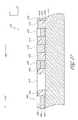
- FIG. 18illustrates a cross-section in the xz plane of the device of FIG. 17 after masking the device periphery region 310 and etching gate mandrels from the device.
- a mask 478is formed over the periphery region 310 to protect the active devices 460 in the periphery region 310 during subsequent processing steps.
- the mask 478is simple as it merely covers the periphery region 310 and opens the array 308 , and therefore does not include “critical dimension” features.
- the remaining portions of the tungsten silicide layer 454 and the polycrystalline silicon layer 452are etched from the exposed portions of the device, such as the array region 308 .
- an etchant that is selective for polycrystalline silicon relative to oxide and nitrideis used, such as tetramethylammonium hydroxide (“TMAH”).
- TMAHtetramethylammonium hydroxide
- Other etchantsare used in other embodiments. This results in the creation of trenches 476 between the nitride material of the filled gaps 472 .
- the siliconis etched to the oxide layer 450 , which acts as an etch stop.
- FIG. 19illustrates a cross-section in the xz plane of the device of FIG. 18 after shrinking the remaining nitride portions of the filled gaps 472 .
- thisis accomplished by isotropically etching nitride from exposed portions of the device.
- the isotropic nitride etchadvantageously creates an area of exposed silicon/dielectric 480 as the remainder of the filled gaps 472 are etched away from the remaining oxide layer 450 .
- the remainder of the filled gaps 472are etched to have a width corresponding to the width of the underlying silicon elongate loops 112 , illustrated in FIG. 14 .
- the remainder of the filled gaps 472are etched to have a width of about 1 ⁇ 2F, where F is the minimum resolvable feature size obtainable using a given photolithography technique.
- FIG. 20illustrates a cross-section in the xz plane of the device of FIG. 19 after etching the pattern of the trenches 476 into the underlying structure illustrated in FIG. 14 .
- the trenches 476are extended to an intermediate depth that is between the depth of the deep trenches 400 and the shallow trenches 404 , illustrated in FIG. 14 .
- the pattern of the intermediate trenches 476is defined by the remaining nitride filled gaps 472 . This effectively cuts the silicon elongate loops 112 , the deep trenches 400 , and the shallow trenches 404 to form a plurality of U-shaped transistor pillars.
- the shallow trenches 404form the middle gap of the U-shaped transistor pillars.
- the U-shaped transistor pillarsfunction source/drain regions for a U-shaped semiconductor structure.
- FIG. 21illustrates a cross-section in the xz plane of the device of FIG. 20 after removing excess nitride material and forming a plurality of sidewall spacers 482 in the intermediate trenches 476 .
- the sidewall spacers 482are separated from the silicon substrate 110 by a thin oxide layer 484 , such as a thermal oxide.
- a portion of the substrate 110 corresponding to the region of the elongate loops 112is doped to include a lightly doped n ⁇ region 486 that is positioned underneath a heavily doped n + region 488 , although p-type doping can be employed in other embodiments.
- a lower portion of the elongate loops 112is doped oppositely from an upper portion of the elongate loops 112 .
- the sidewall spacers 482have a width that is greater than or equal to half of a width of the elongate loops 112 .
- FIG. 22provides a three-dimensional illustration of a portion of the partially-formed semiconductor device of FIG. 21 .
- the deviceincludes a plurality of transistor pillars that form the source 502 and drain 504 regions of a U-shaped transistor 500 .
- the source 502 and drain 504 regionsare separated by a shallow trench 404 which runs parallel to the x axis.
- the channel length of the transistoris the length extending from the source 502 to the drain 504 through the U-shaped channel region 506 .
- the channel characteristics of the deviceare influenced by tailoring the dopant concentrations and types along the channel surfaces on opposite sides of the U-shaped protrusions.
- Neighboring U-shaped transistors 500are separated from each other in the y dimension by deep trenches 400 , and in the x dimension by lined with gate electrode sidewall spacers 482 , which are positioned in the intermediate trenches.
- FIG. 27schematically illustrates the dimensions of a memory cell 520 that is positioned in the array region 308 of a memory device.
- the memory cell 520is located at the intersection of a selected bit line 522 ′ in a bit line array 522 and a selected word line 524 ′ in a word line array 524 .
- the periphery region 310 of the memory deviceoptionally includes logic circuitry 526 that is connected to the bit line array 522 and/or the word line array 524 , as schematically illustrated in FIG. 27 .
- the memory cell 520occupies an area of the substrate 110 having dimensions x ⁇ y, and thus size of the memory cell is generally expressed as xyF 2 , where x and y are multiples of the minimum resolvable feature size F obtainable using a given photolithography technique, as described herein.
- the memory cell 520typically comprises an access device (such as a transistor) and a storage device (such as a capacitor). However, other configurations are used in other embodiments. For example, in a cross-point array the access device can be omitted or an access device can be integrated with the storage device, as in MRAM, EEPROM or PCRAM (for example, silver-doped chalcogenide glass), where the status of a switch acts both as a switch and to store a memory state.
- the memory cell 520is a DRAM cell employing the structure illustrated in FIG. 23 .
- the structure illustrated in FIG. 23includes a single U-shaped transistor 500 having a source 502 and a drain 504 separated by a shallow trench 404 .
- the source 502 and drain 504are connected by a channel region 506 , which is contiguous with the silicon substrate 110 .
- This configurationadvantageously avoids the floating body effect that is common in conventional vertical pillar transistors.
- Gate electrode sidewall spacers 482are formed perpendicular to the shallow trench 404 and loop around both sides of the U-shaped semiconductor (silicon) protrusion.
- a capacitor 510 or other storage deviceis formed over the drain 504 , and an insulated bit line 512 is formed over the source 502 .
- the dimensions of the capacitor 510 and insulated bit line 512are large compared to the dimensions of the pitch-doubled features of the U-shaped transistor 500 .
- the overlying capacitor 510 and insulated bit line 512advantageously accommodate a misalignment of up to 3 ⁇ 8F, wherein F is the minimum resolvable feature size obtainable using a given photolithography technique.
- the memory cell 520occupies a space on the substrate that is preferably between about 4F 2 and about 8F 2 , and is more preferably between about 4F 2 and about 6.5F 2 .
- the configuration of the U-shaped transistor 500advantageously allows the dimensions of the transistors that forms a part of a memory cell to be independently scaled in the x and y dimensions, as illustrated in FIGS. 22 , 23 and 27 .
- thisallows a memory cell occupying an area 6F 2 on the substrate to be formed with a wide variety of different aspect ratios, including a 2.45F ⁇ 2.45F square, a 3F ⁇ 2F rectangle, and 2F ⁇ 3F rectangle.
- the aspect ratio of the transistors comprising the memory deviceis adjustable by manipulating the dimensions of the intermediate trenches 476 and the deep trenches 400 that separate the transistors.
- the capacitor 510 and insulated bit line 512are used to interface the device 100 with other electronic circuitry of a larger system, including other devices which rely on memory such as computers and the like.
- computersoptionally include processors, program logic, and/or other substrate configurations representing data and instructions.
- the processorsoptionally comprise controller circuitry, processor circuitry, processors, general purpose single chip or multiple chip microprocessors, digital signal processors, embedded microprocessors, microcontrollers and the like.
- the device 100is able to be implemented in a wide variety of devices, products and systems.
- wafer contamination and refresh problemsare addressed by eliminating the tungsten silicide layer 454 deposition illustrated in FIG. 15 .
- the tungsten silicide layer 454is replaced with an extended thickness polycrystalline silicon layer, illustrated as layer 464 in FIG. 24 .
- an insulating layer 490such as a SOD material, is blanket deposited over the array region 308 .
- a CMP processis then performed to expose polycrystalline silicon 464 at the tops of the gate stacks in the device periphery region 310 .
- a self-aligned silicidation processis then performed by first depositing a metal layer 492 .
- the resulting structureis illustrated in FIG. 24 .
- a silicidation annealis conducted to react the metal 492 (for example, titanium) in a self-aligned manner where it contacts the polycrystalline silicon layer 464 .
- unreacted metal 492can be selectively etched, as in known in the art.
- between about 500 ⁇ and about 1000 ⁇ of the exposed polycrystalline siliconis converted to titanium silicide.
- Other silicide materialssuch as tungsten silicide, ruthenium silicide, tantalum silicide, cobalt silicide or nickel silicide, are formed in other embodiments.
- This configurationadvantageously allows the metal deposition step illustrated in FIG. 15 to be eliminated, thereby reducing or eliminating metal contamination of the substrate and also simplifying removal of the sacrificial gate material (now just one layer of silicon) in the array 308 .
- the embodiment of FIG. 24takes advantage of the fact that an insulating cap layer (for example, silicon nitride) is not needed for the peripheral transistors, because the dimensions of such transistors are not so tight as to require self-aligned contacts in the region 310 .
- a three-sided U-shaped transistoris formed.
- the shallow trenches 404are filled with a non-silicon oxide filler material, such as silicon nitride, at the stage of FIG. 11 .
- a selective etchis used to remove the filler material from the shallow trenches 404 .
- semiconductor materialis also formed in the shallow trenches 404 . Because the shallow trenches 404 are narrower than the intermediate trenches 476 , the deposition of the sidewall spacers 482 fills the shallow trenches 404 .
- the subsequent spacer etchmerely recesses the gate material within the shallow trenches 404 below the level of the tops of the source/drain regions.
- This processcreates a three-sided transistor structure.
- the gate materialbridges the row of U-shaped protrusions forming the sidewall gate regions on both sides and equalizing potential. Additional details regarding this process are provided in FIGS. 32-35 and the corresponding written description of U.S. patent application Ser. No. 10/933,062 (filed 1 Sep. 2004; Micron Docket 2004-0398.00/US), the entire disclosure of which is hereby incorporated by reference herein.
- the fabrication techniques disclosed hereinadvantageously enable the forming of active devices in the periphery region and the patterning of intermediate trenches in the array region with a single mask.
- a second maskis used to separate the periphery and array regions for different subsequent processing steps.
- this second maskis not critical, and thus is easily aligned over existing structures on the substrate.
- the fabrication techniques disclosed hereinare also applicable to other applications. For example, such techniques are usable to form single transistor, single capacitor DRAM cells.
- the same materials that are used to form active devices in the periphery region 310are also used as sacrificial material for subsequent masking processes in the array region 308 .
- examples of such materialsinclude the polycrystalline silicon layer 452 and optionally, the tungsten silicide layer 454 . This advantageously eliminates the need to use two different critical masks to separately form features in the device periphery region 310 and device array region 308 .
- the material used to form the gate electrode sidewall spacers 482 in the device periphery region 310is also used as a hard mask material in the device array region 308 .
- deposition of the silicon nitride spacers 468fill the gaps between the lines 470 in the array region 308 .
Landscapes
- Engineering & Computer Science (AREA)
- Manufacturing & Machinery (AREA)
- Chemical & Material Sciences (AREA)
- Inorganic Chemistry (AREA)
- Physics & Mathematics (AREA)
- Condensed Matter Physics & Semiconductors (AREA)
- General Physics & Mathematics (AREA)
- Computer Hardware Design (AREA)
- Microelectronics & Electronic Packaging (AREA)
- Power Engineering (AREA)
- Semiconductor Memories (AREA)
Abstract
Description
Claims (11)
Priority Applications (3)
| Application Number | Priority Date | Filing Date | Title |
|---|---|---|---|
| US12/940,948US8207583B2 (en) | 2006-03-02 | 2010-11-05 | Memory device comprising an array portion and a logic portion |
| US13/525,730US8772840B2 (en) | 2006-03-02 | 2012-06-18 | Memory device comprising an array portion and a logic portion |
| US14/297,541US20140284672A1 (en) | 2006-03-02 | 2014-06-05 | Memory device comprising an array portion and a logic portion |
Applications Claiming Priority (2)
| Application Number | Priority Date | Filing Date | Title |
|---|---|---|---|
| US11/367,020US7842558B2 (en) | 2006-03-02 | 2006-03-02 | Masking process for simultaneously patterning separate regions |
| US12/940,948US8207583B2 (en) | 2006-03-02 | 2010-11-05 | Memory device comprising an array portion and a logic portion |
Related Parent Applications (1)
| Application Number | Title | Priority Date | Filing Date |
|---|---|---|---|
| US11/367,020DivisionUS7842558B2 (en) | 2006-03-02 | 2006-03-02 | Masking process for simultaneously patterning separate regions |
Related Child Applications (1)
| Application Number | Title | Priority Date | Filing Date |
|---|---|---|---|
| US13/525,730ContinuationUS8772840B2 (en) | 2006-03-02 | 2012-06-18 | Memory device comprising an array portion and a logic portion |
Publications (2)
| Publication Number | Publication Date |
|---|---|
| US20110042755A1 US20110042755A1 (en) | 2011-02-24 |
| US8207583B2true US8207583B2 (en) | 2012-06-26 |
Family
ID=38470751
Family Applications (4)
| Application Number | Title | Priority Date | Filing Date |
|---|---|---|---|
| US11/367,020Active2026-06-16US7842558B2 (en) | 2006-03-02 | 2006-03-02 | Masking process for simultaneously patterning separate regions |
| US12/940,948ActiveUS8207583B2 (en) | 2006-03-02 | 2010-11-05 | Memory device comprising an array portion and a logic portion |
| US13/525,730ActiveUS8772840B2 (en) | 2006-03-02 | 2012-06-18 | Memory device comprising an array portion and a logic portion |
| US14/297,541AbandonedUS20140284672A1 (en) | 2006-03-02 | 2014-06-05 | Memory device comprising an array portion and a logic portion |
Family Applications Before (1)
| Application Number | Title | Priority Date | Filing Date |
|---|---|---|---|
| US11/367,020Active2026-06-16US7842558B2 (en) | 2006-03-02 | 2006-03-02 | Masking process for simultaneously patterning separate regions |
Family Applications After (2)
| Application Number | Title | Priority Date | Filing Date |
|---|---|---|---|
| US13/525,730ActiveUS8772840B2 (en) | 2006-03-02 | 2012-06-18 | Memory device comprising an array portion and a logic portion |
| US14/297,541AbandonedUS20140284672A1 (en) | 2006-03-02 | 2014-06-05 | Memory device comprising an array portion and a logic portion |
Country Status (1)
| Country | Link |
|---|---|
| US (4) | US7842558B2 (en) |
Cited By (4)
| Publication number | Priority date | Publication date | Assignee | Title |
|---|---|---|---|---|
| US9230967B2 (en)* | 2013-12-18 | 2016-01-05 | Inotera Memories, Inc. | Method for forming self-aligned isolation trenches in semiconductor substrate and semiconductor device |
| US20170110469A1 (en)* | 2015-10-15 | 2017-04-20 | United Microelectronics Corp. | Semiconductor structure and manufacturing method thereof |
| US10354924B2 (en) | 2017-08-30 | 2019-07-16 | Macronix International Co., Ltd. | Semiconductor memory device and method of manufacturing the same |
| US10515801B2 (en) | 2007-06-04 | 2019-12-24 | Micron Technology, Inc. | Pitch multiplication using self-assembling materials |
Families Citing this family (55)
| Publication number | Priority date | Publication date | Assignee | Title |
|---|---|---|---|---|
| US8486287B2 (en)* | 2004-03-19 | 2013-07-16 | The Regents Of The University Of California | Methods for fabrication of positional and compositionally controlled nanostructures on substrate |
| US7476933B2 (en) | 2006-03-02 | 2009-01-13 | Micron Technology, Inc. | Vertical gated access transistor |
| US7902074B2 (en) | 2006-04-07 | 2011-03-08 | Micron Technology, Inc. | Simplified pitch doubling process flow |
| US7488685B2 (en) | 2006-04-25 | 2009-02-10 | Micron Technology, Inc. | Process for improving critical dimension uniformity of integrated circuit arrays |
| US7795149B2 (en) | 2006-06-01 | 2010-09-14 | Micron Technology, Inc. | Masking techniques and contact imprint reticles for dense semiconductor fabrication |
| US8852851B2 (en) | 2006-07-10 | 2014-10-07 | Micron Technology, Inc. | Pitch reduction technology using alternating spacer depositions during the formation of a semiconductor device and systems including same |
| US7611980B2 (en) | 2006-08-30 | 2009-11-03 | Micron Technology, Inc. | Single spacer process for multiplying pitch by a factor greater than two and related intermediate IC structures |
| US7666578B2 (en) | 2006-09-14 | 2010-02-23 | Micron Technology, Inc. | Efficient pitch multiplication process |
| US8563229B2 (en) | 2007-07-31 | 2013-10-22 | Micron Technology, Inc. | Process of semiconductor fabrication with mask overlay on pitch multiplied features and associated structures |
| US7737039B2 (en)* | 2007-11-01 | 2010-06-15 | Micron Technology, Inc. | Spacer process for on pitch contacts and related structures |
| US7659208B2 (en) | 2007-12-06 | 2010-02-09 | Micron Technology, Inc | Method for forming high density patterns |
| US7790531B2 (en) | 2007-12-18 | 2010-09-07 | Micron Technology, Inc. | Methods for isolating portions of a loop of pitch-multiplied material and related structures |
| US7898857B2 (en)* | 2008-03-20 | 2011-03-01 | Micron Technology, Inc. | Memory structure having volatile and non-volatile memory portions |
| US8030218B2 (en) | 2008-03-21 | 2011-10-04 | Micron Technology, Inc. | Method for selectively modifying spacing between pitch multiplied structures |
| US7989307B2 (en) | 2008-05-05 | 2011-08-02 | Micron Technology, Inc. | Methods of forming isolated active areas, trenches, and conductive lines in semiconductor structures and semiconductor structures including the same |
| US10151981B2 (en) | 2008-05-22 | 2018-12-11 | Micron Technology, Inc. | Methods of forming structures supported by semiconductor substrates |
| JP2009295785A (en)* | 2008-06-05 | 2009-12-17 | Toshiba Corp | Method of manufacturing semiconductor device |
| US8076208B2 (en) | 2008-07-03 | 2011-12-13 | Micron Technology, Inc. | Method for forming transistor with high breakdown voltage using pitch multiplication technique |
| US8222159B2 (en)* | 2008-08-25 | 2012-07-17 | Elpida Memory, Inc. | Manufacturing method of semiconductor device |
| US8101497B2 (en) | 2008-09-11 | 2012-01-24 | Micron Technology, Inc. | Self-aligned trench formation |
| US8492282B2 (en) | 2008-11-24 | 2013-07-23 | Micron Technology, Inc. | Methods of forming a masking pattern for integrated circuits |
| US8273634B2 (en) | 2008-12-04 | 2012-09-25 | Micron Technology, Inc. | Methods of fabricating substrates |
| US8796155B2 (en) | 2008-12-04 | 2014-08-05 | Micron Technology, Inc. | Methods of fabricating substrates |
| US8247302B2 (en) | 2008-12-04 | 2012-08-21 | Micron Technology, Inc. | Methods of fabricating substrates |
| US8692310B2 (en) | 2009-02-09 | 2014-04-08 | Spansion Llc | Gate fringing effect based channel formation for semiconductor device |
| US8268543B2 (en) | 2009-03-23 | 2012-09-18 | Micron Technology, Inc. | Methods of forming patterns on substrates |
| US9330934B2 (en) | 2009-05-18 | 2016-05-03 | Micron Technology, Inc. | Methods of forming patterns on substrates |
| US8268730B2 (en)* | 2009-06-03 | 2012-09-18 | Micron Technology, Inc. | Methods of masking semiconductor device structures |
| TWI409852B (en)* | 2009-12-31 | 2013-09-21 | Inotera Memories Inc | Method for fabricating fine patterns of semiconductor device utilizing self-aligned double patterning |
| US8518788B2 (en) | 2010-08-11 | 2013-08-27 | Micron Technology, Inc. | Methods of forming a plurality of capacitors |
| US8574954B2 (en) | 2010-08-31 | 2013-11-05 | Micron Technology, Inc. | Phase change memory structures and methods |
| US8455341B2 (en) | 2010-09-02 | 2013-06-04 | Micron Technology, Inc. | Methods of forming features of integrated circuitry |
| US8575032B2 (en) | 2011-05-05 | 2013-11-05 | Micron Technology, Inc. | Methods of forming a pattern on a substrate |
| US8969154B2 (en)* | 2011-08-23 | 2015-03-03 | Micron Technology, Inc. | Methods for fabricating semiconductor device structures and arrays of vertical transistor devices |
| US9076680B2 (en) | 2011-10-18 | 2015-07-07 | Micron Technology, Inc. | Integrated circuitry, methods of forming capacitors, and methods of forming integrated circuitry comprising an array of capacitors and circuitry peripheral to the array |
| US8962484B2 (en) | 2011-12-16 | 2015-02-24 | Taiwan Semiconductor Manufacturing Company, Ltd. | Method of forming pattern for semiconductor device |
| US9177794B2 (en) | 2012-01-13 | 2015-11-03 | Micron Technology, Inc. | Methods of patterning substrates |
| US8629048B1 (en) | 2012-07-06 | 2014-01-14 | Micron Technology, Inc. | Methods of forming a pattern on a substrate |
| TWI449479B (en)* | 2012-11-01 | 2014-08-11 | Rtr Tech Technology Co Ltd | Method for manufacturing circuit |
| US8735267B1 (en)* | 2012-12-06 | 2014-05-27 | Nanya Technology Corporation | Buried word line structure and method of forming the same |
| US8703577B1 (en)* | 2012-12-17 | 2014-04-22 | United Microelectronics Corp. | Method for fabrication deep trench isolation structure |
| EP2973726A4 (en)* | 2013-03-11 | 2016-11-30 | Crocus Technology Inc | Magnetic random access memory cells with isolating liners |
| US9349808B2 (en)* | 2014-09-29 | 2016-05-24 | International Business Machines Corporation | Double aspect ratio trapping |
| US9508719B2 (en)* | 2014-11-26 | 2016-11-29 | Taiwan Semiconductor Manufacturing Company, Ltd. | Fin field effect transistor (FinFET) device with controlled end-to-end critical dimension and method for forming the same |
| US9397145B1 (en) | 2015-05-14 | 2016-07-19 | Micron Technology, Inc. | Memory structures and related cross-point memory arrays, electronic systems, and methods of forming memory structures |
| US9524974B1 (en)* | 2015-07-22 | 2016-12-20 | Sandisk Technologies Llc | Alternating sidewall assisted patterning |
| US10056395B2 (en) | 2016-03-29 | 2018-08-21 | Macronix International Co., Ltd. | Method of improving localized wafer shape changes |
| KR102301850B1 (en)* | 2016-11-24 | 2021-09-14 | 삼성전자주식회사 | An active pattern structure and a semiconductor device including the same |
| CN111052395A (en) | 2017-08-31 | 2020-04-21 | 美光科技公司 | Semiconductor device, transistor and related method for contacting metal oxide semiconductor device |
| EP3676878A4 (en) | 2017-08-31 | 2020-11-04 | Micron Technology, Inc. | SEMICONDUCTOR COMPONENTS, HYBRID TRANSISTORS AND RELATED PROCESSES |
| US10566531B2 (en) | 2017-11-17 | 2020-02-18 | International Business Machines Corporation | Crosspoint fill-in memory cell with etched access device |
| CN112420722B (en)* | 2019-08-22 | 2022-06-10 | 长鑫存储技术有限公司 | Embedded grid structure and method for forming semiconductor memory |
| US11545543B2 (en) | 2020-10-27 | 2023-01-03 | Taiwan Semiconductor Manufacturing Company, Ltd. | Trench pattern for trench capacitor yield improvement |
| US20230290863A1 (en)* | 2022-03-09 | 2023-09-14 | Taiwan Semiconductor Manufacturing Company Limited | Semiconductor device and methods of formation |
| CN118201366A (en)* | 2022-12-14 | 2024-06-14 | 长江存储科技有限责任公司 | Semiconductor device and method for manufacturing the same |
Citations (228)
| Publication number | Priority date | Publication date | Assignee | Title |
|---|---|---|---|---|
| US4234362A (en) | 1978-11-03 | 1980-11-18 | International Business Machines Corporation | Method for forming an insulator between layers of conductive material |
| US4419809A (en) | 1981-12-30 | 1983-12-13 | International Business Machines Corporation | Fabrication process of sub-micrometer channel length MOSFETs |
| US4432132A (en) | 1981-12-07 | 1984-02-21 | Bell Telephone Laboratories, Incorporated | Formation of sidewall oxide layers by reactive oxygen ion etching to define submicron features |
| US4502914A (en) | 1982-11-13 | 1985-03-05 | International Business Machines Corporation | Method of making structures with dimensions in the sub-micrometer range |
| US4508579A (en) | 1981-03-30 | 1985-04-02 | International Business Machines Corporation | Lateral device structures using self-aligned fabrication techniques |
| US4570325A (en) | 1983-12-16 | 1986-02-18 | Kabushiki Kaisha Toshiba | Manufacturing a field oxide region for a semiconductor device |
| US4648937A (en) | 1985-10-30 | 1987-03-10 | International Business Machines Corporation | Method of preventing asymmetric etching of lines in sub-micrometer range sidewall images transfer |
| EP0227303A2 (en) | 1985-11-25 | 1987-07-01 | Plessey Overseas Limited | Method of manufacturing semiconductor devices having side-wall isolation |
| US4716131A (en) | 1983-11-28 | 1987-12-29 | Nec Corporation | Method of manufacturing semiconductor device having polycrystalline silicon layer with metal silicide film |
| US4776922A (en) | 1987-10-30 | 1988-10-11 | International Business Machines Corporation | Formation of variable-width sidewall structures |
| US4838991A (en) | 1987-10-30 | 1989-06-13 | International Business Machines Corporation | Process for defining organic sidewall structures |
| US5013680A (en) | 1990-07-18 | 1991-05-07 | Micron Technology, Inc. | Process for fabricating a DRAM array having feature widths that transcend the resolution limit of available photolithography |
| US5047117A (en) | 1990-09-26 | 1991-09-10 | Micron Technology, Inc. | Method of forming a narrow self-aligned, annular opening in a masking layer |
| US5053105A (en) | 1990-07-19 | 1991-10-01 | Micron Technology, Inc. | Process for creating an etch mask suitable for deep plasma etches employing self-aligned silicidation of a metal layer masked with a silicon dioxide template |
| US5117027A (en) | 1990-10-31 | 1992-05-26 | Huls Aktiengesellschaft | Process for the preparation of organosilanes containing methacryloyloxy or acryloyloxy groups |
| EP0491408A2 (en) | 1990-11-20 | 1992-06-24 | Consorzio per la Ricerca sulla Microelettronica nel Mezzogiorno - CoRiMMe | Process for making planarized sub-micrometric trenches in integrated circuits |
| DE4236609A1 (en) | 1992-10-29 | 1994-05-05 | Siemens Ag | Method for forming a structure in the surface of a substrate - with an auxiliary structure laterally bounding an initial masking structure, followed by selective removal of masking structure using the auxiliary structure as an etching mask |
| US5315142A (en) | 1992-03-23 | 1994-05-24 | International Business Machines Corporation | High performance trench EEPROM cell |
| US5319753A (en) | 1992-09-29 | 1994-06-07 | Zilog, Inc. | Queued interrupt mechanism with supplementary command/status/message information |
| US5328810A (en) | 1990-05-07 | 1994-07-12 | Micron Technology, Inc. | Method for reducing, by a factor or 2-N, the minimum masking pitch of a photolithographic process |
| US5330879A (en) | 1992-07-16 | 1994-07-19 | Micron Technology, Inc. | Method for fabrication of close-tolerance lines and sharp emission tips on a semiconductor wafer |
| DE4408764A1 (en) | 1993-03-15 | 1994-09-22 | Toshiba Kawasaki Kk | Semiconductor arrangement |
| US5398205A (en) | 1993-05-10 | 1995-03-14 | Nec Corporation | Semiconductor memory device having trench in which word line is buried |
| US5408116A (en) | 1992-08-24 | 1995-04-18 | Hitachi, Ltd. | Grooved gate transistor having source and drain diffused layers with specified groove corner shape |
| US5470661A (en) | 1993-01-07 | 1995-11-28 | International Business Machines Corporation | Diamond-like carbon films from a hydrocarbon helium plasma |
| US5514885A (en) | 1986-10-09 | 1996-05-07 | Myrick; James J. | SOI methods and apparatus |
| US5593813A (en) | 1994-07-14 | 1997-01-14 | Hyundai Electronics Industries Co. Ltd. | Method for forming submicroscopic patterns |
| US5670794A (en) | 1994-10-07 | 1997-09-23 | Micron Technology, Inc. | Thin film transistors |
| US5679591A (en) | 1996-12-16 | 1997-10-21 | Taiwan Semiconductor Manufacturing Company, Ltd | Method of making raised-bitline contactless trenched flash memory cell |
| US5753546A (en) | 1995-06-30 | 1998-05-19 | Hyundai Electronics Industries Co., Ltd. | Method for fabricating metal oxide field effect transistors |
| US5789320A (en) | 1996-04-23 | 1998-08-04 | International Business Machines Corporation | Plating of noble metal electrodes for DRAM and FRAM |
| US5795830A (en) | 1995-06-06 | 1998-08-18 | International Business Machines Corporation | Reducing pitch with continuously adjustable line and space dimensions |
| US5830332A (en) | 1995-01-26 | 1998-11-03 | International Business Machines Corporation | Sputter deposition of hydrogenated amorphous carbon film and applications thereof |
| US5899746A (en) | 1995-09-08 | 1999-05-04 | Sony Corporation | Method of forming pattern |
| US5905285A (en) | 1996-09-12 | 1999-05-18 | Advanced Micro Devices, Inc. | Ultra short trench transistors and process for making same |
| US5981333A (en) | 1997-02-11 | 1999-11-09 | Micron Technology, Inc. | Methods of forming capacitors and DRAM arrays |
| US5998256A (en) | 1996-11-01 | 1999-12-07 | Micron Technology, Inc. | Semiconductor processing methods of forming devices on a substrate, forming device arrays on a substrate, forming conductive lines on a substrate, and forming capacitor arrays on a substrate, and integrated circuitry |
| US6004862A (en) | 1998-01-20 | 1999-12-21 | Advanced Micro Devices, Inc. | Core array and periphery isolation technique |
| US6010946A (en) | 1996-08-21 | 2000-01-04 | Nec Corporation | Semiconductor device with isolation insulating film tapered and method of manufacturing the same |
| US6020255A (en) | 1998-07-13 | 2000-02-01 | Taiwan Semiconductor Manufacturing Company | Dual damascene interconnect process with borderless contact |
| US6042998A (en) | 1993-09-30 | 2000-03-28 | The University Of New Mexico | Method and apparatus for extending spatial frequencies in photolithography images |
| US6057573A (en) | 1998-05-27 | 2000-05-02 | Vanguard International Semiconductor Corporation | Design for high density memory with relaxed metal pitch |
| US6063688A (en) | 1997-09-29 | 2000-05-16 | Intel Corporation | Fabrication of deep submicron structures and quantum wire transistors using hard-mask transistor width definition |
| US6071789A (en) | 1998-11-10 | 2000-06-06 | Vanguard International Semiconductor Corporation | Method for simultaneously fabricating a DRAM capacitor and metal interconnections |
| DE19928781C1 (en) | 1999-06-23 | 2000-07-06 | Siemens Ag | DRAM cell array has deep word line trenches for increasing transistor channel length and has no fixed potential word lines separating adjacent memory cells |
| JP2000208434A (en) | 1999-01-06 | 2000-07-28 | Infineon Technol North America Corp | Patterning method of semiconductor element and semiconductor device |
| US6110837A (en) | 1999-04-28 | 2000-08-29 | Worldwide Semiconductor Manufacturing Corp. | Method for forming a hard mask of half critical dimension |
| US6140172A (en) | 1997-02-11 | 2000-10-31 | Micron Technology, Inc. | Conductive electrical contacts, capacitors, DRAMs, and integrated circuitry, and methods of forming conductive electrical contacts, capacitors, DRAMs and integrated circuitry |
| US6143476A (en) | 1997-12-12 | 2000-11-07 | Applied Materials Inc | Method for high temperature etching of patterned layers using an organic mask stack |
| JP2000357736A (en) | 1999-06-15 | 2000-12-26 | Toshiba Corp | Semiconductor device and manufacturing method thereof |
| US6207490B1 (en) | 1997-12-11 | 2001-03-27 | Samsung Electronics Co., Ltd. | Semiconductor device and method for fabricating the same |
| US6211044B1 (en) | 1999-04-12 | 2001-04-03 | Advanced Micro Devices | Process for fabricating a semiconductor device component using a selective silicidation reaction |
| US6229169B1 (en) | 1997-12-17 | 2001-05-08 | Infineon Technologies Ag | Memory cell configuration, method for fabricating it and methods for operating it |
| US6282113B1 (en) | 1999-09-29 | 2001-08-28 | International Business Machines Corporation | Four F-squared gapless dual layer bitline DRAM array architecture |
| US6288454B1 (en) | 1999-05-13 | 2001-09-11 | Lsi Logic Corporation | Semiconductor wafer having a layer-to-layer alignment mark and method for fabricating the same |
| US6291334B1 (en) | 1997-12-19 | 2001-09-18 | Applied Materials, Inc. | Etch stop layer for dual damascene process |
| US6297554B1 (en) | 2000-03-10 | 2001-10-02 | United Microelectronics Corp. | Dual damascene interconnect structure with reduced parasitic capacitance |
| US6335257B1 (en) | 2000-09-29 | 2002-01-01 | Vanguard International Semiconductor Corporation | Method of making pillar-type structure on semiconductor substrate |
| US6348380B1 (en) | 2000-08-25 | 2002-02-19 | Micron Technology, Inc. | Use of dilute steam ambient for improvement of flash devices |
| US6362057B1 (en) | 1999-10-26 | 2002-03-26 | Motorola, Inc. | Method for forming a semiconductor device |
| US20020042198A1 (en) | 2000-09-20 | 2002-04-11 | Bjarni Bjarnason | Method in etching of a substrate |
| US20020045308A1 (en) | 1996-11-01 | 2002-04-18 | Werner Juengling | Semiconductor processing methods of forming a plurality of capacitors on a substrate, bit line contacts and method of forming bit line contacts |
| US6376893B1 (en)* | 1997-12-13 | 2002-04-23 | Hyundai Electronics Industries Co., Ltd. | Trench isolation structure and fabrication method thereof |
| US6383907B1 (en) | 1999-09-08 | 2002-05-07 | Sony Corporation | Process for fabricating a semiconductor device |
| US20020063110A1 (en) | 2000-11-30 | 2002-05-30 | Cantell Marc W. | Etching of hard masks |
| US20020068243A1 (en) | 2000-12-04 | 2002-06-06 | Jiunn-Ren Hwang | Method of forming opening in wafer layer |
| US6404056B1 (en) | 1994-01-20 | 2002-06-11 | Mitsubishi Denki Kabushiki Kaisha | Semiconductor integrated circuit |
| US20020094688A1 (en) | 2001-01-16 | 2002-07-18 | Semiconductor Leading Edge Technologies, Inc. | Method of forming fine patterns |
| US6423474B1 (en) | 2000-03-21 | 2002-07-23 | Micron Technology, Inc. | Use of DARC and BARC in flash memory processing |
| US20020127810A1 (en) | 2000-05-29 | 2002-09-12 | Fujitsu Limited | Semiconductor device and method for fabricating the same |
| US20020130348A1 (en) | 2001-03-16 | 2002-09-19 | Tran Luan C. | 6F2 dram array, a dram array formed on a semiconductive substrate, a method of forming memory cells in a 6F2 dram array and a method of isolating a single row of memory cells in a 6F2 dram array |
| US6455372B1 (en) | 2000-08-14 | 2002-09-24 | Micron Technology, Inc. | Nucleation for improved flash erase characteristics |
| US20020135029A1 (en) | 2001-03-23 | 2002-09-26 | Er-Xuan Ping | Method for forming raised structures by controlled selective epitaxial growth of facet using spacer |
| US6468887B2 (en) | 1997-04-04 | 2002-10-22 | Nippon Steel Corporation | Semiconductor device and a method of manufacturing the same |
| US20020158273A1 (en) | 2000-10-17 | 2002-10-31 | Hitachi, Ltd. | Nonvolatile semiconductor memory device and a method of manufacturing the same |
| US6475867B1 (en) | 2001-04-02 | 2002-11-05 | Advanced Micro Devices, Inc. | Method of forming integrated circuit features by oxidation of titanium hard mask |
| WO2002099864A1 (en) | 2001-05-31 | 2002-12-12 | Infineon Technologies, Ag | Method for removing polysilane from a semiconductor without stripping |
| US6500756B1 (en) | 2002-06-28 | 2002-12-31 | Advanced Micro Devices, Inc. | Method of forming sub-lithographic spaces between polysilicon lines |
| US6500763B2 (en) | 1999-12-14 | 2002-12-31 | Samsung Electronics Co., Ltd. | Method for manufacturing an electrode of a capacitor |
| US20030006410A1 (en) | 2000-03-01 | 2003-01-09 | Brian Doyle | Quantum wire gate device and method of making same |
| US6514884B2 (en) | 1998-02-06 | 2003-02-04 | Semiconductor Process Laboratory Co., Ltd. | Method for reforming base surface, method for manufacturing semiconductor device and equipment for manufacturing the same |
| US6522584B1 (en) | 2001-08-02 | 2003-02-18 | Micron Technology, Inc. | Programming methods for multi-level flash EEPROMs |
| US20030044722A1 (en) | 2001-08-28 | 2003-03-06 | Yi-Yu Hsu | Process for improving critical dimension uniformity |
| US6534243B1 (en) | 2000-10-23 | 2003-03-18 | Advanced Micro Devices, Inc. | Chemical feature doubling process |
| US6548396B2 (en) | 1998-07-23 | 2003-04-15 | Applied Materials, Inc. | Method of producing an interconnect structure for an integrated circuit |
| US6551878B2 (en) | 1998-09-03 | 2003-04-22 | Micron Technology, Inc. | Mini flash process and circuit |
| US6559017B1 (en) | 2002-06-13 | 2003-05-06 | Advanced Micro Devices, Inc. | Method of using amorphous carbon as spacer material in a disposable spacer process |
| US6558756B2 (en) | 1996-08-29 | 2003-05-06 | Matsushita Electric Industrial Co., Ltd. | Method of forming interlayer insulating film |
| US6566280B1 (en) | 2002-08-26 | 2003-05-20 | Intel Corporation | Forming polymer features on a substrate |
| US6573030B1 (en) | 2000-02-17 | 2003-06-03 | Applied Materials, Inc. | Method for depositing an amorphous carbon layer |
| US20030109102A1 (en) | 2001-10-24 | 2003-06-12 | Hiroshi Kujirai | Method of manufacturing semiconductor device and semiconductor device |
| US20030119307A1 (en) | 2001-12-26 | 2003-06-26 | Applied Materials, Inc. | Method of forming a dual damascene structure |
| US20030129001A1 (en) | 2000-12-28 | 2003-07-10 | Teruaki Kisu | Method of manufacturing semiconductor memory device and semiconductor memory device |
| US20030127426A1 (en) | 2002-01-07 | 2003-07-10 | Macronix International Co., Ltd. | Method for pitch reduction |
| US6597203B2 (en) | 2001-03-14 | 2003-07-22 | Micron Technology, Inc. | CMOS gate array with vertical transistors |
| US6599684B2 (en) | 2001-08-13 | 2003-07-29 | Eastman Kodak Company | Color photothermographic element comprising a dye-forming system for forming a novel infrared dye |
| US6602779B1 (en) | 2002-05-13 | 2003-08-05 | Taiwan Semiconductor Manufacturing Co., Ltd | Method for forming low dielectric constant damascene structure while employing carbon doped silicon oxide planarizing stop layer |
| US20030157436A1 (en) | 2002-02-20 | 2003-08-21 | Dirk Manger | Method for forming a hard mask in a layer on a planar device |
| US6620715B1 (en) | 2002-03-29 | 2003-09-16 | Cypress Semiconductor Corp. | Method for forming sub-critical dimension structures in an integrated circuit |
| US6627933B2 (en) | 2001-04-12 | 2003-09-30 | Micron Technology, Inc. | Method of forming minimally spaced word lines |
| US6632741B1 (en) | 2000-07-19 | 2003-10-14 | International Business Machines Corporation | Self-trimming method on looped patterns |
| EP1357433A2 (en) | 2002-04-23 | 2003-10-29 | Hewlett-Packard Company | Method of fabricating sub-lithographic sized line and space patterns |
| US20030203564A1 (en) | 2002-04-26 | 2003-10-30 | Mcqueen Mark | Methods of forming semiconductor constructions |
| US20030207584A1 (en) | 2002-05-01 | 2003-11-06 | Swaminathan Sivakumar | Patterning tighter and looser pitch geometries |
| US20030207207A1 (en) | 2002-05-03 | 2003-11-06 | Weimin Li | Method of fabricating a semiconductor multilevel interconnect structure |
| US20030216050A1 (en) | 2002-05-17 | 2003-11-20 | International Business Machines Corporation | Method of forming active devices of different gatelengths using lithographic printed gate images of same length |
| US20030215978A1 (en) | 2001-09-19 | 2003-11-20 | Jon Maimon | Method for making tapered opening for programmable resistance memory element |
| US20030230234A1 (en) | 2002-06-14 | 2003-12-18 | Dong-Seok Nam | Method of forming fine patterns of semiconductor device |
| US6667237B1 (en) | 2000-10-12 | 2003-12-23 | Vram Technologies, Llc | Method and apparatus for patterning fine dimensions |
| US20030235076A1 (en) | 2002-06-21 | 2003-12-25 | Micron Technology, Inc. | Multistate NROM having a storage density much greater than 1 Bit per 1F2 |
| WO2004001799A2 (en) | 2002-06-20 | 2003-12-31 | Applied Materials, Inc. | Method for fabricating a gate structure of a field effect transistor |
| US20040000534A1 (en) | 2002-06-28 | 2004-01-01 | Infineon Technologies North America Corp. | Hardmask of amorphous carbon-hydrogen (a-C:H) layers with tunable etch resistivity |
| US6673684B1 (en) | 2002-07-31 | 2004-01-06 | Advanced Micro Devices, Inc. | Use of diamond as a hard mask material |
| US20040018738A1 (en) | 2002-07-22 | 2004-01-29 | Wei Liu | Method for fabricating a notch gate structure of a field effect transistor |
| US20040017989A1 (en) | 2002-07-23 | 2004-01-29 | So Daniel W. | Fabricating sub-resolution structures in planar lightwave devices |
| US6686245B1 (en) | 2002-12-20 | 2004-02-03 | Motorola, Inc. | Vertical MOSFET with asymmetric gate structure |
| US20040023475A1 (en) | 2002-07-31 | 2004-02-05 | Advanced Micro Devices, Inc. | Method for reducing pattern deformation and photoresist poisoning in semiconductor device fabrication |
| US20040023502A1 (en) | 2002-08-02 | 2004-02-05 | Applied Materials Inc. | Undoped and fluorinated amorphous carbon film as pattern mask for metal etch |
| US6689695B1 (en) | 2002-06-28 | 2004-02-10 | Taiwan Semiconductor Manufacturing Company | Multi-purpose composite mask for dual damascene patterning |
| US6693324B2 (en) | 1996-04-26 | 2004-02-17 | Mitsubishi Denki Kabushiki Kaisha | Semiconductor device having a thin film transistor and manufacturing method thereof |
| US20040041189A1 (en) | 2002-08-29 | 2004-03-04 | Voshell Thomas W. | Random access memory device utilizing a vertically oriented select transistor |
| US20040047201A1 (en)* | 1999-06-17 | 2004-03-11 | Hitachi, Ltd. | Semiconductor memory device having self-aligned wiring conductor |
| JP2004080033A (en) | 2002-08-09 | 2004-03-11 | Samsung Electronics Co Ltd | Fine pattern forming method using silicon oxide film |
| US6707092B2 (en) | 2001-07-16 | 2004-03-16 | Masayoshi Sasaki | Semiconductor memory having longitudinal cell structure |
| US6706571B1 (en) | 2002-10-22 | 2004-03-16 | Advanced Micro Devices, Inc. | Method for forming multiple structures in a semiconductor device |
| US20040053475A1 (en) | 2002-09-18 | 2004-03-18 | Gian Sharma | Method for forming a sublithographic opening in a semiconductor process |
| US6709807B2 (en) | 1999-12-02 | 2004-03-23 | Axcelis Technologies, Inc. | Process for reducing edge roughness in patterned photoresist |
| US6713392B1 (en) | 2000-10-05 | 2004-03-30 | Advanced Micro Devices, Inc. | Nitrogen oxide plasma treatment for reduced nickel silicide bridging |
| US20040079988A1 (en) | 2002-10-28 | 2004-04-29 | Sandisk Corporation | Flash memory cell arrays having dual control gates per memory cell charge storage element |
| US6734063B2 (en) | 2002-07-22 | 2004-05-11 | Infineon Technologies Ag | Non-volatile memory cell and fabrication method |
| US6734107B2 (en) | 2002-06-12 | 2004-05-11 | Macronix International Co., Ltd. | Pitch reduction in semiconductor fabrication |
| US6737333B2 (en) | 2001-07-03 | 2004-05-18 | Texas Instruments Incorporated | Semiconductor device isolation structure and method of forming |
| JP2004152784A (en) | 2002-10-28 | 2004-05-27 | Fujitsu Ltd | Method for manufacturing fine pattern and method for manufacturing semiconductor device |
| US6744094B2 (en) | 2001-08-24 | 2004-06-01 | Micron Technology Inc. | Floating gate transistor with horizontal gate layers stacked next to vertical body |
| US20040106257A1 (en) | 2002-04-12 | 2004-06-03 | Matsushita Electric Industrial Co., Ltd. | Method for fabricating semiconductor device |
| US6762449B2 (en) | 1999-04-23 | 2004-07-13 | Hitachi, Ltd. | Semiconductor integrated circuit device and the process of manufacturing the same having poly-silicon plug, wiring trenches and bit lines formed in the wiring trenches having a width finer than a predetermined size |
| US6768663B2 (en) | 1998-09-28 | 2004-07-27 | Texas Instruments Incorporated | Semiconductor device array having dense memory cell array and hierarchical bit line scheme |
| US6773998B1 (en) | 2003-05-20 | 2004-08-10 | Advanced Micro Devices, Inc. | Modified film stack and patterning strategy for stress compensation and prevention of pattern distortion in amorphous carbon gate patterning |
| US6777725B2 (en)* | 2002-06-14 | 2004-08-17 | Ingentix Gmbh & Co. Kg | NROM memory circuit with recessed bitline |
| WO2004073044A2 (en) | 2003-02-13 | 2004-08-26 | Massachusetts Institute Of Technology | Finfet device and method to make same |
| US6794699B2 (en) | 2002-08-29 | 2004-09-21 | Micron Technology Inc | Annular gate and technique for fabricating an annular gate |
| US6800930B2 (en) | 2002-07-31 | 2004-10-05 | Micron Technology, Inc. | Semiconductor dice having back side redistribution layer accessed using through-silicon vias, and assemblies |
| US6818141B1 (en) | 2002-06-10 | 2004-11-16 | Advanced Micro Devices, Inc. | Application of the CVD bilayer ARC as a hard mask for definition of the subresolution trench features between polysilicon wordlines |
| US20040232471A1 (en)* | 2001-09-20 | 2004-11-25 | Shoji Shukuri | Semiconductor integrated circuit device and its manufacturing method |
| US20040235255A1 (en) | 2003-05-21 | 2004-11-25 | Renesas Technology Corp. | Method of manufacturing semiconductor device capable of suppressing impurity concentration reduction in doped channel region arising from formation of gate insulating film |
| US6835662B1 (en) | 2003-07-14 | 2004-12-28 | Advanced Micro Devices, Inc. | Partially de-coupled core and periphery gate module process |
| US6844591B1 (en) | 2003-09-17 | 2005-01-18 | Micron Technology, Inc. | Method of forming DRAM access transistors |
| WO2005010973A1 (en) | 2003-07-18 | 2005-02-03 | Forschungszentrum Jülich GmbH | Method for the self-adjusted reduction in size of structures |
| US6867116B1 (en) | 2003-11-10 | 2005-03-15 | Macronix International Co., Ltd. | Fabrication method of sub-resolution pitch for integrated circuits |
| US6875703B1 (en) | 2004-01-20 | 2005-04-05 | International Business Machines Corporation | Method for forming quadruple density sidewall image transfer (SIT) structures |
| US20050074949A1 (en) | 2003-10-01 | 2005-04-07 | Dongbu Electronics Co., Ltd. | Semiconductor device and a method for fabricating the semiconductor device |
| US20050079662A1 (en) | 2001-12-03 | 2005-04-14 | Hiroshi Miki | Nonvolatile semiconductor storage and its manufacturing method |
| WO2005034215A1 (en) | 2003-09-30 | 2005-04-14 | Infineon Technologies Ag | Method for the production of a hard mask and hard mask arrangement |
| US6881627B2 (en) | 2001-02-09 | 2005-04-19 | Micron Technology, Inc. | Flash memory with ultra thin vertical body transistors |
| US6888187B2 (en) | 2002-08-26 | 2005-05-03 | International Business Machines Corporation | DRAM cell with enhanced SER immunity |
| US6890812B2 (en) | 2001-02-09 | 2005-05-10 | Micron Technology Inc. | Method of forming a memory having a vertical transistor |
| US6890858B2 (en) | 1999-03-23 | 2005-05-10 | Micron Technology, Inc. | Methods of forming materials over uneven surface topologies, and methods of forming insulative materials over and between conductive lines |
| US6893972B2 (en) | 2001-08-31 | 2005-05-17 | Infineon Technologies Ag | Process for sidewall amplification of resist structures and for the production of structures having reduced structure size |
| US20050112886A1 (en) | 2001-12-28 | 2005-05-26 | Kabushiki Kaisha Toshiba | Light-emitting device and method for manufacturing the same |
| US6900521B2 (en) | 2002-06-10 | 2005-05-31 | Micron Technology, Inc. | Vertical transistors and output prediction logic circuits containing same |
| JP2005150333A (en) | 2003-11-14 | 2005-06-09 | Sony Corp | Method of manufacturing semiconductor device |
| US20050142497A1 (en) | 2003-12-26 | 2005-06-30 | Samsung Electronics Co., Ltd. | Method of forming a pattern in a semiconductor device and method of forming a gate using the same |
| US6916594B2 (en) | 2002-12-30 | 2005-07-12 | Hynix Semiconductor Inc. | Overcoating composition for photoresist and method for forming photoresist pattern using the same |
| US20050153562A1 (en) | 2004-01-08 | 2005-07-14 | Toshiharu Furukawa | Method of independent P and N gate length control of FET device made by sidewall image transfer technique |
| US20050151206A1 (en) | 2003-12-30 | 2005-07-14 | Schwerin Ulrike G. | Transistor structure with a curved channel, memory cell and memory cell array for DRAMs, and methods for fabricating a DRAM |
| US20050164454A1 (en) | 2004-01-27 | 2005-07-28 | Micron Technology, Inc. | Selective epitaxy vertical integrated circuit components and methods |
| US20050167394A1 (en) | 2004-01-30 | 2005-08-04 | Wei Liu | Techniques for the use of amorphous carbon (APF) for various etch and litho integration scheme |
| US20050186746A1 (en) | 2004-02-23 | 2005-08-25 | Chul Lee | Method of manufacturing a fin field effect transistor |
| US6936507B2 (en) | 2002-08-15 | 2005-08-30 | Micron Technology, Inc. | Method of forming field effect transistors |
| US20050202672A1 (en) | 2004-03-10 | 2005-09-15 | International Business Machines Corporation | Method for manufacturing tungsten/polysilicon word line structure in vertical dram and device manufactured thereby |
| US20050207264A1 (en) | 1999-04-26 | 2005-09-22 | Taiwan Semiconductor Manufacturing Company | Method to increase coupling ratio of source to floating gate in split-gate flash |
| US6955961B1 (en) | 2004-05-27 | 2005-10-18 | Macronix International Co., Ltd. | Method for defining a minimum pitch in an integrated circuit beyond photolithographic resolution |
| GB2404083B (en) | 2003-07-14 | 2005-11-02 | Samsung Electronics Co Ltd | Integration method of a semiconductor device having a recessed gate electrode |
| US20050272259A1 (en) | 2004-06-08 | 2005-12-08 | Macronix International Co., Ltd. | Method of pitch dimension shrinkage |
| US20060003182A1 (en) | 2004-07-01 | 2006-01-05 | Lane Richard H | Method for forming controlled geometry hardmasks including subresolution elements and resulting structures |
| US20060011947A1 (en)* | 2004-05-26 | 2006-01-19 | Werner Juengling | Semiconductor structures and memory device constructions |
| US20060024940A1 (en) | 2004-07-28 | 2006-02-02 | International Business Machines Corporation | Borderless contact structures |
| US20060022248A1 (en) | 2004-07-28 | 2006-02-02 | Bjorn Fischer | Electronic data memory device for a high read current |
| US20060024945A1 (en) | 2004-07-29 | 2006-02-02 | Hynix Semiconductor, Inc. | Method for fabricating semiconductor device using amorphous carbon layer as sacrificial hard mask |
| US20060028859A1 (en) | 2002-11-12 | 2006-02-09 | Micron Technology, Inc. | 6F2 3-Transistor DRAM gain cell |
| US20060046161A1 (en) | 2004-08-31 | 2006-03-02 | Zhiping Yin | Prevention of photoresist scumming |
| US20060046484A1 (en) | 2004-09-02 | 2006-03-02 | Abatchev Mirzafer K | Method for integrated circuit fabrication using pitch multiplication |
| US20060046407A1 (en) | 2004-09-01 | 2006-03-02 | Werner Juengling | DRAM cells with vertical transistors |
| US20060046200A1 (en) | 2004-09-01 | 2006-03-02 | Abatchev Mirzafer K | Mask material conversion |
| US20060046422A1 (en) | 2004-08-31 | 2006-03-02 | Micron Technology, Inc. | Methods for increasing photo alignment margins |
| US20060046201A1 (en) | 2004-09-02 | 2006-03-02 | Sandhu Gurtej S | Method to align mask patterns |
| US7015124B1 (en) | 2003-04-28 | 2006-03-21 | Advanced Micro Devices, Inc. | Use of amorphous carbon for gate patterning |
| US20060083996A1 (en) | 2004-10-11 | 2006-04-20 | Ho-Chul Kim | Apparatus for exposing a substrate, photomask and modified illuminating system of the apparatus, and method of forming a pattern on a substrate using the apparatus |
| US20060115978A1 (en) | 2004-11-30 | 2006-06-01 | Michael Specht | Charge-trapping memory cell and method for production |
| US7074668B1 (en) | 2004-12-16 | 2006-07-11 | Hynix Semiconductor Inc. | Capacitor of semiconductor device and method for forming the same |
| US7084076B2 (en) | 2003-02-27 | 2006-08-01 | Samsung Electronics, Co., Ltd. | Method for forming silicon dioxide film using siloxane |
| US20060172540A1 (en) | 2005-02-03 | 2006-08-03 | Jeffrey Marks | Reduction of feature critical dimensions using multiple masks |
| US20060172504A1 (en)* | 2005-02-03 | 2006-08-03 | Monolithic System Technology, Inc. | Fabrication process for increased capacitance in an embedded DRAM memory |
| US20060189150A1 (en) | 2005-02-23 | 2006-08-24 | Hynix Semiconductor Inc. | Composition for an organic hard mask and method for forming a pattern on a semiconductor device using the same |
| US7105431B2 (en) | 2003-08-22 | 2006-09-12 | Micron Technology, Inc. | Masking methods |
| US7109544B2 (en) | 2003-02-14 | 2006-09-19 | Infineon Technologies Ag | Architecture for vertical transistor cells and transistor-controlled memory cells |
| US20060211260A1 (en) | 2005-03-15 | 2006-09-21 | Luan Tran | Pitch reduced patterns relative to photolithography features |
| US20060216923A1 (en) | 2005-03-28 | 2006-09-28 | Tran Luan C | Integrated circuit fabrication |
| US20060216293A1 (en) | 2005-03-24 | 2006-09-28 | Couto Fernando J R | TNFalpha-neutralizing antibodies |
| US20060231900A1 (en) | 2005-04-19 | 2006-10-19 | Ji-Young Lee | Semiconductor device having fine contacts and method of fabricating the same |
| US20060263699A1 (en) | 2005-05-23 | 2006-11-23 | Mirzafer Abatchev | Methods for forming arrays of a small, closely spaced features |
| US20060267075A1 (en) | 2005-05-26 | 2006-11-30 | Micron Technology, Inc. | Multi-state memory cell |
| US20060273456A1 (en) | 2005-06-02 | 2006-12-07 | Micron Technology, Inc., A Corporation | Multiple spacer steps for pitch multiplication |
| US20060281266A1 (en) | 2005-06-09 | 2006-12-14 | Wells David H | Method and apparatus for adjusting feature size and position |
| US20060278911A1 (en) | 2005-06-14 | 2006-12-14 | Eppich Anton P | Relaxed-pitch method of aligning active area to digit line |
| JP2006351861A (en) | 2005-06-16 | 2006-12-28 | Toshiba Corp | Manufacturing method of semiconductor device |
| US20070026672A1 (en) | 2005-07-29 | 2007-02-01 | Micron Technology, Inc. | Pitch doubled circuit layout |
| US20070049032A1 (en) | 2005-09-01 | 2007-03-01 | Mirzafer Abatchev | Protective coating for planarization |
| US20070049030A1 (en) | 2005-09-01 | 2007-03-01 | Sandhu Gurtej S | Pitch multiplication spacers and methods of forming the same |
| US20070049040A1 (en) | 2005-03-15 | 2007-03-01 | Micron Technology, Inc., A Corporation | Multiple deposition for integration of spacers in pitch multiplication process |
| US20070048674A1 (en) | 2005-09-01 | 2007-03-01 | Wells David H | Methods for forming arrays of small, closely spaced features |
| US20070049011A1 (en) | 2005-09-01 | 2007-03-01 | Micron Technology, Inc., A Corporation | Method of forming isolated features using pitch multiplication |
| US20070050748A1 (en) | 2005-08-30 | 2007-03-01 | Micron Technology, Inc., A Corporation | Method and algorithm for random half pitched interconnect layout with constant spacing |
| US20070045712A1 (en) | 2005-09-01 | 2007-03-01 | Haller Gordon A | Memory cell layout and process flow |
| US20070049035A1 (en) | 2005-08-31 | 2007-03-01 | Tran Luan C | Method of forming pitch multipled contacts |
| US7202174B1 (en) | 2006-02-02 | 2007-04-10 | Hynix Semiconductor Inc. | Method of forming micro pattern in semiconductor device |
| US7208379B2 (en) | 2004-11-29 | 2007-04-24 | Texas Instruments Incorporated | Pitch multiplication process |
| US20070145450A1 (en) | 2005-12-28 | 2007-06-28 | Fei Wang | DRAM cell design with folded digitline sense amplifier |
| US20070210449A1 (en) | 2006-03-07 | 2007-09-13 | Dirk Caspary | Memory device and an array of conductive lines and methods of making the same |
| US20070215874A1 (en) | 2006-03-17 | 2007-09-20 | Toshiharu Furukawa | Layout and process to contact sub-lithographic structures |
| US20070215960A1 (en) | 2004-03-19 | 2007-09-20 | The Regents Of The University Of California | Methods for Fabrication of Positional and Compositionally Controlled Nanostructures on Substrate |
| US7288445B2 (en) | 2001-06-21 | 2007-10-30 | International Business Machines Corporation | Double gated transistor and method of fabrication |
| US7291560B2 (en) | 2005-08-01 | 2007-11-06 | Infineon Technologies Ag | Method of production pitch fractionizations in semiconductor technology |
| US20070275309A1 (en) | 2006-05-24 | 2007-11-29 | Synopsys, Inc. | Patterning A Single Integrated Circuit Layer Using Multiple Masks And Multiple Masking Layers |
| US20080054350A1 (en) | 2006-09-06 | 2008-03-06 | International Business Machines Corporation | Vertical field effect transistor arrays and methods for fabrication thereof |
| US7368769B2 (en)* | 2004-07-23 | 2008-05-06 | Samsung Electronics Co., Ltd. | MOS transistor having a recessed gate electrode and fabrication method thereof |
| US20080292991A1 (en) | 2007-05-24 | 2008-11-27 | Advanced Micro Devices, Inc. | High fidelity multiple resist patterning |
| US7851135B2 (en) | 2007-11-30 | 2010-12-14 | Hynix Semiconductor Inc. | Method of forming an etching mask pattern from developed negative and positive photoresist layers |
Family Cites Families (2)
| Publication number | Priority date | Publication date | Assignee | Title |
|---|---|---|---|---|
| US20060192249A1 (en)* | 2004-09-20 | 2006-08-31 | Samsung Electronics Co., Ltd. | Field effect transistors with vertically oriented gate electrodes and methods for fabricating the same |
| US7704198B2 (en)* | 2003-10-14 | 2010-04-27 | Brown Jr Gordon L | Variable resistance exercise device |
- 2006
- 2006-03-02USUS11/367,020patent/US7842558B2/enactiveActive
- 2010
- 2010-11-05USUS12/940,948patent/US8207583B2/enactiveActive
- 2012
- 2012-06-18USUS13/525,730patent/US8772840B2/enactiveActive
- 2014
- 2014-06-05USUS14/297,541patent/US20140284672A1/ennot_activeAbandoned
Patent Citations (257)
| Publication number | Priority date | Publication date | Assignee | Title |
|---|---|---|---|---|
| US4234362A (en) | 1978-11-03 | 1980-11-18 | International Business Machines Corporation | Method for forming an insulator between layers of conductive material |
| US4508579A (en) | 1981-03-30 | 1985-04-02 | International Business Machines Corporation | Lateral device structures using self-aligned fabrication techniques |
| US4432132A (en) | 1981-12-07 | 1984-02-21 | Bell Telephone Laboratories, Incorporated | Formation of sidewall oxide layers by reactive oxygen ion etching to define submicron features |
| US4419809A (en) | 1981-12-30 | 1983-12-13 | International Business Machines Corporation | Fabrication process of sub-micrometer channel length MOSFETs |
| US4502914A (en) | 1982-11-13 | 1985-03-05 | International Business Machines Corporation | Method of making structures with dimensions in the sub-micrometer range |
| US4716131A (en) | 1983-11-28 | 1987-12-29 | Nec Corporation | Method of manufacturing semiconductor device having polycrystalline silicon layer with metal silicide film |
| US4570325A (en) | 1983-12-16 | 1986-02-18 | Kabushiki Kaisha Toshiba | Manufacturing a field oxide region for a semiconductor device |
| US4648937A (en) | 1985-10-30 | 1987-03-10 | International Business Machines Corporation | Method of preventing asymmetric etching of lines in sub-micrometer range sidewall images transfer |
| EP0227303A2 (en) | 1985-11-25 | 1987-07-01 | Plessey Overseas Limited | Method of manufacturing semiconductor devices having side-wall isolation |
| US5514885A (en) | 1986-10-09 | 1996-05-07 | Myrick; James J. | SOI methods and apparatus |
| US4838991A (en) | 1987-10-30 | 1989-06-13 | International Business Machines Corporation | Process for defining organic sidewall structures |
| US4776922A (en) | 1987-10-30 | 1988-10-11 | International Business Machines Corporation | Formation of variable-width sidewall structures |
| US5328810A (en) | 1990-05-07 | 1994-07-12 | Micron Technology, Inc. | Method for reducing, by a factor or 2-N, the minimum masking pitch of a photolithographic process |
| US5013680A (en) | 1990-07-18 | 1991-05-07 | Micron Technology, Inc. | Process for fabricating a DRAM array having feature widths that transcend the resolution limit of available photolithography |
| US5053105A (en) | 1990-07-19 | 1991-10-01 | Micron Technology, Inc. | Process for creating an etch mask suitable for deep plasma etches employing self-aligned silicidation of a metal layer masked with a silicon dioxide template |
| US5047117A (en) | 1990-09-26 | 1991-09-10 | Micron Technology, Inc. | Method of forming a narrow self-aligned, annular opening in a masking layer |
| US5117027A (en) | 1990-10-31 | 1992-05-26 | Huls Aktiengesellschaft | Process for the preparation of organosilanes containing methacryloyloxy or acryloyloxy groups |
| EP0491408A2 (en) | 1990-11-20 | 1992-06-24 | Consorzio per la Ricerca sulla Microelettronica nel Mezzogiorno - CoRiMMe | Process for making planarized sub-micrometric trenches in integrated circuits |
| US5315142A (en) | 1992-03-23 | 1994-05-24 | International Business Machines Corporation | High performance trench EEPROM cell |
| US5330879A (en) | 1992-07-16 | 1994-07-19 | Micron Technology, Inc. | Method for fabrication of close-tolerance lines and sharp emission tips on a semiconductor wafer |
| US5408116A (en) | 1992-08-24 | 1995-04-18 | Hitachi, Ltd. | Grooved gate transistor having source and drain diffused layers with specified groove corner shape |
| US5319753A (en) | 1992-09-29 | 1994-06-07 | Zilog, Inc. | Queued interrupt mechanism with supplementary command/status/message information |
| DE4236609A1 (en) | 1992-10-29 | 1994-05-05 | Siemens Ag | Method for forming a structure in the surface of a substrate - with an auxiliary structure laterally bounding an initial masking structure, followed by selective removal of masking structure using the auxiliary structure as an etching mask |
| US5470661A (en) | 1993-01-07 | 1995-11-28 | International Business Machines Corporation | Diamond-like carbon films from a hydrocarbon helium plasma |
| US5502320A (en) | 1993-03-15 | 1996-03-26 | Kabushiki Kaisha Toshiba | Dynamic random access memory (DRAM) semiconductor device |
| DE4408764A1 (en) | 1993-03-15 | 1994-09-22 | Toshiba Kawasaki Kk | Semiconductor arrangement |
| US5398205A (en) | 1993-05-10 | 1995-03-14 | Nec Corporation | Semiconductor memory device having trench in which word line is buried |
| US6042998A (en) | 1993-09-30 | 2000-03-28 | The University Of New Mexico | Method and apparatus for extending spatial frequencies in photolithography images |
| US6404056B1 (en) | 1994-01-20 | 2002-06-11 | Mitsubishi Denki Kabushiki Kaisha | Semiconductor integrated circuit |
| US5593813A (en) | 1994-07-14 | 1997-01-14 | Hyundai Electronics Industries Co. Ltd. | Method for forming submicroscopic patterns |
| US5670794A (en) | 1994-10-07 | 1997-09-23 | Micron Technology, Inc. | Thin film transistors |
| US5830332A (en) | 1995-01-26 | 1998-11-03 | International Business Machines Corporation | Sputter deposition of hydrogenated amorphous carbon film and applications thereof |
| US5795830A (en) | 1995-06-06 | 1998-08-18 | International Business Machines Corporation | Reducing pitch with continuously adjustable line and space dimensions |
| US5753546A (en) | 1995-06-30 | 1998-05-19 | Hyundai Electronics Industries Co., Ltd. | Method for fabricating metal oxide field effect transistors |
| US5899746A (en) | 1995-09-08 | 1999-05-04 | Sony Corporation | Method of forming pattern |
| US5789320A (en) | 1996-04-23 | 1998-08-04 | International Business Machines Corporation | Plating of noble metal electrodes for DRAM and FRAM |
| US6693324B2 (en) | 1996-04-26 | 2004-02-17 | Mitsubishi Denki Kabushiki Kaisha | Semiconductor device having a thin film transistor and manufacturing method thereof |
| US6010946A (en) | 1996-08-21 | 2000-01-04 | Nec Corporation | Semiconductor device with isolation insulating film tapered and method of manufacturing the same |
| US6558756B2 (en) | 1996-08-29 | 2003-05-06 | Matsushita Electric Industrial Co., Ltd. | Method of forming interlayer insulating film |
| US5905285A (en) | 1996-09-12 | 1999-05-18 | Advanced Micro Devices, Inc. | Ultra short trench transistors and process for making same |
| US5998256A (en) | 1996-11-01 | 1999-12-07 | Micron Technology, Inc. | Semiconductor processing methods of forming devices on a substrate, forming device arrays on a substrate, forming conductive lines on a substrate, and forming capacitor arrays on a substrate, and integrated circuitry |
| US20020045308A1 (en) | 1996-11-01 | 2002-04-18 | Werner Juengling | Semiconductor processing methods of forming a plurality of capacitors on a substrate, bit line contacts and method of forming bit line contacts |
| US5679591A (en) | 1996-12-16 | 1997-10-21 | Taiwan Semiconductor Manufacturing Company, Ltd | Method of making raised-bitline contactless trenched flash memory cell |
| US5981333A (en) | 1997-02-11 | 1999-11-09 | Micron Technology, Inc. | Methods of forming capacitors and DRAM arrays |
| US6140172A (en) | 1997-02-11 | 2000-10-31 | Micron Technology, Inc. | Conductive electrical contacts, capacitors, DRAMs, and integrated circuitry, and methods of forming conductive electrical contacts, capacitors, DRAMs and integrated circuitry |
| US6468887B2 (en) | 1997-04-04 | 2002-10-22 | Nippon Steel Corporation | Semiconductor device and a method of manufacturing the same |
| US6063688A (en) | 1997-09-29 | 2000-05-16 | Intel Corporation | Fabrication of deep submicron structures and quantum wire transistors using hard-mask transistor width definition |
| US6207490B1 (en) | 1997-12-11 | 2001-03-27 | Samsung Electronics Co., Ltd. | Semiconductor device and method for fabricating the same |
| US6143476A (en) | 1997-12-12 | 2000-11-07 | Applied Materials Inc | Method for high temperature etching of patterned layers using an organic mask stack |
| US6376893B1 (en)* | 1997-12-13 | 2002-04-23 | Hyundai Electronics Industries Co., Ltd. | Trench isolation structure and fabrication method thereof |
| US6229169B1 (en) | 1997-12-17 | 2001-05-08 | Infineon Technologies Ag | Memory cell configuration, method for fabricating it and methods for operating it |
| US6291334B1 (en) | 1997-12-19 | 2001-09-18 | Applied Materials, Inc. | Etch stop layer for dual damascene process |
| US6004862A (en) | 1998-01-20 | 1999-12-21 | Advanced Micro Devices, Inc. | Core array and periphery isolation technique |
| US6514884B2 (en) | 1998-02-06 | 2003-02-04 | Semiconductor Process Laboratory Co., Ltd. | Method for reforming base surface, method for manufacturing semiconductor device and equipment for manufacturing the same |
| US6057573A (en) | 1998-05-27 | 2000-05-02 | Vanguard International Semiconductor Corporation | Design for high density memory with relaxed metal pitch |
| US6020255A (en) | 1998-07-13 | 2000-02-01 | Taiwan Semiconductor Manufacturing Company | Dual damascene interconnect process with borderless contact |
| US6548396B2 (en) | 1998-07-23 | 2003-04-15 | Applied Materials, Inc. | Method of producing an interconnect structure for an integrated circuit |
| US6551878B2 (en) | 1998-09-03 | 2003-04-22 | Micron Technology, Inc. | Mini flash process and circuit |
| US6768663B2 (en) | 1998-09-28 | 2004-07-27 | Texas Instruments Incorporated | Semiconductor device array having dense memory cell array and hierarchical bit line scheme |
| US6071789A (en) | 1998-11-10 | 2000-06-06 | Vanguard International Semiconductor Corporation | Method for simultaneously fabricating a DRAM capacitor and metal interconnections |
| JP2000208434A (en) | 1999-01-06 | 2000-07-28 | Infineon Technol North America Corp | Patterning method of semiconductor element and semiconductor device |
| US6890858B2 (en) | 1999-03-23 | 2005-05-10 | Micron Technology, Inc. | Methods of forming materials over uneven surface topologies, and methods of forming insulative materials over and between conductive lines |
| US6211044B1 (en) | 1999-04-12 | 2001-04-03 | Advanced Micro Devices | Process for fabricating a semiconductor device component using a selective silicidation reaction |
| US6762449B2 (en) | 1999-04-23 | 2004-07-13 | Hitachi, Ltd. | Semiconductor integrated circuit device and the process of manufacturing the same having poly-silicon plug, wiring trenches and bit lines formed in the wiring trenches having a width finer than a predetermined size |
| US20050207264A1 (en) | 1999-04-26 | 2005-09-22 | Taiwan Semiconductor Manufacturing Company | Method to increase coupling ratio of source to floating gate in split-gate flash |
| US6110837A (en) | 1999-04-28 | 2000-08-29 | Worldwide Semiconductor Manufacturing Corp. | Method for forming a hard mask of half critical dimension |
| US6288454B1 (en) | 1999-05-13 | 2001-09-11 | Lsi Logic Corporation | Semiconductor wafer having a layer-to-layer alignment mark and method for fabricating the same |
| JP2000357736A (en) | 1999-06-15 | 2000-12-26 | Toshiba Corp | Semiconductor device and manufacturing method thereof |
| US20040047201A1 (en)* | 1999-06-17 | 2004-03-11 | Hitachi, Ltd. | Semiconductor memory device having self-aligned wiring conductor |
| WO2001001489A1 (en) | 1999-06-23 | 2001-01-04 | Infineon Technologies Ag | Dram cell arrangement and method for the production thereof |
| DE19928781C1 (en) | 1999-06-23 | 2000-07-06 | Siemens Ag | DRAM cell array has deep word line trenches for increasing transistor channel length and has no fixed potential word lines separating adjacent memory cells |
| US6383907B1 (en) | 1999-09-08 | 2002-05-07 | Sony Corporation | Process for fabricating a semiconductor device |
| US6282113B1 (en) | 1999-09-29 | 2001-08-28 | International Business Machines Corporation | Four F-squared gapless dual layer bitline DRAM array architecture |
| US6362057B1 (en) | 1999-10-26 | 2002-03-26 | Motorola, Inc. | Method for forming a semiconductor device |
| US6709807B2 (en) | 1999-12-02 | 2004-03-23 | Axcelis Technologies, Inc. | Process for reducing edge roughness in patterned photoresist |
| US6500763B2 (en) | 1999-12-14 | 2002-12-31 | Samsung Electronics Co., Ltd. | Method for manufacturing an electrode of a capacitor |
| US6573030B1 (en) | 2000-02-17 | 2003-06-03 | Applied Materials, Inc. | Method for depositing an amorphous carbon layer |
| US7183597B2 (en) | 2000-03-01 | 2007-02-27 | Intel Corporation | Quantum wire gate device and method of making same |
| US20030006410A1 (en) | 2000-03-01 | 2003-01-09 | Brian Doyle | Quantum wire gate device and method of making same |
| US6297554B1 (en) | 2000-03-10 | 2001-10-02 | United Microelectronics Corp. | Dual damascene interconnect structure with reduced parasitic capacitance |
| US6423474B1 (en) | 2000-03-21 | 2002-07-23 | Micron Technology, Inc. | Use of DARC and BARC in flash memory processing |
| US20020127810A1 (en) | 2000-05-29 | 2002-09-12 | Fujitsu Limited | Semiconductor device and method for fabricating the same |
| US6632741B1 (en) | 2000-07-19 | 2003-10-14 | International Business Machines Corporation | Self-trimming method on looped patterns |
| US6455372B1 (en) | 2000-08-14 | 2002-09-24 | Micron Technology, Inc. | Nucleation for improved flash erase characteristics |
| US6348380B1 (en) | 2000-08-25 | 2002-02-19 | Micron Technology, Inc. | Use of dilute steam ambient for improvement of flash devices |
| US6395613B1 (en) | 2000-08-30 | 2002-05-28 | Micron Technology, Inc. | Semiconductor processing methods of forming a plurality of capacitors on a substrate, bit line contacts and method of forming bit line contacts |
| US20020042198A1 (en) | 2000-09-20 | 2002-04-11 | Bjarni Bjarnason | Method in etching of a substrate |
| US6335257B1 (en) | 2000-09-29 | 2002-01-01 | Vanguard International Semiconductor Corporation | Method of making pillar-type structure on semiconductor substrate |
| US6713392B1 (en) | 2000-10-05 | 2004-03-30 | Advanced Micro Devices, Inc. | Nitrogen oxide plasma treatment for reduced nickel silicide bridging |
| US6667237B1 (en) | 2000-10-12 | 2003-12-23 | Vram Technologies, Llc | Method and apparatus for patterning fine dimensions |
| US20020158273A1 (en) | 2000-10-17 | 2002-10-31 | Hitachi, Ltd. | Nonvolatile semiconductor memory device and a method of manufacturing the same |
| US6534243B1 (en) | 2000-10-23 | 2003-03-18 | Advanced Micro Devices, Inc. | Chemical feature doubling process |
| US20020063110A1 (en) | 2000-11-30 | 2002-05-30 | Cantell Marc W. | Etching of hard masks |
| US20020068243A1 (en) | 2000-12-04 | 2002-06-06 | Jiunn-Ren Hwang | Method of forming opening in wafer layer |
| US20030129001A1 (en) | 2000-12-28 | 2003-07-10 | Teruaki Kisu | Method of manufacturing semiconductor memory device and semiconductor memory device |
| US20020094688A1 (en) | 2001-01-16 | 2002-07-18 | Semiconductor Leading Edge Technologies, Inc. | Method of forming fine patterns |
| US6881627B2 (en) | 2001-02-09 | 2005-04-19 | Micron Technology, Inc. | Flash memory with ultra thin vertical body transistors |
| US6890812B2 (en) | 2001-02-09 | 2005-05-10 | Micron Technology Inc. | Method of forming a memory having a vertical transistor |
| US6597203B2 (en) | 2001-03-14 | 2003-07-22 | Micron Technology, Inc. | CMOS gate array with vertical transistors |
| US20020130348A1 (en) | 2001-03-16 | 2002-09-19 | Tran Luan C. | 6F2 dram array, a dram array formed on a semiconductive substrate, a method of forming memory cells in a 6F2 dram array and a method of isolating a single row of memory cells in a 6F2 dram array |
| US20030164513A1 (en) | 2001-03-23 | 2003-09-04 | Micron Technology, Inc. | Method for forming raised structures by controlled selective epitaxial growth of facet using spacer |
| US20020135029A1 (en) | 2001-03-23 | 2002-09-26 | Er-Xuan Ping | Method for forming raised structures by controlled selective epitaxial growth of facet using spacer |
| US6475867B1 (en) | 2001-04-02 | 2002-11-05 | Advanced Micro Devices, Inc. | Method of forming integrated circuit features by oxidation of titanium hard mask |
| US6627933B2 (en) | 2001-04-12 | 2003-09-30 | Micron Technology, Inc. | Method of forming minimally spaced word lines |
| WO2002099864A1 (en) | 2001-05-31 | 2002-12-12 | Infineon Technologies, Ag | Method for removing polysilane from a semiconductor without stripping |
| US7288445B2 (en) | 2001-06-21 | 2007-10-30 | International Business Machines Corporation | Double gated transistor and method of fabrication |
| US6737333B2 (en) | 2001-07-03 | 2004-05-18 | Texas Instruments Incorporated | Semiconductor device isolation structure and method of forming |
| US6707092B2 (en) | 2001-07-16 | 2004-03-16 | Masayoshi Sasaki | Semiconductor memory having longitudinal cell structure |
| US6522584B1 (en) | 2001-08-02 | 2003-02-18 | Micron Technology, Inc. | Programming methods for multi-level flash EEPROMs |
| US6599684B2 (en) | 2001-08-13 | 2003-07-29 | Eastman Kodak Company | Color photothermographic element comprising a dye-forming system for forming a novel infrared dye |
| US6744094B2 (en) | 2001-08-24 | 2004-06-01 | Micron Technology Inc. | Floating gate transistor with horizontal gate layers stacked next to vertical body |
| US20030044722A1 (en) | 2001-08-28 | 2003-03-06 | Yi-Yu Hsu | Process for improving critical dimension uniformity |
| US6846618B2 (en) | 2001-08-28 | 2005-01-25 | Winbond Electronics Corporation | Process for improving critical dimension uniformity |
| US6893972B2 (en) | 2001-08-31 | 2005-05-17 | Infineon Technologies Ag | Process for sidewall amplification of resist structures and for the production of structures having reduced structure size |
| US20030215978A1 (en) | 2001-09-19 | 2003-11-20 | Jon Maimon | Method for making tapered opening for programmable resistance memory element |
| US20040232471A1 (en)* | 2001-09-20 | 2004-11-25 | Shoji Shukuri | Semiconductor integrated circuit device and its manufacturing method |
| US20030109102A1 (en) | 2001-10-24 | 2003-06-12 | Hiroshi Kujirai | Method of manufacturing semiconductor device and semiconductor device |
| US20050079662A1 (en) | 2001-12-03 | 2005-04-14 | Hiroshi Miki | Nonvolatile semiconductor storage and its manufacturing method |
| US20030119307A1 (en) | 2001-12-26 | 2003-06-26 | Applied Materials, Inc. | Method of forming a dual damascene structure |
| US20050112886A1 (en) | 2001-12-28 | 2005-05-26 | Kabushiki Kaisha Toshiba | Light-emitting device and method for manufacturing the same |
| US20030127426A1 (en) | 2002-01-07 | 2003-07-10 | Macronix International Co., Ltd. | Method for pitch reduction |
| US6638441B2 (en) | 2002-01-07 | 2003-10-28 | Macronix International Co., Ltd. | Method for pitch reduction |
| US20030157436A1 (en) | 2002-02-20 | 2003-08-21 | Dirk Manger | Method for forming a hard mask in a layer on a planar device |
| US7005240B2 (en) | 2002-02-20 | 2006-02-28 | Infineon Technologies Ag | Method for forming a hard mask in a layer on a planar device |
| US6620715B1 (en) | 2002-03-29 | 2003-09-16 | Cypress Semiconductor Corp. | Method for forming sub-critical dimension structures in an integrated circuit |
| US20040106257A1 (en) | 2002-04-12 | 2004-06-03 | Matsushita Electric Industrial Co., Ltd. | Method for fabricating semiconductor device |
| EP1357433A2 (en) | 2002-04-23 | 2003-10-29 | Hewlett-Packard Company | Method of fabricating sub-lithographic sized line and space patterns |
| US20030203564A1 (en) | 2002-04-26 | 2003-10-30 | Mcqueen Mark | Methods of forming semiconductor constructions |
| US20030207584A1 (en) | 2002-05-01 | 2003-11-06 | Swaminathan Sivakumar | Patterning tighter and looser pitch geometries |
| US20030207207A1 (en) | 2002-05-03 | 2003-11-06 | Weimin Li | Method of fabricating a semiconductor multilevel interconnect structure |
| US6951709B2 (en) | 2002-05-03 | 2005-10-04 | Micron Technology, Inc. | Method of fabricating a semiconductor multilevel interconnect structure |
| US6602779B1 (en) | 2002-05-13 | 2003-08-05 | Taiwan Semiconductor Manufacturing Co., Ltd | Method for forming low dielectric constant damascene structure while employing carbon doped silicon oxide planarizing stop layer |
| US20030216050A1 (en) | 2002-05-17 | 2003-11-20 | International Business Machines Corporation | Method of forming active devices of different gatelengths using lithographic printed gate images of same length |
| US6818141B1 (en) | 2002-06-10 | 2004-11-16 | Advanced Micro Devices, Inc. | Application of the CVD bilayer ARC as a hard mask for definition of the subresolution trench features between polysilicon wordlines |
| US6900521B2 (en) | 2002-06-10 | 2005-05-31 | Micron Technology, Inc. | Vertical transistors and output prediction logic circuits containing same |
| US6734107B2 (en) | 2002-06-12 | 2004-05-11 | Macronix International Co., Ltd. | Pitch reduction in semiconductor fabrication |
| US6559017B1 (en) | 2002-06-13 | 2003-05-06 | Advanced Micro Devices, Inc. | Method of using amorphous carbon as spacer material in a disposable spacer process |
| US20030230234A1 (en) | 2002-06-14 | 2003-12-18 | Dong-Seok Nam | Method of forming fine patterns of semiconductor device |
| US6777725B2 (en)* | 2002-06-14 | 2004-08-17 | Ingentix Gmbh & Co. Kg | NROM memory circuit with recessed bitline |
| WO2004001799A2 (en) | 2002-06-20 | 2003-12-31 | Applied Materials, Inc. | Method for fabricating a gate structure of a field effect transistor |
| US20040043623A1 (en) | 2002-06-20 | 2004-03-04 | Wei Liu | Method for fabricating a gate structure of a field effect transistor |
| US6924191B2 (en) | 2002-06-20 | 2005-08-02 | Applied Materials, Inc. | Method for fabricating a gate structure of a field effect transistor |
| US20030235076A1 (en) | 2002-06-21 | 2003-12-25 | Micron Technology, Inc. | Multistate NROM having a storage density much greater than 1 Bit per 1F2 |
| US6500756B1 (en) | 2002-06-28 | 2002-12-31 | Advanced Micro Devices, Inc. | Method of forming sub-lithographic spaces between polysilicon lines |
| US20040000534A1 (en) | 2002-06-28 | 2004-01-01 | Infineon Technologies North America Corp. | Hardmask of amorphous carbon-hydrogen (a-C:H) layers with tunable etch resistivity |
| US6689695B1 (en) | 2002-06-28 | 2004-02-10 | Taiwan Semiconductor Manufacturing Company | Multi-purpose composite mask for dual damascene patterning |
| US6835663B2 (en) | 2002-06-28 | 2004-12-28 | Infineon Technologies Ag | Hardmask of amorphous carbon-hydrogen (a-C:H) layers with tunable etch resistivity |
| US20040018738A1 (en) | 2002-07-22 | 2004-01-29 | Wei Liu | Method for fabricating a notch gate structure of a field effect transistor |
| US6734063B2 (en) | 2002-07-22 | 2004-05-11 | Infineon Technologies Ag | Non-volatile memory cell and fabrication method |
| US20040017989A1 (en) | 2002-07-23 | 2004-01-29 | So Daniel W. | Fabricating sub-resolution structures in planar lightwave devices |
| US6764949B2 (en) | 2002-07-31 | 2004-07-20 | Advanced Micro Devices, Inc. | Method for reducing pattern deformation and photoresist poisoning in semiconductor device fabrication |
| US6673684B1 (en) | 2002-07-31 | 2004-01-06 | Advanced Micro Devices, Inc. | Use of diamond as a hard mask material |
| US20050186705A1 (en) | 2002-07-31 | 2005-08-25 | Jackson Timothy L. | Semiconductor dice having backside redistribution layer accessed using through-silicon vias, methods |
| US6800930B2 (en) | 2002-07-31 | 2004-10-05 | Micron Technology, Inc. | Semiconductor dice having back side redistribution layer accessed using through-silicon vias, and assemblies |
| US6962867B2 (en) | 2002-07-31 | 2005-11-08 | Microntechnology, Inc. | Methods of fabrication of semiconductor dice having back side redistribution layer accessed using through-silicon vias and assemblies thereof |
| US20040023475A1 (en) | 2002-07-31 | 2004-02-05 | Advanced Micro Devices, Inc. | Method for reducing pattern deformation and photoresist poisoning in semiconductor device fabrication |
| US6939808B2 (en) | 2002-08-02 | 2005-09-06 | Applied Materials, Inc. | Undoped and fluorinated amorphous carbon film as pattern mask for metal etch |
| US20040023502A1 (en) | 2002-08-02 | 2004-02-05 | Applied Materials Inc. | Undoped and fluorinated amorphous carbon film as pattern mask for metal etch |
| JP2004080033A (en) | 2002-08-09 | 2004-03-11 | Samsung Electronics Co Ltd | Fine pattern forming method using silicon oxide film |
| US6936507B2 (en) | 2002-08-15 | 2005-08-30 | Micron Technology, Inc. | Method of forming field effect transistors |
| US6888187B2 (en) | 2002-08-26 | 2005-05-03 | International Business Machines Corporation | DRAM cell with enhanced SER immunity |
| US6566280B1 (en) | 2002-08-26 | 2003-05-20 | Intel Corporation | Forming polymer features on a substrate |
| US20040041189A1 (en) | 2002-08-29 | 2004-03-04 | Voshell Thomas W. | Random access memory device utilizing a vertically oriented select transistor |
| US6794699B2 (en) | 2002-08-29 | 2004-09-21 | Micron Technology Inc | Annular gate and technique for fabricating an annular gate |
| US6756284B2 (en) | 2002-09-18 | 2004-06-29 | Silicon Storage Technology, Inc. | Method for forming a sublithographic opening in a semiconductor process |
| US20040053475A1 (en) | 2002-09-18 | 2004-03-18 | Gian Sharma | Method for forming a sublithographic opening in a semiconductor process |
| US6706571B1 (en) | 2002-10-22 | 2004-03-16 | Advanced Micro Devices, Inc. | Method for forming multiple structures in a semiconductor device |
| US20040079988A1 (en) | 2002-10-28 | 2004-04-29 | Sandisk Corporation | Flash memory cell arrays having dual control gates per memory cell charge storage element |
| JP2004152784A (en) | 2002-10-28 | 2004-05-27 | Fujitsu Ltd | Method for manufacturing fine pattern and method for manufacturing semiconductor device |
| US20060028859A1 (en) | 2002-11-12 | 2006-02-09 | Micron Technology, Inc. | 6F2 3-Transistor DRAM gain cell |
| US7119020B2 (en) | 2002-12-04 | 2006-10-10 | Matsushita Electric Industrial Co., Ltd. | Method for fabricating semiconductor device |
| US6686245B1 (en) | 2002-12-20 | 2004-02-03 | Motorola, Inc. | Vertical MOSFET with asymmetric gate structure |
| US6916594B2 (en) | 2002-12-30 | 2005-07-12 | Hynix Semiconductor Inc. | Overcoating composition for photoresist and method for forming photoresist pattern using the same |
| WO2004073044A2 (en) | 2003-02-13 | 2004-08-26 | Massachusetts Institute Of Technology | Finfet device and method to make same |
| US7109544B2 (en) | 2003-02-14 | 2006-09-19 | Infineon Technologies Ag | Architecture for vertical transistor cells and transistor-controlled memory cells |
| US7084076B2 (en) | 2003-02-27 | 2006-08-01 | Samsung Electronics, Co., Ltd. | Method for forming silicon dioxide film using siloxane |
| US7015124B1 (en) | 2003-04-28 | 2006-03-21 | Advanced Micro Devices, Inc. | Use of amorphous carbon for gate patterning |
| US6773998B1 (en) | 2003-05-20 | 2004-08-10 | Advanced Micro Devices, Inc. | Modified film stack and patterning strategy for stress compensation and prevention of pattern distortion in amorphous carbon gate patterning |
| US20040235255A1 (en) | 2003-05-21 | 2004-11-25 | Renesas Technology Corp. | Method of manufacturing semiconductor device capable of suppressing impurity concentration reduction in doped channel region arising from formation of gate insulating film |
| US6835662B1 (en) | 2003-07-14 | 2004-12-28 | Advanced Micro Devices, Inc. | Partially de-coupled core and periphery gate module process |
| GB2404083B (en) | 2003-07-14 | 2005-11-02 | Samsung Electronics Co Ltd | Integration method of a semiconductor device having a recessed gate electrode |
| WO2005010973A1 (en) | 2003-07-18 | 2005-02-03 | Forschungszentrum Jülich GmbH | Method for the self-adjusted reduction in size of structures |
| US7105431B2 (en) | 2003-08-22 | 2006-09-12 | Micron Technology, Inc. | Masking methods |
| US6844591B1 (en) | 2003-09-17 | 2005-01-18 | Micron Technology, Inc. | Method of forming DRAM access transistors |
| WO2005034215A1 (en) | 2003-09-30 | 2005-04-14 | Infineon Technologies Ag | Method for the production of a hard mask and hard mask arrangement |
| US20050074949A1 (en) | 2003-10-01 | 2005-04-07 | Dongbu Electronics Co., Ltd. | Semiconductor device and a method for fabricating the semiconductor device |
| US6867116B1 (en) | 2003-11-10 | 2005-03-15 | Macronix International Co., Ltd. | Fabrication method of sub-resolution pitch for integrated circuits |
| JP2005150333A (en) | 2003-11-14 | 2005-06-09 | Sony Corp | Method of manufacturing semiconductor device |
| US20050142497A1 (en) | 2003-12-26 | 2005-06-30 | Samsung Electronics Co., Ltd. | Method of forming a pattern in a semiconductor device and method of forming a gate using the same |
| US20050151206A1 (en) | 2003-12-30 | 2005-07-14 | Schwerin Ulrike G. | Transistor structure with a curved channel, memory cell and memory cell array for DRAMs, and methods for fabricating a DRAM |
| US20050153562A1 (en) | 2004-01-08 | 2005-07-14 | Toshiharu Furukawa | Method of independent P and N gate length control of FET device made by sidewall image transfer technique |
| US6875703B1 (en) | 2004-01-20 | 2005-04-05 | International Business Machines Corporation | Method for forming quadruple density sidewall image transfer (SIT) structures |
| US20050164454A1 (en) | 2004-01-27 | 2005-07-28 | Micron Technology, Inc. | Selective epitaxy vertical integrated circuit components and methods |
| US20050167394A1 (en) | 2004-01-30 | 2005-08-04 | Wei Liu | Techniques for the use of amorphous carbon (APF) for various etch and litho integration scheme |
| US20050186746A1 (en) | 2004-02-23 | 2005-08-25 | Chul Lee | Method of manufacturing a fin field effect transistor |
| US7160780B2 (en) | 2004-02-23 | 2007-01-09 | Samsung Electronics Co., Ltd. | Method of manufacturing a fin field effect transistor |
| US20050202672A1 (en) | 2004-03-10 | 2005-09-15 | International Business Machines Corporation | Method for manufacturing tungsten/polysilicon word line structure in vertical dram and device manufactured thereby |
| US7030012B2 (en) | 2004-03-10 | 2006-04-18 | International Business Machines Corporation | Method for manufacturing tungsten/polysilicon word line structure in vertical DRAM |
| US20070215960A1 (en) | 2004-03-19 | 2007-09-20 | The Regents Of The University Of California | Methods for Fabrication of Positional and Compositionally Controlled Nanostructures on Substrate |
| US20060011947A1 (en)* | 2004-05-26 | 2006-01-19 | Werner Juengling | Semiconductor structures and memory device constructions |
| US7098105B2 (en) | 2004-05-26 | 2006-08-29 | Micron Technology, Inc. | Methods for forming semiconductor structures |
| WO2005119741A3 (en) | 2004-05-26 | 2006-05-11 | Micron Technology Inc | Dram structures with source/drain pedestals and manufacturing method thereof |
| US6955961B1 (en) | 2004-05-27 | 2005-10-18 | Macronix International Co., Ltd. | Method for defining a minimum pitch in an integrated circuit beyond photolithographic resolution |
| US7183205B2 (en) | 2004-06-08 | 2007-02-27 | Macronix International Co., Ltd. | Method of pitch dimension shrinkage |
| US20050272259A1 (en) | 2004-06-08 | 2005-12-08 | Macronix International Co., Ltd. | Method of pitch dimension shrinkage |
| US20060003182A1 (en) | 2004-07-01 | 2006-01-05 | Lane Richard H | Method for forming controlled geometry hardmasks including subresolution elements and resulting structures |
| US7368769B2 (en)* | 2004-07-23 | 2008-05-06 | Samsung Electronics Co., Ltd. | MOS transistor having a recessed gate electrode and fabrication method thereof |
| US20060022248A1 (en) | 2004-07-28 | 2006-02-02 | Bjorn Fischer | Electronic data memory device for a high read current |
| US20060024940A1 (en) | 2004-07-28 | 2006-02-02 | International Business Machines Corporation | Borderless contact structures |
| US20060024945A1 (en) | 2004-07-29 | 2006-02-02 | Hynix Semiconductor, Inc. | Method for fabricating semiconductor device using amorphous carbon layer as sacrificial hard mask |
| US7151040B2 (en) | 2004-08-31 | 2006-12-19 | Micron Technology, Inc. | Methods for increasing photo alignment margins |
| US20060046161A1 (en) | 2004-08-31 | 2006-03-02 | Zhiping Yin | Prevention of photoresist scumming |
| US20060046422A1 (en) | 2004-08-31 | 2006-03-02 | Micron Technology, Inc. | Methods for increasing photo alignment margins |
| US20060046407A1 (en) | 2004-09-01 | 2006-03-02 | Werner Juengling | DRAM cells with vertical transistors |
| US20060046200A1 (en) | 2004-09-01 | 2006-03-02 | Abatchev Mirzafer K | Mask material conversion |
| US7442976B2 (en) | 2004-09-01 | 2008-10-28 | Micron Technology, Inc. | DRAM cells with vertical transistors |
| US20060046484A1 (en) | 2004-09-02 | 2006-03-02 | Abatchev Mirzafer K | Method for integrated circuit fabrication using pitch multiplication |
| WO2006026699A2 (en) | 2004-09-02 | 2006-03-09 | Micron Technology, Inc. | Method for integrated circuit fabrication using pitch multiplication |
| US7115525B2 (en) | 2004-09-02 | 2006-10-03 | Micron Technology, Inc. | Method for integrated circuit fabrication using pitch multiplication |
| US20060046201A1 (en) | 2004-09-02 | 2006-03-02 | Sandhu Gurtej S | Method to align mask patterns |
| US20060083996A1 (en) | 2004-10-11 | 2006-04-20 | Ho-Chul Kim | Apparatus for exposing a substrate, photomask and modified illuminating system of the apparatus, and method of forming a pattern on a substrate using the apparatus |
| US7208379B2 (en) | 2004-11-29 | 2007-04-24 | Texas Instruments Incorporated | Pitch multiplication process |
| US20060115978A1 (en) | 2004-11-30 | 2006-06-01 | Michael Specht | Charge-trapping memory cell and method for production |
| US7074668B1 (en) | 2004-12-16 | 2006-07-11 | Hynix Semiconductor Inc. | Capacitor of semiconductor device and method for forming the same |
| US20060172540A1 (en) | 2005-02-03 | 2006-08-03 | Jeffrey Marks | Reduction of feature critical dimensions using multiple masks |
| US7271107B2 (en) | 2005-02-03 | 2007-09-18 | Lam Research Corporation | Reduction of feature critical dimensions using multiple masks |
| US20060172504A1 (en)* | 2005-02-03 | 2006-08-03 | Monolithic System Technology, Inc. | Fabrication process for increased capacitance in an embedded DRAM memory |
| US20060189150A1 (en) | 2005-02-23 | 2006-08-24 | Hynix Semiconductor Inc. | Composition for an organic hard mask and method for forming a pattern on a semiconductor device using the same |
| US20070049040A1 (en) | 2005-03-15 | 2007-03-01 | Micron Technology, Inc., A Corporation | Multiple deposition for integration of spacers in pitch multiplication process |
| US20060211260A1 (en) | 2005-03-15 | 2006-09-21 | Luan Tran | Pitch reduced patterns relative to photolithography features |
| US20060216293A1 (en) | 2005-03-24 | 2006-09-28 | Couto Fernando J R | TNFalpha-neutralizing antibodies |
| US20060216923A1 (en) | 2005-03-28 | 2006-09-28 | Tran Luan C | Integrated circuit fabrication |
| US20060231900A1 (en) | 2005-04-19 | 2006-10-19 | Ji-Young Lee | Semiconductor device having fine contacts and method of fabricating the same |
| US20060263699A1 (en) | 2005-05-23 | 2006-11-23 | Mirzafer Abatchev | Methods for forming arrays of a small, closely spaced features |
| US20060267075A1 (en) | 2005-05-26 | 2006-11-30 | Micron Technology, Inc. | Multi-state memory cell |
| US20060273456A1 (en) | 2005-06-02 | 2006-12-07 | Micron Technology, Inc., A Corporation | Multiple spacer steps for pitch multiplication |
| US20060281266A1 (en) | 2005-06-09 | 2006-12-14 | Wells David H | Method and apparatus for adjusting feature size and position |
| US20060278911A1 (en) | 2005-06-14 | 2006-12-14 | Eppich Anton P | Relaxed-pitch method of aligning active area to digit line |
| JP2006351861A (en) | 2005-06-16 | 2006-12-28 | Toshiba Corp | Manufacturing method of semiconductor device |
| US20070026672A1 (en) | 2005-07-29 | 2007-02-01 | Micron Technology, Inc. | Pitch doubled circuit layout |
| US7291560B2 (en) | 2005-08-01 | 2007-11-06 | Infineon Technologies Ag | Method of production pitch fractionizations in semiconductor technology |
| US20070050748A1 (en) | 2005-08-30 | 2007-03-01 | Micron Technology, Inc., A Corporation | Method and algorithm for random half pitched interconnect layout with constant spacing |
| US20070049035A1 (en) | 2005-08-31 | 2007-03-01 | Tran Luan C | Method of forming pitch multipled contacts |
| US20070049011A1 (en) | 2005-09-01 | 2007-03-01 | Micron Technology, Inc., A Corporation | Method of forming isolated features using pitch multiplication |
| US20070048674A1 (en) | 2005-09-01 | 2007-03-01 | Wells David H | Methods for forming arrays of small, closely spaced features |
| US20070049032A1 (en) | 2005-09-01 | 2007-03-01 | Mirzafer Abatchev | Protective coating for planarization |
| US20070049030A1 (en) | 2005-09-01 | 2007-03-01 | Sandhu Gurtej S | Pitch multiplication spacers and methods of forming the same |
| US20070045712A1 (en) | 2005-09-01 | 2007-03-01 | Haller Gordon A | Memory cell layout and process flow |
| US20070145450A1 (en) | 2005-12-28 | 2007-06-28 | Fei Wang | DRAM cell design with folded digitline sense amplifier |
| US7202174B1 (en) | 2006-02-02 | 2007-04-10 | Hynix Semiconductor Inc. | Method of forming micro pattern in semiconductor device |
| US20070210449A1 (en) | 2006-03-07 | 2007-09-13 | Dirk Caspary | Memory device and an array of conductive lines and methods of making the same |
| US20070215874A1 (en) | 2006-03-17 | 2007-09-20 | Toshiharu Furukawa | Layout and process to contact sub-lithographic structures |
| US20070275309A1 (en) | 2006-05-24 | 2007-11-29 | Synopsys, Inc. | Patterning A Single Integrated Circuit Layer Using Multiple Masks And Multiple Masking Layers |
| US7537866B2 (en) | 2006-05-24 | 2009-05-26 | Synopsys, Inc. | Patterning a single integrated circuit layer using multiple masks and multiple masking layers |
| US20080054350A1 (en) | 2006-09-06 | 2008-03-06 | International Business Machines Corporation | Vertical field effect transistor arrays and methods for fabrication thereof |
| US20080292991A1 (en) | 2007-05-24 | 2008-11-27 | Advanced Micro Devices, Inc. | High fidelity multiple resist patterning |
| US7851135B2 (en) | 2007-11-30 | 2010-12-14 | Hynix Semiconductor Inc. | Method of forming an etching mask pattern from developed negative and positive photoresist layers |
Non-Patent Citations (31)
| Title |
|---|
| "Ex parte Cantell, unpublished decision of the Board of Patent Appeals and Interferences, Mar. 4, 2005". |
| "U.S. Appl. No. 11/543,515, filed Oct. 24, 2006". |
| B. Lim, Nature vol. 2, Nov. 2003 pp. 749-753. |
| Bergeron et al., "Resolution Enhancement Techniques for the 90nm Technology Node and Beyond," Future Fab International, Issue 15, 4 pages, Jul. 11, 2003. |
| Bhave et al., "Developer-soluble Gap fill materials for patterning metal trenches in Via-first Dual Damascene process," preprint of Proceedings of SPIE: Advances in Resist Technology and Processing XXI, vol. 5376, John L. Sturtevant, editor, 2004, 8 pages. |
| Bruek, S.R.J., "Optical and interferometric lithography-Nanotechnology enablers," Proceedings of the IEEE, vol. 93, No. 10, Oct. 2005, pp. 1704-1721. |
| Choi et al., "Sublithographic nanofabrication technology for nanocatalysts and DNA chips," J.Vac. Sci. Technol., Nov./Dec. 2003; pp. 2951-2955. |
| Chung et al., "Nanoscale Multi-Line Patterning Using Sidewall Structure," Jpn. J. App.. Phys., vol. 41, Pt. 1, No. 6B, 2002, pp. 4410-4414. |
| Chung et al., "Pattern multiplication method and the uniformity of nanoscale multiple lines," J.Vac.Sci. Technol. B21(4), Jul./Aug. 2003, pp. 1491-1495. |
| International Preliminary Report on Patentability dated May 28, 2008, Application No. PCT/US2007/005305. |
| International Search Report and Written Opinion dated Sep. 10, 2007, Application No. PCT/US2007/005305. |
| Joubert et al, "Nanometer scale linewidth control during etching of polysilicon gates in high-density plasmas," Microelectronic Engineering 69, 2003, pp. 350-357. |
| Notice of Allowance in U.S. Appl. No. 12/324,701, filed Nov. 26, 2008. |
| Oehrlein et al., "Pattern transfer into low dielectic materials by high-density plasma etching," Solid State Tech., May 2000, 8 pages. |
| Office Action received in U.S. Appl. No. 11/366,212, dated Feb. 26, 2008. |
| Office Action received in U.S. Appl. No. 11/490,294, dated Jan. 24, 2008. |
| Sakao M. et al., "A Straight-Line-Trench Isolation and Trench-Gate Transistor (SLIT) Cell for Giga-bit DRAMs," Proceedings of IEEE VLSI Technology Symposium May 17-19, 1993 Kyoto, Japan, pp. 19-20. |
| Schloesser et al., "Highly Scalable Sub-50nm Vertical Double Gate Trench DRAM Cell," Memory Development Center, Infineon Tech., 2004, 4 pages. |
| Sheats et al., "Microlithography: Science and Technology," Marcel Dekkar, Inc., pp. 104-105 (1998). |
| U.S. Appl. No. 11/192,828, Tang et al., filed Jul. 29, 2005. |
| U.S. Appl. No. 11/215,982, Tran, filed Aug. 31, 2005. |
| U.S. Appl. No. 11/216,613, Juengling, filed Aug. 30, 2005. |
| U.S. Appl. No. 11/217,270, Wells, filed Sep. 1, 2005. |
| U.S. Appl. No. 11/219,067, Tran, filed Sep. 1, 2005. |
| U.S. Appl. No. 11/219,346, Sandhu et al., filed Sep. 1, 2005. |
| U.S. Appl. No. 11/219,349, Haller et al., filed Sep. 1, 2005. |
| U.S. Appl. No. 11/219,604, Abatchev et al., filed Sep. 1, 2005. |
| U.S. Office Action issued Jul. 11, 2008 in U.S. Appl. No. 11/367,020, filed Mar. 2, 2006. |
| U.S. Office Action issued Jun. 2, 2008 in U.S. Appl. No. 11/219,067, filed Sep. 1, 2005. |
| U.S. Office Action issued Jun. 5, 2008 in U.S. Appl. No. 11/514,117, filed Aug. 30, 2006. |
| Yan R-H et al., "Scaling the Si MOSFET: From Bulk to SOI to Bulk," IEEE Transactions on Electron Devices USA; vol. 39, No. 7, Jul. 1992, pp. 1704-1710. |
Cited By (5)
| Publication number | Priority date | Publication date | Assignee | Title |
|---|---|---|---|---|
| US10515801B2 (en) | 2007-06-04 | 2019-12-24 | Micron Technology, Inc. | Pitch multiplication using self-assembling materials |
| US9230967B2 (en)* | 2013-12-18 | 2016-01-05 | Inotera Memories, Inc. | Method for forming self-aligned isolation trenches in semiconductor substrate and semiconductor device |
| US20170110469A1 (en)* | 2015-10-15 | 2017-04-20 | United Microelectronics Corp. | Semiconductor structure and manufacturing method thereof |
| US9966383B2 (en)* | 2015-10-15 | 2018-05-08 | United Microelectronics Corp. | Semiconductor structure and manufacturing method thereof |
| US10354924B2 (en) | 2017-08-30 | 2019-07-16 | Macronix International Co., Ltd. | Semiconductor memory device and method of manufacturing the same |
Also Published As
| Publication number | Publication date |
|---|---|
| US20110042755A1 (en) | 2011-02-24 |
| US20140284672A1 (en) | 2014-09-25 |
| US7842558B2 (en) | 2010-11-30 |
| US8772840B2 (en) | 2014-07-08 |
| US20070205438A1 (en) | 2007-09-06 |
| US20120256272A1 (en) | 2012-10-11 |
Similar Documents
| Publication | Publication Date | Title |
|---|---|---|
| US8207583B2 (en) | Memory device comprising an array portion and a logic portion | |
| US7736980B2 (en) | Vertical gated access transistor | |
| US7442976B2 (en) | DRAM cells with vertical transistors | |
| JP3434488B2 (en) | Manufacturing method of DRAM cell | |
| EP3082156A1 (en) | Methods of providing electrical isolation and semiconductor structures including same | |
| CN114334790B (en) | Semiconductor structure and manufacturing method thereof |
Legal Events
| Date | Code | Title | Description |
|---|---|---|---|
| FEPP | Fee payment procedure | Free format text:PAYOR NUMBER ASSIGNED (ORIGINAL EVENT CODE: ASPN); ENTITY STATUS OF PATENT OWNER: LARGE ENTITY | |
| STCF | Information on status: patent grant | Free format text:PATENTED CASE | |
| FPAY | Fee payment | Year of fee payment:4 | |
| AS | Assignment | Owner name:U.S. BANK NATIONAL ASSOCIATION, AS COLLATERAL AGENT, CALIFORNIA Free format text:SECURITY INTEREST;ASSIGNOR:MICRON TECHNOLOGY, INC.;REEL/FRAME:038669/0001 Effective date:20160426 Owner name:U.S. BANK NATIONAL ASSOCIATION, AS COLLATERAL AGEN Free format text:SECURITY INTEREST;ASSIGNOR:MICRON TECHNOLOGY, INC.;REEL/FRAME:038669/0001 Effective date:20160426 | |
| AS | Assignment | Owner name:MORGAN STANLEY SENIOR FUNDING, INC., AS COLLATERAL AGENT, MARYLAND Free format text:PATENT SECURITY AGREEMENT;ASSIGNOR:MICRON TECHNOLOGY, INC.;REEL/FRAME:038954/0001 Effective date:20160426 Owner name:MORGAN STANLEY SENIOR FUNDING, INC., AS COLLATERAL Free format text:PATENT SECURITY AGREEMENT;ASSIGNOR:MICRON TECHNOLOGY, INC.;REEL/FRAME:038954/0001 Effective date:20160426 | |
| AS | Assignment | Owner name:U.S. BANK NATIONAL ASSOCIATION, AS COLLATERAL AGENT, CALIFORNIA Free format text:CORRECTIVE ASSIGNMENT TO CORRECT THE REPLACE ERRONEOUSLY FILED PATENT #7358718 WITH THE CORRECT PATENT #7358178 PREVIOUSLY RECORDED ON REEL 038669 FRAME 0001. ASSIGNOR(S) HEREBY CONFIRMS THE SECURITY INTEREST;ASSIGNOR:MICRON TECHNOLOGY, INC.;REEL/FRAME:043079/0001 Effective date:20160426 Owner name:U.S. BANK NATIONAL ASSOCIATION, AS COLLATERAL AGEN Free format text:CORRECTIVE ASSIGNMENT TO CORRECT THE REPLACE ERRONEOUSLY FILED PATENT #7358718 WITH THE CORRECT PATENT #7358178 PREVIOUSLY RECORDED ON REEL 038669 FRAME 0001. ASSIGNOR(S) HEREBY CONFIRMS THE SECURITY INTEREST;ASSIGNOR:MICRON TECHNOLOGY, INC.;REEL/FRAME:043079/0001 Effective date:20160426 | |
| AS | Assignment | Owner name:JPMORGAN CHASE BANK, N.A., AS COLLATERAL AGENT, ILLINOIS Free format text:SECURITY INTEREST;ASSIGNORS:MICRON TECHNOLOGY, INC.;MICRON SEMICONDUCTOR PRODUCTS, INC.;REEL/FRAME:047540/0001 Effective date:20180703 Owner name:JPMORGAN CHASE BANK, N.A., AS COLLATERAL AGENT, IL Free format text:SECURITY INTEREST;ASSIGNORS:MICRON TECHNOLOGY, INC.;MICRON SEMICONDUCTOR PRODUCTS, INC.;REEL/FRAME:047540/0001 Effective date:20180703 | |
| AS | Assignment | Owner name:MICRON TECHNOLOGY, INC., IDAHO Free format text:RELEASE BY SECURED PARTY;ASSIGNOR:U.S. BANK NATIONAL ASSOCIATION, AS COLLATERAL AGENT;REEL/FRAME:047243/0001 Effective date:20180629 | |
| AS | Assignment | Owner name:MICRON TECHNOLOGY, INC., IDAHO Free format text:RELEASE BY SECURED PARTY;ASSIGNOR:MORGAN STANLEY SENIOR FUNDING, INC., AS COLLATERAL AGENT;REEL/FRAME:050937/0001 Effective date:20190731 | |
| AS | Assignment | Owner name:MICRON SEMICONDUCTOR PRODUCTS, INC., IDAHO Free format text:RELEASE BY SECURED PARTY;ASSIGNOR:JPMORGAN CHASE BANK, N.A., AS COLLATERAL AGENT;REEL/FRAME:051028/0001 Effective date:20190731 Owner name:MICRON TECHNOLOGY, INC., IDAHO Free format text:RELEASE BY SECURED PARTY;ASSIGNOR:JPMORGAN CHASE BANK, N.A., AS COLLATERAL AGENT;REEL/FRAME:051028/0001 Effective date:20190731 | |
| MAFP | Maintenance fee payment | Free format text:PAYMENT OF MAINTENANCE FEE, 8TH YEAR, LARGE ENTITY (ORIGINAL EVENT CODE: M1552); ENTITY STATUS OF PATENT OWNER: LARGE ENTITY Year of fee payment:8 | |
| MAFP | Maintenance fee payment | Free format text:PAYMENT OF MAINTENANCE FEE, 12TH YEAR, LARGE ENTITY (ORIGINAL EVENT CODE: M1553); ENTITY STATUS OF PATENT OWNER: LARGE ENTITY Year of fee payment:12 |