US8207547B2 - Thin-film LED with P and N contacts electrically isolated from the substrate - Google Patents
Thin-film LED with P and N contacts electrically isolated from the substrateDownload PDFInfo
- Publication number
- US8207547B2 US8207547B2US12/482,413US48241309AUS8207547B2US 8207547 B2US8207547 B2US 8207547B2US 48241309 AUS48241309 AUS 48241309AUS 8207547 B2US8207547 B2US 8207547B2
- Authority
- US
- United States
- Prior art keywords
- thin
- layer
- light emitting
- emitting diode
- substrate
- Prior art date
- Legal status (The legal status is an assumption and is not a legal conclusion. Google has not performed a legal analysis and makes no representation as to the accuracy of the status listed.)
- Active
Links
Images


Classifications
- H—ELECTRICITY
- H10—SEMICONDUCTOR DEVICES; ELECTRIC SOLID-STATE DEVICES NOT OTHERWISE PROVIDED FOR
- H10H—INORGANIC LIGHT-EMITTING SEMICONDUCTOR DEVICES HAVING POTENTIAL BARRIERS
- H10H20/00—Individual inorganic light-emitting semiconductor devices having potential barriers, e.g. light-emitting diodes [LED]
- H10H20/80—Constructional details
- H10H20/85—Packages
- H10H20/855—Optical field-shaping means, e.g. lenses
- H10H20/856—Reflecting means
- H—ELECTRICITY
- H10—SEMICONDUCTOR DEVICES; ELECTRIC SOLID-STATE DEVICES NOT OTHERWISE PROVIDED FOR
- H10H—INORGANIC LIGHT-EMITTING SEMICONDUCTOR DEVICES HAVING POTENTIAL BARRIERS
- H10H20/00—Individual inorganic light-emitting semiconductor devices having potential barriers, e.g. light-emitting diodes [LED]
- H10H20/01—Manufacture or treatment
- H10H20/011—Manufacture or treatment of bodies, e.g. forming semiconductor layers
- H10H20/018—Bonding of wafers
- H—ELECTRICITY
- H10—SEMICONDUCTOR DEVICES; ELECTRIC SOLID-STATE DEVICES NOT OTHERWISE PROVIDED FOR
- H10H—INORGANIC LIGHT-EMITTING SEMICONDUCTOR DEVICES HAVING POTENTIAL BARRIERS
- H10H20/00—Individual inorganic light-emitting semiconductor devices having potential barriers, e.g. light-emitting diodes [LED]
- H10H20/80—Constructional details
- H10H20/81—Bodies
- H10H20/815—Bodies having stress relaxation structures, e.g. buffer layers
- H—ELECTRICITY
- H10—SEMICONDUCTOR DEVICES; ELECTRIC SOLID-STATE DEVICES NOT OTHERWISE PROVIDED FOR
- H10H—INORGANIC LIGHT-EMITTING SEMICONDUCTOR DEVICES HAVING POTENTIAL BARRIERS
- H10H20/00—Individual inorganic light-emitting semiconductor devices having potential barriers, e.g. light-emitting diodes [LED]
- H10H20/80—Constructional details
- H10H20/83—Electrodes
- H10H20/831—Electrodes characterised by their shape
- H—ELECTRICITY
- H10—SEMICONDUCTOR DEVICES; ELECTRIC SOLID-STATE DEVICES NOT OTHERWISE PROVIDED FOR
- H10H—INORGANIC LIGHT-EMITTING SEMICONDUCTOR DEVICES HAVING POTENTIAL BARRIERS
- H10H20/00—Individual inorganic light-emitting semiconductor devices having potential barriers, e.g. light-emitting diodes [LED]
- H10H20/80—Constructional details
- H10H20/83—Electrodes
- H10H20/832—Electrodes characterised by their material
- H10H20/835—Reflective materials
- H—ELECTRICITY
- H10—SEMICONDUCTOR DEVICES; ELECTRIC SOLID-STATE DEVICES NOT OTHERWISE PROVIDED FOR
- H10H—INORGANIC LIGHT-EMITTING SEMICONDUCTOR DEVICES HAVING POTENTIAL BARRIERS
- H10H20/00—Individual inorganic light-emitting semiconductor devices having potential barriers, e.g. light-emitting diodes [LED]
- H10H20/80—Constructional details
- H10H20/85—Packages
- H10H20/857—Interconnections, e.g. lead-frames, bond wires or solder balls
- H—ELECTRICITY
- H01—ELECTRIC ELEMENTS
- H01L—SEMICONDUCTOR DEVICES NOT COVERED BY CLASS H10
- H01L2224/00—Indexing scheme for arrangements for connecting or disconnecting semiconductor or solid-state bodies and methods related thereto as covered by H01L24/00
- H01L2224/01—Means for bonding being attached to, or being formed on, the surface to be connected, e.g. chip-to-package, die-attach, "first-level" interconnects; Manufacturing methods related thereto
- H01L2224/42—Wire connectors; Manufacturing methods related thereto
- H01L2224/47—Structure, shape, material or disposition of the wire connectors after the connecting process
- H01L2224/48—Structure, shape, material or disposition of the wire connectors after the connecting process of an individual wire connector
- H01L2224/4805—Shape
- H01L2224/4809—Loop shape
- H01L2224/48091—Arched
- H—ELECTRICITY
- H01—ELECTRIC ELEMENTS
- H01L—SEMICONDUCTOR DEVICES NOT COVERED BY CLASS H10
- H01L2224/00—Indexing scheme for arrangements for connecting or disconnecting semiconductor or solid-state bodies and methods related thereto as covered by H01L24/00
- H01L2224/73—Means for bonding being of different types provided for in two or more of groups H01L2224/10, H01L2224/18, H01L2224/26, H01L2224/34, H01L2224/42, H01L2224/50, H01L2224/63, H01L2224/71
- H01L2224/732—Location after the connecting process
- H01L2224/73251—Location after the connecting process on different surfaces
- H01L2224/73265—Layer and wire connectors
- H—ELECTRICITY
- H01—ELECTRIC ELEMENTS
- H01L—SEMICONDUCTOR DEVICES NOT COVERED BY CLASS H10
- H01L25/00—Assemblies consisting of a plurality of semiconductor or other solid state devices
- H01L25/03—Assemblies consisting of a plurality of semiconductor or other solid state devices all the devices being of a type provided for in a single subclass of subclasses H10B, H10D, H10F, H10H, H10K or H10N, e.g. assemblies of rectifier diodes
- H01L25/04—Assemblies consisting of a plurality of semiconductor or other solid state devices all the devices being of a type provided for in a single subclass of subclasses H10B, H10D, H10F, H10H, H10K or H10N, e.g. assemblies of rectifier diodes the devices not having separate containers
- H01L25/075—Assemblies consisting of a plurality of semiconductor or other solid state devices all the devices being of a type provided for in a single subclass of subclasses H10B, H10D, H10F, H10H, H10K or H10N, e.g. assemblies of rectifier diodes the devices not having separate containers the devices being of a type provided for in group H10H20/00
- H01L25/0753—Assemblies consisting of a plurality of semiconductor or other solid state devices all the devices being of a type provided for in a single subclass of subclasses H10B, H10D, H10F, H10H, H10K or H10N, e.g. assemblies of rectifier diodes the devices not having separate containers the devices being of a type provided for in group H10H20/00 the devices being arranged next to each other
- H—ELECTRICITY
- H01—ELECTRIC ELEMENTS
- H01L—SEMICONDUCTOR DEVICES NOT COVERED BY CLASS H10
- H01L2924/00—Indexing scheme for arrangements or methods for connecting or disconnecting semiconductor or solid-state bodies as covered by H01L24/00
- H01L2924/013—Alloys
- H01L2924/0132—Binary Alloys
- H01L2924/01322—Eutectic Alloys, i.e. obtained by a liquid transforming into two solid phases
- H—ELECTRICITY
- H10—SEMICONDUCTOR DEVICES; ELECTRIC SOLID-STATE DEVICES NOT OTHERWISE PROVIDED FOR
- H10H—INORGANIC LIGHT-EMITTING SEMICONDUCTOR DEVICES HAVING POTENTIAL BARRIERS
- H10H20/00—Individual inorganic light-emitting semiconductor devices having potential barriers, e.g. light-emitting diodes [LED]
- H10H20/01—Manufacture or treatment
- H10H20/036—Manufacture or treatment of packages
- H10H20/0364—Manufacture or treatment of packages of interconnections
- H—ELECTRICITY
- H10—SEMICONDUCTOR DEVICES; ELECTRIC SOLID-STATE DEVICES NOT OTHERWISE PROVIDED FOR
- H10H—INORGANIC LIGHT-EMITTING SEMICONDUCTOR DEVICES HAVING POTENTIAL BARRIERS
- H10H20/00—Individual inorganic light-emitting semiconductor devices having potential barriers, e.g. light-emitting diodes [LED]
- H10H20/01—Manufacture or treatment
- H10H20/036—Manufacture or treatment of packages
- H10H20/0365—Manufacture or treatment of packages of means for heat extraction or cooling
- H—ELECTRICITY
- H10—SEMICONDUCTOR DEVICES; ELECTRIC SOLID-STATE DEVICES NOT OTHERWISE PROVIDED FOR
- H10H—INORGANIC LIGHT-EMITTING SEMICONDUCTOR DEVICES HAVING POTENTIAL BARRIERS
- H10H20/00—Individual inorganic light-emitting semiconductor devices having potential barriers, e.g. light-emitting diodes [LED]
- H10H20/80—Constructional details
- H10H20/84—Coatings, e.g. passivation layers or antireflective coatings
- H10H20/841—Reflective coatings, e.g. dielectric Bragg reflectors
- H—ELECTRICITY
- H10—SEMICONDUCTOR DEVICES; ELECTRIC SOLID-STATE DEVICES NOT OTHERWISE PROVIDED FOR
- H10H—INORGANIC LIGHT-EMITTING SEMICONDUCTOR DEVICES HAVING POTENTIAL BARRIERS
- H10H20/00—Individual inorganic light-emitting semiconductor devices having potential barriers, e.g. light-emitting diodes [LED]
- H10H20/80—Constructional details
- H10H20/85—Packages
- H10H20/858—Means for heat extraction or cooling
- H—ELECTRICITY
- H10—SEMICONDUCTOR DEVICES; ELECTRIC SOLID-STATE DEVICES NOT OTHERWISE PROVIDED FOR
- H10H—INORGANIC LIGHT-EMITTING SEMICONDUCTOR DEVICES HAVING POTENTIAL BARRIERS
- H10H20/00—Individual inorganic light-emitting semiconductor devices having potential barriers, e.g. light-emitting diodes [LED]
- H10H20/80—Constructional details
- H10H20/882—Scattering means
Definitions
- the present disclosurerelates to a thin-film light emitting diode (LED) and, more particularly, to a thin-film LED with p and n contacts electrically isolated from the substrate.
- LEDlight emitting diode
- LEDshave been developed for many years and have been widely used in various light applications. As LEDs are light-weight, consume less energy, and have a good electrical power to light conversion efficiency, they have been used to replace conventional light sources, such as incandescent lamps and fluorescent light sources. However, there is still a need in the art to improve the performance characteristics of LEDs.
- a thin-film LEDincludes an insulating substrate, an electrode on the insulating substrate, and an epitaxial structure on the electrode.
- a thin-film LEDin another aspect of the disclosure, includes a substrate, an insulating dielectric film layer on the substrate, an electrode on the insulating dielectric film layer, and an epitaxial structure on the electrode.
- a method of manufacturing a thin-film light emitting diodeincludes forming an epitaxial structure on a growth substrate.
- the epitaxial structureincludes a first epitaxial layer, a second epitaxial layer, and an active region between the first epitaxial layer and the second epitaxial layer.
- the methodfurther includes forming an electrode layer on the second epitaxial layer of the epitaxial structure, attaching/bonding a host substrate with a conductive adhesive layer to the electrode layer, removing the growth substrate, and removing part of (or etching) the epitaxial structure to form a mesa with the epitaxial structure and to expose at least one of the second epitaxial layer or the electrode layer.
- FIG. 1is a cross-sectional view of a vertical thin-film LED.
- FIG. 2is a top view of the vertical thin-film LED of FIG. 1 .
- FIG. 3is a cross-sectional view of the vertical thin-film LED of FIG. 1 mounted on a sub-mount.
- FIG. 4is a cross-sectional view of a coplanar thin-film LED according to a first configuration.
- FIG. 5is a cross-sectional view of a plurality of the coplanar thin-film LEDs of the first configuration mounted in series on a metallic sub-mount.
- FIG. 6is a cross-section view of a coplanar thin-film LED according to a second configuration.
- FIG. 7is a first cross-sectional view showing a process of manufacture of the coplanar thin-film LED of the first configuration.
- FIG. 8is a second cross-sectional view showing the process of manufacture of the coplanar thin-film LED of the first configuration.
- FIG. 9is a third cross-sectional view showing the process of manufacture of the coplanar thin-film LED of the first configuration.
- FIG. 10is a fourth cross-sectional view showing the process of manufacture of the coplanar thin-film LED of the first configuration.
- FIG. 11is a fifth cross-sectional view showing the process of manufacture of the coplanar thin-film LED of the first configuration.
- FIG. 12is a sixth cross-sectional view showing the process of manufacture of the coplanar thin-film LED of the first configuration.
- FIG. 13is a seventh cross-sectional view showing the process of manufacture of the coplanar thin-film LED of the first configuration.
- FIG. 14is an eighth cross-sectional view showing the process of manufacture of the coplanar thin-film LED of the first configuration.
- FIG. 15is a first cross-sectional view showing a process of manufacture of the coplanar thin-film LED of the second configuration.
- FIG. 16is a second cross-sectional view showing the process of manufacture of the coplanar thin-film LED of the second configuration.
- FIG. 17is a third cross-sectional view showing the process of manufacture of the coplanar thin-film LED of the second configuration.
- FIG. 18is a fourth cross-sectional view showing the process of manufacture of the coplanar thin-film LED of the second configuration.
- FIG. 19is a fifth cross-sectional view showing the process of manufacture of the coplanar thin-film LED of the second configuration.
- FIG. 20is a sixth cross-sectional view showing the process of manufacture of the coplanar thin-film LED of the second configuration.
- FIG. 21is a seventh cross-sectional view showing the process of manufacture of the coplanar thin-film LED of the second configuration.
- FIG. 22is an eighth cross-sectional view showing the process of manufacture of the coplanar thin-film LED of the second configuration.
- FIG. 23is a ninth cross-sectional view showing the process of manufacture of the coplanar thin-film LED of the second configuration.
- FIG. 24is a top view showing a first example of the coplanar thin-film LED of the first and second configurations.
- FIG. 25is a top view showing a second example of the coplanar thin-film LED of the first and second configurations.
- relative termssuch as “lower” or “bottom” and “upper” or “top,” may be used herein to describe one element's relationship to another element as illustrated in the drawings. It will be understood that relative terms are intended to encompass different orientations of an apparatus in addition to the orientation depicted in the drawings.
- the term “lower”can therefore encompass both an orientation of “lower” and “upper,” depending of the particular orientation of the apparatus.
- elements described as “below” or “beneath” other elementswould then be oriented “above” the other elements.
- the terms “below” or “beneath”can therefore encompass both an orientation of above and below.
- a thin-film LEDis an LED that is deposited onto a substrate in thin material layers.
- Thin-filmrefers to a technology and is not restricted to any particular thickness for each layer.
- the term “exemplary”means “serving as an example, instance, or illustration,” and should not necessarily be construed as preferred or advantageous over other configurations of a coplanar thin-film LED disclosed herein.
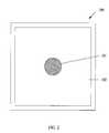
- FIG. 1is a cross-sectional view of a small vertical thin-film LED 100 .
- FIG. 2is a top view of the small vertical thin-film LED 100 of FIG. 1 .
- the vertical LED device 100has a vertical current injection configuration including a patterned n-type contact/electrode (top contact) 101 , an n-type gallium nitride based (“GaN-based”) layer 102 with a roughened surface 103 , an active region 104 , a p-type GaN-based layer 105 , a broad area reflective p-type contact/electrode 106 , a thermally and electrically conductive substrate 107 to support the device structure mechanically, and a metal bottom contact 108 .
- a n-type contact/electrode (top contact) 101a n-type gallium nitride based (“GaN-based”) layer 102 with a roughened surface 103 , an active region 104 , a p
- the n-type GaN-based layer 102is formed on a growth substrate (not shown) and the active region 104 is formed between the n-type GaN-based layer 102 and the p-type GaN-based layer 105 .
- the p-type electrode 106is directly or indirectly formed on the p-type GaN-based layer 105 .
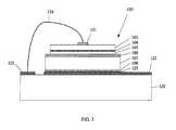
- FIG. 3is a cross-sectional view of the vertical thin-film LED 100 mounted on a sub-mount.
- the LEDsare mounted on an insulating ceramic sub-mount 120 with a p-pad 121 and an n-pad 122 .
- the bottom contact 108 (p-contact) of the LEDis attached to the p-pad 121 using conductive epoxy, solder, or eutectic 123 .
- the top contact 101 (n-contact)is connected to the n-pad 122 with bonding wires 124 .
- n-type GaN-based layer 102 and the p-type GA-based layer 105are opposite to each other, together they form a carrier injector relative to the active region 104 . Therefore, when a voltage potential is provided between the bottom contact 108 and the top contact 101 of the LED device 100 , an electrical path is formed vertically from the bottom contact 108 to the top contact 101 . Consequently, holes that are injected from the p-type GaN-based layer 105 to the active region 104 and electrons that are injected from the n-type GaN-based layer 102 to the active region 104 recombine in the active region 104 , thereby releasing energy in a form of light.
- Thermal conductivity of the low cost(the thermal conductivities of ceramic AlN or SiC are greater at 120 W/mK, but they are expensive) insulating ceramic sub-mount 120 is usually quite low (less than 40 W/mK), and the heat generated in the high power LED cannot be dissipated efficiently through the ceramic sub-mount, which limits the maximum drivability of the packaged LEDs.
- the thermal conductivity of metal sub-mountse.g., Al, Cu
- metal sub-mountsis relatively high (238 W/mK for Al, 398 W/mK for Cu) and they are ideal for minimizing the rise of LED junction temperature at high drive current condition.
- the drawback of using a metallic sub-mount for thin-film LED arraysis that the p-contacts of the thin film LEDs will all be connected via the metallic sub-mount.
- the thin-film LEDs in an arraycannot be connected in series on a metallic sub-mount unless a layer of insulating film and patterned metal traces are inserted between the LED and the metallic sub-mount to isolate the individual LED.
- the layer of insulating filmhas a low thermal conductivity and must be relatively thick, the effective thermal resistance between the junction of the LED and the metallic sub-mount is increased and the purpose of using a metallic sub-mount for packaging LEDs is compromised.
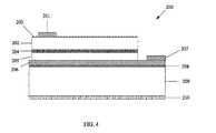
- FIG. 4is a cross-sectional view of a first configuration of a coplanar thin-film LED 200 .
- the LED device 200includes a patterned n-type contact/electrode 201 , an n-type GaN-based layer 202 with a roughened surface 203 , an active region 204 , a p-type GaN-based layer 205 , a reflective p-type contact/electrode 206 , a p-contact 207 , a conductive adhesive layer 208 , an insulating substrate 209 , and a metalized bottom surface 210 .
- the metal p-type electrode 206 and the conductive adhesive layer 208are thick enough to spread the current for the p-type GaN-based layer 205 and together may have a thickness greater than about 1 um.
- the conductive adhesive layer 208may be eutectic metal, solder metal, silver epoxy, or another type of conductive adhesive. In an LED array, it is important to be able to connect LEDs in parallel and/or in series to match the LED driver's voltage and/or current.
- the p-contact 207 and the n-contact 201are on the same side of the LED 200 (i.e., they are coplanar) and are electrically isolated from the substrate 209 .
- the substrate 209is an electrically insulated or resistive substrate (i.e., an insulator, a dielectric, and/or a substance the resists the flow of electric current) and may be formed of Al 2 O 3 , high resistivity Si, semi-insulating GaAs, or InP.
- the substrate 209may be transparent for the wavelengths between about 300 nm to 700 nm with a transmittance greater than about 50% (e.g., crystalline form of Al 2 O 3 , SiC, and AlN).
- the transmittancemay be at least 60% for blue and yellow light.
- some light raysinevitably are reflected from the silicone/air interface, reflector cup, phosphor particles and neighboring dies, and enter the transparent substrate 209 .
- the interface between 208 / 209 and 210 / 209may have reflectance greater than 60% to redirect the strayed light rays to escape the substrate 209 .
- the substrate 209may be reflective for the wavelength between about 300 nm and 700 nm with a reflectance greater than about 50% (e.g., ceramic/amorphous form of Al 2 O 3 ).
- the metalized bottom surface 210allows the LED device 200 to be attached to the metallic sub-mount.
- FIG. 5is a cross-sectional view of a plurality of the coplanar thin-film LEDs 200 of the first configuration mounted in series on a metallic sub-mount 220 .
- the LEDs 200may be mounted to the metallic sub-mount 220 with thermally conductive adhesives or eutectic solders 221 to minimize the thermal resistance between the insulating substrate 209 and the metallic sub-mount 220 .
- the LEDs 200are located such that the p and n contacts of the LEDs 200 are isolated from other devices in the array.
- the n-pad 223 and the p-pad 224are mounted to the metallic sub-mount 220 with an intervening layer of insulating film 222 to insulate the n-pad 223 and the p-pad 224 from being electrically coupled to the metallic sub-mount 220 .
- the LEDscan be connected in parallel or in series. As shown in FIG. 5 , the LEDs 200 are connected in series.
- FIG. 6is a cross-section view of a coplanar thin-film LED 300 according to a second configuration.
- the LED device 300includes a patterned n-type contact/electrode 301 , an n-type GaN-based layer 302 with a roughened surface 303 , an active region 304 , a p-type GaN-based layer 305 , a reflective p-type contact/electrode 306 , a p-contact 307 , a conductive adhesive layer 308 , an insulating dielectric film layer 309 , a substrate 310 , and a metalized bottom surface 311 .
- the metal p-type electrode 306 and the conductive adhesive layer 308are thick enough to spread the current for the p-type GaN-based layer 305 and together may have a thickness greater than about 1 um.
- an additional insulating dielectric film layer 312may be located between the substrate 310 and the metalized bottom surface 311 .
- the substrate 310may be an insulator or may be electrically conductive.
- the substrate 310may be transparent for the wavelengths between about 300 nm to 700 nm with a transmittance greater than about 50%.
- the transmittancemay be at least 60% for blue and yellow light.
- the substrate 310may be reflective for the wavelength between about 300 nm and 700 nm with a reflectance greater than about 50%.
- the insulating dielectric film layer 309insulates the substrate 310 from the p-type electrode 306 .
- the insulating dielectric film layer 309can be as thin as 0.1 um and has no impact on the thermal resistance of the LED device 300 .
- the edge of the p-type electrode 306is recessed from an edge of the chip to avoid metal debris shorting the p-contact 307 to the substrate 310 during the die singulation process.
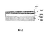
- FIGS. 7-14are cross-sectional views showing a process of manufacture of the coplanar thin-film LED of the first configuration.
- an epitaxial structure including an n-type GaN-based layer 202 , an active region 204 , and a p-type GaN-based layer 205are grown/formed on the sapphire (Al2O3) or silicon carbide (SiC) substrate 250 .
- a reflective p-type contact/electrode 206 with a capping layere.g., Au
- an insulating substrate 209 with a conductive adhesive layer 208is bonded through applied pressure to the reflective p-type electrode 206 .
- the conductive adhesive layer 208may be eutectic metal, solder metal, silver epoxy, or another type of conductive adhesive. Pressure is applied to put the two wafer surfaces 206 , 208 in intimate contact. Heat may be provided to melt the conductive adhesive layer 208 to join the two wafers 260 , 270 together.
- the growth substrate 250is removed. If the growth substrate 250 is a sapphire substrate, the growth substrate 250 may be removed through a laser lift-off (LLO) process in which a UV laser with a photon energy greater than the GaN band gap energy is applied. In an exemplary configuration, a UV laser with a wavelength of about 248 nm is used in the LLO process. If the growth substrate 250 is a SiC substrate, the growth substrate 250 may be removed through mechanical thinning and chemical etching. As shown in FIG.
- LLOlaser lift-off
- a mesa 280is formed by etching the epitaxial structure (i.e., the n-type GaN-based layer 202 , active region 204 , and the p-type GaN-based layer 205 ) to expose the reflective p-type electrode 206 .
- the epitaxial structurei.e., the n-type GaN-based layer 202 , active region 204 , and the p-type GaN-based layer 205
- a surface of the n-type GaN-based layer 202is roughened with wet chemistry efficiency to create micro-structures 203 for enhanced light extraction.
- the micro-structures 203are between about 200 nm and 400 nm in size.
- the micro-structures 203are between about 100 nm and 500 nm in size.
- the n-contact 201is formed on the n-type GaN-based layer 202 and the p-contact 207 is formed on the reflective p-type electrode 206 . If the p-type electrode 206 is not fully exposed when the epitaxial structure is etched and a thin layer of the p-Type GaN-based layer 205 remains, the p-contact 207 may be formed on the exposed p-type GaN-based layer 205 .
- the n-contact 201 and the p-contact 207are metal and may be Cr, Ti, aluminum, platinum, Au or the like.
- the substrate 209is thinned to a desired thickness and, as shown in FIG. 14 , the metalized bottom surface 210 is deposited on a bottom surface of the substrate 209 .
- FIGS. 15-23are cross-sectional views showing a process of manufacture of the coplanar thin-film LED of the second configuration.
- an epitaxial structure including an n-type GaN-based layer 302 , an active region 304 , and a p-type GA-based layer 305are grown/formed on the sapphire or silicon carbide (SiC) substrate 350 .
- a reflective p-type contact/electrode 306 with a capping layere.g., Au
- an insulating or electrically conductive substrate 310 with an insulating dielectric film layer 309 and an adhesive layer 308is bonded through applied pressure to the reflective p-type electrode 306 .
- the adhesive layer 308may be eutectic metal, solder metal, or the like. Pressure is applied to put the two wafer surfaces 306 , 308 in intimate contact. Heat may be provided to melt the adhesive layer 308 to join the two wafers 360 , 370 together.
- the growth substrate 350is removed. If the growth substrate 350 is a sapphire substrate, the growth substrate 350 may be removed through a laser lift-off (LLO) process in which a UV laser with a photon energy greater than the GaN band gap energy is applied. In an exemplary configuration, a UV laser with a wavelength of about 248 nm is used in the LLO process. If the growth substrate 350 is a SiC substrate, the growth substrate 350 may be removed through mechanical thinning and chemical etching. As shown in FIG.
- LLOlaser lift-off
- a mesa 380is formed by etching the epitaxial structure (i.e., the n-type GaN-based layer 302 , active region 304 , and the p-type GaN-based layer 305 ) to expose the reflective p-type electrode 306 .
- recesses 390are formed in the reflective p-type electrode 306 and conductive adhesive layer 308 to recess the current spreading layer ( 306 + 308 ) from the edge of the chip to avoid metal debris shoring the p-contact of the LED to the substrate 310 during the die singulation process. As shown in FIG.
- a surface of the n-type GaN-based layer 302is roughened with wet chemistry to create micro-structures 303 for enhanced light extraction efficiency.
- the micro-structures 303are between about 200 nm and 400 nm in size. In another exemplary configuration, the micro-structures 303 are between about 100 nm and 500 nm in size.
- the n-contact 301is formed on the n-type GaN-based layer 302 and the p-contact 307 is formed on the reflective p-type electrode 306 .
- the p-contact 307may be formed on the exposed p-type GaN-based layer 305 .
- the n-contact 301 and the p-contact 307are metal and may be Cr, Ti, aluminum, platinum, Au or the like.
- the substrate 310is thinned to a desired thickness and, as shown in FIG. 22 , the metalized bottom surface 311 is deposited on a bottom surface of the substrate 310 .
- an additional insulating dielectric film layer 312may be formed on the bottom surface of the substrate 310 and the metalized bottom surface 311 may be deposited on the insulating dielectric film layer 312 .
- FIG. 24is a top view showing a first example of a small coplanar thin-film LED of the first and second configurations.
- the n-contact 201 , 301is circular and is formed on the mesa 280 , 380 .
- the p-contact 207 , 307is formed at a corner of the die, adjacent to the edge of the die 400 .
- the shape of the n-contact 201 , 301is not limited to the illustrated electrode pattern and there may be more than one p-contact.
- FIG. 25is a top view showing a second example of the coplanar thin-film LED of the first and second configurations. As shown in FIG.
- the n-contact 201 , 301is formed with four fingers and a crossbar on the mesa 280 , 380 .
- the p-contacts 207 , 307are formed at corners of the die, adjacent to the edge of the die 400 .
Landscapes
- Led Devices (AREA)
- Led Device Packages (AREA)
Abstract
Description
Claims (12)
Priority Applications (15)
| Application Number | Priority Date | Filing Date | Title |
|---|---|---|---|
| US12/482,413US8207547B2 (en) | 2009-06-10 | 2009-06-10 | Thin-film LED with P and N contacts electrically isolated from the substrate |
| US12/790,597US20100314649A1 (en) | 2009-06-10 | 2010-05-28 | Thin-film led with p and n contacts electricall isolated from the substrate |
| PCT/US2010/036784WO2010144270A1 (en) | 2009-06-10 | 2010-05-30 | Thin-film led with p and n contacts electrically isolated from the substrate |
| CN201080035284.8ACN102460639B (en) | 2009-06-10 | 2010-05-30 | Thin-film LEDs with p-contacts and n-contacts electrically isolated from the substrate |
| CN201510093818.7ACN104810435A (en) | 2009-06-10 | 2010-05-30 | Thin-film LED with P and N contacts electrically isolated from the substrate |
| EP10786575.0AEP2519961B1 (en) | 2009-06-10 | 2010-05-30 | Thin-film led with p and n contacts electrically isolated from the substrate |
| KR1020127000661AKR101313973B1 (en) | 2009-06-10 | 2010-05-30 | Thin-film led with p and n contacts electrically isolated from the substrate |
| JP2012514990AJP2012529772A (en) | 2009-06-10 | 2010-05-30 | Thin film LED with p-type and n-type contacts electrically isolated from the substrate |
| TW104108910ATW201526280A (en) | 2009-06-10 | 2010-06-04 | Light-emitting diode and light-emitting device |
| TW099118138ATWI482309B (en) | 2009-06-10 | 2010-06-04 | Thin film light-emitting diode with P contact and N contact electrically insulated from the substrate |
| US12/835,632US8536601B2 (en) | 2009-06-10 | 2010-07-13 | Thin-film LED with P and N contacts electrically isolated from the substrate |
| US13/532,749US8546832B2 (en) | 2009-06-10 | 2012-06-25 | Thin-film LED with p and n contacts electrically isolated from the substrate |
| US13/892,188US8871539B2 (en) | 2009-06-10 | 2013-05-10 | Thin-film LED with P and N contacts electrically isolated from the substrate |
| US13/965,799US9142742B2 (en) | 2009-06-10 | 2013-08-13 | Thin-film LED with P and N contacts electrically isolated from the substrate |
| JP2014044677AJP6092798B2 (en) | 2009-06-10 | 2014-03-07 | Manufacturing method of semiconductor device |
Applications Claiming Priority (1)
| Application Number | Priority Date | Filing Date | Title |
|---|---|---|---|
| US12/482,413US8207547B2 (en) | 2009-06-10 | 2009-06-10 | Thin-film LED with P and N contacts electrically isolated from the substrate |
Related Parent Applications (3)
| Application Number | Title | Priority Date | Filing Date |
|---|---|---|---|
| US12/790,597DivisionUS20100314649A1 (en) | 2009-06-10 | 2010-05-28 | Thin-film led with p and n contacts electricall isolated from the substrate |
| US12/835,632DivisionUS8536601B2 (en) | 2009-06-10 | 2010-07-13 | Thin-film LED with P and N contacts electrically isolated from the substrate |
| US13/532,749ContinuationUS8546832B2 (en) | 2009-06-10 | 2012-06-25 | Thin-film LED with p and n contacts electrically isolated from the substrate |
Related Child Applications (3)
| Application Number | Title | Priority Date | Filing Date |
|---|---|---|---|
| US12/790,597DivisionUS20100314649A1 (en) | 2009-06-10 | 2010-05-28 | Thin-film led with p and n contacts electricall isolated from the substrate |
| US12/835,632DivisionUS8536601B2 (en) | 2009-06-10 | 2010-07-13 | Thin-film LED with P and N contacts electrically isolated from the substrate |
| US13/532,749ContinuationUS8546832B2 (en) | 2009-06-10 | 2012-06-25 | Thin-film LED with p and n contacts electrically isolated from the substrate |
Publications (2)
| Publication Number | Publication Date |
|---|---|
| US20100314643A1 US20100314643A1 (en) | 2010-12-16 |
| US8207547B2true US8207547B2 (en) | 2012-06-26 |
Family
ID=43305661
Family Applications (6)
| Application Number | Title | Priority Date | Filing Date |
|---|---|---|---|
| US12/482,413ActiveUS8207547B2 (en) | 2009-06-10 | 2009-06-10 | Thin-film LED with P and N contacts electrically isolated from the substrate |
| US12/790,597AbandonedUS20100314649A1 (en) | 2009-06-10 | 2010-05-28 | Thin-film led with p and n contacts electricall isolated from the substrate |
| US12/835,632Active2029-08-02US8536601B2 (en) | 2009-06-10 | 2010-07-13 | Thin-film LED with P and N contacts electrically isolated from the substrate |
| US13/532,749ActiveUS8546832B2 (en) | 2009-06-10 | 2012-06-25 | Thin-film LED with p and n contacts electrically isolated from the substrate |
| US13/892,188Active2029-06-17US8871539B2 (en) | 2009-06-10 | 2013-05-10 | Thin-film LED with P and N contacts electrically isolated from the substrate |
| US13/965,799ActiveUS9142742B2 (en) | 2009-06-10 | 2013-08-13 | Thin-film LED with P and N contacts electrically isolated from the substrate |
Family Applications After (5)
| Application Number | Title | Priority Date | Filing Date |
|---|---|---|---|
| US12/790,597AbandonedUS20100314649A1 (en) | 2009-06-10 | 2010-05-28 | Thin-film led with p and n contacts electricall isolated from the substrate |
| US12/835,632Active2029-08-02US8536601B2 (en) | 2009-06-10 | 2010-07-13 | Thin-film LED with P and N contacts electrically isolated from the substrate |
| US13/532,749ActiveUS8546832B2 (en) | 2009-06-10 | 2012-06-25 | Thin-film LED with p and n contacts electrically isolated from the substrate |
| US13/892,188Active2029-06-17US8871539B2 (en) | 2009-06-10 | 2013-05-10 | Thin-film LED with P and N contacts electrically isolated from the substrate |
| US13/965,799ActiveUS9142742B2 (en) | 2009-06-10 | 2013-08-13 | Thin-film LED with P and N contacts electrically isolated from the substrate |
Country Status (7)
| Country | Link |
|---|---|
| US (6) | US8207547B2 (en) |
| EP (1) | EP2519961B1 (en) |
| JP (2) | JP2012529772A (en) |
| KR (1) | KR101313973B1 (en) |
| CN (2) | CN102460639B (en) |
| TW (2) | TW201526280A (en) |
| WO (1) | WO2010144270A1 (en) |
Cited By (79)
| Publication number | Priority date | Publication date | Assignee | Title |
|---|---|---|---|---|
| US20130328093A1 (en)* | 2009-06-10 | 2013-12-12 | Toshiba Techno Center Inc. | Thin-film led with p and n contacts electrically isolated from the substrate |
| US20140217356A1 (en)* | 2013-02-05 | 2014-08-07 | International Business Machines Corporation | Thin film wafer transfer and structure for electronic devices |
| US9358775B2 (en) | 2014-07-20 | 2016-06-07 | X-Celeprint Limited | Apparatus and methods for micro-transfer-printing |
| US9368683B1 (en) | 2015-05-15 | 2016-06-14 | X-Celeprint Limited | Printable inorganic semiconductor method |
| US9437782B2 (en) | 2014-06-18 | 2016-09-06 | X-Celeprint Limited | Micro assembled LED displays and lighting elements |
| US9468050B1 (en) | 2014-09-25 | 2016-10-11 | X-Celeprint Limited | Self-compensating circuit for faulty display pixels |
| US9537069B1 (en) | 2014-09-25 | 2017-01-03 | X-Celeprint Limited | Inorganic light-emitting diode with encapsulating reflector |
| US9601356B2 (en) | 2014-06-18 | 2017-03-21 | X-Celeprint Limited | Systems and methods for controlling release of transferable semiconductor structures |
| US9640108B2 (en) | 2015-08-25 | 2017-05-02 | X-Celeprint Limited | Bit-plane pulse width modulated digital display system |
| US9704821B2 (en) | 2015-08-11 | 2017-07-11 | X-Celeprint Limited | Stamp with structured posts |
| US9716082B2 (en) | 2014-08-26 | 2017-07-25 | X-Celeprint Limited | Micro assembled hybrid displays and lighting elements |
| US9741785B2 (en) | 2014-09-25 | 2017-08-22 | X-Celeprint Limited | Display tile structure and tiled display |
| US9761754B2 (en) | 2014-06-18 | 2017-09-12 | X-Celeprint Limited | Systems and methods for preparing GaN and related materials for micro assembly |
| US9786646B2 (en) | 2015-12-23 | 2017-10-10 | X-Celeprint Limited | Matrix addressed device repair |
| US9799261B2 (en) | 2014-09-25 | 2017-10-24 | X-Celeprint Limited | Self-compensating circuit for faulty display pixels |
| US9818725B2 (en) | 2015-06-01 | 2017-11-14 | X-Celeprint Limited | Inorganic-light-emitter display with integrated black matrix |
| US9865600B2 (en) | 2014-06-18 | 2018-01-09 | X-Celeprint Limited | Printed capacitors |
| US9871345B2 (en) | 2015-06-09 | 2018-01-16 | X-Celeprint Limited | Crystalline color-conversion device |
| US9923133B2 (en) | 2010-08-26 | 2018-03-20 | X-Celeprint Limited | Structures and methods for testing printable integrated circuits |
| US9929053B2 (en) | 2014-06-18 | 2018-03-27 | X-Celeprint Limited | Systems and methods for controlling release of transferable semiconductor structures |
| US9928771B2 (en) | 2015-12-24 | 2018-03-27 | X-Celeprint Limited | Distributed pulse width modulation control |
| US9930277B2 (en) | 2015-12-23 | 2018-03-27 | X-Celeprint Limited | Serial row-select matrix-addressed system |
| US9980341B2 (en) | 2016-09-22 | 2018-05-22 | X-Celeprint Limited | Multi-LED components |
| US9991163B2 (en) | 2014-09-25 | 2018-06-05 | X-Celeprint Limited | Small-aperture-ratio display with electrical component |
| US9997501B2 (en) | 2016-06-01 | 2018-06-12 | X-Celeprint Limited | Micro-transfer-printed light-emitting diode device |
| US9997102B2 (en) | 2016-04-19 | 2018-06-12 | X-Celeprint Limited | Wirelessly powered display and system |
| US10008483B2 (en) | 2016-04-05 | 2018-06-26 | X-Celeprint Limited | Micro-transfer printed LED and color filter structure |
| US10008465B2 (en) | 2011-06-08 | 2018-06-26 | X-Celeprint Limited | Methods for surface attachment of flipped active components |
| US10050351B2 (en) | 2014-06-18 | 2018-08-14 | X-Celeprint Limited | Multilayer printed capacitors |
| US10066819B2 (en) | 2015-12-09 | 2018-09-04 | X-Celeprint Limited | Micro-light-emitting diode backlight system |
| US10091446B2 (en) | 2015-12-23 | 2018-10-02 | X-Celeprint Limited | Active-matrix displays with common pixel control |
| US10102794B2 (en) | 2015-06-09 | 2018-10-16 | X-Celeprint Limited | Distributed charge-pump power-supply system |
| US10103069B2 (en) | 2016-04-01 | 2018-10-16 | X-Celeprint Limited | Pressure-activated electrical interconnection by micro-transfer printing |
| US10109753B2 (en) | 2016-02-19 | 2018-10-23 | X-Celeprint Limited | Compound micro-transfer-printed optical filter device |
| US10133426B2 (en) | 2015-06-18 | 2018-11-20 | X-Celeprint Limited | Display with micro-LED front light |
| US10153257B2 (en) | 2016-03-03 | 2018-12-11 | X-Celeprint Limited | Micro-printed display |
| US10153256B2 (en) | 2016-03-03 | 2018-12-11 | X-Celeprint Limited | Micro-transfer printable electronic component |
| US10150326B2 (en) | 2016-02-29 | 2018-12-11 | X-Celeprint Limited | Hybrid document with variable state |
| US10150325B2 (en) | 2016-02-29 | 2018-12-11 | X-Celeprint Limited | Hybrid banknote with electronic indicia |
| US10157880B2 (en) | 2016-10-03 | 2018-12-18 | X-Celeprint Limited | Micro-transfer printing with volatile adhesive layer |
| US10181483B2 (en) | 2010-03-29 | 2019-01-15 | X-Celeprint Limited | Laser assisted transfer welding process |
| US10189243B2 (en) | 2011-09-20 | 2019-01-29 | X-Celeprint Limited | Printing transferable components using microstructured elastomeric surfaces with pressure modulated reversible adhesion |
| US10193025B2 (en) | 2016-02-29 | 2019-01-29 | X-Celeprint Limited | Inorganic LED pixel structure |
| US10200013B2 (en) | 2016-02-18 | 2019-02-05 | X-Celeprint Limited | Micro-transfer-printed acoustic wave filter device |
| US10199546B2 (en) | 2016-04-05 | 2019-02-05 | X-Celeprint Limited | Color-filter device |
| US10198890B2 (en) | 2016-04-19 | 2019-02-05 | X-Celeprint Limited | Hybrid banknote with electronic indicia using near-field-communications |
| US10217730B2 (en) | 2016-02-25 | 2019-02-26 | X-Celeprint Limited | Efficiently micro-transfer printing micro-scale devices onto large-format substrates |
| US10224231B2 (en) | 2016-11-15 | 2019-03-05 | X-Celeprint Limited | Micro-transfer-printable flip-chip structures and methods |
| US10222698B2 (en) | 2016-07-28 | 2019-03-05 | X-Celeprint Limited | Chiplets with wicking posts |
| US10230048B2 (en) | 2015-09-29 | 2019-03-12 | X-Celeprint Limited | OLEDs for micro transfer printing |
| US10255834B2 (en) | 2015-07-23 | 2019-04-09 | X-Celeprint Limited | Parallel redundant chiplet system for controlling display pixels |
| US10297502B2 (en) | 2016-12-19 | 2019-05-21 | X-Celeprint Limited | Isolation structure for micro-transfer-printable devices |
| US10347168B2 (en) | 2016-11-10 | 2019-07-09 | X-Celeprint Limited | Spatially dithered high-resolution |
| US10360846B2 (en) | 2016-05-10 | 2019-07-23 | X-Celeprint Limited | Distributed pulse-width modulation system with multi-bit digital storage and output device |
| US10361677B2 (en) | 2016-02-18 | 2019-07-23 | X-Celeprint Limited | Transverse bulk acoustic wave filter |
| US10380930B2 (en) | 2015-08-24 | 2019-08-13 | X-Celeprint Limited | Heterogeneous light emitter display system |
| US10395966B2 (en) | 2016-11-15 | 2019-08-27 | X-Celeprint Limited | Micro-transfer-printable flip-chip structures and methods |
| US10396137B2 (en) | 2017-03-10 | 2019-08-27 | X-Celeprint Limited | Testing transfer-print micro-devices on wafer |
| US10418331B2 (en) | 2010-11-23 | 2019-09-17 | X-Celeprint Limited | Interconnection structures and methods for transfer-printed integrated circuit elements with improved interconnection alignment tolerance |
| US10438859B2 (en) | 2016-12-19 | 2019-10-08 | X-Celeprint Limited | Transfer printed device repair |
| US10453826B2 (en) | 2016-06-03 | 2019-10-22 | X-Celeprint Limited | Voltage-balanced serial iLED pixel and display |
| US10468363B2 (en) | 2015-08-10 | 2019-11-05 | X-Celeprint Limited | Chiplets with connection posts |
| US10505079B2 (en) | 2018-05-09 | 2019-12-10 | X-Celeprint Limited | Flexible devices and methods using laser lift-off |
| US10600671B2 (en) | 2016-11-15 | 2020-03-24 | X-Celeprint Limited | Micro-transfer-printable flip-chip structures and methods |
| US10622700B2 (en) | 2016-05-18 | 2020-04-14 | X-Celeprint Limited | Antenna with micro-transfer-printed circuit element |
| US10748793B1 (en) | 2019-02-13 | 2020-08-18 | X Display Company Technology Limited | Printing component arrays with different orientations |
| US10782002B2 (en) | 2016-10-28 | 2020-09-22 | X Display Company Technology Limited | LED optical components |
| US10832935B2 (en) | 2017-08-14 | 2020-11-10 | X Display Company Technology Limited | Multi-level micro-device tethers |
| US10832609B2 (en) | 2017-01-10 | 2020-11-10 | X Display Company Technology Limited | Digital-drive pulse-width-modulated output system |
| US10832934B2 (en) | 2018-06-14 | 2020-11-10 | X Display Company Technology Limited | Multi-layer tethers for micro-transfer printing |
| US10944034B2 (en) | 2018-08-24 | 2021-03-09 | Lextar Electronics Corporation | Light emitting diode structure |
| US11024608B2 (en) | 2017-03-28 | 2021-06-01 | X Display Company Technology Limited | Structures and methods for electrical connection of micro-devices and substrates |
| US11038088B2 (en) | 2019-10-14 | 2021-06-15 | Lextar Electronics Corporation | Light emitting diode package |
| US11061276B2 (en) | 2015-06-18 | 2021-07-13 | X Display Company Technology Limited | Laser array display |
| US11064609B2 (en) | 2016-08-04 | 2021-07-13 | X Display Company Technology Limited | Printable 3D electronic structure |
| US11137641B2 (en) | 2016-06-10 | 2021-10-05 | X Display Company Technology Limited | LED structure with polarized light emission |
| US20210351230A1 (en) | 2017-11-27 | 2021-11-11 | Seoul Viosys Co., Ltd. | Light emitting diode (led) stack for a display |
| US20220130898A1 (en) | 2017-11-27 | 2022-04-28 | Seoul Viosys Co., Ltd. | Light emitting device having commonly connected led sub-units |
| US12107081B2 (en) | 2017-12-20 | 2024-10-01 | Seoul Viosys Co., Ltd. | LED unit for display and display apparatus having the same |
Families Citing this family (33)
| Publication number | Priority date | Publication date | Assignee | Title |
|---|---|---|---|---|
| US8604500B2 (en)* | 2010-03-17 | 2013-12-10 | Lg Innotek Co., Ltd. | Light emitting device and light emitting device package |
| US8993993B2 (en)* | 2010-05-11 | 2015-03-31 | Samsung Electronics Co., Ltd. | Semiconductor light emitting device and method for fabricating the same |
| DE102010026344A1 (en)* | 2010-07-07 | 2012-01-12 | Osram Opto Semiconductors Gmbh | led |
| EP2447595B1 (en)* | 2010-10-27 | 2017-08-02 | LG Innotek Co., Ltd. | Light emitting module |
| JP2012124473A (en)* | 2010-11-15 | 2012-06-28 | Ngk Insulators Ltd | Composite substrate and method for manufacturing the same |
| KR101035998B1 (en)* | 2010-11-18 | 2011-05-23 | 한빔 주식회사 | Vertical LED Manufacturing Method |
| US8476649B2 (en)* | 2010-12-16 | 2013-07-02 | Micron Technology, Inc. | Solid state lighting devices with accessible electrodes and methods of manufacturing |
| JP5806608B2 (en)* | 2011-12-12 | 2015-11-10 | 株式会社東芝 | Semiconductor light emitting device |
| US8598611B2 (en) | 2012-01-09 | 2013-12-03 | Micron Technology, Inc. | Vertical solid-state transducers and solid-state transducer arrays having backside terminals and associated systems and methods |
| WO2013119868A1 (en)* | 2012-02-07 | 2013-08-15 | Ritedia Corporation | LIGHT TRANSMITTIVE AlN LAYERS AND ASSOCIATED DEVICES AND METHODS |
| CN103474545B (en)* | 2012-06-07 | 2016-06-08 | 清华大学 | Light emitting diode |
| CN103474549B (en)* | 2012-06-07 | 2016-12-14 | 清华大学 | Semiconductor structure |
| WO2014047724A1 (en) | 2012-09-26 | 2014-04-03 | Ledtech International Inc. | Multilayer optical interference filter |
| JP2014154693A (en)* | 2013-02-08 | 2014-08-25 | Toyoda Gosei Co Ltd | Group iii nitride semiconductor light-emitting element and manufacturing method of the same |
| TWI613842B (en)* | 2014-04-08 | 2018-02-01 | 晶元光電股份有限公司 | Illuminating device |
| DE102014105999A1 (en)* | 2014-04-29 | 2015-10-29 | Osram Opto Semiconductors Gmbh | Optoelectronic semiconductor chip and method for producing an optoelectronic semiconductor chip |
| US10211185B2 (en)* | 2014-10-31 | 2019-02-19 | Bridgelux Inc. | High efficiency chip-on-board light-emitting diode |
| JP2016207739A (en)* | 2015-04-17 | 2016-12-08 | 株式会社東芝 | Semiconductor light emitting device and manufacturing method of the same |
| TWI572058B (en) | 2015-09-04 | 2017-02-21 | 錼創科技股份有限公司 | Light-emitting element manufacturing method |
| KR20180132684A (en)* | 2016-03-12 | 2018-12-12 | 닝보 써니 오포테크 코., 엘티디. | Camera module, its photosensitive part and method of manufacturing the same |
| TWI730096B (en) | 2016-05-20 | 2021-06-11 | 荷蘭商露明控股公司 | Light emitting devices and methods for growing the same |
| CN108305918B (en)* | 2017-01-12 | 2019-07-16 | 中国科学院苏州纳米技术与纳米仿生研究所 | Nitride semiconductor light-emitting device and method of making the same |
| TWI679762B (en)* | 2018-03-06 | 2019-12-11 | 友達光電股份有限公司 | Display device and manufacturing method thereof |
| DE102018123931A1 (en)* | 2018-09-27 | 2020-04-02 | Osram Opto Semiconductors Gmbh | Optoelectronic semiconductor component with sapphire carrier and method for producing the optoelectronic semiconductor component |
| WO2020142976A1 (en)* | 2019-01-10 | 2020-07-16 | Shenzhen Xpectvision Technology Co., Ltd. | X-ray detectors based on an epitaxial layer and methods of making |
| WO2020155176A1 (en)* | 2019-02-03 | 2020-08-06 | 泉州三安半导体科技有限公司 | Light-emitting apparatus |
| US10930814B1 (en) | 2019-09-11 | 2021-02-23 | Jade Bird Display (shanghai) Limited | Method of manufacturing multi-color light emitting pixel unit |
| US12426428B2 (en) | 2019-09-11 | 2025-09-23 | Jade Bird Display (shanghai) Limited | Multi-color LED pixel unit and micro-LED display panel |
| TWI766196B (en)* | 2019-10-16 | 2022-06-01 | 日商牛尾電機股份有限公司 | semiconductor light emitting device |
| WO2021202075A1 (en) | 2020-04-03 | 2021-10-07 | Cree, Inc. | Rf amplifier package |
| US12074123B2 (en) | 2020-04-03 | 2024-08-27 | Macom Technology Solutions Holdings, Inc. | Multi level radio frequency (RF) integrated circuit components including passive devices |
| US11863130B2 (en) | 2020-04-03 | 2024-01-02 | Wolfspeed, Inc. | Group III nitride-based radio frequency transistor amplifiers having source, gate and/or drain conductive vias |
| CN114447176B (en)* | 2022-01-28 | 2024-09-27 | 上海芯元基半导体科技有限公司 | Thin-film LED chip with vertical structure, micro LED array and preparation method thereof |
Citations (9)
| Publication number | Priority date | Publication date | Assignee | Title |
|---|---|---|---|---|
| US3860424A (en)* | 1971-12-30 | 1975-01-14 | Bell Telephone Labor Inc | Led display |
| US20020175352A1 (en)* | 2001-07-10 | 2002-11-28 | Cao Group, Inc. | Light for use in activating light-activated materials, the light having a plurality of light emitting single chip arrays |
| US20030010975A1 (en)* | 2001-07-05 | 2003-01-16 | Gelcore Llc | GaN LED with solderable backside metal |
| US6803122B2 (en) | 2000-12-12 | 2004-10-12 | Tdk Corporation | EL device |
| US20050224822A1 (en)* | 2003-07-04 | 2005-10-13 | Wen-Huang Liu | Light-emitting diode array having an adhesive layer |
| CN1874012A (en)* | 2005-06-03 | 2006-12-06 | 北京大学 | High-luminance chip of luminescent tube in GaN base, and preparation method |
| US7242031B2 (en) | 2004-03-02 | 2007-07-10 | Kabushiki Kaisha Toshiba | Semiconductor light emitting apparatus and its manufacturing method |
| US20090134420A1 (en) | 2003-12-24 | 2009-05-28 | Panasonic Corporation | Semiconductor light emitting device, lighting module, lighting apparatus, display element, and manufacturing method for semiconductor light emitting device |
| US7816703B2 (en)* | 2007-12-14 | 2010-10-19 | Delta Electronics, Inc. | Light-emitting diode device and manufacturing method thereof |
Family Cites Families (135)
| Publication number | Priority date | Publication date | Assignee | Title |
|---|---|---|---|---|
| JPH0363756A (en) | 1989-07-31 | 1991-03-19 | Fuji Xerox Co Ltd | Document editor |
| JP2706522B2 (en) | 1989-07-31 | 1998-01-28 | 松下電器産業株式会社 | Document creation device |
| JP2708574B2 (en) | 1989-10-20 | 1998-02-04 | 新日本製鐵株式会社 | Manufacturing method of bonding wire for semiconductor |
| US5048721A (en) | 1989-11-17 | 1991-09-17 | Union Carbide Industrial Gases Technology Corporation | Method for enhancing the mixture of gases within a cylinder |
| JP2759836B2 (en) | 1990-01-30 | 1998-05-28 | 富士写真光機株式会社 | Camera self-shooting method |
| JPH03250438A (en) | 1990-02-27 | 1991-11-08 | Sanyo Electric Co Ltd | Optical recording medium |
| JP2948889B2 (en) | 1990-09-05 | 1999-09-13 | 光洋精工株式会社 | Rack and pinion steering system |
| JPH04118370A (en) | 1990-09-07 | 1992-04-20 | Mazda Motor Corp | Hydraulic driver for rear-wheel steering system |
| JP2721047B2 (en)* | 1991-01-14 | 1998-03-04 | 三菱電機株式会社 | Submount for semiconductor device and semiconductor optical device module |
| US5306662A (en)* | 1991-11-08 | 1994-04-26 | Nichia Chemical Industries, Ltd. | Method of manufacturing P-type compound semiconductor |
| JP2917742B2 (en) | 1992-07-07 | 1999-07-12 | 日亜化学工業株式会社 | Gallium nitride based compound semiconductor light emitting device and method of manufacturing the same |
| EP0579897B1 (en)* | 1992-07-23 | 2003-10-15 | Toyoda Gosei Co., Ltd. | Light-emitting device of gallium nitride compound semiconductor |
| JP2626431B2 (en) | 1992-10-29 | 1997-07-02 | 豊田合成株式会社 | Nitrogen-3 group element compound semiconductor light emitting device |
| JP2681733B2 (en) | 1992-10-29 | 1997-11-26 | 豊田合成株式会社 | Nitrogen-3 group element compound semiconductor light emitting device |
| US5578839A (en)* | 1992-11-20 | 1996-11-26 | Nichia Chemical Industries, Ltd. | Light-emitting gallium nitride-based compound semiconductor device |
| JP2827794B2 (en) | 1993-02-05 | 1998-11-25 | 日亜化学工業株式会社 | Method for growing p-type gallium nitride |
| JP2778405B2 (en) | 1993-03-12 | 1998-07-23 | 日亜化学工業株式会社 | Gallium nitride based compound semiconductor light emitting device |
| JP2803741B2 (en) | 1993-03-19 | 1998-09-24 | 日亜化学工業株式会社 | Gallium nitride based compound semiconductor electrode forming method |
| EP0622858B2 (en)* | 1993-04-28 | 2004-09-29 | Nichia Corporation | Gallium nitride-based III-V group compound semiconductor device and method of producing the same |
| JP2785254B2 (en) | 1993-06-28 | 1998-08-13 | 日亜化学工業株式会社 | Gallium nitride based compound semiconductor light emitting device |
| US6005258A (en)* | 1994-03-22 | 1999-12-21 | Toyoda Gosei Co., Ltd. | Light-emitting semiconductor device using group III Nitrogen compound having emission layer doped with donor and acceptor impurities |
| JP2956489B2 (en) | 1994-06-24 | 1999-10-04 | 日亜化学工業株式会社 | Crystal growth method of gallium nitride based compound semiconductor |
| JP2666237B2 (en) | 1994-09-20 | 1997-10-22 | 豊田合成株式会社 | Group III nitride semiconductor light emitting device |
| JP3548442B2 (en) | 1994-09-22 | 2004-07-28 | 日亜化学工業株式会社 | Gallium nitride based compound semiconductor light emitting device |
| JP3646649B2 (en) | 1994-09-22 | 2005-05-11 | 日亜化学工業株式会社 | Gallium nitride compound semiconductor light emitting device |
| US5777350A (en)* | 1994-12-02 | 1998-07-07 | Nichia Chemical Industries, Ltd. | Nitride semiconductor light-emitting device |
| JP2735057B2 (en) | 1994-12-22 | 1998-04-02 | 日亜化学工業株式会社 | Nitride semiconductor light emitting device |
| JP2890396B2 (en) | 1995-03-27 | 1999-05-10 | 日亜化学工業株式会社 | Nitride semiconductor light emitting device |
| JP3250438B2 (en) | 1995-03-29 | 2002-01-28 | 日亜化学工業株式会社 | Nitride semiconductor light emitting device |
| JP3890930B2 (en) | 1995-03-29 | 2007-03-07 | 日亜化学工業株式会社 | Nitride semiconductor light emitting device |
| JP3511970B2 (en) | 1995-06-15 | 2004-03-29 | 日亜化学工業株式会社 | Nitride semiconductor light emitting device |
| JP3135041B2 (en) | 1995-09-29 | 2001-02-13 | 日亜化学工業株式会社 | Nitride semiconductor light emitting device |
| US5959307A (en)* | 1995-11-06 | 1999-09-28 | Nichia Chemical Industries Ltd. | Nitride semiconductor device |
| JPH09298313A (en)* | 1996-04-30 | 1997-11-18 | Rohm Co Ltd | Semiconductor light emitting element and manufacture thereof |
| JP3209096B2 (en)* | 1996-05-21 | 2001-09-17 | 豊田合成株式会社 | Group III nitride compound semiconductor light emitting device |
| JP3304787B2 (en)* | 1996-09-08 | 2002-07-22 | 豊田合成株式会社 | Semiconductor light emitting device and method of manufacturing the same |
| JP3780887B2 (en) | 1996-09-08 | 2006-05-31 | 豊田合成株式会社 | Semiconductor light emitting device and manufacturing method thereof |
| JPH10154670A (en)* | 1996-11-26 | 1998-06-09 | Toshiba Corp | Method for manufacturing semiconductor device |
| JP3344257B2 (en) | 1997-01-17 | 2002-11-11 | 豊田合成株式会社 | Gallium nitride based compound semiconductor and device manufacturing method |
| JP3374737B2 (en) | 1997-01-09 | 2003-02-10 | 日亜化学工業株式会社 | Nitride semiconductor device |
| JP3223832B2 (en) | 1997-02-24 | 2001-10-29 | 日亜化学工業株式会社 | Nitride semiconductor device and semiconductor laser diode |
| JP3506874B2 (en) | 1997-03-24 | 2004-03-15 | 豊田合成株式会社 | Nitrogen-3 group element compound semiconductor light emitting device |
| JP3795624B2 (en) | 1997-03-31 | 2006-07-12 | 豊田合成株式会社 | Nitrogen-3 group element compound semiconductor light emitting device |
| JP3654738B2 (en) | 1997-04-07 | 2005-06-02 | 豊田合成株式会社 | Group 3 nitride semiconductor light emitting device |
| US6784463B2 (en)* | 1997-06-03 | 2004-08-31 | Lumileds Lighting U.S., Llc | III-Phospide and III-Arsenide flip chip light-emitting devices |
| JP3314666B2 (en) | 1997-06-09 | 2002-08-12 | 日亜化学工業株式会社 | Nitride semiconductor device |
| JP4118370B2 (en) | 1997-12-15 | 2008-07-16 | フィリップス ルミレッズ ライティング カンパニー リミテッド ライアビリティ カンパニー | Nitride semiconductor light-emitting device having reflective p-electrode, method for manufacturing the same, and semiconductor optoelectronic device |
| EP1928034A3 (en)* | 1997-12-15 | 2008-06-18 | Philips Lumileds Lighting Company LLC | Light emitting device |
| JP4118371B2 (en) | 1997-12-15 | 2008-07-16 | フィリップス ルミレッズ ライティング カンパニー リミテッド ライアビリティ カンパニー | Nitride semiconductor light emitting device having silver as electrode, method for manufacturing the same, and semiconductor optoelectronic device |
| JP3622562B2 (en) | 1998-03-12 | 2005-02-23 | 日亜化学工業株式会社 | Nitride semiconductor light emitting diode |
| EP2273571A3 (en)* | 1998-03-12 | 2012-06-27 | Nichia Corporation | A nitride semiconductor device |
| JP4629178B2 (en) | 1998-10-06 | 2011-02-09 | 日亜化学工業株式会社 | Nitride semiconductor device |
| JP3063756B1 (en) | 1998-10-06 | 2000-07-12 | 日亜化学工業株式会社 | Nitride semiconductor device |
| JP3063757B1 (en) | 1998-11-17 | 2000-07-12 | 日亜化学工業株式会社 | Nitride semiconductor device |
| JP3424629B2 (en) | 1998-12-08 | 2003-07-07 | 日亜化学工業株式会社 | Nitride semiconductor device |
| JP3427265B2 (en) | 1998-12-08 | 2003-07-14 | 日亜化学工業株式会社 | Nitride semiconductor device |
| US20010042866A1 (en) | 1999-02-05 | 2001-11-22 | Carrie Carter Coman | Inxalygazn optical emitters fabricated via substrate removal |
| US6838705B1 (en)* | 1999-03-29 | 2005-01-04 | Nichia Corporation | Nitride semiconductor device |
| JP3551101B2 (en) | 1999-03-29 | 2004-08-04 | 日亜化学工業株式会社 | Nitride semiconductor device |
| DE19955747A1 (en)* | 1999-11-19 | 2001-05-23 | Osram Opto Semiconductors Gmbh | Optical semiconductor device with multiple quantum well structure, e.g. LED, has alternate well layers and barrier layers forming super-lattices |
| KR100700993B1 (en)* | 1999-12-03 | 2007-03-30 | 크리, 인코포레이티드 | Light emitting diode having improved light extraction structure and manufacturing method thereof |
| US6277665B1 (en)* | 2000-01-10 | 2001-08-21 | United Epitaxy Company, Ltd. | Fabrication process of semiconductor light-emitting device with enhanced external quantum efficiency |
| TWI289944B (en)* | 2000-05-26 | 2007-11-11 | Osram Opto Semiconductors Gmbh | Light-emitting-diode-element with a light-emitting-diode-chip |
| US6586762B2 (en)* | 2000-07-07 | 2003-07-01 | Nichia Corporation | Nitride semiconductor device with improved lifetime and high output power |
| JP3786114B2 (en) | 2000-11-21 | 2006-06-14 | 日亜化学工業株式会社 | Nitride semiconductor device |
| US6677059B2 (en) | 2000-12-12 | 2004-01-13 | Tdk Corporation | EL device and making method |
| US6906352B2 (en)* | 2001-01-16 | 2005-06-14 | Cree, Inc. | Group III nitride LED with undoped cladding layer and multiple quantum well |
| JP2002222997A (en) | 2001-01-25 | 2002-08-09 | Seiwa Electric Mfg Co Ltd | Surface mounting light emitting diode and method for manufacturing it |
| US6765232B2 (en)* | 2001-03-27 | 2004-07-20 | Ricoh Company, Ltd. | Semiconductor light-emitting device, surface-emission laser diode, and production apparatus thereof, production method, optical module and optical telecommunication system |
| US6630689B2 (en)* | 2001-05-09 | 2003-10-07 | Lumileds Lighting, U.S. Llc | Semiconductor LED flip-chip with high reflectivity dielectric coating on the mesa |
| US6958497B2 (en)* | 2001-05-30 | 2005-10-25 | Cree, Inc. | Group III nitride based light emitting diode structures with a quantum well and superlattice, group III nitride based quantum well structures and group III nitride based superlattice structures |
| US6488767B1 (en)* | 2001-06-08 | 2002-12-03 | Advanced Technology Materials, Inc. | High surface quality GaN wafer and method of fabricating same |
| JP3821128B2 (en)* | 2001-07-12 | 2006-09-13 | 日亜化学工業株式会社 | Semiconductor element |
| JPWO2003034508A1 (en)* | 2001-10-12 | 2005-02-03 | 日亜化学工業株式会社 | Light emitting device and manufacturing method thereof |
| WO2003065464A1 (en)* | 2002-01-28 | 2003-08-07 | Nichia Corporation | Nitride semiconductor device having support substrate and its manufacturing method |
| JP3982284B2 (en)* | 2002-03-06 | 2007-09-26 | 住友電気工業株式会社 | Submount and semiconductor device |
| KR101030068B1 (en)* | 2002-07-08 | 2011-04-19 | 니치아 카가쿠 고교 가부시키가이샤 | Nitride semiconductor device manufacturing method and nitride semiconductor device |
| TW567618B (en)* | 2002-07-15 | 2003-12-21 | Epistar Corp | Light emitting diode with adhesive reflection layer and manufacturing method thereof |
| DE10245628A1 (en)* | 2002-09-30 | 2004-04-15 | Osram Opto Semiconductors Gmbh | Light-emitting semiconductor chip includes mirror layer with planar reflection surfaces inclined at acute angle with respect to main plane of beam production region |
| FR2846572B1 (en)* | 2002-11-05 | 2004-12-31 | Centre Nat Rech Scient | DISSYMMETRIC PARTICLES OF NANOMETRIC OR MESOSCOPIC SIZE, AND PROCESS FOR THEIR PREPARATION |
| JP4050160B2 (en) | 2003-02-04 | 2008-02-20 | 株式会社東芝 | Semiconductor module, semiconductor module assembly, main circuit component and power conversion circuit |
| US7528421B2 (en)* | 2003-05-05 | 2009-05-05 | Lamina Lighting, Inc. | Surface mountable light emitting diode assemblies packaged for high temperature operation |
| TW200509408A (en)* | 2003-08-20 | 2005-03-01 | Epistar Corp | Nitride light-emitting device with high light-emitting efficiency |
| JP2005072148A (en)* | 2003-08-21 | 2005-03-17 | Mitsubishi Cable Ind Ltd | Nitride semiconductor device |
| EP2320482B1 (en)* | 2003-12-09 | 2016-11-16 | The Regents of The University of California | Highly efficient gallium nitride based light emitting diodes via surface roughening |
| JP3928621B2 (en) | 2004-01-19 | 2007-06-13 | 日亜化学工業株式会社 | Light emitting device wafer |
| US7026653B2 (en)* | 2004-01-27 | 2006-04-11 | Lumileds Lighting, U.S., Llc | Semiconductor light emitting devices including current spreading layers |
| US7115908B2 (en)* | 2004-01-30 | 2006-10-03 | Philips Lumileds Lighting Company, Llc | III-nitride light emitting device with reduced polarization fields |
| US7345297B2 (en)* | 2004-02-09 | 2008-03-18 | Nichia Corporation | Nitride semiconductor device |
| JP2005277372A (en)* | 2004-02-25 | 2005-10-06 | Sanken Electric Co Ltd | Semiconductor light emitting device and manufacturing method thereof |
| JP2005276899A (en)* | 2004-03-23 | 2005-10-06 | Shin Etsu Handotai Co Ltd | Light-emitting element |
| DE102005016592A1 (en)* | 2004-04-14 | 2005-11-24 | Osram Opto Semiconductors Gmbh | LED chip |
| US7791061B2 (en)* | 2004-05-18 | 2010-09-07 | Cree, Inc. | External extraction light emitting diode based upon crystallographic faceted surfaces |
| US7795623B2 (en)* | 2004-06-30 | 2010-09-14 | Cree, Inc. | Light emitting devices having current reducing structures and methods of forming light emitting devices having current reducing structures |
| US20060002442A1 (en) | 2004-06-30 | 2006-01-05 | Kevin Haberern | Light emitting devices having current blocking structures and methods of fabricating light emitting devices having current blocking structures |
| WO2006019090A1 (en)* | 2004-08-18 | 2006-02-23 | Tokuyama Corporation | Ceramic substrate for mounting light-emitting device and method for producing same |
| JP2006073619A (en) | 2004-08-31 | 2006-03-16 | Sharp Corp | Nitride compound semiconductor light emitting device |
| JP4481894B2 (en)* | 2004-09-10 | 2010-06-16 | 株式会社東芝 | Semiconductor light emitting device and manufacturing method thereof |
| US7737459B2 (en)* | 2004-09-22 | 2010-06-15 | Cree, Inc. | High output group III nitride light emitting diodes |
| US7335920B2 (en)* | 2005-01-24 | 2008-02-26 | Cree, Inc. | LED with current confinement structure and surface roughening |
| KR100631981B1 (en)* | 2005-04-07 | 2006-10-11 | 삼성전기주식회사 | Vertical group III-nitride light emitting device and method of manufacturing the same |
| US7446345B2 (en)* | 2005-04-29 | 2008-11-04 | Cree, Inc. | Light emitting devices with active layers that extend into opened pits |
| KR101047683B1 (en)* | 2005-05-17 | 2011-07-08 | 엘지이노텍 주식회사 | Light emitting device packaging method that does not require wire bonding |
| US7335924B2 (en)* | 2005-07-12 | 2008-02-26 | Visual Photonics Epitaxy Co., Ltd. | High-brightness light emitting diode having reflective layer |
| US7384808B2 (en) | 2005-07-12 | 2008-06-10 | Visual Photonics Epitaxy Co., Ltd. | Fabrication method of high-brightness light emitting diode having reflective layer |
| JP5016808B2 (en)* | 2005-11-08 | 2012-09-05 | ローム株式会社 | Nitride semiconductor light emitting device and method for manufacturing nitride semiconductor light emitting device |
| JP2007294899A (en) | 2006-03-31 | 2007-11-08 | Dowa Electronics Materials Co Ltd | Solder layer, and electronic device bonding substrate and submount using same |
| JP4241764B2 (en)* | 2006-06-07 | 2009-03-18 | 豊田合成株式会社 | Group III nitride compound semiconductor light emitting device |
| US7910945B2 (en)* | 2006-06-30 | 2011-03-22 | Cree, Inc. | Nickel tin bonding system with barrier layer for semiconductor wafers and devices |
| US7754514B2 (en)* | 2006-08-22 | 2010-07-13 | Toyoda Gosei Co., Ltd. | Method of making a light emitting element |
| JP5196097B2 (en)* | 2006-08-29 | 2013-05-15 | 日亜化学工業株式会社 | Semiconductor light emitting device manufacturing method, semiconductor light emitting device, and light emitting device using the same |
| JP2008091831A (en)* | 2006-10-05 | 2008-04-17 | Toshiba Corp | LED submount substrate, light emitting device using the same, and LED submount substrate manufacturing method |
| JP2010512662A (en)* | 2006-12-11 | 2010-04-22 | ザ リージェンツ オブ ザ ユニバーシティ オブ カリフォルニア | Transparent light emitting diode |
| US9178121B2 (en)* | 2006-12-15 | 2015-11-03 | Cree, Inc. | Reflective mounting substrates for light emitting diodes |
| TWI338383B (en) | 2006-12-18 | 2011-03-01 | Delta Electronics Inc | Electroluminescence device and manufacturing method thereof |
| US7547908B2 (en)* | 2006-12-22 | 2009-06-16 | Philips Lumilieds Lighting Co, Llc | III-nitride light emitting devices grown on templates to reduce strain |
| WO2008082097A1 (en)* | 2006-12-28 | 2008-07-10 | Seoul Opto Device Co., Ltd. | Light emitting device and fabrication method thereof |
| CN101212008A (en)* | 2006-12-29 | 2008-07-02 | 台达电子工业股份有限公司 | Electroluminescent device and method for manufacturing the same |
| US8021904B2 (en)* | 2007-02-01 | 2011-09-20 | Cree, Inc. | Ohmic contacts to nitrogen polarity GaN |
| JP5186800B2 (en)* | 2007-04-28 | 2013-04-24 | 日亜化学工業株式会社 | Nitride semiconductor light emitting device, light emitting device including the same, and method for manufacturing nitride semiconductor light emitting device |
| TWI462324B (en)* | 2007-05-18 | 2014-11-21 | Delta Electronics Inc | Light-emitting diode device and method of manufacturing same |
| JP3135041U (en) | 2007-06-21 | 2007-08-30 | 株式会社ヤザワコーポレーション | Desk lamp with sensor |
| JP2009021349A (en)* | 2007-07-11 | 2009-01-29 | Rohm Co Ltd | Manufacturing method of semiconductor light-emitting element, and semiconductor light-emitting element |
| TWI349381B (en)* | 2007-08-03 | 2011-09-21 | Chi Mei Lighting Tech Corp | Light-emitting diode and manufacturing method thereof |
| GB0717802D0 (en)* | 2007-09-12 | 2007-10-24 | Photonstar Led Ltd | Electrically isolated vertical light emitting diode structure |
| TWI363435B (en)* | 2007-09-13 | 2012-05-01 | Delta Electronics Inc | Light-emitting diode apparatus and its manufacturing method |
| JP5130481B2 (en)* | 2007-10-05 | 2013-01-30 | 王子ホールディングス株式会社 | Semiconductor light emitting device with transparent material |
| JP2009094319A (en)* | 2007-10-10 | 2009-04-30 | Mitsubishi Chemicals Corp | Light emitting device |
| KR100900288B1 (en)* | 2007-10-29 | 2009-05-29 | 엘지전자 주식회사 | Light emitting element |
| JP2009123754A (en) | 2007-11-12 | 2009-06-04 | Hitachi Cable Ltd | LIGHT EMITTING DEVICE AND LIGHT EMITTING DEVICE MANUFACTURING METHOD |
| US7993816B2 (en)* | 2008-03-17 | 2011-08-09 | International Business Machines Corporation | Method for fabricating self-aligned nanostructure using self-assembly block copolymers, and structures fabricated therefrom |
| US7791101B2 (en)* | 2008-03-28 | 2010-09-07 | Cree, Inc. | Indium gallium nitride-based ohmic contact layers for gallium nitride-based devices |
| JP5187014B2 (en) | 2008-06-13 | 2013-04-24 | スズキ株式会社 | Outboard motor mounting device |
| JP5332596B2 (en) | 2008-12-25 | 2013-11-06 | セイコーエプソン株式会社 | Power transmission device and method for testing power transmission device |
| US8207547B2 (en)* | 2009-06-10 | 2012-06-26 | Brudgelux, Inc. | Thin-film LED with P and N contacts electrically isolated from the substrate |
- 2009
- 2009-06-10USUS12/482,413patent/US8207547B2/enactiveActive
- 2010
- 2010-05-28USUS12/790,597patent/US20100314649A1/ennot_activeAbandoned
- 2010-05-30JPJP2012514990Apatent/JP2012529772A/enactivePending
- 2010-05-30CNCN201080035284.8Apatent/CN102460639B/enactiveActive
- 2010-05-30KRKR1020127000661Apatent/KR101313973B1/enactiveActive
- 2010-05-30WOPCT/US2010/036784patent/WO2010144270A1/enactiveApplication Filing
- 2010-05-30EPEP10786575.0Apatent/EP2519961B1/enactiveActive
- 2010-05-30CNCN201510093818.7Apatent/CN104810435A/enactivePending
- 2010-06-04TWTW104108910Apatent/TW201526280A/enunknown
- 2010-06-04TWTW099118138Apatent/TWI482309B/enactive
- 2010-07-13USUS12/835,632patent/US8536601B2/enactiveActive
- 2012
- 2012-06-25USUS13/532,749patent/US8546832B2/enactiveActive
- 2013
- 2013-05-10USUS13/892,188patent/US8871539B2/enactiveActive
- 2013-08-13USUS13/965,799patent/US9142742B2/enactiveActive
- 2014
- 2014-03-07JPJP2014044677Apatent/JP6092798B2/enactiveActive
Patent Citations (9)
| Publication number | Priority date | Publication date | Assignee | Title |
|---|---|---|---|---|
| US3860424A (en)* | 1971-12-30 | 1975-01-14 | Bell Telephone Labor Inc | Led display |
| US6803122B2 (en) | 2000-12-12 | 2004-10-12 | Tdk Corporation | EL device |
| US20030010975A1 (en)* | 2001-07-05 | 2003-01-16 | Gelcore Llc | GaN LED with solderable backside metal |
| US20020175352A1 (en)* | 2001-07-10 | 2002-11-28 | Cao Group, Inc. | Light for use in activating light-activated materials, the light having a plurality of light emitting single chip arrays |
| US20050224822A1 (en)* | 2003-07-04 | 2005-10-13 | Wen-Huang Liu | Light-emitting diode array having an adhesive layer |
| US20090134420A1 (en) | 2003-12-24 | 2009-05-28 | Panasonic Corporation | Semiconductor light emitting device, lighting module, lighting apparatus, display element, and manufacturing method for semiconductor light emitting device |
| US7242031B2 (en) | 2004-03-02 | 2007-07-10 | Kabushiki Kaisha Toshiba | Semiconductor light emitting apparatus and its manufacturing method |
| CN1874012A (en)* | 2005-06-03 | 2006-12-06 | 北京大学 | High-luminance chip of luminescent tube in GaN base, and preparation method |
| US7816703B2 (en)* | 2007-12-14 | 2010-10-19 | Delta Electronics, Inc. | Light-emitting diode device and manufacturing method thereof |
Non-Patent Citations (1)
| Title |
|---|
| PCT/US2010/036784-Notification of transmitttal of the international search report and the written opinion of the international searching authority, or the declaration.Jul. 28, 2010. |
Cited By (153)
| Publication number | Priority date | Publication date | Assignee | Title |
|---|---|---|---|---|
| US9142742B2 (en)* | 2009-06-10 | 2015-09-22 | Kabushiki Kaisha Toshiba | Thin-film LED with P and N contacts electrically isolated from the substrate |
| US20130328093A1 (en)* | 2009-06-10 | 2013-12-12 | Toshiba Techno Center Inc. | Thin-film led with p and n contacts electrically isolated from the substrate |
| US10181483B2 (en) | 2010-03-29 | 2019-01-15 | X-Celeprint Limited | Laser assisted transfer welding process |
| US9923133B2 (en) | 2010-08-26 | 2018-03-20 | X-Celeprint Limited | Structures and methods for testing printable integrated circuits |
| US10418331B2 (en) | 2010-11-23 | 2019-09-17 | X-Celeprint Limited | Interconnection structures and methods for transfer-printed integrated circuit elements with improved interconnection alignment tolerance |
| US10262966B2 (en) | 2011-06-08 | 2019-04-16 | X-Celeprint Limited | Methods for surface attachment of flipped active components |
| US10008465B2 (en) | 2011-06-08 | 2018-06-26 | X-Celeprint Limited | Methods for surface attachment of flipped active components |
| US10189243B2 (en) | 2011-09-20 | 2019-01-29 | X-Celeprint Limited | Printing transferable components using microstructured elastomeric surfaces with pressure modulated reversible adhesion |
| US10717267B2 (en) | 2011-09-20 | 2020-07-21 | X Display Company Technology Limited | Printing transferable components using microstructured elastomeric surfaces with pressure modulated reversible adhesion |
| US10957816B2 (en)* | 2013-02-05 | 2021-03-23 | International Business Machines Corporation | Thin film wafer transfer and structure for electronic devices |
| US20140217356A1 (en)* | 2013-02-05 | 2014-08-07 | International Business Machines Corporation | Thin film wafer transfer and structure for electronic devices |
| US9520537B2 (en) | 2014-06-18 | 2016-12-13 | X-Celeprint Limited | Micro assembled LED displays and lighting elements |
| US9929053B2 (en) | 2014-06-18 | 2018-03-27 | X-Celeprint Limited | Systems and methods for controlling release of transferable semiconductor structures |
| US9991423B2 (en) | 2014-06-18 | 2018-06-05 | X-Celeprint Limited | Micro assembled LED displays and lighting elements |
| US10833225B2 (en) | 2014-06-18 | 2020-11-10 | X Display Company Technology Limited | Micro assembled LED displays and lighting elements |
| US9698308B2 (en) | 2014-06-18 | 2017-07-04 | X-Celeprint Limited | Micro assembled LED displays and lighting elements |
| US10985143B2 (en) | 2014-06-18 | 2021-04-20 | X Display Company Technology Limited | Micro assembled LED displays and lighting elements |
| US9705042B2 (en) | 2014-06-18 | 2017-07-11 | X-Celeprint Limited | Micro assembled LED displays and lighting elements |
| US9991413B2 (en) | 2014-06-18 | 2018-06-05 | X-Celeprint Limited | Systems and methods for preparing GaN and related materials for micro assembly |
| US10446719B2 (en) | 2014-06-18 | 2019-10-15 | X-Celeprint Limited | Micro assembled LED displays and lighting elements |
| US9761754B2 (en) | 2014-06-18 | 2017-09-12 | X-Celeprint Limited | Systems and methods for preparing GaN and related materials for micro assembly |
| US10431719B2 (en) | 2014-06-18 | 2019-10-01 | X-Celeprint Limited | Display with color conversion |
| US10050351B2 (en) | 2014-06-18 | 2018-08-14 | X-Celeprint Limited | Multilayer printed capacitors |
| US10361124B2 (en) | 2014-06-18 | 2019-07-23 | X-Celeprint Limited | Systems and methods for controlling release of transferable semiconductor structures |
| US10347535B2 (en) | 2014-06-18 | 2019-07-09 | X-Celeprint Limited | Systems and methods for controlling release of transferable semiconductor structures |
| US10312405B2 (en) | 2014-06-18 | 2019-06-04 | X-Celeprint Limited | Systems and methods for preparing GaN and related materials for micro assembly |
| US9865600B2 (en) | 2014-06-18 | 2018-01-09 | X-Celeprint Limited | Printed capacitors |
| US9444015B2 (en) | 2014-06-18 | 2016-09-13 | X-Celeprint Limited | Micro assembled LED displays and lighting elements |
| US12080690B2 (en) | 2014-06-18 | 2024-09-03 | X Display Company Technology Limited | Micro assembled LED displays and lighting elements |
| US9947584B2 (en) | 2014-06-18 | 2018-04-17 | X-Celeprint Limited | Systems and methods for controlling release of transferable semiconductor structures |
| US9601356B2 (en) | 2014-06-18 | 2017-03-21 | X-Celeprint Limited | Systems and methods for controlling release of transferable semiconductor structures |
| US10224460B2 (en) | 2014-06-18 | 2019-03-05 | X-Celeprint Limited | Micro assembled LED displays and lighting elements |
| US9437782B2 (en) | 2014-06-18 | 2016-09-06 | X-Celeprint Limited | Micro assembled LED displays and lighting elements |
| US9434150B2 (en) | 2014-07-20 | 2016-09-06 | X-Celeprint Limited | Apparatus and methods for micro-transfer-printing |
| US10252514B2 (en) | 2014-07-20 | 2019-04-09 | X-Celeprint Limited | Apparatus and methods for micro-transfer-printing |
| US11472171B2 (en) | 2014-07-20 | 2022-10-18 | X Display Company Technology Limited | Apparatus and methods for micro-transfer-printing |
| US9550353B2 (en) | 2014-07-20 | 2017-01-24 | X-Celeprint Limited | Apparatus and methods for micro-transfer-printing |
| US9358775B2 (en) | 2014-07-20 | 2016-06-07 | X-Celeprint Limited | Apparatus and methods for micro-transfer-printing |
| US9716082B2 (en) | 2014-08-26 | 2017-07-25 | X-Celeprint Limited | Micro assembled hybrid displays and lighting elements |
| US9997100B2 (en) | 2014-09-25 | 2018-06-12 | X-Celeprint Limited | Self-compensating circuit for faulty display pixels |
| US9799261B2 (en) | 2014-09-25 | 2017-10-24 | X-Celeprint Limited | Self-compensating circuit for faulty display pixels |
| US10170535B2 (en) | 2014-09-25 | 2019-01-01 | X-Celeprint Limited | Active-matrix touchscreen |
| US10181507B2 (en) | 2014-09-25 | 2019-01-15 | X-Celeprint Limited | Display tile structure and tiled display |
| US9991163B2 (en) | 2014-09-25 | 2018-06-05 | X-Celeprint Limited | Small-aperture-ratio display with electrical component |
| US9741785B2 (en) | 2014-09-25 | 2017-08-22 | X-Celeprint Limited | Display tile structure and tiled display |
| US9899465B2 (en) | 2014-09-25 | 2018-02-20 | X-Celeprint Limited | Redistribution layer for substrate contacts |
| US9468050B1 (en) | 2014-09-25 | 2016-10-11 | X-Celeprint Limited | Self-compensating circuit for faulty display pixels |
| US9799719B2 (en) | 2014-09-25 | 2017-10-24 | X-Celeprint Limited | Active-matrix touchscreen |
| US9537069B1 (en) | 2014-09-25 | 2017-01-03 | X-Celeprint Limited | Inorganic light-emitting diode with encapsulating reflector |
| US10381430B2 (en) | 2014-09-25 | 2019-08-13 | X-Celeprint Limited | Redistribution layer for substrate contacts |
| US10109764B2 (en) | 2015-05-15 | 2018-10-23 | X-Celeprint Limited | Printable inorganic semiconductor structures |
| US9799794B2 (en) | 2015-05-15 | 2017-10-24 | X-Celeprint Limited | Printable inorganic semiconductor structures |
| US10396238B2 (en) | 2015-05-15 | 2019-08-27 | X-Celeprint Limited | Printable inorganic semiconductor structures |
| US9368683B1 (en) | 2015-05-15 | 2016-06-14 | X-Celeprint Limited | Printable inorganic semiconductor method |
| US10074768B2 (en) | 2015-05-15 | 2018-09-11 | X-Celeprint Limited | Printable inorganic semiconductor method |
| US10522710B2 (en) | 2015-05-15 | 2019-12-31 | X-Celeprint Limited | Printable inorganic semiconductor structures |
| US9640715B2 (en) | 2015-05-15 | 2017-05-02 | X-Celeprint Limited | Printable inorganic semiconductor structures |
| US9818725B2 (en) | 2015-06-01 | 2017-11-14 | X-Celeprint Limited | Inorganic-light-emitter display with integrated black matrix |
| US10164404B2 (en) | 2015-06-09 | 2018-12-25 | X-Celeprint Limited | Crystalline color-conversion device |
| US10102794B2 (en) | 2015-06-09 | 2018-10-16 | X-Celeprint Limited | Distributed charge-pump power-supply system |
| US9871345B2 (en) | 2015-06-09 | 2018-01-16 | X-Celeprint Limited | Crystalline color-conversion device |
| US11061276B2 (en) | 2015-06-18 | 2021-07-13 | X Display Company Technology Limited | Laser array display |
| US10289252B2 (en) | 2015-06-18 | 2019-05-14 | X-Celeprint Limited | Display with integrated electrodes |
| US10133426B2 (en) | 2015-06-18 | 2018-11-20 | X-Celeprint Limited | Display with micro-LED front light |
| US10899067B2 (en) | 2015-07-20 | 2021-01-26 | X Display Company Technology Limited | Multi-layer stamp |
| US10255834B2 (en) | 2015-07-23 | 2019-04-09 | X-Celeprint Limited | Parallel redundant chiplet system for controlling display pixels |
| US10395582B2 (en) | 2015-07-23 | 2019-08-27 | X-Celeprint Limited | Parallel redundant chiplet system with printed circuits for reduced faults |
| US10777521B2 (en) | 2015-08-10 | 2020-09-15 | X Display Company Technology Limited | Printable component structure with electrical contact |
| US10468363B2 (en) | 2015-08-10 | 2019-11-05 | X-Celeprint Limited | Chiplets with connection posts |
| US11552034B2 (en) | 2015-08-10 | 2023-01-10 | X Display Company Technology Limited | Chiplets with connection posts |
| US11276657B2 (en) | 2015-08-10 | 2022-03-15 | X Display Company Technology Limited | Chiplets with connection posts |
| US10262567B2 (en) | 2015-08-10 | 2019-04-16 | X-Celeprint Limited | Two-terminal store-and-control circuit |
| US9704821B2 (en) | 2015-08-11 | 2017-07-11 | X-Celeprint Limited | Stamp with structured posts |
| US10380930B2 (en) | 2015-08-24 | 2019-08-13 | X-Celeprint Limited | Heterogeneous light emitter display system |
| US10388205B2 (en) | 2015-08-25 | 2019-08-20 | X-Celeprint Limited | Bit-plane pulse width modulated digital display system |
| US10157563B2 (en) | 2015-08-25 | 2018-12-18 | X-Celeprint Limited | Bit-plane pulse width modulated digital display system |
| US9640108B2 (en) | 2015-08-25 | 2017-05-02 | X-Celeprint Limited | Bit-plane pulse width modulated digital display system |
| US10230048B2 (en) | 2015-09-29 | 2019-03-12 | X-Celeprint Limited | OLEDs for micro transfer printing |
| US11289652B2 (en) | 2015-09-29 | 2022-03-29 | X Display Company Technology Limited | OLEDs for micro transfer printing |
| US11318663B2 (en) | 2015-10-20 | 2022-05-03 | X Display Company Technology Limited | Multi-layer stamp |
| US10451257B2 (en) | 2015-12-09 | 2019-10-22 | X-Celeprint Limited | Micro-light-emitting diode backlight system |
| US10066819B2 (en) | 2015-12-09 | 2018-09-04 | X-Celeprint Limited | Micro-light-emitting diode backlight system |
| US10158819B2 (en) | 2015-12-23 | 2018-12-18 | X-Celeprint Limited | Matrix-addressed systems with row-select circuits comprising a serial shift register |
| US10091446B2 (en) | 2015-12-23 | 2018-10-02 | X-Celeprint Limited | Active-matrix displays with common pixel control |
| US9930277B2 (en) | 2015-12-23 | 2018-03-27 | X-Celeprint Limited | Serial row-select matrix-addressed system |
| US9786646B2 (en) | 2015-12-23 | 2017-10-10 | X-Celeprint Limited | Matrix addressed device repair |
| US9928771B2 (en) | 2015-12-24 | 2018-03-27 | X-Celeprint Limited | Distributed pulse width modulation control |
| US10361677B2 (en) | 2016-02-18 | 2019-07-23 | X-Celeprint Limited | Transverse bulk acoustic wave filter |
| US10200013B2 (en) | 2016-02-18 | 2019-02-05 | X-Celeprint Limited | Micro-transfer-printed acoustic wave filter device |
| US12068739B2 (en) | 2016-02-18 | 2024-08-20 | X-Celeprint Limited | Micro-transfer-printed acoustic wave filter device |
| US11139797B2 (en) | 2016-02-18 | 2021-10-05 | X-Celeprint Limited | Micro-transfer-printed acoustic wave filter device |
| US10109753B2 (en) | 2016-02-19 | 2018-10-23 | X-Celeprint Limited | Compound micro-transfer-printed optical filter device |
| US10217730B2 (en) | 2016-02-25 | 2019-02-26 | X-Celeprint Limited | Efficiently micro-transfer printing micro-scale devices onto large-format substrates |
| US10468398B2 (en) | 2016-02-25 | 2019-11-05 | X-Celeprint Limited | Efficiently micro-transfer printing micro-scale devices onto large-format substrates |
| US10675905B2 (en) | 2016-02-29 | 2020-06-09 | X-Celeprint Limited | Hybrid banknote with electronic indicia |
| US10150326B2 (en) | 2016-02-29 | 2018-12-11 | X-Celeprint Limited | Hybrid document with variable state |
| US10193025B2 (en) | 2016-02-29 | 2019-01-29 | X-Celeprint Limited | Inorganic LED pixel structure |
| US10150325B2 (en) | 2016-02-29 | 2018-12-11 | X-Celeprint Limited | Hybrid banknote with electronic indicia |
| US10153257B2 (en) | 2016-03-03 | 2018-12-11 | X-Celeprint Limited | Micro-printed display |
| US10153256B2 (en) | 2016-03-03 | 2018-12-11 | X-Celeprint Limited | Micro-transfer printable electronic component |
| US10930623B2 (en) | 2016-03-03 | 2021-02-23 | X Display Company Technology Limited | Micro-transfer printable electronic component |
| US10163735B2 (en) | 2016-04-01 | 2018-12-25 | X-Celeprint Limited | Pressure-activated electrical interconnection by micro-transfer printing |
| US10103069B2 (en) | 2016-04-01 | 2018-10-16 | X-Celeprint Limited | Pressure-activated electrical interconnection by micro-transfer printing |
| US10692844B2 (en) | 2016-04-05 | 2020-06-23 | X Display Company Technology Limited | Micro-transfer printed LED and color filter structures |
| US10522719B2 (en) | 2016-04-05 | 2019-12-31 | X-Celeprint Limited | Color-filter device |
| US10008483B2 (en) | 2016-04-05 | 2018-06-26 | X-Celeprint Limited | Micro-transfer printed LED and color filter structure |
| US10199546B2 (en) | 2016-04-05 | 2019-02-05 | X-Celeprint Limited | Color-filter device |
| US10217308B2 (en) | 2016-04-19 | 2019-02-26 | X-Celeprint Limited | Hybrid banknote with electronic indicia using near-field-communications |
| US9997102B2 (en) | 2016-04-19 | 2018-06-12 | X-Celeprint Limited | Wirelessly powered display and system |
| US10198890B2 (en) | 2016-04-19 | 2019-02-05 | X-Celeprint Limited | Hybrid banknote with electronic indicia using near-field-communications |
| US10360846B2 (en) | 2016-05-10 | 2019-07-23 | X-Celeprint Limited | Distributed pulse-width modulation system with multi-bit digital storage and output device |
| US10622700B2 (en) | 2016-05-18 | 2020-04-14 | X-Celeprint Limited | Antenna with micro-transfer-printed circuit element |
| USRE50432E1 (en) | 2016-05-18 | 2025-05-13 | X-Celeprint Limited | Antenna with micro-transfer-printed circuit element |
| US9997501B2 (en) | 2016-06-01 | 2018-06-12 | X-Celeprint Limited | Micro-transfer-printed light-emitting diode device |
| US10453826B2 (en) | 2016-06-03 | 2019-10-22 | X-Celeprint Limited | Voltage-balanced serial iLED pixel and display |
| US11137641B2 (en) | 2016-06-10 | 2021-10-05 | X Display Company Technology Limited | LED structure with polarized light emission |
| US10222698B2 (en) | 2016-07-28 | 2019-03-05 | X-Celeprint Limited | Chiplets with wicking posts |
| US11064609B2 (en) | 2016-08-04 | 2021-07-13 | X Display Company Technology Limited | Printable 3D electronic structure |
| US9980341B2 (en) | 2016-09-22 | 2018-05-22 | X-Celeprint Limited | Multi-LED components |
| US10157880B2 (en) | 2016-10-03 | 2018-12-18 | X-Celeprint Limited | Micro-transfer printing with volatile adhesive layer |
| US10782002B2 (en) | 2016-10-28 | 2020-09-22 | X Display Company Technology Limited | LED optical components |
| US10347168B2 (en) | 2016-11-10 | 2019-07-09 | X-Celeprint Limited | Spatially dithered high-resolution |
| US10431487B2 (en) | 2016-11-15 | 2019-10-01 | X-Celeprint Limited | Micro-transfer-printable flip-chip structures and methods |
| US10224231B2 (en) | 2016-11-15 | 2019-03-05 | X-Celeprint Limited | Micro-transfer-printable flip-chip structures and methods |
| US10964583B2 (en) | 2016-11-15 | 2021-03-30 | X Display Company Technology Limited | Micro-transfer-printable flip-chip structures and methods |
| US10395966B2 (en) | 2016-11-15 | 2019-08-27 | X-Celeprint Limited | Micro-transfer-printable flip-chip structures and methods |
| US10600671B2 (en) | 2016-11-15 | 2020-03-24 | X-Celeprint Limited | Micro-transfer-printable flip-chip structures and methods |
| US10438859B2 (en) | 2016-12-19 | 2019-10-08 | X-Celeprint Limited | Transfer printed device repair |
| US10297502B2 (en) | 2016-12-19 | 2019-05-21 | X-Celeprint Limited | Isolation structure for micro-transfer-printable devices |
| US10832609B2 (en) | 2017-01-10 | 2020-11-10 | X Display Company Technology Limited | Digital-drive pulse-width-modulated output system |
| US10396137B2 (en) | 2017-03-10 | 2019-08-27 | X-Celeprint Limited | Testing transfer-print micro-devices on wafer |
| US11024608B2 (en) | 2017-03-28 | 2021-06-01 | X Display Company Technology Limited | Structures and methods for electrical connection of micro-devices and substrates |
| US12249532B2 (en) | 2017-08-14 | 2025-03-11 | X Display Company Technology Limited | Multi-level micro-device tethers |
| US10832935B2 (en) | 2017-08-14 | 2020-11-10 | X Display Company Technology Limited | Multi-level micro-device tethers |
| US11670533B2 (en) | 2017-08-14 | 2023-06-06 | X Display Company Technology Limited | Multi-level micro-device tethers |
| US20210351230A1 (en) | 2017-11-27 | 2021-11-11 | Seoul Viosys Co., Ltd. | Light emitting diode (led) stack for a display |
| US12021111B2 (en) | 2017-11-27 | 2024-06-25 | Seoul Viosys Co., Ltd. | Light emitting diode stack including hydrophilic material layer |
| US12062684B2 (en) | 2017-11-27 | 2024-08-13 | Seoul Viosys Co., Ltd. | Light emitting diode (LED) stack for a display |
| US12040351B2 (en) | 2017-11-27 | 2024-07-16 | Seoul Viosys Co., Ltd. | Light emitting diode stack including organic and inorganic layers |
| US12009384B2 (en) | 2017-11-27 | 2024-06-11 | Seoul Viosys Co., Ltd. | Light emitting diode (LED) stack for a display |
| US20220130898A1 (en) | 2017-11-27 | 2022-04-28 | Seoul Viosys Co., Ltd. | Light emitting device having commonly connected led sub-units |
| US11935912B2 (en) | 2017-11-27 | 2024-03-19 | Seoul Viosys Co., Ltd. | Light emitting device having commonly connected LED sub-units |
| US12107081B2 (en) | 2017-12-20 | 2024-10-01 | Seoul Viosys Co., Ltd. | LED unit for display and display apparatus having the same |
| US10505079B2 (en) | 2018-05-09 | 2019-12-10 | X-Celeprint Limited | Flexible devices and methods using laser lift-off |
| US11367648B2 (en) | 2018-06-14 | 2022-06-21 | X Display Company Technology Limited | Multi-layer tethers for micro-transfer printing |
| US10832934B2 (en) | 2018-06-14 | 2020-11-10 | X Display Company Technology Limited | Multi-layer tethers for micro-transfer printing |
| US11430935B2 (en) | 2018-08-24 | 2022-08-30 | Lextar Electronics Corporation | Light emitting diode structure |
| US10944034B2 (en) | 2018-08-24 | 2021-03-09 | Lextar Electronics Corporation | Light emitting diode structure |
| US10748793B1 (en) | 2019-02-13 | 2020-08-18 | X Display Company Technology Limited | Printing component arrays with different orientations |
| US11978832B2 (en) | 2019-10-14 | 2024-05-07 | Lextar Electronics Corporation | Light emitting diode package |
| US11616173B2 (en) | 2019-10-14 | 2023-03-28 | Lextar Electronics Corporation | Light emitting diode package |
| US11038088B2 (en) | 2019-10-14 | 2021-06-15 | Lextar Electronics Corporation | Light emitting diode package |
| US12402451B2 (en) | 2019-10-14 | 2025-08-26 | Lextar Electronics Corporation | Light emitting diode package, divisional display module, and display panel |
Also Published As
| Publication number | Publication date |
|---|---|
| KR20120016314A (en) | 2012-02-23 |
| US8871539B2 (en) | 2014-10-28 |
| TWI482309B (en) | 2015-04-21 |
| JP6092798B2 (en) | 2017-03-08 |
| US8536601B2 (en) | 2013-09-17 |
| US20100314649A1 (en) | 2010-12-16 |
| WO2010144270A1 (en) | 2010-12-16 |
| US20100314643A1 (en) | 2010-12-16 |
| TW201526280A (en) | 2015-07-01 |
| EP2519961A1 (en) | 2012-11-07 |
| EP2519961B1 (en) | 2018-08-15 |
| JP2012529772A (en) | 2012-11-22 |
| KR101313973B1 (en) | 2013-10-01 |
| US9142742B2 (en) | 2015-09-22 |
| CN102460639B (en) | 2015-03-11 |
| US20130252357A1 (en) | 2013-09-26 |
| EP2519961A4 (en) | 2015-11-18 |
| TW201108457A (en) | 2011-03-01 |
| CN104810435A (en) | 2015-07-29 |
| US8546832B2 (en) | 2013-10-01 |
| CN102460639A (en) | 2012-05-16 |
| JP2014099668A (en) | 2014-05-29 |
| US20130328093A1 (en) | 2013-12-12 |
| US20120267665A1 (en) | 2012-10-25 |
| US20100314651A1 (en) | 2010-12-16 |
Similar Documents
| Publication | Publication Date | Title |
|---|---|---|
| US8207547B2 (en) | Thin-film LED with P and N contacts electrically isolated from the substrate | |
| CN101427376B (en) | Semiconductor light emitting device with integrated electronic components | |
| US9620681B2 (en) | Semiconductor device and method of manufacturing the same | |
| CN102460744B (en) | Semiconductor light emitting diodes having reflective structures and methods of fabricating same | |
| KR101891257B1 (en) | Light Emitting Device and Manufacturing Method thereof | |
| US20230352630A1 (en) | Solid state lighting devices with accessible electrodes and methods of manufacturing | |
| KR101752663B1 (en) | Light emitting device and method for manufacturing light emitting device | |
| US20180240936A1 (en) | Light emitting device and light unit having same | |
| KR20100035846A (en) | Light emitting device and method for fabricating the same | |
| US9362718B2 (en) | Semiconductor light emitting device | |
| CN101626000A (en) | Metal array substrate, photoelectric element and light-emitting element and manufacturing method thereof | |
| KR101158077B1 (en) | High efficiency light emitting diode and method of fabricating the same | |
| KR101205836B1 (en) | Semiconductor light emitting device array and manufacturing method thereof | |
| KR101735672B1 (en) | A light emitting device and a light emitting device package | |
| KR20130007212A (en) | The light emitting device, the mathod for manufacturing the same, and the light emitting device package having the same | |
| KR20120042331A (en) | Horizontal light emitting diode chip and method of manufacturing the same | |
| KR20120033294A (en) | High efficiency light emitting diode and method of fabricating the same | |
| TW200418198A (en) | Light emitting diode and method of making the same |
Legal Events
| Date | Code | Title | Description |
|---|---|---|---|
| AS | Assignment | Owner name:LIN, CHAO-KUN, MR., CALIFORNIA Free format text:ASSIGNMENT OF ASSIGNORS INTEREST;ASSIGNOR:BRIDGELUX, INC.;REEL/FRAME:022812/0494 Effective date:20090605 | |
| AS | Assignment | Owner name:BRIDGELUX, INC., CALIFORNIA Free format text:RERECORD TO CORRECT CONVEYING PARTY/RECEIVING PARTY REEL/FRAME: 022812/0494;ASSIGNOR:LIN, CHAO-KUN;REEL/FRAME:023972/0479 Effective date:20090605 | |
| STCF | Information on status: patent grant | Free format text:PATENTED CASE | |
| CC | Certificate of correction | ||
| AS | Assignment | Owner name:WHITE OAK GLOBAL ADVISORS, LLC, AS COLLATERAL AGEN Free format text:SECURITY AGREEMENT;ASSIGNOR:BRIDGELUX, INC.;REEL/FRAME:029281/0844 Effective date:20121109 | |
| AS | Assignment | Owner name:BRIDGELUX, INC., CALIFORNIA Free format text:RELEASE BY SECURED PARTY;ASSIGNOR:WHITE OAK GLOBAL ADVISORS, LLC, AS COLLATERAL AGENT;REEL/FRAME:030466/0093 Effective date:20130516 | |
| AS | Assignment | Owner name:TOSHIBA TECHNO CENTER INC., JAPAN Free format text:ASSIGNMENT OF ASSIGNORS INTEREST;ASSIGNOR:BRIDGELUX, INC.;REEL/FRAME:030724/0395 Effective date:20130516 | |
| AS | Assignment | Owner name:KABUSHIKI KAISHA TOSHIBA, JAPAN Free format text:ASSIGNMENT OF ASSIGNORS INTEREST;ASSIGNOR:TOSHIBA TECHNO CENTER INC.;REEL/FRAME:033265/0062 Effective date:20140516 | |
| FEPP | Fee payment procedure | Free format text:PAT HOLDER NO LONGER CLAIMS SMALL ENTITY STATUS, ENTITY STATUS SET TO UNDISCOUNTED (ORIGINAL EVENT CODE: STOL); ENTITY STATUS OF PATENT OWNER: LARGE ENTITY | |
| FPAY | Fee payment | Year of fee payment:4 | |
| AS | Assignment | Owner name:TOSHIBA ELECTRONIC DEVICES & STORAGE CORPORATION, Free format text:ASSIGNMENT OF ASSIGNORS INTEREST;ASSIGNOR:KABUSHIKI KAISHA TOSHIBA;REEL/FRAME:046364/0164 Effective date:20180611 | |
| AS | Assignment | Owner name:SAMSUNG ELECTRONICS CO., LTD., KOREA, REPUBLIC OF Free format text:ASSIGNMENT OF ASSIGNORS INTEREST;ASSIGNOR:TOSHIBA ELECTRONIC DEVICES & STORAGE CORPORATION;REEL/FRAME:046986/0159 Effective date:20180720 | |
| MAFP | Maintenance fee payment | Free format text:PAYMENT OF MAINTENANCE FEE, 8TH YEAR, LARGE ENTITY (ORIGINAL EVENT CODE: M1552); ENTITY STATUS OF PATENT OWNER: LARGE ENTITY Year of fee payment:8 | |
| MAFP | Maintenance fee payment | Free format text:PAYMENT OF MAINTENANCE FEE, 12TH YEAR, LARGE ENTITY (ORIGINAL EVENT CODE: M1553); ENTITY STATUS OF PATENT OWNER: LARGE ENTITY Year of fee payment:12 |