US8203899B2 - Memory cell with proportional current self-reference sensing - Google Patents
Memory cell with proportional current self-reference sensingDownload PDFInfo
- Publication number
- US8203899B2 US8203899B2US12/946,582US94658210AUS8203899B2US 8203899 B2US8203899 B2US 8203899B2US 94658210 AUS94658210 AUS 94658210AUS 8203899 B2US8203899 B2US 8203899B2
- Authority
- US
- United States
- Prior art keywords
- voltage
- memory cell
- memory
- read
- cell
- Prior art date
- Legal status (The legal status is an assumption and is not a legal conclusion. Google has not performed a legal analysis and makes no representation as to the accuracy of the status listed.)
- Expired - Fee Related
Links
Images

Classifications
- G—PHYSICS
- G11—INFORMATION STORAGE
- G11C—STATIC STORES
- G11C7/00—Arrangements for writing information into, or reading information out from, a digital store
- G11C7/06—Sense amplifiers; Associated circuits, e.g. timing or triggering circuits
- G11C7/062—Differential amplifiers of non-latching type, e.g. comparators, long-tailed pairs
- G—PHYSICS
- G11—INFORMATION STORAGE
- G11C—STATIC STORES
- G11C11/00—Digital stores characterised by the use of particular electric or magnetic storage elements; Storage elements therefor
- G11C11/02—Digital stores characterised by the use of particular electric or magnetic storage elements; Storage elements therefor using magnetic elements
- G11C11/16—Digital stores characterised by the use of particular electric or magnetic storage elements; Storage elements therefor using magnetic elements using elements in which the storage effect is based on magnetic spin effect
- G11C11/165—Auxiliary circuits
- G11C11/1673—Reading or sensing circuits or methods
- G—PHYSICS
- G11—INFORMATION STORAGE
- G11C—STATIC STORES
- G11C11/00—Digital stores characterised by the use of particular electric or magnetic storage elements; Storage elements therefor
- G11C11/02—Digital stores characterised by the use of particular electric or magnetic storage elements; Storage elements therefor using magnetic elements
- G11C11/16—Digital stores characterised by the use of particular electric or magnetic storage elements; Storage elements therefor using magnetic elements using elements in which the storage effect is based on magnetic spin effect
- G11C11/165—Auxiliary circuits
- G11C11/1693—Timing circuits or methods
- G—PHYSICS
- G11—INFORMATION STORAGE
- G11C—STATIC STORES
- G11C13/00—Digital stores characterised by the use of storage elements not covered by groups G11C11/00, G11C23/00, or G11C25/00
- G11C13/0002—Digital stores characterised by the use of storage elements not covered by groups G11C11/00, G11C23/00, or G11C25/00 using resistive RAM [RRAM] elements
- G11C13/0021—Auxiliary circuits
- G11C13/004—Reading or sensing circuits or methods
- G11C2013/0057—Read done in two steps, e.g. wherein the cell is read twice and one of the two read values serving as a reference value
- G—PHYSICS
- G11—INFORMATION STORAGE
- G11C—STATIC STORES
- G11C2207/00—Indexing scheme relating to arrangements for writing information into, or reading information out from, a digital store
- G11C2207/06—Sense amplifier related aspects
- G11C2207/063—Current sense amplifiers
Definitions
- Data storage devicesgenerally operate to store and retrieve data in a fast and efficient manner.
- Some storage devicesutilize a semiconductor array of solid-state memory cells to store individual bits of data.
- Such memory cellscan be volatile or non-volatile.
- Volatile memory cellsgenerally retain data stored in memory only so long as operational power continues to be supplied to the device.
- Non-volatile memory cellsgenerally retain data stored in memory even in the absence of the application of operational power.
- Non-volatile memory cellscan take a variety of constructions, such as spin-torque transfer random access memory (STTRAM or STRAM), resistive random access memory (RRAM), magnetic random access memory (MRAM), etc.
- STTRAMspin-torque transfer random access memory
- RRAMresistive random access memory
- MRAMmagnetic random access memory
- the cellscan be configured to have different electrical resistances to store different logical states.
- the resistance state of a particular cellcan be detected during a read operation by applying a read current, sensing a voltage drop across the cell, and comparing the sensed voltage drop with a reference voltage.
- Various embodiments of the present inventionare generally directed to a method and apparatus for sensing a programmed state of a memory cell, such as an STRAM cell.
- a methodgenerally comprises applying a first read current to a memory cell to generate a first voltage; subsequently applying a second read current to the memory cell to generate a second voltage, wherein the second read current is proportional to the first read current; and comparing the first and second voltages to determine a programmed state of the memory cell.
- an apparatusgenerally comprises a memory cell, a first current driver circuit configured to apply a first read current to the memory cell to generate a first voltage, and a second current driver circuit configured to subsequently apply a second read current to the memory cell to generate a second voltage.
- the second read currentis selected to be proportional to the first read current.
- a sense circuitis configured to compare the first and second voltages to determine a programmed state of the memory cell.
- an apparatusgenerally comprises a memory cell, and first means for applying respective first and second read currents to the memory cell to generate respective first and second voltages, and for identifying a programmed state of the memory cell by comparing said generated first and second voltages.
- FIG. 1is a generalized functional representation of an exemplary data storage device constructed and operated in accordance with various embodiments of the present invention.
- FIG. 2shows circuitry used to read data from and write data to a memory array of the device of FIG. 1 .
- FIG. 3generally illustrates a manner in which data are written to a memory cell of the memory array.
- FIG. 4generally illustrates a manner in which data are read from the memory cell of FIG. 3 .
- FIG. 5shows an exemplary construction for a spin-torque transfer random access memory (STTRAM or STRAM) cell.
- STTRAMspin-torque transfer random access memory
- FIG. 6shows an exemplary construction for a resistive random access memory (RRAM) cell.
- RRAMresistive random access memory
- FIG. 7provides a graphical representation of current and voltage characteristics of the STRAM cell of FIG. 5 .
- FIG. 8is a read circuit constructed in accordance with various embodiments of the present invention.
- FIG. 9is an alternative read circuit in accordance with various embodiments.
- FIG. 10provides an exemplary programmable current driver for use with the circuits of FIGS. 8-9 .
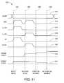
- FIG. 11provides a timing diagram for the operation of the circuit of FIG. 9 .
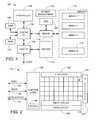
- FIG. 1provides a functional block representation of a data storage device 100 constructed and operated in accordance with various embodiments of the present invention.
- the data storage deviceis contemplated as comprising a portable non-volatile memory storage device such as a PCMCIA card or USB-style external memory device. It will be appreciated, however, that such characterization of the device 100 is merely for purposes of illustration and is not limiting to the claimed subject matter.
- Top level control of the device 100is carried out by a suitable controller 102 , which may be a programmable or hardware based microcontroller.
- the controller 102communicates with a host device via a controller interface (I/F) circuit 104 and a host I/F circuit 106 .
- I/Fcontroller interface
- Local storage of requisite commands, programming, operational data, etc.is provided via random access memory (RAM) 108 and read-only memory (ROM) 110 .
- RAMrandom access memory
- ROMread-only memory
- a buffer 112serves to temporarily store input write data from the host device and readback data pending transfer to the host device, as well as to facilitate serialization/deserialization of the data during a transfer operation.
- the buffercan be located in any suitable location, including in a portion of the array.
- a memory spaceis shown at 114 to comprise a number of memory arrays 116 (denoted Array 0-N), although it will be appreciated that a single array can be utilized as desired.
- Each array 116preferably comprises a block of semiconductor memory of selected storage capacity.
- Communications between the controller 102 and the memory space 114are coordinated via a memory (MEM) I/F 118 .
- EDCerror detection and correction
- encoding and decoding operationsare carried out during data transfers by way of an EDC block 120 .
- the various circuits depicted in FIG. 1are arranged as a single chip set formed on one or more semiconductor dies with suitable encapsulation, housing and interconnection features (not separately shown for purposes of clarity).
- Input power to operate the deviceis handled by a suitable power management circuit 122 and is supplied from a suitable source such as from a battery, AC power input, etc. Power can also be supplied to the device 100 directly from the host such as through the use of a USB-style interface, etc.
- LBAslogical block addressing
- Host commandscan be issued in terms of LBAs, and the device 100 can carry out a corresponding LBA-to-PBA (physical block address) conversion to identify and service the associated locations at which the data are to be stored or retrieved.
- LBA-to-PBAphysical block address
- FIG. 2provides a generalized representation of selected aspects of the memory space 114 of FIG. 1 .
- Dataare stored as an arrangement of rows and columns of memory cells 124 , accessible by various row (word) and column (bit) lines, etc.
- each of the array memory cells 124has a spin-torque transfer random access memory (STTRAM or STRAM) configuration.
- STTRAMspin-torque transfer random access memory
- non-volatile or volatile memory cell constructionsincluding but not limited to resistive RAM (RRAM), magnetoresistive RAM (MRAM), zero-capacitor RAM (ZRAM), static RAM (SRAM), non-volatile static RAM (nvSRAM), ferroelectric RAM (FeRAM), nano RAM (NRAM), phase-change RAM (PRAM), EEPROM, flash, dynamic RAM (DRAM), etc.
- RRAMresistive RAM
- MRAMmagnetoresistive RAM
- ZRAMzero-capacitor RAM
- SRAMstatic RAM
- nvSRAMnon-volatile static RAM
- FeRAMferroelectric RAM
- NRAMnano RAM
- PRAMphase-change RAM
- EEPROMelectrically erasable programmable read-only memory
- flashdynamic RAM
- DRAMdynamic RAM
- control lineswill generally include enable lines that selectively enable and disable the respective writing and reading of the value(s) of the individual cells.
- Control logic 126receives and transfers data, addressing information and control/status values along multi-line bus paths 128 , 130 and 132 , respectively.
- X and Y decoding circuitry 134 , 136provide appropriate switching and other functions to access the appropriate cells 124 .
- a write circuit 138represents circuitry elements that operate to carry out write operations to write data to the cells 124 , and a read circuit 140 correspondingly operates to obtain readback data from the cells 124 .
- Local buffering of transferred data and other valuescan be provided via one or more local registers 144 .
- the circuitry of FIG. 2is merely exemplary in nature, as any number of alternative configurations can readily be employed as desired depending on the requirements of a given application.
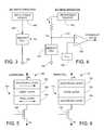
- a write power source 146applies the necessary input (such as in the form of current, voltage, magnetization, etc.) to configure the memory cell 124 to a desired state.
- the configuration of the write power source 146 , memory cell 124 , and reference node 148can be suitably manipulated to allow conventional writing of a bit with a variety of memory devices (such as SRAM, STRAM, RRAM, flash, etc).
- the memory cell 124takes an STRAM configuration, in which case the write power source 146 is preferably characterized as a bi-directional current driver connected through a memory cell 124 to a suitable reference node 148 , such as ground.
- the write power source 146preferably provides a stream of power that is spin polarized by moving through a magnetic material in the memory cell 124 . The resulting rotation of the polarized spins creates a torque that changes the magnetic moment of the memory cell 124 .
- the cell 124may take either a relatively low resistance (R L ) or a relatively high resistance (R H ). While not limiting, exemplary R L values may be in the range of about 2000 ohms ( ⁇ ) or so, whereas exemplary R H values may be in the range of about 100K ⁇ or so. Other resistive memory type configurations (e.g., RRAMs) are supplied with a suitable voltage or other input to similarly provide respective R L and R H values. These values are retained by the respective cells until such time that the state is changed by a subsequent write operation. While not limiting, in the present example it is contemplated that a high resistance value (R H ) denotes storage of a logical 1 by the cell 124 , and a low resistance value (R L ) denotes storage of a logical 0.
- R Hhigh resistance value
- R Llow resistance value
- the logical bit value(s) stored by each cell 124can be determined in a manner such as illustrated by FIG. 4 .
- a read power source 150applies an appropriate input (e.g., a selected read voltage) to the memory cell 124 .
- the amount of read current I R that flows through the cell 124will be a function of the resistance of the cell (R L or R H , respectively). In the case of STRAM, as well as other types of memory configurations such as RRAM, the read current magnitude will generally be significantly lower than the write current magnitude utilized to set the storage state of the bit.
- the voltage drop across the memory cell(voltage V MC ) is sensed via path 152 by the positive (+) input of a comparator 154 .
- a suitable reference(such as voltage reference V REF ) is supplied to the negative ( ⁇ ) input of the comparator 154 from a reference source 156 .
- the reference voltage V REFis preferably selected such that the voltage drop V MC across the memory cell 124 will be lower than the V REF value when the resistance of the cell is set to R L , and will be higher than the V REF value when the resistance of the cell is set to R H . In this way, the output voltage level of the comparator 154 will indicate the logical bit value (0 or 1) stored by the memory cell 124 .
- the memory cells 124are characterized as so-called resistive sense memory (RSM) cells.
- RSM cellsare generally described as cells configured to have different electrical resistances which are used to store different logical states. The resistance of the cells can be subsequently detected during a read operation by applying a read current and sensing a signal in relation to a voltage drop across the cell.
- Exemplary types of RSM cellsinclude STRAM, RRAM, magnetic random access memory (MRAM), etc.
- RSM cellsover other types of non-volatile memory cells such as EEPROM and flash include the fact that no floating gate is provided in the cell construction. No erase operation is necessary prior to the writing of new data to an existing set of cells. Rather, RSM cells can be individually accessed and written to any desired logical state (e.g., a “0” or “1”) irrespective of the existing state of the RSM cell. Also, write and read power consumption requirements are substantially reduced, significantly faster write and read times can be achieved, and substantially no wear degradation is observed as compared to erasable cells, which have a limited write/erase cycle life.
- FIG. 5shows an exemplary STRAM cell 160 .
- the STRAM cell 160includes a magnetic tunneling junction (MTJ) 161 formed from two ferromagnetic layers 162 , 164 separated by an oxide barrier layer 166 (such as magnesium oxide, MgO).
- the resistance of the MTJ 161is determined in relation to the relative magnetization directions of the ferromagnetic layers 162 , 164 : when the magnetization is in the same direction, the MTJ is in the low resistance state (R L ); when the magnetization is in opposite directions, the MTJ is in the high resistance state (R H ).
- the magnetization direction of the reference layer 162is fixed by coupling to a pinned magnetization layer (e.g., a permanent magnet, etc.), and the magnetization direction of the free layer 164 can be changed by passing a driving current polarized by magnetization in the reference layer 162 .
- a pinned magnetization layere.g., a permanent magnet, etc.
- a switching device 168allows selective access to the MTJ 161 during read and write operations.
- FIG. 6illustrates an RRAM cell 170 as an alternative RSM cell construction.
- the RRAM cell 170provides a resistive sense element 171 with opposing electrode layers 172 , 174 and an oxide layer 176 .
- the oxide layer 176may be configured to have a nominally high resistance (e.g., R H ).
- the resistance of the oxide layercan be lowered (e.g., R L ) through application of a relatively high write voltage across the RRAM cell 170 .
- Such voltagegenerates lower resistance paths (filaments) as components of a selected electrode layer 172 , 174 migrate into the oxide layer 176 .
- the oxide layer 176can be restored to its original, higher resistance through application of a corresponding voltage of opposite polarity.
- the storage state of the RRAM cell 170 of FIG. 6can be read by passing a read current from a source line (SL) to a bit line (BL), and sensing the resistance of the cell in a manner such as shown in FIG. 4 .
- a switching device 178facilitates access to the RRAM cell.
- the sensing of the programmed resistive state of an RSM cellshould be carried out in such a way as to accurately and reliably distinguish between the high and low resistive states.
- V MINI R ( R MIN +R TR ) (2) where V MIN is the sensed voltage, I R is the read current, R MIN is the programmed low resistance of the resistive sense element (such as MTJ 161 in FIG. 5 ), and R TR is the drain-to-source resistance of the transistor (such as the device 168 in FIG. 5 ).
- V REFreference voltage
- V MAX >V REF >V MINa reference voltage V REF that is suitable for resistive state detection of some cells within the array may not be suitable for resistive state detection in other cells. This may lead to incorrect detection of the resistive state of the cells, and erroneous data being read back from the array.
- various embodiments of the present inventionare generally directed to providing a dual stage self-reference sensing scheme for the memory cells in a resistive sense memory array.
- the schemegenerally applies different magnitudes of read currents to a memory cell. This provides different readback voltages that are compared to discern the resistive state of the cell.
- a dual-stage sense amplifier structureis further used to improve the efficiency of the voltage sense operation.
- FIG. 7provides a voltage-current (V-I) curve 180 for a selected RSM cell 124 , in this case the STRAM cell 160 of FIG. 5 .
- the curve 180is plotted against a current magnitude x-axis 182 and a resistance magnitude y-axis 184 .
- a first portion 186 of the curve 180represents the resistance of the STRAM cell 160 when the MTJ 161 is programmed to the high resistance R MAX . That is, for various applied read currents, the portion 182 shows the corresponding resistance of the STRAM cell 160 when the MTJ 161 is programmed to the high resistance.
- a second portion 188 of the curve 180represents the resistance of the STRAM cell 160 when the MTJ 161 is programmed to the low resistance R MIN .
- the R MIN portion 188is relatively flat (i.e., has a substantially smaller slope) as compared to the R MAX portion 186 . Applying a selected magnitude of read current I R to the cell 160 will provide different voltages corresponding to the different possible programmed resistances (R MIN or R MAX ) of the MTJ 161 .
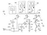
- FIG. 8shows a read circuit 200 configured in accordance with various embodiments to read the programmed resistive state of the STRAM cell 160 of FIG. 7 .
- the circuitincludes a number of components which will be initially identified prior to an explanation of the operation of the circuit. These components include first and second capacitors 202 , 204 (C 1 and C 2 ); a number of switching devices 206 , 208 , 210 and 212 (S 1 -S 4 ); first and second resistors 214 , 216 (R 1 and R 2 ); a sense amplifier 218 ; first and second current sources 220 , 222 ; and a pre-charge source 224 .
- the S 1 -S 4 switching devicesare characterized as NMOS transistors, although other configurations can be used.
- the S 1 device 206allows individual selection of the cell 160 , and is asserted via a decoder line 226 . Only a single stage sense amplifier 218 is shown in FIG. 8 to facilitate the present discussion; a more complex, and faster response dual stage sense amplifier arrangement will be discussed below.
- a bit line (BL) 228 coupled to the cell 160is pre-charged with a voltage V PRE from the pre-charge source 224 . While optional, such pre-charging can improve the speed at which the cell 160 is read.
- a word line 230 (WL)is asserted to place the cell transistor 168 in a drain-to-source conductive state
- the decoder line 226is asserted to place the S 1 device 206 in a conductive state
- a first read current I Ris applied to the cell 160 from the first read current source 220 .
- the first read current source 220includes a current driver 232 and a switching device 234 . Assertion of the switching device 234 allows the first read current I R to pass from the driver 232 to the BL 228 and through the MTJ 161 to ground.
- the voltage at the BL 228will be proportional to the voltage drop across the MTJ 161 .
- this voltagewill also include the small forward conduction drops across the S 1 device 206 and the cell transistor 168 , but these will be relatively small compared to the voltage drop across the MTJ 161 , and will be substantially the same each time current is applied to the cell.
- the voltage on the BL 228 resulting from the first read current I Rcan be used as an indication of the voltage drop across the MTJ 161 , and hence, the programmed state thereof.
- the S 2 switching device 208is asserted so that the voltage on the BL 228 is stored on the C 1 capacitor 202 .
- the S 2 switching deviceis deasserted to retain this voltage on the C 1 capacitor.
- a second read current I R ′is applied to the BL 228 from the second current source 222 via current driver 236 and switching device 238 .
- the second read current I R ′also results in a voltage being presented on the BL 228 .
- the S 3 and S 4 switching devices 210 , 212are asserted, so that a second voltage is stored on the C 2 capacitor 204 that is proportional to both the voltage drop across the MTJ 161 , as well as the voltage divider formed by the R 1 and R 2 resistors 214 , 216 . That is the voltage across the MTJ 161 is divided by the ratio of the R 1 and R 2 resistors 214 , 216 so that the second voltage substantially corresponds to the voltage at a node 240 between the R 1 and R 2 resistors.
- This second voltage V 2generally constitutes a reference voltage V REF for the first voltage V 1 stored on the C 1 capacitor 202 .
- the first and second voltages V 1 and V 2 on the respective C 1 and C 2 capacitors 202 , 204are compared through provision of the voltages to respective input terminals of the sense amplifier 218 . This comparison results in the generation of a sense amplifier output (SA OUT ) indicative of the storage state of the MTJ 161 .
- SA OUTsense amplifier output
- the ability of the sense amplifier 218 to correctly discern the storage state of the MTJ 161will depend on a number of factors, including the respective values for the first and second read currents I R and I R ′ and the respective resistance values of the R 1 and R 2 resistors 214 , 216 . Referring again to FIG. 7 , it will be recalled that the voltage portion 188 for R MIN is substantially flat.
- R MIN value for the first read current I Rwill be substantially equal to the R MIN ′ value for the second read current I R ′, that is, R MIN ⁇ R MIN ′ (4)
- the forward resistance of the cell transistor 168 R TRwill be substantially the same for both read currents since the transistor will be operating in the linear region in both cases, so R TR ⁇ R TR ′ (5)
- the second voltage V 2 stored on the C 2 capacitor 204can be generally expressed as:
- V 2I R ′ ⁇ ( R MIN ′ + R TR ′ ) ⁇ R ⁇ ⁇ 2 ( R ⁇ ⁇ 1 + R ⁇ ⁇ 2 ) ( 7 ) If the respective magnitudes of R 1 and R 2 are selected to provide
- V 1I R ( R MAX +R TR ) (10)
- V 2I R ( R MAX +R TR ) (10)
- V 2I R ′ ⁇ ( R MAX ′ + R TR ′ ) ⁇ R ⁇ ⁇ 2 ( R ⁇ ⁇ 1 + R ⁇ ⁇ 2 ) ( 11 )
- the voltage differential between the voltages V1 and V2 on the respective C 1 and C 2 capacitors 202 , 204will be substantially greater than zero when the MTJ 161 in FIG. 8 is programmed to the high resistance R MAX .
- a small threshold valuee.g., ⁇ >0
- ⁇ >0can be used to discern whether the difference between the respective voltages V 1 and V 2 is large enough to indicate that the programmed state of the MTJ is high.
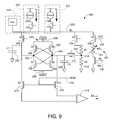
- FIG. 9provides an alternative read circuit 250 configured in accordance with various embodiments to read the programmed resistive state of the STRAM cell 160 .
- the read circuit 250is generally similar to the circuit 200 of FIG. 8 , and like reference numerals are used for similar components in each of the figures.
- FIG. 9includes a cross-coupled differential sense amplifier circuit 252 .
- the circuit 252operates as an upstream, first stage amplifier circuit to initially sense the voltage differential between the V 1 and V 2 voltages to a certain differential range (opening), after which the downstream second stage amplifier 218 is activated to pull the differential to full swing.
- the first stage amplifier circuit 252comprises four cross-connected switching devices 254 , 256 , 258 and 260 denoted as S 5 through S 8 .
- the S 5 and S 6 devices 254 , 256are characterized as PMOS transistors, and the S 7 and S 8 devices 258 , 260 are characterized as NMOS transistors, although other configurations can be used.
- a first terminal, or sense node 262is coupled to the C 1 capacitor 202
- a second terminal, or sense node 264is coupled to the C 2 capacitor 204 .
- Suitable rail voltagesare supplied to the circuit 252 via a positive voltage range (PRVG) source 266 and a negative voltage range (NVRG) source 268 .
- a pair of switching devices (NMOS transistors) 270 , 272are denoted as S 9 and S 10 and are respectively coupled to the sense nodes 262 and 264 .
- the devices 270 , 272are asserted via a MUX line 274 to connect the first stage sense circuit 252 to the second stage sense amplifier 218 .
- additional switching circuitrycan be used to share the second stage sense amplifier 218 among multiple first stage sense amplifiers 252 .
- the circuit 250 of FIG. 9operates substantially as described above to provide V1 and V2 voltages on the C 1 and C 2 capacitors 202 , 204 responsive to successively applied, first and second read currents I R and I R ′.
- the voltage differential between sense nodes 262 and 264will be enhanced in relation to differences between the V1 and V2 voltages, so that when the second stage amplifier 218 is switched in via MUX line 274 , the final SA OUT value can be quickly obtained.
- FIG. 10shows an exemplary programmable current driver circuit 280 that can be advantageously used to generate the first and second I R and I R ′ read currents.
- the circuit 280 in FIG. 10thus constitutes one possible implementation of both current drivers 232 and 236 in FIGS. 8-9 . Other configurations can readily be used, however.
- the driver circuit 280is connected across a voltage V DD from a source 282 and a reference level 284 , such as ground.
- Switching devices 286 , 288configured as PMOS transistors and denoted as S 11 and S 12 , are coupled to the source 282 as shown.
- An output line 290provides the commanded current.
- Two parallel sets of switching devices S 13 -S 18are coupled between the S 11 -S 12 devices and ground 284 . These S 13 -S 18 devices are individually denoted at 292 , 293 , 294 , 295 , 296 and 297 , respectively.
- the S 13 -S 15 deviceshave gates concurrently asserted by a first current enable signal (I R — EN) on path 298 , and the S 16 -S 18 devices are similarly asserted by a second current enable signal (I R ′ — EN) on path 299 .
- the driver circuit 280outputs the first read current I R responsive to magnitude of the I R — EN signal (first gate voltage), and the driver circuit 280 outputs the second read current I R responsive to the magnitude of the I R ′ — EN signal (second gate voltage).
- a common driver circuit 280can be configured to separately provide different respective first and second read currents for different cells.
- multi-bit digital values representative of the desired read current magnitudescan be stored in a suitable location in memory, and supplied to a digital-to-analog converter (DAC, not shown) to generate the respective currents.
- DACdigital-to-analog converter
- FIG. 11sets forth an exemplary timing diagram 300 for various signals utilized in the operation of the circuit 250 of FIG. 9 . It will be appreciated that aspects of the timing diagram of FIG. 11 are also applicable to the operation of the circuit 200 of FIG. 8 .
- the diagram 300is generally divided into four time intervals which are bounded by vertically extending dashed lines 302 , 304 , 306 and 308 . These time intervals will generally occur at appropriate times during the read operation, and may not necessarily be equally spaced in the manner shown in FIG. 11 .
- the first time interval between lines 302 and 304constitutes the first read operation on the MTJ 161 using the first read current I R .
- the second time interval ( 304 - 306 )constitutes the second read operation on the MTJ 161 using the second read current I R ′.
- the third time interval ( 306 - 308 )is a first stage sensing operation using the first stage sense amplifier circuit 252
- the fourth time interval ( 308 and beyond)represents the second stage operation using the output sense amplifier 218 .
- a complementary address (ADDR) signal 310generally serves as a read gate to initialize the read operation upon the selected cell 160 .
- the ADDR signal 310is asserted during the entirety of the read operation.
- a decoder (DEC) signal 312asserts the S 1 device 206 in FIG. 9 at the appropriate times to allow passage of the respective first and second read currents, as indicated by I R — EN and I R ′ — EN signals 314 and 316 (see FIG. 10 ).
- the S 2 device 208( FIG. 9 ) is asserted during the first time interval as shown by signal 318 , thereby allowing the V1 voltage to be stored on the C 1 capacitor 202 .
- the S 3 and S 4 devices 210 , 212( FIG. 9 ) are asserted during the second time interval as shown by signal 320 , allowing the V2 voltage to be stored on the C 2 capacitor 204 .
- FIG. 11further shows respective sense response signals SENSE (HIGH) 322 and SENSE (LOW) 324 .
- SENSEHIGH
- SENSELOW
- These signals 322 , 324indicate the sensing levels by the dual stage sense circuits 252 and 218 ( FIG. 9 ) during the read operation.
Landscapes
- Engineering & Computer Science (AREA)
- Computer Hardware Design (AREA)
- Mram Or Spin Memory Techniques (AREA)
- Semiconductor Memories (AREA)
- Hall/Mr Elements (AREA)
Abstract
Description
VMAX=IR(RMAX+RTR) (1)
where VMAXis the sensed voltage, IRis the read current, RMAXis the programmed high resistance of the resistive sense element (such as
VMIN=IR(RMIN+RTR) (2)
where VMINis the sensed voltage, IRis the read current, RMINis the programmed low resistance of the resistive sense element (such as
ΔV=VMAX−VMIN=IR(RMAX−RMIN) (3)
The voltage differential ΔV constitutes the available margin for resistive state detection.
RMIN≈RMIN′ (4)
The forward resistance of the cell transistor168 RTRwill be substantially the same for both read currents since the transistor will be operating in the linear region in both cases, so
RTR≈RTR′ (5)
V1=IR(RMIN+RTR) (6)
The second voltage V2stored on the
If the respective magnitudes of R1 and R2 are selected to provide
then combining equations (6) and (7) provides
V1−V2=IR(RMIN−RMIN′)≈0 (9)
V1=IR(RMAX+RTR) (10)
The second voltage V2stored on the
V1−V2=IR(RMAX−RMAX′)>>0 (12)
Claims (20)
Priority Applications (1)
| Application Number | Priority Date | Filing Date | Title |
|---|---|---|---|
| US12/946,582US8203899B2 (en) | 2008-10-31 | 2010-11-15 | Memory cell with proportional current self-reference sensing |
Applications Claiming Priority (3)
| Application Number | Priority Date | Filing Date | Title |
|---|---|---|---|
| US10996708P | 2008-10-31 | 2008-10-31 | |
| US12/406,356US7852665B2 (en) | 2008-10-31 | 2009-03-18 | Memory cell with proportional current self-reference sensing |
| US12/946,582US8203899B2 (en) | 2008-10-31 | 2010-11-15 | Memory cell with proportional current self-reference sensing |
Related Parent Applications (1)
| Application Number | Title | Priority Date | Filing Date |
|---|---|---|---|
| US12/406,356ContinuationUS7852665B2 (en) | 2008-10-31 | 2009-03-18 | Memory cell with proportional current self-reference sensing |
Publications (2)
| Publication Number | Publication Date |
|---|---|
| US20110058405A1 US20110058405A1 (en) | 2011-03-10 |
| US8203899B2true US8203899B2 (en) | 2012-06-19 |
Family
ID=42131201
Family Applications (2)
| Application Number | Title | Priority Date | Filing Date |
|---|---|---|---|
| US12/406,356Expired - Fee RelatedUS7852665B2 (en) | 2008-10-31 | 2009-03-18 | Memory cell with proportional current self-reference sensing |
| US12/946,582Expired - Fee RelatedUS8203899B2 (en) | 2008-10-31 | 2010-11-15 | Memory cell with proportional current self-reference sensing |
Family Applications Before (1)
| Application Number | Title | Priority Date | Filing Date |
|---|---|---|---|
| US12/406,356Expired - Fee RelatedUS7852665B2 (en) | 2008-10-31 | 2009-03-18 | Memory cell with proportional current self-reference sensing |
Country Status (1)
| Country | Link |
|---|---|
| US (2) | US7852665B2 (en) |
Cited By (15)
| Publication number | Priority date | Publication date | Assignee | Title |
|---|---|---|---|---|
| US8654561B1 (en)* | 2010-10-29 | 2014-02-18 | Adesto Technologies Corporation | Read methods, circuits and systems for memory devices |
| US8742830B2 (en)* | 2012-07-19 | 2014-06-03 | Globalfoundries Singapore Pte. Ltd. | Fuse sensing circuits |
| US20150228322A1 (en)* | 2014-02-12 | 2015-08-13 | Industry-Academic Cooperation Foundation, Yonsei University | Nmos-offset canceling current-latched sense amplifier |
| US9165630B2 (en) | 2013-08-30 | 2015-10-20 | Qualcomm Incorporated | Offset canceling dual stage sensing circuit |
| US9281043B1 (en)* | 2014-12-24 | 2016-03-08 | Intel Corporation | Resistive memory write circuitry with bit line drive strength based on storage cell line resistance |
| CN107342104A (en)* | 2016-04-29 | 2017-11-10 | 上海磁宇信息科技有限公司 | A kind of asymmetric magnetic RAM and its Magnetic memory cell reading method |
| US20180301198A1 (en)* | 2017-04-14 | 2018-10-18 | Shine C. Chung | Low power read operation for programmable resistive memories |
| US10586593B2 (en) | 2012-12-07 | 2020-03-10 | Attopsemi Technology Co., Ltd | Programmable resistive device and memory using diode as selector |
| US10726914B2 (en) | 2017-04-14 | 2020-07-28 | Attopsemi Technology Co. Ltd | Programmable resistive memories with low power read operation and novel sensing scheme |
| US10770160B2 (en) | 2017-11-30 | 2020-09-08 | Attopsemi Technology Co., Ltd | Programmable resistive memory formed by bit slices from a standard cell library |
| US10916317B2 (en) | 2010-08-20 | 2021-02-09 | Attopsemi Technology Co., Ltd | Programmable resistance memory on thin film transistor technology |
| US10923204B2 (en) | 2010-08-20 | 2021-02-16 | Attopsemi Technology Co., Ltd | Fully testible OTP memory |
| US11011577B2 (en) | 2011-02-14 | 2021-05-18 | Attopsemi Technology Co., Ltd | One-time programmable memory using gate-all-around structures |
| US11062786B2 (en) | 2017-04-14 | 2021-07-13 | Attopsemi Technology Co., Ltd | One-time programmable memories with low power read operation and novel sensing scheme |
| US11615859B2 (en) | 2017-04-14 | 2023-03-28 | Attopsemi Technology Co., Ltd | One-time programmable memories with ultra-low power read operation and novel sensing scheme |
Families Citing this family (37)
| Publication number | Priority date | Publication date | Assignee | Title |
|---|---|---|---|---|
| JP2010079974A (en)* | 2008-09-25 | 2010-04-08 | Toshiba Corp | Semiconductor memory device |
| US7852665B2 (en)* | 2008-10-31 | 2010-12-14 | Seagate Technology Llc | Memory cell with proportional current self-reference sensing |
| US8370714B2 (en)* | 2010-01-08 | 2013-02-05 | International Business Machines Corporation | Reference cells for spin torque based memory device |
| US8374020B2 (en) | 2010-10-29 | 2013-02-12 | Honeywell International Inc. | Reduced switching-energy magnetic elements |
| US8427199B2 (en) | 2010-10-29 | 2013-04-23 | Honeywell International Inc. | Magnetic logic gate |
| US8358149B2 (en) | 2010-10-29 | 2013-01-22 | Honeywell International Inc. | Magnetic logic gate |
| US8358154B2 (en)* | 2010-10-29 | 2013-01-22 | Honeywell International Inc. | Magnetic logic gate |
| US8605521B2 (en) | 2011-05-12 | 2013-12-10 | Micron Technology, Inc. | Sense amplifiers, memories, and apparatuses and methods for sensing a data state of a memory cell |
| US8427197B2 (en) | 2011-06-15 | 2013-04-23 | Honeywell International Inc. | Configurable reference circuit for logic gates |
| EP2740123A4 (en)* | 2011-08-02 | 2015-07-22 | Univ Ramot | Multi-bit magnetic memory cell |
| CN103858168B (en)* | 2011-09-02 | 2016-09-28 | 慧与发展有限责任合伙企业 | For storing the equipment of data and for the method reading memory element |
| US8923041B2 (en) | 2012-04-11 | 2014-12-30 | Everspin Technologies, Inc. | Self-referenced sense amplifier for spin torque MRAM |
| US9111622B2 (en) | 2012-05-09 | 2015-08-18 | Everspin Technologies, Inc. | Self referencing sense amplifier for spin torque MRAM |
| GB2502553A (en)* | 2012-05-30 | 2013-12-04 | Ibm | Read measurements of resistive memory cells |
| US20150187414A1 (en)* | 2012-07-27 | 2015-07-02 | Hewlett-Packard Development Company, L.P. | Dynamic sense circuitry |
| US8693240B1 (en)* | 2012-11-28 | 2014-04-08 | Avalanche Technology, Inc. | Method and apparatus for reading a magnetic tunnel junction using a sequence of short pulses |
| TWI524718B (en) | 2012-12-06 | 2016-03-01 | 財團法人資訊工業策進會 | Major management apparatus, authorized management apparatus, electronic apparatus for delegated key management, and key management methods thereof |
| TWI456427B (en) | 2012-12-12 | 2014-10-11 | Inst Information Industry | Major management apparatus, authorized management apparatus, electronic apparatus for delegation management, and delegation management methods thereof |
| US9378821B1 (en)* | 2013-01-18 | 2016-06-28 | Cypress Semiconductor Corporation | Endurance of silicon-oxide-nitride-oxide-silicon (SONOS) memory cells |
| US9627024B2 (en) | 2013-09-19 | 2017-04-18 | University of Pittsburgh—of the Commonwealth System of Higher Education | Magnetic-assisted nondestructive self-reference sensing method for spin-transfer torque random access memory |
| EP3114690B1 (en)* | 2014-03-07 | 2020-02-12 | Intel Corporation | Physically unclonable function circuit using resistive memory device |
| WO2016018281A1 (en)* | 2014-07-30 | 2016-02-04 | Hewlett-Packard Development Company, L.P. | Current behavior of elements |
| US9281041B1 (en)* | 2014-12-16 | 2016-03-08 | Honeywell International Inc. | Delay-based read system for a magnetoresistive random access memory (MRAM) bit |
| JP6824504B2 (en) | 2015-03-06 | 2021-02-03 | 株式会社BlueSpin | Magnetic memory, data writing method to magnetic memory and semiconductor device |
| JP2016194964A (en) | 2015-04-01 | 2016-11-17 | 株式会社BlueSpin | Magnetic memory and operation method thereof |
| US9748943B2 (en)* | 2015-08-13 | 2017-08-29 | Arm Ltd. | Programmable current for correlated electron switch |
| US10573363B2 (en)* | 2015-12-02 | 2020-02-25 | Samsung Electronics Co., Ltd. | Method and apparatus for performing self-referenced read in a magnetoresistive random access memory |
| US9721636B1 (en)* | 2016-01-28 | 2017-08-01 | Western Digital Technologies, Inc. | Method for controlled switching of a MRAM device |
| US9679643B1 (en) | 2016-03-09 | 2017-06-13 | Taiwan Semiconductor Manufacturing Co., Ltd. | Resistive memory device having a trimmable resistance of at least on of a driver and a sinker is trimmed based on a row location |
| DE102016110049A1 (en)* | 2016-05-31 | 2017-11-30 | Infineon Technologies Ag | Determining a state of a memory cell |
| JP2019057348A (en) | 2017-09-21 | 2019-04-11 | 東芝メモリ株式会社 | Memory device |
| US10290327B2 (en)* | 2017-10-13 | 2019-05-14 | Nantero, Inc. | Devices and methods for accessing resistive change elements in resistive change element arrays |
| US10515679B2 (en)* | 2018-02-06 | 2019-12-24 | Globalfoundries Inc. | Magneto-resistive memory structures with improved sensing, and associated sensing methods |
| US11031400B2 (en)* | 2018-08-10 | 2021-06-08 | Micron Technology, Inc. | Integrated memory comprising secondary access devices between digit lines and primary access devices |
| US10818349B2 (en)* | 2018-09-27 | 2020-10-27 | Taiwan Semiconductor Manufacturing Co., Ltd. | Programming method and reading method for memory device |
| US11374057B2 (en)* | 2020-06-23 | 2022-06-28 | Taiwan Semiconductor Manufacturing Company Limited | Vertical metal oxide semiconductor channel selector transistor and methods of forming the same |
| US12243614B2 (en) | 2022-10-17 | 2025-03-04 | Globalfoundries U.S. Inc. | Single ended sense amplifier with current pulse circuit |
Citations (20)
| Publication number | Priority date | Publication date | Assignee | Title |
|---|---|---|---|---|
| US5875134A (en) | 1995-08-30 | 1999-02-23 | Micron Technology, Inc. | Data communication for memory |
| US6005816A (en) | 1997-07-24 | 1999-12-21 | Micron Technology, Inc. | Sense amplifier for complementary or non-complementary data signals |
| US6118326A (en) | 1997-11-06 | 2000-09-12 | Analog Devices, Inc. | Two-phase bootstrapped CMOS switch drive technique and circuit |
| US6243291B1 (en) | 2000-02-15 | 2001-06-05 | Advanced Micro Devices, Inc. | Two-stage pipeline sensing for page mode flash memory |
| US6584003B1 (en) | 2001-12-28 | 2003-06-24 | Mosaid Technologies Incorporated | Low power content addressable memory architecture |
| US6728128B2 (en) | 2002-03-19 | 2004-04-27 | Texas Instrument Incorporated | Dummy cell structure for 1T1C FeRAM cell array |
| US6765820B2 (en)* | 2000-07-18 | 2004-07-20 | Micron Technology, Inc. | Magneto-resistive memory array |
| US7099180B1 (en)* | 2005-02-15 | 2006-08-29 | Intel Corporation | Phase change memory bits reset through a series of pulses of increasing amplitude |
| US7116576B2 (en) | 2003-07-07 | 2006-10-03 | Hewlett-Packard Development Company, L.P. | Sensing the state of a storage cell including a magnetic element |
| US7154774B2 (en) | 2005-03-30 | 2006-12-26 | Ovonyx, Inc. | Detecting switching of access elements of phase change memory cells |
| US7161861B2 (en) | 2004-11-15 | 2007-01-09 | Infineon Technologies Ag | Sense amplifier bitline boost circuit |
| US7266029B2 (en) | 2004-09-30 | 2007-09-04 | Samsung Electronics Co Ltd | Nonvolatile memory devices including overlapped data sensing and verification and methods of verifying data in nonvolatile memory devices |
| US7286394B2 (en) | 2004-07-14 | 2007-10-23 | Renesas Technology Corp. | Non-volatile semiconductor memory device allowing concurrent data writing and data reading |
| US20080056023A1 (en) | 2006-09-04 | 2008-03-06 | Samsung Electronics Co., Ltd. | Nonvolatile memory device and related methods of operation |
| US7345912B2 (en) | 2006-06-01 | 2008-03-18 | Grandis, Inc. | Method and system for providing a magnetic memory structure utilizing spin transfer |
| US7561461B2 (en) | 2007-02-28 | 2009-07-14 | Panasonic Corporation | Non-volatile semiconductor memory device |
| US20090323402A1 (en) | 2008-06-27 | 2009-12-31 | Seagate Technology Llc | Spin-transfer torque memory self-reference read method |
| US20090323403A1 (en) | 2008-06-27 | 2009-12-31 | Seagate Technology Llc | Spin-transfer torque memory non-destructive self-reference read method |
| US20100110760A1 (en) | 2008-10-31 | 2010-05-06 | Seagate Technology Llc | Resistive Sense Memory Calibration for Self-Reference Read Method |
| US7852665B2 (en)* | 2008-10-31 | 2010-12-14 | Seagate Technology Llc | Memory cell with proportional current self-reference sensing |
- 2009
- 2009-03-18USUS12/406,356patent/US7852665B2/ennot_activeExpired - Fee Related
- 2010
- 2010-11-15USUS12/946,582patent/US8203899B2/ennot_activeExpired - Fee Related
Patent Citations (20)
| Publication number | Priority date | Publication date | Assignee | Title |
|---|---|---|---|---|
| US5875134A (en) | 1995-08-30 | 1999-02-23 | Micron Technology, Inc. | Data communication for memory |
| US6005816A (en) | 1997-07-24 | 1999-12-21 | Micron Technology, Inc. | Sense amplifier for complementary or non-complementary data signals |
| US6118326A (en) | 1997-11-06 | 2000-09-12 | Analog Devices, Inc. | Two-phase bootstrapped CMOS switch drive technique and circuit |
| US6243291B1 (en) | 2000-02-15 | 2001-06-05 | Advanced Micro Devices, Inc. | Two-stage pipeline sensing for page mode flash memory |
| US6765820B2 (en)* | 2000-07-18 | 2004-07-20 | Micron Technology, Inc. | Magneto-resistive memory array |
| US6584003B1 (en) | 2001-12-28 | 2003-06-24 | Mosaid Technologies Incorporated | Low power content addressable memory architecture |
| US6728128B2 (en) | 2002-03-19 | 2004-04-27 | Texas Instrument Incorporated | Dummy cell structure for 1T1C FeRAM cell array |
| US7116576B2 (en) | 2003-07-07 | 2006-10-03 | Hewlett-Packard Development Company, L.P. | Sensing the state of a storage cell including a magnetic element |
| US7286394B2 (en) | 2004-07-14 | 2007-10-23 | Renesas Technology Corp. | Non-volatile semiconductor memory device allowing concurrent data writing and data reading |
| US7266029B2 (en) | 2004-09-30 | 2007-09-04 | Samsung Electronics Co Ltd | Nonvolatile memory devices including overlapped data sensing and verification and methods of verifying data in nonvolatile memory devices |
| US7161861B2 (en) | 2004-11-15 | 2007-01-09 | Infineon Technologies Ag | Sense amplifier bitline boost circuit |
| US7099180B1 (en)* | 2005-02-15 | 2006-08-29 | Intel Corporation | Phase change memory bits reset through a series of pulses of increasing amplitude |
| US7154774B2 (en) | 2005-03-30 | 2006-12-26 | Ovonyx, Inc. | Detecting switching of access elements of phase change memory cells |
| US7345912B2 (en) | 2006-06-01 | 2008-03-18 | Grandis, Inc. | Method and system for providing a magnetic memory structure utilizing spin transfer |
| US20080056023A1 (en) | 2006-09-04 | 2008-03-06 | Samsung Electronics Co., Ltd. | Nonvolatile memory device and related methods of operation |
| US7561461B2 (en) | 2007-02-28 | 2009-07-14 | Panasonic Corporation | Non-volatile semiconductor memory device |
| US20090323402A1 (en) | 2008-06-27 | 2009-12-31 | Seagate Technology Llc | Spin-transfer torque memory self-reference read method |
| US20090323403A1 (en) | 2008-06-27 | 2009-12-31 | Seagate Technology Llc | Spin-transfer torque memory non-destructive self-reference read method |
| US20100110760A1 (en) | 2008-10-31 | 2010-05-06 | Seagate Technology Llc | Resistive Sense Memory Calibration for Self-Reference Read Method |
| US7852665B2 (en)* | 2008-10-31 | 2010-12-14 | Seagate Technology Llc | Memory cell with proportional current self-reference sensing |
Non-Patent Citations (1)
| Title |
|---|
| M. Hosomi, H. Yamagishi, T. Yamamoto, K. Bessho, Y. Higo, K. Yamane, H. Yamada, M. Shoji, H. Hachino, C. Fukumoto, H. Nagao and H. Kano, "A Novel Nonvolatile Memory with Spin Torque Transfer Magnetization Switching: Spin-RAM," Proc. International Electron Device Meeting Tech. Digest, 2005 pp. 473-476, IEEE. |
Cited By (19)
| Publication number | Priority date | Publication date | Assignee | Title |
|---|---|---|---|---|
| US10923204B2 (en) | 2010-08-20 | 2021-02-16 | Attopsemi Technology Co., Ltd | Fully testible OTP memory |
| US10916317B2 (en) | 2010-08-20 | 2021-02-09 | Attopsemi Technology Co., Ltd | Programmable resistance memory on thin film transistor technology |
| US8654561B1 (en)* | 2010-10-29 | 2014-02-18 | Adesto Technologies Corporation | Read methods, circuits and systems for memory devices |
| US11011577B2 (en) | 2011-02-14 | 2021-05-18 | Attopsemi Technology Co., Ltd | One-time programmable memory using gate-all-around structures |
| US8742830B2 (en)* | 2012-07-19 | 2014-06-03 | Globalfoundries Singapore Pte. Ltd. | Fuse sensing circuits |
| US10586593B2 (en) | 2012-12-07 | 2020-03-10 | Attopsemi Technology Co., Ltd | Programmable resistive device and memory using diode as selector |
| US9165630B2 (en) | 2013-08-30 | 2015-10-20 | Qualcomm Incorporated | Offset canceling dual stage sensing circuit |
| US9111623B1 (en)* | 2014-02-12 | 2015-08-18 | Qualcomm Incorporated | NMOS-offset canceling current-latched sense amplifier |
| US20150228322A1 (en)* | 2014-02-12 | 2015-08-13 | Industry-Academic Cooperation Foundation, Yonsei University | Nmos-offset canceling current-latched sense amplifier |
| US9922691B2 (en) | 2014-12-24 | 2018-03-20 | Intel Corporation | Resistive memory write circuitry with bit line drive strength based on storage cell line resistance |
| US9281043B1 (en)* | 2014-12-24 | 2016-03-08 | Intel Corporation | Resistive memory write circuitry with bit line drive strength based on storage cell line resistance |
| CN107342104A (en)* | 2016-04-29 | 2017-11-10 | 上海磁宇信息科技有限公司 | A kind of asymmetric magnetic RAM and its Magnetic memory cell reading method |
| CN107342104B (en)* | 2016-04-29 | 2021-04-27 | 上海磁宇信息科技有限公司 | A kind of asymmetric magnetic random access memory and its magnetic memory cell reading method |
| US20180301198A1 (en)* | 2017-04-14 | 2018-10-18 | Shine C. Chung | Low power read operation for programmable resistive memories |
| US10726914B2 (en) | 2017-04-14 | 2020-07-28 | Attopsemi Technology Co. Ltd | Programmable resistive memories with low power read operation and novel sensing scheme |
| US10535413B2 (en)* | 2017-04-14 | 2020-01-14 | Attopsemi Technology Co., Ltd | Low power read operation for programmable resistive memories |
| US11062786B2 (en) | 2017-04-14 | 2021-07-13 | Attopsemi Technology Co., Ltd | One-time programmable memories with low power read operation and novel sensing scheme |
| US11615859B2 (en) | 2017-04-14 | 2023-03-28 | Attopsemi Technology Co., Ltd | One-time programmable memories with ultra-low power read operation and novel sensing scheme |
| US10770160B2 (en) | 2017-11-30 | 2020-09-08 | Attopsemi Technology Co., Ltd | Programmable resistive memory formed by bit slices from a standard cell library |
Also Published As
| Publication number | Publication date |
|---|---|
| US7852665B2 (en) | 2010-12-14 |
| US20100110785A1 (en) | 2010-05-06 |
| US20110058405A1 (en) | 2011-03-10 |
Similar Documents
| Publication | Publication Date | Title |
|---|---|---|
| US8203899B2 (en) | Memory cell with proportional current self-reference sensing | |
| US7881094B2 (en) | Voltage reference generation for resistive sense memory cells | |
| US7881095B2 (en) | Asymmetric write current compensation using gate overdrive for resistive sense memory cells | |
| US9640239B2 (en) | Sense circuits, semiconductor devices, and related methods for resistance variable memory | |
| US8045361B2 (en) | Non-volatile memory cell with complementary resistive memory elements | |
| US8582347B2 (en) | Floating source line architecture for non-volatile memory | |
| JP4133149B2 (en) | Semiconductor memory device | |
| US8379430B2 (en) | Memory device and method of reading memory device | |
| US8363442B2 (en) | NAND based resistive sense memory cell architecture | |
| TWI475560B (en) | Reading methods and reading architectures for reading magnetic random access memory cells | |
| JP2004103104A (en) | Thin film magnetic material storage device | |
| CN101727979A (en) | Semiconductor storage device | |
| US8203894B2 (en) | Current cancellation for non-volatile memory | |
| US6826094B1 (en) | Magnetic memory cell sensing with first and second currents | |
| TWI537947B (en) | Magnetoresistive memory device | |
| CN111755044B (en) | Reading circuit of magnetic memory and magnetic memory | |
| JP4863157B2 (en) | Semiconductor memory device and operation method of semiconductor memory device | |
| JP5076175B2 (en) | Nonvolatile semiconductor memory device | |
| Pechmann et al. | Fully-Integrated Differential RRAM Cell Designs with Multi-Level Capability and Enhanced Read Margin |
Legal Events
| Date | Code | Title | Description |
|---|---|---|---|
| AS | Assignment | Owner name:THE BANK OF NOVA SCOTIA, AS ADMINISTRATIVE AGENT, CANADA Free format text:SECURITY AGREEMENT;ASSIGNOR:SEAGATE TECHNOLOGY LLC;REEL/FRAME:026010/0350 Effective date:20110118 Owner name:THE BANK OF NOVA SCOTIA, AS ADMINISTRATIVE AGENT, Free format text:SECURITY AGREEMENT;ASSIGNOR:SEAGATE TECHNOLOGY LLC;REEL/FRAME:026010/0350 Effective date:20110118 | |
| STCF | Information on status: patent grant | Free format text:PATENTED CASE | |
| FPAY | Fee payment | Year of fee payment:4 | |
| MAFP | Maintenance fee payment | Free format text:PAYMENT OF MAINTENANCE FEE, 8TH YEAR, LARGE ENTITY (ORIGINAL EVENT CODE: M1552); ENTITY STATUS OF PATENT OWNER: LARGE ENTITY Year of fee payment:8 | |
| FEPP | Fee payment procedure | Free format text:MAINTENANCE FEE REMINDER MAILED (ORIGINAL EVENT CODE: REM.); ENTITY STATUS OF PATENT OWNER: LARGE ENTITY | |
| LAPS | Lapse for failure to pay maintenance fees | Free format text:PATENT EXPIRED FOR FAILURE TO PAY MAINTENANCE FEES (ORIGINAL EVENT CODE: EXP.); ENTITY STATUS OF PATENT OWNER: LARGE ENTITY | |
| STCH | Information on status: patent discontinuation | Free format text:PATENT EXPIRED DUE TO NONPAYMENT OF MAINTENANCE FEES UNDER 37 CFR 1.362 | |
| FP | Lapsed due to failure to pay maintenance fee | Effective date:20240619 | |
| AS | Assignment | Owner name:SEAGATE TECHNOLOGY PUBLIC LIMITED COMPANY, CALIFORNIA Free format text:RELEASE BY SECURED PARTY;ASSIGNOR:THE BANK OF NOVA SCOTIA;REEL/FRAME:072193/0001 Effective date:20250303 Owner name:SEAGATE TECHNOLOGY, CALIFORNIA Free format text:RELEASE BY SECURED PARTY;ASSIGNOR:THE BANK OF NOVA SCOTIA;REEL/FRAME:072193/0001 Effective date:20250303 Owner name:SEAGATE TECHNOLOGY HDD HOLDINGS, CALIFORNIA Free format text:RELEASE BY SECURED PARTY;ASSIGNOR:THE BANK OF NOVA SCOTIA;REEL/FRAME:072193/0001 Effective date:20250303 Owner name:I365 INC., CALIFORNIA Free format text:RELEASE BY SECURED PARTY;ASSIGNOR:THE BANK OF NOVA SCOTIA;REEL/FRAME:072193/0001 Effective date:20250303 Owner name:SEAGATE TECHNOLOGY LLC, CALIFORNIA Free format text:RELEASE BY SECURED PARTY;ASSIGNOR:THE BANK OF NOVA SCOTIA;REEL/FRAME:072193/0001 Effective date:20250303 Owner name:SEAGATE TECHNOLOGY INTERNATIONAL, CAYMAN ISLANDS Free format text:RELEASE BY SECURED PARTY;ASSIGNOR:THE BANK OF NOVA SCOTIA;REEL/FRAME:072193/0001 Effective date:20250303 Owner name:SEAGATE HDD CAYMAN, CAYMAN ISLANDS Free format text:RELEASE BY SECURED PARTY;ASSIGNOR:THE BANK OF NOVA SCOTIA;REEL/FRAME:072193/0001 Effective date:20250303 Owner name:SEAGATE TECHNOLOGY (US) HOLDINGS, INC., CALIFORNIA Free format text:RELEASE BY SECURED PARTY;ASSIGNOR:THE BANK OF NOVA SCOTIA;REEL/FRAME:072193/0001 Effective date:20250303 |