US8203195B2 - Materials, fabrication equipment, and methods for stable, sensitive photodetectors and image sensors made therefrom - Google Patents
Materials, fabrication equipment, and methods for stable, sensitive photodetectors and image sensors made therefromDownload PDFInfo
- Publication number
- US8203195B2 US8203195B2US12/506,233US50623309AUS8203195B2US 8203195 B2US8203195 B2US 8203195B2US 50623309 AUS50623309 AUS 50623309AUS 8203195 B2US8203195 B2US 8203195B2
- Authority
- US
- United States
- Prior art keywords
- contact
- optically sensitive
- sensitive material
- work function
- layer
- Prior art date
- Legal status (The legal status is an assumption and is not a legal conclusion. Google has not performed a legal analysis and makes no representation as to the accuracy of the status listed.)
- Expired - Fee Related, expires
Links
Images


Classifications
- H—ELECTRICITY
- H10—SEMICONDUCTOR DEVICES; ELECTRIC SOLID-STATE DEVICES NOT OTHERWISE PROVIDED FOR
- H10F—INORGANIC SEMICONDUCTOR DEVICES SENSITIVE TO INFRARED RADIATION, LIGHT, ELECTROMAGNETIC RADIATION OF SHORTER WAVELENGTH OR CORPUSCULAR RADIATION
- H10F30/00—Individual radiation-sensitive semiconductor devices in which radiation controls the flow of current through the devices, e.g. photodetectors
- H10F30/20—Individual radiation-sensitive semiconductor devices in which radiation controls the flow of current through the devices, e.g. photodetectors the devices having potential barriers, e.g. phototransistors
- H10F30/21—Individual radiation-sensitive semiconductor devices in which radiation controls the flow of current through the devices, e.g. photodetectors the devices having potential barriers, e.g. phototransistors the devices being sensitive to infrared, visible or ultraviolet radiation
- H—ELECTRICITY
- H10—SEMICONDUCTOR DEVICES; ELECTRIC SOLID-STATE DEVICES NOT OTHERWISE PROVIDED FOR
- H10F—INORGANIC SEMICONDUCTOR DEVICES SENSITIVE TO INFRARED RADIATION, LIGHT, ELECTROMAGNETIC RADIATION OF SHORTER WAVELENGTH OR CORPUSCULAR RADIATION
- H10F10/00—Individual photovoltaic cells, e.g. solar cells
- H10F10/10—Individual photovoltaic cells, e.g. solar cells having potential barriers
- H10F10/16—Photovoltaic cells having only PN heterojunction potential barriers
- H—ELECTRICITY
- H10—SEMICONDUCTOR DEVICES; ELECTRIC SOLID-STATE DEVICES NOT OTHERWISE PROVIDED FOR
- H10F—INORGANIC SEMICONDUCTOR DEVICES SENSITIVE TO INFRARED RADIATION, LIGHT, ELECTROMAGNETIC RADIATION OF SHORTER WAVELENGTH OR CORPUSCULAR RADIATION
- H10F30/00—Individual radiation-sensitive semiconductor devices in which radiation controls the flow of current through the devices, e.g. photodetectors
- H10F30/10—Individual radiation-sensitive semiconductor devices in which radiation controls the flow of current through the devices, e.g. photodetectors the devices being sensitive to infrared radiation, visible or ultraviolet radiation, and having no potential barriers, e.g. photoresistors
- H—ELECTRICITY
- H10—SEMICONDUCTOR DEVICES; ELECTRIC SOLID-STATE DEVICES NOT OTHERWISE PROVIDED FOR
- H10F—INORGANIC SEMICONDUCTOR DEVICES SENSITIVE TO INFRARED RADIATION, LIGHT, ELECTROMAGNETIC RADIATION OF SHORTER WAVELENGTH OR CORPUSCULAR RADIATION
- H10F30/00—Individual radiation-sensitive semiconductor devices in which radiation controls the flow of current through the devices, e.g. photodetectors
- H10F30/20—Individual radiation-sensitive semiconductor devices in which radiation controls the flow of current through the devices, e.g. photodetectors the devices having potential barriers, e.g. phototransistors
- H10F30/21—Individual radiation-sensitive semiconductor devices in which radiation controls the flow of current through the devices, e.g. photodetectors the devices having potential barriers, e.g. phototransistors the devices being sensitive to infrared, visible or ultraviolet radiation
- H10F30/22—Individual radiation-sensitive semiconductor devices in which radiation controls the flow of current through the devices, e.g. photodetectors the devices having potential barriers, e.g. phototransistors the devices being sensitive to infrared, visible or ultraviolet radiation the devices having only one potential barrier, e.g. photodiodes
- H10F30/222—Individual radiation-sensitive semiconductor devices in which radiation controls the flow of current through the devices, e.g. photodetectors the devices having potential barriers, e.g. phototransistors the devices being sensitive to infrared, visible or ultraviolet radiation the devices having only one potential barrier, e.g. photodiodes the potential barrier being a PN heterojunction
- H—ELECTRICITY
- H10—SEMICONDUCTOR DEVICES; ELECTRIC SOLID-STATE DEVICES NOT OTHERWISE PROVIDED FOR
- H10F—INORGANIC SEMICONDUCTOR DEVICES SENSITIVE TO INFRARED RADIATION, LIGHT, ELECTROMAGNETIC RADIATION OF SHORTER WAVELENGTH OR CORPUSCULAR RADIATION
- H10F39/00—Integrated devices, or assemblies of multiple devices, comprising at least one element covered by group H10F30/00, e.g. radiation detectors comprising photodiode arrays
- H10F39/80—Constructional details of image sensors
- H10F39/802—Geometry or disposition of elements in pixels, e.g. address-lines or gate electrodes
- H—ELECTRICITY
- H10—SEMICONDUCTOR DEVICES; ELECTRIC SOLID-STATE DEVICES NOT OTHERWISE PROVIDED FOR
- H10F—INORGANIC SEMICONDUCTOR DEVICES SENSITIVE TO INFRARED RADIATION, LIGHT, ELECTROMAGNETIC RADIATION OF SHORTER WAVELENGTH OR CORPUSCULAR RADIATION
- H10F77/00—Constructional details of devices covered by this subclass
- H10F77/10—Semiconductor bodies
- H10F77/12—Active materials
- H10F77/127—Active materials comprising only Group IV-VI or only Group II-IV-VI chalcogenide materials, e.g. PbSnTe
- H—ELECTRICITY
- H10—SEMICONDUCTOR DEVICES; ELECTRIC SOLID-STATE DEVICES NOT OTHERWISE PROVIDED FOR
- H10F—INORGANIC SEMICONDUCTOR DEVICES SENSITIVE TO INFRARED RADIATION, LIGHT, ELECTROMAGNETIC RADIATION OF SHORTER WAVELENGTH OR CORPUSCULAR RADIATION
- H10F77/00—Constructional details of devices covered by this subclass
- H10F77/10—Semiconductor bodies
- H10F77/14—Shape of semiconductor bodies; Shapes, relative sizes or dispositions of semiconductor regions within semiconductor bodies
- H10F77/143—Shape of semiconductor bodies; Shapes, relative sizes or dispositions of semiconductor regions within semiconductor bodies comprising quantum structures
- H10F77/1433—Quantum dots
- H—ELECTRICITY
- H10—SEMICONDUCTOR DEVICES; ELECTRIC SOLID-STATE DEVICES NOT OTHERWISE PROVIDED FOR
- H10F—INORGANIC SEMICONDUCTOR DEVICES SENSITIVE TO INFRARED RADIATION, LIGHT, ELECTROMAGNETIC RADIATION OF SHORTER WAVELENGTH OR CORPUSCULAR RADIATION
- H10F77/00—Constructional details of devices covered by this subclass
- H10F77/10—Semiconductor bodies
- H10F77/16—Material structures, e.g. crystalline structures, film structures or crystal plane orientations
- H10F77/162—Non-monocrystalline materials, e.g. semiconductor particles embedded in insulating materials
- H10F77/1625—Semiconductor nanoparticles embedded in semiconductor matrix
- H—ELECTRICITY
- H10—SEMICONDUCTOR DEVICES; ELECTRIC SOLID-STATE DEVICES NOT OTHERWISE PROVIDED FOR
- H10F—INORGANIC SEMICONDUCTOR DEVICES SENSITIVE TO INFRARED RADIATION, LIGHT, ELECTROMAGNETIC RADIATION OF SHORTER WAVELENGTH OR CORPUSCULAR RADIATION
- H10F77/00—Constructional details of devices covered by this subclass
- H10F77/20—Electrodes
- Y—GENERAL TAGGING OF NEW TECHNOLOGICAL DEVELOPMENTS; GENERAL TAGGING OF CROSS-SECTIONAL TECHNOLOGIES SPANNING OVER SEVERAL SECTIONS OF THE IPC; TECHNICAL SUBJECTS COVERED BY FORMER USPC CROSS-REFERENCE ART COLLECTIONS [XRACs] AND DIGESTS
- Y02—TECHNOLOGIES OR APPLICATIONS FOR MITIGATION OR ADAPTATION AGAINST CLIMATE CHANGE
- Y02E—REDUCTION OF GREENHOUSE GAS [GHG] EMISSIONS, RELATED TO ENERGY GENERATION, TRANSMISSION OR DISTRIBUTION
- Y02E10/00—Energy generation through renewable energy sources
- Y02E10/50—Photovoltaic [PV] energy
Definitions
- the present inventiongenerally relates to optical and electronic devices, systems and methods that include optically sensitive material, such as nanocrystals or other optically sensitive material, and methods of making and using the devices and systems.
- optically sensitive materialsuch as nanocrystals or other optically sensitive material
- Optoelectronic devicescan include optically sensitive material.
- Example image sensorsinclude devices that use silicon both for the sensing function and for the read-out electronics and multiplexing functions.
- optically sensitive silicon photodiodes and electronicscan be formed on a single silicon wafer.
- Other example image sensorscan employ a distinct material, such as InGaAs (for short-wave IR sensing), or amorphous selenium (for x-ray sensing), for the sensing (photon to electron conversion) function.
- Example photovoltaic devicesinclude solar cells that use crystalline silicon wafers for photon to electron conversion.
- Other example photovoltaic devicescan use a separate layer of material such as amorphous silicon or polycrystalline silicon or a distinct material for photon to electron conversion.
- these image sensors and photovoltaic deviceshave been known to have a number of limitations.
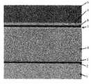
- FIG. 1shows a materials stack, under an embodiment.
- FIG. 2shows a cross-section of the materials stack over a portion of a pixel, under an embodiment.
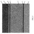
- FIG. 3shows a cross-section of the materials stack over a pixel, under an embodiment.
- the devicecomprises a first contact and a second contact, each having a work function, and an optically sensitive material between the first contact and the second contact.
- the optically sensitive materialcomprises a p-type semiconductor, and the optically sensitive material has a work function.
- the devicecomprises circuitry that applies a bias voltage between the first contact and the second contact.
- the magnitude of the work function of the optically sensitive materialis at least 0.4 eV greater than the magnitude of the work function of the first contact, and also at least 0.4 eV greater than the magnitude of the work function of the second contact.
- the optically sensitive materialhas an electron lifetime that is greater than the electron transit time from the first contact to the second contact when the bias is applied between the first contact and the second contact.
- the first contactprovides injection of electrons and blocking the extraction of holes.
- the interface between the first contact and the optically sensitive materialprovides a surface recombination velocity less than 1 cm/s.
- the devicecomprises a first contact, an n-type semiconductor, an optically sensitive material comprising a p-type semiconductor, and a second contact.
- the optically sensitive material and the second contacteach have a work function shallower than 4.5 ev.
- the devicecomprises circuitry that applies a bias voltage between the first contact and the second contact.
- the optically sensitive materialhas an electron lifetime that is greater than the electron transit time from the first contact to the second contact when the bias is applied between the first contact and the second contact.
- the first contactprovides injection of electrons and blocks the extraction of holes.
- the interface between the first contact and the optically sensitive materialprovides a surface recombination velocity less than 1 cm/s.
- the photodetectorcomprises a first contact and a second contact, each having a work function.
- the photodetectorcomprises an optically sensitive material between the first contact and the second contact, the optically sensitive material comprising a p-type semiconductor, and the optically sensitive material having a work function.
- the photodetectorcomprises circuitry that applies a bias voltage between the first contact and the second contact.
- the magnitude of the work function of the optically sensitive materialis at least 0.4 eV greater than the magnitude of the work function of the first contact, and also at least 0.4 eV greater than the magnitude of the work function of the second contact.
- the photodetectorcomprises circuitry that applies a bias voltage between the first contact and the second contact.
- the optically sensitive materialprovides a responsivity of at least 0.8 A/W when the bias is applied between the first contact and the second contact.
- Image sensorsincorporate arrays of photodetectors. These photodetectors sense light, converting it from an optical to an electronic signal. Following is a description of numerous features, any one or a combination of which can be found in the photodetectors of an embodiment; the embodiments herein are not, however, limited to only these features.
- the photodetectors of an embodimentare readily integrable with other circuitry related to the image sensing function, such as circuits which store charge, circuits which relay signal levels to the periphery of the array, circuits which manipulate these signal levels in the analog domain, circuits which convert analog into digital signals, and circuits which process image-related data in the digital domain.
- the photodetectors of an embodimentprovide a maximum of sensitivity to light within the wavelength band, or bands, of interest, along with low dark current. Sensitivity is often quantified using the measure signal-to-noise ratio (SNR) at a given level of illumination. Signal is maximized when the responsivity, quantum efficiency, or gain of the device is maximized. Noise is minimized when random fluctuations in electronic signals are minimized, subject to the limits prescribed by natural fluctuations in electrical currents and voltages at a given temperature. Relatedly, noise and other uncontrolled or difficult-to-predict variations in background signal are generally minimized when the magnitude of dark current is minimized.
- SNRsignal-to-noise ratio
- the photodetectors of an embodimentprovide a response time that is relatively fast when compared to conventional photodetectors formed using conventional processing methods.
- Applicationssuch as video imaging and shutterless still-image acquisition typically require photodetectors whose signal levels change substantially completely in response to a transient within fewer than 100 milliseconds (10 frames per second), or fewer than 33 milliseconds (30 frames per second), or even 1 millisecond ( 1/1000 second exposure of a still image).
- the photodetectors of an embodimentprovide for the detection of a wide range of light intensities in a manner that can conveniently be processed by conventional electronic circuitry. This feature is known as providing high dynamic range.
- One method of providing high dynamic rangeis to compress the measured electronic response as a function of the incident optical stimulus. Such compression can be referred to as a sublinear, i.e. a nonlinear with decreasing slope, dependence of electrical signal on incident intensity.
- High dynamic rangecan also be facilitated by employing a photodetector whose gain can be controlled, such as through the selection of a voltage bias known to produce a specific gain.
- the photodetectors of an embodimentcan provide for the discrimination among different spectral bands of electromagnetic radiation.
- spectral bands of electromagnetic radiationOf particular interest are the x-ray, ultraviolet, visible (including blue, green, and red), near-infrared, and short-wavelength infrared bands.
- Embodimentsinclude exchanging ligands passivating nanoparticle surfaces for shorter ligands that will provide for appropriate charge carrier mobilities once films are formed.
- Embodimentsinclude solution-phase exchanges which enable the realization of smooth-morphology films necessary to the realization of image sensors having acceptable consistent dark currents and photoresponses across an array.
- the photodetectors described hereinprovide relatively maximum sensitivity. They maximize signal by providing photoconductive gain. Values for photoconductive gain range from 1-50, resulting in responsivities in, for example, the visible wavelengths ranging from 0.4 A/W to 20 A/W.
- the photodetectors described hereinminimize noise by fusing nanocrystal cores such as to ensure substantially non-noise-degrading electrical communication among the particles making up the optically sensitive layer through which current flows.
- the photodetectors described hereinminimize dark current by minimizing the net doping of the active layer, thus ensuring that the dark carrier density, and thus the dark conductance, of these optically sensitive materials is minimized.
- the photodetectors described hereinminimize dark current by providing an electrode-to-nanocrystalline-layer electrical connection that blocks for example one type of carrier, including potentially the majority carrier at equilibrium.
- cross-linking moleculesare employed that utilize chemical functionalities that remove oxides, sulfates, and/or hydroxides responsible for p-type doping.
- a more intrinsic or even n-type optically sensitive layercan be provided, leading to lowered dark currents.
- many steps in quantum dot synthesis and/or processing and/or device packagingcan be performed in a controlled environment such as a Schlenk line or Glove Box; and optically sensitive layers can be encapsulated using substantially impermeable layers such as oxides, oxynitrides, or polymers such as polyxylylene, or epoxies, in order to prevent reactive gases such as oxygen or water from significantly permeating the optically sensitive layer.
- substantially impermeable layerssuch as oxides, oxynitrides, or polymers such as polyxylylene, or epoxies
- the photodetectors described hereinprovide a time-domain response that can be as rapid as approximately sub-100-milliseconds, sub-30-milliseconds, and sub-1-millisecond. In embodiments, this is achieved by providing gain-providing (and persistence-providing) trap states associated with the optically sensitive layer that trap at least one type of carrier for only a limited time period such as 100 milliseconds, 30 milliseconds, or sub-1 millisecond.
- PbS nanoparticlesare decorated with PbSO3, an oxide of PbS, which is shown to have a trap state lifetime in the vicinity of approximately 20-30 milliseconds, providing for a transient response suited to many video imaging applications.
- photodiodesare instead provided based on colloidal quantum dot layers, wherein two electrical contacts having appreciably different work functions are employed to contact the active layer.
- dark currentscan be minimized through operation of such devices without the application of an appreciable external voltage bias.
- cross-linking moietiessuch as benzenedithiol, a bidentate linker, can be employed to remove and/or passivate certain trap states that can be present, or can develop, in such materials.
- the photodetectors described hereinprovide enhanced dynamic range by producing a sublinear dependence of electrical signal (such as photocurrent).
- electrical signalsuch as photocurrent
- trap statesare available to become filled, and escape occurs following some moderate persistence, or trap state, lifetime, such as 30 milliseconds for example.
- trap state, lifetimesuch as 30 milliseconds for example.
- these trap statesbecome substantially filled, such that charge carriers experience shorter lifetimes, or persistence times, corresponding to lower differential gains.
- these devicesexhibit substantially constant gains over a range of low to middling intensities, followed by a gentle roll-off in gain at higher intensities.
- photocurrentdepends approximately linearly on intensity, but at higher intensities, photocurrent exhibits sublinear dependence on intensity.
- photodetectorsare provided wherein photoconductive gain depends on the bias applied to a device. This arises because gain is proportional to carrier lifetime divided by carrier transit time, and transit time varies in inverse proportionality with applied field. In embodiments, circuits are developed that exploit this dependence of gain on bias to increase dynamic range.
- photodetectors described hereinare readily altered, or ‘tuned’, to provide sensitivity to different spectral bands. Tuning is provided herein through the quantum size effect, whereby nanoparticle diameter is decreased, in cases through synthetic control, to increase the effective bandgap of the resulting quantum dots. Another method of tuning is provided through the choice of materials composition, wherein the use of a material having a larger bulk bandgap generally facilitates the realization of a photodetector with responsivity onset at a relatively higher photon energy.
- photodetectors having different absorption onsetscan be superimposed to form vertical pixels, wherein pixel(s) closer to the source of optical signal absorb and sense higher-energy bands of electromagnetic radiation, whereas pixel(s) further from the source of optical signal absorb and sense lower-energy bands.
- FIG. 1shows a materials stack, under an embodiment.
- the materials stackis integrated with complementary metal-oxide-semiconductor (CMOS) silicon circuitry, but is not so limited.
- CMOScomplementary metal-oxide-semiconductor
- the use of CMOS silicon circuitry to read the signals transduced by photoconductive photodetectors, including top-surface photodetectors, and including those based on colloidal quantum dots including PbS,includes the integration of top-surface photoconductive materials with silicon CMOS electronics. The structure and composition of the photoconductive photodetector is described in detail below.
- FIG. 2shows a cross-section of the materials stack over a portion of a pixel, under an embodiment.
- the figuredepicts, in the left and right hand sides or regions, the same materials stack referenced in FIG. 1 .
- a discontinuity in the material metal ‘ 1 ’which is replaced by material ‘ 7 .
- Material ‘ 7 ’can in general be an insulator such as SiO2 or SiOxNy.
- Embodiments of FIG. 2can be referred as a portion of a lateral pixel.
- currentsubstantially flows between metals ‘ 1 ’ through material ‘ 2 ’ (interface), material ‘ 3 ’ (adhesion), and material ‘ 4 ’ (photosensitive layer).
- Different portions or regions of the materials stack described hereinare referred to herein as “materials” or “layers” but are not so limited.
- FIG. 3shows a cross-section of the materials stack over a pixel, under an embodiment. Embodiments of FIG. 3 can be referred to as a portion of a vertical pixel.
- An interface material or layer ‘ 8 ’is incorporated or integrated on a top portion or region of the device.
- Material ‘ 8 ’comprises a member or members of the sets of materials described herein as material ‘ 2 ’.
- a metal or contact layer or material ‘ 9 ’is incorporated or integrated on a top portion or region of the device.
- the metal or contact layer ‘ 9 ’comprises a member or members of the sets of materials described herein as material ‘ 1 ’.
- material ‘ 9 ’comprises a transparent conductive material such as indium tin oxide, tin oxide, or a thin (substantially nonabsorbing to visible light) metal such as TiN, Al, TaN, or other metals recited below under material ‘ 1 .’
- Material ‘ 1 ’is a metal that lies above the substrate (not shown) and can be a silicon CMOS integrated circuit. During processing it can be a 200 mm or 300 mm wafer, i.e. a wafer that has not yet been singulated to form die.
- Material ‘ 1 ’refers to a metal, present at the top surface of the CMOS integrated circuit wafer, which is presented and available for physical, chemical, and electrical connection with subsequent layers.
- the metalcan include: TiN, TiO2, TixNy, Al, Au, Pt, Ni, Pd, ITO, Cu, Ru, TiSi, WSi2, and combinations thereof.
- Material ‘ 1 ’is referred to as the contact, or the electrode, although it shall be discussed herein that the behaviour of this contact is influenced by thin layers that can reside between the metal and material ‘ 4 ’, the photoconductive quantum dot layer.
- the metalcan be chosen to achieve a particular work function, and can influence whether an ohmic or non-ohmic (e.g. Schottky) contact is formed with respect to the layers to which it is proximate.
- the metalcan be chosen to provide a shallow work function, such as a value generally between ⁇ 2.0 eV and ⁇ 4.5 eV, for example values lying between ⁇ 2.0 eV and ⁇ 4.2 eV.
- the metalcan achieve a surface roughness less than 5 nm root-mean-squared.
- the metalcan be patterned with a critical dimension of 0.18 micrometers or smaller.
- the metalcan be patterned such that, pixel-to-pixel, the spacing of the electrodes (such as between a pixel center electrode and a grid) does not vary by more than a standard deviation of 1%.
- the metalcan be terminated with an oxide such as a native oxide—such as TiOxNy in the case of TiN.
- oxidesuch as TiOxNy in the case of TiN.
- this oxide, or other materials atop itsuch as organic residues, inorganic residues such as ‘polymer,’ etc. are of a consistent and known composition thickness.
- the metalcan be a conductive material, where the bulk of the material constituting the metal can have a resistivity that is less than 100 microOhm*cm.
- the metalcan be processed such that, across the wafer, in all regions where light-sensing pixels are to be formed, it is not capped with any additional oxides or organics or contaminants.
- the top surface of the wafer, prior to or after the formation of the interface layer,can comprise regions of metal and insulating material (such as an insulating oxide), such that the peak-to-valley distance of features on this surface is less than 50 nm.
- metal and insulating materialsuch as an insulating oxide
- the leakage current flowing between a pixel electrode in the center of a 1.1 ⁇ 1.1 um or 1.4 ⁇ 1.4 um square grid electrideshould be less than 0.1 fA at 3 V bias.
- Layers or materials above material ‘ 1 ’form an interface, or interface layer.
- Each of the layers forming the interfaceis described in detail below, in turn.
- Material “ 2 ”is the first part or portion of the interface layer, and comprises a material that resides atop the metal.
- Material ‘ 2 ’can comprise a pure, clean surface of the metal.
- the material of this layercan include oxides, including those generally formed, either through exposure to water, oxygen, or other oxidizing species, as a result of the presence of the exposed metal; or it can be deliberately formed such as through exposure to a controlled oxidizing environment and exposures to elevated temperatures, such as in rapid thermal processing.
- Native oxidesinclude, for example, the following: TiO2 and TiOxNy atop TiN; Al2O3 atop Al; Au2O3 atop Au; PtO or PtO2 on Pt; Ni2O3 atop Ni; WO3 atop W; PdO atop Pd; and oxygen-rich ITO atop ITO. It can be that such a native oxide is to be removed, such as using etching, and replaced with another layer. For example, a native oxide such as TiOxNy can be etched (using a process such as argon sputtering) and then a layer can be deposited on top of it such as a controlled oxide such as TiO2, TiOx, or TiOxNy. The sum of the thicknesses of native oxides and deliberately-deposited oxides can be between 2 and 20 nm.
- a portion of material ‘ 2 ’can be a material that is substantially transparent to most or all wavelengths of visible light. It can have a bandgap that is larger than 2 eV or larger than 2.5 eV or larger than 3 eV. It can be a large-bandgap doped semiconductor. It can achieve doping through stoichiometry, such as in the case of TiOx where x is varied below or above material 2 in order to achieve net doping. Values of x can be typically 1.9 to achieve an excess of Ti over stoichiometric TiO2. Values of x can typically be 2.1 to achieve an excess of O over stoichiometric TiO2.
- TiOx where x ⁇ ⁇ 2can be achieved by exposing stoichiometric TiO2 to a reducing environment.
- the density of free electronscan be increased, corresponding to greater n-type doping, by increase the extent to which initially stoichiometric TiO2 is reduced, i.e. by decreasing x in TiOx more considerably relative to the value 2.
- TiO2can be doped with nitrogen in order to modify its free carrier concentration, work function, and electron affinity.
- TiO2 or TiOxcan be doped with B, C, Co, Fe. It can be a mildly n-type material such as lightly doped TiOx having an equilibrium carrier density of 10 ⁇ 10 cm-3.
- Itcan be a moderately doped n-type material such as TiOx having an equilibrium carrier density of 10 ⁇ 16 cm-3. It can be a more strongly doped n-type material such as TiOx having an equilibrium carrier density of 10 ⁇ 18 or 10 ⁇ 19 cm-3. Its electron affinity can correspond energetically substantially closely with the work function of the metal. Its work function can correspond substantially closely with the work function of the metal. Its ionization potential can reside at an energy that is much deeper than the ionization potential of the optically-absorbing layer (material ‘ 4 ’ described herein).
- Material ‘ 3 ’can also be present in the interface layer, and comprises a material that can be positioned or reside atop the first portion of the interface layer.
- Material ‘ 3 ’includes adsorbed organics such as organic molecules, introduced deliberate or accidentally or through some combination thereof, that reside above the metal, either in direct contact with the metal, or in direct contact with the metal oxide. These molecules are discussed in detail herein.
- Embodimentsinclude material ‘ 2 ’ while material ‘ 3 ’ is absent. Such embodiments include choices of materials in which no adhesion layer such as that provided by material ‘ 3 ’ is required. As an example, if material ‘ 2 ’ incorporates a metal such as titanium, such as if material ‘ 2 ’ incorporates TiOx, and if material ‘ 4 ’ incorporates a crosslinker such as mercaptobenzoic acid, in which one functional group on the mercaptobenzoic acid binds the TiOx, then adhesion between material ‘ 4 ’ and material ‘ 2 ’ can be provided without explicit inclusion of material ‘ 3 ’.
- all of material ‘ 1 ’ material ‘ 2 ’ and material ‘ 3 ’can be present.
- Embodimentsinclude cases where a heterojunction is formed via the use of a large-bandgap oxide in material ‘ 2 ’ to the photosensitive layer ‘ 4 .’
- Embodimentsinclude a device in which TiN or TiOxNy forms the metal ‘ 1 ,’ layer ‘ 2 ’ includes a large-bandgap semiconductor such as TiOx (which can be structurally doped, impurity doped, both, or neither), and an adhesion layer such as hexamethyldisilazane can be provided in material ‘ 3 ’.
- material ‘ 1 ’can be aluminum metal
- material ‘ 2 ’can include a native oxide of aluminum and can include a doped conductive oxide such as doped Al2O3 and/or can include a large-bandgap semiconductor such as TiOx (which can be structurally doped, impurity doped, both, or neither)
- material ‘ 3 ’can include an adhesion layer such as hexamethyldisilazane can be provided in material ‘ 3 ’.
- material ‘ 1 ’can include aluminum, gallium, indium, tin, lead, bismuth, magnesium, calcium, zinc, molybdenum, titanium, vanadium, lanthanum, chromium, manganese, iron, cobalt, nickel, copper, zirconium, niobium, palladium, silver, hafnium, tantalum, tungsten, iridium, platinum, gold.
- metals used in standard CMOSsuch as aluminum, tungsten, tantalum, titanium, copper can be preferred.
- material ‘ 2 ’can include a surface of the metal and can include oxides, nitrides, or oxynitrides of aluminum, gallium, indium, tin, lead, bismuth, magnesium, calcium, zinc, molybdenum, titanium, vanadium, lanthanum, chromium, manganese, iron, cobalt, nickel, copper, zirconium, niobium, palladium, silver, hafnium, tantalum, tungsten, iridium, platinum, gold.
- itcan be preferred that it include oxides, nitrides, or oxynitrides of metals used in standard CMOS such as aluminum, tungsten, tantalum, titanium, copper.
- material ‘ 2 ’can comprise multiple sublayers.
- itcan comprise a sublayer consisting of a metal such as aluminum, gallium, indium, tin, lead, bismuth, magnesium, calcium, zinc, molybdenum, titanium, vanadium, lanthanum, chromium, manganese, iron, cobalt, nickel, copper, zirconium, niobium, palladium, silver, hafnium, tantalum, tungsten, iridium, platinum, gold.
- this sublayercan comprise metals used in standard CMOS such as aluminum, tungsten, tantalum, titanium, copper.
- material ‘ 2 ’can comprise a further sublayer consisting of oxides, nitrides, or oxynitrides of aluminum, gallium, indium, tin, lead, bismuth, magnesium, calcium, zinc, molybdenum, titanium, vanadium, lanthanum, chromium, manganese, iron, cobalt, nickel, copper, zirconium, niobium, palladium, silver, hafnium, tantalum, tungsten, iridium, platinum, gold.
- this further sublayerinclude oxides, nitrides, or oxynitrides of metals used in standard CMOS such as aluminum, tungsten, tantalum, titanium, copper.
- the layer referred to as material ‘ 4 ’refers to an optically-absorbing layer that includes nanocrystals, or quantum dots.
- a quantum dot (QD), depicted in ‘ 1220 ’ in FIG. 1can be a nanostructure, for example a semiconductor nanostructure, that confines a conduction band electrons, valence band holes, or excitons (bound pairs of conduction band electrons and valence band holes) in all three spatial directions. The confinement can be due to electrostatic potentials (e.g., generated by external electrodes, doping, strain, impurities), the presence of an interface between different semiconductor materials (e.g., in core-shell nanocrystal systems, incorporated in ‘ 1221 ’ of FIG.
- a quantum dotexhibits in its absorption spectrum the effects of the discrete quantized energy spectrum of an idealized zero-dimensional system.
- the wave functions that correspond to this discrete energy spectrumare substantially spatially localized within the quantum dot, but extend over many periods of the crystal lattice of the material.
- the QDcan have a core of a semiconductor or compound semiconductor material, such as PbS.
- Ligandscan be attached to some or all of the outer surface or can be removed in some embodiments.
- the cores of adjacent QDscan be fused together to form a continuous film of nanocrystal material with nanoscale features.
- corescan be connected to one another by linker molecules.
- trap statescan be formed on the outer surface of the nanocrystal material.
- the corecan be PbS and trap states can be formed by an oxide such as PbSO3 formed on the outer surface of core.
- a QD layercan include a continuous network of fused QD cores, having outer surfaces that are of a different composition than that in the core, e.g., oxidized core material such as PbS03, or a different kind of semiconductor.
- the individual QD cores in the filmare in intimate contact, but continue to exhibit many of the properties of individual quantum dots.
- a lone (unfused) quantum dothas a well-characterized excitonic absorbance wavelength peak that arises from quantum effects related to its size, e.g., 1-10 nm.
- the excitonic absorbance wavelength peak of the fused QDs in the filmis not significantly shifted from the central absorbance wavelength that was present prior to fusing.
- the central absorbance wavelengthcan change by about 10% or less when fused.
- the QDs in the filmretain their quantum effects, despite the fact that they can be an integral part of a macroscopic structure.
- QD coresare linked by linker molecules as described further below. This allows current to flow more readily than through unlinked, unfused QDs.
- linker moleculesto form a continuous film of QDs instead of fusing the cores can reduce the dark current for some photoconductor and image sensor embodiments.
- the QD layeris exceptionally radiation sensitive. This sensitivity is particularly useful for low-radiation imaging applications.
- the gain of the devicecan be dynamically adjusted so that the QDPC saturates, that is, additional photons continue to provide additional useful information that can be discerned by the read-out electronic circuit. Tuning of gain can be conveniently achieved by changing the voltage bias, and thus the resultant electric field, across a given device, e.g., a pixel.
- Some embodiments of QD devicesinclude a QD layer and a custom-designed or pre-fabricated electronic read-out integrated circuit. The QD layer is then formed directly onto the custom-designed or pre-fabricated electronic read-out integrated circuit. The QD layer can additionally be patterned so that it forms individual islands.
- the QD layerwherever the QD layer overlies the circuit, it continuously overlaps and contacts at least some of the features of the circuit. In some embodiments, if the QD layer overlies three-dimensional features of the circuit, the QD layer can conform to these features. In other words, there exists a substantially contiguous interface between the QD layer and the underlying electronic read-out integrated circuit.
- One or more electrodes in the circuitcontact the QD layer and are capable of relaying information about the QD layer, e.g., an electronic signal related to the amount of radiation on the QD layer, to a readout circuit.
- the QD layercan be provided in a continuous manner to cover the entire underlying circuit, such as a readout circuit, or patterned.
- the fill factorcan approach about 100%, with patterning, the fill factor is reduced, but can still be much greater than a typical 35% for some example CMOS sensors that use silicon photodiodes.
- the QD optical devicesare readily fabricated using techniques available in a facility normally used to make conventional CMOS devices. For example, a layer of QDs can be solution-coated onto a pre-fabricated electronic read-out circuit using, e.g., spin-coating, which is a standard CMOS process, and optionally further processed with other CMOS-compatible techniques to provide the final QD layer for use in the device. Because the QD layer need not require exotic or difficult techniques to fabricate, but can instead be made using standard CMOS processes, the QD optical devices can be made in high volumes, and with no significant increase in capital cost (other than materials) over current CMOS process steps.
- the QD materialcan have an absorption cutoff approximately at the edge of the visible, such as round 650 nm.
- the QD materialcan have an absorption cutoff at longer wavelengths, in order to ensure a high absorbance over the entire visible, such as when the absorption cutoff is in the 700-900 nm range.
- the QD filmcan be deposited using conventional spin-on process, ink-jet printing process, Langmuir-Blodgett film deposition, electrokinetic sprays, or nano-imprint.
- the QD filmcan be deposited using dispensing of QD solution on a wafer at 30 RPM followed by three-step spin process.
- the spectral position of the peak in the QD solution absorptioncan be specified to lie at 740 nm, +/ ⁇ 10 nm.
- the ratio of the absorbance at the QD absorption peak near 740 nm, and the valley slightly to the blue of this peak,can be specified to be 1.2.
- the thickness of the quantum dot layercan be specified to be 300 nm+/ ⁇ 50 nm.
- the thickness of the quantum dot layercan be chosen to ensure that, over the spectral range 400-640 nm, greater than 90% of all light incident on the film is absorbed.
- the roughness (root-mean-squared) of the quantum dot filmcan be specified to be less than 5 nm.
- the dark current in a 1.1 ⁇ 1.1 um pixelcan be less than 0.5 fA under suitable bias, such as a 3V bias.
- the gaincan be greater than 10 in a 1.1 ⁇ 1.1 um pixel.
- Alklali metal impuritiescan be present at lower than 5 E17 cm-3 concentration in the quantum dot film. Defects greater than 0.16 microns in size can be fewer than 20 across a 200 mm wafer.
- the mobility of the flowing carriercan exceed 1 E-5 cm2/Vs.
- the loading fraction of nanocrystals in the filmcan exceed 30% by volume.
- Incorporated into material ‘ 4 ’can be chemical species such as PbO, PbSO4, PbSO3, poly-sulfates; and they can also include physically-adsorbed species such as O2, N2, Ar, H2, CO2, H2O, and H2S.
- Incorporated into material ‘ 4 ’can be molecules that are bound to the surface of at least one nanoparticle, or nanocrystal, or quantum dot. These can include thiol-terminated ligands such as benzenethiol, ethanethiol; carboxylate-terminated molecules such as oleic acid and formic acid; amine-terminated ligands such as pyridine, butylamine, octylamine. They can also include bidentate crosslinkers such as benzenedithiol, ethanedithiol, and butanedithiol.
- thiol-terminated ligandssuch as benzenethiol, ethanethiol
- carboxylate-terminated moleculessuch as oleic acid and formic acid
- amine-terminated ligandssuch as pyridine, butylamine, octylamine.
- bidentate crosslinkerssuch as benzenedithiol, e
- multidentate moleculesthat include (1) a backbone (2) certain sidegroups and/or endgroups that bind to the nanoparticle surface, including thiols, amines, carboxylates; and (3) other functional groups such as those that confer solubility in polar, nonpolar, and partially polar solvents.
- Material ‘ 5 ’can include layers on top of ‘ 4 ’ that can provide passivation of the underlying material, including minimizing the extent of movement of species between layers ‘ 1 ’-‘ 4 ’ of the materials stack and the outside of the materials stack. This layer can also facilitate good physical adhesion with overlying layers such as encapsulant layers.
- Material ‘ 6 ’refers to a layer, or layers, that can be included on top of the material stack and can serve to minimize the extent of movement of species between layers ‘ 1 ’-‘ 4 ’ of the materials stack and the outside of the materials stack.
- the quantum dot film layercan be encapsulated against oxygen and moisture diffusion using a low-temperature (less than 100° C.) PECVD SiO2, SiN, or SiOCN process providing optically transparent film suitable for further integration with CFA.
- the filmcan be specified to have a thickness of 200 nm+/ ⁇ 10 nm. It can be specified to have a surface roughness less than 5 nm rms. Optical transmittance can exceed 99%.
- Adhesioncan be provided to the underlying layers.
- An embodimentcan have fewer than twenty greater-than-0.1-um particle defects across a 200 mm wafer.
- An embodimentcan have fewer than twenty greater-than-0.1-um pinholes across a 200 mm wafer.
- the nature of the interface between the electrical contact and the light-sensitive semiconductoris an important determinant of device stability and performance. For example, whether the contact is ohmic vs. Schottky, and whether the contact and semiconductor are separated by a thin interfacial layer which passivates at least one of the ⁇ semiconductor and the contact ⁇ , are important in stability and performance.
- the composition of the photoconductive layeris an important determinant of device performance and stability.
- photoconductive materialsare often sensitive to the presence of physisorbed or chemisorbed species, possibly originally presented as a gas (such as O2, H2O, CO2), on the nanoparticle surfaces—these must thus be carefully controlled during processing, and an encapsulating and/or passivating layer(s) can be used, above and/or below, the photoconductive layer, to preserve consistent photoconductive features over time. Further description follows of the interface between metal and semiconductor of an embodiment as well as encapsulation of an embodiment.
- the layer ‘ 4 ’can be made from silicon, including single-crystal silicon, polycrystalline silicon, nanocrystalline silicon, or amorphous silicon including hydrogenated amorphous silicon.
- the layer ‘ 4 ’can include materials that are not substantially quantum-confined, but instead substantially retain the bandgap of a bulk semiconductor.
- Embodimentsinclude crystalline or polycrystalline or nanocrystalline or amorphous embodiments of materials such as silicon, gallium arsenide, carbon, PbS, PbSe, PbTe, Bi2S3, In2S3, Copper-Indium-Gallium-Selenide (or Sulfide), SnS, SnSe, SnTe, in which the characteristic size of any crystalline or partially-crystalline subunits is typically not smaller than the Bohr exciton radius (the characteristic spatial extent of electron-hold pairs) in the semiconductor material employed.
- the interface formation of an embodimentcan comprise the cleaning and termination of material ‘ 1 ’.
- the interface of an embodimentcan comprise an oxide formed on material ‘ 1 ’, including a native oxide as a part of material ‘ 2 ’.
- the thickness of this oxideis an important determinant of device performance. Excessive oxide thicknesses (e.g., thickness exceeding 10-20 nm) can provide an excessive contact resistance in series with the photoconductive film, necessitating the application of an undesirably increased bias c/o the biasing circuit. In embodiments, the thickness of this native oxide is kept in the range of less than 5 nm.
- the interface of an embodimentcan comprise a further thin layer as part of material ‘ 2 ’, such as TiO2, generally included to modify the work function of the interface with the semiconductor to be placed on top.
- This layercan, in embodiments, provide selectivity in favour of one type of charge carrier: for example, TiO2 can be configured such that, at the operating bias, it efficiently injects electrons into the conduction band of the photoconductive semiconducting layer; but, at this same bias, it withdraws holes from the valence band of the photoconductive semiconducting layer with much lower effectiveness.
- TiO2can be configured such that, at the operating bias, it efficiently extracts electrons from the conduction band of the photoconductive semiconducting layer; but, at this same bias, it injects holes into the valence band of the photoconductive semiconducting layer with much lower effectiveness.
- the interface of an embodimentcan comprise a further thin layer as part of material ‘ 2 ’, such as MEH-PPV, generally included to enable the flow of one type of charge carriers, such as holes, while blocking the flow of the other type, such as electrons.
- material ‘ 2 ’such as MEH-PPV
- the interface of an embodimentcan comprise a thin layer as part of material ‘ 3 ’, possibly a self-organized molecular monolayer, designed to anchor on one side of the molecules to the underlying layers, and at the other terminus of the molecule to anchor to the semiconductor to be placed atop, with the goal of ensuring controlled electronic communication, and also ensuring mechanical stability, e.g., good adhesion between the materials making up the multilayer device.
- the layered structure of an embodimentprovides efficient charge carrier transfer through an interface.
- the layered structurecan form a substantially ohmic contact with the photoconductive semiconductor layer, providing for little or no depletion of the semiconductor near the interface, and providing for efficient injection and extraction of at least one type (e.g. electrons, holes) of charge carrier.
- the layered structurecan form a Schottky contact with the photoconductive semiconductor layer, providing an energetic barrier that must be overcome for charge carriers to be injected and/or withdrawn.
- the layered structurecan form a selective contact, providing considerably more efficient injection of one type of charge carrier (e.g. electrons) than it provides extraction of the other type (e.g. holes); and/or providing considerably more efficient withdrawal of one type of charge carrier (e.g. electrons) than it provides injection of the other type (e.g. holes).
- the layered structure of an embodimentprovides a work function of the contact surface where the effective workfunction is determined by the material of the electrode, material of the interfacial layer, and its thickness.
- the layered structure of an embodimentprovides blocking capability to suppress the undesirable carrier transfer, for example as a layer proving electron trap states on the surface of metal electrode in case of p-semiconductor photodetector device.
- the layered structure of an embodimentprovides strong bonding of the photosensitive semiconductor material to the metal electrode.
- the layered structure of an embodimentprovides high temperature stability of the metal electrode-semiconductor material interface.
- the structure and composition of electronic devices of an embodiment with an engineered interfacial layerincludes but is not limited to a metal electrode comprising a conventional material used in semiconductor manufacturing being either readily oxidized, or nitridized, or both in a chosen stoichiometric combination, such as Ti, W, Ta, Hf, Al, Cu, Cr, Ag; or being resistive to oxidation or nitridization such as Au, Pt, Rh, Ir, Ru, graphite, amorphous carbon, graphene, or carbon nanotubes.
- These metal electrodescan also be formed from alloys, conductive glasses, and various conductive intermetallics. The work function of the resultant electrodes can be tuned through exposure to oxygen, nitrogen, or a combination thereof at a specific temperature for a specific time.
- the structure and composition of electronic devices of an embodimentincludes an interfacial layer on the surface of the metal contact.
- the interfacial layer of an embodimentincludes an oxide or intermetallic of the element of the electrode with the maximum thickness sufficient to keep the ohmic characteristics of the contact but with the minimum thickness sufficient to create electron trap states.
- the structurecan be created or generated using PVD (physical vapor deposition), ALD (atomic layer deposition), CVD (chemical vapor deposition), ion cluster, ion beam deposition, ion implantation, anneal or other this film deposition method.
- Such filmscan be formed from aqueous and non-aqueous liquid formulations, which can include electrochemical techniques, to form hydroxides, oxides, fluorides, sulfides, sulfates, sulfites, sulphonates, phosphates, phosphonates, phosphides, nitrates, nitrites, nitrides, carbonates, carbides, and other types of salts or complexes of the said metals.
- the average thickness of the interfacial layercan vary from a 0.1 nm-0.2 nm to 10 nm-50 nm depending on conductivity of the final interfacial layer, and work function of the metal electrode itself.
- the interfacial layer of an embodimentincludes another oxide deposited on the surface of the electrode, said oxide been doped TiO2, HfO2, Al2O3, SiO2, Ta2O5, Zn x Al y O, Zn x Ga y O, ZnIn x Sn y O, and similar p-conductive materials. Again, these materials can be deposited using the methods mentioned earlier.
- interfacial layerAdditional properties of the interfacial layer are determined by the necessity to form relatively strong chemical bond, preferably covalent, to the components of the semiconductor photosensitive layer.
- the surface of the interfacial layeris modified using organic by-functional molecules, where one type of functional group provides selective bonding to the interfacial layer surface, while the second type of functional groups provides bonding to either ligand or directly to semiconductor nanocrystals.
- These bonding moleculescan be formed on non-conductive alkane or aryl backbone or can be formed on conductive backbone including aniline, acetylene, or other types of sp2 hybridzed carbon.
- the functional groups to provide bonding to the oxidized surface of the electrode or surface of the interfacial layerinclude but are not limited to silanes, siloxanes, silizanes, primary, secondary, or tertiary amines, imides, phosphates, oximes, carboxylates.
- the average length of the organic molecule forming the interfacial layercan typically vary from 2 to 16 carbon atoms.
- the interfacial layercan be formed from a molecule including two similar functional groups providing bonding directly to the metal surface on one side and to a nanocrystal on another side.
- An examplewould be formation of Au—S—R—S—NC bond.
- thickness and conductivity of the organic interfacial layerdefined by the required electronic device properties.
- the continuous filmcan be patterned using conventional patterning techniques.
- one of the electrodescan be made of a metal with one work function while another electrode can made having a different workfunction and/or type of conductivity (electron or hole).
- the same approach as aboveis used for the bottom electrode while the interfacial layer on top is formed by deposition of organic molecules or a thin transparent layer of the semiconductor material.
- Molecules described aboveare polymers with the degree of polymerization from approximately 1 through approximately 10,000.
- the devicecan be formed to include a consistent, reliable combination of material ‘ 1 ’ and material ‘ 2 ’ which can be followed by the controlled formation or material ‘ 3 ’ and the optically-absorbing layer ‘ 4 ’.
- an embodimentcan provide through material ‘ 1 ’ a highly conductive contact having resistivity less than 100 microohm*cm and a work function lying between ⁇ 2 eV and ⁇ 4.5 V and lying between ⁇ 2 eV and ⁇ 4.2 eV.
- An embodimentcan provide through material ‘ 2 ’ a large-bandgap layer that permits the injection of electrons into the ensuing photosensitive semiconductor layer, but blocks the extraction of holes from this layer.
- An embodimentcan achieve a controlled thickness of a doped substantially transparent oxide, such as n-type TiOx, as part of the first part of material ‘ 2 ’.
- a TiOx thicknessin the range 2-20 which is controlled to within 1-5 nm; and where the TiOx has a specifically-chosen carrier density of 1 ⁇ 1018 cm-3 with a tight band of control such as +/ ⁇ 10% in carrier density.
- Manufacturing of a stack or configuration of layers of the device described hereincan comprise: (1) formation of the metal, such as via the sputtering of titanium in a nitrogen atmosphere, resulting in the formation of TiN; (2) subsequent processing that results in the formation of an interface layer such as a native oxide, such as TiOxNy or TiOx (it can be that this subsequent processing results in range of possible oxide thicknesses and dopings and carrier concentrations); (3) removal of the native oxide layer through an etch such as a sulfuric acid—hydrogen peroxide—deionized water etch, or an ammonium peroxide etch, or a physical etch such as argon sputtering, or a reactive sputter etch such as argon and hydrogen; in an embodiment this etch completely removes the oxide; a modest overetch to ensure complete removal can be implemented; (4) an embodiment deposits a controlled thickness, controlled doping, and controlled-surface-terminated layer of an oxide such as TiOx, TiOxNy, or other interface layer.
- Methodssuch as physical vapour deposition (including DC sputtering, RF sputtering, of a TiOx source, a TiN source, or a Ti source, in the presence of O2, N2, or a combination thereof) can be employed to deposit these layers.
- Methodsalso include CVD and ALD where a precursor is first deposited on the surface of the wafer, and a reaction proceeds at a controlled temperature. In cases where TiOx is to be formed, precursors can be employed.
- Manufacturing of a stack or configuration of layers of the device described hereincan comprise: (1) Formation of the metal, such as via the sputtering of titanium in a nitrogen atmosphere, resulting in the formation of TiN; (2) In-situ transitioning to the deposition on top of this metal of an interface layer.
- Thesecan include TiOx or TiOxNy.
- This layercan possess a controlled thickness, controlled doping, and controlled-surface-terminated layer of an oxide such as TiOx, TiOxNy, or other interface layer.
- Methodssuch as physical vapour deposition (including DC sputtering, RF sputtering, of a TiOx source, a TiN source, or a Ti source, in the presence of O2, N2, or a combination thereof) can be employed to deposit these layers.
- Methodsalso include CVD and ALD where a precursor is first deposited on the surface of the wafer, and a reaction proceeds at a controlled temperature.
- CVD and ALDwhere a precursor is first deposited on the surface of the wafer, and a reaction proceeds at a controlled temperature.
- chemical precursorscan be employed.
- an encapsulating and/or passivating layer(s)can be used, above and/or below, the photoconductive layer, to preserve consistent photoconductive features over time.
- the embodiments described hereinensure a consistent gas environment (or lack of significant presence of a gas) in the photoconductive layer.
- a gas environmentor lack of significant presence of a gas
- vacuum, Argon, Nitrogen, Oxygen, Hydrogen, Carbon Dioxidecan be included or excluded, in various proportions and to various degrees.
- Embodimentscan exclude Oxygen, H2O, CO2, and include only either the absence of gas molecules, or nonreactive materials such as Argon and/or Nitrogen.
- an encapsulant layercan be included whose purpose is to avoid gas exchange between the photoconductive film and the region exterior to this film.
- Materials employed in an embodiment for this purposeinclude but are not limited to: polyxylylene; As2S3 or As2Se3; Si3N4, SiO2, and mixtures thereof ie SiOxNy; oxides such as TiO2, HfO2, Al2O3, SiO2, Ta2O5, ZnxAlyO, ZnxGayO, ZnInxSny.
- the encapsulant materialcan be preceded by a passivation layer, potentially in the form of a substantially single molecular monolayer.
- This first layercan serve to protect the encapsulated structure during the deposition of the encapsulant: for example, a layer of a material such as polyxylylene can first be deposited, using a procedure that does not deleteriously alter the optoelectronic behaviour of the photoconductive layer, and providing protection of the photoconductive layer during ensuing encapsulation processes. It can, for example, protect the film from reactions resultant from oxygen and its radicals that are present during certain processes employed in the deposition of oxygen-containing encapsulants such as SiOx, SiOxNy, etc.
- typical thicknesses of the total encapsulant stackcan range from a single monolayer (typically ⁇ nm or slightly sub-nm e.g. 5 A) to typically 1 micrometer. In embodiments, typical thicknesses of the total encapsulant stack can be desired to be less than 1-2 micrometers in order to perturb minimally the optical properties of the array.
- included in at least one of the layers ‘ 1 ’ ‘ 2 ’ ‘ 3 ’ ‘ 4 ’ ‘ 5 ’can be materials that serve to getter molecules that could react with materials in the device, including materials which, if reacted, could alter the photoelectrical properties of the device.
- reactive molecules that could enter the deviceinclude O2 and H2O and O3.
- materials in the device that could have their photoelectrical properties altered by such reactionsinclude material ‘ 4 ’ NC, material ‘ 3 ’ adhesion, material ‘ 2 ’ interface, and ‘ 1 ’ metal.
- gettering moietiesinclude borazons, borohydrides including tetrahydroborates, catecholborane, L-selectride, lithium borohydride, lithium triethylborohydride, sodium borohydride, and uranium borohydride.
- gettering moietiesinclude hydrolysable siloxanes.
- the devices of an embodimentcan include a strong chemical bond (e.g., covalent), to the components of the semiconductor photosensitive layer.
- a strong chemical bonde.g., covalent
- the surface of the interfacial layeris modified using organic by-functional molecules, where one type of functional group provides selective bonding to the interfacial layer surface, while the second type of functional group provides bonding to either ligand or directly to semiconductor nanocrystals.
- These bonding moleculescan be formed on non-conductive alkane or aryl backbone or can be formed on conductive backbone including aniline, acetylene, or other types of sp2 hybridized carbon.
- the functional groups to provide bonding to the oxidecan include silanes, siloxanes, silizanes, primary, secondary, or tertiary amines, imides, phosphates, oximes, carboxylates.
- Manufacturing processes of the devices of an embodimentcan include a wafer pre-clean using SC1 of 30 second duration and at 20° C. in a clean dry air ambient. Manufacturing processes of the devices of an embodiment can include a rinse in de-ionized water of 30 second duration at 20° C. in a clean dry air ambient. Manufacturing processes of the devices of an embodiment can include drying the wafer involving a bake for a prescribed period of time (such as 30 seconds-24 hours) at a prescribed temperature (such as 20, 70, 150, or 200 degrees C.) in a prescribed environment (such as clean dry air, vacuum, nitrogen, argon, or a reducing atmosphere such as hydrogen, or a controlled oxidizing atmosphere containing an inert gas such as N2 or Ar and an oxidizing gas such as O2).
- a bake for a prescribed period of timesuch as 30 seconds-24 hours
- a prescribed temperaturesuch as 20, 70, 150, or 200 degrees C.
- a prescribed environmentsuch as clean dry air, vacuum, nitrogen, argon, or a reducing atmosphere such as hydrogen
- Manufacturing processes of the devices of an embodimentcan include the stipulation of maximum and minimum and average queue times in between other processes.
- Manufacturing processes of the devices of an embodimentcan include treatments of substrates and quantum dot films including exposure to ethanedithiol in acetonitrile at a prescribed temperature, such as 25 degrees C., for a prescribed time, such as 20 seconds, in a prescribed atmosphere, such as N2.
- Manufacturing processes of the devices of an embodimentcan include treatments of substrates and quantum dot films including exposure to hexanedithiol in acetonitrile at a prescribed temperature, such as 25 degrees C., for a prescribed time, such as 20 seconds, in a prescribed atmosphere, such as N2.
- Manufacturing processes of the devices of an embodimentcan include the deposition of a dielectric capping layer, such as SiO2, at or beneath a certain temperature, such as 100° C., and to a specified thickness of dielectric capping layer such as 100 degrees C.
- a dielectric capping layersuch as SiO2
- Manufacturing processes of the devices of an embodimentcan include lithographic definition of areas to be etched, followed by etching of materials, including SiO2.
- Manufacturing processes of the devices of an embodimentcan include the deposition of a dielectric capping layer, such as SiN, at or beneath a certain temperature, such as 100 degrees C., and to a specified thickness of dielectric capping layer such as 100 degrees C.
- a dielectric capping layersuch as SiN
- Manufacturing processes of the devices of an embodimentcan include lithographic definition of areas to be etched, followed by etching of materials, including SiN.
- Manufacturing processes of the devices of an embodimentcan include silicon CMOS manufacturing including processing on 200 mm Si wafers and a standard Al/SiO2 material technology at 0.11 micron nodes prior to deposition of the quantum dot layer.
- the CMOS manufacturing flowcan be completed with a patterned metal contact such as TiN.
- Manufacturing processes of the devices of an embodimentcan include integration of one Cu/TEOS/SiN HM single damascene layer on top of a via layer followed by selective electroless deposition of Ni/Au stack.
- Manufacturing processes of the devices of an embodimentcan include substrate pre-treatment.
- Metal electrode and/or dielectric surface modificationmight be required to improve electrical contact or adhesion between the layers.
- wet precleanthe wafer might be treated by plasma or by a liquid-phase or vapor-phase process to form adhesion monolayers with controlled barrier height and density of surface states.
- Manufacturing processes of the devices of an embodimentcan include the deposition of photosensitive films in which tight control over the ambient atmosphere is provided to minimize and/or control the impact of oxygen and moisture on film performance. They can include the use of production tools equipped with O2 and H2O process monitors. Standard operating procedures can be provided that ensure minimal, or controlled and consistent, exposure of materials (such as quantum dots and layers thereof) to air, including during chemical storage, and transfer of fluids from storage containers to process tool tanks. Manufacturing processes can be compatible with chloroform and other solvents.
- Manufacturing processes of the devices of an embodimentcan include stabilizing the layer of quantum dots. These can include chemical post-treatment using diluted solutions of dithiols in acetonitrile.
- Manufacturing processes of the devices of an embodimentcan include the sealing of the QF film from oxygen and moisture diffusion during the lifetime of the device.
- Low-temperature deposition of SiO2/SiN stackcan be employed. Such processes should be performed at a substrate temperature below 100 degrees C. and at atmospheric pressure or at as high pressure as possible.
- Other process optionscan include low-temperature spin-on glass processes or ultra-thin metallic films which will not affect optical transmittance of the capping layers.
- Process controls of the devices of an embodimentcan include incoming wafer inspection prior to quantum dot film deposition. Inspection steps of an embodiment include: a) inspection for defect density, such as using bright field inspection; b) metal electrode work function inspection, such as using Ultraviolet Photoelectron Spectroscopy (UPS) (the UPS method process control procedure can be performed on blanket process monitor wafers); c) leakage current and dielectric voltage breakdown to be performed on TLM (test pixel array) structures.
- UPSUltraviolet Photoelectron Spectroscopy
- TLMtest pixel array
- material ‘ 4 ’can include a material having a bandgap, and providing for the absorption of light within a range of wavelengths of interest.
- the photosensitive layercan include materials such as Si, PbS, PbSe, CdS, CdSe, GaAs, InP, InAs, PbTe, CdTe, Ge, In2S3, Bi2S3, and combinations thereof.
- the photosensitive layercan include strongly light-absorbing materials such as porphyrins.
- the photosensitive layercan include passivating organic ligands such as ethanethiol, ethanedithiol, benzenethiol, benzenedithiol, dibenzenedithiol, pyridine, butylamine.
- passivating organic ligandssuch as ethanethiol, ethanedithiol, benzenethiol, benzenedithiol, dibenzenedithiol, pyridine, butylamine.
- the photodetectors of an embodimentinclude photosensitive devices that employ a light-sensitive energetic barrier controlling the flow of at least one type of charge carrier.
- the photodetectorscan exhibit gain, wherein the ratio of the number of additional units of charge flowing each second to the number of photons impinging on a device each second can exceed unity, for example values lying in the approximately range 2-60.
- the photodetectorscan exhibit a high normalized response, that is to say, a high ratio of photocurrent to dark current even at low light levels.
- a high ratio of photocurrent to dark currenteven at low light levels.
- the ratio of photocurrent to light currentcan exceed 20. In general this value should be as high as possible (while fulfilling other specifications, such as on lag and dark current uniformity and photoresponse uniformity). Values as high as 100 and greater are possible for the normalized response at 150 nW/cm2.
- the photodetectorscan exhibit a rapid temporal response, with the photocurrent (including following intense illumination, such as 1 uW/cm2 on pixel and greater) settling to a value close to the dark current (such as one least-significant-bit from the dark current) within less than 1 second.
- the photocurrentsettles to this value within one exposure period, which can be 1/15 s, 1/30 s, 1/200 s, 1/1000 s, or similar.
- the current-voltage characteristic in the darkcan exhibit, between zero and a first voltage, known as the saturation voltage, a monotonically increasing functional relationship. This range can be referred to as the turn-on phase.
- the current-voltagecan exhibit, between the first voltage and a second, larger, voltage, known as the reach-through voltage, a monotonically increasing relationship having a lower average slope than during the zero-to-first-voltage range.
- This first-to-second-voltage rangecan be referred to as the saturation range.
- the current-voltage relationshipcan exhibit an increase in slope relative to the first-voltage-to-second-voltage range. This highest-voltage range can be termed the post-reach-through range.
- gaincan be achieved when, under bias, the time for the flowing charge carrier (for example, electrons) to transit the device (i.e., the time to travel between two contacts, such as between leftside-material ‘ 1 ’ and rightside-material ‘ 1 ’ in FIG. 2 , or the time to travel between material ‘ 1 ’ and material ‘ 9 ’ in FIG. 3 ) exceeds the average lifetime of that charge carrier, when the contact that injects the flowing charge carrier (for example, electrons) also prevents the extraction of the other type of charge carrier, which can be termed the blocked carrier (for example, holes), and when the interface between the contact that provides the flowing charge carrier (for example electrons) and the semiconductor film provides a low surface recombination velocity for the blocked carrier (eg holes).
- the blocked carrierfor example, holes
- This interfacecan be embodied in material ‘ 2 ’ and material ‘ 3 ’ in FIG. 1 , material ‘ 2 ’ and material ‘ 3 ’ in FIG. 2 and also material ‘ 7 ’ and material ‘ 3 ’ in FIG. 2 , and material ‘ 2 ’, material ‘ 3 ’, material ‘ 5 ’ and material ‘ 8 ’ in FIG. 3 .
- gaincan be achieved when, under bias, the time for the flowing charge carrier (for example, electrons) to transit the device exceeds the average lifetime of that charge carrier.
- the base transport factor, alpha_tis less than but close to unity. This can be achieved if the minority carrier diffusion length for the flowing carrier exceeds the separation between the interface layers.
- gaincan be achieved when, under bias, the contact that injects the flowing charge carrier (for example, electrons) also prevents the extraction of the other type of charge carrier, which can be termed the blocked carrier (for example, holes).
- the emitter injection efficiency, gammais less than but close to unity. This can be achieved by using an interface layer near the flowing-carrier-injecting contact that blocks the extraction of the other type of charge carrier.
- the interface layerfrom a large-bandgap material in which one band (such as the conduction band) is substantially closely aligned in energy with the work function of the metal contact with which it is proximate; and which is substantially misaligned in energy with the band in the semiconductor from which it is to block the extraction of charge carriers.
- one bandsuch as the conduction band
- gaincan be achieved when, under bias, the interface between the contact that provides the flowing charge carrier (for example electrons) and the semiconductor film provides a low surface recombination velocity for the blocked carrier (eg holes).
- the recombination factoris less than, but close to, unity. This can be achieved if, within the minority carrier lifetime of the flowing carrier (eg electrons), only a small fraction of the blocked-carrier (e.g. holes) recombine near the interface between the contact that provides the flowing charge carrier (for example electrons) and the semiconductor film. This can require that the surface recombination velocity for the blocked carrier be less than 0.1 cm/s, for example 0.01 cm/s or less.
- embodimentscan include methods and structures taken to reduce the dark current passing between leftmost material ‘ 1 ’ and rightmost material ‘ 1 ’.
- Embodimentscan include the removal of conductive moieties in the portion of material ‘ 3 ’ that reside between the contacts leftmost material ‘ 1 ’ and rightmost material ‘ 1 .’
- Embodimentscan include the removal of conductive moieties such as metal oxides, metal hydroxides, organic contamination, polymer, conductive oxides that reside between the contacts leftmost material ‘ 1 ’ and rightmost material ‘ 1 ’.
- embodimentscan include the modification of the interface between material ‘ 7 ’ and material ‘ 4 ’ in order to control the recombination rate, the trapped charge, the adhesion, or a plurality of such properties at this interface.
- embodimentsinclude controlling surface states such as those present in interface layers ‘ 2 ’ and ‘ 3 .’
- Embodimentsinclude striking a metal such as TiN in material ‘ 1 ’ or a metal hydroxide such as TiOx in material ‘ 2 ’ with xenon or other species or employing argon sputtering in order to control or modify the recombination rate on the surface.
- Embodimentscan include reducing the surface recombination velocity for charge carriers of one type to less than 0.1 cm/s or to less than 0.01 cm/2 at this interface.
- Embodimentsinclude the realization of small pixels with a pixel pitch of 0.9 um in each lateral dimension. Embodiments include the use of narrow vias such as 0.15 um. Embodiments include the use of metal-to-metal spacings of 0.14 um.
- Embodiments described hereininclude an optically sensitive device comprising: a first contact and a second contact, each having a work function; an optically sensitive material between the first contact and the second contact, the optically sensitive material comprising a p-type semiconductor, and the optically sensitive material having a work function; circuitry configured to apply a bias voltage between the first contact and the second contact; the magnitude of the work function of the optically sensitive material being at least 0.4 eV greater than the magnitude of the work function of the first contact, and also at least 0.4 eV greater than the magnitude of the work function of the second contact; the optically sensitive material having an electron lifetime that is greater than the electron transit time from the first contact to the second contact when the bias is applied between the first contact and the second contact; the first contact providing injection of electrons and blocking the extraction of holes; the interface between the first contact and the optically sensitive material providing a surface recombination velocity less than 1 cm/s.
- Embodiments described hereininclude an optically sensitive device comprising: a first contact; an n-type semiconductor; an optically sensitive material comprising a p-type semiconductor; a second contact; the optically sensitive material and the second contact each having a work function shallower than 4.5 ev; circuitry configured to apply a bias voltage between the first contact and the second contact; the optically sensitive material having an electron lifetime that is greater than the electron transit time from the first contact to the second contact when the bias is applied between the first contact and the second contact; the first contact providing injection of electrons and blocking the extraction of holes; the interface between the first contact and the optically sensitive material providing a surface recombination velocity less than 1 cm/s.
- Embodiments described hereininclude a photodetector comprising: a first contact and a second contact, each having a work function; an optically sensitive material between the first contact and the second contact, the optically sensitive material comprising a p-type semiconductor, and the optically sensitive material having a work function; circuitry configured to apply a bias voltage between the first contact and the second contact; the magnitude of the work function of the optically sensitive material being at least 0.4 eV greater than the magnitude of the work function of the first contact, and also at least 0.4 eV greater than the magnitude of the work function of the second contact; circuitry configured to apply a bias voltage between the first contact and the second contact; and the optically sensitive material configured to provide a responsivity of at least 0.8 A/W when the bias is applied between the first contact and the second contact.
- the first contact of the photodetector of an embodimentis an injecting contact and the second contact is a withdrawing contact.
- the injecting contact of the photodetector of an embodimentis configured to inject a flowing carrier into the optically sensitive material with greater efficiency than the injecting contact withdraws a trapped carrier from the optically sensitive material.
- the injecting contact of the photodetector of an embodimentis configured to withdraw a flowing carrier from the optically sensitive material with greater efficiency than the withdrawing carrier injects a trapped carrier into the optically sensitive material.
- the optically sensitive material of the photodetector of an embodimentis a p-type semiconductor material.
- the first contact of the photodetector of an embodimentcomprises metal and wherein the second contact comprises metal.
- the bias of the photodetector of an embodimentis in the range of about ⁇ 0.1 Volts to ⁇ 2.8 Volts and the flowing carrier is electrons.
- the optically sensitive material of the photodetector of an embodimentcomprises nanoparticles selected from the group consisting of PbS, PbSe, PbTe, CdS, CdSe, CdTe, Si, Ge, or C.
- Each nanoparticle of the photodetector of an embodimentincludes an oxide on the surface of the nanoparticle.
- An optically sensitive layer of the photodetector of an embodimentcomprises a material selected from the group consisting of PbSO4, PbO, PbSeO4, PbTeO4, SiOxNy, In2O3, sulfur, sulfates, sulfoxides, carbon and carbonates.
- the nanoparticles of the photodetector of an embodimentare interconnected.
- the injecting contact and the withdrawing contact of the photodetector of an embodimenteach comprise a material selected from the group consisting of Al, Ag, In, Mg, Ca, Li, Cu, Ni, NiS, TiN, or TaN.
- the optically sensitive layer of the photodetector of an embodimenthas a dimension perpendicular to the direction of incident of light in the range of from 100 to 3000 nm.
- a first carrier type of the photodetector of an embodimentis in the majority in the dark and a second carrier type is in the majority under illumination.
- the first carrier type of the photodetector of an embodimentis holes and the second carrier type is electrons.
- the first contact and the second contact of the photodetector of an embodimentcomprise a shallow-work function metal.
- the first contact and the second contact of the photodetector of an embodimentcomprise each have a work function shallower than 4.5 ev.
- the distance between the first contact and the second contact of the photodetector of an embodimentis in the range of 200 nm to 2 um.
- the flowing carrier of the photodetector of an embodimenthas a mobility of at least of at least 1 E-5 cm2/Vs.
- the p-type semiconductor material of the photodetector of an embodimentis a doped p-type material.
- the bias of the photodetector of an embodimentis in the range of about +0.1 Volts to +2.8 Volts and the flowing carrier is holes.
- the injecting contact and the withdrawing contact of the photodetector of an embodimenteach comprise a material selected from the group consisting of Au, Pt, Pd, Cu, Ni, NiS, TiN and TaN.
- a first carrier type of the photodetector of an embodimentis in the majority in the dark and a second carrier type of the photodetector of an embodiment is in the majority under illumination.
- the first carrier type of the photodetector of an embodimentis electrons and the second carrier type is holes.
- the first contact and the second contact of the photodetector of an embodimentcomprise a deep-work function metal.
- the first contact and the second contact of the photodetector of an embodimentcomprise each have a work function deeper than 4.5 ev.
- the n-type semiconductor material of the photodetector of an embodimentis a doped n-type material.
- the optically sensitive material of the photodetector of an embodimenthas a work function deeper than the work function of the first contact and the second contact by at least 0.3 ev.
- the first contact and the second contact of the photodetector of an embodimenteach comprise a material selected from the group consisting of Al, Ag, In, Mg, Ca, Li, Cu, Ni, NiS, TiN, TaN, n-type polysilicon and n-type amorphous silicon.
- Embodiments described hereininclude a photodetector comprising: a first contact and a second contact; an optically sensitive material between the first contact and the second contact, the optically sensitive material comprising an n-type semiconductor; the first contact and the second contact each having a work function deeper than 4.5 ev; circuitry configured to apply a bias voltage between the first contact and the second contact; and the optically sensitive material configured to provide a photoconductive gain and a responsivity of at least 0.4 A/W when the bias is applied between the first contact and the second contact.
- the optically sensitive material of the photodetector of an embodimenthas a work function shallower than the work function of the first contact and the second contact by at least 0.3 ev.
- the first contact and the second contact of the photodetector of an embodimenteach comprise a material selected from the group consisting of Au, Pt, Pd, Cu, Ni, NiS, TiN, TaN, p-type polysilicon and p-type amorphous silicon.
- Embodiments described hereininclude a phototransistor comprising: a first contact and a second contact; an optically sensitive material between the first contact and the second contact, the optically sensitive material comprising an n-type semiconductor; the first contact and the second contact each having a Schottky contact or work function deeper than 4.5 ev; circuitry configured to apply a bias voltage between the first contact and the second contact; and the optically sensitive material having a hole lifetime that is greater than the hole transit time from the first contact to the second contact when the bias is applied between the first contact and the second contact.
- the flowing carrier of the photodetector of an embodimentis holes and the trapped carrier is electrons.
- Embodiments described hereininclude a phototransistor comprising: a first contact and a second contact; an optically sensitive material between the first contact and the second contact, the optically sensitive material comprising a p-type semiconductor; the first contact and the second contact each having a Schottky contact or work function shallower than 4.5 ev; circuitry configured to apply a bias voltage between the first contact and the second contact; and the optically sensitive material having an electron lifetime when the bias is applied between the first contact and the second contact; wherein the electron mobility of the optically sensitive material, the distance between the first contact and the second contact and the bias voltage are selected such that the electron transit time from the first contact to the second contact is less than the electron lifetime when the bias is applied between the first contact and the second contact.
- the flowing carrier of the photodetector of an embodimentis electrons and the trapped carrier is holes.
- Embodiments described hereininclude a phototransistor comprising: a first contact and a second contact; an optically sensitive material between the first contact and the second contact, the optically sensitive material comprising an n-type semiconductor; the first contact and the second contact each having a Schottky contact or work function deeper than 4.5 ev; circuitry configured to apply a bias voltage between the first contact and the second contact; the optically sensitive material having a hole lifetime when the bias is applied between the first contact and the second contact; wherein the hole mobility of the optically sensitive material, the distance between the first contact and the second contact and the bias voltage are selected such that the hole transit time from the first contact to the second contact is less than the hole lifetime when the bias is applied between the first contact and the second contact.
- the flowing carrier of the photodetector of an embodimentis holes and the trapped carrier is electrons.
- the photodetector of an embodimentcomprises a p-type semiconductor comprising p-doped silicon.
- the photodetector of an embodimentcomprises a p-type semiconductor comprising GaAs.
- the photodetector of an embodimentcomprises a p-type semiconductor comprising quantum dots/nanocrystals.
- the photodetector of an embodimentcomprises a p-type semiconductor comprising a network of interconnected nanocrystals.
- the photodetector of an embodimentcomprises a p-type semiconductor comprising nanocrystals and linker molecules.
- the photodetector of an embodimentcomprises a p-type semiconductor comprising a compound semiconductor.
- the photodetector of an embodimentcomprises a p-type semiconductor comprising PbS, PbS with PBSO 3 .
- Embodiments described hereininclude an optically sensitive device comprising: a first contact and a second contact, each having a work function; an optically sensitive material between the first contact and the second contact, the optically sensitive material comprising a p-type semiconductor, and the optically sensitive material having a work function; circuitry configured to apply a bias voltage between the first contact and the second contact; the magnitude of the work function of the optically sensitive material being at least 0.4 eV greater than the magnitude of the work function of the first contact, and also at least 0.4 eV greater than the magnitude of the work function of the second contact; the optically sensitive material having an electron lifetime that is greater than the electron transit time from the first contact to the second contact when the bias is applied between the first contact and the second contact; the first contact providing injection of electrons and blocking the extraction of holes; and the interface between the first contact and the optically sensitive material providing a surface recombination velocity less than 1 cm/s.
- the work function of the first contact and the second contact of the device of an embodimentare each shallower than 4.5 ev.
- the bias of the device of an embodimentis in the range of about ⁇ 0.1 Volts to ⁇ 2.8 Volts.
- the optically sensitive material of the device of an embodimentcomprises a plurality of nanoparticles, wherein each of the nanoparticles has an oxide on a surface of the respective nanoparticle.
- the optically sensitive material of the device of an embodimentcomprises nanoparticles selected from the group consisting of PbS, PbSe, PbTe, CdS, CdSe, CdTe, Si, Ge, or C.
- the optically sensitive layer of the device of an embodimentcomprises a material selected from the group consisting of PbSO4, PbO, PbSeO4, PbTeO4, SiOxNy, In2O3, sulfur, sulfates, sulfoxides, carbon and carbonates.
- the optically sensitive material of the device of an embodimentcomprises a plurality of interconnected nanoparticles.
- the first contact and the second contact of the device of an embodimenteach comprise a material selected from the group consisting of Al, Ag, In, Mg, Ca, Li, Cu, Ni, NiS, TiN, or TaN, TiO2, TixNy, ITO, Ru, TiSi, WSi2, TiOx doped with B, TiOx doped with C, TiOx doped with Co, TiOx doped with Fe, TiOx doped with Nd, TiOx doped with N.
- the first contact and the second contact of the device of an embodimentare separated by a distance in the range of 200 nm to 2 um and the electron mobility in the optically sensitive material is at least 1 E-5 cm2/Vs.
- the optically sensitive material of the device of an embodimentis configured to provide a responsivity of at least 0.8 A/W when the bias is applied between the first contact and the second contact.
- Embodiments described hereininclude an optically sensitive device comprising: a first contact; an n-type semiconductor; an optically sensitive material comprising a p-type semiconductor; a second contact; the magnitude of the work function of the optically sensitive material being at least 0.4 eV greater than the magnitude of the work function of the second contact; the optically sensitive material having an electron lifetime that is greater than the electron transit time from the first contact to the second contact when the bias is applied between the first contact and the second contact; the n-type semiconductor providing injection of electrons and blocking the extraction of holes; and the interface between the n-type semiconductor and the optically sensitive material providing a surface recombination velocity less than 1 cm/s.
- the n-type semiconductor of the device of an embodimentcomprises a material selected from the group consisting of TiO2, TiO2 that has been chemically reduced, TiO2 that has been oxidized, CdTe, CdS, CdSe, Si, or nanoparticles selected from the group consisting of PbS, PbSe, PbTe, CdS, CdSe, CdTe, Si, Ge, or C.
- the bias of the device of an embodimentis in the range of about ⁇ 0.1 Volts to ⁇ 2.8 Volts.
- the optically sensitive material of the device of an embodimentcomprises a plurality of nanoparticles, wherein each of the nanoparticles has an oxide on a surface of the respective nanoparticle.
- the optically sensitive material of the device of an embodimentcomprises nanoparticles selected from the group consisting of PbS, PbSe, PbTe, CdS, CdSe, CdTe, Si, Ge, or C.
- the optically sensitive material of the device of an embodimentcomprises a plurality of interconnected nanoparticles.
- the first contact and the second contact of the device of an embodimentare separated by a distance in the range of 200 nm to 2 um.
- the first contact and the second contact of the device of an embodimenteach comprise a material selected from the group consisting of Al, Ag, In, Mg, Ca, Li, Cu, Ni, NiS, TiN, TaN, TiO2, TixNy, ITO, Ru, TiSi, WSi2, TiOx doped with B, TiOx doped with C, TiOx doped with Co, TiOx doped with Fe, TiOx doped with Nd, TiOx doped with N.
- Embodiments described hereininclude a photodetector comprising: a first contact and a second contact, each having a work function; an optically sensitive material between the first contact and the second contact, the optically sensitive material comprising a p-type semiconductor, and the optically sensitive material having a work function; circuitry configured to apply a bias voltage between the first contact and the second contact; the magnitude of the work function of the optically sensitive material being at least 0.4 eV greater than the magnitude of the work function of the first contact, and also at least 0.4 eV greater than the magnitude of the work function of the second contact; circuitry configured to apply a bias voltage between the first contact and the second contact; and the optically sensitive material configured to provide a responsivity of at least 0.8 A/W when the bias is applied between the first contact and the second contact.
- the work function of the first contact and the second contact of the photodetector of an embodimentare each shallower than 4.5 eV.
- the bias of the photodetector of an embodimentis in the range of about ⁇ 0.1 Volts to ⁇ 2.8 Volts.
- the optically sensitive material of the photodetector of an embodimentcomprises nanoparticles selected from the group consisting of PbS, PbSe, PbTe, CdS, CdSe, CdTe, Si, Ge, or C.
- the optically sensitive layer of the photodetector of an embodimentcomprises a material selected from the group consisting of PbSO4, PbO, PbSeO4, PbTeO4, SiOxNy, In2O3, sulfur, sulfates, sulfoxides, carbon and carbonates.
- the first contact and the second contact of the photodetector of an embodimenteach comprise a material selected from the group consisting of Al, Ag, In, Mg, Ca, Li, Cu, Ni, NiS, TiN, TaN, TiO2, TixNy, ITO, Ru, TiSi, WSi2, TiOx doped with B, TiOx doped with C, TiOx doped with Co, TiOx doped with Fe, TiOx doped with Nd, TiOx doped with N.
- the first contact and the second contact of the photodetector of an embodimentare separated by a distance in the range of 200 nm to 2 um and the electron mobility in the optically sensitive material is at least 1 E-5 cm2/Vs.
- the words “comprise,” “comprising,” and the likeare to be construed in an inclusive sense as opposed to an exclusive or exhaustive sense; that is to say, in a sense of “including, but not limited to.” Words using the singular or plural number also include the plural or singular number respectively. Additionally, the words “herein,” “hereunder,” “above,” “below,” and words of similar import, when used in this application, refer to this application as a whole and not to any particular portions of this application. When the word “or” is used in reference to a list of two or more items, that word covers all of the following interpretations of the word: any of the items in the list, all of the items in the list and any combination of the items in the list.
Landscapes
- Solid State Image Pick-Up Elements (AREA)
- Light Receiving Elements (AREA)
- Chemical & Material Sciences (AREA)
- Engineering & Computer Science (AREA)
- Nanotechnology (AREA)
Abstract
Description
Claims (17)
Priority Applications (6)
| Application Number | Priority Date | Filing Date | Title |
|---|---|---|---|
| US12/506,233US8203195B2 (en) | 2008-04-18 | 2009-07-20 | Materials, fabrication equipment, and methods for stable, sensitive photodetectors and image sensors made therefrom |
| US13/473,020US8785908B2 (en) | 2008-04-18 | 2012-05-16 | Materials, fabrication equipment, and methods for stable, sensitive photodetectors and image sensors made therefrom |
| US14/336,783US9209331B2 (en) | 2008-04-18 | 2014-07-21 | Materials, fabrication equipment, and methods for stable, sensitive photodetectors and image sensors made therefrom |
| US14/961,261US9691931B2 (en) | 2008-04-18 | 2015-12-07 | Materials, fabrication equipment, and methods for stable, sensitive photodetectors and image sensors made therefrom |
| US15/633,276US20170301808A1 (en) | 2008-04-18 | 2017-06-26 | Materials, fabrication equipment, and methods for stable, sensitive photodetectors and image sensors made therefrom |
| US16/008,070US10516072B2 (en) | 2008-04-18 | 2018-06-14 | Materials, fabrication equipment, and methods for stable, sensitive photodetectors and image sensors made therefrom |
Applications Claiming Priority (4)
| Application Number | Priority Date | Filing Date | Title |
|---|---|---|---|
| US12/106,256US7923801B2 (en) | 2007-04-18 | 2008-04-18 | Materials, systems and methods for optoelectronic devices |
| US8247308P | 2008-07-21 | 2008-07-21 | |
| US15475109P | 2009-02-23 | 2009-02-23 | |
| US12/506,233US8203195B2 (en) | 2008-04-18 | 2009-07-20 | Materials, fabrication equipment, and methods for stable, sensitive photodetectors and image sensors made therefrom |
Related Parent Applications (1)
| Application Number | Title | Priority Date | Filing Date |
|---|---|---|---|
| US12/106,256Continuation-In-PartUS7923801B2 (en) | 2007-04-18 | 2008-04-18 | Materials, systems and methods for optoelectronic devices |
Related Child Applications (1)
| Application Number | Title | Priority Date | Filing Date |
|---|---|---|---|
| US13/473,020ContinuationUS8785908B2 (en) | 2008-04-18 | 2012-05-16 | Materials, fabrication equipment, and methods for stable, sensitive photodetectors and image sensors made therefrom |
Publications (2)
| Publication Number | Publication Date |
|---|---|
| US20100019334A1 US20100019334A1 (en) | 2010-01-28 |
| US8203195B2true US8203195B2 (en) | 2012-06-19 |
Family
ID=41567875
Family Applications (6)
| Application Number | Title | Priority Date | Filing Date |
|---|---|---|---|
| US12/506,233Expired - Fee RelatedUS8203195B2 (en) | 2008-04-18 | 2009-07-20 | Materials, fabrication equipment, and methods for stable, sensitive photodetectors and image sensors made therefrom |
| US13/473,020ActiveUS8785908B2 (en) | 2008-04-18 | 2012-05-16 | Materials, fabrication equipment, and methods for stable, sensitive photodetectors and image sensors made therefrom |
| US14/336,783ActiveUS9209331B2 (en) | 2008-04-18 | 2014-07-21 | Materials, fabrication equipment, and methods for stable, sensitive photodetectors and image sensors made therefrom |
| US14/961,261ActiveUS9691931B2 (en) | 2008-04-18 | 2015-12-07 | Materials, fabrication equipment, and methods for stable, sensitive photodetectors and image sensors made therefrom |
| US15/633,276AbandonedUS20170301808A1 (en) | 2008-04-18 | 2017-06-26 | Materials, fabrication equipment, and methods for stable, sensitive photodetectors and image sensors made therefrom |
| US16/008,070ActiveUS10516072B2 (en) | 2008-04-18 | 2018-06-14 | Materials, fabrication equipment, and methods for stable, sensitive photodetectors and image sensors made therefrom |
Family Applications After (5)
| Application Number | Title | Priority Date | Filing Date |
|---|---|---|---|
| US13/473,020ActiveUS8785908B2 (en) | 2008-04-18 | 2012-05-16 | Materials, fabrication equipment, and methods for stable, sensitive photodetectors and image sensors made therefrom |
| US14/336,783ActiveUS9209331B2 (en) | 2008-04-18 | 2014-07-21 | Materials, fabrication equipment, and methods for stable, sensitive photodetectors and image sensors made therefrom |
| US14/961,261ActiveUS9691931B2 (en) | 2008-04-18 | 2015-12-07 | Materials, fabrication equipment, and methods for stable, sensitive photodetectors and image sensors made therefrom |
| US15/633,276AbandonedUS20170301808A1 (en) | 2008-04-18 | 2017-06-26 | Materials, fabrication equipment, and methods for stable, sensitive photodetectors and image sensors made therefrom |
| US16/008,070ActiveUS10516072B2 (en) | 2008-04-18 | 2018-06-14 | Materials, fabrication equipment, and methods for stable, sensitive photodetectors and image sensors made therefrom |
Country Status (1)
| Country | Link |
|---|---|
| US (6) | US8203195B2 (en) |
Cited By (15)
| Publication number | Priority date | Publication date | Assignee | Title |
|---|---|---|---|---|
| US8269260B2 (en) | 2007-04-18 | 2012-09-18 | Invisage Technologies, Inc. | Materials, systems and methods for optoelectronic devices |
| US8525287B2 (en) | 2007-04-18 | 2013-09-03 | Invisage Technologies, Inc. | Materials, systems and methods for optoelectronic devices |
| US8537245B2 (en) | 2011-03-04 | 2013-09-17 | Hand Held Products, Inc. | Imaging and decoding device with quantum dot imager |
| US8759816B2 (en) | 2007-04-18 | 2014-06-24 | Invisage Technologies, Inc. | Schottky-quantum dot photodetectors and photovoltaics |
| US8785908B2 (en) | 2008-04-18 | 2014-07-22 | Invisage Technologies, Inc. | Materials, fabrication equipment, and methods for stable, sensitive photodetectors and image sensors made therefrom |
| US8916947B2 (en) | 2010-06-08 | 2014-12-23 | Invisage Technologies, Inc. | Photodetector comprising a pinned photodiode that is formed by an optically sensitive layer and a silicon diode |
| US8946678B2 (en) | 2012-03-15 | 2015-02-03 | Virginia Commonwealth University | Room temperature nanowire IR, visible and UV photodetectors |
| US9054262B2 (en) | 2009-09-29 | 2015-06-09 | Research Triangle Institute | Integrated optical upconversion devices and related methods |
| US9318628B2 (en) | 2011-05-20 | 2016-04-19 | The University Of Chicago | Mid-infrared photodetectors |
| US9349970B2 (en) | 2009-09-29 | 2016-05-24 | Research Triangle Institute | Quantum dot-fullerene junction based photodetectors |
| US20170040566A1 (en)* | 2015-08-06 | 2017-02-09 | Samsung Electronics Co., Ltd. | Conductor and method of manufacturing the same |
| US9608147B2 (en) | 2014-08-13 | 2017-03-28 | Samsung Electronics Co., Ltd. | Photoconductor and image sensor using the same |
| WO2019147789A1 (en)* | 2018-01-29 | 2019-08-01 | Waymo Llc | Controlling detection time in photodetectors |
| US10389922B2 (en) | 2015-08-15 | 2019-08-20 | Nikon Corporation | Multi-wavelength detector |
| US11569277B2 (en) | 2019-09-09 | 2023-01-31 | Canon Kabushiki Kaisha | Semiconductor device |
Families Citing this family (25)
| Publication number | Priority date | Publication date | Assignee | Title |
|---|---|---|---|---|
| US8138567B2 (en)* | 2008-04-18 | 2012-03-20 | Invisage Technologies, Inc. | Materials, fabrication equipment, and methods for stable, sensitive photodetectors and image sensors made therefrom |
| FR2937343B1 (en)* | 2008-10-17 | 2011-09-02 | Ecole Polytech | METHOD OF CONTROLLED GROWTH OF GRAPHENE FILM |
| US9372283B2 (en)* | 2009-11-13 | 2016-06-21 | Babak NIKOOBAKHT | Nanoengineered devices based on electro-optical modulation of the electrical and optical properties of plasmonic nanoparticles |
| US8647535B2 (en) | 2011-01-07 | 2014-02-11 | International Business Machines Corporation | Conductive metal and diffusion barrier seed compositions, and methods of use in semiconductor and interlevel dielectric substrates |
| WO2013019299A2 (en)* | 2011-05-11 | 2013-02-07 | Qd Vision, Inc. | Method for processing devices including quantum dots and devices |
| ES2369953B1 (en)* | 2011-08-02 | 2012-10-09 | Fundació Institut De Ciències Fotòniques | OPTO-ELECTRONIC PLATFORM WITH CARBON BASED DRIVER AND QUANTIC POINTS AND PHOTOTRANSISTOR THAT INCLUDES A PLATFORM OF THIS TYPE |
| DE102011081322B4 (en) | 2011-08-22 | 2015-03-26 | Siemens Aktiengesellschaft | Detector element, radiation detector and medical device with such detector elements and method for generating a detector element |
| DE102012215041A1 (en)* | 2012-08-23 | 2014-02-27 | Siemens Aktiengesellschaft | Method for producing a semiconductor element of a direct-converting X-ray detector |
| JP6214273B2 (en)* | 2013-08-08 | 2017-10-18 | 三菱電機株式会社 | Bonding structure using metal nanoparticles and bonding method using metal nanoparticles |
| KR101558801B1 (en)* | 2014-08-21 | 2015-10-12 | 경희대학교 산학협력단 | Photo diode using hybrid structure of graphene-silicon quantum dots and method of manufacturing the same |
| TWI713556B (en) | 2015-07-24 | 2020-12-21 | 光澄科技股份有限公司 | Semiconductor light absorption structure and light absorption apparatus |
| US10644187B2 (en) | 2015-07-24 | 2020-05-05 | Artilux, Inc. | Multi-wafer based light absorption apparatus and applications thereof |
| US10038019B2 (en) | 2015-12-29 | 2018-07-31 | Industrial Technology Research Institute | Image sensor and manufacturing method thereof |
| KR102127587B1 (en)* | 2016-01-15 | 2020-06-26 | 인비사지 테크놀로지스, 인크. | Electronic device with global electronic shutter |
| US20170263686A1 (en)* | 2016-03-11 | 2017-09-14 | Invisage Technologies, Inc. | Image sensors including those providing global electronic shutter |
| CN109155322B (en) | 2016-06-08 | 2023-02-21 | 因维萨热技术公司 | Image sensor with electronic shutter |
| CN108303122B (en)* | 2017-01-11 | 2024-07-16 | 中国科学院上海微系统与信息技术研究所 | Graphene bionic optical detector based on temperature regulation performance and preparation method thereof |
| CN109119509B (en)* | 2017-06-23 | 2023-10-27 | 松下知识产权经营株式会社 | Light detecting element |
| TWI649865B (en) | 2017-09-06 | 2019-02-01 | 財團法人工業技術研究院 | Image sensor and manufacturing method thereof |
| JP2019087545A (en)* | 2017-11-01 | 2019-06-06 | 凸版印刷株式会社 | Solid-state image sensor and method of manufacturing the same |
| CN109768102A (en)* | 2018-12-27 | 2019-05-17 | 浙江师范大学 | A kind of crystalline silicon heterojunction solar cell and preparation method thereof |
| CN111834486B (en)* | 2019-03-28 | 2022-06-10 | 上海新微技术研发中心有限公司 | Waveguide type GePb infrared photodetector and its manufacturing method |
| US11528442B2 (en) | 2019-12-23 | 2022-12-13 | Sivananthan Laboratories, Inc. | Adjacent electrode which provides pixel delineation for monolithic integration of a colloidal quantum dot photodetector film with a readout integrated circuit |
| US11674077B2 (en) | 2020-01-03 | 2023-06-13 | Sivananthan Laboratories, Inc. | Process for the post-deposition treament of colloidal quantum dot photodetector films to improve performance by using hydrogen peroxide |
| US12230677B2 (en)* | 2020-12-17 | 2025-02-18 | The United States Of America, As Represented By The Secretary Of The Navy | Quantum structure getter for radiation hardened transistors |
Citations (52)
| Publication number | Priority date | Publication date | Assignee | Title |
|---|---|---|---|---|
| US4644406A (en) | 1984-02-01 | 1987-02-17 | Sharp Kabushiki Kaisha | Large scale contact type image reading unit using two-dimensional sensor array |
| US4866291A (en) | 1987-06-30 | 1989-09-12 | Canon Kabushiki Kaisha | Photosensor with charge storage unit and switch unit formed on a single-crystal semiconductor film |
| US4882295A (en) | 1985-07-26 | 1989-11-21 | Energy Conversion Devices, Inc. | Method of making a double injection field effect transistor |
| US5057682A (en) | 1989-12-26 | 1991-10-15 | General Electric Company | Quiescent signal compensated photodetector system for large dynamic range and high linearity |
| US5225921A (en) | 1989-01-26 | 1993-07-06 | Audas Robert D | Method of operating a liquid crystal light valve |
| US5399880A (en)* | 1993-08-10 | 1995-03-21 | At&T Corp. | Phototransistor with quantum well base structure |
| US5462898A (en) | 1994-05-25 | 1995-10-31 | Georgia Tech Research Corporation | Methods for passivating silicon devices at low temperature to achieve low interface state density and low recombination velocity while preserving carrier lifetime |
| US5608255A (en) | 1994-07-14 | 1997-03-04 | The United States Of America As Represented By The Secretary Of The Air Force | FET optical receiver using backside illumination, indium materials species |
| US6300612B1 (en) | 1998-02-02 | 2001-10-09 | Uniax Corporation | Image sensors made from organic semiconductors |
| US20010055008A1 (en) | 2000-06-20 | 2001-12-27 | U.S. Philips Corporation | Matrix array display devices with light sensing elements and associated storage capacitors |
| US6373117B1 (en) | 1999-05-03 | 2002-04-16 | Agilent Technologies, Inc. | Stacked multiple photosensor structure including independent electrical connections to each photosensor |
| US20030063706A1 (en) | 2001-10-03 | 2003-04-03 | Mitsushi Ikeda | X-ray flat panel detector |
| US20030071196A1 (en) | 2001-10-16 | 2003-04-17 | Csem Centre Suisse D'electronique Et De Microtechnique Sa | Photodetector with high dynamic range and increased operating temperature |
| US6660381B2 (en) | 2000-11-03 | 2003-12-09 | William Marsh Rice University | Partial coverage metal nanoshells and method of making same |
| US20040108564A1 (en) | 2002-12-05 | 2004-06-10 | Lockheed Martin Corporation | Multi-spectral infrared super-pixel photodetector and imager |
| US20040118448A1 (en) | 2002-09-05 | 2004-06-24 | Nanosys, Inc. | Nanostructure and nanocomposite based compositions and photovoltaic devices |
| US20040150729A1 (en) | 2003-01-16 | 2004-08-05 | Nikon Corporation | Imaging device |
| US20050205901A1 (en) | 2004-03-18 | 2005-09-22 | Fuji Photo Film Co., Ltd. | Photoelectric conversion film-stacked type solid-state imaging device |
| US20050205879A1 (en) | 2004-03-17 | 2005-09-22 | Fuji Photo Film Co., Ltd. | Photoelectric converting film stack type solid-state image pickup device |
| US20050225655A1 (en) | 2004-03-30 | 2005-10-13 | Fuji Photo Film Co., Ltd. | Solid-state color image pickup apparatus with a wide dynamic range, and digital camera on which the solid-state image pickup apparatus is mounted |
| US7042003B2 (en) | 2002-12-23 | 2006-05-09 | Samsung Electronics Co., Ltd. | Light receiving element using interconnected nanoparticles |
| US20060172133A1 (en) | 2004-08-17 | 2006-08-03 | Imad Naasani | Synthesis of highly luminescent colloidal particles |
| US20060196537A1 (en) | 2005-03-02 | 2006-09-07 | Wisconsin Alumni Research Foundation | Carbon nanotube schottky barrier photovoltaic cell |
| US20060261331A1 (en) | 2005-05-20 | 2006-11-23 | Semiconductor Energy Laboratory Co., Ltd. | Semiconductor device |
| US20060267054A1 (en) | 2002-02-05 | 2006-11-30 | Peter Martin | Image sensor with microcrystalline germanium photodiode layer |
| US20070052051A1 (en) | 2005-08-23 | 2007-03-08 | Fuji Photo Film Co., Ltd. | Photoelectric conversion layer, photoelectric conversion device and imaging device, and method for applying electric field thereto |
| US20070052055A1 (en) | 2005-08-24 | 2007-03-08 | Micron Technology, Inc. | Capacitor over red pixel |
| US20070108487A1 (en) | 2005-11-11 | 2007-05-17 | Ikuko Inoue | Cmos (complementary metal oxide semiconductor) type solid-state image pickup device using n/p+ substrate in which n-type semiconductor layer is laminated on p+ type substrate main body |
| US20070120045A1 (en) | 2005-08-31 | 2007-05-31 | Fuji Photo Film Co., Ltd. | Organic photoelectric conversion device and stack type photoelectric conversion device |
| US20070153109A1 (en) | 2005-11-24 | 2007-07-05 | Stmicroelectronics S.A. | Image sensor element with multiple outputs |
| US20070174939A1 (en) | 2005-01-07 | 2007-07-26 | Edward Sargent | Methods of making quantum dot films |
| US20070216777A1 (en) | 2006-03-17 | 2007-09-20 | Shuxue Quan | Systems, methods, and apparatus for exposure control |
| US20070236590A1 (en) | 2006-03-31 | 2007-10-11 | Cypress Semiconductor Corporation | Output auto-zero for CMOS active pixel sensors |
| US20070273775A1 (en) | 2006-05-24 | 2007-11-29 | Jutao Jiang | Image sensor with built-in thermometer for global black level calibration and temperature-dependent color correction |
| US20080017845A1 (en) | 2004-05-25 | 2008-01-24 | The Trustees Of The University Of Pennsylvania | Nanostructure Assemblies, Methods And Devices Thereof |
| US20080035965A1 (en) | 2006-08-14 | 2008-02-14 | Fujifilm Corporation | Photoelectric conversion element and solid-state image pickup device |
| US20080067387A1 (en) | 2006-06-05 | 2008-03-20 | Blaise Laurent Mouttet | Crosswire sensor |
| US20080087800A1 (en) | 2006-10-04 | 2008-04-17 | Sony Corporation | Solid-state image capturing device, image capturing device, and manufacturing method of solid-state image capturing device |
| US20080142856A1 (en) | 2006-10-04 | 2008-06-19 | Sony Corporation | Solid-state imaging device and electronic device |
| US20080156371A1 (en) | 2006-12-11 | 2008-07-03 | Locascio Michael | Nanostructured layers, method of making nanostructured layers, and application thereof |
| US20080173964A1 (en) | 2007-01-24 | 2008-07-24 | Micron Technology, Inc. | Elevated pocket pixels, imaging devices and systems including the same and method of forming the same |
| WO2008131313A2 (en) | 2007-04-18 | 2008-10-30 | Invisage Technologies, Inc. | Materials systems and methods for optoelectronic devices |
| US20080296534A1 (en) | 2004-09-09 | 2008-12-04 | Technion Research And Development Foundation Ltd. | Core-Alloyed Shell Semiconductor Nanocrystals |
| US7488986B2 (en)* | 2001-10-26 | 2009-02-10 | Semiconductor Energy Laboratory Co., Ltd. | Light emitting device |
| US20090174022A1 (en) | 2006-03-24 | 2009-07-09 | Seth Coe-Sullivan | Hyperspectral imaging device |
| US7598482B1 (en) | 2005-07-29 | 2009-10-06 | Imec | Wavelength-sensitive detector with elongate nanostructures |
| US20090257671A1 (en) | 2005-12-16 | 2009-10-15 | The Research Foundation Of State University Of New York | Method and apparatus for identifying an imaging device |
| WO2009129540A1 (en) | 2008-04-18 | 2009-10-22 | Invisage Technologies, Inc. | Photodetectors and photovoltaics based on semiconductor nanocrystals |
| US20100019335A1 (en) | 2008-04-18 | 2010-01-28 | Igor Constantin Ivanov | Materials, Fabrication Equipment, and Methods for Stable, Sensitive Photodetectors and Image Sensors Made Therefrom |
| WO2010082955A1 (en) | 2008-07-21 | 2010-07-22 | Invisage Technologies, Inc. | Materials, fabrication equipment, and methods for stable, sensitive photodetectors and image sensors made therefrom |
| US7816866B2 (en)* | 2005-10-31 | 2010-10-19 | Hamamatsu Photonics K.K. | Photocathode comprising a plurality of openings on an electron emission layer |
| US20110309236A1 (en) | 2007-04-18 | 2011-12-22 | Invisage Technologies, Inc. | Materials, systems and methods for optoelectronic devices |
Family Cites Families (87)
| Publication number | Priority date | Publication date | Assignee | Title |
|---|---|---|---|---|
| DE1597211B1 (en) | 1967-09-26 | 1970-06-11 | Fernseh Gmbh | Color television camera |
| JPS5674970A (en) | 1979-11-26 | 1981-06-20 | Shunpei Yamazaki | Photoelectric conversion device and its manufacture |
| EP0123947B1 (en) | 1983-04-04 | 1987-10-21 | Kasei Optonix, Ltd. | Zinc silicate phosphor and electron excited fluorescent display device using the phosphor |
| JPH0770751B2 (en) | 1986-09-19 | 1995-07-31 | 日本電気株式会社 | Photoconductive photodetector |
| JPS63127578A (en) | 1986-11-17 | 1988-05-31 | Matsushita Electric Ind Co Ltd | semiconductor radiation detector |
| JPS6473774A (en) | 1987-09-16 | 1989-03-20 | Sumitomo Electric Industries | Pin photodiode of ingaas/inp |
| US5021867A (en)* | 1989-05-30 | 1991-06-04 | Westinghouse Electric Corp. | Refractory resistors with etch stop for superconductor integrated circuits |
| JPH03165068A (en) | 1989-11-22 | 1991-07-17 | Hitachi Chem Co Ltd | Amorphous photoconductive cell |
| JP2660359B2 (en) | 1991-01-30 | 1997-10-08 | 三菱電機株式会社 | Semiconductor device |
| US5567956A (en) | 1991-03-27 | 1996-10-22 | Canon Kabushiki Kaisha | Information processing apparatus including a photoelectric conversion element having a semiconductor layer with a varying energy band gap width |
| US5446286A (en) | 1994-08-11 | 1995-08-29 | Bhargava; Rameshwar N. | Ultra-fast detectors using doped nanocrystal insulators |
| US5972178A (en) | 1995-06-07 | 1999-10-26 | Applied Materials, Inc. | Continuous process for forming improved titanium nitride barrier layers |
| JP3806475B2 (en) | 1996-02-08 | 2006-08-09 | 株式会社カネカ | Method for producing (meth) acrylic polymer having functional group at terminal |
| KR100291456B1 (en) | 1996-06-19 | 2001-09-07 | 모리시타 요이찌 | Photoelectronic material, device using the same, and method for manufacturing the same |
| US6582921B2 (en)* | 1996-07-29 | 2003-06-24 | Nanosphere, Inc. | Nanoparticles having oligonucleotides attached thereto and uses thereof |
| US6744912B2 (en) | 1996-11-29 | 2004-06-01 | Varian Medical Systems Technologies, Inc. | Multiple mode digital X-ray imaging system |
| DE19818975A1 (en) | 1997-08-12 | 1999-02-18 | Hewlett Packard Co | Method for correcting dark current in CMOS imaging sensors |
| US6163029A (en) | 1997-09-22 | 2000-12-19 | Kabushiki Kaisha Toshiba | Radiation detector, radiation detecting method and X-ray diagnosing apparatus with same radiation detector |
| US5985176A (en) | 1997-12-04 | 1999-11-16 | Matsushita Electric Industrial Co., Ltd. | Method of preparing high brightness, shorter persistence zinc orthosilicate phosphor |
| US6667768B1 (en) | 1998-02-17 | 2003-12-23 | Micron Technology, Inc. | Photodiode-type pixel for global electronic shutter and reduced lag |
| JP3426520B2 (en) | 1998-12-08 | 2003-07-14 | 富士通株式会社 | Display panel driving method and display device |
| US6590242B1 (en) | 1999-02-25 | 2003-07-08 | Canon Kabushiki Kaisha | Light-receiving element and photoelectric conversion device |
| EP1185888B1 (en) | 2000-02-02 | 2012-03-14 | Koninklijke Philips Electronics N.V. | Sensor and method of operating the sensor |
| US6483116B1 (en) | 2000-04-25 | 2002-11-19 | Innovative Technology Licensing, Llc | High performance ultraviolet imager for operation at room temperature |
| WO2001092277A1 (en) | 2000-05-26 | 2001-12-06 | Minerva Biotechnologies Corporation | Metallocenes as signal-transducer for detection of chemical or biological events |
| US6657195B1 (en) | 2000-09-21 | 2003-12-02 | Lockheed Martin Corporation | Clutter discriminating focal plane arrays |
| US7352454B2 (en) | 2000-11-09 | 2008-04-01 | Canesta, Inc. | Methods and devices for improved charge management for three-dimensional and color sensing |
| TW490748B (en)* | 2001-05-04 | 2002-06-11 | Macronix Int Co Ltd | Flash memory structure |
| US20020179930A1 (en) | 2001-06-01 | 2002-12-05 | Motorola, Inc. | Composite semiconductor structure and device with optical testing elements |
| JP4560245B2 (en)* | 2001-06-29 | 2010-10-13 | キヤノン株式会社 | Photovoltaic element |
| JP4885381B2 (en)* | 2001-07-23 | 2012-02-29 | 一般財団法人石油エネルギー技術センター | Novel aromatic compound and organic electroluminescence device using the same |
| US6710366B1 (en) | 2001-08-02 | 2004-03-23 | Ultradots, Inc. | Nanocomposite materials with engineered properties |
| US20030066998A1 (en) | 2001-08-02 | 2003-04-10 | Lee Howard Wing Hoon | Quantum dots of Group IV semiconductor materials |
| US6794265B2 (en) | 2001-08-02 | 2004-09-21 | Ultradots, Inc. | Methods of forming quantum dots of Group IV semiconductor materials |
| US7005669B1 (en) | 2001-08-02 | 2006-02-28 | Ultradots, Inc. | Quantum dots, nanocomposite materials with quantum dots, devices with quantum dots, and related fabrication methods |
| US6819845B2 (en) | 2001-08-02 | 2004-11-16 | Ultradots, Inc. | Optical devices with engineered nonlinear nanocomposite materials |
| AUPR725701A0 (en) | 2001-08-24 | 2001-09-20 | Commonwealth Scientific And Industrial Research Organisation | Functionalised nanoparticle concentrates |
| WO2003058692A1 (en)* | 2001-12-28 | 2003-07-17 | University And Community College System Of Nevada On Behalf Of The University Of Nevada, Reno | Redox-switchable materials |
| US7038820B1 (en) | 2002-04-03 | 2006-05-02 | Eastman Kodak Company | Automatic exposure control for an image sensor |
| EP1506327A1 (en) | 2002-05-23 | 2005-02-16 | Universit de Sherbrooke | Ceramic thin film on various substrates, and process for producing same |
| US7319423B2 (en) | 2002-07-31 | 2008-01-15 | Quantum Semiconductor Llc | Multi-mode ADC and its application to CMOS image sensors |
| US20090224351A1 (en) | 2002-08-27 | 2009-09-10 | E-Phocus, Inc | CMOS sensor with approximately equal potential photodiodes |
| US7786543B2 (en) | 2002-08-27 | 2010-08-31 | E-Phocus | CDS capable sensor with photon sensing layer on active pixel circuit |
| WO2004022714A2 (en) | 2002-09-05 | 2004-03-18 | Nanosys, Inc. | Organic species that facilitate charge transfer to or from nanostructures |
| DE60322233D1 (en) | 2002-09-19 | 2008-08-28 | Quantum Semiconductor Llc | LIGHT-DETECTING DEVICE |
| US6803557B1 (en) | 2002-09-27 | 2004-10-12 | Raytheon Company | Photodiode having voltage tunable spectral response |
| US7067867B2 (en) | 2002-09-30 | 2006-06-27 | Nanosys, Inc. | Large-area nonenabled macroelectronic substrates and uses therefor |
| FR2848027B1 (en) | 2002-11-29 | 2006-02-10 | Commissariat Energie Atomique | PHOTOELECTRIC DETECTION DEVICE AND METHOD FOR PRODUCING THE SAME |
| JP4075678B2 (en) | 2003-05-06 | 2008-04-16 | ソニー株式会社 | Solid-state image sensor |
| US7830435B2 (en) | 2003-09-03 | 2010-11-09 | Eastman Kodak Company | Image sensor and image capture system with extended dynamic range |
| US20050083421A1 (en) | 2003-10-16 | 2005-04-21 | Vladimir Berezin | Dynamic range enlargement in CMOS image sensors |
| US7595528B2 (en) | 2004-03-10 | 2009-09-29 | Nanosys, Inc. | Nano-enabled memory devices and anisotropic charge carrying arrays |
| US7737625B2 (en)* | 2004-03-25 | 2010-06-15 | Idemitsu Kosan Co., Ltd. | Organic electroluminescent device with carrier blocking layer interposed between two emitting layers |
| JP4714428B2 (en) | 2004-05-28 | 2011-06-29 | 富士フイルム株式会社 | Photoelectric conversion film stacked solid-state imaging device and method for manufacturing the same |
| US7442320B2 (en) | 2004-06-18 | 2008-10-28 | Ultradots, Inc. | Nanostructured materials and photovoltaic devices including nanostructured materials |
| US7652704B2 (en) | 2004-08-25 | 2010-01-26 | Aptina Imaging Corporation | Pixel for boosting pixel reset voltage |
| US7355697B2 (en) | 2004-08-26 | 2008-04-08 | The United States Of America As Represented By The Department Of Health And Human Services | Flow-through, thermal-expansion-compensated cell for light spectroscopy |
| JP2006100766A (en) | 2004-08-31 | 2006-04-13 | Fuji Photo Film Co Ltd | Photoelectric conversion element, imaging element, and method of applying electric field to them. |
| KR100614650B1 (en) | 2004-09-16 | 2006-08-22 | 삼성전자주식회사 | Image sensor and its formation method |
| US20060119724A1 (en) | 2004-12-02 | 2006-06-08 | Fuji Photo Film Co., Ltd. | Imaging device, signal processing method on solid-state imaging element, digital camera and controlling method therefor and color image data generating method |
| KR100913903B1 (en) | 2004-12-24 | 2009-08-26 | 삼성전자주식회사 | Memory device using quantum dots |
| US7518645B2 (en) | 2005-01-06 | 2009-04-14 | Goodrich Corp. | CMOS active pixel sensor with improved dynamic range and method of operation |
| KR20060085465A (en)* | 2005-01-24 | 2006-07-27 | 삼성전자주식회사 | Continuous phase semiconductor electrode, manufacturing method thereof and solar cell employing same |
| JP2006228938A (en) | 2005-02-17 | 2006-08-31 | Fuji Photo Film Co Ltd | Photoelectric conversion film stacked solid-state imaging |
| JP4773768B2 (en) | 2005-08-16 | 2011-09-14 | キヤノン株式会社 | Radiation imaging apparatus, control method therefor, and radiation imaging system |
| WO2007102051A2 (en) | 2005-08-25 | 2007-09-13 | Edward Sargent | Quantum dot optical devices with enhanced gain and sensitivity and methods of making same |
| US7244918B2 (en) | 2005-08-30 | 2007-07-17 | Micron Technology, Inc. | Method and apparatus providing a two-way shared storage gate on a four-way shared pixel |
| US20070072309A1 (en) | 2005-09-29 | 2007-03-29 | General Electric Company | Analytical compositions including nanometer-sized transducers, methods to make thereof, and devices therefrom |
| WO2007065039A2 (en) | 2005-10-20 | 2007-06-07 | The Regents Of The University Of California | Nanocrystal solar cells processed from solution |
| US20070132867A1 (en) | 2005-12-08 | 2007-06-14 | Arizona Board Of Regents For And On Behalf Of Arizona State University | Multimode CMOS Image Sensor |
| US20070141727A1 (en) | 2005-12-15 | 2007-06-21 | Kimberly-Clark Worldwide, Inc. | Luminescent metallic cluster particles and uses thereof |
| US7414294B2 (en) | 2005-12-16 | 2008-08-19 | The Trustees Of Princeton University | Intermediate-band photosensitive device with quantum dots having tunneling barrier embedded in organic matrix |
| US7566899B2 (en) | 2005-12-21 | 2009-07-28 | Palo Alto Research Center Incorporated | Organic thin-film transistor backplane with multi-layer contact structures and data lines |
| US7641815B2 (en) | 2006-03-21 | 2010-01-05 | Ultradots, Inc. | Luminescent materials that emit light in the visible range or the near infrared range |
| US7829059B2 (en) | 2006-05-19 | 2010-11-09 | Purdue Research Foundation | Rapid synthesis of ternary, binary and multinary chalcogenide nanoparticles |
| TWI312190B (en) | 2006-05-23 | 2009-07-11 | Art Talent Ind Limite | Novel nano-crystal device for image sensing |
| EP2025015A2 (en) | 2006-06-02 | 2009-02-18 | Innovalight, Inc. | Photoactive materials containing group iv nanostructures and optoelectronic devices made therefrom |
| JP2007333808A (en)* | 2006-06-12 | 2007-12-27 | Mitsubishi Electric Corp | Active matrix display device |
| US20080206890A1 (en)* | 2006-07-31 | 2008-08-28 | Wisconsin Alumni Research Foundation | Bis(2,9-di-tert-butyl-1,10-phenanthroline)copper(i) complexes, methods of synthesis, and uses therof |
| US20100044676A1 (en) | 2008-04-18 | 2010-02-25 | Invisage Technologies, Inc. | Photodetectors and Photovoltaics Based on Semiconductor Nanocrystals |
| US8203195B2 (en) | 2008-04-18 | 2012-06-19 | Invisage Technologies, Inc. | Materials, fabrication equipment, and methods for stable, sensitive photodetectors and image sensors made therefrom |
| KR101002122B1 (en) | 2008-07-29 | 2010-12-16 | 주식회사 동부하이텍 | Image sensor and manufacturing method |
| WO2011116268A1 (en) | 2010-03-19 | 2011-09-22 | Invisage Technologies, Inc. | Image sensors employing sensitized semiconductor diodes |
| WO2011116345A1 (en) | 2010-03-19 | 2011-09-22 | Invisage Technologies, Inc. | Dark current reduction in image sensors via dynamic electrical biasing |
| US9369621B2 (en) | 2010-05-03 | 2016-06-14 | Invisage Technologies, Inc. | Devices and methods for high-resolution image and video capture |
| WO2011156507A1 (en) | 2010-06-08 | 2011-12-15 | Edward Hartley Sargent | Stable, sensitive photodetectors and image sensors including circuits, processes, and materials for enhanced imaging performance |
| US9405835B2 (en) | 2010-09-02 | 2016-08-02 | Paypal, Inc. | Generating a search result ranking function |
- 2009
- 2009-07-20USUS12/506,233patent/US8203195B2/ennot_activeExpired - Fee Related
- 2012
- 2012-05-16USUS13/473,020patent/US8785908B2/enactiveActive
- 2014
- 2014-07-21USUS14/336,783patent/US9209331B2/enactiveActive
- 2015
- 2015-12-07USUS14/961,261patent/US9691931B2/enactiveActive
- 2017
- 2017-06-26USUS15/633,276patent/US20170301808A1/ennot_activeAbandoned
- 2018
- 2018-06-14USUS16/008,070patent/US10516072B2/enactiveActive
Patent Citations (65)
| Publication number | Priority date | Publication date | Assignee | Title |
|---|---|---|---|---|
| US4644406A (en) | 1984-02-01 | 1987-02-17 | Sharp Kabushiki Kaisha | Large scale contact type image reading unit using two-dimensional sensor array |
| US4882295A (en) | 1985-07-26 | 1989-11-21 | Energy Conversion Devices, Inc. | Method of making a double injection field effect transistor |
| US4866291A (en) | 1987-06-30 | 1989-09-12 | Canon Kabushiki Kaisha | Photosensor with charge storage unit and switch unit formed on a single-crystal semiconductor film |
| US5225921A (en) | 1989-01-26 | 1993-07-06 | Audas Robert D | Method of operating a liquid crystal light valve |
| US5057682A (en) | 1989-12-26 | 1991-10-15 | General Electric Company | Quiescent signal compensated photodetector system for large dynamic range and high linearity |
| US5399880A (en)* | 1993-08-10 | 1995-03-21 | At&T Corp. | Phototransistor with quantum well base structure |
| US5462898A (en) | 1994-05-25 | 1995-10-31 | Georgia Tech Research Corporation | Methods for passivating silicon devices at low temperature to achieve low interface state density and low recombination velocity while preserving carrier lifetime |
| US5608255A (en) | 1994-07-14 | 1997-03-04 | The United States Of America As Represented By The Secretary Of The Air Force | FET optical receiver using backside illumination, indium materials species |
| US6300612B1 (en) | 1998-02-02 | 2001-10-09 | Uniax Corporation | Image sensors made from organic semiconductors |
| US6373117B1 (en) | 1999-05-03 | 2002-04-16 | Agilent Technologies, Inc. | Stacked multiple photosensor structure including independent electrical connections to each photosensor |
| US20010055008A1 (en) | 2000-06-20 | 2001-12-27 | U.S. Philips Corporation | Matrix array display devices with light sensing elements and associated storage capacitors |
| US6660381B2 (en) | 2000-11-03 | 2003-12-09 | William Marsh Rice University | Partial coverage metal nanoshells and method of making same |
| US20030063706A1 (en) | 2001-10-03 | 2003-04-03 | Mitsushi Ikeda | X-ray flat panel detector |
| US20030071196A1 (en) | 2001-10-16 | 2003-04-17 | Csem Centre Suisse D'electronique Et De Microtechnique Sa | Photodetector with high dynamic range and increased operating temperature |
| US7488986B2 (en)* | 2001-10-26 | 2009-02-10 | Semiconductor Energy Laboratory Co., Ltd. | Light emitting device |
| US20060267054A1 (en) | 2002-02-05 | 2006-11-30 | Peter Martin | Image sensor with microcrystalline germanium photodiode layer |
| US20040118448A1 (en) | 2002-09-05 | 2004-06-24 | Nanosys, Inc. | Nanostructure and nanocomposite based compositions and photovoltaic devices |
| US6878871B2 (en) | 2002-09-05 | 2005-04-12 | Nanosys, Inc. | Nanostructure and nanocomposite based compositions and photovoltaic devices |
| US20040108564A1 (en) | 2002-12-05 | 2004-06-10 | Lockheed Martin Corporation | Multi-spectral infrared super-pixel photodetector and imager |
| US7042003B2 (en) | 2002-12-23 | 2006-05-09 | Samsung Electronics Co., Ltd. | Light receiving element using interconnected nanoparticles |
| US20040150729A1 (en) | 2003-01-16 | 2004-08-05 | Nikon Corporation | Imaging device |
| US20050205879A1 (en) | 2004-03-17 | 2005-09-22 | Fuji Photo Film Co., Ltd. | Photoelectric converting film stack type solid-state image pickup device |
| US20050205901A1 (en) | 2004-03-18 | 2005-09-22 | Fuji Photo Film Co., Ltd. | Photoelectric conversion film-stacked type solid-state imaging device |
| US20050225655A1 (en) | 2004-03-30 | 2005-10-13 | Fuji Photo Film Co., Ltd. | Solid-state color image pickup apparatus with a wide dynamic range, and digital camera on which the solid-state image pickup apparatus is mounted |
| US20080017845A1 (en) | 2004-05-25 | 2008-01-24 | The Trustees Of The University Of Pennsylvania | Nanostructure Assemblies, Methods And Devices Thereof |
| US20060172133A1 (en) | 2004-08-17 | 2006-08-03 | Imad Naasani | Synthesis of highly luminescent colloidal particles |
| US20080296534A1 (en) | 2004-09-09 | 2008-12-04 | Technion Research And Development Foundation Ltd. | Core-Alloyed Shell Semiconductor Nanocrystals |
| US20070174939A1 (en) | 2005-01-07 | 2007-07-26 | Edward Sargent | Methods of making quantum dot films |
| US20060196537A1 (en) | 2005-03-02 | 2006-09-07 | Wisconsin Alumni Research Foundation | Carbon nanotube schottky barrier photovoltaic cell |
| US20060261331A1 (en) | 2005-05-20 | 2006-11-23 | Semiconductor Energy Laboratory Co., Ltd. | Semiconductor device |
| US7598482B1 (en) | 2005-07-29 | 2009-10-06 | Imec | Wavelength-sensitive detector with elongate nanostructures |
| US20070052051A1 (en) | 2005-08-23 | 2007-03-08 | Fuji Photo Film Co., Ltd. | Photoelectric conversion layer, photoelectric conversion device and imaging device, and method for applying electric field thereto |
| US20070052055A1 (en) | 2005-08-24 | 2007-03-08 | Micron Technology, Inc. | Capacitor over red pixel |
| US20070120045A1 (en) | 2005-08-31 | 2007-05-31 | Fuji Photo Film Co., Ltd. | Organic photoelectric conversion device and stack type photoelectric conversion device |
| US7816866B2 (en)* | 2005-10-31 | 2010-10-19 | Hamamatsu Photonics K.K. | Photocathode comprising a plurality of openings on an electron emission layer |
| US20070108487A1 (en) | 2005-11-11 | 2007-05-17 | Ikuko Inoue | Cmos (complementary metal oxide semiconductor) type solid-state image pickup device using n/p+ substrate in which n-type semiconductor layer is laminated on p+ type substrate main body |
| US20070153109A1 (en) | 2005-11-24 | 2007-07-05 | Stmicroelectronics S.A. | Image sensor element with multiple outputs |
| US20090257671A1 (en) | 2005-12-16 | 2009-10-15 | The Research Foundation Of State University Of New York | Method and apparatus for identifying an imaging device |
| US20070216777A1 (en) | 2006-03-17 | 2007-09-20 | Shuxue Quan | Systems, methods, and apparatus for exposure control |
| US20090174022A1 (en) | 2006-03-24 | 2009-07-09 | Seth Coe-Sullivan | Hyperspectral imaging device |
| US20070236590A1 (en) | 2006-03-31 | 2007-10-11 | Cypress Semiconductor Corporation | Output auto-zero for CMOS active pixel sensors |
| US20070273775A1 (en) | 2006-05-24 | 2007-11-29 | Jutao Jiang | Image sensor with built-in thermometer for global black level calibration and temperature-dependent color correction |
| US20080067387A1 (en) | 2006-06-05 | 2008-03-20 | Blaise Laurent Mouttet | Crosswire sensor |
| US20080035965A1 (en) | 2006-08-14 | 2008-02-14 | Fujifilm Corporation | Photoelectric conversion element and solid-state image pickup device |
| US20080142856A1 (en) | 2006-10-04 | 2008-06-19 | Sony Corporation | Solid-state imaging device and electronic device |
| US20080087800A1 (en) | 2006-10-04 | 2008-04-17 | Sony Corporation | Solid-state image capturing device, image capturing device, and manufacturing method of solid-state image capturing device |
| US20080156371A1 (en) | 2006-12-11 | 2008-07-03 | Locascio Michael | Nanostructured layers, method of making nanostructured layers, and application thereof |
| US20080173964A1 (en) | 2007-01-24 | 2008-07-24 | Micron Technology, Inc. | Elevated pocket pixels, imaging devices and systems including the same and method of forming the same |
| US8004057B2 (en) | 2007-04-18 | 2011-08-23 | Invisage Technologies, Inc. | Materials, systems and methods for optoelectronic devices |
| US8013412B2 (en) | 2007-04-18 | 2011-09-06 | Invisage Technologies, Inc. | Materials, systems and methods for optoelectronic devices |
| US20110309236A1 (en) | 2007-04-18 | 2011-12-22 | Invisage Technologies, Inc. | Materials, systems and methods for optoelectronic devices |
| US20110309238A1 (en) | 2007-04-18 | 2011-12-22 | Invisage Technologies, Inc. | Materials, systems and methods for optoelectronic devices |
| US20100187408A1 (en) | 2007-04-18 | 2010-07-29 | Ethan Jacob Dukenfield Klem | Materials, systems and methods for optoelectronic devices |
| US20100187404A1 (en) | 2007-04-18 | 2010-07-29 | Ethan Jacob Dukenfield Klem | Materials, systems and methods for optoelectronic devices |
| US20090152664A1 (en) | 2007-04-18 | 2009-06-18 | Ethan Jacob Dukenfield Klem | Materials, Systems and Methods for Optoelectronic Devices |
| US7923801B2 (en) | 2007-04-18 | 2011-04-12 | Invisage Technologies, Inc. | Materials, systems and methods for optoelectronic devices |
| WO2008131313A2 (en) | 2007-04-18 | 2008-10-30 | Invisage Technologies, Inc. | Materials systems and methods for optoelectronic devices |
| US20110303897A1 (en) | 2007-04-18 | 2011-12-15 | Invisage Technologies, Inc. | Materials, systems and methods for optoelectronic devices |
| US20110303898A1 (en) | 2007-04-18 | 2011-12-15 | Invisage Technologies, Inc. | Materials, systems and methods for optoelectronic devices |
| US20110297815A1 (en) | 2007-04-18 | 2011-12-08 | Invisage Technologies, Inc. | Materials, systems and methods for optoelectronic devices |
| US20110297915A1 (en) | 2007-04-18 | 2011-12-08 | Invisage Technologies, Inc. | Materials, systems and methods for optoelectronic devices |
| WO2009129540A1 (en) | 2008-04-18 | 2009-10-22 | Invisage Technologies, Inc. | Photodetectors and photovoltaics based on semiconductor nanocrystals |
| US20100019335A1 (en) | 2008-04-18 | 2010-01-28 | Igor Constantin Ivanov | Materials, Fabrication Equipment, and Methods for Stable, Sensitive Photodetectors and Image Sensors Made Therefrom |
| JP2011528865A (en) | 2008-07-21 | 2011-11-24 | インヴィサージ テクノロジーズ インコーポレイテッド | Materials, fabrication equipment, and methods for stable high sensitivity photodetectors and image sensors fabricated thereby |
| WO2010082955A1 (en) | 2008-07-21 | 2010-07-22 | Invisage Technologies, Inc. | Materials, fabrication equipment, and methods for stable, sensitive photodetectors and image sensors made therefrom |
Non-Patent Citations (25)
Cited By (36)
| Publication number | Priority date | Publication date | Assignee | Title |
|---|---|---|---|---|
| US9871160B2 (en) | 2007-04-18 | 2018-01-16 | Invisage Technologies, Inc. | Materials, systems and methods for optoelectronic devices |
| US9735384B2 (en) | 2007-04-18 | 2017-08-15 | Invisage Technologies, Inc. | Photodetectors and photovoltaics based on semiconductor nanocrystals |
| US8476727B2 (en) | 2007-04-18 | 2013-07-02 | Invisage Technologies, Inc. | Materials, systems and methods for optoelectronic devices |
| US8482093B2 (en) | 2007-04-18 | 2013-07-09 | Invisage Technologies, Inc. | Materials, systems and methods for optoelectronic devices |
| US8525287B2 (en) | 2007-04-18 | 2013-09-03 | Invisage Technologies, Inc. | Materials, systems and methods for optoelectronic devices |
| US8530991B2 (en) | 2007-04-18 | 2013-09-10 | Invisage Technologies, Inc. | Materials, systems and methods for optoelectronic devices |
| US8530993B2 (en) | 2007-04-18 | 2013-09-10 | Invisage Technologies, Inc. | Materials, systems and methods for optoelectronic devices |
| US8530992B2 (en) | 2007-04-18 | 2013-09-10 | Invisage Technologies, Inc. | Materials, systems and methods for optoelectronic devices |
| US8530940B2 (en) | 2007-04-18 | 2013-09-10 | Invisage Technologies, Inc. | Materials, systems and methods for optoelectronic devices |
| US9257582B2 (en) | 2007-04-18 | 2016-02-09 | Invisage Technologies, Inc. | Photodetectors and photovoltaics based on semiconductor nanocrystals |
| US8546853B2 (en) | 2007-04-18 | 2013-10-01 | Invisage Technologies, Inc. | Materials, systems and methods for optoelectronic devices |
| US8759816B2 (en) | 2007-04-18 | 2014-06-24 | Invisage Technologies, Inc. | Schottky-quantum dot photodetectors and photovoltaics |
| US8269260B2 (en) | 2007-04-18 | 2012-09-18 | Invisage Technologies, Inc. | Materials, systems and methods for optoelectronic devices |
| US8803128B2 (en) | 2007-04-18 | 2014-08-12 | Invisage Technologies, Inc. | Photodetectors and photovoltaics based on semiconductor nanocrystals |
| US8441090B2 (en) | 2007-04-18 | 2013-05-14 | Invisage Technologies, Inc. | Materials, systems and methods for optoelectronic devices |
| US9691931B2 (en) | 2008-04-18 | 2017-06-27 | Invisage Technologies, Inc. | Materials, fabrication equipment, and methods for stable, sensitive photodetectors and image sensors made therefrom |
| US9209331B2 (en) | 2008-04-18 | 2015-12-08 | Invisage Technologies, Inc. | Materials, fabrication equipment, and methods for stable, sensitive photodetectors and image sensors made therefrom |
| US8785908B2 (en) | 2008-04-18 | 2014-07-22 | Invisage Technologies, Inc. | Materials, fabrication equipment, and methods for stable, sensitive photodetectors and image sensors made therefrom |
| US9054262B2 (en) | 2009-09-29 | 2015-06-09 | Research Triangle Institute | Integrated optical upconversion devices and related methods |
| US9349970B2 (en) | 2009-09-29 | 2016-05-24 | Research Triangle Institute | Quantum dot-fullerene junction based photodetectors |
| US8916947B2 (en) | 2010-06-08 | 2014-12-23 | Invisage Technologies, Inc. | Photodetector comprising a pinned photodiode that is formed by an optically sensitive layer and a silicon diode |
| US9491388B2 (en) | 2010-06-08 | 2016-11-08 | Invisage Technologies, Inc. | Photodetector comprising a pinned photodiode that is formed by an optically sensitive layer and a silicon diode |
| US9972652B2 (en) | 2010-06-08 | 2018-05-15 | Invisage Technologies, Inc. | Photodetector comprising a pinned photodiode that is formed by an optically sensitive layer and a silicon diode |
| US8537245B2 (en) | 2011-03-04 | 2013-09-17 | Hand Held Products, Inc. | Imaging and decoding device with quantum dot imager |
| US9318628B2 (en) | 2011-05-20 | 2016-04-19 | The University Of Chicago | Mid-infrared photodetectors |
| US8946678B2 (en) | 2012-03-15 | 2015-02-03 | Virginia Commonwealth University | Room temperature nanowire IR, visible and UV photodetectors |
| US9608147B2 (en) | 2014-08-13 | 2017-03-28 | Samsung Electronics Co., Ltd. | Photoconductor and image sensor using the same |
| US9755179B2 (en)* | 2015-08-06 | 2017-09-05 | Samsung Electronics Co., Ltd. | Conductor and method of manufacturing the same |
| US20170040566A1 (en)* | 2015-08-06 | 2017-02-09 | Samsung Electronics Co., Ltd. | Conductor and method of manufacturing the same |
| US10389922B2 (en) | 2015-08-15 | 2019-08-20 | Nikon Corporation | Multi-wavelength detector |
| WO2019147789A1 (en)* | 2018-01-29 | 2019-08-01 | Waymo Llc | Controlling detection time in photodetectors |
| US10490687B2 (en) | 2018-01-29 | 2019-11-26 | Waymo Llc | Controlling detection time in photodetectors |
| US10971645B2 (en) | 2018-01-29 | 2021-04-06 | Waymo Llc | Controlling detection time in photodetectors |
| US11594650B2 (en) | 2018-01-29 | 2023-02-28 | Waymo Llc | Controlling detection time in photodetectors |
| US11973154B2 (en) | 2018-01-29 | 2024-04-30 | Waymo Llc | Controlling detection time in photodetectors |
| US11569277B2 (en) | 2019-09-09 | 2023-01-31 | Canon Kabushiki Kaisha | Semiconductor device |
Also Published As
| Publication number | Publication date |
|---|---|
| US20120280226A1 (en) | 2012-11-08 |
| US8785908B2 (en) | 2014-07-22 |
| US20150048300A1 (en) | 2015-02-19 |
| US20180315881A1 (en) | 2018-11-01 |
| US20170301808A1 (en) | 2017-10-19 |
| US9691931B2 (en) | 2017-06-27 |
| US20160087139A1 (en) | 2016-03-24 |
| US20100019334A1 (en) | 2010-01-28 |
| US10516072B2 (en) | 2019-12-24 |
| US9209331B2 (en) | 2015-12-08 |
Similar Documents
| Publication | Publication Date | Title |
|---|---|---|
| US10516072B2 (en) | Materials, fabrication equipment, and methods for stable, sensitive photodetectors and image sensors made therefrom | |
| US8138567B2 (en) | Materials, fabrication equipment, and methods for stable, sensitive photodetectors and image sensors made therefrom | |
| CN102165572B (en) | Materials, fabrication equipment, and methods for stable, sensitive photodetectors and image sensors made therefrom | |
| US20170263686A1 (en) | Image sensors including those providing global electronic shutter | |
| US9972652B2 (en) | Photodetector comprising a pinned photodiode that is formed by an optically sensitive layer and a silicon diode | |
| US9349970B2 (en) | Quantum dot-fullerene junction based photodetectors | |
| WO2011041421A1 (en) | Quantum dot-fullerene junction based photodetectors | |
| US10096730B2 (en) | High-performance image sensors including those providing global electronic shutter |
Legal Events
| Date | Code | Title | Description |
|---|---|---|---|
| AS | Assignment | Owner name:INVISAGE TECHNOLOGIES, INC., CALIFORNIA Free format text:ASSIGNMENT OF ASSIGNORS INTEREST;ASSIGNORS:IVANOV, IGOR CONSTANTIN;SARGENT, EDWARD HARTLEY;TIAN, HUI;REEL/FRAME:023359/0424;SIGNING DATES FROM 20090916 TO 20090918 Owner name:INVISAGE TECHNOLOGIES, INC., CALIFORNIA Free format text:ASSIGNMENT OF ASSIGNORS INTEREST;ASSIGNORS:IVANOV, IGOR CONSTANTIN;SARGENT, EDWARD HARTLEY;TIAN, HUI;SIGNING DATES FROM 20090916 TO 20090918;REEL/FRAME:023359/0424 | |
| AS | Assignment | Owner name:INVISAGE TECHNOLOGIES, INC., CALIFORNIA Free format text:ASSIGNMENT OF ASSIGNORS INTEREST;ASSIGNORS:IVANOV, IGOR CONSTANTIN;SARGENT, EDWARD HARTLEY;TIAN, HUI;SIGNING DATES FROM 20110602 TO 20110608;REEL/FRAME:026517/0189 | |
| FEPP | Fee payment procedure | Free format text:PAYOR NUMBER ASSIGNED (ORIGINAL EVENT CODE: ASPN); ENTITY STATUS OF PATENT OWNER: LARGE ENTITY | |
| AS | Assignment | Owner name:TRIPLEPOINT CAPITAL LLC, CALIFORNIA Free format text:SECURITY AGREEMENT;ASSIGNOR:INVISAGE TECHNOLOGIES, INC.;REEL/FRAME:027479/0419 Effective date:20111222 | |
| STCF | Information on status: patent grant | Free format text:PATENTED CASE | |
| CC | Certificate of correction | ||
| AS | Assignment | Owner name:SQUARE 1 BANK, NORTH CAROLINA Free format text:SECURITY AGREEMENT;ASSIGNOR:INVISAGE TECHNOLOGIES, INC.;REEL/FRAME:031160/0411 Effective date:20130830 | |
| AS | Assignment | Owner name:INVISAGE TECHNOLOGIES, INC., CALIFORNIA Free format text:RELEASE BY SECURED PARTY;ASSIGNOR:TRIPLEPOINT CAPITAL LLC;REEL/FRAME:031163/0810 Effective date:20130830 | |
| AS | Assignment | Owner name:INVISAGE TECHNOLOGIES, INC., CALIFORNIA Free format text:RELEASE BY SECURED PARTY;ASSIGNOR:TRIPLEPOINT CAPITAL LLC;REEL/FRAME:033886/0632 Effective date:20130830 | |
| AS | Assignment | Owner name:HORIZON TECHNOLOGY FINANCE CORPORATION, CONNECTICU Free format text:SECURITY INTEREST;ASSIGNOR:INVISAGE TECHNOLOGIES, INC.;REEL/FRAME:036148/0467 Effective date:20140915 | |
| FPAY | Fee payment | Year of fee payment:4 | |
| AS | Assignment | Owner name:INVISAGE TECHNOLOGIES, INC., CALIFORNIA Free format text:RELEASE BY SECURED PARTY;ASSIGNOR:HORIZON TECHNOLOGY FINANCE CORPORATION;REEL/FRAME:042024/0887 Effective date:20170316 | |
| AS | Assignment | Owner name:INVISAGE TECHNOLOGIES, INC., CALIFORNIA Free format text:RELEASE BY SECURED PARTY;ASSIGNOR:PACIFIC WESTERN BANK, AS SUCCESSOR IN INTEREST TO SQUARE 1 BANK;REEL/FRAME:041652/0945 Effective date:20170315 | |
| FEPP | Fee payment procedure | Free format text:ENTITY STATUS SET TO UNDISCOUNTED (ORIGINAL EVENT CODE: BIG.) | |
| MAFP | Maintenance fee payment | Free format text:PAYMENT OF MAINTENANCE FEE, 8TH YEAR, LARGE ENTITY (ORIGINAL EVENT CODE: M1552); ENTITY STATUS OF PATENT OWNER: LARGE ENTITY Year of fee payment:8 | |
| FEPP | Fee payment procedure | Free format text:MAINTENANCE FEE REMINDER MAILED (ORIGINAL EVENT CODE: REM.); ENTITY STATUS OF PATENT OWNER: LARGE ENTITY | |
| LAPS | Lapse for failure to pay maintenance fees | Free format text:PATENT EXPIRED FOR FAILURE TO PAY MAINTENANCE FEES (ORIGINAL EVENT CODE: EXP.); ENTITY STATUS OF PATENT OWNER: LARGE ENTITY | |
| STCH | Information on status: patent discontinuation | Free format text:PATENT EXPIRED DUE TO NONPAYMENT OF MAINTENANCE FEES UNDER 37 CFR 1.362 | |
| FP | Lapsed due to failure to pay maintenance fee | Effective date:20240619 |