US8202754B2 - Packaged microelectronic devices recessed in support member cavities, and associated methods - Google Patents
Packaged microelectronic devices recessed in support member cavities, and associated methodsDownload PDFInfo
- Publication number
- US8202754B2 US8202754B2US11/452,750US45275006AUS8202754B2US 8202754 B2US8202754 B2US 8202754B2US 45275006 AUS45275006 AUS 45275006AUS 8202754 B2US8202754 B2US 8202754B2
- Authority
- US
- United States
- Prior art keywords
- conductive layer
- microelectronic device
- cavity
- support member
- microelectronic
- Prior art date
- Legal status (The legal status is an assumption and is not a legal conclusion. Google has not performed a legal analysis and makes no representation as to the accuracy of the status listed.)
- Active, expires
Links
Images


Classifications
- H—ELECTRICITY
- H01—ELECTRIC ELEMENTS
- H01L—SEMICONDUCTOR DEVICES NOT COVERED BY CLASS H10
- H01L23/00—Details of semiconductor or other solid state devices
- H01L23/16—Fillings or auxiliary members in containers or encapsulations, e.g. centering rings
- H01L23/18—Fillings characterised by the material, its physical or chemical properties, or its arrangement within the complete device
- H01L23/24—Fillings characterised by the material, its physical or chemical properties, or its arrangement within the complete device solid or gel at the normal operating temperature of the device
- H—ELECTRICITY
- H01—ELECTRIC ELEMENTS
- H01L—SEMICONDUCTOR DEVICES NOT COVERED BY CLASS H10
- H01L23/00—Details of semiconductor or other solid state devices
- H01L23/48—Arrangements for conducting electric current to or from the solid state body in operation, e.g. leads, terminal arrangements ; Selection of materials therefor
- H01L23/488—Arrangements for conducting electric current to or from the solid state body in operation, e.g. leads, terminal arrangements ; Selection of materials therefor consisting of soldered or bonded constructions
- H01L23/498—Leads, i.e. metallisations or lead-frames on insulating substrates, e.g. chip carriers
- H01L23/49827—Via connections through the substrates, e.g. pins going through the substrate, coaxial cables
- H—ELECTRICITY
- H01—ELECTRIC ELEMENTS
- H01L—SEMICONDUCTOR DEVICES NOT COVERED BY CLASS H10
- H01L23/00—Details of semiconductor or other solid state devices
- H01L23/48—Arrangements for conducting electric current to or from the solid state body in operation, e.g. leads, terminal arrangements ; Selection of materials therefor
- H01L23/488—Arrangements for conducting electric current to or from the solid state body in operation, e.g. leads, terminal arrangements ; Selection of materials therefor consisting of soldered or bonded constructions
- H01L23/498—Leads, i.e. metallisations or lead-frames on insulating substrates, e.g. chip carriers
- H01L23/49811—Additional leads joined to the metallisation on the insulating substrate, e.g. pins, bumps, wires, flat leads
- H01L23/49816—Spherical bumps on the substrate for external connection, e.g. ball grid arrays [BGA]
- H—ELECTRICITY
- H01—ELECTRIC ELEMENTS
- H01L—SEMICONDUCTOR DEVICES NOT COVERED BY CLASS H10
- H01L25/00—Assemblies consisting of a plurality of semiconductor or other solid state devices
- H01L25/03—Assemblies consisting of a plurality of semiconductor or other solid state devices all the devices being of a type provided for in a single subclass of subclasses H10B, H10D, H10F, H10H, H10K or H10N, e.g. assemblies of rectifier diodes
- H01L25/04—Assemblies consisting of a plurality of semiconductor or other solid state devices all the devices being of a type provided for in a single subclass of subclasses H10B, H10D, H10F, H10H, H10K or H10N, e.g. assemblies of rectifier diodes the devices not having separate containers
- H01L25/065—Assemblies consisting of a plurality of semiconductor or other solid state devices all the devices being of a type provided for in a single subclass of subclasses H10B, H10D, H10F, H10H, H10K or H10N, e.g. assemblies of rectifier diodes the devices not having separate containers the devices being of a type provided for in group H10D89/00
- H01L25/0657—Stacked arrangements of devices
- H—ELECTRICITY
- H01—ELECTRIC ELEMENTS
- H01L—SEMICONDUCTOR DEVICES NOT COVERED BY CLASS H10
- H01L25/00—Assemblies consisting of a plurality of semiconductor or other solid state devices
- H01L25/50—Multistep manufacturing processes of assemblies consisting of devices, the devices being individual devices of subclass H10D or integrated devices of class H10
- H—ELECTRICITY
- H01—ELECTRIC ELEMENTS
- H01L—SEMICONDUCTOR DEVICES NOT COVERED BY CLASS H10
- H01L2224/00—Indexing scheme for arrangements for connecting or disconnecting semiconductor or solid-state bodies and methods related thereto as covered by H01L24/00
- H01L2224/01—Means for bonding being attached to, or being formed on, the surface to be connected, e.g. chip-to-package, die-attach, "first-level" interconnects; Manufacturing methods related thereto
- H01L2224/26—Layer connectors, e.g. plate connectors, solder or adhesive layers; Manufacturing methods related thereto
- H01L2224/31—Structure, shape, material or disposition of the layer connectors after the connecting process
- H01L2224/32—Structure, shape, material or disposition of the layer connectors after the connecting process of an individual layer connector
- H01L2224/321—Disposition
- H01L2224/32135—Disposition the layer connector connecting between different semiconductor or solid-state bodies, i.e. chip-to-chip
- H01L2224/32145—Disposition the layer connector connecting between different semiconductor or solid-state bodies, i.e. chip-to-chip the bodies being stacked
- H—ELECTRICITY
- H01—ELECTRIC ELEMENTS
- H01L—SEMICONDUCTOR DEVICES NOT COVERED BY CLASS H10
- H01L2224/00—Indexing scheme for arrangements for connecting or disconnecting semiconductor or solid-state bodies and methods related thereto as covered by H01L24/00
- H01L2224/01—Means for bonding being attached to, or being formed on, the surface to be connected, e.g. chip-to-package, die-attach, "first-level" interconnects; Manufacturing methods related thereto
- H01L2224/26—Layer connectors, e.g. plate connectors, solder or adhesive layers; Manufacturing methods related thereto
- H01L2224/31—Structure, shape, material or disposition of the layer connectors after the connecting process
- H01L2224/32—Structure, shape, material or disposition of the layer connectors after the connecting process of an individual layer connector
- H01L2224/321—Disposition
- H01L2224/32151—Disposition the layer connector connecting between a semiconductor or solid-state body and an item not being a semiconductor or solid-state body, e.g. chip-to-substrate, chip-to-passive
- H01L2224/32221—Disposition the layer connector connecting between a semiconductor or solid-state body and an item not being a semiconductor or solid-state body, e.g. chip-to-substrate, chip-to-passive the body and the item being stacked
- H01L2224/32225—Disposition the layer connector connecting between a semiconductor or solid-state body and an item not being a semiconductor or solid-state body, e.g. chip-to-substrate, chip-to-passive the body and the item being stacked the item being non-metallic, e.g. insulating substrate with or without metallisation
- H—ELECTRICITY
- H01—ELECTRIC ELEMENTS
- H01L—SEMICONDUCTOR DEVICES NOT COVERED BY CLASS H10
- H01L2224/00—Indexing scheme for arrangements for connecting or disconnecting semiconductor or solid-state bodies and methods related thereto as covered by H01L24/00
- H01L2224/01—Means for bonding being attached to, or being formed on, the surface to be connected, e.g. chip-to-package, die-attach, "first-level" interconnects; Manufacturing methods related thereto
- H01L2224/42—Wire connectors; Manufacturing methods related thereto
- H01L2224/47—Structure, shape, material or disposition of the wire connectors after the connecting process
- H01L2224/48—Structure, shape, material or disposition of the wire connectors after the connecting process of an individual wire connector
- H01L2224/4805—Shape
- H01L2224/4809—Loop shape
- H01L2224/48091—Arched
- H—ELECTRICITY
- H01—ELECTRIC ELEMENTS
- H01L—SEMICONDUCTOR DEVICES NOT COVERED BY CLASS H10
- H01L2224/00—Indexing scheme for arrangements for connecting or disconnecting semiconductor or solid-state bodies and methods related thereto as covered by H01L24/00
- H01L2224/01—Means for bonding being attached to, or being formed on, the surface to be connected, e.g. chip-to-package, die-attach, "first-level" interconnects; Manufacturing methods related thereto
- H01L2224/42—Wire connectors; Manufacturing methods related thereto
- H01L2224/47—Structure, shape, material or disposition of the wire connectors after the connecting process
- H01L2224/48—Structure, shape, material or disposition of the wire connectors after the connecting process of an individual wire connector
- H01L2224/481—Disposition
- H01L2224/48151—Connecting between a semiconductor or solid-state body and an item not being a semiconductor or solid-state body, e.g. chip-to-substrate, chip-to-passive
- H01L2224/48221—Connecting between a semiconductor or solid-state body and an item not being a semiconductor or solid-state body, e.g. chip-to-substrate, chip-to-passive the body and the item being stacked
- H01L2224/48225—Connecting between a semiconductor or solid-state body and an item not being a semiconductor or solid-state body, e.g. chip-to-substrate, chip-to-passive the body and the item being stacked the item being non-metallic, e.g. insulating substrate with or without metallisation
- H01L2224/48227—Connecting between a semiconductor or solid-state body and an item not being a semiconductor or solid-state body, e.g. chip-to-substrate, chip-to-passive the body and the item being stacked the item being non-metallic, e.g. insulating substrate with or without metallisation connecting the wire to a bond pad of the item
- H—ELECTRICITY
- H01—ELECTRIC ELEMENTS
- H01L—SEMICONDUCTOR DEVICES NOT COVERED BY CLASS H10
- H01L2224/00—Indexing scheme for arrangements for connecting or disconnecting semiconductor or solid-state bodies and methods related thereto as covered by H01L24/00
- H01L2224/73—Means for bonding being of different types provided for in two or more of groups H01L2224/10, H01L2224/18, H01L2224/26, H01L2224/34, H01L2224/42, H01L2224/50, H01L2224/63, H01L2224/71
- H01L2224/732—Location after the connecting process
- H01L2224/73251—Location after the connecting process on different surfaces
- H01L2224/73265—Layer and wire connectors
- H—ELECTRICITY
- H01—ELECTRIC ELEMENTS
- H01L—SEMICONDUCTOR DEVICES NOT COVERED BY CLASS H10
- H01L2225/00—Details relating to assemblies covered by the group H01L25/00 but not provided for in its subgroups
- H01L2225/03—All the devices being of a type provided for in the same main group of the same subclass of class H10, e.g. assemblies of rectifier diodes
- H01L2225/04—All the devices being of a type provided for in the same main group of the same subclass of class H10, e.g. assemblies of rectifier diodes the devices not having separate containers
- H01L2225/065—All the devices being of a type provided for in the same main group of the same subclass of class H10
- H01L2225/06503—Stacked arrangements of devices
- H01L2225/0651—Wire or wire-like electrical connections from device to substrate
- H—ELECTRICITY
- H01—ELECTRIC ELEMENTS
- H01L—SEMICONDUCTOR DEVICES NOT COVERED BY CLASS H10
- H01L2225/00—Details relating to assemblies covered by the group H01L25/00 but not provided for in its subgroups
- H01L2225/03—All the devices being of a type provided for in the same main group of the same subclass of class H10, e.g. assemblies of rectifier diodes
- H01L2225/04—All the devices being of a type provided for in the same main group of the same subclass of class H10, e.g. assemblies of rectifier diodes the devices not having separate containers
- H01L2225/065—All the devices being of a type provided for in the same main group of the same subclass of class H10
- H01L2225/06503—Stacked arrangements of devices
- H01L2225/06582—Housing for the assembly, e.g. chip scale package [CSP]
- H—ELECTRICITY
- H01—ELECTRIC ELEMENTS
- H01L—SEMICONDUCTOR DEVICES NOT COVERED BY CLASS H10
- H01L24/00—Arrangements for connecting or disconnecting semiconductor or solid-state bodies; Methods or apparatus related thereto
- H01L24/01—Means for bonding being attached to, or being formed on, the surface to be connected, e.g. chip-to-package, die-attach, "first-level" interconnects; Manufacturing methods related thereto
- H01L24/42—Wire connectors; Manufacturing methods related thereto
- H01L24/47—Structure, shape, material or disposition of the wire connectors after the connecting process
- H01L24/48—Structure, shape, material or disposition of the wire connectors after the connecting process of an individual wire connector
- H—ELECTRICITY
- H01—ELECTRIC ELEMENTS
- H01L—SEMICONDUCTOR DEVICES NOT COVERED BY CLASS H10
- H01L24/00—Arrangements for connecting or disconnecting semiconductor or solid-state bodies; Methods or apparatus related thereto
- H01L24/73—Means for bonding being of different types provided for in two or more of groups H01L24/10, H01L24/18, H01L24/26, H01L24/34, H01L24/42, H01L24/50, H01L24/63, H01L24/71
- H—ELECTRICITY
- H01—ELECTRIC ELEMENTS
- H01L—SEMICONDUCTOR DEVICES NOT COVERED BY CLASS H10
- H01L2924/00—Indexing scheme for arrangements or methods for connecting or disconnecting semiconductor or solid-state bodies as covered by H01L24/00
- H01L2924/0001—Technical content checked by a classifier
- H01L2924/00014—Technical content checked by a classifier the subject-matter covered by the group, the symbol of which is combined with the symbol of this group, being disclosed without further technical details
- H—ELECTRICITY
- H01—ELECTRIC ELEMENTS
- H01L—SEMICONDUCTOR DEVICES NOT COVERED BY CLASS H10
- H01L2924/00—Indexing scheme for arrangements or methods for connecting or disconnecting semiconductor or solid-state bodies as covered by H01L24/00
- H01L2924/15—Details of package parts other than the semiconductor or other solid state devices to be connected
- H01L2924/151—Die mounting substrate
- H01L2924/1515—Shape
- H01L2924/15153—Shape the die mounting substrate comprising a recess for hosting the device
- H—ELECTRICITY
- H01—ELECTRIC ELEMENTS
- H01L—SEMICONDUCTOR DEVICES NOT COVERED BY CLASS H10
- H01L2924/00—Indexing scheme for arrangements or methods for connecting or disconnecting semiconductor or solid-state bodies as covered by H01L24/00
- H01L2924/15—Details of package parts other than the semiconductor or other solid state devices to be connected
- H01L2924/151—Die mounting substrate
- H01L2924/1517—Multilayer substrate
- H—ELECTRICITY
- H01—ELECTRIC ELEMENTS
- H01L—SEMICONDUCTOR DEVICES NOT COVERED BY CLASS H10
- H01L2924/00—Indexing scheme for arrangements or methods for connecting or disconnecting semiconductor or solid-state bodies as covered by H01L24/00
- H01L2924/15—Details of package parts other than the semiconductor or other solid state devices to be connected
- H01L2924/181—Encapsulation
- H—ELECTRICITY
- H01—ELECTRIC ELEMENTS
- H01L—SEMICONDUCTOR DEVICES NOT COVERED BY CLASS H10
- H01L2924/00—Indexing scheme for arrangements or methods for connecting or disconnecting semiconductor or solid-state bodies as covered by H01L24/00
- H01L2924/19—Details of hybrid assemblies other than the semiconductor or other solid state devices to be connected
- H01L2924/1901—Structure
- H01L2924/1904—Component type
- H01L2924/19041—Component type being a capacitor
Definitions
- the present disclosureis directed generally toward packaged microelectronic devices, including microelectronic dies, that are recessed in a cavity of a corresponding support member (e.g., a circuit board).
- the disclosureis also directed to associated methods.
- Packaged microelectronic assembliessuch as memory chips, imagers, and microprocessor chips, typically include a microelectronic die mounted to a substrate and encased in a plastic protective covering or encapsulant.
- the dieincludes functional features, such as memory cells, processor circuits, and interconnecting circuitry.
- the diealso typically includes bond pads electrically coupled to the functional features. The bond pads are electrically connected to pins or other types of terminals that extend outside the protective covering for connecting the die to busses, circuits, and/or other microelectronic assemblies.
- the interposer boardcan include a first set of bond pads to which the microelectronic die is electrically connected with wire bonds or solder balls. Conductive traces route electrical signals between the first set of bond pads and a second set of bond pads that are accessible from outside the package encapsulant for connections to other devices.
- One approach to recessing the microelectronic dieis to (a) form a cavity extending entirely through the circuit board, (b) place a layer of a removable adhesive across one opening of the cavity, and then (c) temporarily support the die in the cavity with the adhesive while the die is electrically connected to the circuit board. The die is then encapsulated in the cavity, which both secures the die to the circuit board and protects the electrical connections between the die and the circuit board. The adhesive layer is then removed.
- One potential drawback with the foregoing approachis that it requires the use of a removable adhesive layer to temporarily secure the die to the circuit board during manufacture.
- the operation of first attaching the removable adhesive layer and then detaching the removable adhesive layercan add to the overall flow time required to produce the microelectronic device package. This can in turn reduce the throughput of a package production line, and/or increase the cost of producing such packages.
- FIGS. 1A-1Eare partially schematic side cross-sectional views illustrating a process for forming a support member having a cavity configured to receive a microelectronic device in accordance with an embodiment of the invention.
- FIGS. 2A-2Bare partially schematic, side cross-sectional views illustrating a process for mounting multiple microelectronic devices to a support member in accordance with an embodiment of the invention.
- FIG. 3is a partially schematic, side cross-sectional view of a package having multiple microelectronic devices with different configurations carried by a support member in accordance with another embodiment of the invention.
- FIG. 4is a partially schematic, side cross-sectional view of a package having two microelectronic devices with independent package bond sites, in accordance with yet another embodiment of the invention.
- FIG. 5is a partially schematic, side cross-sectional view of a package having two microelectronic devices and corresponding package bond sites facing in opposing directions.
- FIG. 6is a partially schematic, side cross-sectional view of a package having a single microelectronic device recessed in a cavity formed in a single support member element, in accordance with still another embodiment of the invention.
- a microelectronic device packagein accordance with one aspect includes a support member having a cavity with a cavity opening and a closed end opposite the opening, with the closed end having a conductive layer.
- the packagecan further include a microelectronic device disposed in the cavity, with the microelectronic device having bond sites that are electrically coupled to the conductive layer.
- the microelectronic devicecan further have a first surface and a second surface facing opposite from the first surface, with the second surface facing toward and carried by the conductive layer in the cavity. The presence of the conductive layer at the closed end of the cavity can eliminate the need for a removable adhesive layer at that location during manufacture, and can also provide for electrical connections to the microelectronic device.
- the support membercan include a first support member element having a conductive layer, and a second support member element having another conductive layer. An intermediate element can be positioned between the two support member elements.
- each of the support member elementscan include a circuit board.
- the support membercan carry multiple microelectronic devices stacked one upon the other. The microelectronic devices can be electrically isolated from each other within the package, or can be electrically coupled to each other within the package. When electrically isolated, each microelectronic device can be coupled to a corresponding set of device bond sites which may be positioned on the same side or on opposite sides of the package.
- One such methodcan include positioning a microelectronic device in a cavity of a support member.
- the cavitycan have a closed end with a conductive layer, and an opening through which the cavity is accessible.
- the microelectronic devicecan have bond sites, a first surface, and a second surface facing opposite from the first surface, with the second surface facing toward and carried by the conductive layer.
- the methodcan further include electrically coupling the microelectronic device to the conductive layer.
- the microelectronic devicecan be encapsulated without temporarily supporting the microelectronic device in the cavity with a removable tape layer.
- the support membercan be formed from multiple support member elements.
- the support membercan include a first support member element having a conductive layer and a second support member element also having a conductive layer, and the method can further include attaching the first and second support member elements to each other with an intermediate element.
- the cavitycan be made to extend entirely through the first support member element and the intermediate element, and can extend part-way through the second support member element, for example, to expose the conductive layer of the second support member element.
- the packagecan be made to include multiple microelectronic devices.
- the support memberscan include first and second conductor layers, and a cavity with the second conductive layer at a closed end of the cavity.
- a first microelectronic devicecan be positioned in the cavity, and can have a first surface (with bond sites accessible from the first surface), and a second surface facing opposite from the first surface and positioned against the second conductive layer.
- a second microelectronic devicecan be stacked on the first microelectronic device in the cavity, and each microelectronic device can be electrically coupled to at least one of the conductive layers.
- both microelectronic devicescan be electrically coupled to the same conductive layer in one particular arrangement.
- the first microelectronic devicecan be coupled to first package bond sites and the second microelectronic device can be coupled to second package bond sites, with the second package bond sites being electrically isolated from the first package bond sites.
- FIGS. 1A-6Many specific details of particular embodiments are set forth in the following description and FIGS. 1A-6 to provide a thorough understanding of these embodiments. One skilled in the art, however, will understand that the present invention may have additional embodiments, and that the invention may be practiced without several of the details described below.
- FIGS. 1A-1Eillustrate a process for preparing a support member 110 that carries a microelectronic device (e.g., a microelectronic die) in accordance with an embodiment of the invention.
- FIG. 1Aillustrates a support member 110 formed from an assembly of initially separate elements. These elements can include a first support member element 120 , (referred to as a first element 120 ) a second support member element 130 , (referred to as a second element 130 ) and an intermediate element 113 (e.g., an adhesive) that joins the first and second elements 120 , 130 in a sandwich construction.
- Each of the first and second elements 120 , 130can include a circuit board.
- the first element 120can include a first conductive layer 122 separated from a second conductive layer 123 by an insulating layer 121 .
- the second element 130can also include a first conductive layer 132 separated from a second conductive layer 133 by an insulating layer 131 .
- the intermediate element 113can include an epoxy (e.g., an epoxy sheet) or another adhesive material that is sandwiched between the first element 120 and the second element 130 .
- the intermediate element 113can have a thickness T selected to control the overall thickness of the assembled support member 110 , as will be described in greater detail below with reference to FIG. 1D .
- the intermediate element 113has been attached to the first element 120 .
- the composite of the first element 120 and the intermediate element 113can undergo an elevated temperature curing process to solidify the bond between these two elements.
- the first element 120 and the intermediate element 113can be attached to each other in a room temperature process.
- FIG. 1Cillustrates the support member 110 after the formation of a cavity 116 in the elements that form the support member 110 .
- the cavity 116can include a first cavity portion 124 that extends through the first element 120 and the adjacent intermediate element 113 .
- the cavity 116can further include a second cavity portion 134 that extends part-way through the second element 130 . Accordingly, the second cavity portion 134 can extend through the first conductive layer 132 and the insulating layer 131 of the second element 130 , but not through the second conductive layer 133 .
- the cavity portions 124 , 134are formed in the separate sections of the support member 110 before the sections are joined.
- a relatively high-speed processe.g., a punching process
- a different processe.g., an etching process
- a two-step etching processcan be used to extend the second cavity portion 134 ( a ) through the first conductive layer 132 and then ( b ) through the insulating layer 131 .
- An advantage of an embodiment that includes forming the first and second cavity portions 124 , 134 separatelyis that is allows at least the first cavity portion 124 to be formed using a relatively high-speed process.
- the entire cavity 116can be formed after the second element 130 is joined to the intermediate element 113 , for example, using a series of etching processes.
- FIG. 1Dillustrates the support member 110 after the second element 130 is joined to the composite formed by the first element 120 and the intermediate element 113 .
- This attachment processcan be generally similar to the process used to attach the first element 120 to the intermediate element 113 .
- the cavity 116has an opening 117 and a closed end 118 opposite the opening 117 .
- the closed end 118is bounded by a conductive material, in this case, the second conductive layer 133 of the second element 130 .
- the overall height H of the support member 110can be controlled by selecting the thickness T of the intermediate element 113 , once the thicknesses of the first and second elements 120 , 130 have been established.
- the overall height Hcan also be controlled by selecting the thicknesses of the first element 120 and/or the second element 130 .
- the overall height H of the support member 110can determine at least in part the depth D of the cavity 116 , which in turn can determine the size and/or number of microelectronic devices that will fit in the cavity 116 .
- the first conductive layer 122 and/or the second conductive layer 133can be patterned using existing etching techniques to form two sets of bond sites.
- internal bond sites 103can be formed in the first conductive layer 122 and can be positioned to be electrically connected to a microelectronic device that is subsequently positioned in the cavity 116 .
- Package bond sites 101can be formed in the second conductive layer 133 and can be positioned for coupling to external devices (not shown in FIG. 1D ).
- Conductive vias 111can be formed in the support member 110 (e.g., using existing etching and material deposition techniques) to connect the internal bond sites 103 to the package bond sites 101 .
- the conductive vias 111can accordingly provide signal paths between the first conductive layer 122 and the second conductive layer 133 , and between the subsequently positioned microelectronic device and external devices.
- FIG. 1Eillustrates the support member 110 after a solder mask 102 or other appropriate insulating layer has been disposed on the first conductive layer 122 and the second conductive layer 133 .
- the solder mask 102can be selectively etched away and/or formed in a manner so as to leave the internal bond sites 103 at the first conductive layer 122 , and the corresponding package bond sites 101 at the second conductive layer 133 exposed for subsequent electrical connections.
- FIG. 2Aillustrates the support member 110 after a first microelectronic device 140 a has been positioned in the cavity 116 .
- the support member 110is configured to carry stacked microelectronic devices, as will be described in greater detail below with reference to 2 B.
- the first microelectronic device 140 acan include a microelectronic die, for example, a memory chip or a processor chip. Accordingly, the first microelectronic device 140 a can include memory cells, capacitors, processor circuits and/or other functional internal microelectronic features.
- the first microelectronic device 140 acan have a first surface 142 facing outwardly toward the cavity opening 117 and a second surface 143 facing toward the closed end 118 of the cavity 116 . Accordingly, the second surface 143 can be carried by the second conductive layer 133 .
- a thin die support adhesive 108 or adhesive layeris used to attach the first microelectronic device 140 a to the second conductive layer 133 .
- the adhesive 108can include an adhesive paste or die attach film having a thickness of from about 10 ⁇ m to about 25 ⁇ m.
- the adhesive 108can be electrically insulating, or electrically conductive.
- a conductive adhesivecan be used to ground the device 140 a to the second conductive layer 133 .
- the second conductive layer 133can be patterned to isolate the grounding portion of the layer from the signal-carrying bond pads 107 .
- the first microelectronic device 140 acan include multiple device bond sites 141 accessible from the first surface 142 .
- the device bond sites 141can be connected to the corresponding internal bond sites 103 with wire bonds 106 or another suitable electrical coupling.
- the first microelectronic device 140 acan include multiple device bond sites 141 extending perpendicular to the plane of FIG. 2A , which are coupled to corresponding multiple internal bond sites 103 , also extending perpendicular to the plane of FIG. 2A .
- Each internal bond site 103can be electrically coupled to a corresponding package bond site 101 with a via 111 , as described above.
- Each package bond site 101can include a bond pad 107 or other appropriate provision for connecting the package 100 to external devices.
- the bond pads 107can be arranged in a ball grid array, a land grid array, or another appropriate pattern, depending upon the particular use to which the package is intended to be put.
- Solder balls(not shown in FIG. 2B ) can be used to electrically couple the bond pads 107 to external devices.
- FIG. 2Billustrates the package 100 after additional microelectronic devices (including a second microelectronic device 140 b and a third microelectronic device 140 c ) are stacked on the first microelectronic device 140 a and attached with inter-die adhesive layers 105 .
- These layers 105can include epoxy, and can be thicker (e.g., 100 ⁇ m) than the die support adhesive 108 .
- Each of the microelectronic devices 140 a - 140 ccan be connected with wire bonds 106 to corresponding internal bond sites 103 . In one aspect of this embodiment, the microelectronic devices 140 a - 140 c can share internal bond sites 103 .
- a given device bond site 141 a of the first microelectronic device 140 acan be coupled to an internal bond site 103
- the corresponding device bond sites 141 b , 141 c of the second microelectronic device 140 b and the third microelectronic device 140 ccan be coupled to the same internal bond site 103 .
- This arrangementcan be particularly suitable when the first, second and third microelectronic devices 140 a - 140 c have identical or otherwise compatible configurations.
- each successive microelectronic devicecompletely overlays the microelectronic device beneath.
- the wire bonds 106 for a given microelectronic deviceare typically connected to the corresponding internal bond site 103 before the next microelectronic device is stacked on top.
- the microelectronic devicesmay be stacked prior to connecting wire bonds to each device.
- the wire bonds 106 and the microelectronic devices themselvescan then be protected with an encapsulant 104 .
- One feature of an embodiment of the arrangement shown in FIG. 2Bis that the first microelectronic device 140 a is supported by the second conductive layer 133 , both during manufacture and after the package 100 is completed.
- One expected benefit of this arrangementis that it does not require a removable tape layer to carry the first microelectronic device 140 a (and any devices stacked on top of it) during manufacture, and such a tape layer need not subsequently be removed. Accordingly, the process for forming the package 100 (once the support member 110 has been manufactured) can be reduced when compared with existing processes that include the use of a removable tape layer during the package formation process.
- the second conductive layer 133can transfer additional heat away from the package 100 , and in particular, away from the first microelectronic device 140 a . More specifically, the electrically conductive layer of the closed end of the cavity in the support member conducts heat away from the first microelectronic device 140 a . Increasing the amount of heat transferred away from the package 100 can increase the expected lifetime of the package 100 , and can reduce the likelihood for package failures. Increasing the heat transfer rate is particularly important for high-performance devices that operate at higher speeds. This feature can also allow the package to be used in harsher thermal environments.
- the second conductive layer 133can protect the second surface 143 of the first microelectronic device 140 a .
- the second surface 143can remain exposed after the temporary tape layer described above has been removed.
- the exposed second surface 143may increase the likelihood for damage to the first microelectronic device 140 a .
- an additional protective materialis placed against the exposed second surface 143 .
- an embodiment of the current methodcan provide such protection without the additional step of adding a protective layer.
- first and second elements 120 , 130can be formed using existing printed circuit boards having the structure shown in FIG. 1A , along with existing processing techniques for attaching the printed circuit boards to each other, patterning the conductive layers of the printed circuit boards, and forming vias to connect the conductive layers. Accordingly, embodiments of the foregoing method can be implemented without the need for significantly tailored and/or specialized manufacturing techniques.
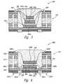
- FIGS. 3-6illustrate device packages having arrangements in accordance with further embodiments of the invention, all of which use some or all of the techniques and arrangements described above with reference to FIGS. 1A-2B .
- FIG. 3illustrates a package 300 having a support member 310 generally similar to the support member 110 shown in FIG. 1E .
- the support member 310carries first, second and third microelectronic devices 340 a , 340 b , and 340 c , each of which may have a different size and/or configuration.
- the first microelectronic device 340 ahas a larger planform footprint than the second microelectronic device 340 b , which in turn has a larger planform footprint than the third microelectronic device 340 c . Because the device bond sites 341 a - 341 c of each microelectronic device 340 a - 340 c are laterally offset from the device bond sites of the microelectronic device immediately above, all three devices 340 a - 340 c can be stacked on each other prior to wire bonding any of the microelectronic devices 340 a - 340 c to corresponding internal bond sites 303 .
- An advantage of this arrangementis that it can reduce the time required to form the package 300 because multiple similar steps can be performed sequentially at one processing station without moving the package 300 back and forth multiple times between processing stations.
- all three microelectronic devices 340 a - 340 ccan be stacked while the package remains at a stacking station, and all three microelectronic devices 340 a - 340 c can be wire bonded while the package 300 remains at a wire bonding station.
- similar, identical, or otherwise related device bond sites 341can be coupled to a corresponding single internal bond site 303 .
- the package 300may include multiple internal bond sites 303 , all at the first conductive layer 322 , and each dedicated to a corresponding device bond site 341 of one of the microelectronic devices 340 a - 340 c . Further details of another arrangement in which individual microelectronic devices may be coupled to corresponding individual bond sites are described below with reference to FIGS. 4 and 5 .
- FIG. 4illustrates a package 400 that includes a support member 410 carrying a first microelectronic device 440 a , and a stacked second microelectronic device 440 b .
- the first microelectronic device 440 acan be coupled to first package bond sites 401 a
- the second microelectronic device 440 bcan be coupled to second package bond sites 401 b that are electrically isolated from the first package bond sites 401 a . Accordingly, electrical signals can be sent to and from the first microelectronic device 440 a independently of signals sent to and from the second microelectronic device 440 b.
- the support member 410can include a first conductive layer 422 and a second conductive layer 433 .
- the first microelectronic device 440 acan be electrically coupled to first internal bond sites 403 a located at the second conductive layer 433 , e.g., with wire bonds 406 or other suitable couplers.
- the second conductive layer 433can be patterned to provide an electrical signal path between the first internal bond sites 403 a and corresponding first package bond sites 401 a , also located at the second conductive layer 433 .
- the second microelectronic device 440 bcan be electrically coupled to second internal bond sites 403 b located at the first conductive layer 422 .
- the first conductive layer 422can be patterned and coupled with appropriate vias 411 to corresponding second package bond sites 401 b located at the second conductive layer 433 .
- the electrical signal path between the first package bond sites 401 a and the first microelectronic device 440 acan be electrically isolated from the electrical signal path between the second package bond sites 401 b and the second microelectronic device 440 b . Accordingly, signals may be transmitted to and from the first microelectronic device 420 a independently of signals transmitted to and from the second microelectronic device 420 b .
- a similar arrangementcan be used to provide independent signal paths to more (e.g., three) microelectronic devices carried by a single support member.
- FIG. 4also illustrates (in dashed lines) another embodiment in which electrical connections to the first microelectronic device 440 a may be made with solder balls 409 .
- the solder balls 409can be positioned between the second conductive layer 433 and bond sites that are accessible from a downwardly facing second surface 443 of the first microelectronic device 440 a , rather than the upwardly facing first surface 442 .
- the second conductive layer 433can both carry the first microelectronic device 440 a and provide electrical signal paths to the first microelectronic device 440 a.
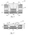
- FIG. 5illustrates a package 500 arranged so that the package bond sites for different dies within the package 500 are accessible from different directions.
- the package 500can include a support member 510 having a first conductive layer 522 and a second conductive layer 533 .
- a first microelectronic device 540 acan be electrically connected with wire bonds to first package bond sites 501 a located at the second conductive layer 533 .
- a second microelectronic device 540 bcan be connected with wire bonds to second package bond sites 501 b located at the first conductive layer 522 . As is shown in FIG. 5 , the first package bond sites 501 a and the second package bond sites 501 b are accessible from opposite sides of the package 500 .
- FIGS. 1A-5illustrate support members formed from multiple elements and configured to carry multiple microelectronic devices.
- the support membermay be formed from a single element, and/or may carry only a single microelectronic device.
- FIG. 6illustrates a package 600 that includes both a single-element support member 610 and a single microelectronic device 640 .
- the support member 610can include a single support member element 620 (e.g., a single circuit board) having a first conductive layer 632 , a second conductive layer 633 , and an insulating layer 621 between the first and second conductive layers 622 , 633 .
- Vias 611can provide for electrical coupling between the two conductive layers 622 , 633 .
- a cavity 616can be formed in the support member 610 using an etching technique or another appropriate technique.
- the microelectronic device 640can be positioned in the cavity 610 so that it is placed against the second conductive layer 633 .
- the microelectronic device 640can then be coupled to corresponding internal bond sites 603 with wire bonds 606 or other appropriate electrical couplings.
- the microelectronic device 640can be shorter than the walls of the cavity 616 , so as not to project above the cavity 616 .
- the microelectronic device 640can project above the cavity 616 , so long as a corresponding encapsulant 604 can still be positioned to protect the wire bonds 606 and the connections between the wire bonds and both the microelectronic device 640 and the support member 610 .
- An advantage of an embodiment of the single-element support member 610 shown in FIG. 6is that it may be simpler and therefore faster and/or less expensive to manufacture than are multi-element support members.
- the single-element support membermay, in at least some embodiments, be thinner than a multi-element support member, and may therefore be particularly appropriate for packages having thin single dies or thin multi-die stacks.
- embodiments of the multi-element support membersmay be particularly appropriate for thicker dies and/or die stacks.
- microelectronic devices and corresponding support memberscan have configurations other than those shown in the Figures.
- electrical couplings other than the wire bondsmay be used to electrically couple the microelectronic devices to bond sites internal to the package, and/or couplings other than solder balls may be used to connect the resulting package to external devices.
- Couplings that include any combination of wire bonds, vias, patterned layers, and/or other featuresmay be used to electrically couple microelectronic devices to externally-accessible package bond sites. Accordingly, the invention not limited except as by the appended claims.
Landscapes
- Engineering & Computer Science (AREA)
- Microelectronics & Electronic Packaging (AREA)
- Power Engineering (AREA)
- Computer Hardware Design (AREA)
- General Physics & Mathematics (AREA)
- Condensed Matter Physics & Semiconductors (AREA)
- Physics & Mathematics (AREA)
- Chemical & Material Sciences (AREA)
- Dispersion Chemistry (AREA)
- Manufacturing & Machinery (AREA)
- Wire Bonding (AREA)
- Packaging Frangible Articles (AREA)
- Die Bonding (AREA)
- Container, Conveyance, Adherence, Positioning, Of Wafer (AREA)
Abstract
Description
Claims (42)
Priority Applications (2)
| Application Number | Priority Date | Filing Date | Title |
|---|---|---|---|
| US13/399,659US8441132B2 (en) | 2006-03-29 | 2012-02-17 | Packaged microelectronic devices recessed in support member cavities, and associated methods |
| US13/893,638US8975745B2 (en) | 2006-03-29 | 2013-05-14 | Packaged microelectronic devices recessed in support member cavities, and associated methods |
Applications Claiming Priority (2)
| Application Number | Priority Date | Filing Date | Title |
|---|---|---|---|
| SG200602089-5 | 2006-03-29 | ||
| SG200602089-5ASG136009A1 (en) | 2006-03-29 | 2006-03-29 | Packaged microelectronic devices recessed in support member cavities, and associated methods |
Related Child Applications (1)
| Application Number | Title | Priority Date | Filing Date |
|---|---|---|---|
| US13/399,659DivisionUS8441132B2 (en) | 2006-03-29 | 2012-02-17 | Packaged microelectronic devices recessed in support member cavities, and associated methods |
Publications (2)
| Publication Number | Publication Date |
|---|---|
| US20070228577A1 US20070228577A1 (en) | 2007-10-04 |
| US8202754B2true US8202754B2 (en) | 2012-06-19 |
Family
ID=38557614
Family Applications (3)
| Application Number | Title | Priority Date | Filing Date |
|---|---|---|---|
| US11/452,750Active2026-09-24US8202754B2 (en) | 2006-03-29 | 2006-06-13 | Packaged microelectronic devices recessed in support member cavities, and associated methods |
| US13/399,659Expired - Fee RelatedUS8441132B2 (en) | 2006-03-29 | 2012-02-17 | Packaged microelectronic devices recessed in support member cavities, and associated methods |
| US13/893,638ActiveUS8975745B2 (en) | 2006-03-29 | 2013-05-14 | Packaged microelectronic devices recessed in support member cavities, and associated methods |
Family Applications After (2)
| Application Number | Title | Priority Date | Filing Date |
|---|---|---|---|
| US13/399,659Expired - Fee RelatedUS8441132B2 (en) | 2006-03-29 | 2012-02-17 | Packaged microelectronic devices recessed in support member cavities, and associated methods |
| US13/893,638ActiveUS8975745B2 (en) | 2006-03-29 | 2013-05-14 | Packaged microelectronic devices recessed in support member cavities, and associated methods |
Country Status (2)
| Country | Link |
|---|---|
| US (3) | US8202754B2 (en) |
| SG (2) | SG136009A1 (en) |
Families Citing this family (3)
| Publication number | Priority date | Publication date | Assignee | Title |
|---|---|---|---|---|
| SG136009A1 (en) | 2006-03-29 | 2007-10-29 | Micron Technology Inc | Packaged microelectronic devices recessed in support member cavities, and associated methods |
| US7851331B2 (en)* | 2006-11-27 | 2010-12-14 | Taiwan Semiconductor Manufacturing Co., Ltd. | Bonding structures and methods of forming bonding structures |
| US8637987B2 (en) | 2011-08-09 | 2014-01-28 | Micron Technology, Inc. | Semiconductor assemblies with multi-level substrates and associated methods of manufacturing |
Citations (94)
| Publication number | Priority date | Publication date | Assignee | Title |
|---|---|---|---|---|
| US5128831A (en) | 1991-10-31 | 1992-07-07 | Micron Technology, Inc. | High-density electronic package comprising stacked sub-modules which are electrically interconnected by solder-filled vias |
| US5252857A (en) | 1991-08-05 | 1993-10-12 | International Business Machines Corporation | Stacked DCA memory chips |
| US5518957A (en) | 1991-10-10 | 1996-05-21 | Samsung Electronics Co., Ltd. | Method for making a thin profile semiconductor package |
| US5593927A (en) | 1993-10-14 | 1997-01-14 | Micron Technology, Inc. | Method for packaging semiconductor dice |
| US5677566A (en) | 1995-05-08 | 1997-10-14 | Micron Technology, Inc. | Semiconductor chip package |
| US5696033A (en) | 1995-08-16 | 1997-12-09 | Micron Technology, Inc. | Method for packaging a semiconductor die |
| US5739585A (en) | 1995-11-27 | 1998-04-14 | Micron Technology, Inc. | Single piece package for semiconductor die |
| USD394844S (en) | 1997-04-25 | 1998-06-02 | Micron Technology, Inc. | Temporary package for semiconductor dice |
| USD402638S (en) | 1997-04-25 | 1998-12-15 | Micron Technology, Inc. | Temporary package for semiconductor dice |
| US5851845A (en) | 1995-12-18 | 1998-12-22 | Micron Technology, Inc. | Process for packaging a semiconductor die using dicing and testing |
| US5883426A (en) | 1996-04-18 | 1999-03-16 | Nec Corporation | Stack module |
| US5891753A (en) | 1997-01-24 | 1999-04-06 | Micron Technology, Inc. | Method and apparatus for packaging flip chip bare die on printed circuit boards |
| US5893726A (en) | 1997-12-15 | 1999-04-13 | Micron Technology, Inc. | Semiconductor package with pre-fabricated cover and method of fabrication |
| US5933713A (en) | 1998-04-06 | 1999-08-03 | Micron Technology, Inc. | Method of forming overmolded chip scale package and resulting product |
| US5938956A (en) | 1996-09-10 | 1999-08-17 | Micron Technology, Inc. | Circuit and method for heating an adhesive to package or rework a semiconductor die |
| US5946553A (en) | 1991-06-04 | 1999-08-31 | Micron Technology, Inc. | Process for manufacturing a semiconductor package with bi-substrate die |
| US5958100A (en) | 1993-06-03 | 1999-09-28 | Micron Technology, Inc. | Process of making a glass semiconductor package |
| US5986209A (en) | 1997-07-09 | 1999-11-16 | Micron Technology, Inc. | Package stack via bottom leaded plastic (BLP) packaging |
| US5989941A (en) | 1997-12-12 | 1999-11-23 | Micron Technology, Inc. | Encapsulated integrated circuit packaging |
| US5990566A (en) | 1998-05-20 | 1999-11-23 | Micron Technology, Inc. | High density semiconductor package |
| US5994784A (en) | 1997-12-18 | 1999-11-30 | Micron Technology, Inc. | Die positioning in integrated circuit packaging |
| USRE36469E (en) | 1988-09-30 | 1999-12-28 | Micron Technology, Inc. | Packaging for semiconductor logic devices |
| US6008070A (en) | 1998-05-21 | 1999-12-28 | Micron Technology, Inc. | Wafer level fabrication and assembly of chip scale packages |
| US6008074A (en) | 1998-10-01 | 1999-12-28 | Micron Technology, Inc. | Method of forming a synchronous-link dynamic random access memory edge-mounted device |
| US6020629A (en) | 1998-06-05 | 2000-02-01 | Micron Technology, Inc. | Stacked semiconductor package and method of fabrication |
| US6025728A (en) | 1997-04-25 | 2000-02-15 | Micron Technology, Inc. | Semiconductor package with wire bond protective member |
| US6028365A (en) | 1998-03-30 | 2000-02-22 | Micron Technology, Inc. | Integrated circuit package and method of fabrication |
| US6046496A (en) | 1997-11-04 | 2000-04-04 | Micron Technology Inc | Chip package |
| US6049125A (en) | 1997-12-29 | 2000-04-11 | Micron Technology, Inc. | Semiconductor package with heat sink and method of fabrication |
| US6048755A (en) | 1998-11-12 | 2000-04-11 | Micron Technology, Inc. | Method for fabricating BGA package using substrate with patterned solder mask open in die attach area |
| US6048744A (en) | 1997-09-15 | 2000-04-11 | Micron Technology, Inc. | Integrated circuit package alignment feature |
| US6051878A (en) | 1997-03-10 | 2000-04-18 | Micron Technology, Inc. | Method of constructing stacked packages |
| US6072233A (en) | 1998-05-04 | 2000-06-06 | Micron Technology, Inc. | Stackable ball grid array package |
| US6072236A (en) | 1996-03-07 | 2000-06-06 | Micron Technology, Inc. | Micromachined chip scale package |
| US6075288A (en) | 1998-06-08 | 2000-06-13 | Micron Technology, Inc. | Semiconductor package having interlocking heat sinks and method of fabrication |
| US6097087A (en) | 1997-10-31 | 2000-08-01 | Micron Technology, Inc. | Semiconductor package including flex circuit, interconnects and dense array external contacts |
| US6103547A (en) | 1997-01-17 | 2000-08-15 | Micron Technology, Inc. | High speed IC package configuration |
| US6107680A (en) | 1995-01-04 | 2000-08-22 | Micron Technology, Inc. | Packaging for bare dice employing EMR-sensitive adhesives |
| US6107122A (en) | 1997-08-04 | 2000-08-22 | Micron Technology, Inc. | Direct die contact (DDC) semiconductor package |
| US6117382A (en) | 1998-02-05 | 2000-09-12 | Micron Technology, Inc. | Method for encasing array packages |
| US6159764A (en) | 1997-07-02 | 2000-12-12 | Micron Technology, Inc. | Varied-thickness heat sink for integrated circuit (IC) packages and method of fabricating IC packages |
| US6172419B1 (en) | 1998-02-24 | 2001-01-09 | Micron Technology, Inc. | Low profile ball grid array package |
| US6175149B1 (en) | 1998-02-13 | 2001-01-16 | Micron Technology, Inc. | Mounting multiple semiconductor dies in a package |
| US6184465B1 (en) | 1998-11-12 | 2001-02-06 | Micron Technology, Inc. | Semiconductor package |
| US6198172B1 (en) | 1997-02-20 | 2001-03-06 | Micron Technology, Inc. | Semiconductor chip package |
| US6208519B1 (en) | 1999-08-31 | 2001-03-27 | Micron Technology, Inc. | Thermally enhanced semiconductor package |
| US6210992B1 (en) | 1999-08-31 | 2001-04-03 | Micron Technology, Inc. | Controlling packaging encapsulant leakage |
| US6215175B1 (en) | 1998-07-06 | 2001-04-10 | Micron Technology, Inc. | Semiconductor package having metal foil die mounting plate |
| US6212767B1 (en) | 1999-08-31 | 2001-04-10 | Micron Technology, Inc. | Assembling a stacked die package |
| US6225689B1 (en) | 1998-08-21 | 2001-05-01 | Micron Technology, Inc. | Low profile multi-IC chip package connector |
| US6229202B1 (en) | 2000-01-10 | 2001-05-08 | Micron Technology, Inc. | Semiconductor package having downset leadframe for reducing package bow |
| US6228548B1 (en) | 1998-02-27 | 2001-05-08 | Micron Technology, Inc. | Method of making a multichip semiconductor package |
| US6235554B1 (en) | 1995-11-27 | 2001-05-22 | Micron Technology, Inc. | Method for fabricating stackable chip scale semiconductor package |
| US6252308B1 (en) | 1996-05-24 | 2001-06-26 | Micron Technology, Inc. | Packaged die PCB with heat sink encapsulant |
| US6259153B1 (en) | 1998-08-20 | 2001-07-10 | Micron Technology, Inc. | Transverse hybrid LOC package |
| US6277671B1 (en) | 1998-10-20 | 2001-08-21 | Micron Technology, Inc. | Methods of forming integrated circuit packages |
| US20010016370A1 (en) | 1999-10-18 | 2001-08-23 | Thin Film Module, Inc. | Low cost decal material used for packaging |
| US6281577B1 (en) | 1996-06-28 | 2001-08-28 | Pac Tech-Packaging Technologies Gmbh | Chips arranged in plurality of planes and electrically connected to one another |
| US6284571B1 (en) | 1997-07-02 | 2001-09-04 | Micron Technology, Inc. | Lead frame assemblies with voltage reference plane and IC packages including same |
| US6291894B1 (en) | 1998-08-31 | 2001-09-18 | Micron Technology, Inc. | Method and apparatus for a semiconductor package for vertical surface mounting |
| US6294839B1 (en) | 1999-08-30 | 2001-09-25 | Micron Technology, Inc. | Apparatus and methods of packaging and testing die |
| US6297547B1 (en) | 1998-02-13 | 2001-10-02 | Micron Technology Inc. | Mounting multiple semiconductor dies in a package |
| US6303981B1 (en) | 1999-09-01 | 2001-10-16 | Micron Technology, Inc. | Semiconductor package having stacked dice and leadframes and method of fabrication |
| US6303985B1 (en) | 1998-11-12 | 2001-10-16 | Micron Technology, Inc. | Semiconductor lead frame and package with stiffened mounting paddle |
| US6310390B1 (en) | 1999-04-08 | 2001-10-30 | Micron Technology, Inc. | BGA package and method of fabrication |
| US6314639B1 (en) | 1998-02-23 | 2001-11-13 | Micron Technology, Inc. | Chip scale package with heat spreader and method of manufacture |
| US6316285B1 (en) | 1998-09-02 | 2001-11-13 | Micron Technology, Inc. | Passivation layer for packaged integrated circuits |
| US6326698B1 (en) | 2000-06-08 | 2001-12-04 | Micron Technology, Inc. | Semiconductor devices having protective layers thereon through which contact pads are exposed and stereolithographic methods of fabricating such semiconductor devices |
| US6326244B1 (en) | 1998-09-03 | 2001-12-04 | Micron Technology, Inc. | Method of making a cavity ball grid array apparatus |
| US6326687B1 (en) | 1998-09-01 | 2001-12-04 | Micron Technology, Inc. | IC package with dual heat spreaders |
| US6329220B1 (en) | 1999-11-23 | 2001-12-11 | Micron Technology, Inc. | Packages for semiconductor die |
| US6331453B1 (en) | 1999-12-16 | 2001-12-18 | Micron Technology, Inc. | Method for fabricating semiconductor packages using mold tooling fixture with flash control cavities |
| US6331221B1 (en) | 1998-04-15 | 2001-12-18 | Micron Technology, Inc. | Process for providing electrical connection between a semiconductor die and a semiconductor die receiving member |
| US6365434B1 (en) | 2000-06-28 | 2002-04-02 | Micron Technology, Inc. | Method and apparatus for reduced flash encapsulation of microelectronic devices |
| US6451709B1 (en) | 1998-09-03 | 2002-09-17 | Micron Technology, Inc. | Methodology of removing misplaced encapsulant for attachment of heat sinks in a chip on board package |
| US6548376B2 (en) | 2001-08-30 | 2003-04-15 | Micron Technology, Inc. | Methods of thinning microelectronic workpieces |
| US6548757B1 (en) | 2000-08-28 | 2003-04-15 | Micron Technology, Inc. | Microelectronic device assemblies having a shielded input and methods for manufacturing and operating such microelectronic device assemblies |
| US6552910B1 (en) | 2000-06-28 | 2003-04-22 | Micron Technology, Inc. | Stacked-die assemblies with a plurality of microelectronic devices and methods of manufacture |
| US6560117B2 (en) | 2000-06-28 | 2003-05-06 | Micron Technology, Inc. | Packaged microelectronic die assemblies and methods of manufacture |
| US6558600B1 (en) | 2000-05-04 | 2003-05-06 | Micron Technology, Inc. | Method for packaging microelectronic substrates |
| US6561479B1 (en) | 2000-08-23 | 2003-05-13 | Micron Technology, Inc. | Small scale actuators and methods for their formation and use |
| US6564979B2 (en) | 2001-07-18 | 2003-05-20 | Micron Technology, Inc. | Method and apparatus for dispensing adhesive on microelectronic substrate supports |
| US6576495B1 (en) | 2000-08-30 | 2003-06-10 | Micron Technology, Inc. | Microelectronic assembly with pre-disposed fill material and associated method of manufacture |
| US6576494B1 (en) | 2000-06-28 | 2003-06-10 | Micron Technology, Inc. | Recessed encapsulated microelectronic devices and methods for formation |
| US6589820B1 (en) | 2000-06-16 | 2003-07-08 | Micron Technology, Inc. | Method and apparatus for packaging a microelectronic die |
| US6607937B1 (en) | 2000-08-23 | 2003-08-19 | Micron Technology, Inc. | Stacked microelectronic dies and methods for stacking microelectronic dies |
| US6614092B2 (en) | 2000-08-16 | 2003-09-02 | Micron Technology, Inc. | Microelectronic device package with conductive elements and associated method of manufacture |
| US6622380B1 (en) | 2002-02-12 | 2003-09-23 | Micron Technology, Inc. | Methods for manufacturing microelectronic devices and methods for mounting microelectronic packages to circuit boards |
| US6670719B2 (en) | 1999-08-25 | 2003-12-30 | Micron Technology, Inc. | Microelectronic device package filled with liquid or pressurized gas and associated method of manufacture |
| US6673649B1 (en) | 2002-07-05 | 2004-01-06 | Micron Technology, Inc. | Microelectronic device packages and methods for controlling the disposition of non-conductive materials in such packages |
| US6746894B2 (en) | 2001-03-30 | 2004-06-08 | Micron Technology, Inc. | Ball grid array interposer, packages and methods |
| US20050224956A1 (en) | 2004-04-02 | 2005-10-13 | Chin-Li Kao | Chip package structure and chip packaging process |
| US20070069371A1 (en)* | 2005-09-29 | 2007-03-29 | United Test And Assembly Center Ltd. | Cavity chip package |
| EP1089336B1 (en) | 1999-09-22 | 2008-02-13 | Lucent Technologies Inc. | Integrated circuit packages with improved EMI characteristics |
Family Cites Families (5)
| Publication number | Priority date | Publication date | Assignee | Title |
|---|---|---|---|---|
| US6379988B1 (en) | 2000-05-16 | 2002-04-30 | Sandia Corporation | Pre-release plastic packaging of MEMS and IMEMS devices |
| US6773962B2 (en) | 2001-03-15 | 2004-08-10 | General Electric Company | Microelectromechanical system device packaging method |
| US7952190B2 (en) | 2003-06-27 | 2011-05-31 | Intel Corporation | Fabrication of microelectronic devices |
| US7145226B2 (en) | 2003-06-30 | 2006-12-05 | Intel Corporation | Scalable microelectronic package using conductive risers |
| SG136009A1 (en) | 2006-03-29 | 2007-10-29 | Micron Technology Inc | Packaged microelectronic devices recessed in support member cavities, and associated methods |
- 2006
- 2006-03-29SGSG200602089-5Apatent/SG136009A1/enunknown
- 2006-03-29SGSG2011048030Apatent/SG172743A1/enunknown
- 2006-06-13USUS11/452,750patent/US8202754B2/enactiveActive
- 2012
- 2012-02-17USUS13/399,659patent/US8441132B2/ennot_activeExpired - Fee Related
- 2013
- 2013-05-14USUS13/893,638patent/US8975745B2/enactiveActive
Patent Citations (109)
| Publication number | Priority date | Publication date | Assignee | Title |
|---|---|---|---|---|
| USRE36469E (en) | 1988-09-30 | 1999-12-28 | Micron Technology, Inc. | Packaging for semiconductor logic devices |
| US5946553A (en) | 1991-06-04 | 1999-08-31 | Micron Technology, Inc. | Process for manufacturing a semiconductor package with bi-substrate die |
| US6020624A (en) | 1991-06-04 | 2000-02-01 | Micron Technology, Inc. | Semiconductor package with bi-substrate die |
| US5252857A (en) | 1991-08-05 | 1993-10-12 | International Business Machines Corporation | Stacked DCA memory chips |
| US5518957A (en) | 1991-10-10 | 1996-05-21 | Samsung Electronics Co., Ltd. | Method for making a thin profile semiconductor package |
| US5128831A (en) | 1991-10-31 | 1992-07-07 | Micron Technology, Inc. | High-density electronic package comprising stacked sub-modules which are electrically interconnected by solder-filled vias |
| US5958100A (en) | 1993-06-03 | 1999-09-28 | Micron Technology, Inc. | Process of making a glass semiconductor package |
| US5593927A (en) | 1993-10-14 | 1997-01-14 | Micron Technology, Inc. | Method for packaging semiconductor dice |
| US6107680A (en) | 1995-01-04 | 2000-08-22 | Micron Technology, Inc. | Packaging for bare dice employing EMR-sensitive adhesives |
| US5677566A (en) | 1995-05-08 | 1997-10-14 | Micron Technology, Inc. | Semiconductor chip package |
| US5696033A (en) | 1995-08-16 | 1997-12-09 | Micron Technology, Inc. | Method for packaging a semiconductor die |
| US5739585A (en) | 1995-11-27 | 1998-04-14 | Micron Technology, Inc. | Single piece package for semiconductor die |
| US6235554B1 (en) | 1995-11-27 | 2001-05-22 | Micron Technology, Inc. | Method for fabricating stackable chip scale semiconductor package |
| US5851845A (en) | 1995-12-18 | 1998-12-22 | Micron Technology, Inc. | Process for packaging a semiconductor die using dicing and testing |
| US6124634A (en) | 1996-03-07 | 2000-09-26 | Micron Technology, Inc. | Micromachined chip scale package |
| US6072236A (en) | 1996-03-07 | 2000-06-06 | Micron Technology, Inc. | Micromachined chip scale package |
| US5883426A (en) | 1996-04-18 | 1999-03-16 | Nec Corporation | Stack module |
| US6252308B1 (en) | 1996-05-24 | 2001-06-26 | Micron Technology, Inc. | Packaged die PCB with heat sink encapsulant |
| US6281577B1 (en) | 1996-06-28 | 2001-08-28 | Pac Tech-Packaging Technologies Gmbh | Chips arranged in plurality of planes and electrically connected to one another |
| US5938956A (en) | 1996-09-10 | 1999-08-17 | Micron Technology, Inc. | Circuit and method for heating an adhesive to package or rework a semiconductor die |
| US6103547A (en) | 1997-01-17 | 2000-08-15 | Micron Technology, Inc. | High speed IC package configuration |
| US5898224A (en) | 1997-01-24 | 1999-04-27 | Micron Technology, Inc. | Apparatus for packaging flip chip bare die on printed circuit boards |
| US5891753A (en) | 1997-01-24 | 1999-04-06 | Micron Technology, Inc. | Method and apparatus for packaging flip chip bare die on printed circuit boards |
| US6198172B1 (en) | 1997-02-20 | 2001-03-06 | Micron Technology, Inc. | Semiconductor chip package |
| US6051878A (en) | 1997-03-10 | 2000-04-18 | Micron Technology, Inc. | Method of constructing stacked packages |
| US6025728A (en) | 1997-04-25 | 2000-02-15 | Micron Technology, Inc. | Semiconductor package with wire bond protective member |
| USD394844S (en) | 1997-04-25 | 1998-06-02 | Micron Technology, Inc. | Temporary package for semiconductor dice |
| USD402638S (en) | 1997-04-25 | 1998-12-15 | Micron Technology, Inc. | Temporary package for semiconductor dice |
| US6284571B1 (en) | 1997-07-02 | 2001-09-04 | Micron Technology, Inc. | Lead frame assemblies with voltage reference plane and IC packages including same |
| US6159764A (en) | 1997-07-02 | 2000-12-12 | Micron Technology, Inc. | Varied-thickness heat sink for integrated circuit (IC) packages and method of fabricating IC packages |
| US5986209A (en) | 1997-07-09 | 1999-11-16 | Micron Technology, Inc. | Package stack via bottom leaded plastic (BLP) packaging |
| US6150717A (en) | 1997-08-04 | 2000-11-21 | Micron Technology, Inc. | Direct die contact (DDC) semiconductor package |
| US6107122A (en) | 1997-08-04 | 2000-08-22 | Micron Technology, Inc. | Direct die contact (DDC) semiconductor package |
| US6048744A (en) | 1997-09-15 | 2000-04-11 | Micron Technology, Inc. | Integrated circuit package alignment feature |
| US6246108B1 (en) | 1997-09-15 | 2001-06-12 | Micron Technology, Inc. | Integrated circuit package including lead frame with electrically isolated alignment feature |
| US6097087A (en) | 1997-10-31 | 2000-08-01 | Micron Technology, Inc. | Semiconductor package including flex circuit, interconnects and dense array external contacts |
| US6046496A (en) | 1997-11-04 | 2000-04-04 | Micron Technology Inc | Chip package |
| US5989941A (en) | 1997-12-12 | 1999-11-23 | Micron Technology, Inc. | Encapsulated integrated circuit packaging |
| US5893726A (en) | 1997-12-15 | 1999-04-13 | Micron Technology, Inc. | Semiconductor package with pre-fabricated cover and method of fabrication |
| US5994784A (en) | 1997-12-18 | 1999-11-30 | Micron Technology, Inc. | Die positioning in integrated circuit packaging |
| US6326242B1 (en) | 1997-12-29 | 2001-12-04 | Micron Technology, Inc. | Semiconductor package with heat sink and method of fabrication |
| US6049125A (en) | 1997-12-29 | 2000-04-11 | Micron Technology, Inc. | Semiconductor package with heat sink and method of fabrication |
| US6332766B1 (en) | 1998-02-05 | 2001-12-25 | Micron Technology, Inc. | Apparatus for encasing array packages |
| US6117382A (en) | 1998-02-05 | 2000-09-12 | Micron Technology, Inc. | Method for encasing array packages |
| US6175149B1 (en) | 1998-02-13 | 2001-01-16 | Micron Technology, Inc. | Mounting multiple semiconductor dies in a package |
| US6297547B1 (en) | 1998-02-13 | 2001-10-02 | Micron Technology Inc. | Mounting multiple semiconductor dies in a package |
| US6314639B1 (en) | 1998-02-23 | 2001-11-13 | Micron Technology, Inc. | Chip scale package with heat spreader and method of manufacture |
| US6172419B1 (en) | 1998-02-24 | 2001-01-09 | Micron Technology, Inc. | Low profile ball grid array package |
| US6429528B1 (en) | 1998-02-27 | 2002-08-06 | Micron Technology, Inc. | Multichip semiconductor package |
| US6228548B1 (en) | 1998-02-27 | 2001-05-08 | Micron Technology, Inc. | Method of making a multichip semiconductor package |
| US6028365A (en) | 1998-03-30 | 2000-02-22 | Micron Technology, Inc. | Integrated circuit package and method of fabrication |
| US5933713A (en) | 1998-04-06 | 1999-08-03 | Micron Technology, Inc. | Method of forming overmolded chip scale package and resulting product |
| US6331221B1 (en) | 1998-04-15 | 2001-12-18 | Micron Technology, Inc. | Process for providing electrical connection between a semiconductor die and a semiconductor die receiving member |
| US6072233A (en) | 1998-05-04 | 2000-06-06 | Micron Technology, Inc. | Stackable ball grid array package |
| US5990566A (en) | 1998-05-20 | 1999-11-23 | Micron Technology, Inc. | High density semiconductor package |
| US6008070A (en) | 1998-05-21 | 1999-12-28 | Micron Technology, Inc. | Wafer level fabrication and assembly of chip scale packages |
| US6326697B1 (en) | 1998-05-21 | 2001-12-04 | Micron Technology, Inc. | Hermetically sealed chip scale packages formed by wafer level fabrication and assembly |
| US6020629A (en) | 1998-06-05 | 2000-02-01 | Micron Technology, Inc. | Stacked semiconductor package and method of fabrication |
| US6075288A (en) | 1998-06-08 | 2000-06-13 | Micron Technology, Inc. | Semiconductor package having interlocking heat sinks and method of fabrication |
| US6215175B1 (en) | 1998-07-06 | 2001-04-10 | Micron Technology, Inc. | Semiconductor package having metal foil die mounting plate |
| US6259153B1 (en) | 1998-08-20 | 2001-07-10 | Micron Technology, Inc. | Transverse hybrid LOC package |
| US6258623B1 (en) | 1998-08-21 | 2001-07-10 | Micron Technology, Inc. | Low profile multi-IC chip package connector |
| US6225689B1 (en) | 1998-08-21 | 2001-05-01 | Micron Technology, Inc. | Low profile multi-IC chip package connector |
| US6291894B1 (en) | 1998-08-31 | 2001-09-18 | Micron Technology, Inc. | Method and apparatus for a semiconductor package for vertical surface mounting |
| US6326687B1 (en) | 1998-09-01 | 2001-12-04 | Micron Technology, Inc. | IC package with dual heat spreaders |
| US6316285B1 (en) | 1998-09-02 | 2001-11-13 | Micron Technology, Inc. | Passivation layer for packaged integrated circuits |
| US6326244B1 (en) | 1998-09-03 | 2001-12-04 | Micron Technology, Inc. | Method of making a cavity ball grid array apparatus |
| US6451709B1 (en) | 1998-09-03 | 2002-09-17 | Micron Technology, Inc. | Methodology of removing misplaced encapsulant for attachment of heat sinks in a chip on board package |
| US6008074A (en) | 1998-10-01 | 1999-12-28 | Micron Technology, Inc. | Method of forming a synchronous-link dynamic random access memory edge-mounted device |
| US6277671B1 (en) | 1998-10-20 | 2001-08-21 | Micron Technology, Inc. | Methods of forming integrated circuit packages |
| US6184465B1 (en) | 1998-11-12 | 2001-02-06 | Micron Technology, Inc. | Semiconductor package |
| US6048755A (en) | 1998-11-12 | 2000-04-11 | Micron Technology, Inc. | Method for fabricating BGA package using substrate with patterned solder mask open in die attach area |
| US6303985B1 (en) | 1998-11-12 | 2001-10-16 | Micron Technology, Inc. | Semiconductor lead frame and package with stiffened mounting paddle |
| US6310390B1 (en) | 1999-04-08 | 2001-10-30 | Micron Technology, Inc. | BGA package and method of fabrication |
| US6670719B2 (en) | 1999-08-25 | 2003-12-30 | Micron Technology, Inc. | Microelectronic device package filled with liquid or pressurized gas and associated method of manufacture |
| US6294839B1 (en) | 1999-08-30 | 2001-09-25 | Micron Technology, Inc. | Apparatus and methods of packaging and testing die |
| US6210992B1 (en) | 1999-08-31 | 2001-04-03 | Micron Technology, Inc. | Controlling packaging encapsulant leakage |
| US6212767B1 (en) | 1999-08-31 | 2001-04-10 | Micron Technology, Inc. | Assembling a stacked die package |
| US6208519B1 (en) | 1999-08-31 | 2001-03-27 | Micron Technology, Inc. | Thermally enhanced semiconductor package |
| US6303981B1 (en) | 1999-09-01 | 2001-10-16 | Micron Technology, Inc. | Semiconductor package having stacked dice and leadframes and method of fabrication |
| EP1089336B1 (en) | 1999-09-22 | 2008-02-13 | Lucent Technologies Inc. | Integrated circuit packages with improved EMI characteristics |
| US20010016370A1 (en) | 1999-10-18 | 2001-08-23 | Thin Film Module, Inc. | Low cost decal material used for packaging |
| US6329220B1 (en) | 1999-11-23 | 2001-12-11 | Micron Technology, Inc. | Packages for semiconductor die |
| US6331453B1 (en) | 1999-12-16 | 2001-12-18 | Micron Technology, Inc. | Method for fabricating semiconductor packages using mold tooling fixture with flash control cavities |
| US6229202B1 (en) | 2000-01-10 | 2001-05-08 | Micron Technology, Inc. | Semiconductor package having downset leadframe for reducing package bow |
| US6258624B1 (en) | 2000-01-10 | 2001-07-10 | Micron Technology, Inc. | Semiconductor package having downset leadframe for reducing package bow |
| US6558600B1 (en) | 2000-05-04 | 2003-05-06 | Micron Technology, Inc. | Method for packaging microelectronic substrates |
| US6326698B1 (en) | 2000-06-08 | 2001-12-04 | Micron Technology, Inc. | Semiconductor devices having protective layers thereon through which contact pads are exposed and stereolithographic methods of fabricating such semiconductor devices |
| US6653173B2 (en) | 2000-06-16 | 2003-11-25 | Micron Technology, Inc. | Method and apparatus for packaging a microelectronic die |
| US6589820B1 (en) | 2000-06-16 | 2003-07-08 | Micron Technology, Inc. | Method and apparatus for packaging a microelectronic die |
| US6560117B2 (en) | 2000-06-28 | 2003-05-06 | Micron Technology, Inc. | Packaged microelectronic die assemblies and methods of manufacture |
| US6638595B2 (en) | 2000-06-28 | 2003-10-28 | Micron Technology, Inc. | Method and apparatus for reduced flash encapsulation of microelectronic devices |
| US6365434B1 (en) | 2000-06-28 | 2002-04-02 | Micron Technology, Inc. | Method and apparatus for reduced flash encapsulation of microelectronic devices |
| US6644949B2 (en) | 2000-06-28 | 2003-11-11 | Micron Technology, Inc. | Apparatus for reduced flash encapsulation of microelectronic devices |
| US6576494B1 (en) | 2000-06-28 | 2003-06-10 | Micron Technology, Inc. | Recessed encapsulated microelectronic devices and methods for formation |
| US6552910B1 (en) | 2000-06-28 | 2003-04-22 | Micron Technology, Inc. | Stacked-die assemblies with a plurality of microelectronic devices and methods of manufacture |
| US6614092B2 (en) | 2000-08-16 | 2003-09-02 | Micron Technology, Inc. | Microelectronic device package with conductive elements and associated method of manufacture |
| US6672325B2 (en) | 2000-08-23 | 2004-01-06 | Micron Technology, Inc. | Small scale actuators and methods for their formation and use |
| US6607937B1 (en) | 2000-08-23 | 2003-08-19 | Micron Technology, Inc. | Stacked microelectronic dies and methods for stacking microelectronic dies |
| US6561479B1 (en) | 2000-08-23 | 2003-05-13 | Micron Technology, Inc. | Small scale actuators and methods for their formation and use |
| US6548757B1 (en) | 2000-08-28 | 2003-04-15 | Micron Technology, Inc. | Microelectronic device assemblies having a shielded input and methods for manufacturing and operating such microelectronic device assemblies |
| US6576495B1 (en) | 2000-08-30 | 2003-06-10 | Micron Technology, Inc. | Microelectronic assembly with pre-disposed fill material and associated method of manufacture |
| US6746894B2 (en) | 2001-03-30 | 2004-06-08 | Micron Technology, Inc. | Ball grid array interposer, packages and methods |
| US6564979B2 (en) | 2001-07-18 | 2003-05-20 | Micron Technology, Inc. | Method and apparatus for dispensing adhesive on microelectronic substrate supports |
| US6548376B2 (en) | 2001-08-30 | 2003-04-15 | Micron Technology, Inc. | Methods of thinning microelectronic workpieces |
| US6622380B1 (en) | 2002-02-12 | 2003-09-23 | Micron Technology, Inc. | Methods for manufacturing microelectronic devices and methods for mounting microelectronic packages to circuit boards |
| US6673649B1 (en) | 2002-07-05 | 2004-01-06 | Micron Technology, Inc. | Microelectronic device packages and methods for controlling the disposition of non-conductive materials in such packages |
| US20050224956A1 (en) | 2004-04-02 | 2005-10-13 | Chin-Li Kao | Chip package structure and chip packaging process |
| US20070069371A1 (en)* | 2005-09-29 | 2007-03-29 | United Test And Assembly Center Ltd. | Cavity chip package |
Non-Patent Citations (1)
| Title |
|---|
| Search Report and Written Opinion for Singapore Application No. 200602089-5, Sep. 29, 2008. |
Also Published As
| Publication number | Publication date |
|---|---|
| US8975745B2 (en) | 2015-03-10 |
| US8441132B2 (en) | 2013-05-14 |
| US20130249092A1 (en) | 2013-09-26 |
| SG172743A1 (en) | 2011-07-28 |
| US20070228577A1 (en) | 2007-10-04 |
| SG136009A1 (en) | 2007-10-29 |
| US20120146239A1 (en) | 2012-06-14 |
Similar Documents
| Publication | Publication Date | Title |
|---|---|---|
| US7692931B2 (en) | Microelectronic packages with leadframes, including leadframes configured for stacked die packages, and associated systems and methods | |
| US6621156B2 (en) | Semiconductor device having stacked multi chip module structure | |
| US7326592B2 (en) | Stacked die package | |
| US6906415B2 (en) | Semiconductor device assemblies and packages including multiple semiconductor devices and methods | |
| US8349649B2 (en) | Semiconductor device and manufacturing method thereof | |
| JP3892259B2 (en) | Manufacturing method of semiconductor device | |
| JP6027966B2 (en) | Stackable mold microelectronic package with area array unit connector | |
| US10651050B2 (en) | Semiconductor device packages and structures | |
| JP2009508324A (en) | Microelectronic device, stacked microelectronic device, and method of manufacturing microelectronic device | |
| JP2009508324A6 (en) | Microelectronic device, stacked microelectronic device, and method of manufacturing microelectronic device | |
| US20100140801A1 (en) | Device | |
| US9917073B2 (en) | Reconstituted wafer-level package dram with conductive interconnects formed in encapsulant at periphery of the package | |
| KR19990006158A (en) | Ball grid array package | |
| WO2014088071A1 (en) | Semiconductor device | |
| US9271403B2 (en) | Semiconductor assemblies with multi-level substrates and associated methods of manufacturing | |
| KR20130077939A (en) | Semiconductor package having one-layer substrate and, fan-out semiconductor package and method for manufacturing the same | |
| JPWO2003012863A1 (en) | Semiconductor device and manufacturing method thereof | |
| US8975745B2 (en) | Packaged microelectronic devices recessed in support member cavities, and associated methods | |
| JP2000299432A (en) | Manufacture of semiconductor device | |
| US8410598B2 (en) | Semiconductor package and method of manufacturing the same | |
| KR101123797B1 (en) | Semiconductor package and stacked semiconductor package having the same | |
| JP2008294318A (en) | Semiconductor device, and manufacturing method thereof | |
| JP2008182285A (en) | Semiconductor device and manufacturing method thereof |
Legal Events
| Date | Code | Title | Description |
|---|---|---|---|
| AS | Assignment | Owner name:MICRON TECHNOLOGY, INC., IDAHO Free format text:ASSIGNMENT OF ASSIGNORS INTEREST;ASSIGNORS:CORISIS, DAVID J.;CHONG, CHIN HUI;LEE, CHOON KUAN;REEL/FRAME:017976/0987;SIGNING DATES FROM 20060518 TO 20060522 Owner name:MICRON TECHNOLOGY, INC., IDAHO Free format text:ASSIGNMENT OF ASSIGNORS INTEREST;ASSIGNORS:CORISIS, DAVID J.;CHONG, CHIN HUI;LEE, CHOON KUAN;SIGNING DATES FROM 20060518 TO 20060522;REEL/FRAME:017976/0987 | |
| FEPP | Fee payment procedure | Free format text:PAYOR NUMBER ASSIGNED (ORIGINAL EVENT CODE: ASPN); ENTITY STATUS OF PATENT OWNER: LARGE ENTITY | |
| STCF | Information on status: patent grant | Free format text:PATENTED CASE | |
| CC | Certificate of correction | ||
| FPAY | Fee payment | Year of fee payment:4 | |
| AS | Assignment | Owner name:U.S. BANK NATIONAL ASSOCIATION, AS COLLATERAL AGENT, CALIFORNIA Free format text:SECURITY INTEREST;ASSIGNOR:MICRON TECHNOLOGY, INC.;REEL/FRAME:038669/0001 Effective date:20160426 Owner name:U.S. BANK NATIONAL ASSOCIATION, AS COLLATERAL AGEN Free format text:SECURITY INTEREST;ASSIGNOR:MICRON TECHNOLOGY, INC.;REEL/FRAME:038669/0001 Effective date:20160426 | |
| AS | Assignment | Owner name:MORGAN STANLEY SENIOR FUNDING, INC., AS COLLATERAL AGENT, MARYLAND Free format text:PATENT SECURITY AGREEMENT;ASSIGNOR:MICRON TECHNOLOGY, INC.;REEL/FRAME:038954/0001 Effective date:20160426 Owner name:MORGAN STANLEY SENIOR FUNDING, INC., AS COLLATERAL Free format text:PATENT SECURITY AGREEMENT;ASSIGNOR:MICRON TECHNOLOGY, INC.;REEL/FRAME:038954/0001 Effective date:20160426 | |
| AS | Assignment | Owner name:U.S. BANK NATIONAL ASSOCIATION, AS COLLATERAL AGENT, CALIFORNIA Free format text:CORRECTIVE ASSIGNMENT TO CORRECT THE REPLACE ERRONEOUSLY FILED PATENT #7358718 WITH THE CORRECT PATENT #7358178 PREVIOUSLY RECORDED ON REEL 038669 FRAME 0001. ASSIGNOR(S) HEREBY CONFIRMS THE SECURITY INTEREST;ASSIGNOR:MICRON TECHNOLOGY, INC.;REEL/FRAME:043079/0001 Effective date:20160426 Owner name:U.S. BANK NATIONAL ASSOCIATION, AS COLLATERAL AGEN Free format text:CORRECTIVE ASSIGNMENT TO CORRECT THE REPLACE ERRONEOUSLY FILED PATENT #7358718 WITH THE CORRECT PATENT #7358178 PREVIOUSLY RECORDED ON REEL 038669 FRAME 0001. ASSIGNOR(S) HEREBY CONFIRMS THE SECURITY INTEREST;ASSIGNOR:MICRON TECHNOLOGY, INC.;REEL/FRAME:043079/0001 Effective date:20160426 | |
| AS | Assignment | Owner name:JPMORGAN CHASE BANK, N.A., AS COLLATERAL AGENT, ILLINOIS Free format text:SECURITY INTEREST;ASSIGNORS:MICRON TECHNOLOGY, INC.;MICRON SEMICONDUCTOR PRODUCTS, INC.;REEL/FRAME:047540/0001 Effective date:20180703 Owner name:JPMORGAN CHASE BANK, N.A., AS COLLATERAL AGENT, IL Free format text:SECURITY INTEREST;ASSIGNORS:MICRON TECHNOLOGY, INC.;MICRON SEMICONDUCTOR PRODUCTS, INC.;REEL/FRAME:047540/0001 Effective date:20180703 | |
| AS | Assignment | Owner name:MICRON TECHNOLOGY, INC., IDAHO Free format text:RELEASE BY SECURED PARTY;ASSIGNOR:U.S. BANK NATIONAL ASSOCIATION, AS COLLATERAL AGENT;REEL/FRAME:047243/0001 Effective date:20180629 | |
| AS | Assignment | Owner name:MICRON TECHNOLOGY, INC., IDAHO Free format text:RELEASE BY SECURED PARTY;ASSIGNOR:MORGAN STANLEY SENIOR FUNDING, INC., AS COLLATERAL AGENT;REEL/FRAME:050937/0001 Effective date:20190731 | |
| AS | Assignment | Owner name:MICRON SEMICONDUCTOR PRODUCTS, INC., IDAHO Free format text:RELEASE BY SECURED PARTY;ASSIGNOR:JPMORGAN CHASE BANK, N.A., AS COLLATERAL AGENT;REEL/FRAME:051028/0001 Effective date:20190731 Owner name:MICRON TECHNOLOGY, INC., IDAHO Free format text:RELEASE BY SECURED PARTY;ASSIGNOR:JPMORGAN CHASE BANK, N.A., AS COLLATERAL AGENT;REEL/FRAME:051028/0001 Effective date:20190731 | |
| MAFP | Maintenance fee payment | Free format text:PAYMENT OF MAINTENANCE FEE, 8TH YEAR, LARGE ENTITY (ORIGINAL EVENT CODE: M1552); ENTITY STATUS OF PATENT OWNER: LARGE ENTITY Year of fee payment:8 | |
| MAFP | Maintenance fee payment | Free format text:PAYMENT OF MAINTENANCE FEE, 12TH YEAR, LARGE ENTITY (ORIGINAL EVENT CODE: M1553); ENTITY STATUS OF PATENT OWNER: LARGE ENTITY Year of fee payment:12 |