US8199556B2 - Methods of reading and using memory cells - Google Patents
Methods of reading and using memory cellsDownload PDFInfo
- Publication number
- US8199556B2 US8199556B2US12/564,265US56426509AUS8199556B2US 8199556 B2US8199556 B2US 8199556B2US 56426509 AUS56426509 AUS 56426509AUS 8199556 B2US8199556 B2US 8199556B2
- Authority
- US
- United States
- Prior art keywords
- memory cell
- voltage
- reading
- memory
- memristor
- Prior art date
- Legal status (The legal status is an assumption and is not a legal conclusion. Google has not performed a legal analysis and makes no representation as to the accuracy of the status listed.)
- Active, expires
Links
Images


Classifications
- G—PHYSICS
- G11—INFORMATION STORAGE
- G11C—STATIC STORES
- G11C13/00—Digital stores characterised by the use of storage elements not covered by groups G11C11/00, G11C23/00, or G11C25/00
- G11C13/0002—Digital stores characterised by the use of storage elements not covered by groups G11C11/00, G11C23/00, or G11C25/00 using resistive RAM [RRAM] elements
- G11C13/0021—Auxiliary circuits
- G11C13/004—Reading or sensing circuits or methods
- G—PHYSICS
- G11—INFORMATION STORAGE
- G11C—STATIC STORES
- G11C16/00—Erasable programmable read-only memories
- G11C16/02—Erasable programmable read-only memories electrically programmable
- G11C16/06—Auxiliary circuits, e.g. for writing into memory
- G11C16/26—Sensing or reading circuits; Data output circuits
- G—PHYSICS
- G11—INFORMATION STORAGE
- G11C—STATIC STORES
- G11C13/00—Digital stores characterised by the use of storage elements not covered by groups G11C11/00, G11C23/00, or G11C25/00
- G11C13/0002—Digital stores characterised by the use of storage elements not covered by groups G11C11/00, G11C23/00, or G11C25/00 using resistive RAM [RRAM] elements
- G11C13/0007—Digital stores characterised by the use of storage elements not covered by groups G11C11/00, G11C23/00, or G11C25/00 using resistive RAM [RRAM] elements comprising metal oxide memory material, e.g. perovskites
- G—PHYSICS
- G11—INFORMATION STORAGE
- G11C—STATIC STORES
- G11C13/00—Digital stores characterised by the use of storage elements not covered by groups G11C11/00, G11C23/00, or G11C25/00
- G11C13/0002—Digital stores characterised by the use of storage elements not covered by groups G11C11/00, G11C23/00, or G11C25/00 using resistive RAM [RRAM] elements
- G11C13/0021—Auxiliary circuits
- G11C13/0061—Timing circuits or methods
- G—PHYSICS
- G11—INFORMATION STORAGE
- G11C—STATIC STORES
- G11C16/00—Erasable programmable read-only memories
- G11C16/02—Erasable programmable read-only memories electrically programmable
- G11C16/06—Auxiliary circuits, e.g. for writing into memory
- G11C16/10—Programming or data input circuits
- G—PHYSICS
- G11—INFORMATION STORAGE
- G11C—STATIC STORES
- G11C13/00—Digital stores characterised by the use of storage elements not covered by groups G11C11/00, G11C23/00, or G11C25/00
- G11C13/0002—Digital stores characterised by the use of storage elements not covered by groups G11C11/00, G11C23/00, or G11C25/00 using resistive RAM [RRAM] elements
- G11C13/0021—Auxiliary circuits
- G11C13/004—Reading or sensing circuits or methods
- G11C2013/0052—Read process characterized by the shape, e.g. form, length, amplitude of the read pulse
- G—PHYSICS
- G11—INFORMATION STORAGE
- G11C—STATIC STORES
- G11C2213/00—Indexing scheme relating to G11C13/00 for features not covered by this group
- G11C2213/70—Resistive array aspects
- G11C2213/72—Array wherein the access device being a diode
Definitions
- Memory cellsare common constituents of integrated circuitry.
- An individual memory cellcomprises a device that exists in two or more stable memory states.
- the act of “writing” to the devicecomprises placing the device into a desired memory state; and the act of “reading” the device comprises determination of which of the memory states the device is in.
- the writing to the devicemay comprise imparting a programming voltage to the device, with the programming voltage being a voltage sufficient to cause the device to change from one memory state to another.
- the reading of the devicemay comprise measurement of an electrical parameter influenced by the memory state of the device, such as, for example, measurement of current passing through the device. It can be desired that the reading be conducted under conditions which do not alter the memory state of the device, so that the reading operation does not “write” to the device.
- One way of avoiding undesired alteration of the memory state of a memory device during a reading operationis to conduct the reading at a voltage much less than the programming voltage.
- differences between the memory states of memory devicesmay become larger, and thus more easily measured, as voltages on the devices are increased.
- the reading of a memory devicemay comprise a trade-off between a desire to read the device accurately and quickly, and a desire to avoid alteration of the memory state of the device during the reading operation.
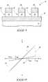
- FIG. 1is a diagrammatic cross-sectional view of a region of a semiconductor construction, illustrating a portion of a memory array.
- FIG. 2is a graphical illustration of current vs. voltage relationships of an example memory cell.
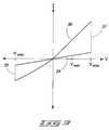
- FIG. 3is a graphical illustration of current vs. voltage relationships of another example memory cell.
- FIG. 4is a graphical illustration of voltage vs. time relationships of an example memory cell, and illustrates a lag occurring during a writing operation.
- FIG. 5is a graphical illustration of voltage vs. time relationships of the example memory cell of FIG. 4 , and illustrates a read operation being conducted with a duration much shorter than the lag of the writing operation.
- FIG. 6is a graphical illustration of current vs. voltage relationships of an example memory cell, and illustrates current differences between memory states that will coincide with read operations conducted at various voltages.
- FIG. 7is a diagrammatic cross-sectional view of a region of a semiconductor construction, illustrating a portion of another example memory array.
- FIG. 8is a graphical illustration of current vs. voltage relationships of an example non-ohmic device.
- the programming of memory cellsmay comprise provision of sufficient voltage (often called a programming voltage) to the cells to enable the cells to transition from one memory state to another.
- a programming voltagesufficient voltage
- Some memory cellshave a significant lag (three microseconds or more) between the time that a programming voltage is applied and the time that the cells transition from one memory state to another. Such lag may be the result of atomic and/or molecular rearrangements occurring in the memory cells during the transitioning between the memory states.
- the memory cells that experience significant lag in transitioning from one memory state to anotherare sometimes referred to as being “frequency dependent” relative to a writing operation.
- the term “frequency dependent”is utilized to indicate that a programming pulse will need to be provided for a specific duration before the memory cell will switch from one memory state to another. For instance, if a memory cell has a lag of three microseconds (3 ⁇ 10 ⁇ 6 seconds), then a programming pulse will need to be provided for at least three microseconds during a write operation in order to switch the memory cell from one memory state to another. Another way to express this is that the programming pulse will need to have a frequency of less than or equal to the inverse of 3 ⁇ 10 ⁇ 6 seconds (i.e., less than or equal to 3.3 ⁇ 10 5 sec ⁇ 1 ).
- Memory cells containing non-ohmic componentsoften have frequency dependent writing operations.
- the frequency dependency of the writing operationsmay be considered problematic in the prior art, in that such slows down the writing operations.
- some embodiments of the present inventiontake advantage of the frequency dependency of the writing operations to enhance the reading operations of the memory devices.
- FIG. 1A portion of an example array of memory cells is shown in FIG. 1 as part of a semiconductor construction 10 .
- the constructionincludes a substrate 12 supporting a plurality of memory cells 14 , 16 and 18 .
- the memory cellscomprise memory cell structures 20 .
- the memory cell structuresare shown to be homogeneous, such structures may be nonhomogeneous in some embodiments; and may, for example, comprise a stack of two or more compositionally-different layers.
- the memory cell structuresmay comprise any suitable composition or combination of compositions configured to have at least two stable memory states which may be interchanged by exposing the memory cell structures to a changed condition (for instance, by applying a voltage across the memory cell).
- the memory cellsmay comprise configurations having frequency dependent writing operations, and in some embodiments may comprise non-ohmic devices; such as, for example, memristors and/or diodes.
- the memory cell structuresmay comprise titanium oxide.
- the titanium oxidemay be provided in two separate phases within the memory cell structures, with one of the phases being relatively oxygen rich and the other being relatively oxygen deficient.
- the titanium oxidemay be provided between a pair of platinum electrodes.
- the memristorsmay comprise one or both of crystalline zirconium oxide and crystalline hafnium oxide between a pair of titanium nitride electrodes. If the memory cell structures include memristors that comprise oxide between a pair of electrodes, such oxide may be referred to as memory cell material.
- the construction 10includes a plurality of electrically conductive lines 22 , 24 , 26 and 28 .
- the lines 24 , 26 and 28extend orthogonally to the line 22 , and extend in and out of the page relative to the cross-section of FIG. 1 .
- the lines 22 , 24 , 26 and 28may comprise any suitable electrically conductive composition, or combination of compositions; and in some embodiments may comprise one or more of various metals (for instance, platinum, titanium, tungsten, etc.), metal-containing compounds (for instance, metal silicides, metal nitride, etc.), and conductively-doped semiconductor materials (for instance, silicon, germanium, etc.).
- the linesare shown to be homogeneous, the lines may be nonhomogeneous in some embodiments; and may, for example, comprise stacks of two or more compositionally-different layers.
- the electrodes discussed above regarding example memristorsmay be comprised by the lines adjacent the memory structure, or may be comprised by the memory structure itself.
- Each of the memory cells 14 , 16 and 18is at an intersection where two orthogonal lines cross.
- the crossing linesmay be utilized to uniquely address the various memory cells.
- memory cell 14may be uniquely addressed as the cell triggered when electrical input is provided along both of lines 22 and 24 .
- the writing to cell 14will comprise provision of a programming voltage across the cell.
- the programming voltagewill correspond to a voltage differential between line 24 and line 22 .
- Such voltage differentialmay be delivered to the cell by providing part of the differential along line 22 and the other part across line 24 .
- a write voltage of “q” millivoltsis to be provided to cell 14 (where “q” is any appropriate number)
- a fraction of the “q” millivoltsmay be provided along line 22 (for instance q/2) and a remaining fraction of the “q” millivolts may be provided along line 24 (for instance, ⁇ q/2) so that a total voltage differential across memory cell 14 is “q” millivolts.
- the cellmay be referred to as a half-select memory device. It can be advantageous to utilize half-select devices, in that this can reduce the voltage carried by any line, and can thus reduce undesired effects on neighboring cells when addressing a specific cell.
- the reading of information from a memory cellmay also comprise application of a voltage differential across the cell, and such differential may be carried across the intersecting lines analogously to the situation discussed above regarding the writing of information to the memory cells.
- Substrate 12may comprise any suitable composition or combination of compositions.
- substrate 12may be a semiconductor substrate, and may comprise, consist essentially of, or consist of, for example, monocrystalline silicon lightly-doped with background p-type dopant.
- semiconductor substrateand “semiconductor substrate” mean any construction comprising semiconductive material, including, but not limited to, bulk semiconductive materials such as a semiconductive wafer (either alone or in assemblies comprising other materials thereon), and semiconductive material layers (either alone or in assemblies comprising other materials).
- substratemeans any supporting structure, including, but not limited to, the semiconductive substrates described above.
- the substratemay be nonhomogeneous in some embodiments; and may, for example, comprise various structures and layers associated with integrated circuit fabrication. Such structures and layers may comprise any suitable electrical properties of the constructions being fabricated, and may thus be electrically conductive, electrically insulative, or semiconductive, in various embodiments.
- FIG. 2shows a graph of current (I) versus voltage (V), and illustrates operation of an example memory cell.
- the graphmay be considered to comprise two intersecting lines 30 and 32 that cross at the origin. Each line corresponds to a different memory state of the memory cell.
- the signs of the current and voltageare such that the difference between lines 30 and 32 is negative on the left half of the graph and positive on the right half of the graph.
- absolute valuethe term “absolute value” having the classical mathematical meaning of being the numerical value of a number regardless of sign.
- the memory states corresponding to lines 30 and 32cannot be distinguished from one another. However, as the absolute value of the voltage increases, the states become discernible from one another. Specifically, the absolute value of current through the memory cell at any given voltage is higher when the cell is in the memory state 30 than when the cell is in the memory state 32 . The absolute value of the current difference between the memory states 30 and 32 increases as the absolute value of the voltage increases until the absolute value of the voltage reaches a level corresponding to the write voltage (V write or ⁇ V write ). At the write voltage, the memory states 30 and 32 interchange with one another (as represented by the dashed lines 31 and 33 ).
- the performance of the memory cellis symmetric about the origin.
- the absolute value of current flowing through the memory cellis identical regardless of whether positive voltage is applied or negative voltage is applied.
- the only difference between the current flow induced by negative voltage relative to that induced by positive voltageis the direction of the current flow; which is illustrated in the graph as a difference between whether the current flow is positive or negative.
- Reading of the memory cell represented by the graph of FIG. 2corresponds to a determination of whether the memory cell is in the memory state represented by line 32 , or the memory state represented by line 30 .
- Such determinationmay comprise applying a voltage to the memory cell, and then determining if the current flow through the memory cell is high enough to correspond to state 30 , or instead corresponds to state 32 .
- the difference between states 30 and 32is larger, and accordingly easier to detect, at voltages having a high absolute value than at voltages having a low absolute value. Accordingly, the state of the memory cell may be read with higher accuracy at voltages having a high absolute value than at voltages having a low absolute value.
- V read or ⁇ V readthe voltage utilized during the read operation
- V read or ⁇ V readthe state of the cell may be disturbed during the read operation to the extent that the cell may switch from one state to another—which would destroy the accuracy of the read operation.
- conventional methods of reading memory cellsutilize an absolute value of V read that is sufficiently below the absolute value of V write to avoid inadvertently altering the state of the memory cell during the read operation.
- V read voltagesare illustrated in FIG. 2 as having absolute values well below the absolute values of the V write voltages.
- Some embodiments of the invention(discussed below with reference to FIGS. 3-8 ) take advantage of the lag times of frequency dependent write operations to enable the absolute voltage of a read operation to approach, or even exceed, the absolute voltage of a write operation.
- FIG. 2shows a memory cell having symmetric performance regardless of whether positive voltage is applied to the memory cell or negative voltage is applied.
- the embodiments described hereinmay be utilized with either memory cells having symmetric performance relative to positive and negative voltage, or with memory cells having asymmetric performance relative to positive and negative voltage.
- FIG. 3shows a graph of current (I) versus voltage (V) for operation of an example memory cell that has asymmetric performance relative to positive voltage and negative voltage.
- the graph of FIG. 3comprises two intersecting lines 34 and 36 that cross at the origin. Each line corresponds to a different memory state of the memory cell. At zero voltage (i.e., at the origin of the graph of FIG. 3 ), the memory states cannot be distinguished from one another.
- the absolute value of the voltageincreases, the absolute value of current through the memory cell is higher when the cell is in the memory state 36 relative to when the cell is in the memory state 34 .
- the absolute value of the current difference between the memory states 34 and 36increases regardless of whether positive voltage is applied to the memory cell, or negative voltage is applied. However, the current difference between the two states changes more quickly when positive voltage is applied than when negative voltage is applied. Thus, it is easier to read the cell using positive voltage during the read operation than it is using negative voltage.
- the example read voltage (V read )is shown as a positive voltage.
- the asymmetric memory cell represented in FIG. 3has a greater difference occurring between states 34 and 36 at positive voltage than negative voltage, other asymmetric cells may have the greater difference occurring at negative voltage than at positive voltage.
- the asymmetric memory cell of FIG. 3is similar to the symmetric cell of FIG. 2 in that once the absolute value of the voltage reaches a level corresponding to the write voltage (V write or ⁇ V write ), the memory states 34 and 36 can interchange with one another, (as represented by the dashed lines 35 and 37 ).
- FIG. 4graphically illustrates a relationship of voltage versus time for a memory cell that has a lag during a write operation.
- the voltage applied to the deviceis at an initial value V 1 , which is less than the programming voltage.
- V 1the voltage is increased to a second value V 2 which corresponds to the programming voltage.
- the programming voltageis maintained for a period of time; and the writing operation does not occur at the time T 1 , but rather at a time T 2 subsequent to T 1 .
- the delay between the time T 1 when the programming voltage is initially applied, and the time T 2 when the writing operation is complete,is a lag in the response of the memory cell to the programming voltage.
- Such lagmay be due to, for example, time needed for atomic and/or molecular rearrangement in the memory cell in transitioning from one memory state to another.
- the duration of the programming pulse from T 1 to T 2will vary depending on various factors which may include, for example, the type of material utilized in the memory cell, the programming voltage, and the amount of material utilized in the memory cell.
- the memory cellwill not change from one memory state to another unless a pulse of sufficient voltage is provided for a sufficient duration of time. Since a time duration may be converted to a frequency by simply taking the inverse of the time duration, the memory cell having the programming characteristics shown in FIG. 4 may be alternatively described as having a frequency dependent write operation.
- the voltages V 1 and V 2 of FIG. 4may be absolute values of voltages as graphed, and the actual voltages utilized during the writing operation may be either negative voltages or positive voltages.
- FIG. 5graphically illustrates a relationship of voltage versus time for the memory cell of FIG. 4 during a reading operation, with such reading operation being superimposed on the writing operation described above with reference to FIG. 4 (the writing operation is shown in dashed-line in FIG. 5 ).
- the reading operationutilizes a voltage V R , and in the embodiment of FIG. 5 such voltage is greater than the programming voltage V 2 utilized during the writing operation.
- the reading voltage V Rmay be equal to the programming voltage, or less than the programming voltage.
- the reading voltage V Ris initiated at the time T 1 and maintained until the time T R .
- the duration between the times T R and T 1is much less than the duration required for the writing operation (i.e., the duration between the times T 2 and T 1 ).
- the duration utilized for the reading operationmay be at least about an order of magnitude shorter (i.e., at least about 10 times shorter) than the duration necessary for the writing operation.
- the short voltage pulse utilized for the read operationcan enable the read operation to be conducted at high voltage without inadvertently causing a write operation. Specifically, the voltage pulse utilized for the read operation is conducted for too short of a duration to overcome the lag of the writing operation, and therefore the memory cell does not change from one memory state to another in spite of the high voltage utilized during the read operation.
- a memory cellmay comprise a memristor containing titanium oxide and having a write operation requiring a duration of at least about three microseconds to complete the transition from one memory state to another.
- the read operationmay be conducted with a pulse having a duration of less than or equal to about 0.3 microseconds (or other words, having a frequency of at least about 3.3 ⁇ 10 6 seconds ⁇ 1 ).
- the memory cellmay comprise a memristor having a write operation requiring a duration of at least about one millisecond to complete the transition from one memory state to another, and the read operation may be conducted with a pulse having a duration of less than or equal to 0.1 milliseconds.
- the reading of a non-ohmic devicemay meet performance specifications of a bipolar memristor type RRAM device (i.e., current density “J” of about 1 ⁇ 10 4 A/cm 2 at ⁇ 2.8V, and of about 100 A/cm 2 at ⁇ 2.0V).
- non-ohmic select devicesmay be connected in electrical series with memristors of memory cells (for instance, memory cell structure 20 of FIG. 1 may be comprised by memristors, and diodes may be connected in electrical series with the memristors of the memory cells 14 , 16 and 18 as select devices for the individual memory cells), and the duration of the reading operation may be tailored for the electrical series combinations of the memristors and the non-ohmic select devices.
- FIG. 7shows a construction 60 which is similar to the construction 10 of FIG.
- non-ohmic select devices 62 , 64 and 66for instance, diodes
- structures 20may comprise one or more oxides between a pair of platinum electrodes
- the non-ohmic devicesmay comprise one or more insulative materials between a pair of electrodes.
- One of the electrodes of the memristorsmay be shared between the memristor and the adjacent non-ohmic device.
- non-ohmic select devicesmay be provided between lines 24 , 26 and 28 and the memory cell structures alternatively, or in addition to, the provision of the select devices between line 22 and the memory cell structures.
- the select devicesare shown as separate devices from line 22 , in some embodiments the select devices may share conductive material with the line.
- the select devicesmay be diodes containing insulative material between a pair of electrodes, and one of the electrodes may comprise conductive material that is common to line 22 .
- the relative length of the read operation pulse to the minimum duration time required for a write operation of a memory cellmay vary depending on the relative voltages utilized for the read and write operations, and depending on the configuration of the memory cell.
- the example embodimentsdescribe read operation pulses which are an order of magnitude less than the minimum duration required for write operations, in other embodiments it may be possible to utilize read operation pulses which are closer to the minimum durations required for the write operations without risk of having the read operations inadvertently disturb an initial state of the memory cell.
- FIG. 6shows a graph of current (I) versus voltage (V) for the memory cell of FIG. 2 , and illustrates reading operations that may be conducted using reading pulses shorter than a minimum duration required for a write operation.
- the memory cellcomprises the memory states corresponding to the two intersecting lines 30 and 32 . As discussed above regarding FIG. 2 , the memory states become easier to distinguish from one another as the absolute value of the voltage passing through the memory cell increases.
- the voltage levels ⁇ V write and V writecorrespond to the write voltages where the memory states 30 and 32 can interchange with one another.
- FIG. 6illustrates numerous example read voltages (V read1 , V read2 , V read3 , ⁇ V read1 , ⁇ V read2 and ⁇ V read3 ) that may be utilized during reading of the memory cell for determination of whether the memory cell is in the state represented by line 32 , or the state represented by line 30 .
- An advantage of utilizing a read pulse that is shorter than the minimum duration pulse required for a write operation of a frequency dependent memory deviceis that the read operation may be conducted at a voltage greater than or equal to the voltage of the write operation. As shown in FIG. 6 , the difference between states 30 and 32 is larger, and accordingly easier to detect, at higher voltages.
- An advantage of some embodimentsis that the reading of the memory cell may be conducted with a voltage having an absolute value that is at least as large as an absolute value of the voltage utilized during a writing operation, which may enable the state of the memory cell to be read with higher accuracy, and possibly greater speed, than is possible at the lower voltages used for prior art reading operations.
- the current vs. voltage curves of FIGS. 2 , 3 and 6are example curves of some example devices.
- the various embodiments described hereinmay be used with numerous different devices, characterized by different current vs. voltage curves than those shown.
- FIG. 8shows a curve 70 of current vs. voltage for a non-ohmic device that may be utilized additionally, or alternatively, to the devices described by the curves of FIGS. 2 , 3 and 6 .
- the curve 70 of FIG. 8corresponds to one memory state of the device, and persons of ordinary skill will recognize that there may be another curve which corresponds to a different memory state of the device.
- the various embodiments discussed hereinmay have application to any electronic system utilizing memory devices; with example electronic systems including computers, cars, airplanes, clocks, cellular phones, etc.
Landscapes
- Chemical & Material Sciences (AREA)
- Engineering & Computer Science (AREA)
- Materials Engineering (AREA)
- Semiconductor Memories (AREA)
- Read Only Memory (AREA)
Abstract
Description
Claims (26)
Priority Applications (7)
| Application Number | Priority Date | Filing Date | Title |
|---|---|---|---|
| US12/564,265US8199556B2 (en) | 2009-09-22 | 2009-09-22 | Methods of reading and using memory cells |
| KR20127007270AKR101277014B1 (en) | 2009-09-22 | 2010-08-18 | Methods of reading and using memory cells |
| PCT/US2010/045856WO2011037703A2 (en) | 2009-09-22 | 2010-08-18 | Methods of reading and using memory cells |
| CN201080041969.3ACN102498521B (en) | 2009-09-22 | 2010-08-18 | Methods of reading and using memory cells |
| TW099130229ATWI484500B (en) | 2009-09-22 | 2010-09-07 | Methods of reading and using memory cells |
| US13/463,794US8675392B2 (en) | 2009-09-22 | 2012-05-03 | Methods of reading and using memory cells |
| US14/175,030US9135995B2 (en) | 2009-09-22 | 2014-02-07 | Methods of reading and using memristor memory cells with a short read pulse |
Applications Claiming Priority (1)
| Application Number | Priority Date | Filing Date | Title |
|---|---|---|---|
| US12/564,265US8199556B2 (en) | 2009-09-22 | 2009-09-22 | Methods of reading and using memory cells |
Related Child Applications (1)
| Application Number | Title | Priority Date | Filing Date |
|---|---|---|---|
| US13/463,794ContinuationUS8675392B2 (en) | 2009-09-22 | 2012-05-03 | Methods of reading and using memory cells |
Publications (2)
| Publication Number | Publication Date |
|---|---|
| US20110069529A1 US20110069529A1 (en) | 2011-03-24 |
| US8199556B2true US8199556B2 (en) | 2012-06-12 |
Family
ID=43756493
Family Applications (3)
| Application Number | Title | Priority Date | Filing Date |
|---|---|---|---|
| US12/564,265Active2030-06-21US8199556B2 (en) | 2009-09-22 | 2009-09-22 | Methods of reading and using memory cells |
| US13/463,794ActiveUS8675392B2 (en) | 2009-09-22 | 2012-05-03 | Methods of reading and using memory cells |
| US14/175,030Active2029-09-25US9135995B2 (en) | 2009-09-22 | 2014-02-07 | Methods of reading and using memristor memory cells with a short read pulse |
Family Applications After (2)
| Application Number | Title | Priority Date | Filing Date |
|---|---|---|---|
| US13/463,794ActiveUS8675392B2 (en) | 2009-09-22 | 2012-05-03 | Methods of reading and using memory cells |
| US14/175,030Active2029-09-25US9135995B2 (en) | 2009-09-22 | 2014-02-07 | Methods of reading and using memristor memory cells with a short read pulse |
Country Status (5)
| Country | Link |
|---|---|
| US (3) | US8199556B2 (en) |
| KR (1) | KR101277014B1 (en) |
| CN (1) | CN102498521B (en) |
| TW (1) | TWI484500B (en) |
| WO (1) | WO2011037703A2 (en) |
Cited By (7)
| Publication number | Priority date | Publication date | Assignee | Title |
|---|---|---|---|---|
| US20110266515A1 (en)* | 2010-04-28 | 2011-11-03 | Pickett Matthew D | Memristive switch device |
| US20120218810A1 (en)* | 2009-09-22 | 2012-08-30 | Micron Technology, Inc. | Methods Of Reading And Using Memory Cells |
| US20130001498A1 (en)* | 2010-08-12 | 2013-01-03 | Micron Technology, Inc. | Memory Cells, Non-Volatile Memory Arrays, Methods Of Operating Memory Cells, Methods Of Reading To And Writing From A Memory Cell, And Methods Of Programming A Memory Cell |
| US8867261B2 (en) | 2010-02-15 | 2014-10-21 | Micron Technology, Inc. | Memcapacitor devices, field effect transistor devices, and, non-volatile memory arrays |
| US8902639B2 (en) | 2010-02-15 | 2014-12-02 | Micron Technology, Inc. | Cross-point memory cells, non-volatile memory arrays, methods of reading a memory cell, methods of programming a memory cell, methods of writing to and reading from a memory cell, and computer systems |
| US9490011B2 (en) | 2013-07-10 | 2016-11-08 | Hewlett Packard Enterprise Development Lp | Storage device write pulse control |
| US20190122730A1 (en)* | 2016-04-07 | 2019-04-25 | Helmholtz-Zentrum Dresden - Rossendorf E.V. | Method and Means for Operating a Complementary Analogue Reconfigurable Memristive Resistive Switch and Use Thereof as an Artificial Synapse |
Families Citing this family (12)
| Publication number | Priority date | Publication date | Assignee | Title |
|---|---|---|---|---|
| US8848337B2 (en)* | 2011-02-01 | 2014-09-30 | John R. Koza | Signal processing devices having one or more memristors |
| WO2013015803A1 (en) | 2011-07-27 | 2013-01-31 | Hewlett-Packard Development Company, L.P. | Method and system for reducing write-buffer capacities within memristor-based data-storage devices |
| US9349445B2 (en) | 2011-09-16 | 2016-05-24 | Micron Technology, Inc. | Select devices for memory cell applications |
| US9142767B2 (en) | 2011-09-16 | 2015-09-22 | Micron Technology, Inc. | Resistive memory cell including integrated select device and storage element |
| US8780607B2 (en) | 2011-09-16 | 2014-07-15 | Micron Technology, Inc. | Select devices for memory cell applications |
| US8581224B2 (en) | 2012-01-20 | 2013-11-12 | Micron Technology, Inc. | Memory cells |
| US9036395B2 (en) | 2012-06-26 | 2015-05-19 | Hewlett-Packard Development Company, L.P. | Programmed-state detection in memristor stacks |
| US8908415B2 (en)* | 2013-03-01 | 2014-12-09 | Taiwan Semiconductor Manufacturing Company, Ltd. | Resistive memory reset |
| WO2015065415A1 (en)* | 2013-10-31 | 2015-05-07 | Hewlett-Packard Development Company, L.P. | Memristive device switching by alternating polarity pulses |
| DE102013020517B4 (en)* | 2013-12-11 | 2015-06-25 | Forschungszentrum Jülich GmbH | Method for reading out a resistive memory cell and a memory cell for carrying out |
| US9911500B2 (en) | 2016-04-18 | 2018-03-06 | Sandisk Technologies Llc | Dummy voltage to reduce first read effect in memory |
| US10347315B2 (en) | 2017-10-31 | 2019-07-09 | Sandisk Technologies Llc | Group read refresh |
Citations (15)
| Publication number | Priority date | Publication date | Assignee | Title |
|---|---|---|---|---|
| US6842357B2 (en)* | 2002-04-23 | 2005-01-11 | Intel Corporation | Nondestructive sensing mechanism for polarized materials |
| US20060157679A1 (en) | 2005-01-19 | 2006-07-20 | Matrix Semiconductor, Inc. | Structure and method for biasing phase change memory array for reliable writing |
| US20070002665A1 (en)* | 2005-06-29 | 2007-01-04 | Hitesh Windlass | Minimization of signal loss due to self-erase of imprinted data |
| US7236389B2 (en) | 2005-11-17 | 2007-06-26 | Sharp Laboratories Of America, Inc. | Cross-point RRAM memory array having low bit line crosstalk |
| US20070224770A1 (en) | 2006-03-25 | 2007-09-27 | Makoto Nagashima | Systems and methods for fabricating self-aligned memory cell |
| US20070268737A1 (en)* | 2006-05-18 | 2007-11-22 | Renesas Technology Corp. | Nonvolatile memory device |
| US20080043519A1 (en)* | 2006-08-21 | 2008-02-21 | Kabushiki Kaisha Toshiba | Magnetic memory element, magnetic memory having said magnetic memory element, and method for driving magnetic memory |
| US20080165566A1 (en) | 2007-01-04 | 2008-07-10 | Samsung Electronics Co., Ltd. | Non-volatile memory including sub cell array and method of writing data thereto |
| US20080247219A1 (en)* | 2007-04-04 | 2008-10-09 | Samsung Electronics Co., Ltd. | Resistive Random Access Memory Devices Including Sidewall Resistive Layers and Related Methods |
| US7446010B2 (en) | 2005-07-18 | 2008-11-04 | Sharp Laboratories Of America, Inc. | Metal/semiconductor/metal (MSM) back-to-back Schottky diode |
| US20080298143A1 (en)* | 2007-05-31 | 2008-12-04 | Zhiqin Chen | Memory device with delay tracking for improved timing margin |
| US20080308783A1 (en) | 2007-06-14 | 2008-12-18 | Seung-Eon Ahn | Memory devices and methods of manufacturing the same |
| US7471556B2 (en) | 2007-05-15 | 2008-12-30 | Super Talent Electronics, Inc. | Local bank write buffers for accelerating a phase-change memory |
| US20090201715A1 (en)* | 2008-02-11 | 2009-08-13 | Franz Kreupl | Carbon Diode Array for Resistivity Changing Memories |
| WO2011037703A2 (en) | 2009-09-22 | 2011-03-31 | Micron Technology, Inc. | Methods of reading and using memory cells |
Family Cites Families (6)
| Publication number | Priority date | Publication date | Assignee | Title |
|---|---|---|---|---|
| US7095644B2 (en)* | 2003-12-22 | 2006-08-22 | Unity Semiconductor Corporation | Conductive memory array having page mode and burst mode read capability |
| JP4890016B2 (en)* | 2005-03-16 | 2012-03-07 | ルネサスエレクトロニクス株式会社 | Nonvolatile semiconductor memory device |
| US20070279975A1 (en)* | 2006-06-06 | 2007-12-06 | Hudgens Stephen J | Refreshing a phase change memory |
| US7719352B2 (en)* | 2007-03-13 | 2010-05-18 | Qualcomm Incorporated | Active circuits with isolation switches |
| US7499336B2 (en)* | 2007-05-14 | 2009-03-03 | Skymedi Corporation | Method of programming a nonvolatile memory cell and related memory array |
| US7663900B2 (en)* | 2007-12-31 | 2010-02-16 | Hitachi Global Storage Technologies Netherlands B.V. | Tree-structure memory device |
- 2009
- 2009-09-22USUS12/564,265patent/US8199556B2/enactiveActive
- 2010
- 2010-08-18WOPCT/US2010/045856patent/WO2011037703A2/enactiveApplication Filing
- 2010-08-18CNCN201080041969.3Apatent/CN102498521B/enactiveActive
- 2010-08-18KRKR20127007270Apatent/KR101277014B1/enactiveActive
- 2010-09-07TWTW099130229Apatent/TWI484500B/enactive
- 2012
- 2012-05-03USUS13/463,794patent/US8675392B2/enactiveActive
- 2014
- 2014-02-07USUS14/175,030patent/US9135995B2/enactiveActive
Patent Citations (15)
| Publication number | Priority date | Publication date | Assignee | Title |
|---|---|---|---|---|
| US6842357B2 (en)* | 2002-04-23 | 2005-01-11 | Intel Corporation | Nondestructive sensing mechanism for polarized materials |
| US20060157679A1 (en) | 2005-01-19 | 2006-07-20 | Matrix Semiconductor, Inc. | Structure and method for biasing phase change memory array for reliable writing |
| US20070002665A1 (en)* | 2005-06-29 | 2007-01-04 | Hitesh Windlass | Minimization of signal loss due to self-erase of imprinted data |
| US7446010B2 (en) | 2005-07-18 | 2008-11-04 | Sharp Laboratories Of America, Inc. | Metal/semiconductor/metal (MSM) back-to-back Schottky diode |
| US7236389B2 (en) | 2005-11-17 | 2007-06-26 | Sharp Laboratories Of America, Inc. | Cross-point RRAM memory array having low bit line crosstalk |
| US20070224770A1 (en) | 2006-03-25 | 2007-09-27 | Makoto Nagashima | Systems and methods for fabricating self-aligned memory cell |
| US20070268737A1 (en)* | 2006-05-18 | 2007-11-22 | Renesas Technology Corp. | Nonvolatile memory device |
| US20080043519A1 (en)* | 2006-08-21 | 2008-02-21 | Kabushiki Kaisha Toshiba | Magnetic memory element, magnetic memory having said magnetic memory element, and method for driving magnetic memory |
| US20080165566A1 (en) | 2007-01-04 | 2008-07-10 | Samsung Electronics Co., Ltd. | Non-volatile memory including sub cell array and method of writing data thereto |
| US20080247219A1 (en)* | 2007-04-04 | 2008-10-09 | Samsung Electronics Co., Ltd. | Resistive Random Access Memory Devices Including Sidewall Resistive Layers and Related Methods |
| US7471556B2 (en) | 2007-05-15 | 2008-12-30 | Super Talent Electronics, Inc. | Local bank write buffers for accelerating a phase-change memory |
| US20080298143A1 (en)* | 2007-05-31 | 2008-12-04 | Zhiqin Chen | Memory device with delay tracking for improved timing margin |
| US20080308783A1 (en) | 2007-06-14 | 2008-12-18 | Seung-Eon Ahn | Memory devices and methods of manufacturing the same |
| US20090201715A1 (en)* | 2008-02-11 | 2009-08-13 | Franz Kreupl | Carbon Diode Array for Resistivity Changing Memories |
| WO2011037703A2 (en) | 2009-09-22 | 2011-03-31 | Micron Technology, Inc. | Methods of reading and using memory cells |
Non-Patent Citations (3)
| Title |
|---|
| Driscoll et al., "Phase-transition driven memristive system", Applied Physics Letters (Online), vol. 95(4), Jul. 2009. |
| Hummer et al., "Origin of Nanoscale Phase Stability Reversals in Titanium Oxide Polymorphs", The Journal of Physical Chemistry C, vol. 113(11), Feb. 2009, pp. 4240-4245. Abstract Only. |
| Lee, Myoung-Jae, et al., "2-stack 1D-1R Cross-point Structure with Oxide Diodes as Switch Elements for High Density Resistance RAM Applications" IEEE, 2007, pp. 771-774. |
Cited By (20)
| Publication number | Priority date | Publication date | Assignee | Title |
|---|---|---|---|---|
| US8675392B2 (en)* | 2009-09-22 | 2014-03-18 | Micron Technology, Inc. | Methods of reading and using memory cells |
| US20120218810A1 (en)* | 2009-09-22 | 2012-08-30 | Micron Technology, Inc. | Methods Of Reading And Using Memory Cells |
| US9135995B2 (en)* | 2009-09-22 | 2015-09-15 | Micron Technology, Inc. | Methods of reading and using memristor memory cells with a short read pulse |
| US20140153316A1 (en)* | 2009-09-22 | 2014-06-05 | Micron Technology, Inc. | Methods of Reading and Using Memory Cells |
| US9830970B2 (en) | 2010-02-15 | 2017-11-28 | Micron Technology, Inc. | Cross-point memory cells, non-volatile memory arrays, methods of reading a memory cell, methods of programming a memory cell, methods of writing to and reading from a memory cell, and computer systems |
| US9236473B2 (en) | 2010-02-15 | 2016-01-12 | Micron Technology, Inc. | Field effect transistor devices |
| US10796744B2 (en) | 2010-02-15 | 2020-10-06 | Micron Technology, Inc. | Cross-point memory cells, non-volatile memory arrays, methods of reading a memory cell, methods of programming a memory cell, methods of writing to and reading from a memory cell, and computer systems |
| US10360967B2 (en) | 2010-02-15 | 2019-07-23 | Micron Technology, Inc. | Cross-point memory cells, non-volatile memory arrays, methods of reading a memory cell, methods of programming a memory cell, methods of writing to and reading from a memory cell, and computer systems |
| US8867261B2 (en) | 2010-02-15 | 2014-10-21 | Micron Technology, Inc. | Memcapacitor devices, field effect transistor devices, and, non-volatile memory arrays |
| US8902639B2 (en) | 2010-02-15 | 2014-12-02 | Micron Technology, Inc. | Cross-point memory cells, non-volatile memory arrays, methods of reading a memory cell, methods of programming a memory cell, methods of writing to and reading from a memory cell, and computer systems |
| US9419215B2 (en) | 2010-02-15 | 2016-08-16 | Micron Technology, Inc. | Cross-point memory cells, non-volatile memory arrays, methods of reading a memory cell, methods of programming a memory cell, methods of writing to and reading from a memory cell, and computer systems |
| US20110266515A1 (en)* | 2010-04-28 | 2011-11-03 | Pickett Matthew D | Memristive switch device |
| US8586959B2 (en)* | 2010-04-28 | 2013-11-19 | Hewlett-Packard Development Company, L.P. | Memristive switch device |
| US8634224B2 (en) | 2010-08-12 | 2014-01-21 | Micron Technology, Inc. | Memory cells, non-volatile memory arrays, methods of operating memory cells, methods of writing to and reading from a memory cell, and methods of programming a memory cell |
| US9275728B2 (en) | 2010-08-12 | 2016-03-01 | Micron Technology, Inc. | Memory cells, non-volatile memory arrays, methods of operating memory cells, methods of writing to and writing from a memory cell, and methods of programming a memory cell |
| US20130001498A1 (en)* | 2010-08-12 | 2013-01-03 | Micron Technology, Inc. | Memory Cells, Non-Volatile Memory Arrays, Methods Of Operating Memory Cells, Methods Of Reading To And Writing From A Memory Cell, And Methods Of Programming A Memory Cell |
| US8537599B2 (en)* | 2010-08-12 | 2013-09-17 | Micron Technology, Inc. | Memory cells, non-volatile memory arrays, methods of operating memory cells, methods of reading to and writing from a memory cell, and methods of programming a memory cell |
| US9490011B2 (en) | 2013-07-10 | 2016-11-08 | Hewlett Packard Enterprise Development Lp | Storage device write pulse control |
| US20190122730A1 (en)* | 2016-04-07 | 2019-04-25 | Helmholtz-Zentrum Dresden - Rossendorf E.V. | Method and Means for Operating a Complementary Analogue Reconfigurable Memristive Resistive Switch and Use Thereof as an Artificial Synapse |
| US10388370B2 (en)* | 2016-04-07 | 2019-08-20 | Helmholtz-Zentrum Dresden—Rossendorf E.V. | Method and means for operating a complementary analogue reconfigurable memristive resistive switch and use thereof as an artificial synapse |
Also Published As
| Publication number | Publication date |
|---|---|
| WO2011037703A3 (en) | 2011-06-09 |
| US20120218810A1 (en) | 2012-08-30 |
| KR101277014B1 (en) | 2013-06-24 |
| CN102498521A (en) | 2012-06-13 |
| KR20120054080A (en) | 2012-05-29 |
| WO2011037703A2 (en) | 2011-03-31 |
| US8675392B2 (en) | 2014-03-18 |
| TWI484500B (en) | 2015-05-11 |
| TW201133506A (en) | 2011-10-01 |
| US20110069529A1 (en) | 2011-03-24 |
| CN102498521B (en) | 2015-07-22 |
| US9135995B2 (en) | 2015-09-15 |
| US20140153316A1 (en) | 2014-06-05 |
Similar Documents
| Publication | Publication Date | Title |
|---|---|---|
| US8199556B2 (en) | Methods of reading and using memory cells | |
| US10614883B2 (en) | Resistance memory cell | |
| US11398256B2 (en) | Local bit lines and methods of selecting the same to access memory elements in cross-point arrays | |
| US10510411B2 (en) | RRAM array with current limiting element | |
| KR102109600B1 (en) | Semiconductor memory device and driving method thereof | |
| JP4684297B2 (en) | Writing method for nonvolatile semiconductor memory device | |
| JP4880101B1 (en) | Nonvolatile memory device and driving method thereof | |
| US20110188289A1 (en) | Access signal adjustment circuits and methods for memory cells in a cross-point array | |
| US20120075907A1 (en) | Resistor structure for a non-volatile memory device and method | |
| JP6329349B2 (en) | Nonvolatile resistance change memory device and bias method of resistance change memory structure | |
| WO2015053009A1 (en) | Semiconductor device | |
| WO2012169198A1 (en) | Nonvolatile storage element, method of manufacturing thereof, initial breaking method, and nonvolatile storage device | |
| US20120057390A1 (en) | Memory array with write feedback |
Legal Events
| Date | Code | Title | Description |
|---|---|---|---|
| AS | Assignment | Owner name:MICRON TECHNOLOGY, INC., IDAHO Free format text:ASSIGNMENT OF ASSIGNORS INTEREST;ASSIGNORS:SRINIVASAN, BHASKAR;SANCHU, GURTEJ S.;SIGNING DATES FROM 20090910 TO 20090918;REEL/FRAME:023265/0122 | |
| FEPP | Fee payment procedure | Free format text:PAYOR NUMBER ASSIGNED (ORIGINAL EVENT CODE: ASPN); ENTITY STATUS OF PATENT OWNER: LARGE ENTITY | |
| STCF | Information on status: patent grant | Free format text:PATENTED CASE | |
| FPAY | Fee payment | Year of fee payment:4 | |
| AS | Assignment | Owner name:U.S. BANK NATIONAL ASSOCIATION, AS COLLATERAL AGENT, CALIFORNIA Free format text:SECURITY INTEREST;ASSIGNOR:MICRON TECHNOLOGY, INC.;REEL/FRAME:038669/0001 Effective date:20160426 Owner name:U.S. BANK NATIONAL ASSOCIATION, AS COLLATERAL AGEN Free format text:SECURITY INTEREST;ASSIGNOR:MICRON TECHNOLOGY, INC.;REEL/FRAME:038669/0001 Effective date:20160426 | |
| AS | Assignment | Owner name:MORGAN STANLEY SENIOR FUNDING, INC., AS COLLATERAL AGENT, MARYLAND Free format text:PATENT SECURITY AGREEMENT;ASSIGNOR:MICRON TECHNOLOGY, INC.;REEL/FRAME:038954/0001 Effective date:20160426 Owner name:MORGAN STANLEY SENIOR FUNDING, INC., AS COLLATERAL Free format text:PATENT SECURITY AGREEMENT;ASSIGNOR:MICRON TECHNOLOGY, INC.;REEL/FRAME:038954/0001 Effective date:20160426 | |
| AS | Assignment | Owner name:U.S. BANK NATIONAL ASSOCIATION, AS COLLATERAL AGENT, CALIFORNIA Free format text:CORRECTIVE ASSIGNMENT TO CORRECT THE REPLACE ERRONEOUSLY FILED PATENT #7358718 WITH THE CORRECT PATENT #7358178 PREVIOUSLY RECORDED ON REEL 038669 FRAME 0001. ASSIGNOR(S) HEREBY CONFIRMS THE SECURITY INTEREST;ASSIGNOR:MICRON TECHNOLOGY, INC.;REEL/FRAME:043079/0001 Effective date:20160426 Owner name:U.S. BANK NATIONAL ASSOCIATION, AS COLLATERAL AGEN Free format text:CORRECTIVE ASSIGNMENT TO CORRECT THE REPLACE ERRONEOUSLY FILED PATENT #7358718 WITH THE CORRECT PATENT #7358178 PREVIOUSLY RECORDED ON REEL 038669 FRAME 0001. ASSIGNOR(S) HEREBY CONFIRMS THE SECURITY INTEREST;ASSIGNOR:MICRON TECHNOLOGY, INC.;REEL/FRAME:043079/0001 Effective date:20160426 | |
| AS | Assignment | Owner name:JPMORGAN CHASE BANK, N.A., AS COLLATERAL AGENT, ILLINOIS Free format text:SECURITY INTEREST;ASSIGNORS:MICRON TECHNOLOGY, INC.;MICRON SEMICONDUCTOR PRODUCTS, INC.;REEL/FRAME:047540/0001 Effective date:20180703 Owner name:JPMORGAN CHASE BANK, N.A., AS COLLATERAL AGENT, IL Free format text:SECURITY INTEREST;ASSIGNORS:MICRON TECHNOLOGY, INC.;MICRON SEMICONDUCTOR PRODUCTS, INC.;REEL/FRAME:047540/0001 Effective date:20180703 | |
| AS | Assignment | Owner name:MICRON TECHNOLOGY, INC., IDAHO Free format text:RELEASE BY SECURED PARTY;ASSIGNOR:U.S. BANK NATIONAL ASSOCIATION, AS COLLATERAL AGENT;REEL/FRAME:047243/0001 Effective date:20180629 | |
| AS | Assignment | Owner name:MICRON TECHNOLOGY, INC., IDAHO Free format text:RELEASE BY SECURED PARTY;ASSIGNOR:MORGAN STANLEY SENIOR FUNDING, INC., AS COLLATERAL AGENT;REEL/FRAME:050937/0001 Effective date:20190731 | |
| AS | Assignment | Owner name:MICRON TECHNOLOGY, INC., IDAHO Free format text:RELEASE BY SECURED PARTY;ASSIGNOR:JPMORGAN CHASE BANK, N.A., AS COLLATERAL AGENT;REEL/FRAME:051028/0001 Effective date:20190731 Owner name:MICRON SEMICONDUCTOR PRODUCTS, INC., IDAHO Free format text:RELEASE BY SECURED PARTY;ASSIGNOR:JPMORGAN CHASE BANK, N.A., AS COLLATERAL AGENT;REEL/FRAME:051028/0001 Effective date:20190731 | |
| MAFP | Maintenance fee payment | Free format text:PAYMENT OF MAINTENANCE FEE, 8TH YEAR, LARGE ENTITY (ORIGINAL EVENT CODE: M1552); ENTITY STATUS OF PATENT OWNER: LARGE ENTITY Year of fee payment:8 | |
| MAFP | Maintenance fee payment | Free format text:PAYMENT OF MAINTENANCE FEE, 12TH YEAR, LARGE ENTITY (ORIGINAL EVENT CODE: M1553); ENTITY STATUS OF PATENT OWNER: LARGE ENTITY Year of fee payment:12 |