US8198979B2 - In-molded resistive and shielding elements - Google Patents
In-molded resistive and shielding elementsDownload PDFInfo
- Publication number
- US8198979B2 US8198979B2US12/191,825US19182508AUS8198979B2US 8198979 B2US8198979 B2US 8198979B2US 19182508 AUS19182508 AUS 19182508AUS 8198979 B2US8198979 B2US 8198979B2
- Authority
- US
- United States
- Prior art keywords
- film
- article
- molded
- manufacture
- mold
- Prior art date
- Legal status (The legal status is an assumption and is not a legal conclusion. Google has not performed a legal analysis and makes no representation as to the accuracy of the status listed.)
- Expired - Fee Related, expires
Links
Images


Classifications
- B—PERFORMING OPERATIONS; TRANSPORTING
- B29—WORKING OF PLASTICS; WORKING OF SUBSTANCES IN A PLASTIC STATE IN GENERAL
- B29C—SHAPING OR JOINING OF PLASTICS; SHAPING OF MATERIAL IN A PLASTIC STATE, NOT OTHERWISE PROVIDED FOR; AFTER-TREATMENT OF THE SHAPED PRODUCTS, e.g. REPAIRING
- B29C45/00—Injection moulding, i.e. forcing the required volume of moulding material through a nozzle into a closed mould; Apparatus therefor
- B29C45/14—Injection moulding, i.e. forcing the required volume of moulding material through a nozzle into a closed mould; Apparatus therefor incorporating preformed parts or layers, e.g. injection moulding around inserts or for coating articles
- B29C45/14639—Injection moulding, i.e. forcing the required volume of moulding material through a nozzle into a closed mould; Apparatus therefor incorporating preformed parts or layers, e.g. injection moulding around inserts or for coating articles for obtaining an insulating effect, e.g. for electrical components
- H—ELECTRICITY
- H01—ELECTRIC ELEMENTS
- H01H—ELECTRIC SWITCHES; RELAYS; SELECTORS; EMERGENCY PROTECTIVE DEVICES
- H01H11/00—Apparatus or processes specially adapted for the manufacture of electric switches
- H01H11/04—Apparatus or processes specially adapted for the manufacture of electric switches of switch contacts
- H—ELECTRICITY
- H03—ELECTRONIC CIRCUITRY
- H03K—PULSE TECHNIQUE
- H03K17/00—Electronic switching or gating, i.e. not by contact-making and –breaking
- H03K17/94—Electronic switching or gating, i.e. not by contact-making and –breaking characterised by the way in which the control signals are generated
- H03K17/96—Touch switches
- H03K17/962—Capacitive touch switches
- H03K17/9622—Capacitive touch switches using a plurality of detectors, e.g. keyboard
- H—ELECTRICITY
- H05—ELECTRIC TECHNIQUES NOT OTHERWISE PROVIDED FOR
- H05K—PRINTED CIRCUITS; CASINGS OR CONSTRUCTIONAL DETAILS OF ELECTRIC APPARATUS; MANUFACTURE OF ASSEMBLAGES OF ELECTRICAL COMPONENTS
- H05K9/00—Screening of apparatus or components against electric or magnetic fields
- H05K9/0073—Shielding materials
- H05K9/0081—Electromagnetic shielding materials, e.g. EMI, RFI shielding
- H05K9/0092—Electromagnetic shielding materials, e.g. EMI, RFI shielding comprising electro-conductive pigments, e.g. paint, ink, tampon printing
- B—PERFORMING OPERATIONS; TRANSPORTING
- B29—WORKING OF PLASTICS; WORKING OF SUBSTANCES IN A PLASTIC STATE IN GENERAL
- B29C—SHAPING OR JOINING OF PLASTICS; SHAPING OF MATERIAL IN A PLASTIC STATE, NOT OTHERWISE PROVIDED FOR; AFTER-TREATMENT OF THE SHAPED PRODUCTS, e.g. REPAIRING
- B29C45/00—Injection moulding, i.e. forcing the required volume of moulding material through a nozzle into a closed mould; Apparatus therefor
- B29C45/14—Injection moulding, i.e. forcing the required volume of moulding material through a nozzle into a closed mould; Apparatus therefor incorporating preformed parts or layers, e.g. injection moulding around inserts or for coating articles
- B29C45/1418—Injection moulding, i.e. forcing the required volume of moulding material through a nozzle into a closed mould; Apparatus therefor incorporating preformed parts or layers, e.g. injection moulding around inserts or for coating articles the inserts being deformed or preformed, e.g. by the injection pressure
- B29C2045/14237—Injection moulding, i.e. forcing the required volume of moulding material through a nozzle into a closed mould; Apparatus therefor incorporating preformed parts or layers, e.g. injection moulding around inserts or for coating articles the inserts being deformed or preformed, e.g. by the injection pressure the inserts being deformed or preformed outside the mould or mould cavity
- B—PERFORMING OPERATIONS; TRANSPORTING
- B29—WORKING OF PLASTICS; WORKING OF SUBSTANCES IN A PLASTIC STATE IN GENERAL
- B29K—INDEXING SCHEME ASSOCIATED WITH SUBCLASSES B29B, B29C OR B29D, RELATING TO MOULDING MATERIALS OR TO MATERIALS FOR MOULDS, REINFORCEMENTS, FILLERS OR PREFORMED PARTS, e.g. INSERTS
- B29K2995/00—Properties of moulding materials, reinforcements, fillers, preformed parts or moulds
- B29K2995/0003—Properties of moulding materials, reinforcements, fillers, preformed parts or moulds having particular electrical or magnetic properties, e.g. piezoelectric
- B29K2995/0011—Electromagnetic wave shielding material
- B—PERFORMING OPERATIONS; TRANSPORTING
- B29—WORKING OF PLASTICS; WORKING OF SUBSTANCES IN A PLASTIC STATE IN GENERAL
- B29L—INDEXING SCHEME ASSOCIATED WITH SUBCLASS B29C, RELATING TO PARTICULAR ARTICLES
- B29L2031/00—Other particular articles
- B29L2031/46—Knobs or handles, push-buttons, grips
- B29L2031/466—Keypads, keytops
- H—ELECTRICITY
- H03—ELECTRONIC CIRCUITRY
- H03K—PULSE TECHNIQUE
- H03K2217/00—Indexing scheme related to electronic switching or gating, i.e. not by contact-making or -breaking covered by H03K17/00
- H03K2217/94—Indexing scheme related to electronic switching or gating, i.e. not by contact-making or -breaking covered by H03K17/00 characterised by the way in which the control signal is generated
- H03K2217/96—Touch switches
- H03K2217/96015—Constructional details for touch switches
- H03K2217/96019—Constructional details for touch switches using conductive paint
- H—ELECTRICITY
- H03—ELECTRONIC CIRCUITRY
- H03K—PULSE TECHNIQUE
- H03K2217/00—Indexing scheme related to electronic switching or gating, i.e. not by contact-making or -breaking covered by H03K17/00
- H03K2217/94—Indexing scheme related to electronic switching or gating, i.e. not by contact-making or -breaking covered by H03K17/00 characterised by the way in which the control signal is generated
- H03K2217/96—Touch switches
- H03K2217/9607—Capacitive touch switches
- H03K2217/960755—Constructional details of capacitive touch and proximity switches
- H—ELECTRICITY
- H03—ELECTRONIC CIRCUITRY
- H03K—PULSE TECHNIQUE
- H03K2217/00—Indexing scheme related to electronic switching or gating, i.e. not by contact-making or -breaking covered by H03K17/00
- H03K2217/94—Indexing scheme related to electronic switching or gating, i.e. not by contact-making or -breaking covered by H03K17/00 characterised by the way in which the control signal is generated
- H03K2217/96—Touch switches
- H03K2217/9607—Capacitive touch switches
- H03K2217/960785—Capacitive touch switches with illumination
- H03K2217/96079—Capacitive touch switches with illumination using a single or more light guides
- Y—GENERAL TAGGING OF NEW TECHNOLOGICAL DEVELOPMENTS; GENERAL TAGGING OF CROSS-SECTIONAL TECHNOLOGIES SPANNING OVER SEVERAL SECTIONS OF THE IPC; TECHNICAL SUBJECTS COVERED BY FORMER USPC CROSS-REFERENCE ART COLLECTIONS [XRACs] AND DIGESTS
- Y10—TECHNICAL SUBJECTS COVERED BY FORMER USPC
- Y10T—TECHNICAL SUBJECTS COVERED BY FORMER US CLASSIFICATION
- Y10T29/00—Metal working
- Y10T29/49—Method of mechanical manufacture
- Y10T29/49002—Electrical device making
- Y10T29/49082—Resistor making
Definitions
- the present disclosurerelates to touch sensitive switches, and more particularly, to capacitive switches that are molded in a plastic structure.
- the present disclosurefurther relates to in-molded resistive and shielding elements.
- Touch sensitive switchesare used in applications such as home appliances (e.g., touch panels on stoves, washers and dryers, blenders, toasters, etc.), and portable devices (e.g., IPOD, telephones).
- Typical touch sensitive switchesutilize resistive film sensing or capacitive sensing.
- Resistive film sensingutilizes two conductive resistive plates that are separated by a very thin spacer. When a light force is applied to one of the plates contact is made with the other plate and the resistance of the system increases. This in turn increases the voltage and can be used to provide an output.
- This type of technologycan be used for single outputs as well as slider switch type outputs.
- the drawback to this type of switchis that it relies on the elastic properties of the film (and spacer, adhesives, etc.) to return to a known state when the force is removed.
- Capacitive switchingdetects changes in capacitance due to a switching event, such as the placement of an object or a finger proximate to or in contact with the switch.
- Capacitive switchesdiffer from the resistive approach above because they require substantially no force to realize switch activation. The actual sensitivity of this type of switch can be tuned via a detection circuit.
- Capacitive switchesbeneficially provide immunity to interference and eliminate the need for electro-mechanical switch gear (e.g., pushbuttons or sliding switches). In addition, because there are no moving parts, the failure rate is low.
- known techniques for manufacturing capacitive switchesare not well-suited to integrating the switches into three-dimensional support structures (e.g., user interfaces such as control panels).
- An article of manufacture having an in-molded capacitive switchcomprises a film and a plastic support structure.
- the filmhas a front surface and a back surface and at least one conductive ink sensing zone printed on the back surface.
- the filmis secured to the plastic support structure such that the back surface of the film faces the plastic support structure.
- at least a portion of the front surface of the filmis exposed.
- at least one conductive ink sensing zoneis not exposed.
- indicia relating to the function of the capacitive switchis printed on the back surface of the film and is visible on the front surface of the film.
- a method of making an article of manufacture having an in-molded capacitive switchcomprises providing a film having a front surface and a back surface, applying a conductive ink sensing zone on the back surface, and forming the film into a desired shape.
- the filmis preferably disposed in an injection mold having an interior such that the conductive ink sensing zone faces into the interior of the mold. Molten plastic is flowed into the injection mold to create a plastic support structure attached to the film, thereby creating the article.
- the conductive ink sensing zonedoes not contact any of the surfaces of the mold.
- at least one connectoris molded into the article of manufacture such that it is electrically connected to the at least one conductive sensing element.
- the step of forming the film into a desired shapecomprises vacuum thermoforming.
- the step of forming the film into a desired shapecomprises high pressure forming.
- An article of manufacturehas an in-molded resistive and/or shielding element.
- a filmhas a front surface and a back surface and at least one resistive and/or shielding element is printed on the front or back surface.
- the filmis secured to a plastic support structure such that the front or back surface of the film faces the front surface or back surface of the plastic support structure.
- at least a portion of the front or back surface of the filmis exposed.
- at least one resistive or shielding elementis not exposed.
- indicia relating to the function of the article of manufactureis printed on one surface of the film and is visible on the other surface of the film.
- a method of making an article of manufacture having an in-molded resistive and/or shielding elementincludes the steps of providing a film having a front surface and a back surface, applying a resistive or shielding element on the front or back surface, and forming the film into a desired shape.
- the filmis inserted in an injection mold having an interior. Molten plastic is flowed into the injection mold to create a plastic support structure attached to the film, thereby creating the article.
- the filmcan be inserted such that the resistive element or shielding element faces into the interior, away from the interior, or is in-between the top and bottom of the injection mold. This allows all, a portion, or none of the film to be exposed.
- the front or back surface of the filmcan be coated with a dielectric layer. Further, either the front surface or the back surface of the film can be disposed so as to face the front surface or back surface of the molded part.
- the resistive or shielding elementdoes not contact any of the surfaces of the mold.
- at least one connectoris molded into the article of manufacture such that it is electrically connected to the at least one resistive or shielding element.
- the step of forming the film into a desired shapecomprises vacuum thermoforming.
- the step of forming the film into a desired shapecomprises high pressure forming or hydroforming.
- applying the ink layerincludes applying a conductive adhesive on the terminal block pin(s) by hand or robotic process and/or as a printed layer using a printer.
- FIG. 1is an exploded view of a film switch including a conductive ink sensing zone used to form an in-molded capacitive switch.
- FIG. 2Adepicts one embodiment the film of FIG. 1 following a forming operation
- FIG. 2Bdepicts one embodiment the film of FIG. 1 following a forming operation
- FIG. 3depicts a cross-section of an article of manufacture having an in-molded capacitive switch
- FIG. 4is a perspective view of an article of manufacture having an in-molded capacitive switch used to depict the attachment of connector terminals;
- FIG. 5is a plan view of a film switch that is molded into a knob structure
- FIG. 6is a cross-sectional view of a knob that incorporates the film switch of FIG. 5 .
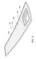
- FIG. 7illustrates a cross-sectional view of an in-molded resistive element including formed film layer including one or more conductive ink traces.
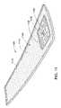
- FIG. 8depicts a cross-sectional view of an in-molded electromagnetic shielding element including a formed film layer.
- FIG. 9illustrates an exploded view of an article of manufacture incorporating a film having a resistive element, an electromagnetic shielding element, and/or a film switch printed on the film.
- FIG. 10illustrates an article of manufacture including a cellular antenna and an in-molded electromagnetic shielding element.
- FIG. 11depicts an article of manufacture including an RFID antenna and an in-molded electromagnetic shielding element.
- the present disclosurerelates to in-molded switch devices.
- the preferred embodimentis directed to capacitive switches which may be in-molded.
- the capacitive switchesmay also be in-molded as three dimensional structures.
- capacitive switchingdetects changes in capacitance due to a disturbance that defines a switching event.
- the present disclosurefurther relates to in-molded resistive and shielding elements.
- the sensing zone's capacitancewhen a conductive or charged object, such as a finger, is placed near a sensing zone, the sensing zone's capacitance changes, indicating the occurrence of a switching event.
- the sensing zone's capacitance changesare detected by sensing circuitry.
- the sensing circuitrycan be tuned to detect specific changes in capacitance.
- the sensing circuitrycan be tuned to detect the presence of a finger proximal a sensing zone, while not detecting other types of disturbances (e.g., moisture). Examples of capacitive switch sensing electronics are disclosed in, for example, U.S. Pat. No. 5,972,623 to Gupta et al., filed Oct.
- the capacitive switchesmay be used to detect an object at a distance as well as a touch. These sensing operations are described in detail with respect to U.S. Pat. Nos. 5,730,165, 6,288,707, 6,377,009, 6,452,514, 6,457,355, 6,466,036, 6,535,200, the entire contents of which are incorporated by reference herein.
- the switchcan be advantageously contoured to a desired shape.
- Such in-molded capacitive switcheshave numerous applications.
- the switchescan be used in numerous automotive interior applications such as center stack consoles (e.g., radio switches, HVAC switches, navigation switches, heated seat switches, etc.).
- the switchescan be molded to appear flat (like a touch panel,) indented (to direct the user to the switch), or to look like a rotary knob (protruding outward from the surface).
- the in-molded capacitive switches described hereincan be used in overhead consoles (e.g., sunroof, map light, homelike switches), door trim (e.g., window and heated seat switches). Depending on the application, it may be preferable to take steps to ensure that the switch can not accidentally be activated by touch alone.
- Other applicationsinclude exterior lighting switches on a vehicle instrument panel, A-pillar trim switches for operating power liftgates and liftglass, B-pillar switches for keyless entry appliqués and interior illumination (once the keyless entry is activated).
- Other applicationsmay include switches to control accessories (such as an IPOD®) that may be included, for example, in the center console as a flip out module.
- Typical door latchescontain several switch functions (i.e. door ajar, door open, child security, O/S lock/unlock, I/S lock).
- switch functionsi.e. door ajar, door open, child security, O/S lock/unlock, I/S lock.
- these connectionsare made with metal stampings, which lend themselves well to the application.
- metal stampingswhich lend themselves well to the application.
- switches and varying latch cover plastic thicknessesit can become rather difficult to route these connections.
- the interconnection system used in these applicationscould be replaced with printed conductive ink conductors. The use of conductive ink traces makes it simpler to route the conductors in areas where it was not possible before.
- the switches described hereinmay be used with appliances with touch type switch panels (i.e. microwaves, stoves, refrigerators, washers, dryers, blenders, tasters).
- Other examplesmay include consumer electronics such as music players or laptop computers where the switches may be in-molded with the plastic housings of such devices.
- the in-molded switch conceptlends itself especially well to these applications given the trend to providing more rounded edges and three dimensional shapes. In addition, these switches will not wear out over time like a membrane or dome type switch array.
- a three-dimensional molded partis created which includes one or more of the following features:
- such three-dimensional shapescan have several surfaces, where the surfaces are either flat, curved or a combination of both.
- the methodcomprises preparing a film switch by printing a conductive ink sensing zone on a formable film, forming the film to a desired shape, die-cutting the formed film, inserting the formed film in an injection mold, and introducing a molten plastic material into the mold.
- FIG. 1an exploded view of a film comprising a film switch 20 is described.
- film switch 20comprises a film 22 on which a variety of ink layers are printed.
- the embodiment of FIG. 1is directed to a keyless vehicle entry system.
- Film 22comprises a sheet of formable film.
- Exemplary films that are suitable for use as film 22include polycarbonate-based Makrofol® and Bayfol® films supplied by Bayer Films Americas of Berlin, Conn.
- the color, translucence, and/or transparency of film 22may be selected based on the desired application.
- film 22is a smoked black color that is preferably translucent and which allows graphic indicia printed on one side to be viewed on the other side.
- FIG. 1several layers of various inks 24 , 26 , 28 , 30 , 32 , 34 , and 36 are printed on film 22 to give the part its decorative appearance, to provide the graphics for the keyless functions, and to provide the conductive switches (electrodes) for activation by a user.
- a wide variety of printing processesmay be used to deposit the various ink layers, including without limitation screen printing, off-set printing, gravure printing, flexographic printing, pad printing, intaglio printing, letter press printing, ink jet printing, and bubble jet printing.
- screen printingis preferred.
- ink layer 24is applied to film 22 using a printing process as described above.
- Ink layer 24preferably includes inkless areas that define graphic indicia 38 related to the desired switching function. Since the embodiment of FIG. 1 is directed to keyless entry systems, the inkless areas 38 preferably define alpha-numeric characters.
- a layer of white translucent ink 26is printed on top of inkless area 38 to give the graphic indicia a white appearance. Of course, other colors may be used if desired.
- Suitable inks for forming ink layers 24 and 26include without limitation Noriphan® HTR, a solvent-based, one-component screen printing ink based on a high temperature resistant thermoplastic resin which is supplied by Pröll KG of Germany, and Nazdar® 9600 Series inks with 3% catalyst, which are supplied by the Nazdar Company of Shawnee, Kans.
- Ground layer 28provides a barrier for the switch (electrode) traces to ensure that inadvertent actuations do not occur by accidentally touching a trace.
- the conductive ink used in ground layer 28 and the other conductive ink layersis preferably formulated to withstand forming processes wherein film 22 is formed into a desired shape.
- the conductive inkis also preferably formulated to withstand typical injection molding temperatures and blow-off.
- One suitable conductive inkis DuPont Silver Conductor 5096 , which is designed for use in thermoforming operations or where extreme crease conditions are employed on flexible substrates.
- Another example of a conductive inkis Electrodag® SP-405 available from Acheson. Colloids Company.
- Ground or shield layer 28includes a plurality of unprinted (inkless) areas 40 that define apertures which are sized to accommodate conductive ink sensing zones 42 (discussed below).
- Dielectric layer 30is printed on ground layer 28 using a dielectric ink that is formulated to withstand the film forming and molding processes described below. Dielectric layer 30 is preferably configured to cover the entire ground layer 28 and insulates conductive ink sensing zones 42 and their associated electrodes from ground layer 28 .
- Switch layer 32is then printed on dielectric layer 30 .
- Switch layer 32is formed from a conductive ink of the type described above with respect to ground layer 28 .
- Switch layer 32also comprises a plurality of sensing zones 42 which sense the presence of an object, finger, etc. at different locations. As shown in the figure, sensing zones 42 are preferably aligned in correspondence with one of the indicia 38 so that a user's selection of a particular one of the indicia is detected by a corresponding one of the sensing zones 42 .
- Switch layer 32also comprises a plurality of electrode traces 44 , 46 , 48 , 50 , and 52 which allow each sensing zone 42 to be connected to a sensing circuit (not shown).
- film switch 20may include one or more LEDs to illuminate regions of film switch 20 .
- LEDs(not shown) are provided to backlight each of the sensing zones 42 and graphic indicia 38 .
- LEDsare especially helpful to allow the car owner to see the indicia 38 at night.
- LEDsmay also be activated in response the presence of a finger or object near film switch 20 so that as a person begins to execute keystrokes necessary to unlock the doors, graphic indicia 38 will become illuminated.
- the LEDsmay have their own dedicated sensing zone, or they may be activated in response to a switching event at one or more of the sensing zones 42 .
- dielectric layer 34is preferably printed on switch layer 32 using a dielectric ink to electrically isolate the LED circuit from the switch circuit (i.e., sensing zones 42 and electrodes 44 , 46 , 48 , 50 , and 52 ).
- the film 22preferably remains substantially flat during the printing of ink layers 23 and 24 .
- the conductive layermay be removed from the print layers stack-up.
- layersmay be eliminated by combining layers such as the electrode and LED layers.
- film switch 20is prepared, it is preferably formed to a desired shape and size. The desired shape is preferably selected based on the structure into which it will be incorporated. Thus, for example, if the film switch 20 is to be used on a vehicle A-pillar, it is preferably formed to have shape that conforms to the A.-pillar shape.
- switch 20is shaped by thermoforming (vacuum) or pressure forming such as Niebling HPF (high pressure forming) or hydroforming.
- thermoformingvacuum
- pressure formingis preferred.
- vacuum thermoformingmay be suitable.
- a moldIn a vacuum thermoforming process, a mold is provided that defines the desired film shape.
- the moldmay comprise cavities and/or raised portions to define recessed surfaces and protruding surfaces, respectively, in the film.
- the filmis then clamped in a frame and heated. Once a rubbery state is achieved (e.g., flexible, softened, supple, and the like), the film is placed over the mold cavity. Air is then removed from the cavity via a vacuum, such that atmospheric pressure forces the film against the walls of the mold.
- Typical vacuum thermoforming temperaturesare generally from about 180° C. to about 200° C. with a temperature of about 190° C. being preferred.
- Typical vacuum thermoforming pressuresare about 1 Bar.
- film 22comprises a polycarbonate sheet.
- typical forming parametersinclude a pressure of about 35 Bar, a temperature of about 160 to 180° C., a maximum draw depth of about 35-40 mm, and an elongation ratio of about 3:1 to about 4:1.
- the form toolis preferably designed to create a part where decorative features are visible on the A-surface of film 22 .
- the decorative featuresare printed on the B-surface of film 22 and are visible on the A-surface.
- the decorative featuresmay be printed on the A-surface of film 22 .
- a positive (i.e., male or protruding) toolas opposed to a negative (i.e., female or cavity) tool in the film forming process to avoid contact between the film's A-surface and the tool surface, which can produce marks and surface wear on film 22 .
- a negative toolcan be used in the forming process instead.
- the cycle times, temperatures, and vacuum or pressuresare preferably adjusted accordingly to ensure the part does not exhibit any cracking of inks or excessive stretching.
- a diaphragm face of unpressurized fluidcomes into contact with the film surface.
- the diaphragmis contained within a frame that is matched to an embossing die (male tool).
- the fluidis pressurized, which forms the film into the desired shape based on the male tool on the other side of the film.
- the diaphragmagain is depressurized and the film can be released from the tool.
- the cycle times, temperatures, and pressuresare preferably adjusted accordingly to ensure the part does not exhibit any cracking of inks or excessive stretching.
- FIG. 2AAn embodiment of a film switch 20 after the forming operation is depicted in FIG. 2A .
- film switch 20includes a contoured region 54 that is produced by the forming operation.
- FIG. 2Ais a view of the “B-surface” of film switch 20 , i.e., the surface that faces away from a user when film switch 20 is molded in a support structure.
- ink layers 23are also contoured.
- film switch 20is then cut to the desired shape. In an exemplary process, die cutting is used (e.g., using a column guided punching tool with a male and female die set).
- FIG. 2Billustrates another embodiment of a film switch 20 including a contoured region 54 after the forming operation. Instead of showing the printed layers flowing up and over the edge of the formed part, as depicted in FIG. 2A , for the method of inserting the connector into the molded part (described in more detail below with respect to a switch tail configuration) the conducive layers of ink layers 23 are not printed up over the formed edge to be die cut.
- film switch 20is a thermoplastic material which is molded with heat and pressure into a shape via an injection molding process.
- Typical molding parametersvary based on the resins being molded. However, some examples of molding parameters are provided.
- urethanese.g., thermoplastic urethane or “TPU”
- typical injection molding pressuresrange from about 5,000 to about 8,000 PSI and the molding temperature ranges from about 380 to about 410° F.
- polycarbonatestypical injection molding pressures range from about 8,000 to about 15,000 PSI and the molding temperature ranges from about 540 to about 580° F.
- each materialmay have preferred molding pressures or temperatures outside of the exemplary ranges provided.
- thermoplastic materialsmay be used, including but not limited to polycarbonates, acrylonitrile-butadiene-styrene (“ABS”) polymers, and polycarbonate blends such as polycarbonate-ABS, polycarbonate-polybutylene terephthalate, and polycarbonate-polyethylene terephthalate.
- ABSacrylonitrile-butadiene-styrene
- polycarbonate blendssuch as polycarbonate-ABS, polycarbonate-polybutylene terephthalate, and polycarbonate-polyethylene terephthalate.
- Specific examples of the foregoing polycarbonate blendsare those sold under the Makrolon® name by Bayer Films Americas.
- the thermoplastic resinpreferably has a melt flow index of greater than about 20 as measured by the ISO 1133 or ASTM D-1238 procedures.
- film 22comprises a polycarbonate film and the thermoplastic comprises Makrolon® 2405, which has an ASTM D-1238 melt flow index (300° C./1.2 kg) of 20.
- Exemplary thermoplastic urethanesinclude Texin® thermoplastic urethanes supplied by Bayer MaterialScience LLC of Pittsburgh, Pa.
- One exemplary Texin® materialis Texin® 245.
- Exemplary ABS materialsinclude ABS materials supplied by Lanxess Deutschland GmbH. Two exemplary ABS materials supplied by Lanxess are Lustrant® LGA and Lustran® LGA-SF.
- acrylic materialssuch as Plexiglas® V052 a product of Altuglas International of Philadelphia, Pa. may be used.
- the thermoplastic materialbonds well directly with the film.
- an adhesion promotermay be required for improved bonding with the film.
- a mold(not shown) which is configured to accept and retain film switch 20 .
- the moldpreferably comprises two halves (shells) that can be mated to define a mold cavity in which molten thermoplastic is injected.
- the mold cavitydefines the shape of the part being formed.
- One of the mold halvesis stationary and one is movable.
- Film switch 20is preferably disposed in the stationary mold half and held in place by a press fit as the mold halves are mated prior to introducing the molten plastic.
- the stationary mold halfis preferably configured to retain film switch 20 such that the thermoplastic material can flow over it to yield part in which some or all of the A-surface (user-facing surface) of film switch 20 exposed.
- the graphics, sensing zones, and electrodesare less than 0.5 mm behind the exposed A-surface of film switch 20 .
- Film switch 20is preferably disposed in the mold such that printed ink layers 23 and 24 ( FIG. 1 ) face into the mold interior without contacting the mold surfaces. This process advantageously produces a finished support structure that allows the user to directly contact film switch 20 , while still protecting the ink layers 23 and 24 from direct exposure to the environment.
- the A-surface of the finished partwill appear to contain all the decorative features such as switch graphics, simulated wood grain, chrome or other smooth or textured surfaces.
- these graphicswill actually be on the B-surface of the film, with the switch circuit printed directly behind the graphic indicia portions. While it is preferable to locate the ink components on the B-surface of film switch 20 , in certain embodiments the ink components may be located on the A-surface to face the user in an installed condition.
- connector terminalsare provided to allow the in-molded capacitive switch to be removably connected to sensing electronics or other electronic devices.
- the terminalsare preferably designed to match the contoured, three dimensional shape of the B-surface of film switch 20 .
- Each terminalis placed in the “moving side” of the injection mold.
- the terminal endspress fit into receiver pockets in the mold. This step may be completed as a hand or robotic process.
- Locationmay be established by a pocket in the moving mold half and a locator pin (this can also be an ejector pin).
- a pressure zone(adhered to the terminal in advance) is another option for keeping the terminal in place.
- a thin film (bead) of any type of conductive adhesivei.e. silver filled epoxy
- conductive adhesivei.e. silver filled epoxy
- the application of the conductive adhesivemay be completed by hand or robotically automated.
- An example of conductive adhesiveis CHO-BOND® 584 (available from Chomerics) which combines the adhesive properties of epoxy with the conductivity of silver.
- Another method for insuring terminal attachmentis using a B-stageable conductive epoxy that is printed over the conductive traces in the printing process.
- the injection moldAfter applying the conductive adhesive to the connector terminals, the injection mold is closed and the normal injection molding sequence ensues to cause the selected thermoplastic material to flow into the mold cavity defined by the two mold halves.
- the terminals and conductive epoxyare pressed onto the silver ink traces 44 , 46 , 48 , 50 , and 52 on film switch 20 .
- Careful stepsshould be taken to ensure that the injection molding process does not force the conductive epoxy to inadvertently flow into unwanted areas.
- the heat of the injection molding processactually cures the conductive epoxy in a short time frame (at room temperature this process could take up to 24 hours).
- the partis then ejected from the mold. As a result of this process, the thermoplastic material holds the terminals in place.
- connectorcan be molded directly into the plastic part.
- a terminal blockmay also be provided.
- multiple terminalsare pre-molded into a terminal block, and the block is then molded into the part.
- the terminal blockwill have a substantially flat surface that is connected to conductive ink traces 44 , 46 , 48 , 50 , and 52 .
- a terminal blockmay also be provided wherein individual terminals protrude from the block to connect to the conductive ink traces.
- An exemplary terminal block that is suitable for this embodimentis a BergStik® Unshrouded Header 54201 connector supplied by FCI of Etters, Pa. The same methods of attaching a terminal block as previously described apply here (e.g., using conductive epoxy).
- terminal connectorscan be permanently fixed in place via an injection molding process, minimizing the possibility of their becoming unattached from the silver ink through the conductive adhesive.
- the previously described molding processminimizes the likelihood of the conductive epoxy cracking, which could degrade its performance.
- the conductive adhesiveis cured quickly due to the heat transfer of the injection molding process. Normally, conductive adhesives such as epoxies are cured at room temperature or through infrared or ultrasonic curing methods. However, they quickly cure at common injection molding temperatures, such as those described previously.
- a flat flexible cablee.g., a wraparound film switch tail or “pig-tail” may also be used to connect switch layer 32 to sensing circuitry or other electronic components.
- a flat flexible cable connectoris an FCI 65801 Clincher Receptacle.
- the wrap-around switch tailis connected to conductive traces 44 , 46 , 48 , 50 , and 52 and is molded into the part so that a free end of the tail extends from the part for connection to the sensing circuitry or other electronic components.
- FIG. 2Billustrates the conducive layers of ink layers 23 inserted into the molded part as opposed to printed over the formed edge.
- FIG. 4depicts a cross-sectional view of a molded part 56 including a capacitive switch.
- connector terminal 60is attached to one of the conductive ink traces 44 , 46 , 48 , 50 , 52 ( FIG. 1 ) via a conductive adhesive 61 .
- Molded plastic 58surrounds a portion of connector terminal 60 , thereby securely retaining it in molded part 56 .
- a female connector housingmay be incorporated into the molded part to avoid the use of terminals that protrude from the part.
- a mating connectoris removably attached to the molded part after the molding process is complete.
- the mating connectoris an individual component, while in other embodiments it is incorporated into an electronic module that includes the sensing circuitry for detecting switching events.
- the partmay be molded with voids that allow for subsequent attachment to connector terminals after the molding process.
- a close-outis provided in the injection mold to define voids in the part.
- the voidsare preferably in substantial alignment with conductive ink traces 44 , 46 , 48 , 50 , and 52 .
- the connector terminalsare inserted into the voids and in contact with the conductive ink traces 44 , 46 , 48 , 50 , and 52 . Any space around the connector terminals is then filled with a suitable plastic material to seal conductive ink traces 44 , 46 , 48 , 50 , and 52 .
- a conductive adhesive of the type described previouslymay also be used to connect the terminals to the conductive ink traces 44 , 46 , 48 , 50 , and 52 .
- FIG. 4shows molded part 56 from the backside (B-surface) to show how the terminals 60 are positioned.
- terminals 60may be located anywhere on the back of the part based on the application.
- the foregoing processavoids the need for providing separate graphic overlays to protect sensing zones 42 and associated electrodes 44 , 46 , 48 , 50 , and 52 .
- the electrodes and sensing zonescan be more consistently positioned at equal distances from the front surface of the article, thereby reducing variations in sensitivity amongst the individual sensing zones and electrodes.
- all of the switch elements including the electrodes and conductorsare protected from environmental concerns (i.e. humidity, salt exposure). Insert molding the connector terminals 60 and sealing off directly around them minimizes these environmental issues.
- LED'smay be directly mounted on the conductive traces 44 , 46 , 48 , 50 , 52 , and over-molded. However, it may be desired to provide a shut-off in the mold (leaving the conductive traces slightly exposed). In one embodiment, the LED would be attached using conductive epoxy or an equivalent method. The void in the mold could then be filled with thermally conductive epoxy to seal the LED. It may be also beneficial to mount the LED as a secondary process if the LED requires light piping to spread the light output to a wider output pattern. In this case the LED and light pipe (e.g., a light guide) assembly would be designed with leads that could be attached to the conductors. Another technique is to insert a light pipe that can assist in lighting multiple areas with one or more LED's. While this technique would require external connections to the LED's, it may prove cost beneficial.
- FIG. 3An embodiment of an LED incorporated into a part with an in-molded capacitive switch is shown in FIG. 3 , wherein LED 63 is molded into part 56 .
- a typical LED that would be suitableis an Osram type “point LED” part number LW P473. Modification to the packaging of the LED may be required to ensure proper light output through the film and switch logos. These types of LED's typically draw 15 mA or less which allows for encasing them in plastic resin without overheating the component or the switch packaging. However, as mentioned previously, an alternative to totally sealing them is to leave a void in the backside of the molded part 56 where each LED is located to dissipate the heat.
- the voidis made, for example, by including a core pin shut-off in the mold that mates with the B-surface of the film. This area could then be sealed with a thermally conductive epoxy which would prevent water intrusion.
- the process for the attachment to the conductors of such LED'swould be similar to the terminal attachment described in this section. Parts such as the LED's may be, for example, hand inserted where pinpoint consistency of placement is not required. Alternatively, the LED's may be robotically inserted (such as using a pick and place machine) for precision or multiple component placement that would otherwise be too difficult or costly to perform using hand placement.
- in-molded capacitive switches described hereincan be used in a number of different configurations and geometries.
- conductors and electrodescan be formed into protruding or recessed shapes (for items such as knobs and buttons).
- the processes described hereinallow the switch components to be printed onto a flat film and then formed to the desired shape.
- multi-segment sensing zonescan be used.
- a molded knobis created which allows a user to operate a device such an HVAC system, radio, CD player, etc. by moving his fingers around the circumference of the knob.
- An embodiment of a knob with an in-molded capacitive switchis depicted in FIGS. 5 and 6 .
- Knob 62is a generally cylindrical structure that is preferably molded from a plastic material and which includes a user contact surface 65 for triggering switching events.
- Film switch 64generally comprises a series of printed ink layers on a film as described previously.
- FIG. 5depicts a plan view of film switch 64 with sensing zones 66 and electrodes 68 (ground layers, dielectric layers and graphic layers are not shown), prior to a forming operation.
- Sensing zones 66 and electrodes 68are printed using a conductive ink and printing process of the type described previously.
- Film switch 64is preferably formed to the desired knob shape using a suitable forming process such as vacuum thermoforming.
- film switch 64is preferably disposed in a stationary mold half such that the printed ink layers face into the mold cavity and avoid contact with the mold walls.
- the stationary mold halfpreferably defines a shape into which film switch 64 fits so that molten plastic may be injected over it.
- the ink layers that define sensing zones 66 and electrodes 68preferably face into the mold cavity and do not contact the mold surfaces.
- the user exposed surface (A-surface) of the resulting structurecomprises the A-surface of film switch 64 .
- sensing zones 66each define an L-shaped cross-section around the periphery of knob 62 .
- Knob 64is preferably stationary. However, it allows the user to simulate rotation by triggering different switching events as the user's fingers traverse the knob's circumference, which causes capacitance changes at each successive sensing zone 66 .
- connector terminalsmay be connected to electrode traces 68 via a conductive adhesive and molded into knob 64 to allow for removable connection to sensing circuitry or other electronics.
- FIG. 7illustrates a cross-sectional view of an in-molded resistive element part 74 including a formed film layer 70 on which one or more conductive ink traces 76 are printed.
- the formed film layer 70is overlaid on molded plastic part 78 such that the formed film layer 70 has one side exposed, a portion of one side exposed, or both sides are in-between the top and bottom of the molded plastic part 78 . Either side of the formed film layer 70 can face the interior of the molded plastic part 78 .
- either side of the film layer 70can be disposed to the exterior of the molded plastic part 78 .
- the A-surface or B-surface of the formed film layercan be disposed on the A-surface or B-surface of the molded plastic part 78 .
- connection point 72(i.e., an exposed area of conductive ink) is provided on the surface of the film. Connection point 72 can then be used to connect the resistive element to another device, circuit or component. Connections to connection point 72 can be made by, for example, a spring-clip connector, rivet connector, and the like. In addition, a pig-tail type connector as discussed above can by used as an alternative. Alternatively, connection point 72 can be used to connect other conductive ink traces on the same printed and formed film layer 70 (not shown). These additional traces can be printed on a layer separated by, for example, a non-conductive layer such as a dielectric layer.
- LEDscan be directly mounted on the conductive traces 76 and over-molded or surface-mounted using conductive epoxy, or an equivalent technique.
- the resistive element or trace designmay serve as a heating component or as an antenna.
- the resistive elementsmay be part of a circuit also formed of conductive ink, such as an RC circuit, where both the resistor and capacitor of the RC circuit are formed at least in part of conductive ink.
- Film switch 20 described above with respect to FIG. 1also can be printed on the same formed film layer 70 .
- a dielectric layercan be constructed on either the front or back surface of the formed filled layer 70 to provide a coating over some or the entire surface. This dielectric coating can be used to protect an exposed surface or to provide a non-conductive layer between two ink layers.
- the resistance of the conductive ink traces 76is based on the ohms/square inch of the conductive ink, the thickness of the conductive ink traces 76 and the width and length of the conductive ink traces.
- the conductive ink traces 76can thus be formed to provide different resistances.
- the resistive elementscan be used to provide a voltage drop to a device such as an LED.
- conductive ink traces 76may be arranged as a sine wave, a triangle, or zig-zag pattern.
- layout of conductive ink traces 76can be based upon the number of required connection points 72 , or whether the resistive elements are to be connected serially or in parallel.
- the conductive ink traces 76can be utilized to provide a tamper detection circuit, which detects a drop in voltage caused by a corresponding decrease in resistance of the in-molded resistive element 74 upon a break or puncture in film layer 70 .
- a resistive element 74can be designed to be tamper resistant, such that electrical connectivity is maintained if someone attempts to drill into or otherwise break or puncture the film layer 70 .
- the conductive ink traces 76can be used as heating elements. This configuration can be used to provide heat to, and thus control the temperature of, components affixed to or near the heating elements.
- an electromagnetic shielding element(or RF shield) is formed of conductive ink. Radiation of electromagnetic energy may be released from an electronic device. Some electronic devices generate sufficiently strong electromagnetic fields that propagate away from the device as to interfere with other electronic devices or otherwise cause problems. While radiated emissions are usually associated with non-intentional radiators, intentional radiators can also have unwanted emissions at frequencies outside their intended transmission frequency band. It is thus desirable to provide an electromagnetic shielding element to prevent radiation from exiting the device. Alternatively, it is desirable to provide an electromagnetic shielding element to prevent radiation from external sources from entering the device.
- Ground or shield layer 28 of FIG. 1may act as an electromagnetic shield. This property allows ground or shield layer 28 to inhibit the exit or entry of radiated emissions caused by electrical components within or outside of a device, respectively.
- FIG. 8depicts a cross-sectional view of an in-molded electromagnetic shield part 80 including formed film layer 82 on which conductive ink traces 86 arranged in a grid pattern are printed. As described above, the conductive ink traces 86 provide a shielding layer to inhibit the exit or entry radiated emissions.
- the formed film layer 82 containing conductive ink traces 86is shown completely covering a molded plastic part 88 .
- Either side of the film layer 82can be disposed to the interior or exterior of the molded plastic part.
- the A-surface or B-surface of the formed film layer 82can be disposed on the A-surface or B-surface of the molded plastic part 88 .
- formed film layer 82can be constructed to wrap around edges of molded plastic 88 , as shown in FIG. 8 .
- formed film layer 82may form an electromagnetic shield partially covering molded plastic 88 .
- the formed film layer 82also can be exposed, partially exposed or in-between the top and bottom of the molded plastic part 88 .
- a dielectric layercan be constructed on either the front or back surface of the formed film layer 82 to provide a coating over some or all of the surface. This dielectric coating can be used to protect an exposed surface or to provide a non-conductive layer between two ink layers.
- the pattern of the shielding element formed by conductive ink traces 86is a design choice.
- the conductive ink traces 86may be arranged in a grid pattern or as a solid sheet of ink.
- conductive ink traces 86can vary in thickness or in pattern throughout formed film layer 82 , to selectively inhibit radiation from different electromagnetic fields or at different frequencies or frequency bands, thereby creating different shielding footprints.
- connection point 84(i.e., an exposed area of conductive ink) is provided on the surface of the film.
- Connection point 84can be used to connect the shielding element to another device, circuit or component. Connections to connection point 84 can be made by, for example, a spring-clip connector, rivet connector, and the like. In addition, a pig-tail type connector as discussed above can by used as an alternative.
- connection point 84can be used to connect other conductive ink traces on the same printed and formed film layer 82 (not shown). These additional traces can be printed on a layer separated by, for example, a non-conductive layer such as a dielectric layer.
- FIG. 9illustrates an exploded view of an article of manufacture 74 incorporating a film 20 having a resistive element and a film switch printed on a layer on the film 20 (shown collectively as ink layer 90 ).
- Film 20can be inserted in a molded part 92 such that the printed ink layer faces into a mold cavity (or B-surface) and is not exposed after the molded part is formed.
- film 20can be inserted in molded part 92 such that the printed ink layer faces the other way and is exposed.
- either surface of film 20can be disposed on the A-surface (i.e., exterior) of the molded part 92 as described above.
- film 20can be inserted in-between the top and bottom of the molded part such that neither side is exposed or such that only a portion of the film is exposed. If necessary, the film can be inserted to avoid contact with the mold walls.
- conductive ink traces that form an electromagnetic shielding elementcan be substituted for the conductive ink traces that form the resistive element ( FIG. 7 , 76 ).
- Resistive element, switch and/or electromagnetic shielding elementalso can be printed on the same layer. Or, they can be formed of different ink layers, separated by a non-conductive layer such as a dielectric layer.
- resistive element 74(or electromagnetic shielding element 80 ) can be decorated with graphics, such as numbers, representative pictures, illustrations, and the like. Decoration of resistive element 74 or in-molded electromagnetic shielding element 80 may be accomplished utilizing various methods, including painting, laser etching, or other printing processes.
- resistive element 74 or electromagnetic shielding element 80may be accomplished by layering a decorated film layer on the front or back surface of resistive element 74 or electromagnetic shielding element 80 .
- Backlightingcan also be provided behind resistive element 74 or electromagnetic shielding element 80 .
- FIG. 10depicts an article of manufacture which serves as a cellular antenna and shielding element 1000 .
- the design of conductive ink tracesare printed on formed film layer 1010 to create a cellular antenna array 1002 and a shielding element 1000 .
- Both the cellular antenna array 1002 and the shielding element 1000can be constructed of the same ink layer or can be constructed of two separate ink layers separated by a non-conductive layer such a dielectric layer.
- the formed film layer 1010 of this embodimentis overlaid on molded plastic 1008 . Film layer 1010 can be inserted in molded part 1008 such that the printed ink layer faces into a mold cavity (or B-surface) and is not exposed after the molded part is formed.
- film layer 1010can be inserted in molded part 1008 such that the printed ink layer faces the other way and is exposed.
- film layer 1010can be inserted in-between the top and bottom of the molded part 1008 such that neither side is exposed or such that only a portion of the film is exposed.
- either the A-surface or the B-surface of film layer 1010can be disposed on the outside (or A-surface) of the molded plastic 1008 .
- electromagnetic shielding layer 1006may completely or partially, or not at all cover cellular antenna array 1002 on one or more sides.
- electromagnetic shielding layer 1006may completely or partially, or not at all cover cellular antenna array 1002 on one or more sides.
- Such a configurationcan be accomplished by printing the cellular antenna array 1002 and the electromagnetic shielding layer 1006 on different ink layers and separating them by a non-conducted layer such as a dielectric layer.
- the above-described shielding embodimentscan be configured to permit the cellular antenna array 1002 to radiate away from the device while protecting the circuits or persons on the other side of the array from that radiation.
- connection point 1004i.e., an exposed area of conductive ink
- connection point 1004can be used to connect the antenna and/or shielding element to another device, circuit or component. Connections to connection point 1004 can be made by, for example, a spring-clip connector, rivet connector, and the like. In addition, a pig-tail type connector as discussed above can by used as an alternative. Alternatively, connection point 1004 can be used to connect other conductive ink traces on the same printed and formed film layer 1010 (not shown). These additional traces can be printed on a layer separated by, for example, a non-conductive layer such as a dielectric layer.
- FIG. 11depicts an article of manufacture 1100 which serves as an RFID antenna 1106 and electromagnetic shielding layer 1108 .
- the RFID antenna 1106 and electromagnetic shielding layer 1108are constructed of conductive ink printed on a formed film layer 1112 and is attached to a passive RFID circuit 1104 .
- an electromagnetic shielding layer 1108is incorporated around the RFID antenna 1106 in this embodiment. This can be accomplished by printing one layer including both the electromagnetic shielding layer 1108 and the RFID antenna 1106 or by printing multiple layers separated a non-conductive layer such as a dielectric.
- connection point 1102i.e., an exposed area of conductive ink
- connection point 1102can be used to connect the RFID antenna and/or shielding element to another device, circuit or component.
- Connections to connection point 1004can be made by, for example, a spring-clip connector, rivet connector, and the like.
- a pig-tail type connectoras discussed above can by used as an alternative.
- connection point 1004can be used to connect other conductive ink traces on the same printed and formed film layer 1112 (not shown). These additional traces can be printed on a layer separated by, for example, a non-conductive layer such as a dielectric layer.
- Another shielding ink layercould be formed beneath the RFID antenna 1106 (not shown). This other shield would allow the RFID antenna 1106 to radiate away from the device while protecting the circuits or persons on the other side of the antenna from that radiation.
- Film layer 1112can be inserted in molded part 1110 such that the printed ink layer faces into a mold cavity (or B-side) and is not exposed after the molded part is formed.
- film layer 1010can be inserted in molded part 1110 such that the printed ink layer faces the other way and is exposed.
- film layer 1112can be inserted in-between the top and bottom of the molded part 1110 such that neither side is exposed or such that only a portion of the film is exposed.
- Either side of the film layer 1112can be disposed to the interior or exterior of the molded plastic part.
- the A-surface or B-surface of the formed film layer 1112can be disposed on the A-surface or B-surface of the molded plastic part 1110 .
- the electromagnetic shielding layer 1108may or may not be utilized.
- the electromagnetic shielding layer 1108may have an opening for the RFID antenna 1106 .
- electromagnetic shielding layermay completely cover RFID antenna 1106 .
Landscapes
- Engineering & Computer Science (AREA)
- Manufacturing & Machinery (AREA)
- Physics & Mathematics (AREA)
- Electromagnetism (AREA)
- Microelectronics & Electronic Packaging (AREA)
- Mechanical Engineering (AREA)
- Manufacture Of Switches (AREA)
- Push-Button Switches (AREA)
- Injection Moulding Of Plastics Or The Like (AREA)
- Shielding Devices Or Components To Electric Or Magnetic Fields (AREA)
- Details Of Resistors (AREA)
- Moulds For Moulding Plastics Or The Like (AREA)
- Blow-Moulding Or Thermoforming Of Plastics Or The Like (AREA)
- Switches That Are Operated By Magnetic Or Electric Fields (AREA)
Abstract
Description
Claims (32)
Priority Applications (19)
| Application Number | Priority Date | Filing Date | Title |
|---|---|---|---|
| US12/191,825US8198979B2 (en) | 2007-04-20 | 2008-08-14 | In-molded resistive and shielding elements |
| BRPI0822517-6ABRPI0822517A2 (en) | 2008-04-18 | 2008-09-17 | Manufacturing article, method for producing a manufacturing article, electromagnetic shielding, and resistive element |
| PCT/US2008/076670WO2009128856A1 (en) | 2008-04-18 | 2008-09-17 | In-molded resistive and shielding elements |
| KR1020157005503AKR20150038565A (en) | 2008-08-14 | 2008-09-17 | In-molded resistive and shielding elements |
| EP08873908AEP2286419A4 (en) | 2008-04-18 | 2008-09-17 | In-molded resistive and shielding elements |
| CN201310059184.4ACN103252867B (en) | 2008-04-18 | 2008-09-17 | Mould internal resistance element and shielding element |
| CN200880129510.1ACN102047352B (en) | 2008-04-18 | 2008-09-17 | In-mold resistive components and shielding components |
| JP2011504993AJP5548674B2 (en) | 2008-04-18 | 2008-09-17 | In-mold resistance element and in-mold shield element |
| KR1020107025908AKR101700926B1 (en) | 2008-04-18 | 2008-09-17 | In-molded resistive and shielding elements |
| KR1020157023325AKR101675793B1 (en) | 2008-04-18 | 2008-09-17 | In-molded resistive and shielding elements |
| US13/473,301US8461957B2 (en) | 2007-04-20 | 2012-05-16 | In-molded resistive and shielding elements |
| US13/897,715US9576755B2 (en) | 2007-04-20 | 2013-05-20 | In-molded resistive and shielding elements |
| US14/170,443US20140252671A1 (en) | 2007-04-20 | 2014-01-31 | In-molded resistive and shielding elements |
| US14/170,425US20140251782A1 (en) | 2007-04-20 | 2014-01-31 | In-molded resistive and shielding elements |
| US14/169,747US20140252670A1 (en) | 2007-04-20 | 2014-01-31 | In-molded resistive and shielding elements |
| US14/169,818US20140251781A1 (en) | 2007-04-20 | 2014-01-31 | In-molded resistive and shielding elements |
| US14/169,700US20140252688A1 (en) | 2007-04-20 | 2014-01-31 | In-molded resistive and shielding elements |
| US14/169,778US20140262722A1 (en) | 2007-04-20 | 2014-01-31 | In-molded resistive and shielding elements |
| JP2014102617AJP2014222655A (en) | 2008-04-18 | 2014-05-16 | In-molded resistive element and in-molded shielding element |
Applications Claiming Priority (3)
| Application Number | Priority Date | Filing Date | Title |
|---|---|---|---|
| US92542107P | 2007-04-20 | 2007-04-20 | |
| US12/106,250US8514545B2 (en) | 2007-04-20 | 2008-04-18 | In-molded capacitive switch |
| US12/191,825US8198979B2 (en) | 2007-04-20 | 2008-08-14 | In-molded resistive and shielding elements |
Related Parent Applications (1)
| Application Number | Title | Priority Date | Filing Date |
|---|---|---|---|
| US12/106,250Continuation-In-PartUS8514545B2 (en) | 2007-04-20 | 2008-04-18 | In-molded capacitive switch |
Related Child Applications (1)
| Application Number | Title | Priority Date | Filing Date |
|---|---|---|---|
| US13/473,301ContinuationUS8461957B2 (en) | 2007-04-20 | 2012-05-16 | In-molded resistive and shielding elements |
Publications (2)
| Publication Number | Publication Date |
|---|---|
| US20090108985A1 US20090108985A1 (en) | 2009-04-30 |
| US8198979B2true US8198979B2 (en) | 2012-06-12 |
Family
ID=41199379
Family Applications (9)
| Application Number | Title | Priority Date | Filing Date |
|---|---|---|---|
| US12/191,825Expired - Fee RelatedUS8198979B2 (en) | 2007-04-20 | 2008-08-14 | In-molded resistive and shielding elements |
| US13/473,301Expired - Fee RelatedUS8461957B2 (en) | 2007-04-20 | 2012-05-16 | In-molded resistive and shielding elements |
| US13/897,715Expired - Fee RelatedUS9576755B2 (en) | 2007-04-20 | 2013-05-20 | In-molded resistive and shielding elements |
| US14/169,700AbandonedUS20140252688A1 (en) | 2007-04-20 | 2014-01-31 | In-molded resistive and shielding elements |
| US14/169,778AbandonedUS20140262722A1 (en) | 2007-04-20 | 2014-01-31 | In-molded resistive and shielding elements |
| US14/170,443AbandonedUS20140252671A1 (en) | 2007-04-20 | 2014-01-31 | In-molded resistive and shielding elements |
| US14/170,425AbandonedUS20140251782A1 (en) | 2007-04-20 | 2014-01-31 | In-molded resistive and shielding elements |
| US14/169,747AbandonedUS20140252670A1 (en) | 2007-04-20 | 2014-01-31 | In-molded resistive and shielding elements |
| US14/169,818AbandonedUS20140251781A1 (en) | 2007-04-20 | 2014-01-31 | In-molded resistive and shielding elements |
Family Applications After (8)
| Application Number | Title | Priority Date | Filing Date |
|---|---|---|---|
| US13/473,301Expired - Fee RelatedUS8461957B2 (en) | 2007-04-20 | 2012-05-16 | In-molded resistive and shielding elements |
| US13/897,715Expired - Fee RelatedUS9576755B2 (en) | 2007-04-20 | 2013-05-20 | In-molded resistive and shielding elements |
| US14/169,700AbandonedUS20140252688A1 (en) | 2007-04-20 | 2014-01-31 | In-molded resistive and shielding elements |
| US14/169,778AbandonedUS20140262722A1 (en) | 2007-04-20 | 2014-01-31 | In-molded resistive and shielding elements |
| US14/170,443AbandonedUS20140252671A1 (en) | 2007-04-20 | 2014-01-31 | In-molded resistive and shielding elements |
| US14/170,425AbandonedUS20140251782A1 (en) | 2007-04-20 | 2014-01-31 | In-molded resistive and shielding elements |
| US14/169,747AbandonedUS20140252670A1 (en) | 2007-04-20 | 2014-01-31 | In-molded resistive and shielding elements |
| US14/169,818AbandonedUS20140251781A1 (en) | 2007-04-20 | 2014-01-31 | In-molded resistive and shielding elements |
Country Status (7)
| Country | Link |
|---|---|
| US (9) | US8198979B2 (en) |
| EP (1) | EP2286419A4 (en) |
| JP (2) | JP5548674B2 (en) |
| KR (3) | KR20150038565A (en) |
| CN (2) | CN103252867B (en) |
| BR (1) | BRPI0822517A2 (en) |
| WO (1) | WO2009128856A1 (en) |
Cited By (11)
| Publication number | Priority date | Publication date | Assignee | Title |
|---|---|---|---|---|
| US20140251782A1 (en)* | 2007-04-20 | 2014-09-11 | T-Ink, Inc. | In-molded resistive and shielding elements |
| US9057184B2 (en) | 2011-10-19 | 2015-06-16 | Delta Faucet Company | Insulator base for electronic faucet |
| US9074357B2 (en) | 2011-04-25 | 2015-07-07 | Delta Faucet Company | Mounting bracket for electronic kitchen faucet |
| US9243756B2 (en) | 2006-04-20 | 2016-01-26 | Delta Faucet Company | Capacitive user interface for a faucet and method of forming |
| US9333698B2 (en) | 2013-03-15 | 2016-05-10 | Delta Faucet Company | Faucet base ring |
| US9499128B2 (en) | 2013-03-14 | 2016-11-22 | The Crawford Group, Inc. | Mobile device-enhanced user selection of specific rental vehicles for a rental vehicle reservation |
| US9831872B1 (en) | 2016-08-17 | 2017-11-28 | Ford Global Technologies, Llc | Stationary control knob having proximity sensors |
| US20180110126A1 (en)* | 2013-09-27 | 2018-04-19 | Tactotek Oy | Method for manufacturing an electromechanical structure and an arrangement for carrying out the method |
| US10393363B2 (en) | 2017-04-25 | 2019-08-27 | Delta Faucet Company | Illumination device for a fluid delivery apparatus |
| US10698429B2 (en) | 2006-04-20 | 2020-06-30 | Delta Faucet Company | Electronic user interface for electronic mixing of water for residential faucets |
| US11478967B2 (en)* | 2018-08-02 | 2022-10-25 | Commissariat A L'energie Atomique Et Aux Energies Alternatives | Method for manufacturing a plastic part forming a human-machine control interface |
Families Citing this family (110)
| Publication number | Priority date | Publication date | Assignee | Title |
|---|---|---|---|---|
| WO2009150546A2 (en)* | 2008-06-10 | 2009-12-17 | Johnson Controls Technology Company | Capacitive switch sensors on decorative in-mold films background |
| US7928326B2 (en)* | 2009-02-27 | 2011-04-19 | Hewlett-Packard Development Company, L.P. | Thermoformed EMI shield |
| US20110120763A1 (en)* | 2009-11-21 | 2011-05-26 | Paragon Technologies Co., Ltd. | Structure and method of forming a film that both prevents electromagnetic interference and transmits and receives signals |
| US8330385B2 (en)* | 2010-02-15 | 2012-12-11 | Ford Global Technologies, Llc | Light bar |
| US8629364B2 (en) | 2010-03-01 | 2014-01-14 | Visteon Global Technologies, Inc. | Method for implementing capacitive sensing in the presence of conductive decorative materials |
| US8283800B2 (en) | 2010-05-27 | 2012-10-09 | Ford Global Technologies, Llc | Vehicle control system with proximity switch and method thereof |
| EP2395572A1 (en) | 2010-06-10 | 2011-12-14 | Bayer MaterialScience AG | Layer construction comprising electronic components |
| US20120043888A1 (en)* | 2010-08-18 | 2012-02-23 | Salter Stuart C | Vehicle Interior Light Configured to Color Correct and Method Thereof |
| US8454181B2 (en) | 2010-08-25 | 2013-06-04 | Ford Global Technologies, Llc | Light bar proximity switch |
| US8575949B2 (en) | 2010-08-25 | 2013-11-05 | Ford Global Technologies, Llc | Proximity sensor with enhanced activation |
| DE102010048237B4 (en)* | 2010-10-12 | 2012-08-30 | Diehl Ako Stiftung & Co. Kg | Operating device for a household electrical appliance |
| US10571772B2 (en) | 2011-01-11 | 2020-02-25 | Ajjer, Llc | Added feature electrooptical devices and automotive components |
| US20120292401A1 (en)* | 2011-05-18 | 2012-11-22 | Nuventix Inc. | Power Delivery to Diaphragms |
| US8975903B2 (en) | 2011-06-09 | 2015-03-10 | Ford Global Technologies, Llc | Proximity switch having learned sensitivity and method therefor |
| US8928336B2 (en) | 2011-06-09 | 2015-01-06 | Ford Global Technologies, Llc | Proximity switch having sensitivity control and method therefor |
| JP2012254564A (en)* | 2011-06-09 | 2012-12-27 | Sakaiya:Kk | Synthetic resin molded article having electrode terminal and metal thin film |
| US8804344B2 (en) | 2011-06-10 | 2014-08-12 | Scott Moncrieff | Injection molded control panel with in-molded decorated plastic film |
| US10004286B2 (en) | 2011-08-08 | 2018-06-26 | Ford Global Technologies, Llc | Glove having conductive ink and method of interacting with proximity sensor |
| JP5914142B2 (en) | 2011-09-14 | 2016-05-11 | タイコエレクトロニクスジャパン合同会社 | Conductive member and conductive member assembly |
| US9143126B2 (en) | 2011-09-22 | 2015-09-22 | Ford Global Technologies, Llc | Proximity switch having lockout control for controlling movable panel |
| KR101479892B1 (en)* | 2011-10-18 | 2015-01-06 | 피셔 테크놀로지 피티이. 엘티디. | A method of moulding |
| US10112556B2 (en) | 2011-11-03 | 2018-10-30 | Ford Global Technologies, Llc | Proximity switch having wrong touch adaptive learning and method |
| US8994228B2 (en) | 2011-11-03 | 2015-03-31 | Ford Global Technologies, Llc | Proximity switch having wrong touch feedback |
| US8878438B2 (en) | 2011-11-04 | 2014-11-04 | Ford Global Technologies, Llc | Lamp and proximity switch assembly and method |
| JP5314773B2 (en)* | 2012-02-10 | 2013-10-16 | ホシデン株式会社 | Component module |
| JP5868721B2 (en)* | 2012-02-10 | 2016-02-24 | ホシデン株式会社 | Input device |
| JP5753501B2 (en)* | 2012-02-10 | 2015-07-22 | ホシデン株式会社 | Component module |
| US9065447B2 (en) | 2012-04-11 | 2015-06-23 | Ford Global Technologies, Llc | Proximity switch assembly and method having adaptive time delay |
| US9559688B2 (en) | 2012-04-11 | 2017-01-31 | Ford Global Technologies, Llc | Proximity switch assembly having pliable surface and depression |
| US9568527B2 (en) | 2012-04-11 | 2017-02-14 | Ford Global Technologies, Llc | Proximity switch assembly and activation method having virtual button mode |
| US9531379B2 (en) | 2012-04-11 | 2016-12-27 | Ford Global Technologies, Llc | Proximity switch assembly having groove between adjacent proximity sensors |
| US9831870B2 (en) | 2012-04-11 | 2017-11-28 | Ford Global Technologies, Llc | Proximity switch assembly and method of tuning same |
| US9944237B2 (en) | 2012-04-11 | 2018-04-17 | Ford Global Technologies, Llc | Proximity switch assembly with signal drift rejection and method |
| US9660644B2 (en) | 2012-04-11 | 2017-05-23 | Ford Global Technologies, Llc | Proximity switch assembly and activation method |
| US8933708B2 (en) | 2012-04-11 | 2015-01-13 | Ford Global Technologies, Llc | Proximity switch assembly and activation method with exploration mode |
| US9520875B2 (en) | 2012-04-11 | 2016-12-13 | Ford Global Technologies, Llc | Pliable proximity switch assembly and activation method |
| US9184745B2 (en) | 2012-04-11 | 2015-11-10 | Ford Global Technologies, Llc | Proximity switch assembly and method of sensing user input based on signal rate of change |
| US9197206B2 (en) | 2012-04-11 | 2015-11-24 | Ford Global Technologies, Llc | Proximity switch having differential contact surface |
| US9287864B2 (en) | 2012-04-11 | 2016-03-15 | Ford Global Technologies, Llc | Proximity switch assembly and calibration method therefor |
| US9219472B2 (en) | 2012-04-11 | 2015-12-22 | Ford Global Technologies, Llc | Proximity switch assembly and activation method using rate monitoring |
| US9136840B2 (en) | 2012-05-17 | 2015-09-15 | Ford Global Technologies, Llc | Proximity switch assembly having dynamic tuned threshold |
| US8981602B2 (en) | 2012-05-29 | 2015-03-17 | Ford Global Technologies, Llc | Proximity switch assembly having non-switch contact and method |
| CN104349883B (en) | 2012-05-30 | 2016-06-29 | 日本写真印刷株式会社 | Injection molded article and its manufacturing method |
| US9337832B2 (en) | 2012-06-06 | 2016-05-10 | Ford Global Technologies, Llc | Proximity switch and method of adjusting sensitivity therefor |
| JP5990044B2 (en)* | 2012-06-25 | 2016-09-07 | 小島プレス工業株式会社 | In-vehicle sensor panel |
| US9641172B2 (en) | 2012-06-27 | 2017-05-02 | Ford Global Technologies, Llc | Proximity switch assembly having varying size electrode fingers |
| JP2014014587A (en)* | 2012-07-11 | 2014-01-30 | Panasonic Corp | Operation display device for washing machine |
| JP5484529B2 (en)* | 2012-08-07 | 2014-05-07 | ホシデン株式会社 | Component module and component module manufacturing method |
| JP5525574B2 (en)* | 2012-08-07 | 2014-06-18 | ホシデン株式会社 | Component module and component module manufacturing method |
| US8922340B2 (en) | 2012-09-11 | 2014-12-30 | Ford Global Technologies, Llc | Proximity switch based door latch release |
| CN103717044B (en)* | 2012-09-29 | 2018-05-22 | 深圳光启创新技术有限公司 | A kind of absorbing material |
| US8796575B2 (en) | 2012-10-31 | 2014-08-05 | Ford Global Technologies, Llc | Proximity switch assembly having ground layer |
| US9311204B2 (en) | 2013-03-13 | 2016-04-12 | Ford Global Technologies, Llc | Proximity interface development system having replicator and method |
| WO2015019126A1 (en)* | 2013-08-05 | 2015-02-12 | Diehl Ako Stiftung & Co. Kg. | Printed capacitive touch screen on a molded substrate and having non-flush reverse mounted leds |
| JP2015059706A (en)* | 2013-09-19 | 2015-03-30 | ダイキン工業株式会社 | Electric stove |
| US9945818B2 (en) | 2014-02-23 | 2018-04-17 | Qualcomm Incorporated | Ultrasonic authenticating button |
| US20150257278A1 (en)* | 2014-03-06 | 2015-09-10 | Tactotek Oy | Method for manufacturing electronic products, related arrangement and product |
| DE202014101407U1 (en)* | 2014-03-26 | 2015-06-29 | Rehau Ag + Co | Profile and electrical circuit arrangement with at least one such profile |
| AU2015247969A1 (en)* | 2014-04-14 | 2016-12-01 | Mobile Dynamic Marketing, Inc. | RFID shielding |
| US20150296608A1 (en)* | 2014-04-14 | 2015-10-15 | Mobile Dynamic Marketing, Inc. | Rfid shielding |
| DE102014106585A1 (en)* | 2014-05-09 | 2015-11-12 | Leonhard Kurz Stiftung & Co. Kg | Multilayer body and method for its production |
| WO2015179730A1 (en) | 2014-05-22 | 2015-11-26 | Tk Holdings Inc. | Systems and methods for shielding a hand sensor system in a steering wheel |
| DE112015002601T5 (en)* | 2014-06-02 | 2017-05-04 | Tk Holdings Inc. | Systems and methods for printing sensor circuits on a sensor mat for a steering wheel |
| EP2962830A1 (en)* | 2014-07-01 | 2016-01-06 | W & H Dentalwerk Bürmoos GmbH | Injection moulded housing element for a medical or dental device and injection moulding method for producing such a housing element |
| US10038443B2 (en) | 2014-10-20 | 2018-07-31 | Ford Global Technologies, Llc | Directional proximity switch assembly |
| CN104753514B (en)* | 2015-02-26 | 2017-10-27 | 泉芯电子技术(深圳)有限公司 | A kind of contact witch controls circuit |
| US9654103B2 (en) | 2015-03-18 | 2017-05-16 | Ford Global Technologies, Llc | Proximity switch assembly having haptic feedback and method |
| US20160282977A1 (en)* | 2015-03-23 | 2016-09-29 | Synaptics Inc. | Capacitive sensing assembly including a thin film plastic |
| US20160320068A1 (en)* | 2015-04-29 | 2016-11-03 | General Electric Company | Cooktop user interface |
| US9548733B2 (en) | 2015-05-20 | 2017-01-17 | Ford Global Technologies, Llc | Proximity sensor assembly having interleaved electrode configuration |
| US11019689B2 (en)* | 2015-06-15 | 2021-05-25 | J.W. Speaker Corporation | Lens heating systems and methods for an LED lighting system |
| EP3308075A4 (en) | 2015-06-15 | 2019-07-03 | J.W. Speaker Corporation | Lens heating systems and methods for an led lighting system |
| CN104976543B (en)* | 2015-06-25 | 2019-04-26 | 芜湖扬宇机电技术开发有限公司 | Remote-control desk lamp |
| EP3118174A1 (en)* | 2015-07-17 | 2017-01-18 | AGC Glass Europe | Center console for vehicle |
| EP3124197B1 (en) | 2015-07-31 | 2017-12-20 | C.R.F. Società Consortile per Azioni | Method for manufacturing a component for a motor-vehicle interior |
| CN106413254A (en)* | 2015-08-03 | 2017-02-15 | 广东格林精密部件股份有限公司 | In-mold transfer printing multilayer circuit film and manufacturing method thereof |
| CN106469847B (en)* | 2015-08-18 | 2019-05-28 | 博通集成电路(上海)股份有限公司 | Antenna and the method for forming antenna |
| GB2542200B (en)* | 2015-09-14 | 2018-12-26 | Jaguar Land Rover Ltd | Sensor and method |
| US9914184B2 (en) | 2015-10-02 | 2018-03-13 | Te Connectivity Corporation | 3D formed LDS liner and method of manufacturing liner |
| US10336361B2 (en) | 2016-04-04 | 2019-07-02 | Joyson Safety Systems Acquisition Llc | Vehicle accessory control circuit |
| JP2016168354A (en)* | 2016-05-23 | 2016-09-23 | パナソニックIpマネジメント株式会社 | Operation display device of washing machine and washing machine |
| US20170356640A1 (en) | 2016-06-10 | 2017-12-14 | Innotec, Corp. | Illumination assembly including thermal energy management |
| US11109451B2 (en)* | 2016-07-20 | 2021-08-31 | Kymeta Corporation | Internal heater for RF apertures |
| CN106301326A (en)* | 2016-08-24 | 2017-01-04 | 青岛海信电器股份有限公司 | A kind of touch key-press and touch signal processing method, device |
| US11665830B2 (en) | 2017-06-28 | 2023-05-30 | Honda Motor Co., Ltd. | Method of making smart functional leather |
| US11225191B2 (en) | 2017-06-28 | 2022-01-18 | Honda Motor Co., Ltd. | Smart leather with wireless power |
| US10272836B2 (en) | 2017-06-28 | 2019-04-30 | Honda Motor Co., Ltd. | Smart functional leather for steering wheel and dash board |
| US10682952B2 (en) | 2017-06-28 | 2020-06-16 | Honda Motor Co., Ltd. | Embossed smart functional premium natural leather |
| US10953793B2 (en)* | 2017-06-28 | 2021-03-23 | Honda Motor Co., Ltd. | Haptic function leather component and method of making the same |
| US10742061B2 (en)* | 2017-06-28 | 2020-08-11 | Honda Motor Co., Ltd. | Smart functional leather for recharging a portable electronic device |
| KR101971961B1 (en) | 2017-11-23 | 2019-04-24 | 한화큐셀앤드첨단소재(주) | Indicator assembly of in-mold electronics type |
| KR20190078866A (en) | 2017-12-27 | 2019-07-05 | 한화큐셀앤드첨단소재 주식회사 | In-mold electronics and manufacturing method thereof |
| KR20190078865A (en) | 2017-12-27 | 2019-07-05 | 한화큐셀앤드첨단소재 주식회사 | In-mold electronics and manufacturing method thereof |
| KR102068231B1 (en) | 2017-12-27 | 2020-01-20 | 한화글로벌에셋(주) | Indicator assembly of in-mold electronics type |
| DE102018112649B3 (en)* | 2018-05-25 | 2019-08-08 | Uwe Beier | Input device for controlling an electronic device and method for its production |
| KR102343006B1 (en) | 2018-12-26 | 2021-12-23 | 한화솔루션 주식회사 | Manufacturing method of indicators of in-mold electronic device type |
| KR102205194B1 (en) | 2018-12-26 | 2021-01-19 | 한화솔루션 주식회사 | Indicators of in-mold electronic device type |
| CN111516617A (en)* | 2019-02-01 | 2020-08-11 | 佛吉亚(中国)投资有限公司 | Touch module for vehicle interior, interior and vehicle comprising same |
| US11751337B2 (en) | 2019-04-26 | 2023-09-05 | Honda Motor Co., Ltd. | Wireless power of in-mold electronics and the application within a vehicle |
| CN112082136A (en)* | 2019-06-14 | 2020-12-15 | J.W.扬声器股份有限公司 | Lens heating system and method for LED lighting system |
| JP7306893B2 (en)* | 2019-06-27 | 2023-07-11 | ダイキョーニシカワ株式会社 | display panel |
| EP4090234A4 (en)* | 2020-01-17 | 2024-01-10 | MY01 IP Holdings Inc. | IMPLANTABLE SENSOR ARRANGEMENT HAVING A SENSOR AND compliant STRUCTURE |
| US11405984B2 (en)* | 2020-01-22 | 2022-08-02 | Ford Global Technologies, Llc | Motor vehicle including heater for exterior interface |
| CN112133510B (en)* | 2020-09-04 | 2022-09-20 | 广东风华高新科技股份有限公司 | Resistor with signal-noise shielding function and preparation method thereof |
| CN113180721B (en)* | 2021-04-20 | 2023-06-30 | 武汉敏声新技术有限公司 | Electronic stethoscope |
| US11416081B1 (en)* | 2021-09-08 | 2022-08-16 | Tactotek Oy | Integral 3D structure for creating UI, related device and methods of manufacture and use |
| KR20230077010A (en) | 2021-11-24 | 2023-06-01 | 에이테크솔루션(주) | Electrode film tail fixing device for in-mold molding equipment |
| EP4287512A1 (en)* | 2022-05-30 | 2023-12-06 | CENTITVC - Centro de Nanotecnologia e Materiais Tecnicos, Funcionais e Inteligentes | Switch control board for mounting to a vehicle interior panel, production method |
| KR102816487B1 (en) | 2022-10-31 | 2025-06-05 | 에이테크솔루션(주) | Electrode film tail fixing device for in-mold molding equipment |
| KR20240086847A (en) | 2022-12-09 | 2024-06-19 | 에이테크솔루션(주) | Electrode film tail complex fixing device for in-mold molding equipment |
Citations (97)
| Publication number | Priority date | Publication date | Assignee | Title |
|---|---|---|---|---|
| US3382588A (en) | 1965-01-11 | 1968-05-14 | Educational Testing Service | Response expression apparatus for teaching machines |
| US3544804A (en) | 1968-12-16 | 1970-12-01 | David D Gaumer | Sequence initiated electrical activator |
| US3691396A (en) | 1971-08-09 | 1972-09-12 | Gen Motors Corp | Electronic combination door and ignition lock |
| US3757322A (en) | 1971-02-03 | 1973-09-04 | Hall Barkan Instr Inc | Transparent touch controlled interface with interreactively related display |
| US3826979A (en) | 1972-08-10 | 1974-07-30 | Bosch Gmbh Robert | Capacitive detector device |
| GB2027209A (en) | 1978-07-10 | 1980-02-13 | Gen Electric | Capacitive touchpad sensors |
| US4205325A (en) | 1977-12-27 | 1980-05-27 | Ford Motor Company | Keyless entry system |
| US4228330A (en) | 1978-07-10 | 1980-10-14 | Litton Systems, Inc. | Touch panel mechanism |
| US4232289A (en) | 1978-10-24 | 1980-11-04 | Daniel Don H | Automotive keyless security system |
| US4257117A (en) | 1978-04-11 | 1981-03-17 | Ebauches S.A. | Electronic watch with touch-sensitive keys |
| US4290052A (en) | 1979-10-26 | 1981-09-15 | General Electric Company | Capacitive touch entry apparatus having high degree of personal safety |
| US4293987A (en) | 1978-03-16 | 1981-10-13 | Texas Instruments Incorporated | Method of fabricating capacitive touch switch panel |
| US4353056A (en) | 1980-06-05 | 1982-10-05 | Siemens Corporation | Capacitive fingerprint sensor |
| US4367385A (en) | 1981-01-26 | 1983-01-04 | W. H. Brady Co. | Capacitance switch |
| US4413252A (en) | 1980-01-23 | 1983-11-01 | Robertshaw Controls Company | Capacitive switch and panel |
| US4446380A (en) | 1982-02-15 | 1984-05-01 | Nissan Motor Company, Limited | Keyless device actuating system for an automotive vehicle |
| US4453112A (en) | 1981-03-25 | 1984-06-05 | Saint-Gobain Vitrage | Electronic safety device for controlling the drive motor attached to a sliding window |
| US4613802A (en) | 1984-12-17 | 1986-09-23 | Ford Motor Company | Proximity moisture sensor |
| US4748390A (en) | 1984-09-19 | 1988-05-31 | Omron Tateisi Electronics Co. | Capacitive-type detection device |
| EP0304112A2 (en) | 1987-08-21 | 1989-02-22 | Teikoku Tsushin Kogyo Co. Ltd. | Molded resin casing of electronic part incorporating flexible board |
| US4924222A (en) | 1984-02-16 | 1990-05-08 | Antikidis Jean Pierre | Capacitive keyboard operable through a thick dielectric wall |
| US5108530A (en) | 1988-12-01 | 1992-04-28 | Bayer Aktiengesellschaft | Method of producing a deep-drawn formed plastic piece |
| CN2105752U (en) | 1991-11-13 | 1992-05-27 | 深圳宝利达电子有限公司 | Water-proof membrane switch |
| US5153590A (en) | 1991-02-04 | 1992-10-06 | Motorola, Inc. | Keypad apparatus |
| US5159159A (en) | 1990-12-07 | 1992-10-27 | Asher David J | Touch sensor and controller |
| US5177341A (en) | 1987-02-25 | 1993-01-05 | Thorn Emi Plc | Thick film electrically resistive tracks |
| US5220488A (en)* | 1985-09-04 | 1993-06-15 | Ufe Incorporated | Injection molded printed circuits |
| US5239152A (en) | 1990-10-30 | 1993-08-24 | Donnelly Corporation | Touch sensor panel with hidden graphic mode |
| US5274198A (en)* | 1991-12-26 | 1993-12-28 | Cal Comp Inc. | Printed conductive ink electrostatic shield for electromagnetic digitizers |
| US5467080A (en) | 1992-08-11 | 1995-11-14 | Smh Management Services Ag | Security arrangement intended for opening and/or closing of doors in particular for an automotive vehicle |
| WO1995034423A1 (en) | 1994-06-14 | 1995-12-21 | Telefonaktiebolaget Lm Ericsson | Method of injection-moulding plastics for electrical shielding casings |
| US5494180A (en) | 1992-06-25 | 1996-02-27 | Mcdonnell Douglas Helicopter Company | Hybrid resistance cards and methods for manufacturing same |
| US5548268A (en) | 1993-10-06 | 1996-08-20 | Collins; Franklyn M. | Fine-line thick film resistors and resistor networks and method of making same |
| EP0711405B1 (en) | 1993-07-30 | 1997-05-02 | Andrej Zatler | Self-adjusting capacitive level switch for a non-contact or contact sensing of media or objects |
| US5681515A (en) | 1996-04-12 | 1997-10-28 | Motorola, Inc. | Method of fabricating an elastomeric keypad |
| US5730165A (en) | 1995-12-26 | 1998-03-24 | Philipp; Harald | Time domain capacitive field detector |
| US5942733A (en) | 1992-06-08 | 1999-08-24 | Synaptics, Inc. | Stylus input capacitive touchpad sensor |
| US5972623A (en) | 1997-07-31 | 1999-10-26 | Metra Biosystems, Inc. | Collagen-peptide assay method |
| US5999083A (en)* | 1999-04-26 | 1999-12-07 | Cts Corporation | Resistive controller using magnetic repulsion |
| US6010742A (en) | 1995-07-14 | 2000-01-04 | Matsushita Electric Industrial Co., Ltd. | Electroluminescent lighting element, manufacturing method of the same, and an illuminated switch unit using the same |
| US6031465A (en) | 1998-04-16 | 2000-02-29 | Burgess; James P. | Keyless entry system for vehicles in particular |
| US6040534A (en) | 1998-10-13 | 2000-03-21 | Prince Corporation | Integrally molded switch lighting and electronics |
| US6219253B1 (en) | 1997-12-31 | 2001-04-17 | Elpac (Usa), Inc. | Molded electronic package, method of preparation using build up technology and method of shielding |
| US6288707B1 (en) | 1996-07-29 | 2001-09-11 | Harald Philipp | Capacitive position sensor |
| US6354872B1 (en)* | 2000-09-05 | 2002-03-12 | Avaya Technology Corp. | Cable connectors with modular shielding |
| WO2002024431A1 (en) | 2000-09-18 | 2002-03-28 | Shielding For Electronics, Inc. | Multi-layered structures and methods for manufacturing the multi-layered structures |
| US6369369B2 (en) | 1997-05-13 | 2002-04-09 | Thermosoft International Corporation | Soft electrical textile heater |
| US6370965B1 (en) | 1999-09-24 | 2002-04-16 | U.S. Philips Corporation | Capacitive sensing array devices |
| US6377009B1 (en) | 1999-09-08 | 2002-04-23 | Harald Philipp | Capacitive closure obstruction sensor |
| US6382030B1 (en) | 1998-03-12 | 2002-05-07 | Yamatake Corporation | Sensor and method of producing the same |
| US6440642B1 (en) | 1999-09-15 | 2002-08-27 | Shipley Company, L.L.C. | Dielectric composition |
| US6452138B1 (en) | 1998-09-25 | 2002-09-17 | Thermosoft International Corporation | Multi-conductor soft heating element |
| US6452514B1 (en) | 1999-01-26 | 2002-09-17 | Harald Philipp | Capacitive sensor and array |
| US6457355B1 (en) | 1999-08-27 | 2002-10-01 | Harald Philipp | Level sensing |
| US6466036B1 (en) | 1998-11-25 | 2002-10-15 | Harald Philipp | Charge transfer capacitance measurement circuit |
| US20020167704A1 (en) | 2001-05-09 | 2002-11-14 | Andreas Kleinhans | Sensor element |
| US6485595B1 (en) | 1998-05-01 | 2002-11-26 | 3M Innovative Properties Company | EMI shielding enclosures |
| US20030015522A1 (en)* | 2001-06-13 | 2003-01-23 | Robert Parker | Electrically activated adhesive system |
| US6535200B2 (en) | 1999-01-25 | 2003-03-18 | Harald Philipp | Capacitive position sensor |
| US20030122794A1 (en) | 2001-11-20 | 2003-07-03 | Caldwell David W. | Touch sensor with integrated decoration |
| US6607413B2 (en) | 2001-06-29 | 2003-08-19 | Novatech Electro-Luminescent, Inc. | Method for manufacturing an electroluminescent lamp |
| US6614579B2 (en) | 1999-10-22 | 2003-09-02 | Gentex Corporation | Proximity switch and vehicle rearview mirror assembly incorporating the same and having a transparent housing |
| US6661410B2 (en) | 2001-09-07 | 2003-12-09 | Microsoft Corporation | Capacitive sensing and data input device power management |
| US6667563B2 (en) | 2000-06-01 | 2003-12-23 | Lg Electronics Inc | Touch switching apparatus |
| US20040053648A1 (en)* | 2002-09-17 | 2004-03-18 | Gremo Christopher S. | Flat-profile keypad assembly and label |
| US20040056753A1 (en) | 1998-10-28 | 2004-03-25 | Chiang Justin N. | Sensor |
| US20040104826A1 (en) | 2002-10-31 | 2004-06-03 | Harald Philipp | Charge transfer capacitive position sensor |
| US6812424B2 (en) | 2002-01-11 | 2004-11-02 | Kabushiki Kaisha Tokai-Rika-Denki-Seisakusho | Elastic sheet structure having an improved electrical continuity function, and printed circuit board structure |
| US6841748B2 (en) | 2001-08-08 | 2005-01-11 | Yazaki Corporation | Flexible switch and method for producing the same |
| US6847018B2 (en) | 2002-02-26 | 2005-01-25 | Chon Meng Wong | Flexible heating elements with patterned heating zones for heating of contoured objects powered by dual AC and DC voltage sources without transformer |
| US20050030724A1 (en) | 2003-01-22 | 2005-02-10 | Tapani Ryhanen | Sensing arrangement |
| US6929900B2 (en) | 2001-01-03 | 2005-08-16 | International Business Machines Corporation | Tamper-responding encapsulated enclosure having flexible protective mesh structure |
| US20050242923A1 (en) | 1998-04-16 | 2005-11-03 | David Pearson | Passive entry systems for vehicles and other applications |
| US20050257628A1 (en) | 2004-05-10 | 2005-11-24 | Fujikura Ltd. | Hybrid sensor including electrostatic capacitance sensor |
| US6977615B2 (en) | 2004-03-04 | 2005-12-20 | Omron Automotive Electronics, Inc. | Microstrip antenna for RF receiver |
| JP2005353370A (en) | 2004-06-09 | 2005-12-22 | Tokai Rika Co Ltd | Switch mechanism and its manufacturing method |
| US20060032664A1 (en)* | 2004-08-12 | 2006-02-16 | Fujitsu Limited | Panel unit capable of avoiding contact between electrically conductive bodies thereon |
| US7027038B2 (en) | 2000-08-29 | 2006-04-11 | International Business Machines Corporation | System and method for locating on a physical document items referenced in another physical document |
| JP2006096296A (en) | 2004-09-30 | 2006-04-13 | Tokai Rika Co Ltd | Switch device for vehicle |
| US7053360B2 (en) | 2002-04-16 | 2006-05-30 | Faurecia Industries | Capacitive type control member having a touch sensitive detector |
| US7106171B1 (en) | 1998-04-16 | 2006-09-12 | Burgess James P | Keyless command system for vehicles and other applications |
| US20060287474A1 (en) | 2005-06-17 | 2006-12-21 | Crawford Emmett D | Graphic art films comprising polyester compositions formed from 2,2,4,4-tetramethyl-1,3-cyclobutanediol and 1,4-cyclohexanedimethanol |
| US7180017B2 (en) | 2003-12-22 | 2007-02-20 | Lear Corporation | Integrated center stack switch bank for motor vehicle |
| US7186936B2 (en) | 2005-06-09 | 2007-03-06 | Oryontechnologies, Llc | Electroluminescent lamp membrane switch |
| US20070051609A1 (en) | 2005-09-02 | 2007-03-08 | Wayne Parkinson | Switches and systems employing the same to enhance switch reliability and control |
| US20070069418A1 (en) | 2005-09-28 | 2007-03-29 | Chih-Yuan Liao | In mold manufacturing of an object comprising a functional element |
| WO2007039517A1 (en) | 2005-09-26 | 2007-04-12 | Suntech S.R.L. | Process for applying a heating circuit to a fabric, fabric equipped with heating circuit and heating blanket comprising said fabric |
| US7215529B2 (en) | 2003-08-19 | 2007-05-08 | Schlegel Corporation | Capacitive sensor having flexible polymeric conductors |
| US7232973B2 (en) | 2004-12-17 | 2007-06-19 | Diehl Ako Stiftung & Co. Kg | Capacitive touch switch |
| US7248151B2 (en) | 2005-01-05 | 2007-07-24 | General Motors Corporation | Virtual keypad for vehicle entry control |
| US7255622B2 (en) | 2001-08-30 | 2007-08-14 | Novatech Electro-Luminescent Inc. | Method for manufacturing low cost electroluminescent (EL) illuminated membrane switches |
| US20070226994A1 (en) | 2006-04-04 | 2007-10-04 | Gal Wollach | Patterns of conductive objects on a substrate and method of producing thereof |
| US20070232779A1 (en) | 2006-03-28 | 2007-10-04 | Leslie Shane Moody | Certain polyester compositions which comprise cyclohexanedimethanol, moderate cyclobutanediol, cyclohexanedimethanol, and high trans cyclohexanedicarboxylic acid |
| US7295168B2 (en) | 2004-05-20 | 2007-11-13 | Yonezawa Electric Wire Co., Ltd. | Antenna coil |
| US7342485B2 (en) | 2003-05-15 | 2008-03-11 | Webasto Ag | Motor vehicle roof with a control means for electrical motor vehicle components and process for operating electrical motor vehicle components |
| US7348898B2 (en) | 2004-12-21 | 2008-03-25 | Alps Electric Co., Ltd | Capacitive input device |
| US7518381B2 (en) | 2004-12-17 | 2009-04-14 | Stoneridge Control Devices, Inc. | Touch sensor system and method |
Family Cites Families (31)
| Publication number | Priority date | Publication date | Assignee | Title |
|---|---|---|---|---|
| GB2060895B (en) | 1979-09-28 | 1983-08-10 | Bfg Glassgroup | Capacitive touch control switch panels and method of manufacturing them |
| JPS62179911A (en)* | 1986-02-04 | 1987-08-07 | Dainippon Printing Co Ltd | Manufacture of electromagnetic wave shielding molded part |
| JPH01305597A (en)* | 1988-06-03 | 1989-12-08 | Furukawa Electric Co Ltd:The | Manufacturing method of injection molded multilayer wiring board |
| US5237304A (en)* | 1992-06-10 | 1993-08-17 | Honeywell Inc. | Magnetic switch with EMI shield |
| US5574623A (en)* | 1995-02-28 | 1996-11-12 | Master Molded Products Corporation | Device panel with in-molded applique |
| US5721666A (en)* | 1995-02-28 | 1998-02-24 | Master Molded Products Corporation | Device panel with in-molded applique |
| DE19717740C2 (en)* | 1997-04-26 | 2001-07-05 | Schoenberg & Cerny Gmbh Wien | Plastic molded body with integrated optoelectronic light field and process for its production |
| US6160714A (en) | 1997-12-31 | 2000-12-12 | Elpac (Usa), Inc. | Molded electronic package and method of preparation |
| US6452355B2 (en)* | 1999-01-08 | 2002-09-17 | Siemens Aktiengesellschaft | Control method and numerical control for the vibration-reduced acceleration of a movable machine element |
| US6137072A (en)* | 1999-05-26 | 2000-10-24 | Ferro Corporation | Control panel |
| JP4132450B2 (en)* | 1999-08-06 | 2008-08-13 | 株式会社豊田自動織機 | Window with conductive wire and manufacturing method thereof |
| CN2480966Y (en)* | 2001-03-13 | 2002-03-06 | 官卫平 | Film circuit board and film switch |
| US6897390B2 (en) | 2001-11-20 | 2005-05-24 | Touchsensor Technologies, Llc | Molded/integrated touch switch/control panel assembly and method for making same |
| KR100484834B1 (en)* | 2002-11-28 | 2005-04-22 | 엘지전자 주식회사 | The display panel manufacturing mold of a washer |
| US20050052426A1 (en) | 2003-09-08 | 2005-03-10 | Hagermoser E. Scott | Vehicle touch input device and methods of making same |
| DE102004002825A1 (en) | 2004-01-12 | 2005-08-04 | E.G.O. Elektro-Gerätebau GmbH | Operating device with a capacitive sensor element and electrical device with such an operating device |
| US6960735B2 (en)* | 2004-03-17 | 2005-11-01 | Lear Corporation | Multi-shot molded touch switch |
| US7173204B2 (en)* | 2004-05-14 | 2007-02-06 | Lear Corporation | Control panel assembly with moveable illuminating button and method of making the same |
| GB0424245D0 (en) | 2004-11-02 | 2004-12-01 | Mcgavigan John Ltd | Switch panel |
| JP4610416B2 (en)* | 2005-06-10 | 2011-01-12 | 日本写真印刷株式会社 | Capacitive touch panel |
| US7486280B2 (en) | 2005-08-04 | 2009-02-03 | Uniplas Enterprises Pte, Ltd. | Contoured capacitive touch control panel |
| EP1995053B1 (en)* | 2006-02-20 | 2013-05-01 | Daicel Chemical Industries, Ltd. | Porous film and layered product including porous film |
| KR101237996B1 (en)* | 2006-06-05 | 2013-03-04 | 삼성디스플레이 주식회사 | Driving device and liquid crystal display comprising the same |
| US8198979B2 (en)* | 2007-04-20 | 2012-06-12 | Ink-Logix, Llc | In-molded resistive and shielding elements |
| CN101809691B (en)* | 2007-04-20 | 2012-07-18 | 英克-罗吉克斯有限公司 | In-molded capacitive switch |
| CN101681216B (en)* | 2007-05-31 | 2012-10-03 | 日本写真印刷株式会社 | Insert molding laminate and its manufacturing method, and, insert molding and its manufacturing method |
| US7564165B2 (en)* | 2007-10-29 | 2009-07-21 | The Procter & Gamble Company | Actuating device having an integrated electronic control circuit |
| WO2009150546A2 (en)* | 2008-06-10 | 2009-12-17 | Johnson Controls Technology Company | Capacitive switch sensors on decorative in-mold films background |
| US8238073B2 (en)* | 2008-07-18 | 2012-08-07 | Synaptics, Inc. | In-molded capacitive sensors |
| CN201497975U (en)* | 2009-07-21 | 2010-06-02 | 深圳富泰宏精密工业有限公司 | Capacitance type touch module |
| US8804344B2 (en)* | 2011-06-10 | 2014-08-12 | Scott Moncrieff | Injection molded control panel with in-molded decorated plastic film |
- 2008
- 2008-08-14USUS12/191,825patent/US8198979B2/ennot_activeExpired - Fee Related
- 2008-09-17KRKR1020157005503Apatent/KR20150038565A/ennot_activeWithdrawn
- 2008-09-17KRKR1020157023325Apatent/KR101675793B1/ennot_activeExpired - Fee Related
- 2008-09-17EPEP08873908Apatent/EP2286419A4/ennot_activeWithdrawn
- 2008-09-17CNCN201310059184.4Apatent/CN103252867B/ennot_activeExpired - Fee Related
- 2008-09-17JPJP2011504993Apatent/JP5548674B2/ennot_activeExpired - Fee Related
- 2008-09-17BRBRPI0822517-6Apatent/BRPI0822517A2/ennot_activeIP Right Cessation
- 2008-09-17CNCN200880129510.1Apatent/CN102047352B/ennot_activeExpired - Fee Related
- 2008-09-17KRKR1020107025908Apatent/KR101700926B1/ennot_activeExpired - Fee Related
- 2008-09-17WOPCT/US2008/076670patent/WO2009128856A1/enactiveApplication Filing
- 2012
- 2012-05-16USUS13/473,301patent/US8461957B2/ennot_activeExpired - Fee Related
- 2013
- 2013-05-20USUS13/897,715patent/US9576755B2/ennot_activeExpired - Fee Related
- 2014
- 2014-01-31USUS14/169,700patent/US20140252688A1/ennot_activeAbandoned
- 2014-01-31USUS14/169,778patent/US20140262722A1/ennot_activeAbandoned
- 2014-01-31USUS14/170,443patent/US20140252671A1/ennot_activeAbandoned
- 2014-01-31USUS14/170,425patent/US20140251782A1/ennot_activeAbandoned
- 2014-01-31USUS14/169,747patent/US20140252670A1/ennot_activeAbandoned
- 2014-01-31USUS14/169,818patent/US20140251781A1/ennot_activeAbandoned
- 2014-05-16JPJP2014102617Apatent/JP2014222655A/enactivePending
Patent Citations (98)
| Publication number | Priority date | Publication date | Assignee | Title |
|---|---|---|---|---|
| US3382588A (en) | 1965-01-11 | 1968-05-14 | Educational Testing Service | Response expression apparatus for teaching machines |
| US3544804A (en) | 1968-12-16 | 1970-12-01 | David D Gaumer | Sequence initiated electrical activator |
| US3757322A (en) | 1971-02-03 | 1973-09-04 | Hall Barkan Instr Inc | Transparent touch controlled interface with interreactively related display |
| US3691396A (en) | 1971-08-09 | 1972-09-12 | Gen Motors Corp | Electronic combination door and ignition lock |
| US3826979A (en) | 1972-08-10 | 1974-07-30 | Bosch Gmbh Robert | Capacitive detector device |
| US4205325A (en) | 1977-12-27 | 1980-05-27 | Ford Motor Company | Keyless entry system |
| US4293987A (en) | 1978-03-16 | 1981-10-13 | Texas Instruments Incorporated | Method of fabricating capacitive touch switch panel |
| US4257117A (en) | 1978-04-11 | 1981-03-17 | Ebauches S.A. | Electronic watch with touch-sensitive keys |
| GB2027209A (en) | 1978-07-10 | 1980-02-13 | Gen Electric | Capacitive touchpad sensors |
| US4228330A (en) | 1978-07-10 | 1980-10-14 | Litton Systems, Inc. | Touch panel mechanism |
| US4232289A (en) | 1978-10-24 | 1980-11-04 | Daniel Don H | Automotive keyless security system |
| US4290052A (en) | 1979-10-26 | 1981-09-15 | General Electric Company | Capacitive touch entry apparatus having high degree of personal safety |
| US4413252A (en) | 1980-01-23 | 1983-11-01 | Robertshaw Controls Company | Capacitive switch and panel |
| US4353056A (en) | 1980-06-05 | 1982-10-05 | Siemens Corporation | Capacitive fingerprint sensor |
| US4367385A (en) | 1981-01-26 | 1983-01-04 | W. H. Brady Co. | Capacitance switch |
| US4453112A (en) | 1981-03-25 | 1984-06-05 | Saint-Gobain Vitrage | Electronic safety device for controlling the drive motor attached to a sliding window |
| US4446380A (en) | 1982-02-15 | 1984-05-01 | Nissan Motor Company, Limited | Keyless device actuating system for an automotive vehicle |
| US4924222A (en) | 1984-02-16 | 1990-05-08 | Antikidis Jean Pierre | Capacitive keyboard operable through a thick dielectric wall |
| US4748390A (en) | 1984-09-19 | 1988-05-31 | Omron Tateisi Electronics Co. | Capacitive-type detection device |
| US4613802A (en) | 1984-12-17 | 1986-09-23 | Ford Motor Company | Proximity moisture sensor |
| US5220488A (en)* | 1985-09-04 | 1993-06-15 | Ufe Incorporated | Injection molded printed circuits |
| US5177341A (en) | 1987-02-25 | 1993-01-05 | Thorn Emi Plc | Thick film electrically resistive tracks |
| EP0304112A2 (en) | 1987-08-21 | 1989-02-22 | Teikoku Tsushin Kogyo Co. Ltd. | Molded resin casing of electronic part incorporating flexible board |
| US5108530A (en) | 1988-12-01 | 1992-04-28 | Bayer Aktiengesellschaft | Method of producing a deep-drawn formed plastic piece |
| US5239152A (en) | 1990-10-30 | 1993-08-24 | Donnelly Corporation | Touch sensor panel with hidden graphic mode |
| US5159159A (en) | 1990-12-07 | 1992-10-27 | Asher David J | Touch sensor and controller |
| US5153590A (en) | 1991-02-04 | 1992-10-06 | Motorola, Inc. | Keypad apparatus |
| CN2105752U (en) | 1991-11-13 | 1992-05-27 | 深圳宝利达电子有限公司 | Water-proof membrane switch |
| US5274198A (en)* | 1991-12-26 | 1993-12-28 | Cal Comp Inc. | Printed conductive ink electrostatic shield for electromagnetic digitizers |
| US5942733A (en) | 1992-06-08 | 1999-08-24 | Synaptics, Inc. | Stylus input capacitive touchpad sensor |
| US5494180A (en) | 1992-06-25 | 1996-02-27 | Mcdonnell Douglas Helicopter Company | Hybrid resistance cards and methods for manufacturing same |
| US5467080A (en) | 1992-08-11 | 1995-11-14 | Smh Management Services Ag | Security arrangement intended for opening and/or closing of doors in particular for an automotive vehicle |
| EP0711405B1 (en) | 1993-07-30 | 1997-05-02 | Andrej Zatler | Self-adjusting capacitive level switch for a non-contact or contact sensing of media or objects |
| US5548268A (en) | 1993-10-06 | 1996-08-20 | Collins; Franklyn M. | Fine-line thick film resistors and resistor networks and method of making same |
| WO1995034423A1 (en) | 1994-06-14 | 1995-12-21 | Telefonaktiebolaget Lm Ericsson | Method of injection-moulding plastics for electrical shielding casings |
| US6010742A (en) | 1995-07-14 | 2000-01-04 | Matsushita Electric Industrial Co., Ltd. | Electroluminescent lighting element, manufacturing method of the same, and an illuminated switch unit using the same |
| US5730165A (en) | 1995-12-26 | 1998-03-24 | Philipp; Harald | Time domain capacitive field detector |
| US5681515A (en) | 1996-04-12 | 1997-10-28 | Motorola, Inc. | Method of fabricating an elastomeric keypad |
| US6288707B1 (en) | 1996-07-29 | 2001-09-11 | Harald Philipp | Capacitive position sensor |
| US6369369B2 (en) | 1997-05-13 | 2002-04-09 | Thermosoft International Corporation | Soft electrical textile heater |
| US5972623A (en) | 1997-07-31 | 1999-10-26 | Metra Biosystems, Inc. | Collagen-peptide assay method |
| US6219253B1 (en) | 1997-12-31 | 2001-04-17 | Elpac (Usa), Inc. | Molded electronic package, method of preparation using build up technology and method of shielding |
| US6382030B1 (en) | 1998-03-12 | 2002-05-07 | Yamatake Corporation | Sensor and method of producing the same |
| US6031465A (en) | 1998-04-16 | 2000-02-29 | Burgess; James P. | Keyless entry system for vehicles in particular |
| US7106171B1 (en) | 1998-04-16 | 2006-09-12 | Burgess James P | Keyless command system for vehicles and other applications |
| US20050242923A1 (en) | 1998-04-16 | 2005-11-03 | David Pearson | Passive entry systems for vehicles and other applications |
| US6617975B1 (en) | 1998-04-16 | 2003-09-09 | James P. Burgess | Keyless entry system for vehicles in particular |
| US6485595B1 (en) | 1998-05-01 | 2002-11-26 | 3M Innovative Properties Company | EMI shielding enclosures |
| US6452138B1 (en) | 1998-09-25 | 2002-09-17 | Thermosoft International Corporation | Multi-conductor soft heating element |
| US6040534A (en) | 1998-10-13 | 2000-03-21 | Prince Corporation | Integrally molded switch lighting and electronics |
| US20040056753A1 (en) | 1998-10-28 | 2004-03-25 | Chiang Justin N. | Sensor |
| US6466036B1 (en) | 1998-11-25 | 2002-10-15 | Harald Philipp | Charge transfer capacitance measurement circuit |
| US6535200B2 (en) | 1999-01-25 | 2003-03-18 | Harald Philipp | Capacitive position sensor |
| US6452514B1 (en) | 1999-01-26 | 2002-09-17 | Harald Philipp | Capacitive sensor and array |
| US5999083A (en)* | 1999-04-26 | 1999-12-07 | Cts Corporation | Resistive controller using magnetic repulsion |
| US6457355B1 (en) | 1999-08-27 | 2002-10-01 | Harald Philipp | Level sensing |
| US6377009B1 (en) | 1999-09-08 | 2002-04-23 | Harald Philipp | Capacitive closure obstruction sensor |
| US6440642B1 (en) | 1999-09-15 | 2002-08-27 | Shipley Company, L.L.C. | Dielectric composition |
| US6370965B1 (en) | 1999-09-24 | 2002-04-16 | U.S. Philips Corporation | Capacitive sensing array devices |
| US6614579B2 (en) | 1999-10-22 | 2003-09-02 | Gentex Corporation | Proximity switch and vehicle rearview mirror assembly incorporating the same and having a transparent housing |
| US6667563B2 (en) | 2000-06-01 | 2003-12-23 | Lg Electronics Inc | Touch switching apparatus |
| US7027038B2 (en) | 2000-08-29 | 2006-04-11 | International Business Machines Corporation | System and method for locating on a physical document items referenced in another physical document |
| US6354872B1 (en)* | 2000-09-05 | 2002-03-12 | Avaya Technology Corp. | Cable connectors with modular shielding |
| WO2002024431A1 (en) | 2000-09-18 | 2002-03-28 | Shielding For Electronics, Inc. | Multi-layered structures and methods for manufacturing the multi-layered structures |
| US6929900B2 (en) | 2001-01-03 | 2005-08-16 | International Business Machines Corporation | Tamper-responding encapsulated enclosure having flexible protective mesh structure |
| US20020167704A1 (en) | 2001-05-09 | 2002-11-14 | Andreas Kleinhans | Sensor element |
| US20030015522A1 (en)* | 2001-06-13 | 2003-01-23 | Robert Parker | Electrically activated adhesive system |
| US6607413B2 (en) | 2001-06-29 | 2003-08-19 | Novatech Electro-Luminescent, Inc. | Method for manufacturing an electroluminescent lamp |
| US6841748B2 (en) | 2001-08-08 | 2005-01-11 | Yazaki Corporation | Flexible switch and method for producing the same |
| US7255622B2 (en) | 2001-08-30 | 2007-08-14 | Novatech Electro-Luminescent Inc. | Method for manufacturing low cost electroluminescent (EL) illuminated membrane switches |
| US6661410B2 (en) | 2001-09-07 | 2003-12-09 | Microsoft Corporation | Capacitive sensing and data input device power management |
| US20030122794A1 (en) | 2001-11-20 | 2003-07-03 | Caldwell David W. | Touch sensor with integrated decoration |
| US6812424B2 (en) | 2002-01-11 | 2004-11-02 | Kabushiki Kaisha Tokai-Rika-Denki-Seisakusho | Elastic sheet structure having an improved electrical continuity function, and printed circuit board structure |
| US6847018B2 (en) | 2002-02-26 | 2005-01-25 | Chon Meng Wong | Flexible heating elements with patterned heating zones for heating of contoured objects powered by dual AC and DC voltage sources without transformer |
| US7053360B2 (en) | 2002-04-16 | 2006-05-30 | Faurecia Industries | Capacitive type control member having a touch sensitive detector |
| US20040053648A1 (en)* | 2002-09-17 | 2004-03-18 | Gremo Christopher S. | Flat-profile keypad assembly and label |
| US20040104826A1 (en) | 2002-10-31 | 2004-06-03 | Harald Philipp | Charge transfer capacitive position sensor |
| US20050030724A1 (en) | 2003-01-22 | 2005-02-10 | Tapani Ryhanen | Sensing arrangement |
| US7342485B2 (en) | 2003-05-15 | 2008-03-11 | Webasto Ag | Motor vehicle roof with a control means for electrical motor vehicle components and process for operating electrical motor vehicle components |
| US7215529B2 (en) | 2003-08-19 | 2007-05-08 | Schlegel Corporation | Capacitive sensor having flexible polymeric conductors |
| US7180017B2 (en) | 2003-12-22 | 2007-02-20 | Lear Corporation | Integrated center stack switch bank for motor vehicle |
| US6977615B2 (en) | 2004-03-04 | 2005-12-20 | Omron Automotive Electronics, Inc. | Microstrip antenna for RF receiver |
| US20050257628A1 (en) | 2004-05-10 | 2005-11-24 | Fujikura Ltd. | Hybrid sensor including electrostatic capacitance sensor |
| US7295168B2 (en) | 2004-05-20 | 2007-11-13 | Yonezawa Electric Wire Co., Ltd. | Antenna coil |
| JP2005353370A (en) | 2004-06-09 | 2005-12-22 | Tokai Rika Co Ltd | Switch mechanism and its manufacturing method |
| US20060032664A1 (en)* | 2004-08-12 | 2006-02-16 | Fujitsu Limited | Panel unit capable of avoiding contact between electrically conductive bodies thereon |
| JP2006096296A (en) | 2004-09-30 | 2006-04-13 | Tokai Rika Co Ltd | Switch device for vehicle |
| US7232973B2 (en) | 2004-12-17 | 2007-06-19 | Diehl Ako Stiftung & Co. Kg | Capacitive touch switch |
| US7518381B2 (en) | 2004-12-17 | 2009-04-14 | Stoneridge Control Devices, Inc. | Touch sensor system and method |
| US7348898B2 (en) | 2004-12-21 | 2008-03-25 | Alps Electric Co., Ltd | Capacitive input device |
| US7248151B2 (en) | 2005-01-05 | 2007-07-24 | General Motors Corporation | Virtual keypad for vehicle entry control |
| US7186936B2 (en) | 2005-06-09 | 2007-03-06 | Oryontechnologies, Llc | Electroluminescent lamp membrane switch |
| US20060287474A1 (en) | 2005-06-17 | 2006-12-21 | Crawford Emmett D | Graphic art films comprising polyester compositions formed from 2,2,4,4-tetramethyl-1,3-cyclobutanediol and 1,4-cyclohexanedimethanol |
| US20070051609A1 (en) | 2005-09-02 | 2007-03-08 | Wayne Parkinson | Switches and systems employing the same to enhance switch reliability and control |
| WO2007039517A1 (en) | 2005-09-26 | 2007-04-12 | Suntech S.R.L. | Process for applying a heating circuit to a fabric, fabric equipped with heating circuit and heating blanket comprising said fabric |
| US20070069418A1 (en) | 2005-09-28 | 2007-03-29 | Chih-Yuan Liao | In mold manufacturing of an object comprising a functional element |
| US20070232779A1 (en) | 2006-03-28 | 2007-10-04 | Leslie Shane Moody | Certain polyester compositions which comprise cyclohexanedimethanol, moderate cyclobutanediol, cyclohexanedimethanol, and high trans cyclohexanedicarboxylic acid |
| US20070226994A1 (en) | 2006-04-04 | 2007-10-04 | Gal Wollach | Patterns of conductive objects on a substrate and method of producing thereof |
Non-Patent Citations (8)
| Title |
|---|
| Bao, L-R., et al., "Conductive coating formulations with low silver content", Electronic Components and Technology Conference, May 20-Jun. 1, 2007, p. 494-500. |
| International Search Report and Written Opinion of the International Searching Authority, PCT/US08/76670, Dec. 3, 2008. |
| Office Action from Chinese Application No. 2008-80129510.1 dated Dec. 6, 2011. |
| Office Action from U.S. Appl. No. 12/106,250 dated Jun. 6, 2011. |
| Office Action from U.S. Appl. No. 12/106,250 mailed Jan. 26, 2012. |
| PCT, International Search Report and Written Opinion of the International Searching Authority, PCT/US2008/060939, Aug. 6, 2008. |
| Supplementary European Search Report, EP 08873908, dated Dec. 14, 2011. |
| Xiao, A.Y., et al. "Conductive Ink for Through Hole Application", 2000 Electronic Components and Technology Conference, Las Vegas, Nevada, IEEE Proceedings, 2000, p. 882-886. |
Cited By (31)
| Publication number | Priority date | Publication date | Assignee | Title |
|---|---|---|---|---|
| US11886208B2 (en) | 2006-04-20 | 2024-01-30 | Delta Faucet Company | Electronic user interface for electronic mixing of water for residential faucets |
| US9243756B2 (en) | 2006-04-20 | 2016-01-26 | Delta Faucet Company | Capacitive user interface for a faucet and method of forming |
| US10698429B2 (en) | 2006-04-20 | 2020-06-30 | Delta Faucet Company | Electronic user interface for electronic mixing of water for residential faucets |
| US20140251782A1 (en)* | 2007-04-20 | 2014-09-11 | T-Ink, Inc. | In-molded resistive and shielding elements |
| US9074357B2 (en) | 2011-04-25 | 2015-07-07 | Delta Faucet Company | Mounting bracket for electronic kitchen faucet |
| US9057184B2 (en) | 2011-10-19 | 2015-06-16 | Delta Faucet Company | Insulator base for electronic faucet |
| US11697393B2 (en) | 2013-03-14 | 2023-07-11 | The Crawford Group, Inc. | Mobile device-enhanced rental vehicle returns |
| US12370976B2 (en) | 2013-03-14 | 2025-07-29 | The Crawford Group, Inc. | Mobile device-enhanced rental vehicle transactions |
| US9701281B2 (en) | 2013-03-14 | 2017-07-11 | The Crawford Group, Inc. | Smart key emulation for vehicles |
| US10059304B2 (en) | 2013-03-14 | 2018-08-28 | Enterprise Holdings, Inc. | Method and apparatus for driver's license analysis to support rental vehicle transactions |
| US11833997B2 (en) | 2013-03-14 | 2023-12-05 | The Crawford Group, Inc. | Mobile device-enhanced pickups for rental vehicle transactions |
| US10308219B2 (en) | 2013-03-14 | 2019-06-04 | The Crawford Group, Inc. | Smart key emulation for vehicles |
| US10850705B2 (en) | 2013-03-14 | 2020-12-01 | The Crawford Group, Inc. | Smart key emulation for vehicles |
| US10549721B2 (en) | 2013-03-14 | 2020-02-04 | The Crawford Group, Inc. | Mobile device-enhanced rental vehicle returns |
| US9499128B2 (en) | 2013-03-14 | 2016-11-22 | The Crawford Group, Inc. | Mobile device-enhanced user selection of specific rental vehicles for a rental vehicle reservation |
| US10899315B2 (en) | 2013-03-14 | 2021-01-26 | The Crawford Group, Inc. | Mobile device-enhanced user selection of specific rental vehicles for a rental vehicle reservation |
| US9333698B2 (en) | 2013-03-15 | 2016-05-10 | Delta Faucet Company | Faucet base ring |
| US10986734B2 (en)* | 2013-09-27 | 2021-04-20 | Tactotek Oy | Method for manufacturing an electromechanical structure and an arrangement for carrying out the method |
| US11406021B2 (en) | 2013-09-27 | 2022-08-02 | Tactotek Oy | System for manufacturing an electromechanical structure |
| US20180110126A1 (en)* | 2013-09-27 | 2018-04-19 | Tactotek Oy | Method for manufacturing an electromechanical structure and an arrangement for carrying out the method |
| US10986733B2 (en)* | 2013-09-27 | 2021-04-20 | Tactotek Oy | Method for manufacturing an electromechanical structure |
| US10575407B2 (en) | 2013-09-27 | 2020-02-25 | Tactotek Oy | System for carrying out a manufacturing method on an electro chemical structure |
| US10986735B2 (en) | 2013-09-27 | 2021-04-20 | Tactotek Oy | Method for manufacturing an electromechanical structure and an arrangement for carrying out the method |
| US11363720B2 (en) | 2013-09-27 | 2022-06-14 | Tactotek Oy | System for manufacturing an electromechanical structure |
| US10813222B2 (en) | 2013-09-27 | 2020-10-20 | Tactotek Oy | System for manufacturing an electromechanical structure |
| US20190029118A1 (en)* | 2013-09-27 | 2019-01-24 | Tactotek Oy | Method for manufacturing an electromechanical structure and an arrangement for carrying out the method |
| US11516920B2 (en) | 2013-09-27 | 2022-11-29 | Tactotek Oy | Method for manufacturing an electromechanical structure and an arrangement for carrying out the method |
| US9831872B1 (en) | 2016-08-17 | 2017-11-28 | Ford Global Technologies, Llc | Stationary control knob having proximity sensors |
| US10393363B2 (en) | 2017-04-25 | 2019-08-27 | Delta Faucet Company | Illumination device for a fluid delivery apparatus |
| US10697628B2 (en) | 2017-04-25 | 2020-06-30 | Delta Faucet Company | Faucet illumination device |
| US11478967B2 (en)* | 2018-08-02 | 2022-10-25 | Commissariat A L'energie Atomique Et Aux Energies Alternatives | Method for manufacturing a plastic part forming a human-machine control interface |
Also Published As
| Publication number | Publication date |
|---|---|
| JP2014222655A (en) | 2014-11-27 |
| KR20150104649A (en) | 2015-09-15 |
| US9576755B2 (en) | 2017-02-21 |
| US20140252671A1 (en) | 2014-09-11 |
| US8461957B2 (en) | 2013-06-11 |
| US20140251782A1 (en) | 2014-09-11 |
| KR20150038565A (en) | 2015-04-08 |
| US20130248345A1 (en) | 2013-09-26 |
| US20140252670A1 (en) | 2014-09-11 |
| US20140251781A1 (en) | 2014-09-11 |
| JP2011522714A (en) | 2011-08-04 |
| JP5548674B2 (en) | 2014-07-16 |
| CN103252867A (en) | 2013-08-21 |
| KR101700926B1 (en) | 2017-01-31 |
| US20140262722A1 (en) | 2014-09-18 |
| EP2286419A1 (en) | 2011-02-23 |
| US20090108985A1 (en) | 2009-04-30 |
| CN103252867B (en) | 2016-08-03 |
| KR101675793B1 (en) | 2016-11-14 |
| WO2009128856A1 (en) | 2009-10-22 |
| KR20110005881A (en) | 2011-01-19 |
| CN102047352A (en) | 2011-05-04 |
| EP2286419A4 (en) | 2012-01-11 |
| US20140252688A1 (en) | 2014-09-11 |
| BRPI0822517A2 (en) | 2015-06-16 |
| CN102047352B (en) | 2013-02-13 |
| US20120223805A1 (en) | 2012-09-06 |
Similar Documents
| Publication | Publication Date | Title |
|---|---|---|
| US8198979B2 (en) | In-molded resistive and shielding elements | |
| US8514545B2 (en) | In-molded capacitive switch | |
| US9845629B2 (en) | Vehicle keyless entry assembly having capacitance sensor operative for detecting objects | |
| US9575481B2 (en) | Fascia panel assembly having capacitance sensor operative for detecting objects | |
| US9199608B2 (en) | Keyless entry assembly having capacitance sensor operative for detecting objects | |
| SG191883A1 (en) | A method of moulding | |
| WO2011022374A1 (en) | Keyless entry assembly having capacitance sensor operative for detecting objects | |
| JP5225178B2 (en) | Capacitance sensor and manufacturing method thereof |
Legal Events
| Date | Code | Title | Description |
|---|---|---|---|
| AS | Assignment | Owner name:INK-LOGIX, LLC, MICHIGAN Free format text:ASSIGNMENT OF ASSIGNORS INTEREST;ASSIGNORS:HAAG, RONALD H.;ENGEL, JEFFREY R.;BODDIE, JR., WILLIAM W.;SIGNING DATES FROM 20101204 TO 20101206;REEL/FRAME:026525/0557 | |
| AS | Assignment | Owner name:T-INK, INC, NEW YORK Free format text:ASSIGNMENT OF ASSIGNORS INTEREST;ASSIGNOR:INK-LOGIX, LLC;REEL/FRAME:026940/0263 Effective date:20110920 | |
| STCF | Information on status: patent grant | Free format text:PATENTED CASE | |
| AS | Assignment | Owner name:CMA, LLC, MASSACHUSETTS Free format text:SECURITY AGREEMENT;ASSIGNOR:T-INK, INC.;REEL/FRAME:028448/0222 Effective date:20120619 | |
| REMI | Maintenance fee reminder mailed | ||
| FPAY | Fee payment | Year of fee payment:4 | |
| SULP | Surcharge for late payment | ||
| AS | Assignment | Owner name:KAISERMAN, TERRANCE, FLORIDA Free format text:SECURITY INTEREST;ASSIGNOR:T-INK, INC.;REEL/FRAME:042533/0491 Effective date:20091231 | |
| FEPP | Fee payment procedure | Free format text:MAINTENANCE FEE REMINDER MAILED (ORIGINAL EVENT CODE: REM.); ENTITY STATUS OF PATENT OWNER: SMALL ENTITY | |
| LAPS | Lapse for failure to pay maintenance fees | Free format text:PATENT EXPIRED FOR FAILURE TO PAY MAINTENANCE FEES (ORIGINAL EVENT CODE: EXP.); ENTITY STATUS OF PATENT OWNER: SMALL ENTITY | |
| STCH | Information on status: patent discontinuation | Free format text:PATENT EXPIRED DUE TO NONPAYMENT OF MAINTENANCE FEES UNDER 37 CFR 1.362 | |
| AS | Assignment | Owner name:E2IP TECHNOLOGIES INC., CANADA Free format text:ASSIGNMENT OF ASSIGNORS INTEREST;ASSIGNOR:TOUCHCODE HOLDINGS, LLC;REEL/FRAME:059099/0532 Effective date:20211102 |