US8198714B2 - Method and system for configuring a transformer embedded in a multi-layer integrated circuit (IC) package - Google Patents
Method and system for configuring a transformer embedded in a multi-layer integrated circuit (IC) packageDownload PDFInfo
- Publication number
- US8198714B2 US8198714B2US12/057,714US5771408AUS8198714B2US 8198714 B2US8198714 B2US 8198714B2US 5771408 AUS5771408 AUS 5771408AUS 8198714 B2US8198714 B2US 8198714B2
- Authority
- US
- United States
- Prior art keywords
- transformer
- package
- layer
- integrated circuit
- winding
- Prior art date
- Legal status (The legal status is an assumption and is not a legal conclusion. Google has not performed a legal analysis and makes no representation as to the accuracy of the status listed.)
- Expired - Fee Related, expires
Links
- 238000000034methodMethods0.000titleclaimsabstractdescription22
- 238000004804windingMethods0.000claimsabstractdescription70
- 230000005540biological transmissionEffects0.000claimsabstractdescription11
- 239000003302ferromagnetic materialSubstances0.000claimsabstractdescription8
- 239000002184metalSubstances0.000claimsdescription14
- 238000012545processingMethods0.000claimsdescription7
- 230000008878couplingEffects0.000abstractdescription6
- 238000010168coupling processMethods0.000abstractdescription6
- 238000005859coupling reactionMethods0.000abstractdescription6
- 230000005291magnetic effectEffects0.000abstractdescription4
- 230000001939inductive effectEffects0.000abstractdescription3
- 238000006243chemical reactionMethods0.000description8
- 238000010586diagramMethods0.000description8
- 229910000679solderInorganic materials0.000description8
- 239000003990capacitorSubstances0.000description6
- 238000004590computer programMethods0.000description4
- 239000004593EpoxySubstances0.000description3
- 230000001413cellular effectEffects0.000description3
- 238000004891communicationMethods0.000description3
- 230000003203everyday effectEffects0.000description3
- 239000000463materialSubstances0.000description3
- 238000005259measurementMethods0.000description3
- 238000010295mobile communicationMethods0.000description3
- 230000006870functionEffects0.000description2
- 239000011810insulating materialSubstances0.000description2
- 235000009854Cucurbita moschataNutrition0.000description1
- 240000001980Cucurbita pepoSpecies0.000description1
- 235000009852Cucurbita pepoNutrition0.000description1
- 230000003321amplificationEffects0.000description1
- 238000013459approachMethods0.000description1
- 239000004020conductorSubstances0.000description1
- 238000005516engineering processMethods0.000description1
- 239000004744fabricSubstances0.000description1
- 239000002902ferrimagnetic materialSubstances0.000description1
- 230000005294ferromagnetic effectEffects0.000description1
- 230000004907fluxEffects0.000description1
- 238000010348incorporationMethods0.000description1
- 230000010365information processingEffects0.000description1
- 239000007769metal materialSubstances0.000description1
- 238000012986modificationMethods0.000description1
- 230000004048modificationEffects0.000description1
- 238000003199nucleic acid amplification methodMethods0.000description1
- 230000010287polarizationEffects0.000description1
- 230000008569processEffects0.000description1
- 235000020354squashNutrition0.000description1
Images

Classifications
- H—ELECTRICITY
- H01—ELECTRIC ELEMENTS
- H01F—MAGNETS; INDUCTANCES; TRANSFORMERS; SELECTION OF MATERIALS FOR THEIR MAGNETIC PROPERTIES
- H01F17/00—Fixed inductances of the signal type
- H01F17/0006—Printed inductances
- H01F17/0013—Printed inductances with stacked layers
- H—ELECTRICITY
- H01—ELECTRIC ELEMENTS
- H01F—MAGNETS; INDUCTANCES; TRANSFORMERS; SELECTION OF MATERIALS FOR THEIR MAGNETIC PROPERTIES
- H01F21/00—Variable inductances or transformers of the signal type
- H01F21/12—Variable inductances or transformers of the signal type discontinuously variable, e.g. tapped
- H—ELECTRICITY
- H04—ELECTRIC COMMUNICATION TECHNIQUE
- H04B—TRANSMISSION
- H04B17/00—Monitoring; Testing
- H04B17/30—Monitoring; Testing of propagation channels
- H04B17/309—Measuring or estimating channel quality parameters
- H04B17/318—Received signal strength
- H—ELECTRICITY
- H04—ELECTRIC COMMUNICATION TECHNIQUE
- H04B—TRANSMISSION
- H04B5/00—Near-field transmission systems, e.g. inductive or capacitive transmission systems
- H04B5/20—Near-field transmission systems, e.g. inductive or capacitive transmission systems characterised by the transmission technique; characterised by the transmission medium
- H04B5/24—Inductive coupling
- H04B5/26—Inductive coupling using coils
- H04B5/266—One coil at each side, e.g. with primary and secondary coils
- H—ELECTRICITY
- H01—ELECTRIC ELEMENTS
- H01F—MAGNETS; INDUCTANCES; TRANSFORMERS; SELECTION OF MATERIALS FOR THEIR MAGNETIC PROPERTIES
- H01F21/00—Variable inductances or transformers of the signal type
- H01F21/12—Variable inductances or transformers of the signal type discontinuously variable, e.g. tapped
- H01F2021/125—Printed variable inductor with taps, e.g. for VCO
- H—ELECTRICITY
- H01—ELECTRIC ELEMENTS
- H01H—ELECTRIC SWITCHES; RELAYS; SELECTORS; EMERGENCY PROTECTIVE DEVICES
- H01H1/00—Contacts
- H01H1/0036—Switches making use of microelectromechanical systems [MEMS]
- H—ELECTRICITY
- H01—ELECTRIC ELEMENTS
- H01L—SEMICONDUCTOR DEVICES NOT COVERED BY CLASS H10
- H01L2223/00—Details relating to semiconductor or other solid state devices covered by the group H01L23/00
- H01L2223/58—Structural electrical arrangements for semiconductor devices not otherwise provided for
- H01L2223/64—Impedance arrangements
- H01L2223/66—High-frequency adaptations
- H01L2223/6661—High-frequency adaptations for passive devices
- H01L2223/6677—High-frequency adaptations for passive devices for antenna, e.g. antenna included within housing of semiconductor device
- H—ELECTRICITY
- H01—ELECTRIC ELEMENTS
- H01L—SEMICONDUCTOR DEVICES NOT COVERED BY CLASS H10
- H01L2224/00—Indexing scheme for arrangements for connecting or disconnecting semiconductor or solid-state bodies and methods related thereto as covered by H01L24/00
- H01L2224/01—Means for bonding being attached to, or being formed on, the surface to be connected, e.g. chip-to-package, die-attach, "first-level" interconnects; Manufacturing methods related thereto
- H01L2224/10—Bump connectors; Manufacturing methods related thereto
- H01L2224/15—Structure, shape, material or disposition of the bump connectors after the connecting process
- H01L2224/16—Structure, shape, material or disposition of the bump connectors after the connecting process of an individual bump connector
- H01L2224/161—Disposition
- H01L2224/16151—Disposition the bump connector connecting between a semiconductor or solid-state body and an item not being a semiconductor or solid-state body, e.g. chip-to-substrate, chip-to-passive
- H01L2224/16221—Disposition the bump connector connecting between a semiconductor or solid-state body and an item not being a semiconductor or solid-state body, e.g. chip-to-substrate, chip-to-passive the body and the item being stacked
- H01L2224/16225—Disposition the bump connector connecting between a semiconductor or solid-state body and an item not being a semiconductor or solid-state body, e.g. chip-to-substrate, chip-to-passive the body and the item being stacked the item being non-metallic, e.g. insulating substrate with or without metallisation
- H—ELECTRICITY
- H01—ELECTRIC ELEMENTS
- H01L—SEMICONDUCTOR DEVICES NOT COVERED BY CLASS H10
- H01L2224/00—Indexing scheme for arrangements for connecting or disconnecting semiconductor or solid-state bodies and methods related thereto as covered by H01L24/00
- H01L2224/01—Means for bonding being attached to, or being formed on, the surface to be connected, e.g. chip-to-package, die-attach, "first-level" interconnects; Manufacturing methods related thereto
- H01L2224/26—Layer connectors, e.g. plate connectors, solder or adhesive layers; Manufacturing methods related thereto
- H01L2224/31—Structure, shape, material or disposition of the layer connectors after the connecting process
- H01L2224/32—Structure, shape, material or disposition of the layer connectors after the connecting process of an individual layer connector
- H01L2224/321—Disposition
- H01L2224/32151—Disposition the layer connector connecting between a semiconductor or solid-state body and an item not being a semiconductor or solid-state body, e.g. chip-to-substrate, chip-to-passive
- H01L2224/32221—Disposition the layer connector connecting between a semiconductor or solid-state body and an item not being a semiconductor or solid-state body, e.g. chip-to-substrate, chip-to-passive the body and the item being stacked
- H01L2224/32225—Disposition the layer connector connecting between a semiconductor or solid-state body and an item not being a semiconductor or solid-state body, e.g. chip-to-substrate, chip-to-passive the body and the item being stacked the item being non-metallic, e.g. insulating substrate with or without metallisation
- H—ELECTRICITY
- H01—ELECTRIC ELEMENTS
- H01L—SEMICONDUCTOR DEVICES NOT COVERED BY CLASS H10
- H01L2224/00—Indexing scheme for arrangements for connecting or disconnecting semiconductor or solid-state bodies and methods related thereto as covered by H01L24/00
- H01L2224/73—Means for bonding being of different types provided for in two or more of groups H01L2224/10, H01L2224/18, H01L2224/26, H01L2224/34, H01L2224/42, H01L2224/50, H01L2224/63, H01L2224/71
- H01L2224/732—Location after the connecting process
- H01L2224/73201—Location after the connecting process on the same surface
- H01L2224/73203—Bump and layer connectors
- H01L2224/73204—Bump and layer connectors the bump connector being embedded into the layer connector
- H—ELECTRICITY
- H01—ELECTRIC ELEMENTS
- H01L—SEMICONDUCTOR DEVICES NOT COVERED BY CLASS H10
- H01L2924/00—Indexing scheme for arrangements or methods for connecting or disconnecting semiconductor or solid-state bodies as covered by H01L24/00
- H01L2924/15—Details of package parts other than the semiconductor or other solid state devices to be connected
- H01L2924/151—Die mounting substrate
- H01L2924/153—Connection portion
- H01L2924/1532—Connection portion the connection portion being formed on the die mounting surface of the substrate
- H01L2924/15321—Connection portion the connection portion being formed on the die mounting surface of the substrate being a ball array, e.g. BGA
- H—ELECTRICITY
- H04—ELECTRIC COMMUNICATION TECHNIQUE
- H04B—TRANSMISSION
- H04B5/00—Near-field transmission systems, e.g. inductive or capacitive transmission systems
- H04B5/20—Near-field transmission systems, e.g. inductive or capacitive transmission systems characterised by the transmission technique; characterised by the transmission medium
- H04B5/24—Inductive coupling
- H04B5/26—Inductive coupling using coils
- H04B5/263—Multiple coils at either side
Definitions
- Certain embodiments of the inventionrelate to signal processing. More specifically, certain embodiments of the invention relate to a method and system for configuring a transformer embedded in a multi-layer IC package.
- Mobile communicationshave changed the way people communicate and mobile phones have been transformed from a luxury item to an essential part of every day life.
- the use of mobile phonesis today dictated by social situations, rather than hampered by location or technology.
- voice connectionsfulfill the basic need to communicate, and mobile voice connections continue to filter even further into the fabric of every day life, the mobile Internet is the next step in the mobile communication revolution.
- the mobile Internetis poised to become a common source of everyday information, and easy, versatile mobile access to this data will be taken for granted.
- a system and/or methodis provided for configuring a transformer embedded in a multi-layer IC package, substantially as shown in and/or described in connection with at least one of the figures, as set forth more completely in the claims.
- FIG. 1Ais a diagram of a hybrid circuit comprising a transformer embedded in a multi-layer integrated circuit (IC) package, in accordance with an embodiment of the invention.
- ICintegrated circuit
- FIG. 1Bis a diagram of a transformer with configurable windings ratio, in accordance with an embodiment of the invention.
- FIG. 2Ais a diagram illustrating a cross sectional view of a multi-layer package with embedded transformer, in accordance with an embodiment of the invention.
- FIG. 2Bis an exemplary top view of a transformer embedded in a multi-layer IC package, in accordance with an embodiment of the invention.
- FIG. 3is a flow chart illustrating exemplary steps for configuring a transformer embedded in a multi-layer IC package, in accordance with an embodiment of the invention.
- FIG. 4is a block diagram illustrating an exemplary wireless device, in accordance with an embodiment of the invention.
- a windings ratio of a transformer embedded in a multi-layer IC packagemay be configured, via logic, circuitry, and/or code in an IC bonded to the package, based on signal levels at a winding of the transformer.
- the transformermay comprise a plurality of inductive loops fabricated in a plurality of metal layers of the multi-layer package. The loops may be fabricated in transmission line media such as microstrip and/or stripline.
- the integrated circuit (IC)may be flip-chip bonded to the multi-layer package and may comprise one or more amplifiers communicatively coupled to the transformer.
- the integrated circuitmay comprise a signal strength indicator enabled to measure signal levels at a primary and/or secondary winding of the transformer.
- a windings ratio of the transformermay be configured via one or more switches which may comprise active devices in the IC and/or microelectromechanical (MEMS) switches in the multi-layer package.
- the IC and/or the multi-layer packagemay comprise ferromagnetic material which may, for example, improve magnetic coupling of the transformer.
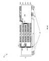
- FIG. 1Ais a diagram of a hybrid circuit comprising a transformer embedded in a multi-layer integrated circuit (IC) package, in accordance with an embodiment of the invention.
- a hybrid circuit 100(may also be referred to as a hybridized circuit, or a hybrid or hybridized package) comprising an IC 106 and a multi-layer IC package 104 .
- the IC 106may be flip chip bonded (also referred to as bump bonded) to the multi-layer IC package.
- the ICmay comprise a transceiver 423 and a signal strength indicator (SSI) 102 .
- the multi-layer IC package 104may comprise a transformer 112 and an antenna 421 .
- the antenna 421may be separate from the hybrid circuit 100 .
- a single transceiver 423is illustrated, the invention is not so limited. Accordingly, a separate transmitter and/or receiver may be utilized without departing from the scope of the invention.
- the IC 106may comprise suitable logic, circuitry, and/or code for performing one or more functions associated with transmitting and/or receiving RF signals.
- the IC 106may comprise all or a portion of the system 420 described with respect to FIG. 4 .
- the IC 106may utilize a transformer embedded in the multi-layer integrated circuit package 104 for transmitting and/or receiving RF signals.
- the transformer 112may enable coupling signals to be transmitted from the transceiver 423 to the antenna 421 and coupling signals received by the antenna 421 to the transceiver 423 .
- the windings ratio of the transformermay be configurable.
- the IC 106may comprise suitable logic, circuitry and/or code for configuring the transformer 112 .
- the SSI 102may comprise suitable logic, circuitry, and/or code that may enable determining signal strength.
- the SSI 102may, for example, be enabled to measure current, voltage, and/or power of the signal 101 . Additionally, the SSI 102 may be enabled to convey measurement results to other portions of the IC 106 .
- the SSI 102may output one or more digital and/or analog signals representative of the current, voltage, and/or power of the signal 101 .
- the one or more signals output by the SSI 102may be utilized by, for example, the processor 425 described with respect to FIG. 4 , to generate a control signal 103 .
- the multi-layer IC package 104may comprise one or more layers of metal and/or insulating material.
- the multi-layer IC package 104may be fabricated in a manner similar to or the same as the IC 106 .
- circuit elementssuch as resistors, inductors, capacitors, transmission lines, switches, and antennas, may be fabricated in one or more metal layers of the multi-layer package 104 .
- one or more switching elements and one or more transformersmay be fabricated in the multi-layer IC package 104 .
- a configurable transformer 112may be realized wherein opening/closing the switches may alter the windings ratio of the transformer 112 .
- one or more switching elements which may control the windings ratio of the transformermay be fabricated in the IC 106 .
- the transformer 112may comprise two or more windings and a core.
- the number of loops in the primary and/or secondary windingmay be configurable.
- the transformer 112may enable adjusting an impedance seen by signals communicatively coupled to the transformer 112 .
- voltage swings at an amplifier input and/or an amplifier outputmay be maintained within determined limits.
- the core of the transformer 112may comprise ferromagnetic material.
- the transceivermay comprise a power amplifier (PA) 108 which may output the signal 101 to the antenna 421 via the transformer 112 .
- PApower amplifier
- altering the windings ratio of the transformer 112may enable maintaining voltage and/or current levels of the signal 101 within determined limits. In this manner, damage to circuitry in the IC 106 and/or the multi-layer package 104 resulting from large voltage swings of the signal 101 may be prevented.
- the transceiver 423may comprise a low noise amplifier (LNA) 110 which may receive the signal 101 from the antenna 421 via the transformer 112 .
- LNAlow noise amplifier
- altering the windings ratio of the transformer 112may enable maintaining voltage and/or current levels of the signal 101 within determined limits. In this manner, damage to circuitry in the IC 106 , such as the LNA 110 , and/or in the multi-layer package 104 resulting from large voltage swings of the signal 101 may be prevented.
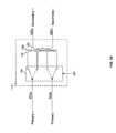
- FIG. 1Bis a diagram of a transformer with configurable windings ratio, in accordance with an embodiment of the invention. Referring to FIG. 1B there is shown a transformer 112 with terminals 152 a , 152 b , 162 a , and 162 b , a switch network 154 , a first winding 156 , a transformer core 158 , and a second winding 160 .
- the terminals 152 a and 152 bmay be inputs and/or outputs to the first winding 156 .
- the number of turns (also referred to as loops) between terminals 152 a and 152 bmay be variable.
- the terminals 162 a and 162 bmay be the inputs and/or outputs to the second winding 160 .
- the number of turns (loops) between the terminals 162 a and 162 bmay be fixed.
- the switch network 154may comprise suitable logic, circuitry, and/or code for communicatively coupling the terminals 152 a and 152 b to one or more turns of the first winding 156 .
- the switch network 154may be controlled via one or more control signals from, for example, the processor 425 and/or the baseband processor 427 described with respect to FIG. 4 .
- the switches, within the switch network 154in the position indicated by the solid lines may result in three turns between the terminals 152 a and 152 b , whereas the switches in the position indicated by the dashed lines may result in one turn between the terminals 152 a and 152 b .
- the winding 160has two turns.
- the windings ratiois configurable between 3:2 and 1:2 (first winding: second winding).
- the transformer core 518may comprise a material suitable for concentrating the flux generated by one winding to induce a current in the other winding.
- the coremay comprise ferromagnetic material within the multi-layer IC package 104 .
- the first winding 156may be the primary winding or the secondary winding
- the second winding 160may be the secondary winding or the primary winding.
- both windingsmay comprise a variable number of turns configured via one or more switch networks.
- the control signalmay configure the switch network 154 based on, for example, voltage and/or current levels at the terminals 152 a , 152 b and terminals 162 a , 162 b .
- the terminal 152 a , 152 bmay be communicatively coupled to a power amplifier and the terminals 162 a , 162 b may be coupled to an antenna.
- the switchesmay be in the dashed line configuration for high output power and the switches may be in the solid line configuration for low PA output power. In this manner, the voltage swing at the output of the PA may be maintained, for example, within safe levels so as not to damage CMOS circuitry.
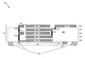
- FIG. 2Ais a diagram illustrating a cross sectional view of a multi-layer package with embedded transformer, in accordance with an embodiment of the invention.
- a hybrid circuit 100comprising an IC 106 and a multi-layer IC package 104 .
- the multi-layer IC package 104may comprise an insulating material 203 ; metal layers 202 ; vias 220 a , 220 b (not shown), 222 a , 222 b (not shown), 224 , and 226 ; and MEMS switches 154 .
- the multi-layer IC package 104may comprise one or more layers and/or areas of ferromagnetic and/or ferrimagnetic material.
- the IC 106may be coupled to the multi-layer IC package 104 , and the package 104 to a PCB (not shown), via solder balls 208 .
- Surface mount component(s) 252may be mounted to the multi-layer IC package 104 , and thermal epoxy 214 may be pressed between the IC 106 and the multi-layer IC package 104 .
- the IC 106may be as described with respect to FIG. 1 . Additionally, the IC 106 may be flip-chip bonded (also referred to as bump bonded) to the multi-layer IC package 104 utilizing solder balls (e.g. solder balls 208 as described with respect to FIG. 2A below). In this manner, wire bonds connecting the IC 106 to the multi-layer IC package 104 may be eliminated, reducing and/or eliminating stray inductances due to wire bonds. In addition, the thermal conductance out of the IC 106 may be greatly improved utilizing the solder balls 208 and the thermal epoxy 214 .
- the thermal epoxy 214may be electrically insulating but thermally conductive to allow for thermal energy to be conducted out of the IC 106 to the much larger thermal mass of the multilayer package 104 .
- the solder balls 208may comprise spherical balls of metal to provide electrical, thermal and physical contact between the IC 106 and the multi-layer IC package 104 .
- the IC 106may be pressed with enough force to squash the metal spheres somewhat, and may be performed at an elevated temperature to provide suitable electrical resistance and physical bond strength.
- the solder balls 208may also be utilized to provide electrical, thermal and physical contact between the multi-layer IC package 104 and a printed circuit board comprising other parts of, for example, the wireless system 420 described with respect to FIG. 4 .
- the surface mount device(s) 252may comprise discrete circuit element(s) such as resistors, capacitors, inductors, and diodes, for example.
- the surface mount device(s) 252may be soldered to the multi-layer IC package 104 to provide electrical contact.
- additional surface mount elements or no surface mount elementsmay be coupled to the multi-layer IC package 104 .
- the metal layer 202may each comprise a deposited metal layer utilized to delineate the two transformer windings 156 (comprised of loops 156 1 , 156 2 , and 156 3 ) and 160 (comprised of loops 160 1 , 160 2 ) described with respect to FIG. 1B and the antenna 421 described with respect to FIG. 4 .
- the metal layer 202may be deposited in shapes and/or sizes which may enable varying characteristics of the transformer 112 and the antenna 421 .
- the vias 220 a , 220 b (not shown), 222 a , 222 b (not shown)may comprise metal and/or other conductive material(s) which may communicatively couple the metal layers 202 to one another and to the solder balls 208 . In this manner, signals may be conveyed to and/or from the transformer windings 156 and 160 , the IC 106 , and the antenna 421 .
- vias 220 a 222 amay communicatively couple positive terminals of loops 156 1 , 156 2 , and 156 3 and vias 220 b and 222 b (not shown) may couple negative terminals of loops 156 1 , 156 2 , and 156 3 .
- via 224may connect a negative terminal of loop 160 1 to a positive terminal of loop 160 2 .
- additional and/or alternative viasmay communicatively couple the transformer loops to each other and/or to the IC 106 .
- the switch network 154 described with respect to FIG. 1Bmay be implemented as MEMS switches in the multi-layer IC package 104 .
- the MEMS switches 154may close when, for example a magnetic field is induced on a switch terminal.
- the MEMS switches 154may each comprise a thin conductive element or film which in the open position is suspended above a switch terminal (as indicated by the solid lines in FIG. 2 ) and in the closed position is in contact with a switch terminal (as indicated by the dashed lines in FIG. 2 ). Accordingly, energizing the terminal, for example, may generate an attracting force that draws the element of film into contact with the terminal.
- the transformermay be configured via one or more switches integrated on the IC 106 .
- the IC 106 and associated multi-layer IC package 104may be utilized to transmit and/or receive RF signals.
- the IC 106may be electrically coupled to the antenna 421 embedded on and/or within the multi-layer IC package 104 via a configurable transformer embedded on and/or within the multi-layer IC package 104 .
- the windings ratio of the transformermay be configured via the switch network 154 . In this regard, when both switches are closed the windings ratio may be 3:2, when one switch is open the windings ratio may be 2:2, and when both switches are open the windings ratio may be 1:2.
- Logic, circuitry, and/or code in the IC 106may control the switches 154 .
- additional devicese.g., capacitors, inductors, resistors
- capacitors, inductors, resistorsmay be integrated into the multi-layer IC package without deviating from the scope of the present invention.
- additional devicese.g., capacitors, inductors, resistors
- transformerscomprising five loops
- various exemplary embodiments of the inventionmay comprise any number of metal layers, transformer loops, and/or switching elements without deviating from the scope of the invention.
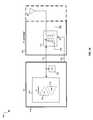
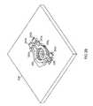
- FIG. 2Bis an exemplary top view of a transformer embedded in a multi-layer IC package, in accordance with an embodiment of the invention.
- a multi-layer IC package 104with embedded transformer.
- FIG. 2Bmay be an alternate view of the transformer 112 described with respect to FIGS. 1A , 1 B and 2 A. Shown in FIG. 2B , but not depicted in FIG. 2A , are the terminal 250 and the capacitors 252 a , 252 b , and 252 c.
- the terminal 250may provide a tap into the winding 156 such that a DC bias may be applied to the winding.
- a DC bias applied to the center of the winding 156may be utilized, for example, when a balanced (differential) signal is communicatively coupled to the winding 156 .
- the capacitors 252 a , 252 b , 252 cmay be bypass capacitors to ground, which may be communicatively coupled to the terminals 152 a and 152 b of the winding 156 and communicatively coupled to the positive terminal 226 of the winding 160 .
- the antenna 421 of FIG. 2Ais not shown in FIG. 2B .
- FIG. 3is a flow chart illustrating exemplary steps for configuring a transformer embedded in a multi-layer IC package, in accordance with an embodiment of the invention.
- the exemplary stepsmay advance to step 304 .
- signal levels at the transformermay be measured.
- an output of a power amplifiersuch as the PA 108 described with respect to FIG. 1A
- a primary windingmay be coupled to an antenna such as the antenna 421 described with respect to FIG.
- a secondary windingmay be coupled to a low noise amplifier, such as the LNA 110 described with respect to FIG. 1A . Accordingly, voltage across the secondary winding may be measured. Measurements performed in step 304 may be performed by a SSI such as the SSI 102 described with respect to FIG. 1A . Additionally, measurement results may be conveyed to, for example, a memory and/or a processor, such that one or more control signals may be generated for configuring the transformer. Subsequent to step 304 , the exemplary steps may advance to step 306 . In step 306 , the windings ratio of the transformer may be adjusted such that the measured voltage levels are within determined limits.
- step 306the exemplary steps may advance to step 308 .
- step 308signals may be received from and/or transmitted to an antenna via the configured transformer.
- FIG. 4is a block diagram illustrating an exemplary wireless device, in accordance with an embodiment of the invention.
- a wireless device 420may comprise an RF transceiver 423 , a digital baseband processor 429 , a processor 425 , and a memory 427 .
- the transceiver 423may comprise a receiver 423 b and a transmitter 423 a .
- An antenna 421may be communicatively coupled to the RF transceiver 423 via the transformer 112 .
- the wireless device 420may be operated in a system, such as the cellular network and/or digital video broadcast network, for example.
- the antenna 421may comprise one or more antenna elements which may be coupled and/or decoupled via one or more switching elements.
- the antenna 421may be configured based on factors comprising frequency, polarization, and/or gain.
- the antenna 421may be a phased array antenna. In this regard, the directivity of the antenna may be controlled by adjusting the phase(s) of signals communicatively coupled to the antenna.
- the RF receiver 423 bmay comprise suitable logic, circuitry, and/or code that may enable processing of received RF signals.
- the RF receiver 423 bmay enable receiving RF signals in a plurality of frequency bands.
- the RF receiver 423 bmay enable receiving signals in extremely high frequency (e.g., 60 GHz) bands.
- the receiver 423 bmay be enabled to receive, filter, amplify, down-convert, and/or perform analog to digital conversion.
- the RF receiver 423 bmay down convert a received RF signal.
- the RF receiver 423 bmay perform direct down conversion of the received RF signal to a baseband or may convert the received RF signal to an intermediate frequency (IF).
- IFintermediate frequency
- the receiver 423 bmay perform quadrature down-conversion where in-phase components and quadrature phase components may be processed in parallel.
- the receiver 423 bmay be enabled to receive signals via the transformer 112 , which may be configurable and provide a means of controlling signal levels at its primary and/or secondary windings.
- the wireless device 420may comprise a plurality of the receivers 423 b and may thus support multiple frequency bands and or simultaneous reception of signals in the same frequency band.
- the digital baseband processor 429may comprise suitable logic, circuitry, and/or code that may enable processing and/or handling of baseband signals.
- the digital baseband processor 429may process or handle signals received from the RF receiver 423 b and/or signals to be transferred to the RF transmitter 423 a , when the RF transmitter 423 a is present, for transmission to the network.
- the digital baseband processor 429may also provide control and/or feedback information to the RF receiver 423 b and to the RF transmitter 423 a based on information from the processed signals.
- the baseband processor 429may provide one or more control signals for configuring the transformer 112 via one or more switching elements.
- the digital baseband processor 429may communicate information and/or data from the processed signals to the processor 425 and/or to the memory 427 . Moreover, the digital baseband processor 429 may receive information from the processor 425 and/or to the memory 427 , which may be processed and transferred to the RF transmitter 423 a for transmission to the network.
- the RF transmitter 423 amay comprise suitable logic, circuitry, and/or code that may enable processing of RF signals for transmission.
- the transmitter 423 amay be enabled to transmit signals via the transformer 112 , which may be configurable and provide a means of controlling signal levels at its primary and/or secondary windings.
- the RF transmitter 423 amay enable transmission of RF signals in a plurality of frequency bands.
- the RF transmitter 423 amay enable transmitting signals in cellular frequency bands.
- Each frequency band supported by the RF transmitter 423 amay have a corresponding front-end circuit for handling amplification and up conversion operations, for example.
- the RF transmitter 423 amay be referred to as a multi-band transmitter when it supports more than one frequency band.
- the wireless device 420may comprise more than one RF transmitter 423 a , wherein each of the RF transmitter 423 a may be a single-band or a multi-band transmitter.
- the RF transmitter 423 amay perform direct up conversion of the baseband signal to an RF signal. In some instances, the RF transmitter 423 a may enable digital-to-analog conversion of the baseband signal components received from the digital baseband processor 429 before up conversion. In other instances, the RF transmitter 423 a may receive baseband signal components in analog form.
- the processor 425may comprise suitable logic, circuitry, and/or code that may enable control and/or data processing operations for the wireless device 420 .
- the processor 425may be utilized to control at least a portion of the RF receiver 423 b , the RF transmitter 423 a , the digital baseband processor 429 , and/or the memory 427 .
- the processor 425may generate at least one signal for controlling operations within the wireless device 420 .
- the baseband processor 429may provide one or more control signals for configuring the transformer 112 via one or more switching elements.
- the processor 425may also enable executing of applications that may be utilized by the wireless device 420 .
- the processor 425may execute applications that may enable displaying and/or interacting with content received via cellular transmission signals in the wireless device 420 .
- the memory 427may comprise suitable logic, circuitry, and/or code that may enable storage of data and/or other information utilized by the wireless device 420 .
- the memory 427may be utilized for storing processed data generated by the digital baseband processor 429 and/or the processor 425 .
- the memory 427may also be utilized to store information, such as configuration information, that may be utilized to control the operation of at least one block in the wireless device 420 .
- the memory 427may comprise information necessary to configure the transformer 112 .
- the memorymay store control and/or configuration information for configuring the windings ratio of the transformer 112 via one or more switching elements.
- a windings ratio of a transformer, such as the transformer 112 , embedded in a multi-layer IC package, such as the IC package 104may be configured; via logic, circuitry, and/or code in an IC, such as the IC 106 ; based on signal levels at one or more terminals of the transformer.
- the transformer 112may comprise a plurality of inductive loops fabricated in a plurality of metal layers, such as the loops 156 and 160 described with respect to FIG. 2A , of the IC package 104 .
- the loops 156 and/or 160may be fabricated in transmission line media such as microstrip and/or stripline.
- the IC 106may be flip-chip bonded to the IC package and may comprise one or more amplifiers, such as the PA 108 and the LNA 110 , communicatively coupled to the transformer 112 and/or a signal strength indicator, such as the SSI 102 , enabled to measure signal levels input to or output by the transformer.
- the windings ratiomay be configured via one or more switches, such as the switching element 154 , which may comprise active devices in the IC 106 and/or MEMS switches in the multi-layer package 104 .
- the IC 106 and/or the multi-layer package 104may comprise ferromagnetic material which may improve magnetic coupling of the transformer.
- Another embodiment of the inventionmay provide a machine-readable storage, having stored thereon, a computer program having at least one code section executable by a machine, thereby causing the machine to perform the steps as described herein for configuring a transformer embedded in a multi-layer IC package.
- the present inventionmay be realized in hardware, software, or a combination of hardware and software.
- the present inventionmay be realized in a centralized fashion in at least one computer system, or in a distributed fashion where different elements are spread across several interconnected computer systems. Any kind of computer system or other apparatus adapted for carrying out the methods described herein is suited.
- a typical combination of hardware and softwaremay be a general-purpose computer system with a computer program that, when being loaded and executed, controls the computer system such that it carries out the methods described herein.
- the present inventionmay also be embedded in a computer program product, which comprises all the features enabling the implementation of the methods described herein, and which when loaded in a computer system is able to carry out these methods.
- Computer program in the present contextmeans any expression, in any language, code or notation, of a set of instructions intended to cause a system having an information processing capability to perform a particular function either directly or after either or both of the following: a) conversion to another language, code or notation; b) reproduction in a different material form.
Landscapes
- Engineering & Computer Science (AREA)
- Power Engineering (AREA)
- Computer Networks & Wireless Communication (AREA)
- Signal Processing (AREA)
- Microelectronics & Electronic Packaging (AREA)
- Quality & Reliability (AREA)
- Physics & Mathematics (AREA)
- Electromagnetism (AREA)
- Semiconductor Integrated Circuits (AREA)
- Coils Or Transformers For Communication (AREA)
Abstract
Description
Claims (20)
Priority Applications (2)
| Application Number | Priority Date | Filing Date | Title |
|---|---|---|---|
| US12/057,714US8198714B2 (en) | 2008-03-28 | 2008-03-28 | Method and system for configuring a transformer embedded in a multi-layer integrated circuit (IC) package |
| US13/491,421US8912639B2 (en) | 2008-03-28 | 2012-06-07 | IC package with embedded transformer |
Applications Claiming Priority (1)
| Application Number | Priority Date | Filing Date | Title |
|---|---|---|---|
| US12/057,714US8198714B2 (en) | 2008-03-28 | 2008-03-28 | Method and system for configuring a transformer embedded in a multi-layer integrated circuit (IC) package |
Related Child Applications (1)
| Application Number | Title | Priority Date | Filing Date |
|---|---|---|---|
| US13/491,421ContinuationUS8912639B2 (en) | 2008-03-28 | 2012-06-07 | IC package with embedded transformer |
Publications (2)
| Publication Number | Publication Date |
|---|---|
| US20090243767A1 US20090243767A1 (en) | 2009-10-01 |
| US8198714B2true US8198714B2 (en) | 2012-06-12 |
Family
ID=41116231
Family Applications (2)
| Application Number | Title | Priority Date | Filing Date |
|---|---|---|---|
| US12/057,714Expired - Fee RelatedUS8198714B2 (en) | 2008-03-28 | 2008-03-28 | Method and system for configuring a transformer embedded in a multi-layer integrated circuit (IC) package |
| US13/491,421Active2028-07-06US8912639B2 (en) | 2008-03-28 | 2012-06-07 | IC package with embedded transformer |
Family Applications After (1)
| Application Number | Title | Priority Date | Filing Date |
|---|---|---|---|
| US13/491,421Active2028-07-06US8912639B2 (en) | 2008-03-28 | 2012-06-07 | IC package with embedded transformer |
Country Status (1)
| Country | Link |
|---|---|
| US (2) | US8198714B2 (en) |
Cited By (3)
| Publication number | Priority date | Publication date | Assignee | Title |
|---|---|---|---|---|
| US20170271260A1 (en)* | 2016-03-18 | 2017-09-21 | Infineon Technologies Ag | Semiconductor device including a passive component formed in a redistribution layer |
| US20230239008A1 (en)* | 2022-01-26 | 2023-07-27 | Pixart Imaging Inc. | Inductor circuit and wireless communication device having inductor circuit integrated on single chip die to save more circuit costs |
| US20230370120A1 (en)* | 2022-01-26 | 2023-11-16 | Pixart Imaging Inc. | Inductor circuit and wireless communication device having inductor circuit integrated on single chip die to save more circuit costs |
Families Citing this family (14)
| Publication number | Priority date | Publication date | Assignee | Title |
|---|---|---|---|---|
| US7880677B2 (en)* | 2007-12-12 | 2011-02-01 | Broadcom Corporation | Method and system for a phased array antenna embedded in an integrated circuit package |
| US20090153260A1 (en)* | 2007-12-12 | 2009-06-18 | Ahmadreza Rofougaran | Method and system for a configurable transformer integrated on chip |
| US8270912B2 (en)* | 2007-12-12 | 2012-09-18 | Broadcom Corporation | Method and system for a transformer in an integrated circuit package |
| US8144674B2 (en)* | 2008-03-27 | 2012-03-27 | Broadcom Corporation | Method and system for inter-PCB communications with wireline control |
| US7911388B2 (en)* | 2007-12-12 | 2011-03-22 | Broadcom Corporation | Method and system for configurable antenna in an integrated circuit package |
| US8855093B2 (en)* | 2007-12-12 | 2014-10-07 | Broadcom Corporation | Method and system for chip-to-chip communications with wireline control |
| US8583197B2 (en)* | 2007-12-12 | 2013-11-12 | Broadcom Corporation | Method and system for sharing antennas for high frequency and low frequency applications |
| US8494030B2 (en)* | 2008-06-19 | 2013-07-23 | Broadcom Corporation | Method and system for 60 GHz wireless clock distribution |
| US8106829B2 (en) | 2007-12-12 | 2012-01-31 | Broadcom Corporation | Method and system for an integrated antenna and antenna management |
| US8086190B2 (en)* | 2008-03-27 | 2011-12-27 | Broadcom Corporation | Method and system for reconfigurable devices for multi-frequency coexistence |
| US8116676B2 (en)* | 2008-05-07 | 2012-02-14 | Broadcom Corporation | Method and system for inter IC communications utilizing a spatial multi-link repeater |
| US8660500B2 (en) | 2009-06-09 | 2014-02-25 | Broadcom Corporation | Method and system for a voltage-controlled oscillator with a leaky wave antenna |
| US8588686B2 (en)* | 2009-06-09 | 2013-11-19 | Broadcom Corporation | Method and system for remote power distribution and networking for passive devices |
| US11387558B2 (en)* | 2019-12-20 | 2022-07-12 | Rockwell Collins, Inc. | Loop antenna polarization control |
Citations (48)
| Publication number | Priority date | Publication date | Assignee | Title |
|---|---|---|---|---|
| US3532986A (en)* | 1968-03-18 | 1970-10-06 | Warren G Gelushia | Electric warning system for vehicles |
| US4785345A (en)* | 1986-05-08 | 1988-11-15 | American Telephone And Telegraph Co., At&T Bell Labs. | Integrated transformer structure with primary winding in substrate |
| JPH0319358A (en) | 1989-06-16 | 1991-01-28 | Matsushita Electron Corp | Semiconductor integrated circuit |
| US5003622A (en) | 1989-09-26 | 1991-03-26 | Astec International Limited | Printed circuit transformer |
| US5015972A (en) | 1989-08-17 | 1991-05-14 | Motorola, Inc. | Broadband RF transformer |
| US5619121A (en)* | 1995-06-29 | 1997-04-08 | Siemens Energy & Automation, Inc. | Load voltage based tap changer monitoring system |
| US5798567A (en) | 1997-08-21 | 1998-08-25 | Hewlett-Packard Company | Ball grid array integrated circuit package which employs a flip chip integrated circuit and decoupling capacitors |
| US5861853A (en) | 1997-05-07 | 1999-01-19 | Motorola, Inc. | Current balanced balun network with selectable port impedances |
| US5914873A (en)* | 1997-06-30 | 1999-06-22 | Advanced Micro Devices | Distributed voltage converter apparatus and method for high power microprocessor with array connections |
| US20020039026A1 (en)* | 2000-04-04 | 2002-04-04 | Stroth John E. | Power line testing device with signal generator and signal detector |
| US20020047601A1 (en)* | 1998-12-11 | 2002-04-25 | Shannon John Robert | Method and apparatus for controlling a discharge lamp in a backlighted display |
| US6462976B1 (en)* | 1997-02-21 | 2002-10-08 | University Of Arkansas | Conversion of electrical energy from one form to another, and its management through multichip module structures |
| US20030142513A1 (en)* | 2002-01-31 | 2003-07-31 | Patrizio Vinciarelli | Factorized power architecture with point of load sine amplitude converters |
| US20040075499A1 (en)* | 2000-09-12 | 2004-04-22 | Dupuis Timothy J. | PF power detector |
| US20040095277A1 (en)* | 2002-11-19 | 2004-05-20 | Farrokh Mohamadi | Inductively-coupled antenna array |
| US20040101312A1 (en)* | 2002-08-29 | 2004-05-27 | Florencio Cabrera | AC power source light modulation network |
| US20040150554A1 (en) | 2003-02-05 | 2004-08-05 | Stenger Peter A. | Low profile active electronically scanned antenna (AESA) for Ka-band radar systems |
| US6801114B2 (en) | 2002-01-23 | 2004-10-05 | Broadcom Corp. | Integrated radio having on-chip transformer balun |
| US20040201526A1 (en) | 2003-04-11 | 2004-10-14 | Gareth Knowles | Matrix architecture switch controlled adjustable performance electromagnetic energy coupling mechanisms using digital controlled single source supply |
| US6809581B2 (en) | 2002-04-23 | 2004-10-26 | Broadcom Corp. | Integrated circuit low noise amplifier and applications thereof |
| US20040222506A1 (en) | 2002-10-15 | 2004-11-11 | Silicon Laboratories, Inc. | Integrated circuit package configuration incorporating shielded circuit element structure |
| US6848178B2 (en)* | 2002-05-30 | 2005-02-01 | Denso Corporation | Enhancement of current-carrying capacity of a multilayer circuit board |
| US20050212642A1 (en)* | 2004-03-26 | 2005-09-29 | Harris Corporation | Embedded toroidal transformers in ceramic substrates |
| US20050270135A1 (en)* | 2000-05-17 | 2005-12-08 | Xerox Corporation | Method of making photolithographically-patterned out-of-plane coil structures |
| US20060091958A1 (en)* | 2004-10-28 | 2006-05-04 | Broadcom Corporation | Multilevel power amplifier architecture using multi-tap transformer |
| US7054279B2 (en)* | 2000-04-07 | 2006-05-30 | Broadcom Corporation | Method and apparatus for optimizing signal transformation in a frame-based communications network |
| US20060152911A1 (en)* | 2005-01-10 | 2006-07-13 | Ixys Corporation | Integrated packaged having magnetic components |
| US7081800B2 (en) | 2004-06-30 | 2006-07-25 | Intel Corporation | Package integrated one-quarter wavelength and three-quarter wavelength balun |
| US20060244527A1 (en)* | 2003-10-17 | 2006-11-02 | Sanken Electric Co., Ltd. | Amplifying circuit, noise reducing apparatus and power converting apparatus |
| US20060267717A1 (en) | 2005-05-24 | 2006-11-30 | Posamentier Joshua D | Multi-tap microelectromechanical inductor |
| US20070139112A1 (en)* | 2000-09-12 | 2007-06-21 | Bocock Ryan M | Method and apparatus for stabilizing rf power amplifiers |
| US7247932B1 (en) | 2000-05-19 | 2007-07-24 | Megica Corporation | Chip package with capacitor |
| US20070205748A1 (en)* | 2006-03-01 | 2007-09-06 | Toyota Jidosha Kabushiki Kaisha | Signal transmission device |
| US20080048760A1 (en) | 2006-07-29 | 2008-02-28 | Samir El Rai | Monolithically integratable circuit arrangement |
| US20080049373A1 (en)* | 2006-07-19 | 2008-02-28 | Sharp Kabushiki Kaisha | High voltage output device and ion generator provided therewith |
| US7427977B2 (en)* | 2003-12-16 | 2008-09-23 | Lg Display Co., Ltd. | Lamp driving device for liquid crystal display device |
| US20080291115A1 (en) | 2007-05-22 | 2008-11-27 | Sibeam, Inc. | Surface mountable integrated circuit packaging scheme |
| US20090046489A1 (en)* | 2007-04-19 | 2009-02-19 | Fuji Electric Device Technology Co., Ltd | Insulated transformers, and power converting device |
| US20090153421A1 (en) | 2007-12-12 | 2009-06-18 | Ahmadreza Rofougaran | Method and system for an integrated antenna and antenna management |
| US20090153427A1 (en) | 2007-12-12 | 2009-06-18 | Ahmadreza Rofougaran | Method and system for configurable antenna in an integrated circuit package |
| US20090153260A1 (en) | 2007-12-12 | 2009-06-18 | Ahmadreza Rofougaran | Method and system for a configurable transformer integrated on chip |
| US20090156157A1 (en) | 2007-12-12 | 2009-06-18 | Ahmadreza Rofougaran | Method and system for a transformer in an integrated circuit package |
| US20090189064A1 (en)* | 2005-07-26 | 2009-07-30 | Sionex Corporation | Ultra compact ion mobility based analyzer apparatus, method, and system |
| US20090243741A1 (en) | 2008-03-27 | 2009-10-01 | Ahmadreza Rofougaran | Method and system for processing signals via an oscillator load embedded in an integrated circuit (ic) package |
| US20090243749A1 (en) | 2008-03-27 | 2009-10-01 | Ahmadreza Rofougaran | Method and system for configurable differential or single-ended signaling in an integrated circuit |
| US20090243535A1 (en)* | 2008-03-31 | 2009-10-01 | Johnson Controls Technology Company | Multi-Input Relay Board |
| US20100052839A1 (en)* | 2008-09-04 | 2010-03-04 | Koen Mertens | Transformers and Methods of Manufacture Thereof |
| US7880677B2 (en) | 2007-12-12 | 2011-02-01 | Broadcom Corporation | Method and system for a phased array antenna embedded in an integrated circuit package |
Family Cites Families (6)
| Publication number | Priority date | Publication date | Assignee | Title |
|---|---|---|---|---|
| US3740488A (en)* | 1971-01-13 | 1973-06-19 | Westinghouse Electric Corp | Inductive loop through-the-earth communication system |
| US5525941A (en)* | 1993-04-01 | 1996-06-11 | General Electric Company | Magnetic and electromagnetic circuit components having embedded magnetic material in a high density interconnect structure |
| US6927663B2 (en)* | 2003-07-23 | 2005-08-09 | Cardiac Pacemakers, Inc. | Flyback transformer wire attach method to printed circuit board |
| DE102004011203B4 (en)* | 2004-03-04 | 2010-09-16 | Robert Bosch Gmbh | Method for mounting semiconductor chips and corresponding semiconductor chip arrangement |
| US7280024B2 (en)* | 2005-02-02 | 2007-10-09 | Intel Corporation | Integrated transformer structure and method of fabrication |
| DE102006057332B4 (en)* | 2006-12-05 | 2018-01-25 | Infineon Technologies Ag | Assembly comprising a substrate and a chip mounted on the substrate |
- 2008
- 2008-03-28USUS12/057,714patent/US8198714B2/ennot_activeExpired - Fee Related
- 2012
- 2012-06-07USUS13/491,421patent/US8912639B2/enactiveActive
Patent Citations (51)
| Publication number | Priority date | Publication date | Assignee | Title |
|---|---|---|---|---|
| US3532986A (en)* | 1968-03-18 | 1970-10-06 | Warren G Gelushia | Electric warning system for vehicles |
| US4785345A (en)* | 1986-05-08 | 1988-11-15 | American Telephone And Telegraph Co., At&T Bell Labs. | Integrated transformer structure with primary winding in substrate |
| JPH0319358A (en) | 1989-06-16 | 1991-01-28 | Matsushita Electron Corp | Semiconductor integrated circuit |
| US5015972A (en) | 1989-08-17 | 1991-05-14 | Motorola, Inc. | Broadband RF transformer |
| US5003622A (en) | 1989-09-26 | 1991-03-26 | Astec International Limited | Printed circuit transformer |
| US5619121A (en)* | 1995-06-29 | 1997-04-08 | Siemens Energy & Automation, Inc. | Load voltage based tap changer monitoring system |
| US6462976B1 (en)* | 1997-02-21 | 2002-10-08 | University Of Arkansas | Conversion of electrical energy from one form to another, and its management through multichip module structures |
| US5861853A (en) | 1997-05-07 | 1999-01-19 | Motorola, Inc. | Current balanced balun network with selectable port impedances |
| US5914873A (en)* | 1997-06-30 | 1999-06-22 | Advanced Micro Devices | Distributed voltage converter apparatus and method for high power microprocessor with array connections |
| US5798567A (en) | 1997-08-21 | 1998-08-25 | Hewlett-Packard Company | Ball grid array integrated circuit package which employs a flip chip integrated circuit and decoupling capacitors |
| US20020047601A1 (en)* | 1998-12-11 | 2002-04-25 | Shannon John Robert | Method and apparatus for controlling a discharge lamp in a backlighted display |
| US20030161164A1 (en)* | 1998-12-11 | 2003-08-28 | Monolithic Power Systems, Inc. | Method and apparatus for controlling a discharge lamp in a backlighted display |
| US20020039026A1 (en)* | 2000-04-04 | 2002-04-04 | Stroth John E. | Power line testing device with signal generator and signal detector |
| US7054279B2 (en)* | 2000-04-07 | 2006-05-30 | Broadcom Corporation | Method and apparatus for optimizing signal transformation in a frame-based communications network |
| US20050270135A1 (en)* | 2000-05-17 | 2005-12-08 | Xerox Corporation | Method of making photolithographically-patterned out-of-plane coil structures |
| US7247932B1 (en) | 2000-05-19 | 2007-07-24 | Megica Corporation | Chip package with capacitor |
| US20040075499A1 (en)* | 2000-09-12 | 2004-04-22 | Dupuis Timothy J. | PF power detector |
| US20080284512A1 (en)* | 2000-09-12 | 2008-11-20 | Susanne A Paul | Power amplifier circuitry and method |
| US20070139112A1 (en)* | 2000-09-12 | 2007-06-21 | Bocock Ryan M | Method and apparatus for stabilizing rf power amplifiers |
| US6801114B2 (en) | 2002-01-23 | 2004-10-05 | Broadcom Corp. | Integrated radio having on-chip transformer balun |
| US20040207504A1 (en) | 2002-01-23 | 2004-10-21 | Yang Hung Yu | On-chip transformer balun |
| US20030142513A1 (en)* | 2002-01-31 | 2003-07-31 | Patrizio Vinciarelli | Factorized power architecture with point of load sine amplitude converters |
| US6809581B2 (en) | 2002-04-23 | 2004-10-26 | Broadcom Corp. | Integrated circuit low noise amplifier and applications thereof |
| US6848178B2 (en)* | 2002-05-30 | 2005-02-01 | Denso Corporation | Enhancement of current-carrying capacity of a multilayer circuit board |
| US20040101312A1 (en)* | 2002-08-29 | 2004-05-27 | Florencio Cabrera | AC power source light modulation network |
| US20040222506A1 (en) | 2002-10-15 | 2004-11-11 | Silicon Laboratories, Inc. | Integrated circuit package configuration incorporating shielded circuit element structure |
| US20040095277A1 (en)* | 2002-11-19 | 2004-05-20 | Farrokh Mohamadi | Inductively-coupled antenna array |
| US20040150554A1 (en) | 2003-02-05 | 2004-08-05 | Stenger Peter A. | Low profile active electronically scanned antenna (AESA) for Ka-band radar systems |
| US20040201526A1 (en) | 2003-04-11 | 2004-10-14 | Gareth Knowles | Matrix architecture switch controlled adjustable performance electromagnetic energy coupling mechanisms using digital controlled single source supply |
| US20060244527A1 (en)* | 2003-10-17 | 2006-11-02 | Sanken Electric Co., Ltd. | Amplifying circuit, noise reducing apparatus and power converting apparatus |
| US7427977B2 (en)* | 2003-12-16 | 2008-09-23 | Lg Display Co., Ltd. | Lamp driving device for liquid crystal display device |
| US20050212642A1 (en)* | 2004-03-26 | 2005-09-29 | Harris Corporation | Embedded toroidal transformers in ceramic substrates |
| US7081800B2 (en) | 2004-06-30 | 2006-07-25 | Intel Corporation | Package integrated one-quarter wavelength and three-quarter wavelength balun |
| US20060091958A1 (en)* | 2004-10-28 | 2006-05-04 | Broadcom Corporation | Multilevel power amplifier architecture using multi-tap transformer |
| US20060152911A1 (en)* | 2005-01-10 | 2006-07-13 | Ixys Corporation | Integrated packaged having magnetic components |
| US20060267717A1 (en) | 2005-05-24 | 2006-11-30 | Posamentier Joshua D | Multi-tap microelectromechanical inductor |
| US20090189064A1 (en)* | 2005-07-26 | 2009-07-30 | Sionex Corporation | Ultra compact ion mobility based analyzer apparatus, method, and system |
| US20070205748A1 (en)* | 2006-03-01 | 2007-09-06 | Toyota Jidosha Kabushiki Kaisha | Signal transmission device |
| US20080049373A1 (en)* | 2006-07-19 | 2008-02-28 | Sharp Kabushiki Kaisha | High voltage output device and ion generator provided therewith |
| US20080048760A1 (en) | 2006-07-29 | 2008-02-28 | Samir El Rai | Monolithically integratable circuit arrangement |
| US20090046489A1 (en)* | 2007-04-19 | 2009-02-19 | Fuji Electric Device Technology Co., Ltd | Insulated transformers, and power converting device |
| US20080291115A1 (en) | 2007-05-22 | 2008-11-27 | Sibeam, Inc. | Surface mountable integrated circuit packaging scheme |
| US20090153421A1 (en) | 2007-12-12 | 2009-06-18 | Ahmadreza Rofougaran | Method and system for an integrated antenna and antenna management |
| US20090153427A1 (en) | 2007-12-12 | 2009-06-18 | Ahmadreza Rofougaran | Method and system for configurable antenna in an integrated circuit package |
| US20090153260A1 (en) | 2007-12-12 | 2009-06-18 | Ahmadreza Rofougaran | Method and system for a configurable transformer integrated on chip |
| US20090156157A1 (en) | 2007-12-12 | 2009-06-18 | Ahmadreza Rofougaran | Method and system for a transformer in an integrated circuit package |
| US7880677B2 (en) | 2007-12-12 | 2011-02-01 | Broadcom Corporation | Method and system for a phased array antenna embedded in an integrated circuit package |
| US20090243741A1 (en) | 2008-03-27 | 2009-10-01 | Ahmadreza Rofougaran | Method and system for processing signals via an oscillator load embedded in an integrated circuit (ic) package |
| US20090243749A1 (en) | 2008-03-27 | 2009-10-01 | Ahmadreza Rofougaran | Method and system for configurable differential or single-ended signaling in an integrated circuit |
| US20090243535A1 (en)* | 2008-03-31 | 2009-10-01 | Johnson Controls Technology Company | Multi-Input Relay Board |
| US20100052839A1 (en)* | 2008-09-04 | 2010-03-04 | Koen Mertens | Transformers and Methods of Manufacture Thereof |
Non-Patent Citations (1)
| Title |
|---|
| Perndl, "Monolithic Microwave Integrated Circuits in SiGe:C Bipolar Technology" Dissertation, Nov. 2004. |
Cited By (5)
| Publication number | Priority date | Publication date | Assignee | Title |
|---|---|---|---|---|
| US20170271260A1 (en)* | 2016-03-18 | 2017-09-21 | Infineon Technologies Ag | Semiconductor device including a passive component formed in a redistribution layer |
| US10186481B2 (en)* | 2016-03-18 | 2019-01-22 | Infineon Technologies Ag | Semiconductor device including a passive component formed in a redistribution layer |
| US20230239008A1 (en)* | 2022-01-26 | 2023-07-27 | Pixart Imaging Inc. | Inductor circuit and wireless communication device having inductor circuit integrated on single chip die to save more circuit costs |
| US11750247B2 (en)* | 2022-01-26 | 2023-09-05 | Pixart Imaging Inc. | Inductor circuit and wireless communication device having inductor circuit integrated on single chip die to save more circuit costs |
| US20230370120A1 (en)* | 2022-01-26 | 2023-11-16 | Pixart Imaging Inc. | Inductor circuit and wireless communication device having inductor circuit integrated on single chip die to save more circuit costs |
Also Published As
| Publication number | Publication date |
|---|---|
| US20120293150A1 (en) | 2012-11-22 |
| US8912639B2 (en) | 2014-12-16 |
| US20090243767A1 (en) | 2009-10-01 |
Similar Documents
| Publication | Publication Date | Title |
|---|---|---|
| US8198714B2 (en) | Method and system for configuring a transformer embedded in a multi-layer integrated circuit (IC) package | |
| US8855581B2 (en) | Integrated circuit package with transformer | |
| US8174451B2 (en) | Method and system for configurable antenna in an integrated circuit package | |
| US8319578B2 (en) | Method and system for configurable differential or single-ended signaling in an integrated circuit | |
| US20090153260A1 (en) | Method and system for a configurable transformer integrated on chip | |
| US8106829B2 (en) | Method and system for an integrated antenna and antenna management | |
| US8232850B2 (en) | Method and system for flip chip configurable RF front end with an off-chip balun | |
| US8497805B2 (en) | IC package with embedded phased array antenna | |
| US8666340B2 (en) | Method and system for on-chip impedance control to impedance match a configurable front end | |
| US7859359B2 (en) | Method and system for a balun embedded in an integrated circuit package | |
| US8659366B2 (en) | MEMS switches in an integrated circuit package | |
| US8145142B2 (en) | Method and system for increased resolution switching using MEMS and switched capacitors | |
| US7982555B2 (en) | Method and system for processing signals via power splitters embedded in an integrated circuit package | |
| US8242858B2 (en) | Method and system for matching networks embedded in an integrated circuit package | |
| US20090275295A1 (en) | Method and system for flip-chip rf front end with a switchable power amplifier | |
| US7859360B2 (en) | Method and system for controlling MEMS switches in an integrated circuit package | |
| HK1138121B (en) | A method and system for transformer in ic package |
Legal Events
| Date | Code | Title | Description |
|---|---|---|---|
| AS | Assignment | Owner name:BROADCOM CORPORATION, CALIFORNIA Free format text:ASSIGNMENT OF ASSIGNORS INTEREST;ASSIGNOR:ROFOUGARAN, AHMADREZA;REEL/FRAME:020896/0429 Effective date:20080327 | |
| ZAAA | Notice of allowance and fees due | Free format text:ORIGINAL CODE: NOA | |
| ZAAB | Notice of allowance mailed | Free format text:ORIGINAL CODE: MN/=. | |
| STCF | Information on status: patent grant | Free format text:PATENTED CASE | |
| FPAY | Fee payment | Year of fee payment:4 | |
| AS | Assignment | Owner name:BANK OF AMERICA, N.A., AS COLLATERAL AGENT, NORTH CAROLINA Free format text:PATENT SECURITY AGREEMENT;ASSIGNOR:BROADCOM CORPORATION;REEL/FRAME:037806/0001 Effective date:20160201 Owner name:BANK OF AMERICA, N.A., AS COLLATERAL AGENT, NORTH Free format text:PATENT SECURITY AGREEMENT;ASSIGNOR:BROADCOM CORPORATION;REEL/FRAME:037806/0001 Effective date:20160201 | |
| AS | Assignment | Owner name:AVAGO TECHNOLOGIES GENERAL IP (SINGAPORE) PTE. LTD., SINGAPORE Free format text:ASSIGNMENT OF ASSIGNORS INTEREST;ASSIGNOR:BROADCOM CORPORATION;REEL/FRAME:041706/0001 Effective date:20170120 Owner name:AVAGO TECHNOLOGIES GENERAL IP (SINGAPORE) PTE. LTD Free format text:ASSIGNMENT OF ASSIGNORS INTEREST;ASSIGNOR:BROADCOM CORPORATION;REEL/FRAME:041706/0001 Effective date:20170120 | |
| AS | Assignment | Owner name:BROADCOM CORPORATION, CALIFORNIA Free format text:TERMINATION AND RELEASE OF SECURITY INTEREST IN PATENTS;ASSIGNOR:BANK OF AMERICA, N.A., AS COLLATERAL AGENT;REEL/FRAME:041712/0001 Effective date:20170119 | |
| AS | Assignment | Owner name:AVAGO TECHNOLOGIES INTERNATIONAL SALES PTE. LIMITE Free format text:MERGER;ASSIGNOR:AVAGO TECHNOLOGIES GENERAL IP (SINGAPORE) PTE. LTD.;REEL/FRAME:047230/0133 Effective date:20180509 | |
| AS | Assignment | Owner name:AVAGO TECHNOLOGIES INTERNATIONAL SALES PTE. LIMITE Free format text:CORRECTIVE ASSIGNMENT TO CORRECT THE EFFECTIVE DATE OF MERGER TO 09/05/2018 PREVIOUSLY RECORDED AT REEL: 047230 FRAME: 0133. ASSIGNOR(S) HEREBY CONFIRMS THE MERGER;ASSIGNOR:AVAGO TECHNOLOGIES GENERAL IP (SINGAPORE) PTE. LTD.;REEL/FRAME:047630/0456 Effective date:20180905 | |
| MAFP | Maintenance fee payment | Free format text:PAYMENT OF MAINTENANCE FEE, 8TH YEAR, LARGE ENTITY (ORIGINAL EVENT CODE: M1552); ENTITY STATUS OF PATENT OWNER: LARGE ENTITY Year of fee payment:8 | |
| FEPP | Fee payment procedure | Free format text:MAINTENANCE FEE REMINDER MAILED (ORIGINAL EVENT CODE: REM.); ENTITY STATUS OF PATENT OWNER: LARGE ENTITY | |
| LAPS | Lapse for failure to pay maintenance fees | Free format text:PATENT EXPIRED FOR FAILURE TO PAY MAINTENANCE FEES (ORIGINAL EVENT CODE: EXP.); ENTITY STATUS OF PATENT OWNER: LARGE ENTITY | |
| STCH | Information on status: patent discontinuation | Free format text:PATENT EXPIRED DUE TO NONPAYMENT OF MAINTENANCE FEES UNDER 37 CFR 1.362 | |
| FP | Lapsed due to failure to pay maintenance fee | Effective date:20240612 |