US8198547B2 - Z-directed pass-through components for printed circuit boards - Google Patents
Z-directed pass-through components for printed circuit boardsDownload PDFInfo
- Publication number
- US8198547B2 US8198547B2US12/508,145US50814509AUS8198547B2US 8198547 B2US8198547 B2US 8198547B2US 50814509 AUS50814509 AUS 50814509AUS 8198547 B2US8198547 B2US 8198547B2
- Authority
- US
- United States
- Prior art keywords
- pcb
- directed
- directed component
- component
- conductor
- Prior art date
- Legal status (The legal status is an assumption and is not a legal conclusion. Google has not performed a legal analysis and makes no representation as to the accuracy of the status listed.)
- Expired - Fee Related, expires
Links
Images


Classifications
- H—ELECTRICITY
- H01—ELECTRIC ELEMENTS
- H01G—CAPACITORS; CAPACITORS, RECTIFIERS, DETECTORS, SWITCHING DEVICES, LIGHT-SENSITIVE OR TEMPERATURE-SENSITIVE DEVICES OF THE ELECTROLYTIC TYPE
- H01G2/00—Details of capacitors not covered by a single one of groups H01G4/00-H01G11/00
- H01G2/02—Mountings
- H01G2/06—Mountings specially adapted for mounting on a printed-circuit support
- H—ELECTRICITY
- H01—ELECTRIC ELEMENTS
- H01G—CAPACITORS; CAPACITORS, RECTIFIERS, DETECTORS, SWITCHING DEVICES, LIGHT-SENSITIVE OR TEMPERATURE-SENSITIVE DEVICES OF THE ELECTROLYTIC TYPE
- H01G4/00—Fixed capacitors; Processes of their manufacture
- H01G4/002—Details
- H01G4/228—Terminals
- H—ELECTRICITY
- H01—ELECTRIC ELEMENTS
- H01G—CAPACITORS; CAPACITORS, RECTIFIERS, DETECTORS, SWITCHING DEVICES, LIGHT-SENSITIVE OR TEMPERATURE-SENSITIVE DEVICES OF THE ELECTROLYTIC TYPE
- H01G4/00—Fixed capacitors; Processes of their manufacture
- H01G4/28—Tubular capacitors
- H—ELECTRICITY
- H05—ELECTRIC TECHNIQUES NOT OTHERWISE PROVIDED FOR
- H05K—PRINTED CIRCUITS; CASINGS OR CONSTRUCTIONAL DETAILS OF ELECTRIC APPARATUS; MANUFACTURE OF ASSEMBLAGES OF ELECTRICAL COMPONENTS
- H05K1/00—Printed circuits
- H05K1/18—Printed circuits structurally associated with non-printed electric components
- H05K1/182—Printed circuits structurally associated with non-printed electric components associated with components mounted in the printed circuit board, e.g. insert mounted components [IMC]
- H05K1/184—Components including terminals inserted in holes through the printed circuit board and connected to printed contacts on the walls of the holes or at the edges thereof or protruding over or into the holes
- H—ELECTRICITY
- H05—ELECTRIC TECHNIQUES NOT OTHERWISE PROVIDED FOR
- H05K—PRINTED CIRCUITS; CASINGS OR CONSTRUCTIONAL DETAILS OF ELECTRIC APPARATUS; MANUFACTURE OF ASSEMBLAGES OF ELECTRICAL COMPONENTS
- H05K3/00—Apparatus or processes for manufacturing printed circuits
- H05K3/40—Forming printed elements for providing electric connections to or between printed circuits
- H05K3/4038—Through-connections; Vertical interconnect access [VIA] connections
- H05K3/4046—Through-connections; Vertical interconnect access [VIA] connections using auxiliary conductive elements, e.g. metallic spheres, eyelets, pieces of wire
- H—ELECTRICITY
- H05—ELECTRIC TECHNIQUES NOT OTHERWISE PROVIDED FOR
- H05K—PRINTED CIRCUITS; CASINGS OR CONSTRUCTIONAL DETAILS OF ELECTRIC APPARATUS; MANUFACTURE OF ASSEMBLAGES OF ELECTRICAL COMPONENTS
- H05K1/00—Printed circuits
- H05K1/02—Details
- H05K1/0213—Electrical arrangements not otherwise provided for
- H05K1/0216—Reduction of cross-talk, noise or electromagnetic interference
- H05K1/023—Reduction of cross-talk, noise or electromagnetic interference using auxiliary mounted passive components or auxiliary substances
- H05K1/0231—Capacitors or dielectric substances
- H—ELECTRICITY
- H05—ELECTRIC TECHNIQUES NOT OTHERWISE PROVIDED FOR
- H05K—PRINTED CIRCUITS; CASINGS OR CONSTRUCTIONAL DETAILS OF ELECTRIC APPARATUS; MANUFACTURE OF ASSEMBLAGES OF ELECTRICAL COMPONENTS
- H05K1/00—Printed circuits
- H05K1/02—Details
- H05K1/0213—Electrical arrangements not otherwise provided for
- H05K1/0216—Reduction of cross-talk, noise or electromagnetic interference
- H05K1/023—Reduction of cross-talk, noise or electromagnetic interference using auxiliary mounted passive components or auxiliary substances
- H05K1/0233—Filters, inductors or a magnetic substance
- H—ELECTRICITY
- H05—ELECTRIC TECHNIQUES NOT OTHERWISE PROVIDED FOR
- H05K—PRINTED CIRCUITS; CASINGS OR CONSTRUCTIONAL DETAILS OF ELECTRIC APPARATUS; MANUFACTURE OF ASSEMBLAGES OF ELECTRICAL COMPONENTS
- H05K1/00—Printed circuits
- H05K1/02—Details
- H05K1/0213—Electrical arrangements not otherwise provided for
- H05K1/0237—High frequency adaptations
- H05K1/0248—Skew reduction or using delay lines
- H—ELECTRICITY
- H05—ELECTRIC TECHNIQUES NOT OTHERWISE PROVIDED FOR
- H05K—PRINTED CIRCUITS; CASINGS OR CONSTRUCTIONAL DETAILS OF ELECTRIC APPARATUS; MANUFACTURE OF ASSEMBLAGES OF ELECTRICAL COMPONENTS
- H05K1/00—Printed circuits
- H05K1/02—Details
- H05K1/0213—Electrical arrangements not otherwise provided for
- H05K1/0237—High frequency adaptations
- H05K1/025—Impedance arrangements, e.g. impedance matching, reduction of parasitic impedance
- H05K1/0251—Impedance arrangements, e.g. impedance matching, reduction of parasitic impedance related to vias or transitions between vias and transmission lines
- H—ELECTRICITY
- H05—ELECTRIC TECHNIQUES NOT OTHERWISE PROVIDED FOR
- H05K—PRINTED CIRCUITS; CASINGS OR CONSTRUCTIONAL DETAILS OF ELECTRIC APPARATUS; MANUFACTURE OF ASSEMBLAGES OF ELECTRICAL COMPONENTS
- H05K1/00—Printed circuits
- H05K1/02—Details
- H05K1/0296—Conductive pattern lay-out details not covered by sub groups H05K1/02 - H05K1/0295
- H05K1/0298—Multilayer circuits
- H—ELECTRICITY
- H05—ELECTRIC TECHNIQUES NOT OTHERWISE PROVIDED FOR
- H05K—PRINTED CIRCUITS; CASINGS OR CONSTRUCTIONAL DETAILS OF ELECTRIC APPARATUS; MANUFACTURE OF ASSEMBLAGES OF ELECTRICAL COMPONENTS
- H05K2201/00—Indexing scheme relating to printed circuits covered by H05K1/00
- H05K2201/09—Shape and layout
- H05K2201/09209—Shape and layout details of conductors
- H05K2201/095—Conductive through-holes or vias
- H05K2201/09645—Patterning on via walls; Plural lands around one hole
- H—ELECTRICITY
- H05—ELECTRIC TECHNIQUES NOT OTHERWISE PROVIDED FOR
- H05K—PRINTED CIRCUITS; CASINGS OR CONSTRUCTIONAL DETAILS OF ELECTRIC APPARATUS; MANUFACTURE OF ASSEMBLAGES OF ELECTRICAL COMPONENTS
- H05K2201/00—Indexing scheme relating to printed circuits covered by H05K1/00
- H05K2201/10—Details of components or other objects attached to or integrated in a printed circuit board
- H05K2201/10007—Types of components
- H05K2201/10015—Non-printed capacitor
- H—ELECTRICITY
- H05—ELECTRIC TECHNIQUES NOT OTHERWISE PROVIDED FOR
- H05K—PRINTED CIRCUITS; CASINGS OR CONSTRUCTIONAL DETAILS OF ELECTRIC APPARATUS; MANUFACTURE OF ASSEMBLAGES OF ELECTRICAL COMPONENTS
- H05K2201/00—Indexing scheme relating to printed circuits covered by H05K1/00
- H05K2201/10—Details of components or other objects attached to or integrated in a printed circuit board
- H05K2201/10613—Details of electrical connections of non-printed components, e.g. special leads
- H05K2201/10954—Other details of electrical connections
- H05K2201/10984—Component carrying a connection agent, e.g. solder, adhesive
Definitions
- the present inventionrelates to electronic components, and more particularly to those for insertion into a printed circuit board and methods of assembly.
- PCB manufacturingprimarily uses two types of components.
- the first typeis pin through-hole parts that use metallic leads that are soldered into a plated through-hole in the PCB.
- the second type of componentis a surface mount part that sits on the surface of a PCB and is attached by soldering to pads on the surface.
- the presented inventionimproves the component densities and frequencies of operation.
- resistorscan be embedded between layers of a PCB by applying a resistive material between two copper traces after the etching step in the manufacturing process.
- a typical 4 layer PCBis made up of two assemblies that are each two layer PCBs. These are glued together with a material to become the completed assembly.
- the resistive areacan be applied to any layer making it possible to have the resistive elements on the interior layers.
- This approachis more time consuming and makes changes difficult to implement.
- the present inventionremoves these difficulties by allowing for insertion of the part to occur after the multilayered PCB is assembled.
- a Z-directed component for mounting in a printed circuit board (PCB) having a mounting hole having a depth D thereincomprises an insulative body having a top surface, a bottom surface and side surface, a length L, and a cross-sectional shape that is insertable into the mounting hole in the PCB; a conductor extending through the length of the body between the top and bottom surface for passing a signal therethrough; and a pair of conductive traces, one on each of the top and bottom surfaces electrically connected to an end of the conductor adjacent thereto and extending therefrom to an edge of the body.
- the length L of the bodymay be less than the depth D, equal to the depth D, or greater than the depth D.
- the Z-directed componentfurther comprises a first channel and or second channel therein extending from at least one of the top surface and bottom surface toward the opposite surface and having an electrically conductive surface, such as copper plating.
- a capacitormaybe connected between the first channel and the second channel wherein one of the first channel and second channel is to be connected to a supply voltage and the other channel is to be connected to a ground.
- a Z-directed component for mounting in a printed circuit board (PCB) having a mounting hole having a depth D therein and at least two separated internal layers of conductive tracescomprises an insulative body of a length L comprising a top surface; a bottom surface; a side surface between the top and bottom surfaces; a first region proximate to the two internal layers of the PCB; a cross-sectional shape that is insertable into the mounting hole in the PCB; and a first and a second electrically conductive channels on the side surface with the first channel extending from one of the top and bottom surfaces and the second channel extending from the other of the top and bottom surfaces, the first channel electrically connectable to one of the internal layers and the second channel electrically connectable to the other of the internal layers when the Z-directed component is inserted into the mounting hole; and a conductor extending through the first region of the body and spanning the separation between the two internal layers of the PCB, the conductor having one end electrically connected to the first channel and the other end electrical
- the Z-directed componentcomprises a locating feature such as an axial projection having a locating surface, a recess having a locating surface, a visual marker, and a magnetic marker or a connection feature such as a conductive pad, a pogo-pin, and a spring.
- a locating featuresuch as an axial projection having a locating surface, a recess having a locating surface, a visual marker, and a magnetic marker or a connection feature such as a conductive pad, a pogo-pin, and a spring.
- the Z-directed componentfor mounting in a printed circuit board (PCB) having a mounting hole having a depth D therein and at least one internal layer of conductive traces
- the Z-directed componentcomprises an insulative body of a length L comprising a top surface, a bottom surface, with one of the top surface and the bottom surface having a conductive trace extending to an edge of the body, a side surface between the top and bottom surfaces, a cross-sectional shape that is insertable into the mounting hole in the PCB a first region proximate to the at least one internal layer of the PCB; and at least one electrically conductive channel on the side surface with the at least first channel extending from one of the top and bottom surfaces of the body, the at least one channel electrically connectable to one of the at least one internal layers of the PCB when the Z-directed component is inserted into the mounting hole.
- a conductorextending through the first region of the body, the conductor having one end electrically connected to the at least one channel and the other end to the conductive trace on one of the top and bottom surfaces of the body, the conductor and the at least one channel creating a signal path for passing a signal from one of the top and bottom surfaces of the PCB to the at least one internal layer when the Z-directed component is mounted in the mounting hole.
- a Z-directed componentfor mounting in a printed circuit board (PCB) having a mounting hole having a depth D therein and at least one internal layer of conductive traces
- the Z-directed componentcomprises an insulative body of a length L comprising a top surface, a bottom surface, with one of the top surface and the bottom surface having a conductive trace extending to an edge of the body, a side surface between the top and bottom surfaces, a cross-sectional shape that is insertable into the mounting hole in the PCB, a first region proximate to the at least one internal layer of the PCB; and at least one circumferential channel disposed in the side surface of the body proximate to the at least one internal layers of the PCB.
- At least one O-ringdisposed in the circumferential channel and electrically connectable to one of the at least one internal layers when the Z-directed component is inserted into the mounting hole; and a conductor extending through the first region of the body, the conductor having one end electrically connected to the at least one O-ring and the other end to the conductive trace on one of the top and bottom surfaces of the body, the conductor creating a signal path for passing a signal from one of the top and bottom surfaces of the PCB to the at least one internal layer when the Z-directed component is mounted in the mounting hole.
- a plurality of O-rings and a plurality of circumferential channels provided in the side surface for receiving one of the plurality of O-ringscan be provided.
- a further embodimentshows a Z-directed component for mounting in a printed circuit board (PCB) having a mounting hole having a depth D therein and at least two separated internal layers of conductive traces, comprising an insulative body of a length L comprising a top surface, a bottom surface, a side surface between the top and bottom surfaces, a first region proximate to the two internal layers of the PCB, a cross-sectional shape that is insertable into the mounting hole in the PCB; and a first and a second electrically conductive circumferential channels on the side surface with the first circumferential channel disposed proximate to and electrically connectable to one of the internal layers and the second circumferential channel disposed proximate to and electrically connectable to the other of the internal layers when the Z-directed component is inserted into the mounting hole.
- PCBprinted circuit board
- a conductorextending through the first region of the body and spanning the separation between the two internal layers of the PCB, the conductor having one end electrically connected to the first circumferential channel and the other end electrically connected to the second circumferential channel, the conductor and first and second channels creating a signal path for passing a signal from one of the internal layers to the other internal layer when the Z-directed component is mounted in the mounting hole.
- FIG. 1is an illustration of one embodiment of a Z-directed component
- FIG. 2illustrates the internal arrangement of elements comprising one embodiment of the Z-directed component of FIG. 1 ;
- FIGS. 3A-3Fillustrate various shapes for the body of a Z-directed component
- FIGS. 4A-4Cillustrate various channel configurations for a Z-directed component
- FIGS. 5A-5Hillustrate various channel and conductor configurations for the body of a Z-directed component
- FIGS. 6A-6Dillustrate various orienting locating or connection features of a Z-directed component
- FIGS. 7A and 7Billustrate a Z-directed component having O-rings for connecting to internal layers of a PCB and having a body having regions comprised of similar and or dissimilar materials;
- FIG. 8illustrates various elements or electronic components such as a resistor, diode, capacitor that may be provided within the body of a Z-directed component in series with a conductor;
- FIG. 9illustrates a Z-directed component having a 3 -terminal transistor connected to two conductors
- FIG. 10illustrates an alternate embodiment of a Z-directed component having a 3-terminal transistor connected to a conductor and a plated channel
- FIG. 11illustrates a cross-sectional view of the embodiment of a Z-directed component flush mounted within a PCB shown in FIG. 12 ;
- FIG. 12illustrates a top view of the PCB and the Z-directed component of FIG. 11 showing the conductive traces and connections to the Z-directed component;
- FIG. 13illustrates ground loops for the Z-directed component of FIGS. 11 and 12 with the Z-directed component further comprising a decoupling capacitor within the body of the Z-directed component;
- FIG. 14is an illustration of a Z-directed component for transferring a signal trace from one internal layer of a PCB to another internal layer of that PCB;
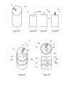
- FIG. 15is an illustration of one embodiment of a Z-directed capacitor comprising semi-cylindrical sheets
- FIG. 16is an exploded view illustration of another embodiment of a Z-directed capacitor comprising stacked discs
- FIGS. 17A-17Cillustrate alternate embodiments of a Z-directed delay line with transparent surfaces to display connections
- FIG. 18illustrates a programmable Z-directed delay line circuit having multiple Z-directed delay lines with transparent surfaces to display connections
- FIGS. 19A-19Cillustrate sectional views of a single conductor differential Z-directed ferrite bead, a 2 conductor differential mode Z-directed ferrite bead, and a 2 conductor common mode Z-directed ferrite bead;
- FIGS. 20A and 20Billustrate a Z-directed switch component that can be rotated to connect predetermined circuit paths in a PCB
- FIG. 20Bis a sectional illustration of the PCB taken along line 20 B- 20 B of FIG. 20A with the Z-directed switch component removed to show internal connection points of the PCB;
- FIG. 20Cis an illustration of the Z-directed switch component of FIG. 20A having an internal electronic component
- FIG. 20Dis a top view of the Z-directed switch component of FIG. 20C showing alternate configurations of the channel shapes and conductive member and radial projections;
- FIGS. 21A-21Dillustrate a Z-directed component utilized for making internal connections between traces on different internal layers or between traces on a given internal layer of a PCB along with an additional feature of a testing path for checking the connections;
- FIGS. 22A and 22Billustrate the use of a plateable side strip and partial insertion of Z-directed components to alter value or function of the Z-directed component
- FIG. 23is an illustration of a system for inserting Z-directed components into a PCB
- FIG. 24is an illustration of a Z-directed component having a glue strip and a glue dot for mounting of the Z-directed component in a PCB;
- FIG. 25is an illustration of a Z-directed component showing copper seed material and resist material used when plating a Z-directed component.
- Z-directed componentsThis specification describes a family of components that are intended to be embedded or inserted into a printed circuit board (PCB). These components are termed Z-directed components and have been modeled and basic prototypes of many of the components described herein, but lacking the surface channels, were made to establish proof of concept. Not all embodiments described herein have been constructed. An overview of how Z-directed components are intended to be formed is presented initially followed by configurations for Z-directed component designs including but not limited to capacitors, delay lines, transistors, switches, and connectors. This is followed by techniques believed to be useful for assembling PCBs with Z-directed components. Z-directed components occupy less space on the surface of a PCB and for high frequency circuits (e.g. clock rates greater than 1000 MHz) allow for higher frequency of operation.
- high frequency circuitse.g. clock rates greater than 1000 MHz
- an X-Y-Z frame of referenceis used.
- the X and Y axesdescribe the plane of a printed circuit board.
- the Z-axisdescribes a direction perpendicular to the plane of the circuit board.
- the top surface of the PCBhas a zero Z-value.
- a component with a negative Z-direction valueindicates that the component is inserted into the top surface of the PCB.
- Such a componentmay be above (extend past), flush with, or recessed below either the top surface and/or the bottom surface of the PCB.
- a component having both a positive and negative Z-direction valueindicates that the component is partially inserted into the surface of the PCB.
- Z-directed componentsare intended to be inserted into a hole or recess in a printed circuit board.
- more than one Z-directed componentmay be inserted into a single mounting hole in the PCB, such as being stacked together or positioned side by side.
- the holemay be a through hole (a hole from the top surface through to the bottom surface) or a well (an opening or recess through either the top or bottom surface into an interior portion or internal layer of the PCB).
- the Z-directed componentsare illustrated as being inserted into the top surface of the PCB.
- one external layeris termed the top surface and the other the bottom surface.
- that external surfaceis referred to as the top surface.
- the Z-directed componentsare referred to as having a top surface, a bottom surface and a side surface.
- the references to top and bottom surfaces of the Z-directed componentconform to the convention used to refer to the top and bottom surfaces of the PCB.
- the side surface of a Z-directed componentis in the Z-direction and would be adjacent to the wall of the mounting hole in the PCB which is also in the Z-direction.
- top, bottom and sideshould not be taken as limiting how a Z-directed component may be mounted into a PCB.
- the componentsare described herein as being mounted in a Z-direction, this does not mean that such components are limited to being inserted into a PCB only along the Z-axis.
- Z-directed componentsmay be mounted normal to the plane of the PCB from the top or bottom surfaces or both surfaces, mounted at an angle thereto or, depending on the thickness of the PCB and the dimensions of the Z-directed component and even inserted into the edge of the PCB between to the top and bottom surfaces of the PCB.
- the Z-directed componentsmay be made from various combinations of materials commonly used in electronic components.
- the signal connection pathswill be made from conductors which are materials that have high conductivity. Conducting materials include, but are not limited to, copper, gold, aluminum, silver, tin, lead and many others.
- Z-directed componentswill have areas that need to be insulated from other areas by using materials that have low conductivity like plastic, glass, FR4 (epoxy & fiberglass), air, mica, ceramic and others.
- a Z-directed component that is constructed as a resistorrequires materials that have properties that are between a conductor and insulator which have a finite amount of resistivity which is the reciprocal of conductivity. Materials like carbon, doped semiconductor, nichrome, tin-oxide and others are used for their resistive properties.
- Capacitorsare typically made of two conducting plates separated by an insulating material that has a high permittivity (dielectric constant). Permittivity is a parameter that shows the ability to store electric fields in the materials like ceramic, mica, tantalum and others. Inductors are typically made of coils of wires or conductors wrapped around a material with high permeability. Permeability is a parameter that shows the ability to store magnetic fields in the material which are iron and alloys like nickel-zinc, manganese-zinc, nickel-iron and others. Transistors and FET are electronic devices that are made from semiconductors that behave in a nonlinear fashion and are made from silicon, germanium, gallium arsenide and others.
- Z-directed componentsmay be constructed of materials that have not been discovered or created to date.
- the body of a Z-directed componentwill in general be comprised of a non-conductive material unless otherwise called out in the description for a particular design of a Z-directed component such as a capacitor.
- the PCB which use a Z-directed componentmay be constructed to have a single conductive layer or multiple conductive layers as is known.
- the PCBmay have conductive traces on the top surface only, on the bottom surface only, on both the top and bottom surfaces.
- one or more intermediate internal conductive trace layersmay also be present in the PCB.
- Connections between a Z-directed component and the traces in or on a PCBmay be accomplished by soldering techniques, screening techniques, extruding techniques or plating techniques as are known in the art. Depending upon application, solder pastes and component adhesives may be used. In some configurations, compressive conductive members may be used to interconnect a Z-directed component to conductive traces found on the PCB.
- a Z-directed componentcomprises a body having a top surface, a bottom surface and a side surface, a cross-sectional shape that is insertable into a mounting hole of a given depth D within a PCB with a portion of the body comprising an insulator. All of the embodiments described herein for Z-directed components are based on this general form.
- FIGS. 1 and 2show an embodiment of a Z-directed component.
- Z-directed component 10comprises a generally cylindrical body 12 having a top surface 12 t , a bottom surface 12 b , a side surface 12 s , and a length L generally corresponding to the depth D of the mounting hole.
- the length Lcan be less than, equal to or greater than the depth D.
- Z-directed component 10would in one case be below at least one of the top and bottom surfaces of the PCB and in the other it would be flush with the two surfaces of the PCB. Where length L is greater than depth D, Z-directed component 10 would not be flush mounted.
- Z-directed component 10would be capable of being used to interconnect to another component or another PCB that is positioned nearby.
- the mounting holeis typically a through-hole extending between the top and bottom surfaces of the PCB but it may also be a blind hole. When recessed below the surface of the PCB additional resist areas may be required in the hole of the PCB to keep from plating the entire circumferential area around the hole.
- Z-directed component 10 in one formmay have at least one conductor 14 extending through the length of body 12 .
- top and bottom conductive traces 16 t , 16 bare provided on the top and bottom end surfaces 12 t , 12 b of body 12 and extend from respective ends of the conductor 14 to the edge of Z-directed component 10 .
- body 12comprises a non-conductive material.
- body 12 of Z-directed component 10may be made of a variety of materials having different properties. These properties include being conductive, resistive, magnetic, dielectric, or semiconductive or various combinations of properties as described herein. Examples of materials that have the properties are copper, carbon, iron, ceramic or silicon, respectively.
- Body 12 of Z-directed component 10may also comprise a number of different networks needed to operate a circuit that will be discussed later.
- One or more longitudinally extending channels or wellsmay be provided on the side surface of body 12 of Z-directed component 10 .
- the channelmay extend from one of the top surface and the bottom surface of body 12 toward the opposite surface.
- two concave wells or channels 18 and 20are provided in the outer surface of Z-directed component 10 extending the length of body 12 . When plated or soldered, these channels allow electrical connections to be made to Z-directed component 10 , through the PCB, as well as to internal conductive layers within the PCB.
- the length of the channels 18 or 20may extend less than the entire length of body 12 .
- FIG. 2shows the same component as in FIG. 1 but with all the surfaces transparent.
- the conductor 14is shown as a cylinder extending through the center of Z-directed component 10 . Other shapes may also be used for conductor 14 .
- Traces 16 t and 16 bcan be seen extending from conductor ends 14 t and 14 b , respectively to the edge of body 12 is a conductor that connects the top trace 16 t to the bottom trace 16 b . While traces 16 t and 16 b are shown as being in alignment with one another (zero degrees apart) this is not a requirement and they may be positioned as needed for a particular design. For example traces 16 t and 16 b may be 180 degrees apart or 90 degrees apart and any all increments therein.
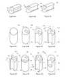
- FIGS. 3A-3Fillustrate possible body shapes for a Z-directed component.
- FIG. 3Ashows a triangular cross-sectional body 40 ;
- FIG. 3Ba rectangular cross sectional body 42 ;
- FIG. 3Ca frusto-conical body 44 ;
- FIG. 3Dan ovate cross sectional cylindrical body 46 ;
- FIG. 3Ea cylindrical body 48 .
- FIG. 3Fis a stepped cylindrical body 50 where one portion 52 has a larger diameter than another portion 54 .
- the Z-directed componentmay be mounted on the surface of the PCB while having a section being inserted into a the mounting hole provided in the PCB.
- the edges of Z-directed componentmay be beveled to help with aligning the Z-directed component for insertion into a through-hole in a PCB.
- Other shapes and combinations of those illustratedmay also be used for a Z-directed component.
- the channels for platingcan be of various cross-sectional shapes and lengths. The only requirement is that plating or solder material make the proper connections to the Z-directed component and corresponding conductive traces in or on the PCB.
- Channels 18 or 20may have, for example, V-, C- or U-shaped cross sections, semi-circular or elliptical cross sections. Where more than one channel is provided, each channel may have a different cross-sectional shape.
- FIGS. 4A-4Cillustrate three channel shapes. In FIG. 4A V-shaped channels 60 are shown. In FIG. 4B , U- or C-shaped channels 62 are shown. In FIG. 4C , wavy or irregular cross-sectional channel shapes 65 are shown.
- the numbers of layers in a PCBvaries from being single sided to being over 22 layers and may have different overall thickness that range from less than 0.051 inch to over 0.093 inch or more.
- the length of the Z-directed componentwill depend on the thickness of the PCB into which it is intended to be inserted.
- the Z-directed component's lengthmay also vary depending on the intended function and tolerance of a process.
- the preferred lengthswill be where the Z-directed component is either flush with the surfaces or extends slightly beyond the surface of the PCB. This would keep the plating solution from plating completely around the interior of the PCB hole that may cause a short in some cases. It is possible to add a resist material around the interior of a PCB hole to only allow plating in the desired areas.
- the number of channels or conductorscan be varied from zero to any number that can maintain enough strength to take the stresses of insertion, plating, manufacturing processes and operation of the PCB in its intended environment.
- the outer surface of a Z-directed componentmay have a coating that glues it in place.
- Flanges or radial projectionsmay also be used to prevent over or under insertion of a Z-directed component into the mounting hole, particularly where the mounting hole is a through-hole.
- a surface coating materialmay also be used to promote or impede migration of the plating or solder material.
- FIG. 5Ais a Z-directed component configured as 0-port device 70 A used as a plug so that if a filter or a component is optional then the plug stops the hole from being plated. After the PCB has been manufactured, the 0-port device 70 A may be removed and another Z-directed component may be inserted, plated and connected to the circuit.
- FIGS. 5B-5Hillustrate various configurations useful for multi-terminal devices such as resistor, diode, transistor, clock circuit.
- FIG. 5Bshows a 1-port or single signal Z-directed component 70 B having a conductor 71 connected to top and bottom conductive traces 72 t , 72 b .
- FIG. 5Cshows a 1-port 1-channel Z-directed component 70 C where one plated well or channel 73 is provided in addition to conductor 71 and top and bottom conductive traces 72 t and 72 b .
- FIG. 5Dshows a Z-directed component 70 D having two wells 73 and 75 in addition to conductor 71 and top and bottom traces 72 t , 72 b .
- the Z-directed component 70 E of FIG. 5Ehas three wells 73 , 75 and 76 in addition to conductor 71 and top and bottom traces 72 t , 72 b .
- FIG. 5Fshows Z-directed component 70 F having two conductors 71 and 77 each with their respective top and bottom traces 72 t , 72 b and 78 t , 78 b and no channels or wells.
- Z-directed component 70 Fis a two signal device to be primarily used for differential signaling.
- FIG. 5Gshows a Z-directed component 70 G having one well 73 and two conductors 71 and 77 each with their respective top and bottom traces 72 t , 72 b and 78 t , 78 b .
- 5Hshows Z-directed component 70 H having one conductor 71 with top and bottom traces 72 t , 72 b and a blind well or partial well 78 extending from the top surface along a portion of the side surface that will allow the plating material or solder to stop at a given depth.
- the number of wells and signalsis only limited by the space, required well size and conductor sizes.
- FIGS. 6A-6Cillustrate examples of such locating features while FIG. 6D illustrates a connection feature.
- Z-directed component 80 Ahas a V-notch 81 on an end surface extending radially outward.
- Z-directed component 80 Bhas a recess 83 on an end surface of Z-directed component 80 B having an orienting surface 84 .
- FIG. 6Cshows Z-directed component 80 C having an axial projection, peg 85 , extending axially outward from an end surface and having an orienting surface 86 .
- An ink mark or other visual or magnetic indicator on a end surface or on the side of a Z-directed componentmay also be used to orient a Z-directed component such as when using a camera.
- Z-directed component 80 Dmay be fitted with a connection feature such as a conductive pad, a spring loaded style pogo-pin or even a simple spring 88 that may be used to add an additional electrical connection (such as frame ground) point to a printed circuit board.
- Spring 88is illustrated as being connected to conductor 89 of Z-directed component 80 D.
- FIGS. 7A and 7Billustrate another configuration for a Z-directed component utilizing O-rings for use in a PCB having a top and bottom conductive layer and at least one internal conductive layer.
- Z-directed component 150is shown having on its top surface 150 t , a locating feature 152 and conductive top trace 154 t extending between conductor 156 and the edge of body 150 d on its top surface 150 t .
- a conductive bottom trace not shownis provided on the bottom surface).
- Conductor 156extends through a portion of the body 150 d as previously described.
- Located on the side surface 150 s of body 150 dis at least one semi-circular channel or grove.
- a pair of axially spaced apart circumferential channels 158 a , 158 bare provided having O-rings 160 a , 160 b , respectively disposed within channels 158 a , 158 b .
- a portion of the O-ringsextend out beyond the side surface 150 s of the body 150 d .
- O-rings 160 a , 160 bwould be positioned adjacent one or more of the internal layers of the PCB to make electrical contact to one or more traces provided at that point in the mounting hole for the Z-directed component. Depending on the design an O-ring would not have to be provided adjacent every internal layer.
- O-rings 160 a , 160 bmay be conductive or non-conductive depending on the design of the circuit in which they are used. O-rings 160 a , 160 b preferably would be compressive helping to secure Z-directed component 150 within the mounting hole.
- the region 162 of body 150 d intermediate O-rings 160 a , 160 bmay be comprised of different material than the regions 164 and 166 of the body 150 d outside of the O-rings. For example if the material of region 162 is of a resistive material and O-rings 160 a , 160 b are conductive, then internal circuit board traces in contact with the O-rings see a resistive load.
- Regions 164 and 166may also be comprised of a material having different properties from each other and region 162 .
- region 164may be resistive, region 162 capacitive and region 166 inductive. Each of these regions can be electrically connected to the adjoining layers of the PCB. Further conductor 156 and traces 154 t , 154 b do not need to be provided. So for the illustrated construction, between the top layer of the PCB and the first internal layer from the top, a resistive element may be present in region 164 , a capacitive element between the first internal layer and the second internal layer in region 162 and an inductive element between the second internal layer and the bottom layer of the PCB in region 166 .
- the signalwould see an inductive load.
- the material for regions 162 , 164 , 166may have properties selected from a group comprising conductive, resistive, magnetic, dielectric, capacitive or semiconductive and combinations thereof.
- the designmay be extended to circuit boards having fewer or more internal layers than that described without departing from the spirit of the invention.
- regions 162 , 164 , 166may have electronic components 167 , 169 , 171 embedded therein and connected as described herein with respect to FIGS. 7-9 .
- a componentmay be found within one or more regions within the body of a Z-directed component.
- Internal connectionsmay be provided from embedded components to O-rings 160 a , 160 b .
- internal connectionsmay be provided from the embedded components to plateable pads provided on the side surface 150 s.
- a Z-directed componentmay be made of a bulk material that performs a network function or may have other parts embedded into its body.
- a Z-directed componentmay be a multi-terminal device, it is clear that it may be used to perform, but not limited to, the following functions: transmission line; delay line; T filter; decoupling capacitor; inductor; common mode choke; resistor; differential pair pass through; differential ferrite bead; diode; ESD protection devices (varistors). Also note that combinations may by be put together within one component.
- FIG. 8illustrates various configurations for a conductor in a Z-directed component.
- conductor 90has a region 92 intermediate the ends comprising a material having properties selected from a group comprising conductive, resistive, magnetic, dielectric, capacitive or semiconductive properties and combinations thereof. These materials form a variety of components. Additionally a component may be inserted or embedded into region 92 with portions of the conductor extending from the terminals of the component. A capacitor 92 a may be provided in region 92 .
- a diode 92 b , a transistor 92 c , a mosfet 92 d , a zener diode 92 e , an inductor 92 f , a surge suppressor 92 g , a resistor 92 h , a diac 92 i and a varactor 92 j and combinations of these itemsare further examples of materials that provided in region 92 of conductor 90 . While region 92 is shown as being centered within the conductor 90 it is not limited to that location.
- one portion of the conductormay be between the top surface trace and to a first terminal of the device, the other portion of the conductor between the bottom surface trace and a second terminal of the device.
- additional conductorsmay be provided in the body of the Z-directed component to allow electrical connection to the remaining terminals or additional conductive traces may be provided within the body of the Z-directed component between the additional terminals and channels on the side surface of the body of a Z-directed component allowing electrical connection to an external conductive trace.
- Various connection configurations to a multiple terminal devicemay be used in a Z-directed component.
- FIGS. 9 and 10illustrate two exemplary connection configurations for a transistor.
- a Z-directed component, 100similar to that shown in FIG. 5F , having two conductors 102 and 104 in body 105 .
- Conductor 102comprising a top portion 102 t , a bottom portion 102 b and an intermediate region 102 i wherein transistor 108 is provided.
- the base 108 b of transistor 108is electrically connected to the top portion 102 t of conductor 102 while the emitter 108 e is connected to the bottom portion 102 b of conductor 102 .
- the collector 108 cis connected to conductor 104 via conductive trace 109 .
- FIG. 9a Z-directed component, 100 , similar to that shown in FIG. 5F , having two conductors 102 and 104 in body 105 .
- Conductor 102comprising a top portion 102 t , a bottom portion 102 b and an intermediate region 102 i wherein transistor
- Z-directed component 110has body 115 including conductor 112 and channel 114 .
- Conductor 112comprises a top portion 112 t , a bottom portion 112 b , and an intermediate region 112 i wherein transistor 118 is provided.
- the base 118 b of transistor 118is electrically connected to the top portion 112 t of conductor 112 while the emitter 118 e is connected to the bottom portion 112 b of conductor 112 .
- the collector 118 cis connected by conductive trace 119 to channel 114 which is plated.
- FIGS. 8 and 9may be extended to additional channels and conductors allowing for use of multi-terminal circuits. The connections are intended only to illustrate how connections to a multi-terminal component may be accomplished and are not meant to limit how a transistor may be connected within a Z-directed component.
- FIGS. 11 and 12illustrating a Z-directed component termed a signal pass-through that is used for passing a signal trace from the top surface of a PCB to the bottom surface.
- FIG. 11shows a sectional view taken along line 11 - 11 in FIG. 12 of a PCB 200 having 4 conductive planes or layers comprising, from top to bottom, a ground (GND) plane or trace 202 , a voltage supply plane Vcc 204 , a second ground GND plane 206 and a third ground GND plane or trace 208 separated by nonconductive material such as a phenolic plastic such as FR4 which is widely used as is known in the art.
- PCB 200may be used for high frequency signals.
- top and bottom ground planes or traces, 202 and 208 respectively, on the top and bottom surfaces 212 and 214 , respectively, of PCB 200are connected to conductive traces leading up to Z-directed component 220 .
- a mounting hole 216 having a depth D in a negative Z directionis provided in PCB 200 for the flush mounting of Z-directed component 220 .
- depth Dcorresponds to the thickness of PCB 200 ; however depth D may be less than the thickness of PCB 200 creating a blind hole therein.
- Mounting hole 216is a through-hole that is round in cross-section to accommodate Z-directed component 220 but may have cross sections to accommodate the insertion of Z-directed components having other body configurations.
- mounting holesare sized so that Z-directed components are insertable therein.
- a Z-directed component having a cylindrical shapemay be inserted into a square mounting hole and vice versa.
- resist materialswill have to be added to the areas of the component and PCB where copper plating is not desired.
- Z-directed component 220is illustrated as a three lead component that is flush mounted with respect to both the top surface 212 and bottom surface 214 of PCB 200 .
- Z-directed component 220is illustrated as having a generally cylindrical body 222 of a length L.
- a center conductor or lead 224illustrated as being cylindrical, is shown extending the length of body 222 .
- Two concave wells or channels 226 and 228are provided on the side surface of Z-directed component 220 extending the length of body 222 .
- Channels 226 and 228are plated for making electrical connections to Z-directed component 220 from various layers of PCB 200 .
- ground plane traces on layers 202 , 206 , and 208 of PCB 100are electrically connected to channels 226 and 228 .
- Vcc plane 204does not connect to Z-directed component 220 as shown by the gap 219 between Vcc plane 204 and wall 217 of mounting hole 216 .
- FIG. 12illustrates a top view of Z-directed component 220 in PCB 200 .
- Three conductive traces 250 , 252 and 254are shown leading up to the edge of wall 217 of mounting hole 216 .
- trace 252serves as a high-frequency signal trace to be passed from the top surface 212 to the bottom surface 214 of PCB 200 via Z-directed component 220 .
- Conductive traces 250 and 254serve as ground nets.
- Center lead or conductor 224is electrically connected to trace 252 on the top surface 212 of PCB 200 by a top trace 245 and plating bridge 230 .
- Top trace 245 on the top surface of Z-directed component 220extends from the top end 224 t of conductor 224 to the edge of Z-directed component 220 .
- the bottom side of Z-directed component 220 and bottom surface 214 of PCB 200is configured in a similar arrangement of traces as shown on top surface 212 of PCB 200 illustrated in FIG. 12 .
- a bottom trace on the bottom surface of Z-directed component 220extends from the bottom of conductor 224 to the edge of Z-directed component 220 .
- a plating bridgeis used to make the electrical connection between the bottom trace and another high frequency signal trace provided on the bottom surface of PCB 200 .
- the transmission line impedance of the Z-directed componentcan be adjusted to match the PCB trace impedance by controlling the conductor sizes and distances between each conductor which improves the high speed performance of the PCB.
- wells 256 and 258 formed between wall 217 of mounting hole 216 and channels 226 and 228allow plating material or solder pass from the top surface 212 to the bottom surface 214 electrically interconnecting traces 250 and 254 , respectively to channels 226 and 228 , respectively, of Z-directed component 220 and also to similarly situated traces provided on the bottom surface 214 of PCB 200 interconnecting ground planes or traces 202 , 206 and 208 .
- the platingis not shown for purposes of illustrating the structure. In this embodiment Vcc plane 204 does not connect to Z-directed component 220 .
- a Z-directed signal pass through componentmay also comprise a decoupling capacitor that will allow the reference plane of a signal to switch from a ground plane, designated GND, to a voltage supply plane, designated V CC , without having a high frequency discontinuity.
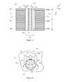
- FIG. 13shows a cross-sectional view of a typical 4-layer PCB 300 with a signal trace 302 transferring between the top layer 304 and the bottom layer 306 .
- Z-directed component 310similar to that shown in FIG. 5D , having body 312 connects signal trace 302 through center conductor 314 .
- Z-directed component 310also comprises plated channels 316 and 318 extending along the side surface 312 s of the body 312 .
- top 314 t and bottom 314 b of conductor 314are connected to conductive traces 318 t and 318 b on the top 312 t and bottom 312 b of body 312 . These in turn are connected to signal trace 302 via top and bottom plating bridges 330 t and 330 b .
- Channels 316 and 318will be plated to GND plane 332 and Vcc plane 334 , respectively.
- Connection points 336 and 338respectively, illustrate this electrical connection.
- Schematically illustrated decoupling capacitor 350is internal to body 312 and is connected between channels 316 and 318 .
- Decoupling capacitor 350may be a separate capacitor integrated into the body 312 of Z-directed component 310 or it can be formed by fabricating a portion of the body 312 of Z-directed component 310 from the required materials with dielectric properties between conductive surfaces.
- the path for signal trace 302is illustrated with diagonal hatching and can be seen to run from top layer 304 to bottom layer 306 .
- GND plane 332 and channel 316are electrically connected at 336 with the signal path return indicated by the dark stippling 362 .
- Vcc plane 334 and channel 318are electrically connected at 338 with the signal path return indicated by the light stippling 364 As is known in the art where a signal plane or trace is not to be connected to the inserted part those portions are spaced apart from the component as shown at 370 .
- the signal plane or traceis provided at the wall or edge of the opening to allow the plating material or solder to bridge therebetween as illustrated at points 330 t , 330 b , 336 , and 338 .
- the vertically hatched portion 380shows the high speed loop area between the signal trace and return current path described by the signal trace 302 and the GND plane 332 or Vcc plane 334 .
- the signal trace 302 on the bottom surface 306is referenced to power plane Vcc 334 that is coupled to the GND plane 332 through decoupling capacitor 350 . This coupling between the two planes will keep the high frequency impedance close to constant for the transition from one return plane to another plane of a different DC voltage.
- FIG. 14illustrates one embodiment of this technique.
- PCB 400is comprised of, from top to bottom, top ground layer 402 , internal signal layer 404 , internal signal layer 406 and bottom ground layer 408 .
- Ground layers 402 and 408are on the top and bottom surfaces 400 t and 400 b of PCB 400 .
- a mounting hole 410 shown as a through-holeextends between the top and bottom surfaces 400 t and 400 b .
- Z-directed component 420is shown flush mounted in PCB 400 .
- Z-directed component 420comprises body 422 having a center region 424 intermediate the top 422 t and bottom 422 b of body 422 and two channels 425 and 427 on side surface 422 s.
- the channels 425 and 427 and wall 411 of hole 410form plating wells 413 and 415 respectively.
- Center region 424is positioned within body 422 and extends a distance approximately equal to the distance separating the two internal signal layers 404 and 406 .
- Channel 425extends from the bottom surface 422 b of body 422 to internal signal level 406 while channel 427 extends from top surface 422 t of body 422 to internal signal level 404 .
- channels 425 and 427extend only along a portion of side surface 422 s of body 422 .
- Conductor 426extends through center region 424 but does not extend to the top and bottom surfaces 422 t , 422 b of body 422 .
- FIG. 5Hillustrates a partial channel similar to channel 427 .
- Conductor 426has conductive traces 428 t and 428 b extending from the top 426 t and bottom 426 b of conductor 426 to channels 427 and 425 , respectively. While illustrated as separate elements conductor 426 and traces 428 t , 428 b may be one integrated conductor electrically interconnecting channels 425 , 427 . As shown conductive trace 428 b is connected to internal signal layer 406 via plated channel 425 and well 413 while trace 428 t connects to internal signal level 404 via channel 427 and well 415 . Ground layers 402 and 408 are not connected to Z-directed component 420 and are spaced away from mounting hole 410 as previously described for FIGS. 11 and 13 .
- a signal on signal layer 406can be via'd to signal layer 404 (or vice versa) via Z-directed component through a path extending from well 413 , channel 425 , trace 428 b , conductor 426 , trace 428 t , channel 427 , and well 415 to allow the signal to remain on the inner layers of PCB 400 with ground layers 402 and 408 providing shielding.
- Capacitors having a Z-directed component body typemay be constructed in several ways.
- a Z-directed capacitor 500is shown with body 502 having a conductor 504 and two channels 506 and 508 extending its length similar to those previously described.
- Conductor 504is shown connected to a signal 526 .
- Vertically oriented interleaved partial cylindrical sheets 510 , 512 forming the plates of Z-directed capacitor 500are connected to reference voltages such as voltage Vcc and ground (or any other signals requiring capacitance) are used with intervening layers of dielectric material (not shown).
- Partial cylindrical sheet 510is connected to plated channel 506 which is connected to Ground 520 .
- Partial cylindrical sheet 512is connected to plated channel 508 that is shown connected to supply voltage Vcc 522 .
- the sheets 510 , 512may be formed of copper, aluminum or other material with high conductivity.
- the material between the partial cylindrical sheetsis a material with dielectric properties. Only one partial cylindrical sheet is shown connected to each of Vcc 522 and ground 520 , however additional partial cylindrical sheets may be provided to achieve the desired capacitance/voltage rating.
- Z-directed capacitor 600is comprised of center conductor 601 , and a body 605 comprised of a top member 605 t , a bottom member 605 b , plurality of support members 610 (illustrated as disks) between the top and bottom members 605 t , 605 b.
- Center conductor 601extends through openings 615 in the assembled Z-directed capacitor 600 and openings 602 t and 602 b , all of which are sized to closely receive the center conductor.
- the center conductoris electrically connectable to conductive traces 603 t and 603 b on the top and bottom portions 605 t , 605 b forming a signal path for signal 626 . This connection is made by plating or soldering.
- Conductor 601is connected to signal 626 via conductive trace 603 t .
- the bottom end of conductor 601is connected in a similar fashion to a signal trace (not shown) via conductive trace 603 b.
- Opposed openings 607 t and 608 tare provided at the edge on top portion 605 t .
- Bottom portion 607is of similar construction as top portion 605 having opposed openings 607 b and 608 b provided at the edge.
- Between top and bottom portions 605 , 609are a plurality of support members 610 , which provide the capacitive feature.
- Support members 610each have at least one opening 613 at their outer edge and an inner hole 615 allowing for passage of conductor 602 therethrough. As shown two opposed openings 613 are provided in each support member 610 .
- the opposed openings 607 t , 607 b , 608 t , 608 b , and 613align to form opposed channels 604 and 608 extending along the side surface of Z-directed capacitor 600 .
- Channel 604is shown connected to reference voltage such as ground 620 and channel 606 to another reference voltage such as Vcc 622 .
- Support members 610may be fabricated from a dielectric material and may be all of the same or varying thickness allowing for choice in designing the desired properties for Z-directed capacitor 600 .
- Annular plating 617is provided on one of top and bottom surfaces of support member 610 or if desired on both surfaces. As shown annular plating is shown on the top surface of each support member but location of the annular plating can vary from support member to support member. Annular plating 617 generally conforms to the shape of the support member and extends from one of the edge opening 613 toward the other if an additional opening is provided. The annular plate 617 is of a diameter or dimension or overall size that is less than the diameter, dimension or overall size of support member 610 on which it is affixed. While the plate 617 is described as annular, other shapes may also be used provided that the plating does not contact the center conductor or extend to the edge of the support member on which it is plated or otherwise affixed.
- the annular platedoes contact one of the edge openings 613 but is spaced apart from the other openings, if more than one channel is present in the side surface of the body of Z-directed capacitor 600 . Also there is an opening 619 in annular plate 617 having a larger diameter than opening 615 in annular plate 617 through which conductor 601 passes. Opening 619 has a larger diameter than that of conductor 602 leaving annular plate 617 spaced apart from conductor 602 .
- the support members 610are substantially identical except that when stacked alternate members are rotated 180 degrees with respect to the member above or below it. This may be referred to as a 1-1 configuration. In this way, alternate members will be connected to one or the other of the two channels. As shown in FIG. 16 , the annular plating on the upper one of the two support members 610 is connected to channel 608 and voltage Vcc 622 while the annular plating on the lower one of the two support members 610 is connected to channel 604 and ground 620 . Other support member arrangements may also be used such as having two adjacent members connected to the same channel with the next support member being connected to the opposite channel which may be referred to as a 2-1 configuration. Other configurations may include 2-2, 3-1 and are a matter of design choice.
- the desired capacitance or voltage ratingdetermines the number of support members that are inserted between top and bottom portions 605 , 609 .
- dielectric memberscomprised of dielectric material and similarly shaped to support members 610 may be interleaved with support members 610 .
- the annular platingmay be brought into contact with the center conductor and not in contact with the channels.
- a second conductormay be provided in parallel with the first conductor that is disposed within the conductive plates to create a differential decoupling capacitor.
- Another embodiment of a Z-directed capacitorcan be constructed from FIG. 15 or FIG. 16 by connecting center conductor to one of the reference voltages at each support member that also has its annular plating connected to the same reference voltage. This may be accomplished simply by connecting the conductor to the annular plating as schematically illustrated by the jumper 621 .
- the annular opening 619 in the annular plate 617would be sized so that the annular plate and conductor 602 would be electrically connected. This component may be placed directly below a power pin or ball of an integrated circuit or other surface mounted component for optimum decoupling placement.
- FIGS. 17A-17C and 18illustrate embodiments of Z-directed signal delay line component.
- a Z-directed signal delay linecomprises a body having a signal conductor routed therein with the signal conductor made from one of a dielectric material, and a magnetic material that slows down signals that travel through the delay line.
- the signal conductorhas a length contained within the body and may be of the same length as the length of the body or may be longer in length than the length of the body. Connections to the signal conductor may be made via channels provided on the side surface of the Z-directed component or to conductive traces provided on the top and or bottom surfaces or by a combination of top and/bottom traces and channels.
- Z-directed component 700 Ahas a body 702 having conductive traces 703 a and 703 b on its top surface 702 t .
- delay line 704Disposed within body 702 a is delay line 704 comprised of a plurality of conductive legs comprising vertically oriented segments 704 a - 704 d extending along a portion of the length of body 702 a and connected by a plurality of short horizontal bars 704 e in a serial fashion at their respective top and bottom ends (roughly approximating a W-shape) forming the delay line 704 in an undulating or a zigzag manner.
- the top ends of segments 704 a and 704 dare shown connected to conductive traces 703 a and 703 b respectively on the top surface 702 t of the body 702 a .
- the additional length of the conductor forming delay line 704 inserted into a signal pathcauses the signal to travel a longer distance therefore delaying it.
- the connection to delay line 704may also be accomplished using a channel provided in the side 702 s of body 702 a either in combination with conductive traces on the top or bottom surfaces or in lieu of top and bottom conductive traces. Additional segments may be added to delay line 704 to increase the amount of delay.
- a Z-directed component delay line 700 Bhas a body 702 with conductive traces 703 t and 703 b on the top and bottom of body 702 b .
- delay line 705comprised of a plurality of horizontally disposed (as viewed in FIG. 16B ) C-shaped conductors 705 a - 705 d spaced apart from one another and serially connected by a plurality of vertical leg segments 705 e .
- the C-shaped conductors 705 a - 705 dmay also be described as being disposed approximately parallel to the top or bottom surfaces, 702 t , 702 b of the body 702 and the leg segments 705 as approximately parallel to the side surface of the body.
- leg segments 705 e adjacent the top and bottom of body 702 bconnect to traces 703 c and 703 d on the top and bottom surfaces. Again the additional length of delay line 705 inserted into a signal path causes the signal to travel longer, delaying it. If there is excessive capacitive coupling between adjacent C-shaped conductors then a shielding material (not shown) may be disposed within body 702 between adjacent C shaped conductors and grounded. It is expected that this should remove most of the parasitic effects of this geometry. The connections between adjacent C-shaped conductors are made such that the magnetic flux of one C-shaped conductor cancels the next. This reduces the magnetic coupling between the C-shaped conductors. Additional C-shaped conductors may be added to increase the delay. Alternatively, the delay line may be arranged in a spiral configuration.
- FIG. 17Cillustrates a programmable version of the Z-directed delay line of FIG. 17B .
- Z-directed delay 700 Chas body 702 b having top and bottom traces 703 t .
- Delay line 705 disposed within body 702 bis comprised of a plurality of serially connected C-shaped conductors as previously described.
- a shorting mechanise for the C-shaped conductorsis disposed within or on the body 702 b and may be comprised of at least one shorting bar. By selectably removing portions of the shorting bar between adjacent C-shaped conductors the amount of delay provided by Z-directed component delay line 700 C may be adjusted or programmed. As illustrated two drillable shorting bars 708 , 709 are shown and used to program the delay time of the part.
- shorting bars 708 , 709extend along the length of the body 702 b and tangentially contact each of the C-shaped conductors.
- the shorting bars 708 and 709are diametrically opposed to one another such that a line drawn between them would bisect each C-shaped conductor 705 a - 705 d . If the minimum delay is desired then shorting bars 708 , 709 are left in place. If the maximum delay is desired then shorting bars 708 , 709 are removed by drilling or etching the conductive material away. As portions of shorting bars 708 , 709 are removed between adjacent C-shaped conductors, the time delay will increase by 1 ⁇ 2 or whole turn increments at a time. This can be used in development to easily determine the best signal delay for production purposes. Also each PCB may be tuned during functional testing to optimize the delay of signals to compensate for variation of other parameters in a design.
- One or more shorting barsmay also be used with Z-directed delay line 700 A by placing the shorting bar horizontally across the vertical conductor segments 704 a - 704 d as indicated by the line 710 .
- the time delaywould have to be adjusted prior to insertion of the part into a PCB.
- one or more channelsmay be provided as a shorting mechanism in lieu of shorting bars and by use of selective plating techniques in plating such Z-directed delay lines portions of delay lines 704 or 705 may be shorted together.
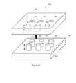
- variable delay line 730may be created by connecting any number of Z-directed delay lines together by conductive traces on a PCB. These surfaces are shown as transparent to illustrate the connections.
- cylinders 750 , 760 , and 770Inserted in PCB 740 are cylinders 750 , 760 , and 770 which can represent either a Z-directed delay line, as illustrated in FIGS. 17A-17C , or a conductive plug or Z-directed signal pass through component and which are connected in series fashion by top and bottom conductive traces 780 t , 780 b as shown on the top and bottom surfaces 740 t , 740 b of PCB 740 .
- Cylinders 750 , 760 and 770may also be connected serially via conductive traces provided on internal layers of PCB 740 if present or by a combination of internal or external conductive traces. If cylinders 750 , 760 and 770 each represent a Z-directed delay line element, then total delay across delay line 730 may be changed by replacing a Z-directed component delay line elements with a Z-directed component signal pass through device, previously described, that introduces no significant delay or with another Z-directed component delay line having a greater delay.
- One advantage of this configurationis that no changes are required to the PCB layout design while still allowing the total signal delay to be adjusted.
- a Z-directed T filter and a Z-directed Pi filterare three port devices having an input conductor, output conductor and a ground conductor.
- T filtersare generally comprised of, for a low pass filter, two serial resistors connected between an input and an output with a capacitor connected between the resistors and to ground or, for a high pass filter, two serial capacitors connected between the input and an output and a resistor connected between the capacitors and to ground. Schematically these filters resemble the letter T.
- Pi filtershave one component connected between input and output with a second component connected between input and ground and a third component connected between the output and ground. The first component may be a resistor and the second and third component may be capacitors and vice versa. Inductors may also be used. These devices may be mounted in a Z-directed component in a similar fashion as the transistor shown FIGS. 8 and 9 .
- FIGS. 19A-19Cillustrate cross-sectional views of alternate embodiments of Z-directed ferrite beads.
- the construction of these devicesis similar to that shown and described in FIGS. 5B-5H .
- a cylinder 1001 of magnetic materialhaving an opening through which conductor 1002 passes.
- the conductor 1002extends to the top and bottom surfaces of the body 1000 where it is electrically connected to top and bottom traces.
- the conductormay also be connected as previously described such as to a channel on the side surface of the body or two side channels etc.
- By varying the outside diameter cylinder 1001the magnetic properties are varied controlling the characteristics of the ferrite bead.
- cylinder 1001is contained within body 1000 but its outer circumference may also extend to the side surface of body 1000 . This construction creates a single conductor differential Z-directed ferrite bead.
- two conductors 1002 - 1 and 1002 - 2pass through two openings provided in cylinder 1001 in the body 1000 forming a two conductor differential mode Z-directed ferrite bead.
- the two parallel spaced apart conductors 1002 - 1 and 1002 - 2are enclosed by cylinder 1001 comprised of magnetic material.
- cylinder 1001comprised of magnetic material.
- the magnetic propertiesare varied controlling the characteristics of the ferrite bead.
- cylinder 1001is contained within body 1000 but its outer circumference may also extend to the side surface of body 1000 .
- FIG. 19CShown in FIG. 19C , is a two conductor common mode Z-directed ferrite bead that is substantially similar to a two conductor differential mode Z-directed ferrite bead but with both of the conductors 1002 - 1 , 1002 - 2 within the cylinder 1001 a passing through a common opening 1003 in the magnetic material forming cylinder 1001 a .
- the volume within opening 1003is not filled with magnetic material.
- the volumemay be left empty, i.e. air filled, or another nonmagnetic material may be used to filled the portion not filled by conductors 1002 - 1 , 1002 - 2 .
- FIGS. 20A and 20Billustrate a PCB 1101 having a multiplicity of internal layers 1102 having one or more conductive traces and a multiplicity of conductive surface traces 1103 , three of which are further designated as a, b and c, on outer surface 1104 . Conductive traces may be provided on both outer surfaces of PCB 1101 .
- Z-directed component 1105is mounted in mounting hole 1106 shown as a through hole. A channel 1107 of Z-directed component 1105 is shown aligned with circuit trace 1103 a .
- the channel 1107extends along the side surface 1105 from the top surface 1105 t to bottom surface 1105 b .
- the length of the channelmay be less than the length of the body of the Z-directed component and may extend only from one of the top and bottom surfaces toward the other or may be disposed intermediate the top and bottom surfaces such as, for example, extending only between the two internal layers of PCB.
- Shown inserted into channel 1107is a compressive conductive member, such as rod 1109 .
- a compressive conductive membersuch as rod 1109 .
- a compressive conductive membersuch as rod 1109 .
- turning structuresuch as slot 1108 used to rotate Z-directed component 1105 into alignment with the desired surface trace 1103 .
- Other configurationssuch as a pair of holes or a cross-shaped slot may also be used in lieu of slot 1108 .
- FIG. 20Bis a sectional view taken along line 20 B- 20 B of FIG. 20A with Z-directed component 1105 removed, a multiplicity of internal connection points 1110 - 1113 are shown.
- connection between trace 1103 a and connection point 1110is made as indicated by the dashed line interconnecting these two points.
- trace 1103 bwill be connected to connection point 1111 as indicated by the dashed line interconnecting these two points.
- trace 1103 cwill be connected to connection points 1112 and 1113 as indicated by the dashed line shown interconnecting these three points.
- the compressive conductive memberWhen the compressive conductive member is a rod it may have a diameter that is less than and preferably equal to or greater than the diameter of channel 1107 .
- compressive conductive rod 1109is shown having a diameter that is larger than the diameter of channel 1107 . This is done to ensure that compressive rod 1109 will be compressed when inserted in channel 1107 helping to ensure that compressive conductive rod 1109 will be retained within the body of Z-directed component 1105 due to the interference fit between the rod and channel. Further, as illustrated in FIG.
- channel 1107is positioned at the edge of Z-directed component 1105 so that the center line 1109 a of compressive conductive rod 1109 will be positioned at a distance that is within or less than the radius R of Z-directed component 1105 while still allowing a strip 1109 s of the outer side surface of compressive conductive rod 1109 to extend beyond the side surface 1105 s of Z-directed component 1105 to make the desired electrical connections.
- This strip or portion 1109 s of the outer peripheryis exaggeratedly shown in FIG. 20D . It is expected that this will also aid in keeping Z-directed component 1105 inserted into PCB 1101 .
- Additional channels and compressive conductive rodsmay also be provided in Z-directed component 1105 and arranged about the periphery of Z-directed component 1105 as needed to meet the design requirements for the circuit forming a multi-pole switch.
- compressive rod 1109having a diameter that is less than the diameter of channel 1107 shims or other means such as raised portions in the channel wall inserted between the channel surface and the compressive conductive rod may be used to ensure the compressive conductive rod will have a portion extending beyond the side surface 1105 s of Z-directed component 1105 .
- channel 1120is generally triangular or trapezoidal in section with the open apex aligned with the side surface. Shown inserted in channel 1120 is a generally rectangular compressive conductive member 1122 which has pinched-in waist 1122 w caused by the sectional shape of channel 1120 . Member 1122 may also have a triangular section as well.
- Z-directed component 1105in this manner allows PCB 1101 to be configured with an identification indicia such as a serial number using a minimal number of components. Connections between the surface layers of PCB 1101 (either top surface, bottom surface or both) can also be made to inner layers by the use of a well provided in Z-directed component 1105 as previously described. Further one or more wells and one or more center conductors may be used to provide for a multiplicity of connections between and among the internal layers 1102 and surface layers of PCB 1101 .
- Z-directed component 1105may also be removably inserted into mounting hole 1106 allowing for it to be realigned similar to a single-gang or multi-gang rotary switch, depending on the number of layers in PCB 1101 .
- a slotmay be provided in one of the end surfaces of Z-directed component to allow it to be rotated by a screwdriver or other similar means.
- the top surface 1105 tmay have radial projections 1130 or a flange that can be used to prevent the Z-directed component from sliding out of the mounting hole when being rotated.
- the Z-directed component 1105may have a number of different circuits or values of components, indicated by dashed block 1115 in FIG. 20C , incorporated into the body thereof and be used to connect one or more traces on a layer of the PCB (interior or exterior layer) with another one or more traces on the same or other surfaces in the PCB using channels or conductors as previously described.
- different circuitscan be selected by rotating the part to select which conductor(s) is/are bridged that have the desired circuit component between 2 or more connection points.
- one Z-directed componentmay have a range of resistive values therein that are selected by inserting the Z-directed component and aligning it with the desired conductive traces.
- the conceptmay be expanded to any combination of electronic components that will fit within the volume of the body of the Z-directed component along with the necessary conductive traces.
- FIGS. 21A , 21 C, and 21 Dillustrate another configuration of an internal Z-directed component connector that can make the internal connections without the need for this back drilling process. This embodiment also illustrates the use of test paths with the body of the Z-directed component. This interior connector may be used anytime a plating well is not desired to the top or bottom layers of a PCB.
- a Z-directed component 1200has at least two recessed areas or pockets 1202 a , 1202 b , 1202 c , 1202 d on the side surface 1200 s that will contain a solder paste material (not shown) that will either expand or reflow when heated to make the desired connections.
- a conductor 1216 a , 1216 b , 1216 c , 1216 dis provided between top surface 1200 t and each of pockets 1202 a - 1210 d , respectively.
- the portions 1216 a 1 - 1216 d 1 of conductors 1216 a - 1216 d on surface 1200 tmay be used as test points by test probes as described herein.
- FIG. 21BShown in the FIG. 21B is a sectional view of a four-layer PCB 1210 having two internal layers 1211 a , 1211 b , each having two conductive signal traces 1212 a and 1212 b , 1212 c and 1212 d , respectively, provided at four internal locations in the wall 1214 w of mounting hole 1214 .
- trace 1212 ato trace 1212 c and trace 1212 b to trace 1212 d
- Other numbers of internal layers and signal tracesmay also be connected in a similar fashion using an appropriately designed Z-directed component internal connector.
- Z-directed component 1200four correspondingly positioned pockets 1202 a - 1202 d are positioned on side surface 1200 s so that when Z-directed component 1200 is inserted into mounting hole 1214 these pockets will be adjacent to traces 1212 a - 1212 d respectively on internal layers 1211 a , 1211 b.
- the pocketsmay be interconnected by a variety of means as is known in the art. Two examples are illustrated in FIGS. 21A and 21C .
- Oneis a channel 1220 cut into side surface 1200 s interconnecting pockets 1202 b and 1202 d that may be filled with solder paste or into which the solder paste in the pockets will flow when heating of the PCB occurs. Additional channels interconnecting all of the pockets together can be provided and the pockets may be selectably interconnected by use of removable dams indicated by dashed lines 1224 provided in the channel 1220 . This permits the interconnections to be determined after the Z-directed connector has been fabricated. Where a connection is desired between two pockets the dam 1224 in the channel interconnecting these pockets would be removed.
- the other connectionmay be done by a conductor 1222 provided in the body 1200 b interconnecting pockets 1202 a and 1202 c .
- the manner of the interconnectionwould need to be predetermined so that the conductors are positioned between the desired interconnection points.
- test probes placed on test points 1216 a 1 - 1216 dFor the illustrated pairs of connections only a single test point is needed for each pair of interconnected pockets; however it may be desired to have a test point for each connection pocket as shown.
- FIGS. 21C and 21Dshow Z-directed component internal connect 1200 having an optional multi-terminal component 1230 either embedded or formed within the body 1200 b .
- Component 1230may be an active or passive component may also be inserted in the connection path to the internal layers 1211 a , 1211 b of PCB 1210 .
- one terminal of component 1230is connected to top surface 1200 t of Z-directed component 1200 via conductor 1232
- a second terminalis shown connected to pocket 1202 a via conductor 1234
- a third terminal of component 1230is shown connected to pocket 1202 d via conductor 1236 .
- Components having more or less terminalsmay also be accommodated within Z-directed component 1200 depending on volume available for the internal component and conductors.
- test paths 1216 a - 1216 dmay not be present in some designs. However, the testing paths may be used with any of the Z-directed parts described herein to improve testability. Also the top and or bottom surface of this Z-directed component may have a conductive coating substantially coextensive with the surface to provide further shielding when the Z-directed component is installed and plated in a PCB.
- a Z-directed componentmay work best when partially inserted into the PCB.
- a Z-directed componentmay have a parameter, such as resistivity that can be controlled by the depth that it is inserted into the PCB.
- resistivitysuch as resistivity
- One examplewould be a resistor that normally has a fixed resistive value between the top and bottom surfaces by applying a uniform resistive film over the side surface of the body This is illustrated in FIGS. 22A and 22B illustrating a PCB 1300 having a Z-directed resistor 1320 inserted at two different depths into a mounting hole 1302 indicated by the dashed lines.
- the PCB 1300is illustrated as having signal traces 1303 , 1305 on one external surface, top surface 1300 t and signal traces 1307 , 1309 on the other external surface, bottom surface 1300 b .
- Z-directed resistor 1320interconnects signal trace 1303 to signal trace 1305 .
- Two internal layersare shown for PCB 1300 , a first voltage reference layer Vcc 1311 , and a second voltage reference layer GND 1313 .
- Side surface 1330 s of body 1330has two closed end or blind channels, 1332 , 1334 extending from top surface 1330 t . These blind channels could also both extend from the bottom surface 1330 b .
- a plateable strip 1340is shown disposed on side surface 1330 s of body 1330 between the top and bottom surfaces 1330 t , 1330 b . Disposed within body 1330 are conductors 1335 , 1336 electrically connected to respective ends of plateable strip 1340 . The other ends of conductors 1335 , 1336 are electrically connected to channels 1332 , 1334 .
- Line 1350indicates the position of top surface 1300 t with respect to body 1330 .
- Z-directed resistor 1320is inserted into mounting hole 1302 a depth D 1 where portion P 1 represents the portion of plateable strip 1340 below the top surface 1300 t of PCB 1300 and portion P 2 represents the portion of plateable strip 1340 above.
- the exposed side surface 1300 s above the top surface 1300 t along with portion P 2 of plateable strip 1340would be plated with copper shorting out the portion P 2 and reducing the overall resistance of Z-directed resistor 1320 .
- the channels 1332 , 1334are closed ended to prevent the plating material from shorting the two channels together.
- Z-directed resistoris shown inserted at a greater depth D 2 . Accordingly on plateable strip 1340 portion P 1 has increased and portion P 2 has decreased. At insertion depth D 2 and after plating has occurred, the overall resistive value of Z-directed resistor 1320 is greater than that when inserted at depth D 1 .
- This conceptmay be used with any passive element that can have its value adjusted by plating over part of a surface.
- a Z-directed inductorwherein portions of the windings are exposed along the length of the side surface.
- a Z-directed capacitorhaving stacked disks similar to those as shown in FIG. 15 but modified so as not to have the annular plate 617 connected to either of the side channels 604 , 608 . Instead one or more of the annular plates 617 would be electrically connected to a corresponding conductor disposed within the body 605 with the other end of the conductor being exposed on the side surface of the body 605 .
- a further exampleis a signal delay line such as that shown in FIG.
- FIG. 7BAnother use for this partial insertion technique would be where different electronic functions exist in regions between the top and bottom surfaces of the body of the Z-directed component. As shown in FIG. 7B multiple devices or circuits may be provided in the body 150 . Internal connections may be provided to plateable pads provided in the side surface. The exposed pads would be shorted out by the copper plating in a similar way to the resistor example. As discussed later, a Z-directed component can be adjusted after the PCB has been manufactured. A circuit design may call for a Z-directed component providing an optional function or feature to the circuit to be partially inserted into the PCB and make no connections at the time of manufacturing. Later if the Z-directed component is needed to add its new function to the circuit in the PCB it would be pushed into place while in the field.
- the strip used in a Z-directed variable value componentmay also have one or more etchable portions 1360 having a conductor connected to each end of the strip (see FIG. 22A ).
- the conductorsmay be internal to the body of the component, provided on an external surface or be a combination of external and internal connects as previously shown and described.
- the value of the Z-directed variable value componentwould be adjusted by selectively etching away etchable portions 1360 of the strip while still maintaining a signal path between the two end conductors. For example, if the strip were comprised of a resistive material, removal of some of this material by etching would decrease the value of the resistance. Depending on the material within the etchable portions the value of the component may increase or decrease as the material is etched away. Depending on the depth to which such a component is mounted in the PCB, fewer or more of the etchable portions would be exposed to etching.
- an insertion system 800comprising an orienting fixture 802 and ram plate 804 as shown in FIG. 23 .
- orienting fixture 802Positioned on orienting fixture 802 are one or more Z-directed components 806 .
- Orienting fixture 802 using locating surfaces or other indicia provided on Z-directed components 806 ram plateorients these components for insertion into PCB 850 shown positioned over orienting fixture 802 and having one or more mounting holes 852 for receiving Z-directed component 806 therein as previously described.
- PCB 850is held by a fixture not shown.
- mounting holes 852are through-holes and the depth D of the holes corresponds to the length L of Z-directed components 806 .
- the length Lmay be less than, equal to or greater than depth D allowing for recessed mounting, flush mounting or extended mounting.
- resist materialwill be needed to ensure that only those portions of the recessed surface that are to be plated will be plated and to avoid plating of the entire recessed surface.
- Ram plate 804is raised as indicated by arrow 860 inserting Z-directed components 806 into corresponding mounting holes 852 in PCB 850 through the bottom surface of PCB 850 .
- the ram platemay have cylinders that press each component 806 through the orienting fixture 802 into mounting holes 852 to the correct depth. These cylinders may be individually operated or any combination at one time.
- insertion equipmentthat orientates the part and inserts them into the PCB will be needed.
- pick and place equipmentmay also be used to insert a Z-directed component into a PCB.
- Such pick and place equipmentmay insert a Z-directed component from either the top or bottom surface of a PCB.
- a plunger devicewill be needed to press the Z-directed component into the PCB to the desired insertion depth.
- Z-directed componentsmay be press fit or glued in place in a PCB.
- the PCB and Z-directed component interfacecan include resist material to prohibit plating or seed material to help facilitate plating. Examples are shown in FIGS. 24 and 25 .
- a Z-directed component 900having a body 902 and two channels 904 a and 904 b extending along side surface 902 s and a conductive top trace 906 is shown having a glue strip 910 or a glue dot 911 on side surface 902 s allowing Z-directed component 900 to adhere to the wall of a mounting hole in a PCB prior to plating.
- a Z-directed component 920having a body 922 and two channels 924 a and 924 b extending along side surface 920 s and a conductive top trace 926 is shown having copper seed material 927 indicated by the horizontal lines on channels 924 a , 924 b conductive trace 926 with resist material 928 indicated by the angled lines on the remaining portions of side surface 902 s .
- Compliant materialsmay be used to keep plating material from migrating past desired locations. For parts that extend past the surface of the PCB, the seed copper may be taken around the edge of a Z-directed component down the side surface to the surface of the PCB.
- Other surface mount partsmay be mounted over the part and may even have pads or balls to have surface mount parts connected directly to them.
- the ballsmay be attached directly to the top surface of a Z-directed component.
- Z-directed componentsmay also be contained in a tape and reel packaging material.
- a partcan be extracted using a pick and place vacuum head and be partially inserted in to a PCB.
- a cameracan then be used to check the orientation of the Z-directed component and the Z-directed component position adjusted before being fully inserted into the PCB.
Landscapes
- Engineering & Computer Science (AREA)
- Power Engineering (AREA)
- Microelectronics & Electronic Packaging (AREA)
- Manufacturing & Machinery (AREA)
- Structures For Mounting Electric Components On Printed Circuit Boards (AREA)
- Structure Of Printed Boards (AREA)
Abstract
Description
Claims (4)
Priority Applications (3)
| Application Number | Priority Date | Filing Date | Title |
|---|---|---|---|
| US12/508,145US8198547B2 (en) | 2009-07-23 | 2009-07-23 | Z-directed pass-through components for printed circuit boards |
| US13/349,822US8829358B2 (en) | 2009-07-23 | 2012-01-13 | Z-directed pass-through components for printed circuit boards |
| US14/475,656US9984820B2 (en) | 2009-07-23 | 2014-09-03 | Z-directed capacitor components for printed circuit boards |
Applications Claiming Priority (1)
| Application Number | Priority Date | Filing Date | Title |
|---|---|---|---|
| US12/508,145US8198547B2 (en) | 2009-07-23 | 2009-07-23 | Z-directed pass-through components for printed circuit boards |
Related Child Applications (1)
| Application Number | Title | Priority Date | Filing Date |
|---|---|---|---|
| US13/349,822DivisionUS8829358B2 (en) | 2009-07-23 | 2012-01-13 | Z-directed pass-through components for printed circuit boards |
Publications (2)
| Publication Number | Publication Date |
|---|---|
| US20110019375A1 US20110019375A1 (en) | 2011-01-27 |
| US8198547B2true US8198547B2 (en) | 2012-06-12 |
Family
ID=43497161
Family Applications (3)
| Application Number | Title | Priority Date | Filing Date |
|---|---|---|---|
| US12/508,145Expired - Fee RelatedUS8198547B2 (en) | 2009-07-23 | 2009-07-23 | Z-directed pass-through components for printed circuit boards |
| US13/349,822ActiveUS8829358B2 (en) | 2009-07-23 | 2012-01-13 | Z-directed pass-through components for printed circuit boards |
| US14/475,656Active2030-08-25US9984820B2 (en) | 2009-07-23 | 2014-09-03 | Z-directed capacitor components for printed circuit boards |
Family Applications After (2)
| Application Number | Title | Priority Date | Filing Date |
|---|---|---|---|
| US13/349,822ActiveUS8829358B2 (en) | 2009-07-23 | 2012-01-13 | Z-directed pass-through components for printed circuit boards |
| US14/475,656Active2030-08-25US9984820B2 (en) | 2009-07-23 | 2014-09-03 | Z-directed capacitor components for printed circuit boards |
Country Status (1)
| Country | Link |
|---|---|
| US (3) | US8198547B2 (en) |
Cited By (5)
| Publication number | Priority date | Publication date | Assignee | Title |
|---|---|---|---|---|
| US20110019374A1 (en)* | 2009-07-23 | 2011-01-27 | Keith Bryan Hardin | Z-Directed Delay Line Components for Printed Circuit Boards |
| US9009954B2 (en) | 2011-08-31 | 2015-04-21 | Lexmark International, Inc. | Process for manufacturing a Z-directed component for a printed circuit board using a sacrificial constraining material |
| US20190208643A1 (en)* | 2016-09-30 | 2019-07-04 | Intel Corporation | Vertical embedded component in a printed circuit board blind hole |
| US10984957B1 (en) | 2019-12-03 | 2021-04-20 | International Business Machines Corporation | Printed circuit board embedded capacitor |
| US11050172B2 (en) | 2019-11-22 | 2021-06-29 | International Business Machines Corporation | Insertable stubless interconnect |
Families Citing this family (19)
| Publication number | Priority date | Publication date | Assignee | Title |
|---|---|---|---|---|
| US8198548B2 (en)* | 2009-07-23 | 2012-06-12 | Lexmark International, Inc. | Z-directed capacitor components for printed circuit boards |
| US20110017502A1 (en)* | 2009-07-23 | 2011-01-27 | Keith Bryan Hardin | Z-Directed Components for Printed Circuit Boards |
| US8278568B2 (en)* | 2009-07-23 | 2012-10-02 | Lexmark International, Inc. | Z-directed variable value components for printed circuit boards |
| US20110017581A1 (en)* | 2009-07-23 | 2011-01-27 | Keith Bryan Hardin | Z-Directed Switch Components for Printed Circuit Boards |
| US8198547B2 (en) | 2009-07-23 | 2012-06-12 | Lexmark International, Inc. | Z-directed pass-through components for printed circuit boards |
| US8237061B2 (en)* | 2009-07-23 | 2012-08-07 | Lexmark International, Inc. | Z-directed filter components for printed circuit boards |
| US20110017504A1 (en)* | 2009-07-23 | 2011-01-27 | Keith Bryan Hardin | Z-Directed Ferrite Bead Components for Printed Circuit Boards |
| US8273996B2 (en)* | 2009-07-23 | 2012-09-25 | Lexmark International, Inc. | Z-directed connector components for printed circuit boards |
| US8752280B2 (en) | 2011-09-30 | 2014-06-17 | Lexmark International, Inc. | Extrusion process for manufacturing a Z-directed component for a printed circuit board |
| US8658245B2 (en)* | 2011-08-31 | 2014-02-25 | Lexmark International, Inc. | Spin coat process for manufacturing a Z-directed component for a printed circuit board |
| US8790520B2 (en) | 2011-08-31 | 2014-07-29 | Lexmark International, Inc. | Die press process for manufacturing a Z-directed component for a printed circuit board |
| US9078374B2 (en) | 2011-08-31 | 2015-07-07 | Lexmark International, Inc. | Screening process for manufacturing a Z-directed component for a printed circuit board |
| US8943684B2 (en)* | 2011-08-31 | 2015-02-03 | Lexmark International, Inc. | Continuous extrusion process for manufacturing a Z-directed component for a printed circuit board |
| US8912452B2 (en) | 2012-03-29 | 2014-12-16 | Lexmark International, Inc. | Z-directed printed circuit board components having different dielectric regions |
| US8830692B2 (en)* | 2012-03-29 | 2014-09-09 | Lexmark International, Inc. | Ball grid array systems for surface mounting an integrated circuit using a Z-directed printed circuit board component |
| US8822840B2 (en) | 2012-03-29 | 2014-09-02 | Lexmark International, Inc. | Z-directed printed circuit board components having conductive channels for controlling transmission line impedance |
| US8822838B2 (en)* | 2012-03-29 | 2014-09-02 | Lexmark International, Inc. | Z-directed printed circuit board components having conductive channels for reducing radiated emissions |
| US9277652B2 (en) | 2013-03-13 | 2016-03-01 | Blackberry Limited | Method and apparatus pertaining to a cavity-bearing printed circuit board |
| US9123738B1 (en)* | 2014-05-16 | 2015-09-01 | Xilinx, Inc. | Transmission line via structure |
Citations (61)
| Publication number | Priority date | Publication date | Assignee | Title |
|---|---|---|---|---|
| US2005582A (en) | 1934-03-06 | 1935-06-18 | Bell Telephone Labor Inc | Inductive device |
| US3219886A (en) | 1959-12-28 | 1965-11-23 | Bunker Ramo | Modular circuit fabrication |
| US3377611A (en) | 1966-12-12 | 1968-04-09 | Walter S. Pawl | Rigid parallel sided squeeze slot connector |
| US3652971A (en) | 1970-02-11 | 1972-03-28 | Kendick Mfg Co | Self-aligning slip ring capsule |
| US3691326A (en) | 1971-06-14 | 1972-09-12 | Abraham Grossman | Rotary thumbwheel switch construction |
| US3798394A (en) | 1972-10-11 | 1974-03-19 | Bell Telephone Labor Inc | Keyboard switch assembly with conductive diaphragm operators and rotary switch operators for adjustably selecting a multidigit number |
| US3996440A (en) | 1975-04-04 | 1976-12-07 | Rca Corporation | Multiposition rotary switch with detent means |
| US4109295A (en) | 1977-08-01 | 1978-08-22 | Ncr Corporation | Solderless circuit board component |
| US4109296A (en) | 1977-08-01 | 1978-08-22 | Ncr Corporation | Machine insertable circuit board electronic component |
| US4381134A (en) | 1981-03-13 | 1983-04-26 | Bell Telephone Laboratories, Incorporated | Electrical connector for plated-through holes |
| US4675625A (en) | 1985-03-26 | 1987-06-23 | Rogers Corporation | Rolled delay line of the coplanar line type |
| US4700155A (en) | 1982-09-10 | 1987-10-13 | Murata Manufacturing Co., Ltd. | Feedthrough noise eliminating filter having integrally stepped mounting portion |
| US4850892A (en) | 1985-12-16 | 1989-07-25 | Wang Laboratories, Inc. | Connecting apparatus for electrically connecting memory modules to a printed circuit board |
| US5147985A (en) | 1990-08-14 | 1992-09-15 | The Scabbard Corporation | Sheet batteries as substrate for electronic circuit |
| US5344343A (en) | 1990-04-13 | 1994-09-06 | North American Specialties Corporation | Solder-bearing lead |
| US5603847A (en) | 1993-04-07 | 1997-02-18 | Zycon Corporation | Annular circuit components coupled with printed circuit board through-hole |
| US5952723A (en) | 1992-12-25 | 1999-09-14 | Kawasaki Steel Corporation | Semiconductor device having a multilevel interconnection structure |
| US6153290A (en)* | 1998-01-06 | 2000-11-28 | Murata Manufacturing Co., Ltd. | Multi-layer ceramic substrate and method for producing the same |
| US20010012036A1 (en) | 1999-08-30 | 2001-08-09 | Matthew Giere | Segmented resistor inkjet drop generator with current crowding reduction |
| US6388208B1 (en) | 1999-06-11 | 2002-05-14 | Teradyne, Inc. | Multi-connection via with electrically isolated segments |
| US20030101585A1 (en) | 2001-06-22 | 2003-06-05 | Intel Corporation | Methods of manufacturing via intersect pad for electronic components |
| US6593535B2 (en) | 2001-06-26 | 2003-07-15 | Teradyne, Inc. | Direct inner layer interconnect for a high speed printed circuit board |
| US6735855B2 (en) | 1999-03-10 | 2004-05-18 | Micron Technology, Inc. | Methods for electrical connector |
| US20040121266A1 (en) | 2002-12-23 | 2004-06-24 | Samsung Electro-Mechanics Co., Ltd. | Printed circuit board with embedded capacitors therein, and process for manufacturing the same |
| US6983535B2 (en)* | 2001-02-01 | 2006-01-10 | International Business Machines Corporation | Insertion of electrical component within a via of a printed circuit board |
| US20060054352A1 (en) | 2004-09-15 | 2006-03-16 | Samsung Electro-Mechanics Co., Ltd. | Printed circuit board including embedded passive component and method of fabricating same |
| US20060145800A1 (en) | 2004-08-31 | 2006-07-06 | Majid Dadafshar | Precision inductive devices and methods |
| US20060243581A1 (en) | 2005-04-27 | 2006-11-02 | Takumi Nishimoto | Rotary electronic component |
| US20060286696A1 (en) | 2005-06-21 | 2006-12-21 | Peiffer Joel S | Passive electrical article |
| US20070051594A1 (en) | 2003-04-30 | 2007-03-08 | Sebastian Schwarz | Electric rotary switch |
| US20070085125A1 (en) | 2004-07-28 | 2007-04-19 | Kabushiki Kaisha Toshiba | Semiconductor device including a conductive layer buried in an opening and method of manufacturing the same |
| US20070124930A1 (en) | 2005-12-02 | 2007-06-07 | Cisco Technology, Inc. | Coaxial via in PCB for high-speed signaling designs |
| US20070138646A1 (en) | 2004-08-13 | 2007-06-21 | Raytheon Company | Integrated Circuit Resistor |
| US7238892B2 (en) | 2005-07-25 | 2007-07-03 | Hewlett-Packard Development Company, L.P. | Printed circuit board including pads with vacancies |
| US20080047137A1 (en) | 2004-02-20 | 2008-02-28 | Toshiyuki Asahi | Connection member and mount assembly and production method of the same |
| US20080158851A1 (en) | 2005-01-10 | 2008-07-03 | Paul Douglas Cochrane | Three-Dimensional Configurations Providing Electromagnetic Interference Shielding For Electronics Enclosures |
| US20080169125A1 (en) | 2007-01-10 | 2008-07-17 | Hsiuan-ju Hsu | Novel interconnection structure for improving signal integrity |
| US7416985B2 (en) | 2002-12-26 | 2008-08-26 | Fujitsu Limited | Semiconductor device having a multilayer interconnection structure and fabrication method thereof |
| US20080202799A1 (en) | 2007-02-26 | 2008-08-28 | Bhret Graydon | Embedding an electronic component between surfaces of a printed circuit board |
| US20080223603A1 (en) | 2007-03-12 | 2008-09-18 | Samsung Electro-Mechanics Co., Ltd. | Capacitor embedded printed circuit board |
| US7486498B2 (en) | 2004-01-12 | 2009-02-03 | Case Western Reserve University | Strong substrate alloy and compressively stressed dielectric film for capacitor with high energy density |
| US20090046441A1 (en) | 2006-01-06 | 2009-02-19 | Nec Corporation | Wiring board for mounting semiconductor device, manufacturing method of the same, and wiring board assembly |
| US20090097218A1 (en) | 2007-10-10 | 2009-04-16 | Garo Miyamoto | Capacitor-embedded printed wiring board and method of manufacturing the same |
| US20090114421A1 (en) | 2007-11-06 | 2009-05-07 | Xerox Corporation | Electrical component, manufacturing system and method |
| US20090154872A1 (en) | 2007-12-18 | 2009-06-18 | Sherrer David S | Electronic device package and method of formation |
| US20090175012A1 (en) | 2008-01-04 | 2009-07-09 | Dialogic Corporation | Press fit passive component |
| US20090219667A1 (en) | 2005-11-07 | 2009-09-03 | Esbjorn Eriksson | Capacitor Element Method for Manufacturing a Capacitor Element and Use of a Power Capacitor |
| US20100124035A1 (en) | 2008-11-20 | 2010-05-20 | International Business Machines Corporation | Integrating Capacitors Into Vias Of Printed Circuit Boards |
| US20100230806A1 (en) | 2009-03-13 | 2010-09-16 | Stats Chippac, Ltd. | Semiconductor Device and Method of Forming Three-Dimensional Vertically Oriented Integrated Capacitors |
| US20100237495A1 (en) | 2009-03-17 | 2010-09-23 | Stats Chippac, Ltd. | Semiconductor Device and Method of Providing Z-Interconnect Conductive Pillars with Inner Polymer Core |
| US7820479B2 (en) | 2007-07-19 | 2010-10-26 | Shinko Electric Industries Co., Ltd. | Conductive ball mounting method |
| US20110017504A1 (en) | 2009-07-23 | 2011-01-27 | Keith Bryan Hardin | Z-Directed Ferrite Bead Components for Printed Circuit Boards |
| US20110017502A1 (en) | 2009-07-23 | 2011-01-27 | Keith Bryan Hardin | Z-Directed Components for Printed Circuit Boards |
| US20110019374A1 (en) | 2009-07-23 | 2011-01-27 | Keith Bryan Hardin | Z-Directed Delay Line Components for Printed Circuit Boards |
| US20110019375A1 (en) | 2009-07-23 | 2011-01-27 | Keith Bryan Hardin | Z-directed pass-through components for printed circuit boards |
| US20110017581A1 (en) | 2009-07-23 | 2011-01-27 | Keith Bryan Hardin | Z-Directed Switch Components for Printed Circuit Boards |
| US20110019376A1 (en) | 2009-07-23 | 2011-01-27 | Keith Bryan Hardin | Z-Directed Filter Components for Printed Circuit Boards |
| US20110017505A1 (en) | 2009-07-23 | 2011-01-27 | Keith Bryan Hardin | Z-Directed Connector Components for Printed Circuit Boards |
| US20110017507A1 (en) | 2009-07-23 | 2011-01-27 | Keith Bryan Hardin | Z-Directed Variable Value Components for Printed Circuit Boards |
| US20110017503A1 (en) | 2009-07-23 | 2011-01-27 | Keith Bryan Hardin | Z-Directed Capacitor Components for Printed Circuit Boards |
| US7888599B2 (en) | 2004-12-30 | 2011-02-15 | Samsung Electro-Mechanics Co., Ltd. | Printed circuit board including embedded capacitor and method of fabricating same |
Family Cites Families (129)
| Publication number | Priority date | Publication date | Assignee | Title |
|---|---|---|---|---|
| US2188667A (en) | 1935-01-08 | 1940-01-30 | Globe Union Inc | Resistor and method of making the same |
| US3148356A (en) | 1959-09-14 | 1964-09-08 | Jr George A Hedden | Printed circuit connector |
| US3142783A (en) | 1959-12-22 | 1964-07-28 | Hughes Aircraft Co | Electrical circuit system |
| US3262033A (en) | 1963-09-05 | 1966-07-19 | John H Culbertson | Variable capacitor |
| US3545079A (en) | 1968-05-02 | 1970-12-08 | Vitramon Inc | Method of making multilayer circuit system |
| US3666160A (en) | 1970-06-30 | 1972-05-30 | Contacts Inc | Method and apparatus for feeding discrete parts to a cold heading machine |
| GB1356632A (en) | 1971-07-09 | 1974-06-12 | Plessey Co Ltd | Multiplayer printed-circuit boards |
| DE2448256C3 (en) | 1974-10-10 | 1979-02-08 | Philips Patentverwaltung Gmbh, 2000 Hamburg | Process for the manufacture of glass fibers for optical communication |
| DE2532009C3 (en) | 1975-07-17 | 1979-05-31 | Siemens Ag, 1000 Berlin Und 8000 Muenchen | Process for the production of an electrical component from at least two individual parts which are separated by an insulating layer |
| US4199209A (en) | 1978-08-18 | 1980-04-22 | Amp Incorporated | Electrical interconnecting device |
| US4356230A (en) | 1980-07-10 | 1982-10-26 | International Telephone And Telegraph Corporation | Molded plastic product having a plastic substrate containing a filler and an in-mold plastic coating firmly bonded thereon and a process for its manufacture |
| AU562656B2 (en) | 1981-04-30 | 1987-06-18 | Hoxan Corp. | Fabricating polycrystalline silicon wafers |
| DK147397C (en) | 1981-11-27 | 1985-02-04 | Expandet Screw Anchors | PROCEDURE FOR TIGHTENING AN END PORTION OF AN EXTRADED PLASTIC WALL OR SIMILAR TUBE-PLASTIC PLASTIC BODY AND FORMULA TO USE IN EXERCISE OF THE PROCEDURE |
| US4532152A (en) | 1982-03-05 | 1985-07-30 | Elarde Vito D | Fabrication of a printed circuit board with metal-filled channels |
| US4446505A (en) | 1982-03-22 | 1984-05-01 | Amp Incorporated | Electrical connector for interconnecting printed circuit boards |
| US4543715A (en) | 1983-02-28 | 1985-10-01 | Allied Corporation | Method of forming vertical traces on printed circuit board |
| JPS59219002A (en) | 1983-05-26 | 1984-12-10 | Elmec Corp | Method for adjusting electronic control variable delay line |
| JPS60113667A (en) | 1983-11-22 | 1985-06-20 | Toshiba Corp | Control method of voltage type inverter |
| JPS60113667U (en) | 1984-01-05 | 1985-08-01 | 日本電気株式会社 | Structure of electronic components for printed wiring |
| JPS60151264A (en) | 1984-01-19 | 1985-08-09 | 株式会社イナックス | Metal fiber reinforced hydraulic substance extrusion molded body |
| US4711015A (en) | 1984-10-17 | 1987-12-08 | Metalmeccanica Gori & Zucchi M.G.Z, S.P.A. | Apparatus for handling and assembling axial electronic components on printed circuit cards |
| US4654472A (en) | 1984-12-17 | 1987-03-31 | Samuel Goldfarb | Electronic component package with multiconductive base forms for multichannel mounting |
| US4654749A (en) | 1985-07-30 | 1987-03-31 | Murata Manufacturing Co., Ltd. | High-voltage ceramic capacitor and method of producing the same |
| DE3581940D1 (en) | 1985-12-11 | 1991-04-04 | Burndy Electra Nv | CONTACT PEN. |
| US4735753A (en) | 1986-07-28 | 1988-04-05 | Ackermann Walter T | Method of making a fastener |
| US4789346A (en) | 1987-03-27 | 1988-12-06 | Amp Incorporated | Solder post alignment and retention system |
| US5010945A (en) | 1988-11-10 | 1991-04-30 | Lanxide Technology Company, Lp | Investment casting technique for the formation of metal matrix composite bodies and products produced thereby |
| US4913863A (en) | 1989-01-30 | 1990-04-03 | Hoechst Celanese Corporation | Split extrusion die assembly for thermoplastic materials and methods of using the same |
| DE3906268A1 (en) | 1989-02-28 | 1990-08-30 | Anton Stigler | METHOD AND DEVICE FOR PRODUCING A PROFILE MULTIPLE FROM CERAMIC MATERIALS |
| US5167513A (en) | 1991-08-14 | 1992-12-01 | International Business Machines Corp. | Load limited pin for an electrical connector |
| US5166096A (en) | 1991-10-29 | 1992-11-24 | International Business Machines Corporation | Process for fabricating self-aligned contact studs for semiconductor structures |
| JP3166251B2 (en) | 1991-12-18 | 2001-05-14 | 株式会社村田製作所 | Manufacturing method of ceramic multilayer electronic component |
| US5240671A (en) | 1992-06-01 | 1993-08-31 | Microelectronics And Computer Technology Corporation | Method of forming recessed patterns in insulating substrates |
| US5447871A (en) | 1993-03-05 | 1995-09-05 | Goldstein; Edward F. | Electrically conductive interconnection through a body of semiconductor material |
| US5406444A (en)* | 1993-03-29 | 1995-04-11 | Medtronic, Inc. | Coated tantalum feedthrough pin |
| US6835898B2 (en) | 1993-11-16 | 2004-12-28 | Formfactor, Inc. | Electrical contact structures formed by configuring a flexible wire to have a springable shape and overcoating the wire with at least one layer of a resilient conductive material, methods of mounting the contact structures to electronic components, and applications for employing the contact structures |
| JP2581436B2 (en) | 1993-12-29 | 1997-02-12 | 日本電気株式会社 | Manufacturing method of ceramic multilayer wiring board |
| EP0732777A3 (en) | 1995-03-14 | 1997-06-18 | At & T Corp | Electromagnetic interference suppressing connector array |
| US5783026A (en) | 1995-05-24 | 1998-07-21 | International Business Machines Corporation | Apparatus for stacking sheets by carriers |
| JPH0974072A (en) | 1995-09-05 | 1997-03-18 | Toshiba Corp | Method for manufacturing semiconductor device |
| US5650759A (en)* | 1995-11-09 | 1997-07-22 | Hittman Materials & Medical Components, Inc. | Filtered feedthrough assembly having a mounted chip capacitor for medical implantable devices and method of manufacture therefor |
| EP1014443A4 (en) | 1996-09-20 | 2001-02-07 | Tdk Corp | Passive electronic parts, ic parts, and wafer |
| US5858145A (en) | 1996-10-15 | 1999-01-12 | Sarnoff Corporation | Method to control cavity dimensions of fired multilayer circuit boards on a support |
| GB2324648A (en) | 1997-03-26 | 1998-10-28 | Jack Wang | Burn and explosion-resistant circuit package for a varistor chip |
| US5870921A (en) | 1997-07-31 | 1999-02-16 | Piccinin; Gabriel | Extrusion die for semi-hollow and hollow extruded shapes and tube |
| JP3277854B2 (en) | 1997-08-08 | 2002-04-22 | 株式会社村田製作所 | Insulated wire with noise suppression |
| US6375880B1 (en) | 1997-09-30 | 2002-04-23 | The Board Of Trustees Of The Leland Stanford Junior University | Mold shape deposition manufacturing |
| US6045615A (en) | 1998-01-28 | 2000-04-04 | International Business Machines Corporation | Homogeneous screening nozzle |
| US6068782A (en) | 1998-02-11 | 2000-05-30 | Ormet Corporation | Individual embedded capacitors for laminated printed circuit boards |
| WO1999046784A1 (en) | 1998-03-13 | 1999-09-16 | Matsushita Electric Industrial Co., Ltd. | Module and method of manufacture |
| US6165864A (en) | 1998-07-28 | 2000-12-26 | Siemens Aktiengesellschaft | Tapered electrode for stacked capacitors |
| JP3548821B2 (en) | 1999-05-10 | 2004-07-28 | 株式会社村田製作所 | Multilayer capacitor, and electronic device and high-frequency circuit using the same |
| US6472248B2 (en) | 1999-07-04 | 2002-10-29 | Canon Kabushiki Kaisha | Microcrystalline series photovoltaic element and process for fabrication of same |
| JP2001035332A (en) | 1999-07-15 | 2001-02-09 | Yazaki Corp | Connection terminal and circuit breaker device |
| DE19949985C2 (en) | 1999-10-15 | 2001-08-16 | Sie Sensorik Ind Elektronik Gm | Capacitive sensor for the detection of the level of a medium in a container |
| US6362438B1 (en) | 1999-12-15 | 2002-03-26 | Intel Corporation | Enhanced plated-through hole and via contact design |
| US6319018B1 (en) | 2000-02-29 | 2001-11-20 | Avaya Technology Corp. | Circuit board electrical and physical connection system and method |
| US6581276B2 (en) | 2000-04-04 | 2003-06-24 | Amerasia International Technology, Inc. | Fine-pitch flexible connector, and method for making same |
| US6778404B1 (en) | 2000-06-02 | 2004-08-17 | Micron Technology Inc | Stackable ball grid array |
| US6754551B1 (en) | 2000-06-29 | 2004-06-22 | Printar Ltd. | Jet print apparatus and method for printed circuit board manufacturing |
| US20020086188A1 (en) | 2000-10-12 | 2002-07-04 | Eugene Halsey | Reduced contrast improved transmission conductively coated transparent substrate |
| JP4002076B2 (en) | 2001-04-19 | 2007-10-31 | Tdk株式会社 | Spin coating apparatus using mask and mask for spin coating |
| US20030081370A1 (en) | 2001-10-15 | 2003-05-01 | Haskell Donald K. | Apparatus and process for the control of electromagnetic fields on the surface of EMI filter capacitors |
| US6747217B1 (en)* | 2001-11-20 | 2004-06-08 | Unisys Corporation | Alternative to through-hole-plating in a printed circuit board |
| US6490148B1 (en)* | 2002-01-02 | 2002-12-03 | Greatbatch-Hittman, Incorporated | Installation of filter capacitors into feedthroughs for implantable medical devices |
| US6948943B2 (en) | 2002-03-06 | 2005-09-27 | Intel Corporation | Shunting arrangements to reduce high currents in grid array connectors |
| JP2003324026A (en) | 2002-04-26 | 2003-11-14 | Toko Inc | Manufacturing method of multilayer electronic component |
| MXPA04011463A (en) | 2002-05-23 | 2005-07-01 | Ibm | Improved structure of stacked vias in multiple layer electronic device carriers. |
| US6800939B2 (en) | 2002-05-29 | 2004-10-05 | The Board Of Trustees For The University Of Arkansas | Apparatus and method for providing low-loss transmission lines in interconnected mesh plane systems |
| US6950066B2 (en) | 2002-08-22 | 2005-09-27 | Skycross, Inc. | Apparatus and method for forming a monolithic surface-mountable antenna |
| TW570397U (en) | 2003-05-09 | 2004-01-01 | Hon Hai Prec Ind Co Ltd | Modular jack |
| JP2004355999A (en) | 2003-05-30 | 2004-12-16 | Sumitomo Wiring Syst Ltd | Circuit board terminal |
| US6870252B2 (en) | 2003-06-18 | 2005-03-22 | Sun Microsystems, Inc. | Chip packaging and connection for reduced EMI |
| JP3882054B2 (en) | 2003-07-07 | 2007-02-14 | 株式会社村田製作所 | Multilayer ceramic capacitor |
| FI20031341L (en) | 2003-09-18 | 2005-03-19 | Imbera Electronics Oy | Method for manufacturing an electronic module |
| EP1524684B1 (en) | 2003-10-17 | 2010-01-13 | Imec | Method for providing a semiconductor substrate with a layer structure of activated dopants |
| US7298234B2 (en) | 2003-11-25 | 2007-11-20 | Banpil Photonics, Inc. | High speed electrical interconnects and method of manufacturing |
| KR100649580B1 (en) | 2003-12-15 | 2006-11-28 | 삼성전기주식회사 | Method for Manufacturing Multilayered Ceramic Capacitor by Spin Coating and Multilayered Ceramic Capacitor |
| US7035076B1 (en)* | 2005-08-15 | 2006-04-25 | Greatbatch-Sierra, Inc. | Feedthrough filter capacitor assembly with internally grounded hermetic insulator |
| US20050286238A1 (en) | 2004-06-24 | 2005-12-29 | Joy Stephen C | Device and method of manufacture of an interconnection structure for printed circuit boards |
| US20060009038A1 (en) | 2004-07-12 | 2006-01-12 | International Business Machines Corporation | Processing for overcoming extreme topography |
| US7339260B2 (en) | 2004-08-27 | 2008-03-04 | Ngk Spark Plug Co., Ltd. | Wiring board providing impedance matching |
| US7109068B2 (en) | 2004-08-31 | 2006-09-19 | Micron Technology, Inc. | Through-substrate interconnect fabrication methods |
| US7292147B2 (en) | 2004-09-24 | 2007-11-06 | Microsoft Corporation | Optical disk and method of integrating a high gain RFID antenna |
| US7663064B2 (en) | 2004-09-25 | 2010-02-16 | Banpil Photonics, Inc. | High-speed flex printed circuit and method of manufacturing |
| JP4220460B2 (en) | 2004-11-30 | 2009-02-04 | Tdk株式会社 | External electrode formation method |
| US7515434B2 (en) | 2004-12-20 | 2009-04-07 | Nortel Networks Limited | Technique for enhancing circuit density and performance |
| US7652896B2 (en) | 2004-12-29 | 2010-01-26 | Hewlett-Packard Development Company, L.P. | Component for impedance matching |
| WO2006099572A2 (en) | 2005-03-15 | 2006-09-21 | E-Cath, Inc. | System and method for attaching a substantially three dimensional structure to a substantially two dimensional structure |
| US7548432B2 (en) | 2005-03-24 | 2009-06-16 | Agency For Science, Technology And Research | Embedded capacitor structure |
| KR100618892B1 (en) | 2005-04-13 | 2006-09-01 | 삼성전자주식회사 | Semiconductor package achieves fan-out structure through wire bonding |
| US7578058B2 (en) | 2005-04-19 | 2009-08-25 | Tdk Corporation | Production method of a multilayer ceramic substrate |
| WO2006121818A2 (en) | 2005-05-05 | 2006-11-16 | Rodrigo Alvarez Icaza Rivera | Dielectric elastomer fiber transducers |
| CN100531511C (en) | 2005-05-28 | 2009-08-19 | 鸿富锦精密工业(深圳)有限公司 | Printed circuit board with improved differential vias |
| US7172985B2 (en) | 2005-06-07 | 2007-02-06 | Kemet Electronics Corporation | Dielectric ceramic capacitor comprising non-reducible dielectric |
| US7355836B2 (en) | 2005-06-07 | 2008-04-08 | Intel Corporation | Array capacitor for decoupling multiple voltage rails |
| DE112006001440B4 (en) | 2005-06-10 | 2010-06-02 | Murata Manufacturing Co. Ltd. | Dielectric ceramic and multilayer ceramic capacitor |
| JP2007027683A (en) | 2005-06-15 | 2007-02-01 | Ngk Spark Plug Co Ltd | Wiring board and method for manufacturing the same |
| TWI343840B (en) | 2005-07-06 | 2011-06-21 | Applied Materials Inc | Apparatus for electroless deposition of metals onto semiconductor substrates |
| CN101313124A (en) | 2005-08-01 | 2008-11-26 | 泰克诺丰卡哈诺和伯胡霍丰有限两合公司 | A composite spacer strip material |
| JP5088135B2 (en) | 2005-10-18 | 2012-12-05 | 日本電気株式会社 | Vertical signal path, printed circuit board having the same, and semiconductor package having the printed circuit board and a semiconductor element |
| US20070099513A1 (en) | 2005-10-31 | 2007-05-03 | Savage Dan J | Plug-in device and method of making the same |
| US7599191B2 (en) | 2005-11-01 | 2009-10-06 | Avx Corporation | Electrochemical low ESR capacitor with connector |
| US7652364B2 (en) | 2005-12-21 | 2010-01-26 | Teradata Us, Inc. | Crossing conductive traces in a PCB |
| US7631423B2 (en) | 2006-02-13 | 2009-12-15 | Sanmina-Sci Corporation | Method and process for embedding electrically conductive elements in a dielectric layer |
| US7638988B2 (en) | 2006-02-21 | 2009-12-29 | Virginia Tech Intellectual Properties, Inc. | Co-fired ceramic inductors with variable inductance, and voltage regulator having same |
| US7843302B2 (en)* | 2006-05-08 | 2010-11-30 | Ibiden Co., Ltd. | Inductor and electric power supply using it |
| JP4293560B2 (en) | 2006-07-12 | 2009-07-08 | Tdk株式会社 | Multilayer capacitor array |
| JP4923884B2 (en) | 2006-09-08 | 2012-04-25 | 日本電気株式会社 | Multilayer printed wiring board and manufacturing method thereof |
| US7704614B2 (en) | 2006-10-20 | 2010-04-27 | Seagate Technology Llc | Process for fabricating patterned magnetic recording media |
| KR100735339B1 (en) | 2006-12-29 | 2007-07-04 | 삼성전기주식회사 | Method of manufacturing thin film capacitor embedded wiring board |
| TWI324901B (en) | 2007-01-08 | 2010-05-11 | Unimicron Technology Corp | Printed circuit board structure integrating electronic components |
| US7674987B2 (en) | 2007-03-29 | 2010-03-09 | Ibiden Co., Ltd. | Multilayer printed circuit board |
| US7804678B2 (en) | 2007-04-25 | 2010-09-28 | Industrial Technology Research Institute | Capacitor devices |
| KR100907896B1 (en) | 2007-06-22 | 2009-07-14 | 주식회사 동부하이텍 | How to Form Metal Electrodes in System-in-Package |
| SG149710A1 (en) | 2007-07-12 | 2009-02-27 | Micron Technology Inc | Interconnects for packaged semiconductor devices and methods for manufacturing such devices |
| US8115113B2 (en) | 2007-11-30 | 2012-02-14 | Ibiden Co., Ltd. | Multilayer printed wiring board with a built-in capacitor |
| US8698278B2 (en) | 2008-03-24 | 2014-04-15 | Ngk Spark Plug Co., Ltd. | Component-incorporating wiring board |
| JP5141340B2 (en) | 2008-03-31 | 2013-02-13 | Tdk株式会社 | Manufacturing equipment for multilayer ceramic electronic components |
| CN102037797B (en) | 2008-05-23 | 2013-11-06 | 揖斐电株式会社 | Printed wiring board and method for manufacturing the same |
| KR101004843B1 (en) | 2008-09-05 | 2010-12-28 | 삼성전기주식회사 | Ceramic multilayer circuit board and manufacturing method thereof |
| JP2010087266A (en) | 2008-09-30 | 2010-04-15 | Tdk Corp | Composite substrate, and method of manufacturing the same |
| US7891980B2 (en)* | 2008-11-05 | 2011-02-22 | Dialogic Corporation | Interconnect device with discrete in-line components |
| US7843056B2 (en) | 2009-02-20 | 2010-11-30 | National Semiconductor Corporation | Integrated circuit micro-module |
| JP5093356B2 (en) | 2009-04-30 | 2012-12-12 | 株式会社村田製作所 | Manufacturing method of ceramic multilayer substrate |
| US8094429B2 (en) | 2009-06-22 | 2012-01-10 | Industrial Technology Research Institute | Multilayer capacitors and methods for making the same |
| US8437827B2 (en) | 2009-06-30 | 2013-05-07 | Abbott Diabetes Care Inc. | Extruded analyte sensors and methods of using same |
| US20100331643A1 (en) | 2009-06-30 | 2010-12-30 | Abbott Diabetes Care Inc. | Extruded Analyte Sensors and Methods of Using Same |
| US8021930B2 (en) | 2009-08-12 | 2011-09-20 | Stats Chippac, Ltd. | Semiconductor device and method of forming dam material around periphery of die to reduce warpage |
- 2009
- 2009-07-23USUS12/508,145patent/US8198547B2/ennot_activeExpired - Fee Related
- 2012
- 2012-01-13USUS13/349,822patent/US8829358B2/enactiveActive
- 2014
- 2014-09-03USUS14/475,656patent/US9984820B2/enactiveActive
Patent Citations (64)
| Publication number | Priority date | Publication date | Assignee | Title |
|---|---|---|---|---|
| US2005582A (en) | 1934-03-06 | 1935-06-18 | Bell Telephone Labor Inc | Inductive device |
| US3219886A (en) | 1959-12-28 | 1965-11-23 | Bunker Ramo | Modular circuit fabrication |
| US3377611A (en) | 1966-12-12 | 1968-04-09 | Walter S. Pawl | Rigid parallel sided squeeze slot connector |
| US3652971A (en) | 1970-02-11 | 1972-03-28 | Kendick Mfg Co | Self-aligning slip ring capsule |
| US3691326A (en) | 1971-06-14 | 1972-09-12 | Abraham Grossman | Rotary thumbwheel switch construction |
| US3798394A (en) | 1972-10-11 | 1974-03-19 | Bell Telephone Labor Inc | Keyboard switch assembly with conductive diaphragm operators and rotary switch operators for adjustably selecting a multidigit number |
| US3996440A (en) | 1975-04-04 | 1976-12-07 | Rca Corporation | Multiposition rotary switch with detent means |
| US4109295A (en) | 1977-08-01 | 1978-08-22 | Ncr Corporation | Solderless circuit board component |
| US4109296A (en) | 1977-08-01 | 1978-08-22 | Ncr Corporation | Machine insertable circuit board electronic component |
| US4381134A (en) | 1981-03-13 | 1983-04-26 | Bell Telephone Laboratories, Incorporated | Electrical connector for plated-through holes |
| US4700155A (en) | 1982-09-10 | 1987-10-13 | Murata Manufacturing Co., Ltd. | Feedthrough noise eliminating filter having integrally stepped mounting portion |
| US4675625A (en) | 1985-03-26 | 1987-06-23 | Rogers Corporation | Rolled delay line of the coplanar line type |
| US4850892A (en) | 1985-12-16 | 1989-07-25 | Wang Laboratories, Inc. | Connecting apparatus for electrically connecting memory modules to a printed circuit board |
| US5344343A (en) | 1990-04-13 | 1994-09-06 | North American Specialties Corporation | Solder-bearing lead |
| US5147985A (en) | 1990-08-14 | 1992-09-15 | The Scabbard Corporation | Sheet batteries as substrate for electronic circuit |
| US5952723A (en) | 1992-12-25 | 1999-09-14 | Kawasaki Steel Corporation | Semiconductor device having a multilevel interconnection structure |
| US5603847A (en) | 1993-04-07 | 1997-02-18 | Zycon Corporation | Annular circuit components coupled with printed circuit board through-hole |
| US5708569A (en) | 1993-04-07 | 1998-01-13 | Zycon Corporation | Annular circuit components coupled with printed circuit board through-hole |
| US6153290A (en)* | 1998-01-06 | 2000-11-28 | Murata Manufacturing Co., Ltd. | Multi-layer ceramic substrate and method for producing the same |
| US6735855B2 (en) | 1999-03-10 | 2004-05-18 | Micron Technology, Inc. | Methods for electrical connector |
| US6388208B1 (en) | 1999-06-11 | 2002-05-14 | Teradyne, Inc. | Multi-connection via with electrically isolated segments |
| US20010012036A1 (en) | 1999-08-30 | 2001-08-09 | Matthew Giere | Segmented resistor inkjet drop generator with current crowding reduction |
| US6983535B2 (en)* | 2001-02-01 | 2006-01-10 | International Business Machines Corporation | Insertion of electrical component within a via of a printed circuit board |
| US20030101585A1 (en) | 2001-06-22 | 2003-06-05 | Intel Corporation | Methods of manufacturing via intersect pad for electronic components |
| US6593535B2 (en) | 2001-06-26 | 2003-07-15 | Teradyne, Inc. | Direct inner layer interconnect for a high speed printed circuit board |
| US20040121266A1 (en) | 2002-12-23 | 2004-06-24 | Samsung Electro-Mechanics Co., Ltd. | Printed circuit board with embedded capacitors therein, and process for manufacturing the same |
| US7416985B2 (en) | 2002-12-26 | 2008-08-26 | Fujitsu Limited | Semiconductor device having a multilayer interconnection structure and fabrication method thereof |
| US20070051594A1 (en) | 2003-04-30 | 2007-03-08 | Sebastian Schwarz | Electric rotary switch |
| US7486498B2 (en) | 2004-01-12 | 2009-02-03 | Case Western Reserve University | Strong substrate alloy and compressively stressed dielectric film for capacitor with high energy density |
| US20080047137A1 (en) | 2004-02-20 | 2008-02-28 | Toshiyuki Asahi | Connection member and mount assembly and production method of the same |
| US20070085125A1 (en) | 2004-07-28 | 2007-04-19 | Kabushiki Kaisha Toshiba | Semiconductor device including a conductive layer buried in an opening and method of manufacturing the same |
| US20070138646A1 (en) | 2004-08-13 | 2007-06-21 | Raytheon Company | Integrated Circuit Resistor |
| US20060145800A1 (en) | 2004-08-31 | 2006-07-06 | Majid Dadafshar | Precision inductive devices and methods |
| US20060054352A1 (en) | 2004-09-15 | 2006-03-16 | Samsung Electro-Mechanics Co., Ltd. | Printed circuit board including embedded passive component and method of fabricating same |
| US7888599B2 (en) | 2004-12-30 | 2011-02-15 | Samsung Electro-Mechanics Co., Ltd. | Printed circuit board including embedded capacitor and method of fabricating same |
| US20080158851A1 (en) | 2005-01-10 | 2008-07-03 | Paul Douglas Cochrane | Three-Dimensional Configurations Providing Electromagnetic Interference Shielding For Electronics Enclosures |
| US20060243581A1 (en) | 2005-04-27 | 2006-11-02 | Takumi Nishimoto | Rotary electronic component |
| US20060286696A1 (en) | 2005-06-21 | 2006-12-21 | Peiffer Joel S | Passive electrical article |
| US20100208440A1 (en) | 2005-06-21 | 2010-08-19 | 3M Innovative Properties Company | Passive electrical article |
| US7238892B2 (en) | 2005-07-25 | 2007-07-03 | Hewlett-Packard Development Company, L.P. | Printed circuit board including pads with vacancies |
| US20090219667A1 (en) | 2005-11-07 | 2009-09-03 | Esbjorn Eriksson | Capacitor Element Method for Manufacturing a Capacitor Element and Use of a Power Capacitor |
| US20070124930A1 (en) | 2005-12-02 | 2007-06-07 | Cisco Technology, Inc. | Coaxial via in PCB for high-speed signaling designs |
| US20090046441A1 (en) | 2006-01-06 | 2009-02-19 | Nec Corporation | Wiring board for mounting semiconductor device, manufacturing method of the same, and wiring board assembly |
| US20080169125A1 (en) | 2007-01-10 | 2008-07-17 | Hsiuan-ju Hsu | Novel interconnection structure for improving signal integrity |
| US20080202799A1 (en) | 2007-02-26 | 2008-08-28 | Bhret Graydon | Embedding an electronic component between surfaces of a printed circuit board |
| US20080223603A1 (en) | 2007-03-12 | 2008-09-18 | Samsung Electro-Mechanics Co., Ltd. | Capacitor embedded printed circuit board |
| US7820479B2 (en) | 2007-07-19 | 2010-10-26 | Shinko Electric Industries Co., Ltd. | Conductive ball mounting method |
| US20090097218A1 (en) | 2007-10-10 | 2009-04-16 | Garo Miyamoto | Capacitor-embedded printed wiring board and method of manufacturing the same |
| US20090114421A1 (en) | 2007-11-06 | 2009-05-07 | Xerox Corporation | Electrical component, manufacturing system and method |
| US20090154872A1 (en) | 2007-12-18 | 2009-06-18 | Sherrer David S | Electronic device package and method of formation |
| US20090175012A1 (en) | 2008-01-04 | 2009-07-09 | Dialogic Corporation | Press fit passive component |
| US8064214B2 (en)* | 2008-01-04 | 2011-11-22 | Dialogic Corporation | Press fit passive component |
| US20100124035A1 (en) | 2008-11-20 | 2010-05-20 | International Business Machines Corporation | Integrating Capacitors Into Vias Of Printed Circuit Boards |
| US20100230806A1 (en) | 2009-03-13 | 2010-09-16 | Stats Chippac, Ltd. | Semiconductor Device and Method of Forming Three-Dimensional Vertically Oriented Integrated Capacitors |
| US20100237495A1 (en) | 2009-03-17 | 2010-09-23 | Stats Chippac, Ltd. | Semiconductor Device and Method of Providing Z-Interconnect Conductive Pillars with Inner Polymer Core |
| US20110017504A1 (en) | 2009-07-23 | 2011-01-27 | Keith Bryan Hardin | Z-Directed Ferrite Bead Components for Printed Circuit Boards |
| US20110017502A1 (en) | 2009-07-23 | 2011-01-27 | Keith Bryan Hardin | Z-Directed Components for Printed Circuit Boards |
| US20110019374A1 (en) | 2009-07-23 | 2011-01-27 | Keith Bryan Hardin | Z-Directed Delay Line Components for Printed Circuit Boards |
| US20110019375A1 (en) | 2009-07-23 | 2011-01-27 | Keith Bryan Hardin | Z-directed pass-through components for printed circuit boards |
| US20110017581A1 (en) | 2009-07-23 | 2011-01-27 | Keith Bryan Hardin | Z-Directed Switch Components for Printed Circuit Boards |
| US20110019376A1 (en) | 2009-07-23 | 2011-01-27 | Keith Bryan Hardin | Z-Directed Filter Components for Printed Circuit Boards |
| US20110017505A1 (en) | 2009-07-23 | 2011-01-27 | Keith Bryan Hardin | Z-Directed Connector Components for Printed Circuit Boards |
| US20110017507A1 (en) | 2009-07-23 | 2011-01-27 | Keith Bryan Hardin | Z-Directed Variable Value Components for Printed Circuit Boards |
| US20110017503A1 (en) | 2009-07-23 | 2011-01-27 | Keith Bryan Hardin | Z-Directed Capacitor Components for Printed Circuit Boards |
Non-Patent Citations (25)
| Title |
|---|
| "IPC Standards-The Evolution of Embedded Components Standards"; IPC Review Mar./Apr. 2009; p. 14; vol. 2, No. 2; IPC, Inc., Bannockburn, IL USA. |
| "IPC Standards—The Evolution of Embedded Components Standards"; IPC Review Mar./Apr. 2009; p. 14; vol. 2, No. 2; IPC, Inc., Bannockburn, IL USA. |
| 2010 Spectrum Advanced Specialty Products Catalog; relevant pp. AC2-AC12; Spectrum Advanced Specialty Products; Fairview, PA USA. |
| International Searching Authority, International Search Report and Written Opinion for PCT US2011-022005, Mar. 18, 2011. |
| International Searching Authority, International Search Report and Written Opinion for PCT US2011—022005, Mar. 18, 2011. |
| International Searching Authority, International Search Report and Written Opinion for PCT US2011-022008, Mar. 29, 2011. |
| International Searching Authority, International Search Report and Written Opinion for PCT US2011—022008, Mar. 29, 2011. |
| International Searching Authority, International Search Report and Written Opinion for PCT US2011-022012, Apr. 11, 2011. |
| International Searching Authority, International Search Report and Written Opinion for PCT US2011—022012, Apr. 11, 2011. |
| International Searching Authority, International Search Report and Written Opinion for PCT US2011-022019, Mar. 23, 2011. |
| International Searching Authority, International Search Report and Written Opinion for PCT US2011—022019, Mar. 23, 2011. |
| International Searching Authority, International Search Report and Written Opinion for PCT US2011-022021, Mar. 28, 2011. |
| International Searching Authority, International Search Report and Written Opinion for PCT US2011—022021, Mar. 28, 2011. |
| International Searching Authority, International Search Report and Written Opinion for PCT US2011-022022, Mar. 28, 2011. |
| International Searching Authority, International Search Report and Written Opinion for PCT US2011—022022, Mar. 28, 2011. |
| International Searching Authority, International Search Report and Written Opinion for PCT US2011-022027, May 2, 2011. |
| International Searching Authority, International Search Report and Written Opinion for PCT US2011—022027, May 2, 2011. |
| International Searching Authority, International Search Report and Written Opinion for PCT US2011-022028, Apr. 1, 2011. |
| International Searching Authority, International Search Report and Written Opinion for PCT US2011—022028, Apr. 1, 2011. |
| International Searching Authority, International Search Report and Written Opinion for PCT US2011-022036, Apr. 1, 2011. |
| International Searching Authority, International Search Report and Written Opinion for PCT US2011—022036, Apr. 1, 2011. |
| Prosecution history of copending U.S. Appl. No. 12/508,131 including non-final Office Action dated Sep. 30, 2011. |
| Prosecution history of copending U.S. Appl. No. 12/508,158 including non-final Office Action dated Oct. 19, 2011. |
| Prosecution history of copending U.S. Appl. No. 12/508,204 including non-final Office Action dated Oct. 7, 2011. |
| Prosecution history of copending U.S. Appl. No. 12/508,248 including non-final Office Action dated Sep. 30, 2011. |
Cited By (8)
| Publication number | Priority date | Publication date | Assignee | Title |
|---|---|---|---|---|
| US20110019374A1 (en)* | 2009-07-23 | 2011-01-27 | Keith Bryan Hardin | Z-Directed Delay Line Components for Printed Circuit Boards |
| US20130161082A1 (en)* | 2009-07-23 | 2013-06-27 | Lexmark International, Inc. | Z-Directed Delay Line Components for Printed Circuit Boards |
| US8735734B2 (en)* | 2009-07-23 | 2014-05-27 | Lexmark International, Inc. | Z-directed delay line components for printed circuit boards |
| US9009954B2 (en) | 2011-08-31 | 2015-04-21 | Lexmark International, Inc. | Process for manufacturing a Z-directed component for a printed circuit board using a sacrificial constraining material |
| US20190208643A1 (en)* | 2016-09-30 | 2019-07-04 | Intel Corporation | Vertical embedded component in a printed circuit board blind hole |
| US11696409B2 (en)* | 2016-09-30 | 2023-07-04 | Intel Corporation | Vertical embedded component in a printed circuit board blind hole |
| US11050172B2 (en) | 2019-11-22 | 2021-06-29 | International Business Machines Corporation | Insertable stubless interconnect |
| US10984957B1 (en) | 2019-12-03 | 2021-04-20 | International Business Machines Corporation | Printed circuit board embedded capacitor |
Also Published As
| Publication number | Publication date |
|---|---|
| US9984820B2 (en) | 2018-05-29 |
| US20110019375A1 (en) | 2011-01-27 |
| US20120108115A1 (en) | 2012-05-03 |
| US20140368966A1 (en) | 2014-12-18 |
| US8829358B2 (en) | 2014-09-09 |
Similar Documents
| Publication | Publication Date | Title |
|---|---|---|
| US8198548B2 (en) | Z-directed capacitor components for printed circuit boards | |
| US9984820B2 (en) | Z-directed capacitor components for printed circuit boards | |
| US8273996B2 (en) | Z-directed connector components for printed circuit boards | |
| US8237061B2 (en) | Z-directed filter components for printed circuit boards | |
| US8916780B2 (en) | Z-directed delay line components for printed circuit boards | |
| US8278568B2 (en) | Z-directed variable value components for printed circuit boards | |
| US20110017581A1 (en) | Z-Directed Switch Components for Printed Circuit Boards | |
| US20110017504A1 (en) | Z-Directed Ferrite Bead Components for Printed Circuit Boards | |
| US20110017502A1 (en) | Z-Directed Components for Printed Circuit Boards | |
| AU2011355721B2 (en) | Z-directed capacitor components for printed circuit boards | |
| WO2012099597A1 (en) | Z-directed pass- through components for printed circuit boards | |
| WO2012099601A1 (en) | Z-directed switch components for printed circuit boards | |
| WO2012099600A1 (en) | Z-directed ferrite bead components for printed circuit boards | |
| WO2012099596A1 (en) | Z-directed components for printed circuit boards | |
| WO2012099602A1 (en) | Z-directed connector components for printed circuit boards | |
| EP2666342A1 (en) | Z-directed filter components for printed circuit boards | |
| HK1191498A (en) | Z-directed capacitor components for printed circuit boards | |
| HK1191498B (en) | Z-directed capacitor components for printed circuit boards | |
| WO2012099605A1 (en) | Z-directed variable value components for printed circuit boards | |
| WO2012148374A1 (en) | Z-directed delay line components for printed circuit boards | |
| HK1227602A1 (en) | Z-directed delay line components for printed circuit boards | |
| HK1227602B (en) | Z-directed delay line components for printed circuit boards | |
| HK1188671B (en) | Z-directed delay line components for printed circuit boards |
Legal Events
| Date | Code | Title | Description |
|---|---|---|---|
| AS | Assignment | Owner name:LEXMARK INTERNATIONAL, INC., KENTUCKY Free format text:ASSIGNMENT OF ASSIGNORS INTEREST;ASSIGNORS:HARDIN, KEITH BRYAN;FESSLER, JOHN THOMAS;HALL, PAUL KEVIN;AND OTHERS;SIGNING DATES FROM 20090708 TO 20090713;REEL/FRAME:022998/0082 | |
| ZAAA | Notice of allowance and fees due | Free format text:ORIGINAL CODE: NOA | |
| ZAAB | Notice of allowance mailed | Free format text:ORIGINAL CODE: MN/=. | |
| STCF | Information on status: patent grant | Free format text:PATENTED CASE | |
| AS | Assignment | Owner name:LEXMARK INTERNATIONAL, INC., KENTUCKY Free format text:ASSIGNMENT OF ASSIGNORS INTEREST;ASSIGNORS:HARDIN, KEITH BRYAN;FESSLER, JOHN THOMAS;HALL, PAUL KEVIN;AND OTHERS;SIGNING DATES FROM 20130624 TO 20130801;REEL/FRAME:030929/0815 | |
| FPAY | Fee payment | Year of fee payment:4 | |
| AS | Assignment | Owner name:CHINA CITIC BANK CORPORATION LIMITED, GUANGZHOU BR Free format text:PATENT SECURITY AGREEMENT;ASSIGNOR:LEXMARK INTERNATIONAL, INC.;REEL/FRAME:046989/0396 Effective date:20180402 | |
| AS | Assignment | Owner name:CHINA CITIC BANK CORPORATION LIMITED, GUANGZHOU BR Free format text:CORRECTIVE ASSIGNMENT TO CORRECT THE INCORRECT U.S. PATENT NUMBER PREVIOUSLY RECORDED AT REEL: 046989 FRAME: 0396. ASSIGNOR(S) HEREBY CONFIRMS THE PATENT SECURITY AGREEMENT;ASSIGNOR:LEXMARK INTERNATIONAL, INC.;REEL/FRAME:047760/0795 Effective date:20180402 | |
| MAFP | Maintenance fee payment | Free format text:PAYMENT OF MAINTENANCE FEE, 8TH YEAR, LARGE ENTITY (ORIGINAL EVENT CODE: M1552); ENTITY STATUS OF PATENT OWNER: LARGE ENTITY Year of fee payment:8 | |
| AS | Assignment | Owner name:LEXMARK INTERNATIONAL, INC., KENTUCKY Free format text:RELEASE BY SECURED PARTY;ASSIGNOR:CHINA CITIC BANK CORPORATION LIMITED, GUANGZHOU BRANCH, AS COLLATERAL AGENT;REEL/FRAME:066345/0026 Effective date:20220713 | |
| FEPP | Fee payment procedure | Free format text:MAINTENANCE FEE REMINDER MAILED (ORIGINAL EVENT CODE: REM.); ENTITY STATUS OF PATENT OWNER: LARGE ENTITY | |
| LAPS | Lapse for failure to pay maintenance fees | Free format text:PATENT EXPIRED FOR FAILURE TO PAY MAINTENANCE FEES (ORIGINAL EVENT CODE: EXP.); ENTITY STATUS OF PATENT OWNER: LARGE ENTITY | |
| STCH | Information on status: patent discontinuation | Free format text:PATENT EXPIRED DUE TO NONPAYMENT OF MAINTENANCE FEES UNDER 37 CFR 1.362 | |
| FP | Lapsed due to failure to pay maintenance fee | Effective date:20240612 |