US8198168B2 - Method of manufacturing capacitive insulating film for capacitor - Google Patents
Method of manufacturing capacitive insulating film for capacitorDownload PDFInfo
- Publication number
- US8198168B2 US8198168B2US12/752,456US75245610AUS8198168B2US 8198168 B2US8198168 B2US 8198168B2US 75245610 AUS75245610 AUS 75245610AUS 8198168 B2US8198168 B2US 8198168B2
- Authority
- US
- United States
- Prior art keywords
- film
- capacitor
- tio
- lower electrode
- annealing
- Prior art date
- Legal status (The legal status is an assumption and is not a legal conclusion. Google has not performed a legal analysis and makes no representation as to the accuracy of the status listed.)
- Expired - Fee Related
Links
Images


Classifications
- H—ELECTRICITY
- H01—ELECTRIC ELEMENTS
- H01G—CAPACITORS; CAPACITORS, RECTIFIERS, DETECTORS, SWITCHING DEVICES, LIGHT-SENSITIVE OR TEMPERATURE-SENSITIVE DEVICES OF THE ELECTROLYTIC TYPE
- H01G4/00—Fixed capacitors; Processes of their manufacture
- H01G4/33—Thin- or thick-film capacitors (thin- or thick-film circuits; capacitors without a potential-jump or surface barrier specially adapted for integrated circuits, details thereof, multistep manufacturing processes therefor)
- H—ELECTRICITY
- H01—ELECTRIC ELEMENTS
- H01G—CAPACITORS; CAPACITORS, RECTIFIERS, DETECTORS, SWITCHING DEVICES, LIGHT-SENSITIVE OR TEMPERATURE-SENSITIVE DEVICES OF THE ELECTROLYTIC TYPE
- H01G4/00—Fixed capacitors; Processes of their manufacture
- H01G4/002—Details
- H01G4/018—Dielectrics
- H01G4/06—Solid dielectrics
- H01G4/08—Inorganic dielectrics
- H01G4/085—Vapour deposited
- H—ELECTRICITY
- H01—ELECTRIC ELEMENTS
- H01G—CAPACITORS; CAPACITORS, RECTIFIERS, DETECTORS, SWITCHING DEVICES, LIGHT-SENSITIVE OR TEMPERATURE-SENSITIVE DEVICES OF THE ELECTROLYTIC TYPE
- H01G4/00—Fixed capacitors; Processes of their manufacture
- H01G4/002—Details
- H01G4/018—Dielectrics
- H01G4/06—Solid dielectrics
- H01G4/08—Inorganic dielectrics
- H01G4/12—Ceramic dielectrics
- H01G4/1209—Ceramic dielectrics characterised by the ceramic dielectric material
- H01G4/1218—Ceramic dielectrics characterised by the ceramic dielectric material based on titanium oxides or titanates
- H—ELECTRICITY
- H01—ELECTRIC ELEMENTS
- H01L—SEMICONDUCTOR DEVICES NOT COVERED BY CLASS H10
- H01L21/00—Processes or apparatus adapted for the manufacture or treatment of semiconductor or solid state devices or of parts thereof
- H01L21/02—Manufacture or treatment of semiconductor devices or of parts thereof
- H01L21/02104—Forming layers
- H01L21/02107—Forming insulating materials on a substrate
- H01L21/02225—Forming insulating materials on a substrate characterised by the process for the formation of the insulating layer
- H01L21/02227—Forming insulating materials on a substrate characterised by the process for the formation of the insulating layer formation by a process other than a deposition process
- H01L21/0223—Forming insulating materials on a substrate characterised by the process for the formation of the insulating layer formation by a process other than a deposition process formation by oxidation, e.g. oxidation of the substrate
- H01L21/02244—Forming insulating materials on a substrate characterised by the process for the formation of the insulating layer formation by a process other than a deposition process formation by oxidation, e.g. oxidation of the substrate of a metallic layer
- H—ELECTRICITY
- H10—SEMICONDUCTOR DEVICES; ELECTRIC SOLID-STATE DEVICES NOT OTHERWISE PROVIDED FOR
- H10D—INORGANIC ELECTRIC SEMICONDUCTOR DEVICES
- H10D1/00—Resistors, capacitors or inductors
- H10D1/60—Capacitors
- H10D1/68—Capacitors having no potential barriers
- H—ELECTRICITY
- H01—ELECTRIC ELEMENTS
- H01L—SEMICONDUCTOR DEVICES NOT COVERED BY CLASS H10
- H01L21/00—Processes or apparatus adapted for the manufacture or treatment of semiconductor or solid state devices or of parts thereof
- H01L21/02—Manufacture or treatment of semiconductor devices or of parts thereof
- H01L21/02104—Forming layers
- H01L21/02107—Forming insulating materials on a substrate
- H01L21/02109—Forming insulating materials on a substrate characterised by the type of layer, e.g. type of material, porous/non-porous, pre-cursors, mixtures or laminates
- H01L21/02112—Forming insulating materials on a substrate characterised by the type of layer, e.g. type of material, porous/non-porous, pre-cursors, mixtures or laminates characterised by the material of the layer
- H01L21/02172—Forming insulating materials on a substrate characterised by the type of layer, e.g. type of material, porous/non-porous, pre-cursors, mixtures or laminates characterised by the material of the layer the material containing at least one metal element, e.g. metal oxides, metal nitrides, metal oxynitrides or metal carbides
- H01L21/02175—Forming insulating materials on a substrate characterised by the type of layer, e.g. type of material, porous/non-porous, pre-cursors, mixtures or laminates characterised by the material of the layer the material containing at least one metal element, e.g. metal oxides, metal nitrides, metal oxynitrides or metal carbides characterised by the metal
- H01L21/02186—Forming insulating materials on a substrate characterised by the type of layer, e.g. type of material, porous/non-porous, pre-cursors, mixtures or laminates characterised by the material of the layer the material containing at least one metal element, e.g. metal oxides, metal nitrides, metal oxynitrides or metal carbides characterised by the metal the material containing titanium, e.g. TiO2
- H—ELECTRICITY
- H01—ELECTRIC ELEMENTS
- H01L—SEMICONDUCTOR DEVICES NOT COVERED BY CLASS H10
- H01L21/00—Processes or apparatus adapted for the manufacture or treatment of semiconductor or solid state devices or of parts thereof
- H01L21/02—Manufacture or treatment of semiconductor devices or of parts thereof
- H01L21/02104—Forming layers
- H01L21/02107—Forming insulating materials on a substrate
- H01L21/02225—Forming insulating materials on a substrate characterised by the process for the formation of the insulating layer
- H01L21/0226—Forming insulating materials on a substrate characterised by the process for the formation of the insulating layer formation by a deposition process
- H01L21/02263—Forming insulating materials on a substrate characterised by the process for the formation of the insulating layer formation by a deposition process deposition from the gas or vapour phase
- H01L21/02271—Forming insulating materials on a substrate characterised by the process for the formation of the insulating layer formation by a deposition process deposition from the gas or vapour phase deposition by decomposition or reaction of gaseous or vapour phase compounds, i.e. chemical vapour deposition
- H01L21/0228—Forming insulating materials on a substrate characterised by the process for the formation of the insulating layer formation by a deposition process deposition from the gas or vapour phase deposition by decomposition or reaction of gaseous or vapour phase compounds, i.e. chemical vapour deposition deposition by cyclic CVD, e.g. ALD, ALE, pulsed CVD
Definitions
- the present inventionrelates to a method of manufacturing a capacitive insulating film for a capacitor, and more particularly, to a method of forming a TiO 2 film having a rutile crystal structure at low temperatures of 400° C. or less.
- an insulating film for a capacitor having a high dielectric constantis needed.
- TiO 2titanium oxide
- anatase crystalis a low temperature phase that is apt to be formed at low temperatures and has a low relative dielectric constant of about 40 or less.
- the rutile crystalis a high temperature phase that is typically formed at high temperatures and has a high relative dielectric constant of about 80 or more.
- the rutile crystalis used as insulating material for a capacitor, it is possible to manufacture a high-capacity capacitor.
- a TiO 2 filmcan be formed by a variety of methods such as CVD (Chemical Vapor Deposition), ALD (Atomic Layer Deposition) and the like.
- CVDChemical Vapor Deposition
- ALDAtomic Layer Deposition
- the ALD methodis mainly used due to a standpoint of fining.
- a TiO 2 filmis formed on silicon with the ALD method using precursor of TDMAT (tetrakis-(dimethylamino)titanium) and oxidizer of H 2 O.
- TDMATtetrakis-(dimethylamino)titanium
- H 2 Ooxidizer of H 2 O.
- the TiO 2 filmbecomes amorphous just after forming the film and is then crystallized by performing the annealing.
- the anatase crystalsare generated with the annealing of 300° C. or more, the rutile and anatase crystals are generated at 700° C. or more and the rutile crystals become main at 800° C. or more.
- JP-A 2000-254519discloses a technology of illuminating Ar ion beam so as to form a stacked structure of a rutile-type TiO 2 film and an anatase-type TiO 2 film for photocatalyst, thereby lowering a structure transition temperature from the anatase-type structure to the rutile-type structure.
- the annealing of 500° C. or moreshould be performed so as to obtain a TiO 2 film of the rutile crystal structure.
- JP-A 2007-110111discloses a technology of forming a RuO 2 film on a surface of a lower electrode for a capacitor, which electrode is made of Ru (ruthenium), thereby obtaining the rutile-type TiO 2 film at low temperatures of 400° C. or less.
- Ruruthenium
- the inventorsstudied a method capable of forming a TiO 2 film of a rutile crystal structure at temperatures as low as possible and easily forming a uniform TiO 2 film without undergoing influences of electrode shapes and materials of a base even when it is applied to a capacitor of a three dimensional structure.
- the inventorscarried out an experiment of forming a TiO 2 film using the ALD method.
- the anatase crystalswere apt to be formed in a method of directly forming a TiO 2 film.
- the TiO 2 film formed at 200° C.was amorphous.
- both the anatase crystals and the rutile crystalswere mixed.
- the TiO 2 film was formed at 250° C. or morethe anatase crystals were generated from the beginning.
- the anatase crystals once formedwere stable and were not extinguished even when performing the annealing treatment of high temperatures at which the rutile crystals are generated.
- the anatase crystalsare not desirable because they lower the dielectric constant.
- the present inventionhas been made to solve the above problems occurring in the prior art.
- the inventionprovides a method of easily forming a TiO 2 film having a rutile crystal structure at relatively low temperatures.
- the means provided by the inventionis to deposit a Ti film and to oxidize the Ti film with an annealing treatment under oxidative environment, thereby converting the Ti film into a TiO 2 film having a rutile crystal structure.
- a method of manufacturing a capacitive insulating film for a capacitorcomprises:
- a method of manufacturing a semiconductor device having a capacitorcomprises:
- TiO 2 film of a rutile crystal structure having a high dielectric constant at low temperatures of 350-400° C.As a result, it is possible to increase the capacitance of a capacitor and to avoid a bad influence of the high temperature heat treatment on a semiconductor element such as a transistor, so that it is possible to provide a fined semiconductor device of high performance.
- FIG. 1is a flow chart showing a manufacturing flow of a TiO 2 film according to an embodiment of the invention
- FIG. 2is a sectional view illustrating a method of manufacturing a sample for evaluation
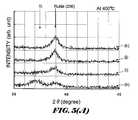
- FIGS. 3(A) and 3(B)are views showing analysis results on crystal structures of each manufactured sample with a XRD (X-ray diffraction) method, wherein FIG. 3(A) shows diffraction strength waveforms (vertical axis) with a horizontal axis (2 ⁇ ) when the incident angle ( ⁇ ) of X-ray on a sample surface is changed to 10-90 degrees and FIG. 3(B) shows an enlarged result of a range of 35-45 degrees of the horizontal axis (2 ⁇ );
- FIG. 4is a view showing a result of oxygen strength values of each manufactured sample with a XRF (X-ray fluorescence element analysis) method, wherein a horizontal axis indicates annealing temperatures and a vertical axis indicates inherent X-ray strengths of an oxygen element;
- XRFX-ray fluorescence element analysis
- FIGS. 5(A) and 5(B)are views illustrating a measurement results of the XRD method showing an effect of annealing time on annealing temperatures, wherein FIG. 5(A) is a measurement result at 400° C. and FIG. 5 (B) is a measurement result of 350° C.;
- FIG. 6shows a conceptual diagram showing a plan layout of a memory cell part of a DRAM device that is a semiconductor device according to an embodiment of the invention
- FIG. 7is a schematic sectional view taken along a line of A-A′ in FIG. 6 ;
- FIG. 8is a schematic sectional view illustrating a manufacturing process of a capacitor shown in FIG. 7 ;
- FIG. 9is a schematic sectional view illustrating a manufacturing process of a capacitor shown in FIG. 7 ;
- FIG. 10is a schematic sectional view illustrating a manufacturing process of a capacitor shown in FIG. 7 ;
- FIG. 11is a flow chart showing a manufacturing process of a capacitor using the invention.
- FIG. 12is a timing chart showing a method of supplying a plurality of gases in the manufacturing process of the capacitor shown in FIG. 11 .
- a TiO 2 film of a rutile crystal structureis formed in accordance with a process of two steps, as shown in FIG. 1 .
- a Ti (titanium) filmis deposited (step S 1 ).
- the Ti filmmay be deposited by a CVD method including an ALD method or sputtering method. That is, the invention is not particularly limited with respect to the method of forming the film.
- TiCl 4may be formed by using, as reaction gases, source gas and reduction gas such as H 2 , NH 3 or mixed gases of N 2 and NH 3 .
- source gas and reduction gassuch as H 2 , NH 3 or mixed gases of N 2 and NH 3 .
- the source gasis not particularly limited as long as precursor Ti and oxygen are not directly combined. Even in this case, since the source gas is not well reacted with the reduction gas at the low temperatures, it is necessary to increase the reactivity as described above.
- the deposited Tiis oxidized and thus converted into a TiO 2 film (step S 2 ).
- the above temperature rangeis just an example and the annealing temperature is not limited to the temperature range, as described below.
- the Ti filmis oxidized to form a TiO 2 film as described above, so that it is possible to form a TiO 2 film of a rutile crystal structure only with the heat treatment of low temperatures.
- a sample for evaluationwas manufactured as follows.
- a silicon oxide film 2was formed on a semiconductor substrate 1 and a Ti film was then formed thereon in a thickness of 20 nm.
- a sputtering methodwas used in which a substrate temperature was maintained at the temperature of 300° C., a chamber was maintained at the pressure of 0.5 Pa under Ar environment and a sputtering was performed to a Ti target under such state, thereby depositing a Ti film 3 on the silicon oxide film 2 .
- annealing oxidization(hereinafter, the annealing under oxygen environment is referred to as oxygen annealing) was performed and the Ti film 3 was thus oxidized to form a TiO 2 film 4 .
- oxygen annealingannealing oxidization
- a plurality of conditionswere set in a range of 300° C.-550° C. for evaluation and each oxygen annealing was performed for 10 minutes according to each temperature condition.
- the TiO 2 filmis formed on silicon, so that a silicon oxide film is always formed between the silicon and the TiO 2 film.
- a baseis not necessarily the silicon oxide.
- the inventionwhen the invention is applied to a capacitor that is used in a general semiconductor device, it is desirable to deposit a Ti film on a metal electrode and to perform the annealing under oxidative environment. Further, the material of the electrode is not particularly limited as long as it has a characteristic of oxidation resistance.
- FIGS. 3(A) and 3(B)show analysis results on crystal structures of each manufactured sample.
- FIG. 3(A)shows diffraction strength waveforms (vertical axis) with a horizontal axis (2 ⁇ ) when the incident angle ( ⁇ ) of X-ray on a sample surface is changed to 10-90 degrees.
- the waveform of (a)is a measurement result of the sample when the oxygen annealing was not performed and the waveforms of (b) to (g) are measurement results of the sample when the temperature condition of the oxygen annealing was increased to 300° C.-550° C. by 50° C.
- Each measured waveform of (a) to (g)is shifted in the direction of the vertical axis while using the common horizontal axis, so as to recognize positions of strength peaks.
- the positions of the strength peaksare indicated with arrows.
- a strength peak peculiar to TiO 2 of an anatase crystal structureis not seen in each waveform (a) to (g).
- the TiO 2 film formed by the method of this exemplary embodimentdoes not include an anatase crystal, including a case that the oxygen annealing was performed at the temperatures of 450° C. or more.
- FIG. 3(B)shows an enlarged result of a range of 35-45 degrees of the horizontal axis (2 ⁇ ).
- the corresponding strength peakindicates a-axis (200) peak of a rutile crystal of TiO 2 .
- FIG. 4a measurement result of oxygen strength values of each manufactured sample with an XRF (X-ray fluorescence element analysis) method is shown in FIG. 4 wherein a horizontal axis indicates annealing temperatures and a vertical axis indicates inherent X-ray intensity of an oxygen element.
- XRFX-ray fluorescence element analysis
- a point plotted in the leftmost of FIG. 4indicates a measurement result of the sample for which the oxygen annealing has not been performed. Even though the annealing has not been performed, the intensity is not 0 (zero) because the oxygen contained in the silicon oxide film 2 of the base is included in the measurement result. In other words, the intensity measured under state that the oxygen annealing has not been performed becomes a starting-point intensity.
- the oxygen annealingWhen the oxygen annealing is performed, the number of atoms is increased as the annealing temperature is increased. The intensity is almost saturated around 450° C. at which the Ti peak disappears in the XRD method. This matches an aspect in which the oxidization of Ti is developed. In this exemplary embodiment, it is possible to form a TiO 2 film of a rutile structure even at the low temperatures of 400° C. by prolonging the oxygen annealing time.
- a sample on which a Ti film was deposited as described abovewas prepared.
- a resultwill be described which was obtained when the oxygen annealing time was changed while the temperature of the oxygen annealing was fixed.
- FIG. 5(A)is a measurement result of the XRD method when the temperature of the oxygen annealing was set at 400° C. and the oxygen annealing time was increased to 10-40 minutes by 10 minutes.
- Each waveform of (h) to (k)corresponds to each case where the oxygen annealing time was increased by 10 minutes.
- FIG. 5(B)is a measurement result of the XRD method when the temperature of the oxygen annealing was set at 350° C. and the oxygen annealing time was increased to 10-40 minutes by 10 minutes.
- each waveform of (h) to (k)corresponds to each case where the oxygen annealing time was increased by 10 minutes.
- the thickness of the Ti filmwas thinner, it was possible to form the TiO 2 film of the rutile crystal structure even with the oxygen annealing at 350° C. That is, in this exemplary embodiment, it is desirable to continue the oxidization until the Ti film is oxidized to completely change into TiO 2 film and to set the oxidization time in accordance with the film thickness of Ti and the temperature of the oxygen annealing.
- the manufacturing method of this exemplary embodimentis very effective.
- the reason to form a TiO 2 film of a rutile crystal structure by using the manufacturing method of this exemplary embodimentis as follows:
- the anatase crystallizationis started at the temperature range of 250-300° C., so that the anatase crystal is made.
- the transformation into the rutile crystalis difficult.
- the Ti filmwhen the Ti film is deposited from the beginning, the Ti film is still maintained under metal state at the temperature range of 250-300° C. and the oxidization is barely started at the temperatures of 300° C. or more ( FIG. 4 ). Due to this, the Ti metal film, as it is, can pass to the temperature ranges at which the anatase crystallization is started, so that it is possible to avoid the anatase crystallization and thus to make the rutile crystal.
- the Ti film to be originally formedis crystallized under deposited state. This is because it is possible to easily diffuse the oxygen and to easily oxidize the whole film under crystalline state rather than amorphous state.
- the annealing temperatureis 400° C. or less under oxidative environment.
- the temperatureis not particularly limited to 350° C. or more. In other words, it may be possible to perform the oxidization treatment at the temperatures of 350° C. or less as long as the deposited Ti film is oxidized to change into a rutile-type TiO 2 film.
- the environmentis not particularly limited to the oxygen gas (O 2 gas). That is, any environment is possible as long as it is an oxidative environment including the oxygen atoms.
- O 2 gasoxygen gas
- ozone (O 3 ) gas, steam (H 2 O), nitrous oxide (NO) gas and the likecan be used.
- the oxidative gassuch as ozone, steam and the like because the oxidative gas can reduce the oxidization time.
- FIG. 6shows a conceptual diagram showing a plan layout of a memory cell part of a DRAM device that is a semiconductor device to which the invention is applied.
- the right side of FIG. 6is shown with a perspective sectional view based on a plane that cuts a gate electrode 5 and a side wall 5 b that will be a word wiring (W), which will be described below.
- Wword wiring
- a capacitoris not shown in FIG. 6 and is shown with a sectional view only.
- FIG. 7is a schematic sectional view taken along a line of A-A′ of the memory cell part ( FIG. 6 ). Meanwhile, the drawings are provided only to illustrate a structure of a semiconductor device and it should be understood that the dimensions or sizes of each part shown are different from those of an actual semiconductor device.
- the memory cell partis schematically constituted by MOS transistors (Tr 1 ) and capacitors (Cap) connected to the MOS transistors through a plurality of contact plugs.
- a semiconductor substrate 101is made of silicon (Si) containing p-type impurities of a predetermined concentration.
- the semiconductor substrate 101is formed with element isolation regions 103 .
- the element isolation region 103are formed at parts except active regions (K) by embedding an insulating film such as silicon oxide film (SiO 2 ) in a surface of the semiconductor substrate 101 by a STI (Shallow Trench Isolation) method and are insulation-isolated from the neighboring active regions (K).
- STISilicon Trench Isolation
- a plurality of active regions (K) having a thin and long rectangular shapeare aligned to be inclined in a right downward direction at a predetermined interval and arranged in accordance with a layout referred to as a 6F 2 -type memory cell.
- Both ends and a central part of each active region (K)are formed with impurity diffusion layers, respectively, which function as source/drain regions of the MOS transistor (Tr 1 ).
- Positions of substrate contact parts 205 a , 205 b , 205 care defined so that they are arranged just above the source/drain regions (impurity diffusion layers).
- bit wirings 106 of a broken line shapeare extended in a horizontal (X) direction.
- the bit wirings 106are arranged at an interval in the vertical (Y) direction of FIG. 6 .
- word wirings W of a straight line shapeare arranged which are extended in the vertical (Y) direction of FIG. 6 .
- Each of the word wirings Wis arranged at a predetermined interval in the horizontal (X) direction of FIG. 6 .
- the word wiring Wis structured to include a gate electrode 105 shown in FIG. 7 in a part at which the word wiring W intersects the active region K.
- the MOS transistor Tr 1has a gate electrode of a recess shape.
- impurity diffusion layers 108 functioning as source/drain regionsare spaced and formed in the active regions K sectioned in the element isolation regions 103 of the semiconductor substrate 101 and the gate electrodes 105 of a recess shape are formed between the impurity diffusion layers 108 .
- the gate electrode 105is formed to protrude above an upper part of the semiconductor substrate 101 by a multi-layered film of a polycrystalline silicon film and a metal film.
- the polycrystalline silicon filmmay be formed by including an impurity such as phosphorous when forming a film through a CVD method.
- metal film for the gate electrodemetal having a high melting point such as tungsten (W), tungsten nitride (WN), tungsten silicide (WSi) and the like may be used.
- gate insulating films 105 aare formed between the gate electrodes 105 and the semiconductor substrate 101 .
- sides of the gate electrode 105are formed with sidewalls 105 h h an insulating film such as silicon nitride (Si 3 N 4 ) and the like.
- An upper surface of the gate electrode 105is also formed with an insulating film 105 c of silicon nitride, for example, so that the insulating film protects the upper surface.
- the impurity diffusion layer 108is formed by introducing phosphorous, for example, as a n-type impurity, into the semiconductor substrate 101 .
- Substrate contact plugs 109are formed to contact the impurity diffusion layers 108 .
- the substrate contact plugs 109are respectively arranged at the positions 205 c , 205 b , 205 c of the substrate contact parts shown in FIG. 6 , and are formed polycrystalline silicon containing phosphorous, for example.
- a horizontal (X) width of the substrate contact plug 109is formed into a self-aligned structure shape in which the width is defined by the sidewalls 105 b provided to the neighboring gate wirings W.
- a first interlayer insulating film 104is formed to cover the insulating films 105 c on the gate electrodes and the substrate contact plugs 109 and a bit line contact plug 104 A is formed to pass through the first interlayer insulating film 104 .
- the bit line contact plug 104 Ais located at the position of the substrate contact part 205 a and is conductively connected to the substrate contact plug 109 .
- the bit line contact plug 104 Ais formed by depositing tungsten (W) and the like on a barrier film (TiN/Ti) consisting of a stacked film of titanium (Ti) and titanium nitride (TiN).
- the bit wiring 106is formed to connect with the bit line contact plug 104 A.
- the bit wiring 106is made of a stacked film consisting of tungsten nitride (WN) and tungsten (W).
- a second interlayer insulating film 107is formed to cover the bit wiring 106 .
- Capacitor contact plugs 107 Aare formed to pass through the first interlayer insulating film 104 and the second interlayer insulating film 107 and to connect with the substrate contact plugs 109 .
- the capacitor contact plugs 107 Aare arranged at the positions of the substrate contact parts 205 b , 205 c.
- a third interlayer insulating film 111 made of silicon nitride and a fourth interlayer insulating film 112 made of silicon oxideare formed above the second interlayer insulating film 107 .
- Capacitorsare formed to pass through the third interlayer insulating film 111 and the fourth interlayer insulating film 112 and to connect with the capacitor contact plugs 107 A.
- the capacitor (Cap)is structured in such a manner that the TiO 2 film formed by the invention is sandwiched between a lower electrode 113 and an upper electrode 115 and the lower electrode 113 is conductively connected to the capacitor contact plug 107 A.
- a fifth interlayer insulating film 120 made of silicon oxide and the like, an upper wiring layer 121 made of aluminum (Al), copper (Cu) and the like and a surface protecting film 122are formed above the upper electrode 115 .
- the upper electrode 115 of the capacitoris provided with a predetermined potential, so that it functions as a DRAM device performing an information storing operation by determining whether or not charges kept in the capacitor.
- FIGS. 8 to 10are sectional views showing only upper parts from the third interlayer insulating film 111 .
- the third interlayer insulating film 111 and the fourth interlayer insulating film 112are deposited to have a predetermined film thickness. Then, opening holes 112 A for forming capacitors are formed with a photolithography technique.
- the lower electrode 113is formed with dry etching or CMP (Chemical Mechanical Polishing) technique so that it remains only inner walls of the opening holes 112 A.
- CMPChemical Mechanical Polishing
- the material of the lower electrodeit is preferable to use a metal film having strong oxidization resistance.
- ruthenium (Ru), iridium (Ir), platinum (Pt) and the likemay be exemplified.
- a Ti film 114 ais deposited to have a thickness of 10 nm or less, for example about 6-8 nm.
- the method of depositing the Ti filmis not particularly limited. However, it is preferable to use an ALD method when depositing a Ti film of a uniform thickness in a deep hole, like a capacitor of a DRAM device.
- the Ti film 114 ais converted into a TiO 2 film 114 .
- the third interlayer insulating film 111with silicon nitride having less oxygen penetration property than silicon oxide for a typical interlayer insulating film, it is possible to prevent the bit line or transistor located below the capacitor from being damaged due to the oxidization.
- the temperature and time of the oxygen annealingmay be adjusted so that the Ti film can be completely oxidized, correspondingly to a thickness of a TiO 2 film to be desired.
- the oxygen environmentdoes not necessarily require 100% oxygen. In other words, a mixed environment of inactive gas and oxygen, for example the ambient air may be possible. The environment in which oxygen is sufficient is preferable.
- a metal filmis deposited to cover the surface of the TiO 2 film 114 and to fill the opening holes 112 A, thereby forming the upper electrode 115 .
- the material of the upper electrode 115may be different from that of the lower electrode 113 .
- tungsten (W) or titanium nitride (TiN) and the like having weak oxidization resistancemay be used.
- the capacitors (Cap)are completed.
- the TiO 2 film of a rutile crystal structurehaving a high dielectric constant at the low temperatures of 400° C. or less.
- FIG. 11is a flow chart showing a process of forming a capacitor.
- a lower electrode of a capacitoris formed on a semiconductor substrate.
- ruthenium (Ru), iridium (Ir), platinum (Pt) and the likemay be used as the material of the lower electrode.
- the other metal film having strong oxidization resistancemay be used.
- the semiconductor substrate having the lower electrode formed thereonis set in a chamber of the ALD apparatus.
- the ALD apparatus of a sheet type or batch typemay be used.
- a TiO 2 filmis formed in the ALD apparatus through the step S 4 of depositing a Ti film and the step S 5 of oxidizing the deposited Ti film to convert into a TiO 2 film of a rutile crystal structure.
- the step S 4 of depositing a Ti filmcomprises the step S 4 a of supplying Ti source gas (precursor) and the step S 4 b of supplying reduction gas.
- FIG. 12is a timing chart of a plurality of gases to be supplied to the ALD apparatus.
- the temperature of the semiconductor substrate in the chamberis set at 400° C.
- TiCl 4may be exemplified.
- the Ti source gasis not particularly limited as long as Ti and oxygen are not directly combined.
- the Ti source gasis supplied into the chamber for 1-5 seconds at time T 1 and adsorbed into the surface of the lower electrode. Then, at time T 2 , the supply of the Ti source gas is stopped and the purging gas is supplied into the chamber for 5-30 seconds.
- the purging gasnitrogen (N 2 ) may be exemplified.
- the supply of the purging gasis stopped and the reduction gas is supplied into the chamber for 2-5 seconds in the step S 4 b .
- the reduction gashydrogen (H 2 ) may be exemplified.
- the reduction gasis activated through a plasma generator provided in the ALD apparatus so as to accelerate the reaction with the Ti source adsorbed.
- FIG. 12shows two cycles (time T 5 -T 9 ) as the step S 4 .
- the oxidizing gasis supplied into the chamber for 1-2 minutes in the step S 5 .
- the oxidizing gasozone (O 3 ) may be used.
- the Ti filmis completely oxidized and converted into a rutile-type TiO 2 film.
- the TiO 2 film having a thickness of about 3.4 nmwas obtained by the oxidization.
- M timesM: positive integer
- the substrateis maintained at the temperatures higher than that of the prior art and the reduction gas is supplied just after supplying the Ti source gas, so that a crystalline Ti film of a level of an atomic layer is formed. Then, by repeating the process of forming the Ti film of a level of an atomic level, the crystalline Ti film is made to have a predetermined thickness and then the oxidizing gas is supplied to oxidize the Ti film, so that a TiO 2 film of a rutile crystal structure is obtained.
- the material of the upper electrodemay be different from that of the lower electrode.
Landscapes
- Engineering & Computer Science (AREA)
- Power Engineering (AREA)
- Microelectronics & Electronic Packaging (AREA)
- Manufacturing & Machinery (AREA)
- Chemical & Material Sciences (AREA)
- Inorganic Chemistry (AREA)
- Ceramic Engineering (AREA)
- Computer Hardware Design (AREA)
- General Physics & Mathematics (AREA)
- Condensed Matter Physics & Semiconductors (AREA)
- Physics & Mathematics (AREA)
- Semiconductor Memories (AREA)
- Formation Of Insulating Films (AREA)
Abstract
Description
This application is based on Japanese Patent applications Nos. 2009-088951 and 2010-009000, the contents of which are incorporated hereinto by reference.
1. Field of the Invention
The present invention relates to a method of manufacturing a capacitive insulating film for a capacitor, and more particularly, to a method of forming a TiO2film having a rutile crystal structure at low temperatures of 400° C. or less.
2. Description of the Related Art
As a semiconductor device such as DRAM device is finer, an insulating film for a capacitor having a high dielectric constant (capacitive insulating film) is needed.
As insulating material for a capacitor having a high dielectric constant, TiO2(titanium oxide) may be exemplified. There are two types of crystal structures, i.e., anatase and rutile types in TiO2, which are well-known. The anatase crystal is a low temperature phase that is apt to be formed at low temperatures and has a low relative dielectric constant of about 40 or less. In the meantime, the rutile crystal is a high temperature phase that is typically formed at high temperatures and has a high relative dielectric constant of about 80 or more. In particular, when the rutile crystal is used as insulating material for a capacitor, it is possible to manufacture a high-capacity capacitor.
A TiO2film can be formed by a variety of methods such as CVD (Chemical Vapor Deposition), ALD (Atomic Layer Deposition) and the like. When the TiO2film is used for a semiconductor device, the ALD method is mainly used due to a standpoint of fining. However, when forming the TiO2film to be used for a semiconductor device, it is difficult to form a rutile crystal of a high dielectric constant at low temperatures of 400° C. or less even with any method including the ALD method.
For example, according to the experiments performed by Gyeong Teak Lim et al. (Thin Solid Films 498 (2006) p 254-258), a TiO2film is formed on silicon with the ALD method using precursor of TDMAT (tetrakis-(dimethylamino)titanium) and oxidizer of H2O. The TiO2film becomes amorphous just after forming the film and is then crystallized by performing the annealing. The anatase crystals are generated with the annealing of 300° C. or more, the rutile and anatase crystals are generated at 700° C. or more and the rutile crystals become main at 800° C. or more. However, in a semiconductor process, it is difficult to perform the annealing at high temperatures, so as to avoid a bad effect on a semiconductor device such as transistor, as the device is gradually finer. Thus, it is actually impossible to perform the annealing at the high temperatures for obtaining the rutile crystals.
In addition, JP-A 2000-254519 discloses a technology of illuminating Ar ion beam so as to form a stacked structure of a rutile-type TiO2film and an anatase-type TiO2film for photocatalyst, thereby lowering a structure transition temperature from the anatase-type structure to the rutile-type structure. However, even with such means, the annealing of 500° C. or more should be performed so as to obtain a TiO2film of the rutile crystal structure. In addition, when forming the TiO2film in a location having a three-dimensional structure, such as a capacitor of a DRAM device, it is difficult to uniformly introduce the Ar ions by the ion illumination.
Additionally, JP-A 2007-110111 discloses a technology of forming a RuO2film on a surface of a lower electrode for a capacitor, which electrode is made of Ru (ruthenium), thereby obtaining the rutile-type TiO2film at low temperatures of 400° C. or less. However, since the material of the lower electrode is limited to Ru, it is difficult to change the material of the electrode and thus to form a capacitor having higher performance.
Thus, the inventors studied a method capable of forming a TiO2film of a rutile crystal structure at temperatures as low as possible and easily forming a uniform TiO2film without undergoing influences of electrode shapes and materials of a base even when it is applied to a capacitor of a three dimensional structure.
The inventors carried out an experiment of forming a TiO2film using the ALD method. However, the anatase crystals were apt to be formed in a method of directly forming a TiO2film. In addition, even when studying the annealing method, it was difficult to obtain a TiO2film having rutile crystals only.
To be more specific, the TiO2film formed at 200° C. was amorphous. When the amorphous film was crystallized with the annealing of high temperatures, both the anatase crystals and the rutile crystals were mixed. In addition, when the TiO2film was formed at 250° C. or more, the anatase crystals were generated from the beginning. The anatase crystals once formed were stable and were not extinguished even when performing the annealing treatment of high temperatures at which the rutile crystals are generated. The anatase crystals are not desirable because they lower the dielectric constant.
The present invention has been made to solve the above problems occurring in the prior art. The invention provides a method of easily forming a TiO2film having a rutile crystal structure at relatively low temperatures. The means provided by the invention is to deposit a Ti film and to oxidize the Ti film with an annealing treatment under oxidative environment, thereby converting the Ti film into a TiO2film having a rutile crystal structure.
Specifically, according to an embodiment of the invention, there is provided a method of manufacturing a capacitive insulating film for a capacitor. The method comprises:
depositing a Ti film, and
annealing the Ti film under oxidative environment, thereby converting the Ti film into a TiO2film having a rutile crystal structure.
In addition, according to another embodiment of the invention, there is provided a method of manufacturing a semiconductor device having a capacitor. The method comprises:
forming a lower electrode of a capacitor,
depositing a Ti film on the lower electrode,
annealing the Ti film under oxidative environment, thereby converting the Ti film into a TiO2film having a rutile crystal structure, and
forming an upper electrode of the capacitor on the TiO2film.
It is possible to form a TiO2film of a rutile crystal structure having a high dielectric constant at low temperatures of 350-400° C., as a capacitive insulating film for a capacitor. As a result, it is possible to increase the capacitance of a capacitor and to avoid a bad influence of the high temperature heat treatment on a semiconductor element such as a transistor, so that it is possible to provide a fined semiconductor device of high performance.
The above features and advantages of the present invention will be more apparent from the following description of certain preferred embodiments taken in conjunction with the accompanying drawings, in which:
The invention will be now described herein with reference to illustrative embodiments. Those skilled in the art will recognize that many alternative embodiments can be accomplished using the teachings of the present invention and that the invention is not limited to the embodiments illustrated for explanatory purpose.
{Exemplary Embodiments}
In the followings, a method of manufacturing a TiO2film according to an exemplary embodiment of the invention will be described.
In this exemplary embodiment, a TiO2film of a rutile crystal structure is formed in accordance with a process of two steps, as shown inFIG. 1 .
After forming a lower electrode for a capacitor, a Ti (titanium) film is deposited (step S1). The Ti film may be deposited by a CVD method including an ALD method or sputtering method. That is, the invention is not particularly limited with respect to the method of forming the film.
When the Ti film is formed by the CVD method (or ALD method), TiCl4, for example, may be formed by using, as reaction gases, source gas and reduction gas such as H2, NH3or mixed gases of N2and NH3. In the meantime, it is difficult to react the source gas at low temperatures and it is thus necessary to increase reactivity by plasmic reaction gases, for example. The source gas is not particularly limited as long as precursor Ti and oxygen are not directly combined. Even in this case, since the source gas is not well reacted with the reduction gas at the low temperatures, it is necessary to increase the reactivity as described above.
Next, by performing the annealing treatment under oxidative environment at temperatures of about 350-400° C., the deposited Ti is oxidized and thus converted into a TiO2film (step S2). The above temperature range is just an example and the annealing temperature is not limited to the temperature range, as described below.
Contrary to the prior art of depositing a TiO2film from the beginning, the Ti film is oxidized to form a TiO2film as described above, so that it is possible to form a TiO2film of a rutile crystal structure only with the heat treatment of low temperatures.
A crystal state of the TiO2film formed by the method of this exemplary embodiment will be described.
A sample for evaluation was manufactured as follows.
First, as shown in (a) ofFIG. 2 , asilicon oxide film 2 was formed on asemiconductor substrate 1 and a Ti film was then formed thereon in a thickness of 20 nm. To be more specific, a sputtering method was used in which a substrate temperature was maintained at the temperature of 300° C., a chamber was maintained at the pressure of 0.5 Pa under Ar environment and a sputtering was performed to a Ti target under such state, thereby depositing aTi film 3 on thesilicon oxide film 2.
Subsequently, as shown in (b) ofFIG. 2 , by furnace annealing using a heat treatment furnace that supplies oxygen gas, annealing oxidization (hereinafter, the annealing under oxygen environment is referred to as oxygen annealing) was performed and theTi film 3 was thus oxidized to form a TiO2film4. Regarding the temperatures of the oxygen annealing, a plurality of conditions were set in a range of 300° C.-550° C. for evaluation and each oxygen annealing was performed for 10 minutes according to each temperature condition.
In the meantime, in the prior art (Gyeong Teak Lim et al.), the TiO2film is formed on silicon, so that a silicon oxide film is always formed between the silicon and the TiO2film. Thus, in order to compare the characteristics of the film at the same conditions, the TiO2film was formed on the silicon oxide. In the invention, a base is not necessarily the silicon oxide. In addition, when the invention is applied to a capacitor that is used in a general semiconductor device, it is desirable to deposit a Ti film on a metal electrode and to perform the annealing under oxidative environment. Further, the material of the electrode is not particularly limited as long as it has a characteristic of oxidation resistance.
In the state (a) that the oxygen annealing was not performed, a crystal peak of Ti is seen around 2θ=38°. As the temperature of the oxygen annealing is increased, the Ti peak strength is decreased and shifted in a left direction. This indicates that a lattice interval of the Ti crystal is widened because a part of the Ti crystal is oxidized to collapse the crystal structure and the oxygen is introduced into the Ti crystal. The Ti crystal exists up to the oxygen annealing (d) of 400° C. and is completely extinguished in the oxygen annealing (e) of 450° C.
Instead, a new peak appears around 2θ=39° for the oxygen annealing of 400° C. or more. The corresponding strength peak indicates a-axis (200) peak of a rutile crystal of TiO2. As the annealing temperature is increased, the peak is gradually stronger, is shifted in a right direction and approaches a position (2θ=39.2 degree) of TiO2bulk crystal of the rutile structure.
In the followings, a measurement result of oxygen strength values of each manufactured sample with an XRF (X-ray fluorescence element analysis) method is shown inFIG. 4 wherein a horizontal axis indicates annealing temperatures and a vertical axis indicates inherent X-ray intensity of an oxygen element.
By the XRF method, it is possible to obtain peak intensity proportional to the number of atoms in a target element. A point plotted in the leftmost ofFIG. 4 indicates a measurement result of the sample for which the oxygen annealing has not been performed. Even though the annealing has not been performed, the intensity is not 0 (zero) because the oxygen contained in thesilicon oxide film 2 of the base is included in the measurement result. In other words, the intensity measured under state that the oxygen annealing has not been performed becomes a starting-point intensity.
When the oxygen annealing is performed, the number of atoms is increased as the annealing temperature is increased. The intensity is almost saturated around 450° C. at which the Ti peak disappears in the XRD method. This matches an aspect in which the oxidization of Ti is developed. In this exemplary embodiment, it is possible to form a TiO2film of a rutile structure even at the low temperatures of 400° C. by prolonging the oxygen annealing time.
A sample on which a Ti film was deposited as described above was prepared. In the followings, a result will be described which was obtained when the oxygen annealing time was changed while the temperature of the oxygen annealing was fixed.
As can be seen fromFIG. 5(A) , when the oxygen annealing was performed at 400° C., the Ti peak gradually disappeared and the peak of the rutile crystal was increased as the oxygen annealing time was increased. When the oxygen annealing was performed for 40 minutes, the Ti peak almost disappeared and the intensity of the rutile peak was sufficient (waveform (k)).
In addition, as can be seen from the result ofFIG. 5(B) , when the oxygen annealing was performed at 350° C., the Ti peak quite remained even after the oxygen annealing was performed for 40 minutes. However, some rutile peak was seen (waveform (k)). The reason is as follows: since the Ti film thickness of the prepared sample was thick, i.e., 20 nm, the Ti peak remained until all Ti was oxidized. Since the oxidization is developed from a surface of the Ti film, a part near the lower electrode has not been oxidized yet.
According to a further study, when the thickness of the Ti film was thinner, it was possible to form the TiO2film of the rutile crystal structure even with the oxygen annealing at 350° C. That is, in this exemplary embodiment, it is desirable to continue the oxidization until the Ti film is oxidized to completely change into TiO2film and to set the oxidization time in accordance with the film thickness of Ti and the temperature of the oxygen annealing.
For example, for a case where the invention is applied to a fine memory cell having a minimum processing size of 60 nm or less, it is necessary to make a film thickness of a capacitive insulatingfilm 10 nm or less. Thus, the manufacturing method of this exemplary embodiment is very effective.
Like this, by using the manufacturing method of this exemplary embodiment, it is possible to manufacture a TiO2film having a rutile crystal only, i.e., having no anatase crystal at the low temperatures of 350° C.-400° C.
The reason to form a TiO2film of a rutile crystal structure by using the manufacturing method of this exemplary embodiment is as follows:
When Ti atoms and oxygen atoms are originally combined to form a TiO2film as the prior art, the anatase crystallization is started at the temperature range of 250-300° C., so that the anatase crystal is made. In addition, when the anatase crystal is once formed, the transformation into the rutile crystal is difficult.
However, when the Ti film is deposited from the beginning, the Ti film is still maintained under metal state at the temperature range of 250-300° C. and the oxidization is barely started at the temperatures of 300° C. or more (FIG. 4 ). Due to this, the Ti metal film, as it is, can pass to the temperature ranges at which the anatase crystallization is started, so that it is possible to avoid the anatase crystallization and thus to make the rutile crystal.
In the meantime, it is preferable that the Ti film to be originally formed is crystallized under deposited state. This is because it is possible to easily diffuse the oxygen and to easily oxidize the whole film under crystalline state rather than amorphous state. Thus, when depositing a Ti film, it is preferable to form the film at the temperatures (about 200-400° C.) as high as possible.
In addition, when forming a capacitor for a semiconductor device, it is preferable to form the capacitor at the temperatures as low as possible. Thus, it is preferable that the annealing temperature is 400° C. or less under oxidative environment. When forming a TiO2film under state in which the effect of heat is not particularly considered, it may be possible to perform the annealing at the temperatures above 400° C. Accordingly, it is possible to set the annealing temperature in accordance with the characteristics required for a semiconductor device to be manufactured.
Meanwhile, when performing the oxygen annealing under oxygen gas environment, it is preferable to perform the annealing at the temperatures of 350° C. or more, as described above. However, when using another oxidization method, the temperature is not particularly limited to 350° C. or more. In other words, it may be possible to perform the oxidization treatment at the temperatures of 350° C. or less as long as the deposited Ti film is oxidized to change into a rutile-type TiO2film.
In addition, when performing the annealing, the environment is not particularly limited to the oxygen gas (O2gas). That is, any environment is possible as long as it is an oxidative environment including the oxygen atoms. To be more specific, ozone (O3) gas, steam (H2O), nitrous oxide (NO) gas and the like can be used. In particular, when performing the oxidization at low temperatures, it is preferable to use the oxidative gas such as ozone, steam and the like because the oxidative gas can reduce the oxidization time.
In the followings, it will be described a case where the invention is applied to a capacitive insulating film of a capacitor (capacitive device) constituting a memory cell of a DRAM device, which is a specific example to which the invention is applied.
As shown inFIG. 7 , the memory cell part is schematically constituted by MOS transistors (Tr1) and capacitors (Cap) connected to the MOS transistors through a plurality of contact plugs.
InFIGS. 6 and 7 , asemiconductor substrate 101 is made of silicon (Si) containing p-type impurities of a predetermined concentration. Thesemiconductor substrate 101 is formed withelement isolation regions 103. Theelement isolation region 103 are formed at parts except active regions (K) by embedding an insulating film such as silicon oxide film (SiO2) in a surface of thesemiconductor substrate 101 by a STI (Shallow Trench Isolation) method and are insulation-isolated from the neighboring active regions (K). In this exemplary embodiment, it is shown a case where the invention is applied to a cell structure in which a memory cell of 2 bits is arranged in one active region (K).
In this exemplary embodiment, as the plan structure shown inFIG. 6 , a plurality of active regions (K) having a thin and long rectangular shape are aligned to be inclined in a right downward direction at a predetermined interval and arranged in accordance with a layout referred to as a 6F2-type memory cell.
Both ends and a central part of each active region (K) are formed with impurity diffusion layers, respectively, which function as source/drain regions of the MOS transistor (Tr1). Positions ofsubstrate contact parts
InFIG. 6 , bit wirings106 of a broken line shape (bent shape) are extended in a horizontal (X) direction. The bit wirings106 are arranged at an interval in the vertical (Y) direction ofFIG. 6 . In addition, word wirings W of a straight line shape are arranged which are extended in the vertical (Y) direction ofFIG. 6 . Each of the word wirings W is arranged at a predetermined interval in the horizontal (X) direction ofFIG. 6 . The word wiring W is structured to include agate electrode 105 shown inFIG. 7 in a part at which the word wiring W intersects the active region K. In this exemplary embodiment, the MOS transistor Tr1 has a gate electrode of a recess shape.
As shown in the sectional structure ofFIG. 7 , impurity diffusion layers108 functioning as source/drain regions are spaced and formed in the active regions K sectioned in theelement isolation regions 103 of thesemiconductor substrate 101 and thegate electrodes 105 of a recess shape are formed between the impurity diffusion layers108.
Thegate electrode 105 is formed to protrude above an upper part of thesemiconductor substrate 101 by a multi-layered film of a polycrystalline silicon film and a metal film. The polycrystalline silicon film may be formed by including an impurity such as phosphorous when forming a film through a CVD method. As the metal film for the gate electrode, metal having a high melting point such as tungsten (W), tungsten nitride (WN), tungsten silicide (WSi) and the like may be used.
In addition, as shown inFIG. 7 ,gate insulating films 105aare formed between thegate electrodes 105 and thesemiconductor substrate 101. In addition, sides of thegate electrode 105 are formed with sidewalls105hh an insulating film such as silicon nitride (Si3N4) and the like. An upper surface of thegate electrode 105 is also formed with an insulatingfilm 105cof silicon nitride, for example, so that the insulating film protects the upper surface.
Theimpurity diffusion layer 108 is formed by introducing phosphorous, for example, as a n-type impurity, into thesemiconductor substrate 101. Substrate contact plugs109 are formed to contact the impurity diffusion layers108. The substrate contact plugs109 are respectively arranged at thepositions FIG. 6 , and are formed polycrystalline silicon containing phosphorous, for example. A horizontal (X) width of thesubstrate contact plug 109 is formed into a self-aligned structure shape in which the width is defined by thesidewalls 105bprovided to the neighboring gate wirings W.
As shown inFIG. 7 , a firstinterlayer insulating film 104 is formed to cover the insulatingfilms 105con the gate electrodes and the substrate contact plugs109 and a bitline contact plug 104A is formed to pass through the firstinterlayer insulating film 104. The bitline contact plug 104A is located at the position of thesubstrate contact part 205aand is conductively connected to thesubstrate contact plug 109. The bitline contact plug 104A is formed by depositing tungsten (W) and the like on a barrier film (TiN/Ti) consisting of a stacked film of titanium (Ti) and titanium nitride (TiN). Thebit wiring 106 is formed to connect with the bitline contact plug 104A. Thebit wiring 106 is made of a stacked film consisting of tungsten nitride (WN) and tungsten (W).
A secondinterlayer insulating film 107 is formed to cover thebit wiring 106. Capacitor contact plugs107A are formed to pass through the firstinterlayer insulating film 104 and the secondinterlayer insulating film 107 and to connect with the substrate contact plugs109. The capacitor contact plugs107A are arranged at the positions of thesubstrate contact parts
A thirdinterlayer insulating film 111 made of silicon nitride and a fourthinterlayer insulating film 112 made of silicon oxide are formed above the secondinterlayer insulating film 107.
Capacitors (Cap) are formed to pass through the thirdinterlayer insulating film 111 and the fourthinterlayer insulating film 112 and to connect with the capacitor contact plugs107A.
The capacitor (Cap) is structured in such a manner that the TiO2film formed by the invention is sandwiched between alower electrode 113 and anupper electrode 115 and thelower electrode 113 is conductively connected to thecapacitor contact plug 107A.
A fifthinterlayer insulating film 120 made of silicon oxide and the like, anupper wiring layer 121 made of aluminum (Al), copper (Cu) and the like and asurface protecting film 122 are formed above theupper electrode 115.
Theupper electrode 115 of the capacitor is provided with a predetermined potential, so that it functions as a DRAM device performing an information storing operation by determining whether or not charges kept in the capacitor.
In the followings, a method of forming the capacitor (Cap) will be specifically described.
First, as shown inFIG. 8 , the thirdinterlayer insulating film 111 and the fourthinterlayer insulating film 112 are deposited to have a predetermined film thickness. Then, opening holes112A for forming capacitors are formed with a photolithography technique.
After forming a film of lower electrode material, thelower electrode 113 is formed with dry etching or CMP (Chemical Mechanical Polishing) technique so that it remains only inner walls of the opening holes112A.
As the material of the lower electrode, it is preferable to use a metal film having strong oxidization resistance. Specifically, ruthenium (Ru), iridium (Ir), platinum (Pt) and the like may be exemplified.
Subsequently, as shown inFIG. 9 , a Ti film114ais deposited to have a thickness of 10 nm or less, for example about 6-8 nm. In the invention, the method of depositing the Ti film is not particularly limited. However, it is preferable to use an ALD method when depositing a Ti film of a uniform thickness in a deep hole, like a capacitor of a DRAM device.
Then, by performing the oxygen annealing at 400° C. for 30 minutes under oxygen environment, the Ti film114ais converted into a TiO2film114. At this time, by forming the thirdinterlayer insulating film 111 with silicon nitride having less oxygen penetration property than silicon oxide for a typical interlayer insulating film, it is possible to prevent the bit line or transistor located below the capacitor from being damaged due to the oxidization.
In addition, the temperature and time of the oxygen annealing may be adjusted so that the Ti film can be completely oxidized, correspondingly to a thickness of a TiO2film to be desired. The oxygen environment does not necessarily require 100% oxygen. In other words, a mixed environment of inactive gas and oxygen, for example the ambient air may be possible. The environment in which oxygen is sufficient is preferable.
Subsequently, as shown inFIG. 10 , a metal film is deposited to cover the surface of the TiO2film114 and to fill the opening holes112A, thereby forming theupper electrode 115. The material of theupper electrode 115 may be different from that of thelower electrode 113. In addition, tungsten (W) or titanium nitride (TiN) and the like having weak oxidization resistance may be used. Thus, the capacitors (Cap) are completed.
By applying the invention, it is possible to form the TiO2film of a rutile crystal structure having a high dielectric constant at the low temperatures of 400° C. or less.
Accordingly, it is possible to suppress the influence of heat to be applied to a semiconductor element such as transistor that is earlier formed than a capacitor, so that it is possible to form a finer transistor of high performance.
In addition, it is possible to easily form a TiO2film having a uniform thickness independent from a shape or material of the lower electrode and to increase the capacitance of a capacitor, so that it is possible to easily form a DRAM device of high performance.
In the followings, as an alternative method of manufacturing a capacitor having a TiO2film using the invention, it will be described a method of continuously implementing the process of depositing a Ti film and the annealing process under oxidative environment in one ALD film forming apparatus.
First, in a step S3, a lower electrode of a capacitor is formed on a semiconductor substrate. As the material of the lower electrode, ruthenium (Ru), iridium (Ir), platinum (Pt) and the like may be used. However, the other metal film having strong oxidization resistance may be used.
Subsequently, the semiconductor substrate having the lower electrode formed thereon is set in a chamber of the ALD apparatus. The ALD apparatus of a sheet type or batch type may be used.
A TiO2film is formed in the ALD apparatus through the step S4 of depositing a Ti film and the step S5 of oxidizing the deposited Ti film to convert into a TiO2film of a rutile crystal structure.
The step S4 of depositing a Ti film comprises the step S4aof supplying Ti source gas (precursor) and the step S4bof supplying reduction gas.
In this exemplary embodiment, four types of gases, i.e., Ti source gas, reduction gas, purging gas and oxidizing gas are supplied into the chamber in accordance with the timing shown inFIG. 12 .
The steps S4 and S5 will be described with reference toFIG. 12 .
The temperature of the semiconductor substrate in the chamber is set at 400° C.
As the Ti source gas, TiCl4may be exemplified. In addition, the Ti source gas is not particularly limited as long as Ti and oxygen are not directly combined.
First, in the step S4, the Ti source gas is supplied into the chamber for 1-5 seconds at time T1 and adsorbed into the surface of the lower electrode. Then, at time T2, the supply of the Ti source gas is stopped and the purging gas is supplied into the chamber for 5-30 seconds. As the purging gas, nitrogen (N2) may be exemplified. By supplying the purging gas, the Ti source gas, which remains without being adsorbed into the surface of the lower electrode, is discharged to the outside of the chamber.
Subsequently, at time T3, the supply of the purging gas is stopped and the reduction gas is supplied into the chamber for 2-5 seconds in the step S4b. As the reduction gas, hydrogen (H2) may be exemplified. The reduction gas is activated through a plasma generator provided in the ALD apparatus so as to accelerate the reaction with the Ti source adsorbed.
Then, at time T4, the supply of the reduction gas is stopped and the purging gas is supplied into the chamber for 5-30 seconds. Through the above processes, a Ti film of a level of an atomic layer is formed on the surface of the lower electrode. By setting the temperature of the semiconductor substrate at 200° C. or more (400° C. in this exemplary embodiment), it is possible to form a crystallized Ti film. By repeating the series of processes (cycle) by N times (N: positive integer), it is possible to form a Ti film having a desired film thickness. In this exemplary embodiment, the cycle was repeated 30 times, so that a Ti film having a thickness of about 2.4 nm was obtained. In the meantime,FIG. 12 shows two cycles (time T5-T9) as the step S4.
After forming the Ti film having a predetermined thickness, the oxidizing gas is supplied into the chamber for 1-2 minutes in the step S5. As the oxidizing gas, ozone (O3) may be used. By supplying the oxidizing gas, the Ti film is completely oxidized and converted into a rutile-type TiO2film. In this exemplary embodiment, the TiO2film having a thickness of about 3.4 nm was obtained by the oxidization. By repeating the step S4 and the step S5 (steps S4 and S5 constitute one cycle) M times (M: positive integer), it is possible to form a rutile-type TiO2film having a desired film thickness. In this exemplary embodiment, the cycle was repeated 3 times (N=30, M=3), so that a TiO2film having a thickness of about 10 nm was obtained.
In the prior art (Gyeong Teak Lim et al.), when forming a TiO2film with the ALD apparatus, under low temperatures of 210° C. or less, the oxidizing gas (H2O) is supplied just after supplying TDMAT gas, which is Ti source gas, so that an amorphous TiO2film of a level of an atomic layer is formed. Then, by repeating the deposition of the TiO2film of a level of an atomic layer, the amorphous TiO2film is made to have a predetermined thickness. As described above, even when the amorphous TiO2film is crystallized through the annealing, it is difficult to make a rutile-type TiO2film.
In contrast, according to the invention, the substrate is maintained at the temperatures higher than that of the prior art and the reduction gas is supplied just after supplying the Ti source gas, so that a crystalline Ti film of a level of an atomic layer is formed. Then, by repeating the process of forming the Ti film of a level of an atomic level, the crystalline Ti film is made to have a predetermined thickness and then the oxidizing gas is supplied to oxidize the Ti film, so that a TiO2film of a rutile crystal structure is obtained.
Then, when forming an upper electrode on the TiO2film in the step S6, a capacitor device is completed. The material of the upper electrode may be different from that of the lower electrode.
Like this, by continuously implementing the process of depositing a Ti film and the annealing process under oxidative environment in one ALD film forming apparatus, it is possible to easily form a rutile-type TiO2film.
When the above capacitor for the DRAM device is formed by the above method, it is possible to form a DRAM device of high performance more easily.
Claims (12)
1. A method of manufacturing a semiconductor device having a capacitor, the method comprising:
forming a lower electrode of a capacitor,
depositing a Ti film on the lower electrode,
annealing the Ti film under oxidative environment, thereby converting the Ti film into a TiO2film having a rutile crystal structure,
forming an upper electrode of the capacitor on the TiO2film, wherein the capacitor is connected to a semiconductor element to be formed on a semiconductor substrate through a contact plug, and
forming at least one interlayer insulating film having less susceptibility to oxygen penetration than another interlayer insulating film between the capacitor and the semiconductor element before forming the capacitor.
2. The method according toclaim 1 , wherein the annealing is performed at temperatures of 350° C.-400° C.
3. The method according toclaim 1 , wherein the oxidative environment is a gas environment containing oxygen gas.
4. The method according toclaim 1 , wherein the Ti film is deposited to be crystalline on the lower electrode.
5. The method according toclaim 1 , wherein the Ti film is deposited to be crystalline on the lower electrode by an ALD apparatus, and wherein the annealing is continuously performed in the ALD apparatus.
6. The method according toclaim 1 , wherein the lower electrode is made of an oxidation-resistant metal material.
7. The method according toclaim 1 , wherein said Ti film is formed on a non-oxidized surface of said lower electrode of said capacitor.
8. A method of manufacturing a semiconductor device comprising:
forming a lower electrode of a capacitor on a semiconductor substrate;
setting the semiconductor substrate having the lower electrode in a chamber of an ALD apparatus;
supplying Ti source gas into the chamber;
supplying reduction gas into the chamber;
repeating the processes of supplying Ti source gas and reduction gas alternately in several times, thereby depositing a crystalline Ti film on the lower electrode;
supplying oxidizing gas into the chamber to perform annealing of the Ti film, thereby forming a TiO2film having a rutile crystal structure on the lower electrode;
taking out the semiconductor substrate having the TiO2film formed from the chamber; and
forming an upper electrode opposite to the lower electrode by intervening the TiO2film therebetween.
9. The method according toclaim 8 , wherein the Ti film is deposited to be crystalline by an ALD apparatus, and wherein the annealing is continuously performed in the ALD apparatus.
10. The method according toclaim 8 , wherein the lower electrode is made of an oxidation-resistant metal material.
11. The method according toclaim 8 , wherein the capacitor is connected to a semiconductor element to be formed on a semiconductor substrate through a contact plug, and further comprising the process of forming at least one interlayer insulating film having less susceptibility to oxygen penetration than another interlayer insulating film between the capacitor and the semiconductor element before forming the capacitor.
12. The method according toclaim 8 , wherein said Ti film is formed on a non-oxidized surface of said lower electrode of said capacitor.
Applications Claiming Priority (4)
| Application Number | Priority Date | Filing Date | Title |
|---|---|---|---|
| JP2009-088951 | 2009-04-01 | ||
| JP2009088951 | 2009-04-01 | ||
| JP2010009000AJP5647792B2 (en) | 2009-04-01 | 2010-01-19 | Method for manufacturing capacitor insulating film for capacitor |
| JP2010-009000 | 2010-01-19 |
Publications (2)
| Publication Number | Publication Date |
|---|---|
| US20100255652A1 US20100255652A1 (en) | 2010-10-07 |
| US8198168B2true US8198168B2 (en) | 2012-06-12 |
Family
ID=42826530
Family Applications (1)
| Application Number | Title | Priority Date | Filing Date |
|---|---|---|---|
| US12/752,456Expired - Fee RelatedUS8198168B2 (en) | 2009-04-01 | 2010-04-01 | Method of manufacturing capacitive insulating film for capacitor |
Country Status (2)
| Country | Link |
|---|---|
| US (1) | US8198168B2 (en) |
| JP (1) | JP5647792B2 (en) |
Cited By (340)
| Publication number | Priority date | Publication date | Assignee | Title |
|---|---|---|---|---|
| US20140185182A1 (en)* | 2013-01-02 | 2014-07-03 | Nanya Technology Corp. | Semiconductor device with rutile titanium oxide dielectric film |
| WO2014160439A1 (en)* | 2013-03-13 | 2014-10-02 | Intermolecular, Inc. | Anisotropic dielectric layers with orientationally matched substrate |
| TWI553812B (en)* | 2012-11-12 | 2016-10-11 | 南亞科技股份有限公司 | Semiconductor component having rutile crystalline phase titanium dioxide dielectric film |
| US10312129B2 (en) | 2015-09-29 | 2019-06-04 | Asm Ip Holding B.V. | Variable adjustment for precise matching of multiple chamber cavity housings |
| US10340135B2 (en) | 2016-11-28 | 2019-07-02 | Asm Ip Holding B.V. | Method of topologically restricted plasma-enhanced cyclic deposition of silicon or metal nitride |
| US10381219B1 (en) | 2018-10-25 | 2019-08-13 | Asm Ip Holding B.V. | Methods for forming a silicon nitride film |
| US10378106B2 (en) | 2008-11-14 | 2019-08-13 | Asm Ip Holding B.V. | Method of forming insulation film by modified PEALD |
| US10388509B2 (en) | 2016-06-28 | 2019-08-20 | Asm Ip Holding B.V. | Formation of epitaxial layers via dislocation filtering |
| US10388513B1 (en) | 2018-07-03 | 2019-08-20 | Asm Ip Holding B.V. | Method for depositing silicon-free carbon-containing film as gap-fill layer by pulse plasma-assisted deposition |
| US10395919B2 (en) | 2016-07-28 | 2019-08-27 | Asm Ip Holding B.V. | Method and apparatus for filling a gap |
| US10403504B2 (en) | 2017-10-05 | 2019-09-03 | Asm Ip Holding B.V. | Method for selectively depositing a metallic film on a substrate |
| US10410943B2 (en) | 2016-10-13 | 2019-09-10 | Asm Ip Holding B.V. | Method for passivating a surface of a semiconductor and related systems |
| US10435790B2 (en) | 2016-11-01 | 2019-10-08 | Asm Ip Holding B.V. | Method of subatmospheric plasma-enhanced ALD using capacitively coupled electrodes with narrow gap |
| US10438965B2 (en) | 2014-12-22 | 2019-10-08 | Asm Ip Holding B.V. | Semiconductor device and manufacturing method thereof |
| US10446393B2 (en) | 2017-05-08 | 2019-10-15 | Asm Ip Holding B.V. | Methods for forming silicon-containing epitaxial layers and related semiconductor device structures |
| US10458018B2 (en) | 2015-06-26 | 2019-10-29 | Asm Ip Holding B.V. | Structures including metal carbide material, devices including the structures, and methods of forming same |
| US10468262B2 (en) | 2017-02-15 | 2019-11-05 | Asm Ip Holding B.V. | Methods for forming a metallic film on a substrate by a cyclical deposition and related semiconductor device structures |
| US10468251B2 (en) | 2016-02-19 | 2019-11-05 | Asm Ip Holding B.V. | Method for forming spacers using silicon nitride film for spacer-defined multiple patterning |
| US10480072B2 (en) | 2009-04-06 | 2019-11-19 | Asm Ip Holding B.V. | Semiconductor processing reactor and components thereof |
| US10483099B1 (en) | 2018-07-26 | 2019-11-19 | Asm Ip Holding B.V. | Method for forming thermally stable organosilicon polymer film |
| US10504742B2 (en) | 2017-05-31 | 2019-12-10 | Asm Ip Holding B.V. | Method of atomic layer etching using hydrogen plasma |
| US10510536B2 (en) | 2018-03-29 | 2019-12-17 | Asm Ip Holding B.V. | Method of depositing a co-doped polysilicon film on a surface of a substrate within a reaction chamber |
| US10529542B2 (en) | 2015-03-11 | 2020-01-07 | Asm Ip Holdings B.V. | Cross-flow reactor and method |
| US10529563B2 (en) | 2017-03-29 | 2020-01-07 | Asm Ip Holdings B.V. | Method for forming doped metal oxide films on a substrate by cyclical deposition and related semiconductor device structures |
| US10535516B2 (en) | 2018-02-01 | 2020-01-14 | Asm Ip Holdings B.V. | Method for depositing a semiconductor structure on a surface of a substrate and related semiconductor structures |
| US10541173B2 (en) | 2016-07-08 | 2020-01-21 | Asm Ip Holding B.V. | Selective deposition method to form air gaps |
| US10541333B2 (en) | 2017-07-19 | 2020-01-21 | Asm Ip Holding B.V. | Method for depositing a group IV semiconductor and related semiconductor device structures |
| US10559458B1 (en) | 2018-11-26 | 2020-02-11 | Asm Ip Holding B.V. | Method of forming oxynitride film |
| US10561975B2 (en) | 2014-10-07 | 2020-02-18 | Asm Ip Holdings B.V. | Variable conductance gas distribution apparatus and method |
| US10566223B2 (en) | 2012-08-28 | 2020-02-18 | Asm Ip Holdings B.V. | Systems and methods for dynamic semiconductor process scheduling |
| US10590535B2 (en) | 2017-07-26 | 2020-03-17 | Asm Ip Holdings B.V. | Chemical treatment, deposition and/or infiltration apparatus and method for using the same |
| US10600673B2 (en) | 2015-07-07 | 2020-03-24 | Asm Ip Holding B.V. | Magnetic susceptor to baseplate seal |
| US10605530B2 (en) | 2017-07-26 | 2020-03-31 | Asm Ip Holding B.V. | Assembly of a liner and a flange for a vertical furnace as well as the liner and the vertical furnace |
| US10607895B2 (en) | 2017-09-18 | 2020-03-31 | Asm Ip Holdings B.V. | Method for forming a semiconductor device structure comprising a gate fill metal |
| US10604847B2 (en) | 2014-03-18 | 2020-03-31 | Asm Ip Holding B.V. | Gas distribution system, reactor including the system, and methods of using the same |
| USD880437S1 (en) | 2018-02-01 | 2020-04-07 | Asm Ip Holding B.V. | Gas supply plate for semiconductor manufacturing apparatus |
| US10612137B2 (en) | 2016-07-08 | 2020-04-07 | Asm Ip Holdings B.V. | Organic reactants for atomic layer deposition |
| US10612136B2 (en) | 2018-06-29 | 2020-04-07 | ASM IP Holding, B.V. | Temperature-controlled flange and reactor system including same |
| US10622375B2 (en) | 2016-11-07 | 2020-04-14 | Asm Ip Holding B.V. | Method of processing a substrate and a device manufactured by using the method |
| US10643826B2 (en) | 2016-10-26 | 2020-05-05 | Asm Ip Holdings B.V. | Methods for thermally calibrating reaction chambers |
| US10658181B2 (en) | 2018-02-20 | 2020-05-19 | Asm Ip Holding B.V. | Method of spacer-defined direct patterning in semiconductor fabrication |
| US10655221B2 (en) | 2017-02-09 | 2020-05-19 | Asm Ip Holding B.V. | Method for depositing oxide film by thermal ALD and PEALD |
| US10658205B2 (en) | 2017-09-28 | 2020-05-19 | Asm Ip Holdings B.V. | Chemical dispensing apparatus and methods for dispensing a chemical to a reaction chamber |
| US10665452B2 (en) | 2016-05-02 | 2020-05-26 | Asm Ip Holdings B.V. | Source/drain performance through conformal solid state doping |
| US10672636B2 (en) | 2017-08-09 | 2020-06-02 | Asm Ip Holding B.V. | Cassette holder assembly for a substrate cassette and holding member for use in such assembly |
| US10683571B2 (en) | 2014-02-25 | 2020-06-16 | Asm Ip Holding B.V. | Gas supply manifold and method of supplying gases to chamber using same |
| US10685834B2 (en) | 2017-07-05 | 2020-06-16 | Asm Ip Holdings B.V. | Methods for forming a silicon germanium tin layer and related semiconductor device structures |
| US10692741B2 (en) | 2017-08-08 | 2020-06-23 | Asm Ip Holdings B.V. | Radiation shield |
| US10707106B2 (en) | 2011-06-06 | 2020-07-07 | Asm Ip Holding B.V. | High-throughput semiconductor-processing apparatus equipped with multiple dual-chamber modules |
| US10714385B2 (en) | 2016-07-19 | 2020-07-14 | Asm Ip Holding B.V. | Selective deposition of tungsten |
| US10714315B2 (en) | 2012-10-12 | 2020-07-14 | Asm Ip Holdings B.V. | Semiconductor reaction chamber showerhead |
| US10714350B2 (en) | 2016-11-01 | 2020-07-14 | ASM IP Holdings, B.V. | Methods for forming a transition metal niobium nitride film on a substrate by atomic layer deposition and related semiconductor device structures |
| US10714335B2 (en) | 2017-04-25 | 2020-07-14 | Asm Ip Holding B.V. | Method of depositing thin film and method of manufacturing semiconductor device |
| US10720331B2 (en) | 2016-11-01 | 2020-07-21 | ASM IP Holdings, B.V. | Methods for forming a transition metal nitride film on a substrate by atomic layer deposition and related semiconductor device structures |
| US10720322B2 (en) | 2016-02-19 | 2020-07-21 | Asm Ip Holding B.V. | Method for forming silicon nitride film selectively on top surface |
| US10734223B2 (en) | 2017-10-10 | 2020-08-04 | Asm Ip Holding B.V. | Method for depositing a metal chalcogenide on a substrate by cyclical deposition |
| US10731249B2 (en) | 2018-02-15 | 2020-08-04 | Asm Ip Holding B.V. | Method of forming a transition metal containing film on a substrate by a cyclical deposition process, a method for supplying a transition metal halide compound to a reaction chamber, and related vapor deposition apparatus |
| US10734244B2 (en) | 2017-11-16 | 2020-08-04 | Asm Ip Holding B.V. | Method of processing a substrate and a device manufactured by the same |
| US10734497B2 (en) | 2017-07-18 | 2020-08-04 | Asm Ip Holding B.V. | Methods for forming a semiconductor device structure and related semiconductor device structures |
| US10741385B2 (en) | 2016-07-28 | 2020-08-11 | Asm Ip Holding B.V. | Method and apparatus for filling a gap |
| US10755922B2 (en) | 2018-07-03 | 2020-08-25 | Asm Ip Holding B.V. | Method for depositing silicon-free carbon-containing film as gap-fill layer by pulse plasma-assisted deposition |
| US10770286B2 (en) | 2017-05-08 | 2020-09-08 | Asm Ip Holdings B.V. | Methods for selectively forming a silicon nitride film on a substrate and related semiconductor device structures |
| US10770336B2 (en) | 2017-08-08 | 2020-09-08 | Asm Ip Holding B.V. | Substrate lift mechanism and reactor including same |
| US10767789B2 (en) | 2018-07-16 | 2020-09-08 | Asm Ip Holding B.V. | Diaphragm valves, valve components, and methods for forming valve components |
| US10784102B2 (en) | 2016-12-22 | 2020-09-22 | Asm Ip Holding B.V. | Method of forming a structure on a substrate |
| US10787741B2 (en) | 2014-08-21 | 2020-09-29 | Asm Ip Holding B.V. | Method and system for in situ formation of gas-phase compounds |
| US10797133B2 (en) | 2018-06-21 | 2020-10-06 | Asm Ip Holding B.V. | Method for depositing a phosphorus doped silicon arsenide film and related semiconductor device structures |
| US10804098B2 (en) | 2009-08-14 | 2020-10-13 | Asm Ip Holding B.V. | Systems and methods for thin-film deposition of metal oxides using excited nitrogen-oxygen species |
| US10811256B2 (en) | 2018-10-16 | 2020-10-20 | Asm Ip Holding B.V. | Method for etching a carbon-containing feature |
| USD900036S1 (en) | 2017-08-24 | 2020-10-27 | Asm Ip Holding B.V. | Heater electrical connector and adapter |
| US10818758B2 (en) | 2018-11-16 | 2020-10-27 | Asm Ip Holding B.V. | Methods for forming a metal silicate film on a substrate in a reaction chamber and related semiconductor device structures |
| US10832903B2 (en) | 2011-10-28 | 2020-11-10 | Asm Ip Holding B.V. | Process feed management for semiconductor substrate processing |
| US10829852B2 (en) | 2018-08-16 | 2020-11-10 | Asm Ip Holding B.V. | Gas distribution device for a wafer processing apparatus |
| US10844484B2 (en) | 2017-09-22 | 2020-11-24 | Asm Ip Holding B.V. | Apparatus for dispensing a vapor phase reactant to a reaction chamber and related methods |
| US10847365B2 (en) | 2018-10-11 | 2020-11-24 | Asm Ip Holding B.V. | Method of forming conformal silicon carbide film by cyclic CVD |
| US10847371B2 (en) | 2018-03-27 | 2020-11-24 | Asm Ip Holding B.V. | Method of forming an electrode on a substrate and a semiconductor device structure including an electrode |
| US10847366B2 (en) | 2018-11-16 | 2020-11-24 | Asm Ip Holding B.V. | Methods for depositing a transition metal chalcogenide film on a substrate by a cyclical deposition process |
| US10851456B2 (en) | 2016-04-21 | 2020-12-01 | Asm Ip Holding B.V. | Deposition of metal borides |
| USD903477S1 (en) | 2018-01-24 | 2020-12-01 | Asm Ip Holdings B.V. | Metal clamp |
| US10854498B2 (en) | 2011-07-15 | 2020-12-01 | Asm Ip Holding B.V. | Wafer-supporting device and method for producing same |
| US10858737B2 (en) | 2014-07-28 | 2020-12-08 | Asm Ip Holding B.V. | Showerhead assembly and components thereof |
| US10867788B2 (en) | 2016-12-28 | 2020-12-15 | Asm Ip Holding B.V. | Method of forming a structure on a substrate |
| US10867786B2 (en) | 2018-03-30 | 2020-12-15 | Asm Ip Holding B.V. | Substrate processing method |
| US10865475B2 (en) | 2016-04-21 | 2020-12-15 | Asm Ip Holding B.V. | Deposition of metal borides and silicides |
| US10872771B2 (en) | 2018-01-16 | 2020-12-22 | Asm Ip Holding B. V. | Method for depositing a material film on a substrate within a reaction chamber by a cyclical deposition process and related device structures |
| US10886123B2 (en) | 2017-06-02 | 2021-01-05 | Asm Ip Holding B.V. | Methods for forming low temperature semiconductor layers and related semiconductor device structures |
| US10883175B2 (en) | 2018-08-09 | 2021-01-05 | Asm Ip Holding B.V. | Vertical furnace for processing substrates and a liner for use therein |
| US10892156B2 (en) | 2017-05-08 | 2021-01-12 | Asm Ip Holding B.V. | Methods for forming a silicon nitride film on a substrate and related semiconductor device structures |
| US10896820B2 (en) | 2018-02-14 | 2021-01-19 | Asm Ip Holding B.V. | Method for depositing a ruthenium-containing film on a substrate by a cyclical deposition process |
| US10910262B2 (en) | 2017-11-16 | 2021-02-02 | Asm Ip Holding B.V. | Method of selectively depositing a capping layer structure on a semiconductor device structure |
| US10914004B2 (en) | 2018-06-29 | 2021-02-09 | Asm Ip Holding B.V. | Thin-film deposition method and manufacturing method of semiconductor device |
| US10923344B2 (en) | 2017-10-30 | 2021-02-16 | Asm Ip Holding B.V. | Methods for forming a semiconductor structure and related semiconductor structures |
| US10928731B2 (en) | 2017-09-21 | 2021-02-23 | Asm Ip Holding B.V. | Method of sequential infiltration synthesis treatment of infiltrateable material and structures and devices formed using same |
| US10934619B2 (en) | 2016-11-15 | 2021-03-02 | Asm Ip Holding B.V. | Gas supply unit and substrate processing apparatus including the gas supply unit |
| US10941490B2 (en) | 2014-10-07 | 2021-03-09 | Asm Ip Holding B.V. | Multiple temperature range susceptor, assembly, reactor and system including the susceptor, and methods of using the same |
| US10975470B2 (en) | 2018-02-23 | 2021-04-13 | Asm Ip Holding B.V. | Apparatus for detecting or monitoring for a chemical precursor in a high temperature environment |
| US11001925B2 (en) | 2016-12-19 | 2021-05-11 | Asm Ip Holding B.V. | Substrate processing apparatus |
| US11018047B2 (en) | 2018-01-25 | 2021-05-25 | Asm Ip Holding B.V. | Hybrid lift pin |
| US11015245B2 (en) | 2014-03-19 | 2021-05-25 | Asm Ip Holding B.V. | Gas-phase reactor and system having exhaust plenum and components thereof |
| US11018002B2 (en) | 2017-07-19 | 2021-05-25 | Asm Ip Holding B.V. | Method for selectively depositing a Group IV semiconductor and related semiconductor device structures |
| US11022879B2 (en) | 2017-11-24 | 2021-06-01 | Asm Ip Holding B.V. | Method of forming an enhanced unexposed photoresist layer |
| US11024523B2 (en) | 2018-09-11 | 2021-06-01 | Asm Ip Holding B.V. | Substrate processing apparatus and method |
| US11031242B2 (en) | 2018-11-07 | 2021-06-08 | Asm Ip Holding B.V. | Methods for depositing a boron doped silicon germanium film |
| USD922229S1 (en) | 2019-06-05 | 2021-06-15 | Asm Ip Holding B.V. | Device for controlling a temperature of a gas supply unit |
| US11049751B2 (en) | 2018-09-14 | 2021-06-29 | Asm Ip Holding B.V. | Cassette supply system to store and handle cassettes and processing apparatus equipped therewith |
| US11056344B2 (en) | 2017-08-30 | 2021-07-06 | Asm Ip Holding B.V. | Layer forming method |
| US11053591B2 (en) | 2018-08-06 | 2021-07-06 | Asm Ip Holding B.V. | Multi-port gas injection system and reactor system including same |
| US11056567B2 (en) | 2018-05-11 | 2021-07-06 | Asm Ip Holding B.V. | Method of forming a doped metal carbide film on a substrate and related semiconductor device structures |
| US11069510B2 (en) | 2017-08-30 | 2021-07-20 | Asm Ip Holding B.V. | Substrate processing apparatus |
| US11081345B2 (en) | 2018-02-06 | 2021-08-03 | Asm Ip Holding B.V. | Method of post-deposition treatment for silicon oxide film |
| US11088002B2 (en) | 2018-03-29 | 2021-08-10 | Asm Ip Holding B.V. | Substrate rack and a substrate processing system and method |
| US11087997B2 (en) | 2018-10-31 | 2021-08-10 | Asm Ip Holding B.V. | Substrate processing apparatus for processing substrates |
| US11101370B2 (en) | 2016-05-02 | 2021-08-24 | Asm Ip Holding B.V. | Method of forming a germanium oxynitride film |
| US11114294B2 (en) | 2019-03-08 | 2021-09-07 | Asm Ip Holding B.V. | Structure including SiOC layer and method of forming same |
| US11114283B2 (en) | 2018-03-16 | 2021-09-07 | Asm Ip Holding B.V. | Reactor, system including the reactor, and methods of manufacturing and using same |
| USD930782S1 (en) | 2019-08-22 | 2021-09-14 | Asm Ip Holding B.V. | Gas distributor |
| US11127589B2 (en) | 2019-02-01 | 2021-09-21 | Asm Ip Holding B.V. | Method of topology-selective film formation of silicon oxide |
| US11127617B2 (en) | 2017-11-27 | 2021-09-21 | Asm Ip Holding B.V. | Storage device for storing wafer cassettes for use with a batch furnace |
| USD931978S1 (en) | 2019-06-27 | 2021-09-28 | Asm Ip Holding B.V. | Showerhead vacuum transport |
| US11139191B2 (en) | 2017-08-09 | 2021-10-05 | Asm Ip Holding B.V. | Storage apparatus for storing cassettes for substrates and processing apparatus equipped therewith |
| US11139308B2 (en) | 2015-12-29 | 2021-10-05 | Asm Ip Holding B.V. | Atomic layer deposition of III-V compounds to form V-NAND devices |
| US11158513B2 (en) | 2018-12-13 | 2021-10-26 | Asm Ip Holding B.V. | Methods for forming a rhenium-containing film on a substrate by a cyclical deposition process and related semiconductor device structures |
| US11171025B2 (en) | 2019-01-22 | 2021-11-09 | Asm Ip Holding B.V. | Substrate processing device |
| USD935572S1 (en) | 2019-05-24 | 2021-11-09 | Asm Ip Holding B.V. | Gas channel plate |
| US11205585B2 (en) | 2016-07-28 | 2021-12-21 | Asm Ip Holding B.V. | Substrate processing apparatus and method of operating the same |
| US11217444B2 (en) | 2018-11-30 | 2022-01-04 | Asm Ip Holding B.V. | Method for forming an ultraviolet radiation responsive metal oxide-containing film |
| US11222772B2 (en) | 2016-12-14 | 2022-01-11 | Asm Ip Holding B.V. | Substrate processing apparatus |
| USD940837S1 (en) | 2019-08-22 | 2022-01-11 | Asm Ip Holding B.V. | Electrode |
| US11227782B2 (en) | 2019-07-31 | 2022-01-18 | Asm Ip Holding B.V. | Vertical batch furnace assembly |
| US11227789B2 (en) | 2019-02-20 | 2022-01-18 | Asm Ip Holding B.V. | Method and apparatus for filling a recess formed within a substrate surface |
| US11230766B2 (en) | 2018-03-29 | 2022-01-25 | Asm Ip Holding B.V. | Substrate processing apparatus and method |
| US11233133B2 (en) | 2015-10-21 | 2022-01-25 | Asm Ip Holding B.V. | NbMC layers |
| US11232963B2 (en) | 2018-10-03 | 2022-01-25 | Asm Ip Holding B.V. | Substrate processing apparatus and method |
| US11251068B2 (en) | 2018-10-19 | 2022-02-15 | Asm Ip Holding B.V. | Substrate processing apparatus and substrate processing method |
| US11251040B2 (en) | 2019-02-20 | 2022-02-15 | Asm Ip Holding B.V. | Cyclical deposition method including treatment step and apparatus for same |
| USD944946S1 (en) | 2019-06-14 | 2022-03-01 | Asm Ip Holding B.V. | Shower plate |
| US11270899B2 (en) | 2018-06-04 | 2022-03-08 | Asm Ip Holding B.V. | Wafer handling chamber with moisture reduction |
| US11274369B2 (en) | 2018-09-11 | 2022-03-15 | Asm Ip Holding B.V. | Thin film deposition method |
| US11282698B2 (en) | 2019-07-19 | 2022-03-22 | Asm Ip Holding B.V. | Method of forming topology-controlled amorphous carbon polymer film |
| US11286562B2 (en) | 2018-06-08 | 2022-03-29 | Asm Ip Holding B.V. | Gas-phase chemical reactor and method of using same |
| US11289326B2 (en) | 2019-05-07 | 2022-03-29 | Asm Ip Holding B.V. | Method for reforming amorphous carbon polymer film |
| US11286558B2 (en) | 2019-08-23 | 2022-03-29 | Asm Ip Holding B.V. | Methods for depositing a molybdenum nitride film on a surface of a substrate by a cyclical deposition process and related semiconductor device structures including a molybdenum nitride film |
| US11295980B2 (en) | 2017-08-30 | 2022-04-05 | Asm Ip Holding B.V. | Methods for depositing a molybdenum metal film over a dielectric surface of a substrate by a cyclical deposition process and related semiconductor device structures |
| USD947913S1 (en) | 2019-05-17 | 2022-04-05 | Asm Ip Holding B.V. | Susceptor shaft |
| USD948463S1 (en) | 2018-10-24 | 2022-04-12 | Asm Ip Holding B.V. | Susceptor for semiconductor substrate supporting apparatus |
| US11306395B2 (en) | 2017-06-28 | 2022-04-19 | Asm Ip Holding B.V. | Methods for depositing a transition metal nitride film on a substrate by atomic layer deposition and related deposition apparatus |
| USD949319S1 (en) | 2019-08-22 | 2022-04-19 | Asm Ip Holding B.V. | Exhaust duct |
| US11315794B2 (en) | 2019-10-21 | 2022-04-26 | Asm Ip Holding B.V. | Apparatus and methods for selectively etching films |
| US11339476B2 (en) | 2019-10-08 | 2022-05-24 | Asm Ip Holding B.V. | Substrate processing device having connection plates, substrate processing method |
| US11342216B2 (en) | 2019-02-20 | 2022-05-24 | Asm Ip Holding B.V. | Cyclical deposition method and apparatus for filling a recess formed within a substrate surface |
| US11345999B2 (en) | 2019-06-06 | 2022-05-31 | Asm Ip Holding B.V. | Method of using a gas-phase reactor system including analyzing exhausted gas |
| US11355338B2 (en) | 2019-05-10 | 2022-06-07 | Asm Ip Holding B.V. | Method of depositing material onto a surface and structure formed according to the method |
| US11361990B2 (en) | 2018-05-28 | 2022-06-14 | Asm Ip Holding B.V. | Substrate processing method and device manufactured by using the same |
| US11374112B2 (en) | 2017-07-19 | 2022-06-28 | Asm Ip Holding B.V. | Method for depositing a group IV semiconductor and related semiconductor device structures |
| US11378337B2 (en) | 2019-03-28 | 2022-07-05 | Asm Ip Holding B.V. | Door opener and substrate processing apparatus provided therewith |
| US11390945B2 (en) | 2019-07-03 | 2022-07-19 | Asm Ip Holding B.V. | Temperature control assembly for substrate processing apparatus and method of using same |
| US11393690B2 (en) | 2018-01-19 | 2022-07-19 | Asm Ip Holding B.V. | Deposition method |
| US11390946B2 (en) | 2019-01-17 | 2022-07-19 | Asm Ip Holding B.V. | Methods of forming a transition metal containing film on a substrate by a cyclical deposition process |
| US11390950B2 (en) | 2017-01-10 | 2022-07-19 | Asm Ip Holding B.V. | Reactor system and method to reduce residue buildup during a film deposition process |
| US11401605B2 (en) | 2019-11-26 | 2022-08-02 | Asm Ip Holding B.V. | Substrate processing apparatus |
| US11414760B2 (en) | 2018-10-08 | 2022-08-16 | Asm Ip Holding B.V. | Substrate support unit, thin film deposition apparatus including the same, and substrate processing apparatus including the same |
| US11424119B2 (en) | 2019-03-08 | 2022-08-23 | Asm Ip Holding B.V. | Method for selective deposition of silicon nitride layer and structure including selectively-deposited silicon nitride layer |
| US11430640B2 (en) | 2019-07-30 | 2022-08-30 | Asm Ip Holding B.V. | Substrate processing apparatus |
| US11430674B2 (en) | 2018-08-22 | 2022-08-30 | Asm Ip Holding B.V. | Sensor array, apparatus for dispensing a vapor phase reactant to a reaction chamber and related methods |
| US11437241B2 (en) | 2020-04-08 | 2022-09-06 | Asm Ip Holding B.V. | Apparatus and methods for selectively etching silicon oxide films |
| US11443926B2 (en) | 2019-07-30 | 2022-09-13 | Asm Ip Holding B.V. | Substrate processing apparatus |
| US11447864B2 (en) | 2019-04-19 | 2022-09-20 | Asm Ip Holding B.V. | Layer forming method and apparatus |
| US11447861B2 (en) | 2016-12-15 | 2022-09-20 | Asm Ip Holding B.V. | Sequential infiltration synthesis apparatus and a method of forming a patterned structure |
| US11453943B2 (en) | 2016-05-25 | 2022-09-27 | Asm Ip Holding B.V. | Method for forming carbon-containing silicon/metal oxide or nitride film by ALD using silicon precursor and hydrocarbon precursor |
| USD965044S1 (en) | 2019-08-19 | 2022-09-27 | Asm Ip Holding B.V. | Susceptor shaft |
| USD965524S1 (en) | 2019-08-19 | 2022-10-04 | Asm Ip Holding B.V. | Susceptor support |
| US11469098B2 (en) | 2018-05-08 | 2022-10-11 | Asm Ip Holding B.V. | Methods for depositing an oxide film on a substrate by a cyclical deposition process and related device structures |
| US11473195B2 (en) | 2018-03-01 | 2022-10-18 | Asm Ip Holding B.V. | Semiconductor processing apparatus and a method for processing a substrate |
| US11476109B2 (en) | 2019-06-11 | 2022-10-18 | Asm Ip Holding B.V. | Method of forming an electronic structure using reforming gas, system for performing the method, and structure formed using the method |
| US11482418B2 (en) | 2018-02-20 | 2022-10-25 | Asm Ip Holding B.V. | Substrate processing method and apparatus |
| US11482533B2 (en) | 2019-02-20 | 2022-10-25 | Asm Ip Holding B.V. | Apparatus and methods for plug fill deposition in 3-D NAND applications |
| US11482412B2 (en) | 2018-01-19 | 2022-10-25 | Asm Ip Holding B.V. | Method for depositing a gap-fill layer by plasma-assisted deposition |
| US11488854B2 (en) | 2020-03-11 | 2022-11-01 | Asm Ip Holding B.V. | Substrate handling device with adjustable joints |
| US11488819B2 (en) | 2018-12-04 | 2022-11-01 | Asm Ip Holding B.V. | Method of cleaning substrate processing apparatus |
| US11492703B2 (en) | 2018-06-27 | 2022-11-08 | Asm Ip Holding B.V. | Cyclic deposition methods for forming metal-containing material and films and structures including the metal-containing material |
| US11495459B2 (en) | 2019-09-04 | 2022-11-08 | Asm Ip Holding B.V. | Methods for selective deposition using a sacrificial capping layer |
| US11499226B2 (en) | 2018-11-02 | 2022-11-15 | Asm Ip Holding B.V. | Substrate supporting unit and a substrate processing device including the same |
| US11501968B2 (en) | 2019-11-15 | 2022-11-15 | Asm Ip Holding B.V. | Method for providing a semiconductor device with silicon filled gaps |
| US11499222B2 (en) | 2018-06-27 | 2022-11-15 | Asm Ip Holding B.V. | Cyclic deposition methods for forming metal-containing material and films and structures including the metal-containing material |
| US11515187B2 (en) | 2020-05-01 | 2022-11-29 | Asm Ip Holding B.V. | Fast FOUP swapping with a FOUP handler |
| US11515188B2 (en) | 2019-05-16 | 2022-11-29 | Asm Ip Holding B.V. | Wafer boat handling device, vertical batch furnace and method |
| US11521851B2 (en) | 2020-02-03 | 2022-12-06 | Asm Ip Holding B.V. | Method of forming structures including a vanadium or indium layer |
| US11527403B2 (en) | 2019-12-19 | 2022-12-13 | Asm Ip Holding B.V. | Methods for filling a gap feature on a substrate surface and related semiconductor structures |
| US11527400B2 (en) | 2019-08-23 | 2022-12-13 | Asm Ip Holding B.V. | Method for depositing silicon oxide film having improved quality by peald using bis(diethylamino)silane |
| US11530483B2 (en) | 2018-06-21 | 2022-12-20 | Asm Ip Holding B.V. | Substrate processing system |
| US11530876B2 (en) | 2020-04-24 | 2022-12-20 | Asm Ip Holding B.V. | Vertical batch furnace assembly comprising a cooling gas supply |
| US11532757B2 (en) | 2016-10-27 | 2022-12-20 | Asm Ip Holding B.V. | Deposition of charge trapping layers |
| US11551912B2 (en) | 2020-01-20 | 2023-01-10 | Asm Ip Holding B.V. | Method of forming thin film and method of modifying surface of thin film |
| US11551925B2 (en) | 2019-04-01 | 2023-01-10 | Asm Ip Holding B.V. | Method for manufacturing a semiconductor device |
| USD975665S1 (en) | 2019-05-17 | 2023-01-17 | Asm Ip Holding B.V. | Susceptor shaft |
| US11557474B2 (en) | 2019-07-29 | 2023-01-17 | Asm Ip Holding B.V. | Methods for selective deposition utilizing n-type dopants and/or alternative dopants to achieve high dopant incorporation |
| US11562901B2 (en) | 2019-09-25 | 2023-01-24 | Asm Ip Holding B.V. | Substrate processing method |
| US11572620B2 (en) | 2018-11-06 | 2023-02-07 | Asm Ip Holding B.V. | Methods for selectively depositing an amorphous silicon film on a substrate |
| US11581186B2 (en) | 2016-12-15 | 2023-02-14 | Asm Ip Holding B.V. | Sequential infiltration synthesis apparatus |
| US11587814B2 (en) | 2019-07-31 | 2023-02-21 | Asm Ip Holding B.V. | Vertical batch furnace assembly |
| US11587815B2 (en) | 2019-07-31 | 2023-02-21 | Asm Ip Holding B.V. | Vertical batch furnace assembly |
| US11594600B2 (en) | 2019-11-05 | 2023-02-28 | Asm Ip Holding B.V. | Structures with doped semiconductor layers and methods and systems for forming same |
| USD979506S1 (en) | 2019-08-22 | 2023-02-28 | Asm Ip Holding B.V. | Insulator |
| US11594450B2 (en) | 2019-08-22 | 2023-02-28 | Asm Ip Holding B.V. | Method for forming a structure with a hole |
| USD980814S1 (en) | 2021-05-11 | 2023-03-14 | Asm Ip Holding B.V. | Gas distributor for substrate processing apparatus |
| USD980813S1 (en) | 2021-05-11 | 2023-03-14 | Asm Ip Holding B.V. | Gas flow control plate for substrate processing apparatus |
| US11605528B2 (en) | 2019-07-09 | 2023-03-14 | Asm Ip Holding B.V. | Plasma device using coaxial waveguide, and substrate treatment method |
| US11610775B2 (en) | 2016-07-28 | 2023-03-21 | Asm Ip Holding B.V. | Method and apparatus for filling a gap |
| US11610774B2 (en) | 2019-10-02 | 2023-03-21 | Asm Ip Holding B.V. | Methods for forming a topographically selective silicon oxide film by a cyclical plasma-enhanced deposition process |
| USD981973S1 (en) | 2021-05-11 | 2023-03-28 | Asm Ip Holding B.V. | Reactor wall for substrate processing apparatus |
| US11615970B2 (en) | 2019-07-17 | 2023-03-28 | Asm Ip Holding B.V. | Radical assist ignition plasma system and method |
| US11626316B2 (en) | 2019-11-20 | 2023-04-11 | Asm Ip Holding B.V. | Method of depositing carbon-containing material on a surface of a substrate, structure formed using the method, and system for forming the structure |
| US11626308B2 (en) | 2020-05-13 | 2023-04-11 | Asm Ip Holding B.V. | Laser alignment fixture for a reactor system |
| US11629407B2 (en) | 2019-02-22 | 2023-04-18 | Asm Ip Holding B.V. | Substrate processing apparatus and method for processing substrates |
| US11629406B2 (en) | 2018-03-09 | 2023-04-18 | Asm Ip Holding B.V. | Semiconductor processing apparatus comprising one or more pyrometers for measuring a temperature of a substrate during transfer of the substrate |
| US11637011B2 (en) | 2019-10-16 | 2023-04-25 | Asm Ip Holding B.V. | Method of topology-selective film formation of silicon oxide |
| US11637014B2 (en) | 2019-10-17 | 2023-04-25 | Asm Ip Holding B.V. | Methods for selective deposition of doped semiconductor material |
| US11639811B2 (en) | 2017-11-27 | 2023-05-02 | Asm Ip Holding B.V. | Apparatus including a clean mini environment |
| US11639548B2 (en) | 2019-08-21 | 2023-05-02 | Asm Ip Holding B.V. | Film-forming material mixed-gas forming device and film forming device |
| US11643724B2 (en) | 2019-07-18 | 2023-05-09 | Asm Ip Holding B.V. | Method of forming structures using a neutral beam |
| US11644758B2 (en) | 2020-07-17 | 2023-05-09 | Asm Ip Holding B.V. | Structures and methods for use in photolithography |
| US11646184B2 (en) | 2019-11-29 | 2023-05-09 | Asm Ip Holding B.V. | Substrate processing apparatus |
| US11646205B2 (en) | 2019-10-29 | 2023-05-09 | Asm Ip Holding B.V. | Methods of selectively forming n-type doped material on a surface, systems for selectively forming n-type doped material, and structures formed using same |
| US11646204B2 (en) | 2020-06-24 | 2023-05-09 | Asm Ip Holding B.V. | Method for forming a layer provided with silicon |
| US11658035B2 (en) | 2020-06-30 | 2023-05-23 | Asm Ip Holding B.V. | Substrate processing method |
| US11658029B2 (en) | 2018-12-14 | 2023-05-23 | Asm Ip Holding B.V. | Method of forming a device structure using selective deposition of gallium nitride and system for same |
| US11664245B2 (en) | 2019-07-16 | 2023-05-30 | Asm Ip Holding B.V. | Substrate processing device |
| US11664267B2 (en) | 2019-07-10 | 2023-05-30 | Asm Ip Holding B.V. | Substrate support assembly and substrate processing device including the same |
| US11664199B2 (en) | 2018-10-19 | 2023-05-30 | Asm Ip Holding B.V. | Substrate processing apparatus and substrate processing method |
| US11674220B2 (en) | 2020-07-20 | 2023-06-13 | Asm Ip Holding B.V. | Method for depositing molybdenum layers using an underlayer |
| US11680839B2 (en) | 2019-08-05 | 2023-06-20 | Asm Ip Holding B.V. | Liquid level sensor for a chemical source vessel |
| US11688603B2 (en) | 2019-07-17 | 2023-06-27 | Asm Ip Holding B.V. | Methods of forming silicon germanium structures |
| USD990534S1 (en) | 2020-09-11 | 2023-06-27 | Asm Ip Holding B.V. | Weighted lift pin |
| US11685991B2 (en) | 2018-02-14 | 2023-06-27 | Asm Ip Holding B.V. | Method for depositing a ruthenium-containing film on a substrate by a cyclical deposition process |
| USD990441S1 (en) | 2021-09-07 | 2023-06-27 | Asm Ip Holding B.V. | Gas flow control plate |
| US11705333B2 (en) | 2020-05-21 | 2023-07-18 | Asm Ip Holding B.V. | Structures including multiple carbon layers and methods of forming and using same |
| US11718913B2 (en) | 2018-06-04 | 2023-08-08 | Asm Ip Holding B.V. | Gas distribution system and reactor system including same |
| US11725280B2 (en) | 2020-08-26 | 2023-08-15 | Asm Ip Holding B.V. | Method for forming metal silicon oxide and metal silicon oxynitride layers |
| US11725277B2 (en) | 2011-07-20 | 2023-08-15 | Asm Ip Holding B.V. | Pressure transmitter for a semiconductor processing environment |
| US11735422B2 (en) | 2019-10-10 | 2023-08-22 | Asm Ip Holding B.V. | Method of forming a photoresist underlayer and structure including same |
| US11742198B2 (en) | 2019-03-08 | 2023-08-29 | Asm Ip Holding B.V. | Structure including SiOCN layer and method of forming same |
| US11742189B2 (en) | 2015-03-12 | 2023-08-29 | Asm Ip Holding B.V. | Multi-zone reactor, system including the reactor, and method of using the same |
| US11769682B2 (en) | 2017-08-09 | 2023-09-26 | Asm Ip Holding B.V. | Storage apparatus for storing cassettes for substrates and processing apparatus equipped therewith |
| US11767589B2 (en) | 2020-05-29 | 2023-09-26 | Asm Ip Holding B.V. | Substrate processing device |
| US11776846B2 (en) | 2020-02-07 | 2023-10-03 | Asm Ip Holding B.V. | Methods for depositing gap filling fluids and related systems and devices |
| US11781243B2 (en) | 2020-02-17 | 2023-10-10 | Asm Ip Holding B.V. | Method for depositing low temperature phosphorous-doped silicon |
| US11781221B2 (en) | 2019-05-07 | 2023-10-10 | Asm Ip Holding B.V. | Chemical source vessel with dip tube |
| US11804364B2 (en) | 2020-05-19 | 2023-10-31 | Asm Ip Holding B.V. | Substrate processing apparatus |
| US11814747B2 (en) | 2019-04-24 | 2023-11-14 | Asm Ip Holding B.V. | Gas-phase reactor system-with a reaction chamber, a solid precursor source vessel, a gas distribution system, and a flange assembly |
| US11821078B2 (en) | 2020-04-15 | 2023-11-21 | Asm Ip Holding B.V. | Method for forming precoat film and method for forming silicon-containing film |
| US11823866B2 (en) | 2020-04-02 | 2023-11-21 | Asm Ip Holding B.V. | Thin film forming method |
| US11823876B2 (en) | 2019-09-05 | 2023-11-21 | Asm Ip Holding B.V. | Substrate processing apparatus |
| US11827981B2 (en) | 2020-10-14 | 2023-11-28 | Asm Ip Holding B.V. | Method of depositing material on stepped structure |
| US11830730B2 (en) | 2017-08-29 | 2023-11-28 | Asm Ip Holding B.V. | Layer forming method and apparatus |
| US11828707B2 (en) | 2020-02-04 | 2023-11-28 | Asm Ip Holding B.V. | Method and apparatus for transmittance measurements of large articles |
| US11830738B2 (en) | 2020-04-03 | 2023-11-28 | Asm Ip Holding B.V. | Method for forming barrier layer and method for manufacturing semiconductor device |
| US11840761B2 (en) | 2019-12-04 | 2023-12-12 | Asm Ip Holding B.V. | Substrate processing apparatus |
| US11873557B2 (en) | 2020-10-22 | 2024-01-16 | Asm Ip Holding B.V. | Method of depositing vanadium metal |
| US11876356B2 (en) | 2020-03-11 | 2024-01-16 | Asm Ip Holding B.V. | Lockout tagout assembly and system and method of using same |
| US11885023B2 (en) | 2018-10-01 | 2024-01-30 | Asm Ip Holding B.V. | Substrate retaining apparatus, system including the apparatus, and method of using same |
| US11885013B2 (en) | 2019-12-17 | 2024-01-30 | Asm Ip Holding B.V. | Method of forming vanadium nitride layer and structure including the vanadium nitride layer |
| USD1012873S1 (en) | 2020-09-24 | 2024-01-30 | Asm Ip Holding B.V. | Electrode for semiconductor processing apparatus |
| US11885020B2 (en) | 2020-12-22 | 2024-01-30 | Asm Ip Holding B.V. | Transition metal deposition method |
| US11887857B2 (en) | 2020-04-24 | 2024-01-30 | Asm Ip Holding B.V. | Methods and systems for depositing a layer comprising vanadium, nitrogen, and a further element |
| US11891696B2 (en) | 2020-11-30 | 2024-02-06 | Asm Ip Holding B.V. | Injector configured for arrangement within a reaction chamber of a substrate processing apparatus |
| US11898243B2 (en) | 2020-04-24 | 2024-02-13 | Asm Ip Holding B.V. | Method of forming vanadium nitride-containing layer |
| US11901179B2 (en) | 2020-10-28 | 2024-02-13 | Asm Ip Holding B.V. | Method and device for depositing silicon onto substrates |
| US11915929B2 (en) | 2019-11-26 | 2024-02-27 | Asm Ip Holding B.V. | Methods for selectively forming a target film on a substrate comprising a first dielectric surface and a second metallic surface |
| US11923181B2 (en) | 2019-11-29 | 2024-03-05 | Asm Ip Holding B.V. | Substrate processing apparatus for minimizing the effect of a filling gas during substrate processing |
| US11929251B2 (en) | 2019-12-02 | 2024-03-12 | Asm Ip Holding B.V. | Substrate processing apparatus having electrostatic chuck and substrate processing method |
| US11946137B2 (en) | 2020-12-16 | 2024-04-02 | Asm Ip Holding B.V. | Runout and wobble measurement fixtures |
| US11959168B2 (en) | 2020-04-29 | 2024-04-16 | Asm Ip Holding B.V. | Solid source precursor vessel |
| US11961741B2 (en) | 2020-03-12 | 2024-04-16 | Asm Ip Holding B.V. | Method for fabricating layer structure having target topological profile |
| USD1023959S1 (en) | 2021-05-11 | 2024-04-23 | Asm Ip Holding B.V. | Electrode for substrate processing apparatus |
| US11967488B2 (en) | 2013-02-01 | 2024-04-23 | Asm Ip Holding B.V. | Method for treatment of deposition reactor |
| US11976359B2 (en) | 2020-01-06 | 2024-05-07 | Asm Ip Holding B.V. | Gas supply assembly, components thereof, and reactor system including same |
| US11987881B2 (en) | 2020-05-22 | 2024-05-21 | Asm Ip Holding B.V. | Apparatus for depositing thin films using hydrogen peroxide |
| US11986868B2 (en) | 2020-02-28 | 2024-05-21 | Asm Ip Holding B.V. | System dedicated for parts cleaning |
| US11993843B2 (en) | 2017-08-31 | 2024-05-28 | Asm Ip Holding B.V. | Substrate processing apparatus |
| US11996289B2 (en) | 2020-04-16 | 2024-05-28 | Asm Ip Holding B.V. | Methods of forming structures including silicon germanium and silicon layers, devices formed using the methods, and systems for performing the methods |
| US11996309B2 (en) | 2019-05-16 | 2024-05-28 | Asm Ip Holding B.V. | Wafer boat handling device, vertical batch furnace and method |
| US11996292B2 (en) | 2019-10-25 | 2024-05-28 | Asm Ip Holding B.V. | Methods for filling a gap feature on a substrate surface and related semiconductor structures |
| US11993847B2 (en) | 2020-01-08 | 2024-05-28 | Asm Ip Holding B.V. | Injector |
| US12009241B2 (en) | 2019-10-14 | 2024-06-11 | Asm Ip Holding B.V. | Vertical batch furnace assembly with detector to detect cassette |
| US12009224B2 (en) | 2020-09-29 | 2024-06-11 | Asm Ip Holding B.V. | Apparatus and method for etching metal nitrides |
| US12006572B2 (en) | 2019-10-08 | 2024-06-11 | Asm Ip Holding B.V. | Reactor system including a gas distribution assembly for use with activated species and method of using same |
| US12020934B2 (en) | 2020-07-08 | 2024-06-25 | Asm Ip Holding B.V. | Substrate processing method |
| US12027365B2 (en) | 2020-11-24 | 2024-07-02 | Asm Ip Holding B.V. | Methods for filling a gap and related systems and devices |
| US12025484B2 (en) | 2018-05-08 | 2024-07-02 | Asm Ip Holding B.V. | Thin film forming method |
| US12033885B2 (en) | 2020-01-06 | 2024-07-09 | Asm Ip Holding B.V. | Channeled lift pin |
| US12040177B2 (en) | 2020-08-18 | 2024-07-16 | Asm Ip Holding B.V. | Methods for forming a laminate film by cyclical plasma-enhanced deposition processes |
| US12040199B2 (en) | 2018-11-28 | 2024-07-16 | Asm Ip Holding B.V. | Substrate processing apparatus for processing substrates |
| US12040200B2 (en) | 2017-06-20 | 2024-07-16 | Asm Ip Holding B.V. | Semiconductor processing apparatus and methods for calibrating a semiconductor processing apparatus |
| US12051567B2 (en) | 2020-10-07 | 2024-07-30 | Asm Ip Holding B.V. | Gas supply unit and substrate processing apparatus including gas supply unit |
| US12051602B2 (en) | 2020-05-04 | 2024-07-30 | Asm Ip Holding B.V. | Substrate processing system for processing substrates with an electronics module located behind a door in a front wall of the substrate processing system |
| US12057314B2 (en) | 2020-05-15 | 2024-08-06 | Asm Ip Holding B.V. | Methods for silicon germanium uniformity control using multiple precursors |
| US12074022B2 (en) | 2020-08-27 | 2024-08-27 | Asm Ip Holding B.V. | Method and system for forming patterned structures using multiple patterning process |
| US12087586B2 (en) | 2020-04-15 | 2024-09-10 | Asm Ip Holding B.V. | Method of forming chromium nitride layer and structure including the chromium nitride layer |
| US12106944B2 (en) | 2020-06-02 | 2024-10-01 | Asm Ip Holding B.V. | Rotating substrate support |
| US12107005B2 (en) | 2020-10-06 | 2024-10-01 | Asm Ip Holding B.V. | Deposition method and an apparatus for depositing a silicon-containing material |
| US12112940B2 (en) | 2019-07-19 | 2024-10-08 | Asm Ip Holding B.V. | Method of forming topology-controlled amorphous carbon polymer film |
| US12125700B2 (en) | 2020-01-16 | 2024-10-22 | Asm Ip Holding B.V. | Method of forming high aspect ratio features |
| US12131885B2 (en) | 2020-12-22 | 2024-10-29 | Asm Ip Holding B.V. | Plasma treatment device having matching box |
| US12129545B2 (en) | 2020-12-22 | 2024-10-29 | Asm Ip Holding B.V. | Precursor capsule, a vessel and a method |
| US12148609B2 (en) | 2020-09-16 | 2024-11-19 | Asm Ip Holding B.V. | Silicon oxide deposition method |
| US12154824B2 (en) | 2020-08-14 | 2024-11-26 | Asm Ip Holding B.V. | Substrate processing method |
| US12159788B2 (en) | 2020-12-14 | 2024-12-03 | Asm Ip Holding B.V. | Method of forming structures for threshold voltage control |
| US12169361B2 (en) | 2019-07-30 | 2024-12-17 | Asm Ip Holding B.V. | Substrate processing apparatus and method |
| US12173404B2 (en) | 2020-03-17 | 2024-12-24 | Asm Ip Holding B.V. | Method of depositing epitaxial material, structure formed using the method, and system for performing the method |
| US12195852B2 (en) | 2020-11-23 | 2025-01-14 | Asm Ip Holding B.V. | Substrate processing apparatus with an injector |
| US12209308B2 (en) | 2020-11-12 | 2025-01-28 | Asm Ip Holding B.V. | Reactor and related methods |
| US12211742B2 (en) | 2020-09-10 | 2025-01-28 | Asm Ip Holding B.V. | Methods for depositing gap filling fluid |
| US12217954B2 (en) | 2020-08-25 | 2025-02-04 | Asm Ip Holding B.V. | Method of cleaning a surface |
| USD1060598S1 (en) | 2021-12-03 | 2025-02-04 | Asm Ip Holding B.V. | Split showerhead cover |
| US12217946B2 (en) | 2020-10-15 | 2025-02-04 | Asm Ip Holding B.V. | Method of manufacturing semiconductor device, and substrate treatment apparatus using ether-CAT |
| US12218000B2 (en) | 2020-09-25 | 2025-02-04 | Asm Ip Holding B.V. | Semiconductor processing method |
| US12218269B2 (en) | 2020-02-13 | 2025-02-04 | Asm Ip Holding B.V. | Substrate processing apparatus including light receiving device and calibration method of light receiving device |
| US12221357B2 (en) | 2020-04-24 | 2025-02-11 | Asm Ip Holding B.V. | Methods and apparatus for stabilizing vanadium compounds |
| US12230531B2 (en) | 2018-04-09 | 2025-02-18 | Asm Ip Holding B.V. | Substrate supporting apparatus, substrate processing apparatus including the same, and substrate processing method |
| US12243742B2 (en) | 2020-04-21 | 2025-03-04 | Asm Ip Holding B.V. | Method for processing a substrate |
| US12243747B2 (en) | 2020-04-24 | 2025-03-04 | Asm Ip Holding B.V. | Methods of forming structures including vanadium boride and vanadium phosphide layers |
| US12241158B2 (en) | 2020-07-20 | 2025-03-04 | Asm Ip Holding B.V. | Method for forming structures including transition metal layers |
| US12240760B2 (en) | 2016-03-18 | 2025-03-04 | Asm Ip Holding B.V. | Aligned carbon nanotubes |
| US12243757B2 (en) | 2020-05-21 | 2025-03-04 | Asm Ip Holding B.V. | Flange and apparatus for processing substrates |
| US12247286B2 (en) | 2019-08-09 | 2025-03-11 | Asm Ip Holding B.V. | Heater assembly including cooling apparatus and method of using same |
| US12255053B2 (en) | 2020-12-10 | 2025-03-18 | Asm Ip Holding B.V. | Methods and systems for depositing a layer |
| US12252785B2 (en) | 2019-06-10 | 2025-03-18 | Asm Ip Holding B.V. | Method for cleaning quartz epitaxial chambers |
| US12266524B2 (en) | 2020-06-16 | 2025-04-01 | Asm Ip Holding B.V. | Method for depositing boron containing silicon germanium layers |
| US12272527B2 (en) | 2018-05-09 | 2025-04-08 | Asm Ip Holding B.V. | Apparatus for use with hydrogen radicals and method of using same |
| US12278129B2 (en) | 2020-03-04 | 2025-04-15 | Asm Ip Holding B.V. | Alignment fixture for a reactor system |
| US12276023B2 (en) | 2017-08-04 | 2025-04-15 | Asm Ip Holding B.V. | Showerhead assembly for distributing a gas within a reaction chamber |
| US12288710B2 (en) | 2020-12-18 | 2025-04-29 | Asm Ip Holding B.V. | Wafer processing apparatus with a rotatable table |
| US12322591B2 (en) | 2020-07-27 | 2025-06-03 | Asm Ip Holding B.V. | Thin film deposition process |
| US12378665B2 (en) | 2018-10-26 | 2025-08-05 | Asm Ip Holding B.V. | High temperature coatings for a preclean and etch apparatus and related methods |
| US12406846B2 (en) | 2020-05-26 | 2025-09-02 | Asm Ip Holding B.V. | Method for depositing boron and gallium containing silicon germanium layers |
| US12410515B2 (en) | 2020-01-29 | 2025-09-09 | Asm Ip Holding B.V. | Contaminant trap system for a reactor system |
| US12431334B2 (en) | 2020-02-13 | 2025-09-30 | Asm Ip Holding B.V. | Gas distribution assembly |
| US12431354B2 (en) | 2020-07-01 | 2025-09-30 | Asm Ip Holding B.V. | Silicon nitride and silicon oxide deposition methods using fluorine inhibitor |
| US12428726B2 (en) | 2019-10-08 | 2025-09-30 | Asm Ip Holding B.V. | Gas injection system and reactor system including same |
| US12444599B2 (en) | 2021-12-08 | 2025-10-14 | Asm Ip Holding B.V. | Method for forming an ultraviolet radiation responsive metal oxide-containing film |
Families Citing this family (11)
| Publication number | Priority date | Publication date | Assignee | Title |
|---|---|---|---|---|
| JP2853057B2 (en) | 1990-05-22 | 1999-02-03 | アイシン精機株式会社 | Cloth holding device of automatic sewing machine |
| US8760846B1 (en)* | 2010-04-16 | 2014-06-24 | GranBlueTech, L.L.C. | Apparatus and method for capacitors having engineered electrodes with very high energy density |
| JP5722008B2 (en)* | 2010-11-24 | 2015-05-20 | 株式会社日立国際電気 | Semiconductor device manufacturing method, semiconductor device, and substrate processing apparatus |
| US8564095B2 (en) | 2011-02-07 | 2013-10-22 | Micron Technology, Inc. | Capacitors including a rutile titanium dioxide material and semiconductor devices incorporating same |
| US8609553B2 (en) | 2011-02-07 | 2013-12-17 | Micron Technology, Inc. | Methods of forming rutile titanium dioxide and associated methods of forming semiconductor structures |
| JP5882075B2 (en)* | 2012-02-06 | 2016-03-09 | 東京エレクトロン株式会社 | Capacitor manufacturing method, capacitor, and dielectric film forming method used therefor |
| US10304826B2 (en) | 2012-12-28 | 2019-05-28 | Taiwan Semiconductor Manufacturing Company | Complimentary metal-oxide-semiconductor (CMOS) with low contact resistivity and method of forming same |
| US9508716B2 (en)* | 2013-03-14 | 2016-11-29 | Taiwan Semiconductor Manufacturing Company, Ltd. | Methods of manufacturing a semiconductor device |
| US9556516B2 (en)* | 2013-10-09 | 2017-01-31 | ASM IP Holding B.V | Method for forming Ti-containing film by PEALD using TDMAT or TDEAT |
| KR101935840B1 (en)* | 2017-12-29 | 2019-01-07 | 인천대학교 산학협력단 | Photoelectric Element and Method for fabricating the same |
| JP7210344B2 (en)* | 2019-03-18 | 2023-01-23 | キオクシア株式会社 | Semiconductor device and its manufacturing method |
Citations (13)
| Publication number | Priority date | Publication date | Assignee | Title |
|---|---|---|---|---|
| US3421195A (en)* | 1965-12-23 | 1969-01-14 | Dale Electronics | Capacitor and method of making same |
| US3650815A (en)* | 1969-10-06 | 1972-03-21 | Westinghouse Electric Corp | Chemical vapor deposition of dielectric thin films of rutile |
| US4200474A (en)* | 1978-11-20 | 1980-04-29 | Texas Instruments Incorporated | Method of depositing titanium dioxide (rutile) as a gate dielectric for MIS device fabrication |
| JP2000254519A (en) | 1999-03-11 | 2000-09-19 | Kumamoto Prefecture | Method for producing two-layer titanium oxide photocatalytic thin film |
| US6875667B2 (en)* | 2002-10-10 | 2005-04-05 | Nec Electronics Corporation | Method for forming capacitor |
| JP2007110111A (en) | 2005-10-12 | 2007-04-26 | Seoul National Univ Industry Foundation | Capacitor for semiconductor device using ruthenium electrode and titanium dioxide dielectric film and method for manufacturing the same |
| US20080087890A1 (en)* | 2006-10-16 | 2008-04-17 | Micron Technology, Inc. | Methods to form dielectric structures in semiconductor devices and resulting devices |
| US20090057738A1 (en)* | 2007-08-31 | 2009-03-05 | Elpida Memory, Inc. | Capacitor for semiconductor device |
| US20090065896A1 (en)* | 2007-09-07 | 2009-03-12 | Seoul National University Industry Foundation | CAPACITOR HAVING Ru ELECTRODE AND TiO2 DIELECTRIC LAYER FOR SEMICONDUCTOR DEVICE AND METHOD OF FABRICATING THE SAME |
| US20090289327A1 (en)* | 2008-05-26 | 2009-11-26 | Elpida Memory, Inc. | Capacitor insulating film and method for forming the same, and capacitor and semiconductor device |
| US20090311521A1 (en)* | 2008-06-12 | 2009-12-17 | Anguel Nikolov | Thin film and optical interference filter incorporating high-index titanium dioxide and method for making them |
| US20100330772A1 (en)* | 2009-06-30 | 2010-12-30 | Xiangxin Rui | Methods for depositing high-k dielectrics |
| US20100330269A1 (en)* | 2009-06-30 | 2010-12-30 | Hanhong Chen | Titanium-Based High-K Dielectric Films |
- 2010
- 2010-01-19JPJP2010009000Apatent/JP5647792B2/ennot_activeExpired - Fee Related
- 2010-04-01USUS12/752,456patent/US8198168B2/ennot_activeExpired - Fee Related
Patent Citations (13)
| Publication number | Priority date | Publication date | Assignee | Title |
|---|---|---|---|---|
| US3421195A (en)* | 1965-12-23 | 1969-01-14 | Dale Electronics | Capacitor and method of making same |
| US3650815A (en)* | 1969-10-06 | 1972-03-21 | Westinghouse Electric Corp | Chemical vapor deposition of dielectric thin films of rutile |
| US4200474A (en)* | 1978-11-20 | 1980-04-29 | Texas Instruments Incorporated | Method of depositing titanium dioxide (rutile) as a gate dielectric for MIS device fabrication |
| JP2000254519A (en) | 1999-03-11 | 2000-09-19 | Kumamoto Prefecture | Method for producing two-layer titanium oxide photocatalytic thin film |
| US6875667B2 (en)* | 2002-10-10 | 2005-04-05 | Nec Electronics Corporation | Method for forming capacitor |
| JP2007110111A (en) | 2005-10-12 | 2007-04-26 | Seoul National Univ Industry Foundation | Capacitor for semiconductor device using ruthenium electrode and titanium dioxide dielectric film and method for manufacturing the same |
| US20080087890A1 (en)* | 2006-10-16 | 2008-04-17 | Micron Technology, Inc. | Methods to form dielectric structures in semiconductor devices and resulting devices |
| US20090057738A1 (en)* | 2007-08-31 | 2009-03-05 | Elpida Memory, Inc. | Capacitor for semiconductor device |
| US20090065896A1 (en)* | 2007-09-07 | 2009-03-12 | Seoul National University Industry Foundation | CAPACITOR HAVING Ru ELECTRODE AND TiO2 DIELECTRIC LAYER FOR SEMICONDUCTOR DEVICE AND METHOD OF FABRICATING THE SAME |
| US20090289327A1 (en)* | 2008-05-26 | 2009-11-26 | Elpida Memory, Inc. | Capacitor insulating film and method for forming the same, and capacitor and semiconductor device |
| US20090311521A1 (en)* | 2008-06-12 | 2009-12-17 | Anguel Nikolov | Thin film and optical interference filter incorporating high-index titanium dioxide and method for making them |
| US20100330772A1 (en)* | 2009-06-30 | 2010-12-30 | Xiangxin Rui | Methods for depositing high-k dielectrics |
| US20100330269A1 (en)* | 2009-06-30 | 2010-12-30 | Hanhong Chen | Titanium-Based High-K Dielectric Films |
Non-Patent Citations (1)
| Title |
|---|
| Lim et al., "Characteristics of TiOx films prepared by chemical vapor deposition using tetrakis-dimethyl-amino-titaniuim and water", Thin Solid Films 498 (2006) 254-258. |
Cited By (434)
| Publication number | Priority date | Publication date | Assignee | Title |
|---|---|---|---|---|
| US10378106B2 (en) | 2008-11-14 | 2019-08-13 | Asm Ip Holding B.V. | Method of forming insulation film by modified PEALD |
| US10844486B2 (en) | 2009-04-06 | 2020-11-24 | Asm Ip Holding B.V. | Semiconductor processing reactor and components thereof |
| US10480072B2 (en) | 2009-04-06 | 2019-11-19 | Asm Ip Holding B.V. | Semiconductor processing reactor and components thereof |
| US10804098B2 (en) | 2009-08-14 | 2020-10-13 | Asm Ip Holding B.V. | Systems and methods for thin-film deposition of metal oxides using excited nitrogen-oxygen species |
| US10707106B2 (en) | 2011-06-06 | 2020-07-07 | Asm Ip Holding B.V. | High-throughput semiconductor-processing apparatus equipped with multiple dual-chamber modules |
| US10854498B2 (en) | 2011-07-15 | 2020-12-01 | Asm Ip Holding B.V. | Wafer-supporting device and method for producing same |
| US11725277B2 (en) | 2011-07-20 | 2023-08-15 | Asm Ip Holding B.V. | Pressure transmitter for a semiconductor processing environment |
| US10832903B2 (en) | 2011-10-28 | 2020-11-10 | Asm Ip Holding B.V. | Process feed management for semiconductor substrate processing |
| US10566223B2 (en) | 2012-08-28 | 2020-02-18 | Asm Ip Holdings B.V. | Systems and methods for dynamic semiconductor process scheduling |
| US10714315B2 (en) | 2012-10-12 | 2020-07-14 | Asm Ip Holdings B.V. | Semiconductor reaction chamber showerhead |
| US11501956B2 (en) | 2012-10-12 | 2022-11-15 | Asm Ip Holding B.V. | Semiconductor reaction chamber showerhead |
| TWI553812B (en)* | 2012-11-12 | 2016-10-11 | 南亞科技股份有限公司 | Semiconductor component having rutile crystalline phase titanium dioxide dielectric film |
| US20140185182A1 (en)* | 2013-01-02 | 2014-07-03 | Nanya Technology Corp. | Semiconductor device with rutile titanium oxide dielectric film |
| US9153640B2 (en) | 2013-01-02 | 2015-10-06 | Nanya Technology Corp. | Process for forming a capacitor structure with rutile titanium oxide dielectric film |
| US11967488B2 (en) | 2013-02-01 | 2024-04-23 | Asm Ip Holding B.V. | Method for treatment of deposition reactor |
| US9178011B2 (en) | 2013-03-13 | 2015-11-03 | Intermolecular, Inc. | Deposition of anisotropic dielectric layers orientationally matched to the physically separated substrate |
| WO2014160439A1 (en)* | 2013-03-13 | 2014-10-02 | Intermolecular, Inc. | Anisotropic dielectric layers with orientationally matched substrate |
| US10683571B2 (en) | 2014-02-25 | 2020-06-16 | Asm Ip Holding B.V. | Gas supply manifold and method of supplying gases to chamber using same |
| US10604847B2 (en) | 2014-03-18 | 2020-03-31 | Asm Ip Holding B.V. | Gas distribution system, reactor including the system, and methods of using the same |
| US11015245B2 (en) | 2014-03-19 | 2021-05-25 | Asm Ip Holding B.V. | Gas-phase reactor and system having exhaust plenum and components thereof |
| US10858737B2 (en) | 2014-07-28 | 2020-12-08 | Asm Ip Holding B.V. | Showerhead assembly and components thereof |
| US10787741B2 (en) | 2014-08-21 | 2020-09-29 | Asm Ip Holding B.V. | Method and system for in situ formation of gas-phase compounds |
| US10941490B2 (en) | 2014-10-07 | 2021-03-09 | Asm Ip Holding B.V. | Multiple temperature range susceptor, assembly, reactor and system including the susceptor, and methods of using the same |
| US10561975B2 (en) | 2014-10-07 | 2020-02-18 | Asm Ip Holdings B.V. | Variable conductance gas distribution apparatus and method |
| US11795545B2 (en) | 2014-10-07 | 2023-10-24 | Asm Ip Holding B.V. | Multiple temperature range susceptor, assembly, reactor and system including the susceptor, and methods of using the same |
| US10438965B2 (en) | 2014-12-22 | 2019-10-08 | Asm Ip Holding B.V. | Semiconductor device and manufacturing method thereof |
| US10529542B2 (en) | 2015-03-11 | 2020-01-07 | Asm Ip Holdings B.V. | Cross-flow reactor and method |
| US11742189B2 (en) | 2015-03-12 | 2023-08-29 | Asm Ip Holding B.V. | Multi-zone reactor, system including the reactor, and method of using the same |
| US10458018B2 (en) | 2015-06-26 | 2019-10-29 | Asm Ip Holding B.V. | Structures including metal carbide material, devices including the structures, and methods of forming same |
| US11242598B2 (en) | 2015-06-26 | 2022-02-08 | Asm Ip Holding B.V. | Structures including metal carbide material, devices including the structures, and methods of forming same |
| US10600673B2 (en) | 2015-07-07 | 2020-03-24 | Asm Ip Holding B.V. | Magnetic susceptor to baseplate seal |
| US10312129B2 (en) | 2015-09-29 | 2019-06-04 | Asm Ip Holding B.V. | Variable adjustment for precise matching of multiple chamber cavity housings |
| US11233133B2 (en) | 2015-10-21 | 2022-01-25 | Asm Ip Holding B.V. | NbMC layers |
| US11139308B2 (en) | 2015-12-29 | 2021-10-05 | Asm Ip Holding B.V. | Atomic layer deposition of III-V compounds to form V-NAND devices |
| US11956977B2 (en) | 2015-12-29 | 2024-04-09 | Asm Ip Holding B.V. | Atomic layer deposition of III-V compounds to form V-NAND devices |
| US10468251B2 (en) | 2016-02-19 | 2019-11-05 | Asm Ip Holding B.V. | Method for forming spacers using silicon nitride film for spacer-defined multiple patterning |
| US11676812B2 (en) | 2016-02-19 | 2023-06-13 | Asm Ip Holding B.V. | Method for forming silicon nitride film selectively on top/bottom portions |
| US10720322B2 (en) | 2016-02-19 | 2020-07-21 | Asm Ip Holding B.V. | Method for forming silicon nitride film selectively on top surface |
| US12240760B2 (en) | 2016-03-18 | 2025-03-04 | Asm Ip Holding B.V. | Aligned carbon nanotubes |
| US10851456B2 (en) | 2016-04-21 | 2020-12-01 | Asm Ip Holding B.V. | Deposition of metal borides |
| US10865475B2 (en) | 2016-04-21 | 2020-12-15 | Asm Ip Holding B.V. | Deposition of metal borides and silicides |
| US10665452B2 (en) | 2016-05-02 | 2020-05-26 | Asm Ip Holdings B.V. | Source/drain performance through conformal solid state doping |
| US11101370B2 (en) | 2016-05-02 | 2021-08-24 | Asm Ip Holding B.V. | Method of forming a germanium oxynitride film |
| US11453943B2 (en) | 2016-05-25 | 2022-09-27 | Asm Ip Holding B.V. | Method for forming carbon-containing silicon/metal oxide or nitride film by ALD using silicon precursor and hydrocarbon precursor |
| US10388509B2 (en) | 2016-06-28 | 2019-08-20 | Asm Ip Holding B.V. | Formation of epitaxial layers via dislocation filtering |
| US10612137B2 (en) | 2016-07-08 | 2020-04-07 | Asm Ip Holdings B.V. | Organic reactants for atomic layer deposition |
| US11094582B2 (en) | 2016-07-08 | 2021-08-17 | Asm Ip Holding B.V. | Selective deposition method to form air gaps |
| US11649546B2 (en) | 2016-07-08 | 2023-05-16 | Asm Ip Holding B.V. | Organic reactants for atomic layer deposition |
| US11749562B2 (en) | 2016-07-08 | 2023-09-05 | Asm Ip Holding B.V. | Selective deposition method to form air gaps |
| US10541173B2 (en) | 2016-07-08 | 2020-01-21 | Asm Ip Holding B.V. | Selective deposition method to form air gaps |
| US10714385B2 (en) | 2016-07-19 | 2020-07-14 | Asm Ip Holding B.V. | Selective deposition of tungsten |
| US11694892B2 (en) | 2016-07-28 | 2023-07-04 | Asm Ip Holding B.V. | Method and apparatus for filling a gap |
| US11107676B2 (en) | 2016-07-28 | 2021-08-31 | Asm Ip Holding B.V. | Method and apparatus for filling a gap |
| US11610775B2 (en) | 2016-07-28 | 2023-03-21 | Asm Ip Holding B.V. | Method and apparatus for filling a gap |
| US10395919B2 (en) | 2016-07-28 | 2019-08-27 | Asm Ip Holding B.V. | Method and apparatus for filling a gap |
| US10741385B2 (en) | 2016-07-28 | 2020-08-11 | Asm Ip Holding B.V. | Method and apparatus for filling a gap |
| US11205585B2 (en) | 2016-07-28 | 2021-12-21 | Asm Ip Holding B.V. | Substrate processing apparatus and method of operating the same |
| US10410943B2 (en) | 2016-10-13 | 2019-09-10 | Asm Ip Holding B.V. | Method for passivating a surface of a semiconductor and related systems |
| US10943771B2 (en) | 2016-10-26 | 2021-03-09 | Asm Ip Holding B.V. | Methods for thermally calibrating reaction chambers |
| US10643826B2 (en) | 2016-10-26 | 2020-05-05 | Asm Ip Holdings B.V. | Methods for thermally calibrating reaction chambers |
| US11532757B2 (en) | 2016-10-27 | 2022-12-20 | Asm Ip Holding B.V. | Deposition of charge trapping layers |
| US10435790B2 (en) | 2016-11-01 | 2019-10-08 | Asm Ip Holding B.V. | Method of subatmospheric plasma-enhanced ALD using capacitively coupled electrodes with narrow gap |
| US10720331B2 (en) | 2016-11-01 | 2020-07-21 | ASM IP Holdings, B.V. | Methods for forming a transition metal nitride film on a substrate by atomic layer deposition and related semiconductor device structures |
| US10714350B2 (en) | 2016-11-01 | 2020-07-14 | ASM IP Holdings, B.V. | Methods for forming a transition metal niobium nitride film on a substrate by atomic layer deposition and related semiconductor device structures |
| US11810788B2 (en) | 2016-11-01 | 2023-11-07 | Asm Ip Holding B.V. | Methods for forming a transition metal niobium nitride film on a substrate by atomic layer deposition and related semiconductor device structures |
| US10622375B2 (en) | 2016-11-07 | 2020-04-14 | Asm Ip Holding B.V. | Method of processing a substrate and a device manufactured by using the method |
| US10644025B2 (en) | 2016-11-07 | 2020-05-05 | Asm Ip Holding B.V. | Method of processing a substrate and a device manufactured by using the method |
| US10934619B2 (en) | 2016-11-15 | 2021-03-02 | Asm Ip Holding B.V. | Gas supply unit and substrate processing apparatus including the gas supply unit |
| US11396702B2 (en) | 2016-11-15 | 2022-07-26 | Asm Ip Holding B.V. | Gas supply unit and substrate processing apparatus including the gas supply unit |
| US10340135B2 (en) | 2016-11-28 | 2019-07-02 | Asm Ip Holding B.V. | Method of topologically restricted plasma-enhanced cyclic deposition of silicon or metal nitride |
| US11222772B2 (en) | 2016-12-14 | 2022-01-11 | Asm Ip Holding B.V. | Substrate processing apparatus |
| US11851755B2 (en) | 2016-12-15 | 2023-12-26 | Asm Ip Holding B.V. | Sequential infiltration synthesis apparatus and a method of forming a patterned structure |
| US11970766B2 (en) | 2016-12-15 | 2024-04-30 | Asm Ip Holding B.V. | Sequential infiltration synthesis apparatus |
| US11581186B2 (en) | 2016-12-15 | 2023-02-14 | Asm Ip Holding B.V. | Sequential infiltration synthesis apparatus |
| US12000042B2 (en) | 2016-12-15 | 2024-06-04 | Asm Ip Holding B.V. | Sequential infiltration synthesis apparatus and a method of forming a patterned structure |
| US11447861B2 (en) | 2016-12-15 | 2022-09-20 | Asm Ip Holding B.V. | Sequential infiltration synthesis apparatus and a method of forming a patterned structure |
| US11001925B2 (en) | 2016-12-19 | 2021-05-11 | Asm Ip Holding B.V. | Substrate processing apparatus |
| US10784102B2 (en) | 2016-12-22 | 2020-09-22 | Asm Ip Holding B.V. | Method of forming a structure on a substrate |
| US11251035B2 (en) | 2016-12-22 | 2022-02-15 | Asm Ip Holding B.V. | Method of forming a structure on a substrate |
| US10867788B2 (en) | 2016-12-28 | 2020-12-15 | Asm Ip Holding B.V. | Method of forming a structure on a substrate |
| US12043899B2 (en) | 2017-01-10 | 2024-07-23 | Asm Ip Holding B.V. | Reactor system and method to reduce residue buildup during a film deposition process |
| US11390950B2 (en) | 2017-01-10 | 2022-07-19 | Asm Ip Holding B.V. | Reactor system and method to reduce residue buildup during a film deposition process |
| US10655221B2 (en) | 2017-02-09 | 2020-05-19 | Asm Ip Holding B.V. | Method for depositing oxide film by thermal ALD and PEALD |
| US11410851B2 (en) | 2017-02-15 | 2022-08-09 | Asm Ip Holding B.V. | Methods for forming a metallic film on a substrate by cyclical deposition and related semiconductor device structures |
| US12106965B2 (en) | 2017-02-15 | 2024-10-01 | Asm Ip Holding B.V. | Methods for forming a metallic film on a substrate by cyclical deposition and related semiconductor device structures |
| US10468261B2 (en) | 2017-02-15 | 2019-11-05 | Asm Ip Holding B.V. | Methods for forming a metallic film on a substrate by cyclical deposition and related semiconductor device structures |
| US10468262B2 (en) | 2017-02-15 | 2019-11-05 | Asm Ip Holding B.V. | Methods for forming a metallic film on a substrate by a cyclical deposition and related semiconductor device structures |
| US10529563B2 (en) | 2017-03-29 | 2020-01-07 | Asm Ip Holdings B.V. | Method for forming doped metal oxide films on a substrate by cyclical deposition and related semiconductor device structures |
| US11658030B2 (en) | 2017-03-29 | 2023-05-23 | Asm Ip Holding B.V. | Method for forming doped metal oxide films on a substrate by cyclical deposition and related semiconductor device structures |
| US10950432B2 (en) | 2017-04-25 | 2021-03-16 | Asm Ip Holding B.V. | Method of depositing thin film and method of manufacturing semiconductor device |
| US10714335B2 (en) | 2017-04-25 | 2020-07-14 | Asm Ip Holding B.V. | Method of depositing thin film and method of manufacturing semiconductor device |
| US10892156B2 (en) | 2017-05-08 | 2021-01-12 | Asm Ip Holding B.V. | Methods for forming a silicon nitride film on a substrate and related semiconductor device structures |
| US10446393B2 (en) | 2017-05-08 | 2019-10-15 | Asm Ip Holding B.V. | Methods for forming silicon-containing epitaxial layers and related semiconductor device structures |
| US10770286B2 (en) | 2017-05-08 | 2020-09-08 | Asm Ip Holdings B.V. | Methods for selectively forming a silicon nitride film on a substrate and related semiconductor device structures |
| US11848200B2 (en) | 2017-05-08 | 2023-12-19 | Asm Ip Holding B.V. | Methods for selectively forming a silicon nitride film on a substrate and related semiconductor device structures |
| US10504742B2 (en) | 2017-05-31 | 2019-12-10 | Asm Ip Holding B.V. | Method of atomic layer etching using hydrogen plasma |
| US10886123B2 (en) | 2017-06-02 | 2021-01-05 | Asm Ip Holding B.V. | Methods for forming low temperature semiconductor layers and related semiconductor device structures |
| US12040200B2 (en) | 2017-06-20 | 2024-07-16 | Asm Ip Holding B.V. | Semiconductor processing apparatus and methods for calibrating a semiconductor processing apparatus |
| US11976361B2 (en) | 2017-06-28 | 2024-05-07 | Asm Ip Holding B.V. | Methods for depositing a transition metal nitride film on a substrate by atomic layer deposition and related deposition apparatus |
| US11306395B2 (en) | 2017-06-28 | 2022-04-19 | Asm Ip Holding B.V. | Methods for depositing a transition metal nitride film on a substrate by atomic layer deposition and related deposition apparatus |
| US10685834B2 (en) | 2017-07-05 | 2020-06-16 | Asm Ip Holdings B.V. | Methods for forming a silicon germanium tin layer and related semiconductor device structures |
| US11164955B2 (en) | 2017-07-18 | 2021-11-02 | Asm Ip Holding B.V. | Methods for forming a semiconductor device structure and related semiconductor device structures |
| US11695054B2 (en) | 2017-07-18 | 2023-07-04 | Asm Ip Holding B.V. | Methods for forming a semiconductor device structure and related semiconductor device structures |
| US10734497B2 (en) | 2017-07-18 | 2020-08-04 | Asm Ip Holding B.V. | Methods for forming a semiconductor device structure and related semiconductor device structures |
| US11374112B2 (en) | 2017-07-19 | 2022-06-28 | Asm Ip Holding B.V. | Method for depositing a group IV semiconductor and related semiconductor device structures |
| US10541333B2 (en) | 2017-07-19 | 2020-01-21 | Asm Ip Holding B.V. | Method for depositing a group IV semiconductor and related semiconductor device structures |
| US11004977B2 (en) | 2017-07-19 | 2021-05-11 | Asm Ip Holding B.V. | Method for depositing a group IV semiconductor and related semiconductor device structures |
| US12363960B2 (en) | 2017-07-19 | 2025-07-15 | Asm Ip Holding B.V. | Method for depositing a Group IV semiconductor and related semiconductor device structures |
| US11018002B2 (en) | 2017-07-19 | 2021-05-25 | Asm Ip Holding B.V. | Method for selectively depositing a Group IV semiconductor and related semiconductor device structures |
| US10590535B2 (en) | 2017-07-26 | 2020-03-17 | Asm Ip Holdings B.V. | Chemical treatment, deposition and/or infiltration apparatus and method for using the same |
| US10605530B2 (en) | 2017-07-26 | 2020-03-31 | Asm Ip Holding B.V. | Assembly of a liner and a flange for a vertical furnace as well as the liner and the vertical furnace |
| US11802338B2 (en) | 2017-07-26 | 2023-10-31 | Asm Ip Holding B.V. | Chemical treatment, deposition and/or infiltration apparatus and method for using the same |
| US12276023B2 (en) | 2017-08-04 | 2025-04-15 | Asm Ip Holding B.V. | Showerhead assembly for distributing a gas within a reaction chamber |
| US10692741B2 (en) | 2017-08-08 | 2020-06-23 | Asm Ip Holdings B.V. | Radiation shield |
| US10770336B2 (en) | 2017-08-08 | 2020-09-08 | Asm Ip Holding B.V. | Substrate lift mechanism and reactor including same |
| US11417545B2 (en) | 2017-08-08 | 2022-08-16 | Asm Ip Holding B.V. | Radiation shield |
| US11587821B2 (en) | 2017-08-08 | 2023-02-21 | Asm Ip Holding B.V. | Substrate lift mechanism and reactor including same |
| US11769682B2 (en) | 2017-08-09 | 2023-09-26 | Asm Ip Holding B.V. | Storage apparatus for storing cassettes for substrates and processing apparatus equipped therewith |
| US11139191B2 (en) | 2017-08-09 | 2021-10-05 | Asm Ip Holding B.V. | Storage apparatus for storing cassettes for substrates and processing apparatus equipped therewith |
| US10672636B2 (en) | 2017-08-09 | 2020-06-02 | Asm Ip Holding B.V. | Cassette holder assembly for a substrate cassette and holding member for use in such assembly |
| USD900036S1 (en) | 2017-08-24 | 2020-10-27 | Asm Ip Holding B.V. | Heater electrical connector and adapter |
| US11830730B2 (en) | 2017-08-29 | 2023-11-28 | Asm Ip Holding B.V. | Layer forming method and apparatus |
| US11069510B2 (en) | 2017-08-30 | 2021-07-20 | Asm Ip Holding B.V. | Substrate processing apparatus |
| US11581220B2 (en) | 2017-08-30 | 2023-02-14 | Asm Ip Holding B.V. | Methods for depositing a molybdenum metal film over a dielectric surface of a substrate by a cyclical deposition process and related semiconductor device structures |
| US11056344B2 (en) | 2017-08-30 | 2021-07-06 | Asm Ip Holding B.V. | Layer forming method |
| US11295980B2 (en) | 2017-08-30 | 2022-04-05 | Asm Ip Holding B.V. | Methods for depositing a molybdenum metal film over a dielectric surface of a substrate by a cyclical deposition process and related semiconductor device structures |
| US11993843B2 (en) | 2017-08-31 | 2024-05-28 | Asm Ip Holding B.V. | Substrate processing apparatus |
| US10607895B2 (en) | 2017-09-18 | 2020-03-31 | Asm Ip Holdings B.V. | Method for forming a semiconductor device structure comprising a gate fill metal |
| US10928731B2 (en) | 2017-09-21 | 2021-02-23 | Asm Ip Holding B.V. | Method of sequential infiltration synthesis treatment of infiltrateable material and structures and devices formed using same |
| US10844484B2 (en) | 2017-09-22 | 2020-11-24 | Asm Ip Holding B.V. | Apparatus for dispensing a vapor phase reactant to a reaction chamber and related methods |
| US11387120B2 (en) | 2017-09-28 | 2022-07-12 | Asm Ip Holding B.V. | Chemical dispensing apparatus and methods for dispensing a chemical to a reaction chamber |
| US10658205B2 (en) | 2017-09-28 | 2020-05-19 | Asm Ip Holdings B.V. | Chemical dispensing apparatus and methods for dispensing a chemical to a reaction chamber |
| US12033861B2 (en) | 2017-10-05 | 2024-07-09 | Asm Ip Holding B.V. | Method for selectively depositing a metallic film on a substrate |
| US11094546B2 (en) | 2017-10-05 | 2021-08-17 | Asm Ip Holding B.V. | Method for selectively depositing a metallic film on a substrate |
| US10403504B2 (en) | 2017-10-05 | 2019-09-03 | Asm Ip Holding B.V. | Method for selectively depositing a metallic film on a substrate |
| US10734223B2 (en) | 2017-10-10 | 2020-08-04 | Asm Ip Holding B.V. | Method for depositing a metal chalcogenide on a substrate by cyclical deposition |
| US10923344B2 (en) | 2017-10-30 | 2021-02-16 | Asm Ip Holding B.V. | Methods for forming a semiconductor structure and related semiconductor structures |
| US12040184B2 (en) | 2017-10-30 | 2024-07-16 | Asm Ip Holding B.V. | Methods for forming a semiconductor structure and related semiconductor structures |
| US10734244B2 (en) | 2017-11-16 | 2020-08-04 | Asm Ip Holding B.V. | Method of processing a substrate and a device manufactured by the same |
| US10910262B2 (en) | 2017-11-16 | 2021-02-02 | Asm Ip Holding B.V. | Method of selectively depositing a capping layer structure on a semiconductor device structure |
| US11022879B2 (en) | 2017-11-24 | 2021-06-01 | Asm Ip Holding B.V. | Method of forming an enhanced unexposed photoresist layer |
| US11682572B2 (en) | 2017-11-27 | 2023-06-20 | Asm Ip Holdings B.V. | Storage device for storing wafer cassettes for use with a batch furnace |
| US11127617B2 (en) | 2017-11-27 | 2021-09-21 | Asm Ip Holding B.V. | Storage device for storing wafer cassettes for use with a batch furnace |
| US11639811B2 (en) | 2017-11-27 | 2023-05-02 | Asm Ip Holding B.V. | Apparatus including a clean mini environment |
| US10872771B2 (en) | 2018-01-16 | 2020-12-22 | Asm Ip Holding B. V. | Method for depositing a material film on a substrate within a reaction chamber by a cyclical deposition process and related device structures |
| US11501973B2 (en) | 2018-01-16 | 2022-11-15 | Asm Ip Holding B.V. | Method for depositing a material film on a substrate within a reaction chamber by a cyclical deposition process and related device structures |
| US11972944B2 (en) | 2018-01-19 | 2024-04-30 | Asm Ip Holding B.V. | Method for depositing a gap-fill layer by plasma-assisted deposition |
| US12119228B2 (en) | 2018-01-19 | 2024-10-15 | Asm Ip Holding B.V. | Deposition method |
| US11393690B2 (en) | 2018-01-19 | 2022-07-19 | Asm Ip Holding B.V. | Deposition method |
| US11482412B2 (en) | 2018-01-19 | 2022-10-25 | Asm Ip Holding B.V. | Method for depositing a gap-fill layer by plasma-assisted deposition |
| USD903477S1 (en) | 2018-01-24 | 2020-12-01 | Asm Ip Holdings B.V. | Metal clamp |
| US11018047B2 (en) | 2018-01-25 | 2021-05-25 | Asm Ip Holding B.V. | Hybrid lift pin |
| USD913980S1 (en) | 2018-02-01 | 2021-03-23 | Asm Ip Holding B.V. | Gas supply plate for semiconductor manufacturing apparatus |
| US10535516B2 (en) | 2018-02-01 | 2020-01-14 | Asm Ip Holdings B.V. | Method for depositing a semiconductor structure on a surface of a substrate and related semiconductor structures |
| USD880437S1 (en) | 2018-02-01 | 2020-04-07 | Asm Ip Holding B.V. | Gas supply plate for semiconductor manufacturing apparatus |
| US11735414B2 (en) | 2018-02-06 | 2023-08-22 | Asm Ip Holding B.V. | Method of post-deposition treatment for silicon oxide film |
| US11081345B2 (en) | 2018-02-06 | 2021-08-03 | Asm Ip Holding B.V. | Method of post-deposition treatment for silicon oxide film |
| US11387106B2 (en) | 2018-02-14 | 2022-07-12 | Asm Ip Holding B.V. | Method for depositing a ruthenium-containing film on a substrate by a cyclical deposition process |
| US10896820B2 (en) | 2018-02-14 | 2021-01-19 | Asm Ip Holding B.V. | Method for depositing a ruthenium-containing film on a substrate by a cyclical deposition process |
| US11685991B2 (en) | 2018-02-14 | 2023-06-27 | Asm Ip Holding B.V. | Method for depositing a ruthenium-containing film on a substrate by a cyclical deposition process |
| US10731249B2 (en) | 2018-02-15 | 2020-08-04 | Asm Ip Holding B.V. | Method of forming a transition metal containing film on a substrate by a cyclical deposition process, a method for supplying a transition metal halide compound to a reaction chamber, and related vapor deposition apparatus |
| US12173402B2 (en) | 2018-02-15 | 2024-12-24 | Asm Ip Holding B.V. | Method of forming a transition metal containing film on a substrate by a cyclical deposition process, a method for supplying a transition metal halide compound to a reaction chamber, and related vapor deposition apparatus |
| US10658181B2 (en) | 2018-02-20 | 2020-05-19 | Asm Ip Holding B.V. | Method of spacer-defined direct patterning in semiconductor fabrication |
| US11482418B2 (en) | 2018-02-20 | 2022-10-25 | Asm Ip Holding B.V. | Substrate processing method and apparatus |
| US10975470B2 (en) | 2018-02-23 | 2021-04-13 | Asm Ip Holding B.V. | Apparatus for detecting or monitoring for a chemical precursor in a high temperature environment |
| US11939673B2 (en) | 2018-02-23 | 2024-03-26 | Asm Ip Holding B.V. | Apparatus for detecting or monitoring for a chemical precursor in a high temperature environment |
| US11473195B2 (en) | 2018-03-01 | 2022-10-18 | Asm Ip Holding B.V. | Semiconductor processing apparatus and a method for processing a substrate |
| US11629406B2 (en) | 2018-03-09 | 2023-04-18 | Asm Ip Holding B.V. | Semiconductor processing apparatus comprising one or more pyrometers for measuring a temperature of a substrate during transfer of the substrate |
| US11114283B2 (en) | 2018-03-16 | 2021-09-07 | Asm Ip Holding B.V. | Reactor, system including the reactor, and methods of manufacturing and using same |
| US10847371B2 (en) | 2018-03-27 | 2020-11-24 | Asm Ip Holding B.V. | Method of forming an electrode on a substrate and a semiconductor device structure including an electrode |
| US11398382B2 (en) | 2018-03-27 | 2022-07-26 | Asm Ip Holding B.V. | Method of forming an electrode on a substrate and a semiconductor device structure including an electrode |
| US12020938B2 (en) | 2018-03-27 | 2024-06-25 | Asm Ip Holding B.V. | Method of forming an electrode on a substrate and a semiconductor device structure including an electrode |
| US11088002B2 (en) | 2018-03-29 | 2021-08-10 | Asm Ip Holding B.V. | Substrate rack and a substrate processing system and method |
| US11230766B2 (en) | 2018-03-29 | 2022-01-25 | Asm Ip Holding B.V. | Substrate processing apparatus and method |
| US10510536B2 (en) | 2018-03-29 | 2019-12-17 | Asm Ip Holding B.V. | Method of depositing a co-doped polysilicon film on a surface of a substrate within a reaction chamber |
| US10867786B2 (en) | 2018-03-30 | 2020-12-15 | Asm Ip Holding B.V. | Substrate processing method |
| US12230531B2 (en) | 2018-04-09 | 2025-02-18 | Asm Ip Holding B.V. | Substrate supporting apparatus, substrate processing apparatus including the same, and substrate processing method |
| US11469098B2 (en) | 2018-05-08 | 2022-10-11 | Asm Ip Holding B.V. | Methods for depositing an oxide film on a substrate by a cyclical deposition process and related device structures |
| US12025484B2 (en) | 2018-05-08 | 2024-07-02 | Asm Ip Holding B.V. | Thin film forming method |
| US12272527B2 (en) | 2018-05-09 | 2025-04-08 | Asm Ip Holding B.V. | Apparatus for use with hydrogen radicals and method of using same |
| US11056567B2 (en) | 2018-05-11 | 2021-07-06 | Asm Ip Holding B.V. | Method of forming a doped metal carbide film on a substrate and related semiconductor device structures |
| US11908733B2 (en) | 2018-05-28 | 2024-02-20 | Asm Ip Holding B.V. | Substrate processing method and device manufactured by using the same |
| US11361990B2 (en) | 2018-05-28 | 2022-06-14 | Asm Ip Holding B.V. | Substrate processing method and device manufactured by using the same |
| US11270899B2 (en) | 2018-06-04 | 2022-03-08 | Asm Ip Holding B.V. | Wafer handling chamber with moisture reduction |
| US11718913B2 (en) | 2018-06-04 | 2023-08-08 | Asm Ip Holding B.V. | Gas distribution system and reactor system including same |
| US11837483B2 (en) | 2018-06-04 | 2023-12-05 | Asm Ip Holding B.V. | Wafer handling chamber with moisture reduction |
| US11286562B2 (en) | 2018-06-08 | 2022-03-29 | Asm Ip Holding B.V. | Gas-phase chemical reactor and method of using same |
| US10797133B2 (en) | 2018-06-21 | 2020-10-06 | Asm Ip Holding B.V. | Method for depositing a phosphorus doped silicon arsenide film and related semiconductor device structures |
| US11530483B2 (en) | 2018-06-21 | 2022-12-20 | Asm Ip Holding B.V. | Substrate processing system |
| US11296189B2 (en) | 2018-06-21 | 2022-04-05 | Asm Ip Holding B.V. | Method for depositing a phosphorus doped silicon arsenide film and related semiconductor device structures |
| US11952658B2 (en) | 2018-06-27 | 2024-04-09 | Asm Ip Holding B.V. | Cyclic deposition methods for forming metal-containing material and films and structures including the metal-containing material |
| US11492703B2 (en) | 2018-06-27 | 2022-11-08 | Asm Ip Holding B.V. | Cyclic deposition methods for forming metal-containing material and films and structures including the metal-containing material |
| US11814715B2 (en) | 2018-06-27 | 2023-11-14 | Asm Ip Holding B.V. | Cyclic deposition methods for forming metal-containing material and films and structures including the metal-containing material |
| US11499222B2 (en) | 2018-06-27 | 2022-11-15 | Asm Ip Holding B.V. | Cyclic deposition methods for forming metal-containing material and films and structures including the metal-containing material |
| US11168395B2 (en) | 2018-06-29 | 2021-11-09 | Asm Ip Holding B.V. | Temperature-controlled flange and reactor system including same |
| US10612136B2 (en) | 2018-06-29 | 2020-04-07 | ASM IP Holding, B.V. | Temperature-controlled flange and reactor system including same |
| US10914004B2 (en) | 2018-06-29 | 2021-02-09 | Asm Ip Holding B.V. | Thin-film deposition method and manufacturing method of semiconductor device |
| US11646197B2 (en) | 2018-07-03 | 2023-05-09 | Asm Ip Holding B.V. | Method for depositing silicon-free carbon-containing film as gap-fill layer by pulse plasma-assisted deposition |
| US10755923B2 (en) | 2018-07-03 | 2020-08-25 | Asm Ip Holding B.V. | Method for depositing silicon-free carbon-containing film as gap-fill layer by pulse plasma-assisted deposition |
| US10755922B2 (en) | 2018-07-03 | 2020-08-25 | Asm Ip Holding B.V. | Method for depositing silicon-free carbon-containing film as gap-fill layer by pulse plasma-assisted deposition |
| US11923190B2 (en) | 2018-07-03 | 2024-03-05 | Asm Ip Holding B.V. | Method for depositing silicon-free carbon-containing film as gap-fill layer by pulse plasma-assisted deposition |
| US10388513B1 (en) | 2018-07-03 | 2019-08-20 | Asm Ip Holding B.V. | Method for depositing silicon-free carbon-containing film as gap-fill layer by pulse plasma-assisted deposition |
| US10767789B2 (en) | 2018-07-16 | 2020-09-08 | Asm Ip Holding B.V. | Diaphragm valves, valve components, and methods for forming valve components |
| US10483099B1 (en) | 2018-07-26 | 2019-11-19 | Asm Ip Holding B.V. | Method for forming thermally stable organosilicon polymer film |
| US11053591B2 (en) | 2018-08-06 | 2021-07-06 | Asm Ip Holding B.V. | Multi-port gas injection system and reactor system including same |
| US10883175B2 (en) | 2018-08-09 | 2021-01-05 | Asm Ip Holding B.V. | Vertical furnace for processing substrates and a liner for use therein |
| US10829852B2 (en) | 2018-08-16 | 2020-11-10 | Asm Ip Holding B.V. | Gas distribution device for a wafer processing apparatus |
| US11430674B2 (en) | 2018-08-22 | 2022-08-30 | Asm Ip Holding B.V. | Sensor array, apparatus for dispensing a vapor phase reactant to a reaction chamber and related methods |
| US11274369B2 (en) | 2018-09-11 | 2022-03-15 | Asm Ip Holding B.V. | Thin film deposition method |
| US11804388B2 (en) | 2018-09-11 | 2023-10-31 | Asm Ip Holding B.V. | Substrate processing apparatus and method |
| US11024523B2 (en) | 2018-09-11 | 2021-06-01 | Asm Ip Holding B.V. | Substrate processing apparatus and method |
| US11049751B2 (en) | 2018-09-14 | 2021-06-29 | Asm Ip Holding B.V. | Cassette supply system to store and handle cassettes and processing apparatus equipped therewith |
| US11885023B2 (en) | 2018-10-01 | 2024-01-30 | Asm Ip Holding B.V. | Substrate retaining apparatus, system including the apparatus, and method of using same |
| US11232963B2 (en) | 2018-10-03 | 2022-01-25 | Asm Ip Holding B.V. | Substrate processing apparatus and method |
| US11414760B2 (en) | 2018-10-08 | 2022-08-16 | Asm Ip Holding B.V. | Substrate support unit, thin film deposition apparatus including the same, and substrate processing apparatus including the same |
| US10847365B2 (en) | 2018-10-11 | 2020-11-24 | Asm Ip Holding B.V. | Method of forming conformal silicon carbide film by cyclic CVD |
| US10811256B2 (en) | 2018-10-16 | 2020-10-20 | Asm Ip Holding B.V. | Method for etching a carbon-containing feature |
| US11664199B2 (en) | 2018-10-19 | 2023-05-30 | Asm Ip Holding B.V. | Substrate processing apparatus and substrate processing method |
| US11251068B2 (en) | 2018-10-19 | 2022-02-15 | Asm Ip Holding B.V. | Substrate processing apparatus and substrate processing method |
| USD948463S1 (en) | 2018-10-24 | 2022-04-12 | Asm Ip Holding B.V. | Susceptor for semiconductor substrate supporting apparatus |
| US10381219B1 (en) | 2018-10-25 | 2019-08-13 | Asm Ip Holding B.V. | Methods for forming a silicon nitride film |
| US12378665B2 (en) | 2018-10-26 | 2025-08-05 | Asm Ip Holding B.V. | High temperature coatings for a preclean and etch apparatus and related methods |
| US11087997B2 (en) | 2018-10-31 | 2021-08-10 | Asm Ip Holding B.V. | Substrate processing apparatus for processing substrates |
| US11735445B2 (en) | 2018-10-31 | 2023-08-22 | Asm Ip Holding B.V. | Substrate processing apparatus for processing substrates |
| US11866823B2 (en) | 2018-11-02 | 2024-01-09 | Asm Ip Holding B.V. | Substrate supporting unit and a substrate processing device including the same |
| US11499226B2 (en) | 2018-11-02 | 2022-11-15 | Asm Ip Holding B.V. | Substrate supporting unit and a substrate processing device including the same |
| US11572620B2 (en) | 2018-11-06 | 2023-02-07 | Asm Ip Holding B.V. | Methods for selectively depositing an amorphous silicon film on a substrate |
| US11031242B2 (en) | 2018-11-07 | 2021-06-08 | Asm Ip Holding B.V. | Methods for depositing a boron doped silicon germanium film |
| US11411088B2 (en) | 2018-11-16 | 2022-08-09 | Asm Ip Holding B.V. | Methods for forming a metal silicate film on a substrate in a reaction chamber and related semiconductor device structures |
| US10818758B2 (en) | 2018-11-16 | 2020-10-27 | Asm Ip Holding B.V. | Methods for forming a metal silicate film on a substrate in a reaction chamber and related semiconductor device structures |
| US11798999B2 (en) | 2018-11-16 | 2023-10-24 | Asm Ip Holding B.V. | Methods for forming a metal silicate film on a substrate in a reaction chamber and related semiconductor device structures |
| US10847366B2 (en) | 2018-11-16 | 2020-11-24 | Asm Ip Holding B.V. | Methods for depositing a transition metal chalcogenide film on a substrate by a cyclical deposition process |
| US11244825B2 (en) | 2018-11-16 | 2022-02-08 | Asm Ip Holding B.V. | Methods for depositing a transition metal chalcogenide film on a substrate by a cyclical deposition process |
| US10559458B1 (en) | 2018-11-26 | 2020-02-11 | Asm Ip Holding B.V. | Method of forming oxynitride film |
| US12040199B2 (en) | 2018-11-28 | 2024-07-16 | Asm Ip Holding B.V. | Substrate processing apparatus for processing substrates |
| US11217444B2 (en) | 2018-11-30 | 2022-01-04 | Asm Ip Holding B.V. | Method for forming an ultraviolet radiation responsive metal oxide-containing film |
| US11488819B2 (en) | 2018-12-04 | 2022-11-01 | Asm Ip Holding B.V. | Method of cleaning substrate processing apparatus |
| US11769670B2 (en) | 2018-12-13 | 2023-09-26 | Asm Ip Holding B.V. | Methods for forming a rhenium-containing film on a substrate by a cyclical deposition process and related semiconductor device structures |
| US11158513B2 (en) | 2018-12-13 | 2021-10-26 | Asm Ip Holding B.V. | Methods for forming a rhenium-containing film on a substrate by a cyclical deposition process and related semiconductor device structures |
| US11658029B2 (en) | 2018-12-14 | 2023-05-23 | Asm Ip Holding B.V. | Method of forming a device structure using selective deposition of gallium nitride and system for same |
| US11390946B2 (en) | 2019-01-17 | 2022-07-19 | Asm Ip Holding B.V. | Methods of forming a transition metal containing film on a substrate by a cyclical deposition process |
| US11959171B2 (en) | 2019-01-17 | 2024-04-16 | Asm Ip Holding B.V. | Methods of forming a transition metal containing film on a substrate by a cyclical deposition process |
| US11171025B2 (en) | 2019-01-22 | 2021-11-09 | Asm Ip Holding B.V. | Substrate processing device |
| US11127589B2 (en) | 2019-02-01 | 2021-09-21 | Asm Ip Holding B.V. | Method of topology-selective film formation of silicon oxide |
| US11798834B2 (en) | 2019-02-20 | 2023-10-24 | Asm Ip Holding B.V. | Cyclical deposition method and apparatus for filling a recess formed within a substrate surface |
| US11482533B2 (en) | 2019-02-20 | 2022-10-25 | Asm Ip Holding B.V. | Apparatus and methods for plug fill deposition in 3-D NAND applications |
| US11227789B2 (en) | 2019-02-20 | 2022-01-18 | Asm Ip Holding B.V. | Method and apparatus for filling a recess formed within a substrate surface |
| US12176243B2 (en) | 2019-02-20 | 2024-12-24 | Asm Ip Holding B.V. | Method and apparatus for filling a recess formed within a substrate surface |
| US11251040B2 (en) | 2019-02-20 | 2022-02-15 | Asm Ip Holding B.V. | Cyclical deposition method including treatment step and apparatus for same |
| US11615980B2 (en) | 2019-02-20 | 2023-03-28 | Asm Ip Holding B.V. | Method and apparatus for filling a recess formed within a substrate surface |
| US11342216B2 (en) | 2019-02-20 | 2022-05-24 | Asm Ip Holding B.V. | Cyclical deposition method and apparatus for filling a recess formed within a substrate surface |
| US12410522B2 (en) | 2019-02-22 | 2025-09-09 | Asm Ip Holding B.V. | Substrate processing apparatus and method for processing substrates |
| US11629407B2 (en) | 2019-02-22 | 2023-04-18 | Asm Ip Holding B.V. | Substrate processing apparatus and method for processing substrates |
| US11901175B2 (en) | 2019-03-08 | 2024-02-13 | Asm Ip Holding B.V. | Method for selective deposition of silicon nitride layer and structure including selectively-deposited silicon nitride layer |
| US11742198B2 (en) | 2019-03-08 | 2023-08-29 | Asm Ip Holding B.V. | Structure including SiOCN layer and method of forming same |
| US11424119B2 (en) | 2019-03-08 | 2022-08-23 | Asm Ip Holding B.V. | Method for selective deposition of silicon nitride layer and structure including selectively-deposited silicon nitride layer |
| US11114294B2 (en) | 2019-03-08 | 2021-09-07 | Asm Ip Holding B.V. | Structure including SiOC layer and method of forming same |
| US11378337B2 (en) | 2019-03-28 | 2022-07-05 | Asm Ip Holding B.V. | Door opener and substrate processing apparatus provided therewith |
| US11551925B2 (en) | 2019-04-01 | 2023-01-10 | Asm Ip Holding B.V. | Method for manufacturing a semiconductor device |
| US11447864B2 (en) | 2019-04-19 | 2022-09-20 | Asm Ip Holding B.V. | Layer forming method and apparatus |
| US11814747B2 (en) | 2019-04-24 | 2023-11-14 | Asm Ip Holding B.V. | Gas-phase reactor system-with a reaction chamber, a solid precursor source vessel, a gas distribution system, and a flange assembly |
| US11289326B2 (en) | 2019-05-07 | 2022-03-29 | Asm Ip Holding B.V. | Method for reforming amorphous carbon polymer film |
| US11781221B2 (en) | 2019-05-07 | 2023-10-10 | Asm Ip Holding B.V. | Chemical source vessel with dip tube |
| US11355338B2 (en) | 2019-05-10 | 2022-06-07 | Asm Ip Holding B.V. | Method of depositing material onto a surface and structure formed according to the method |
| US11996309B2 (en) | 2019-05-16 | 2024-05-28 | Asm Ip Holding B.V. | Wafer boat handling device, vertical batch furnace and method |
| US11515188B2 (en) | 2019-05-16 | 2022-11-29 | Asm Ip Holding B.V. | Wafer boat handling device, vertical batch furnace and method |
| USD947913S1 (en) | 2019-05-17 | 2022-04-05 | Asm Ip Holding B.V. | Susceptor shaft |
| USD975665S1 (en) | 2019-05-17 | 2023-01-17 | Asm Ip Holding B.V. | Susceptor shaft |
| USD935572S1 (en) | 2019-05-24 | 2021-11-09 | Asm Ip Holding B.V. | Gas channel plate |
| USD922229S1 (en) | 2019-06-05 | 2021-06-15 | Asm Ip Holding B.V. | Device for controlling a temperature of a gas supply unit |
| US11345999B2 (en) | 2019-06-06 | 2022-05-31 | Asm Ip Holding B.V. | Method of using a gas-phase reactor system including analyzing exhausted gas |
| US12195855B2 (en) | 2019-06-06 | 2025-01-14 | Asm Ip Holding B.V. | Gas-phase reactor system including a gas detector |
| US11453946B2 (en) | 2019-06-06 | 2022-09-27 | Asm Ip Holding B.V. | Gas-phase reactor system including a gas detector |
| US12252785B2 (en) | 2019-06-10 | 2025-03-18 | Asm Ip Holding B.V. | Method for cleaning quartz epitaxial chambers |
| US11476109B2 (en) | 2019-06-11 | 2022-10-18 | Asm Ip Holding B.V. | Method of forming an electronic structure using reforming gas, system for performing the method, and structure formed using the method |
| US11908684B2 (en) | 2019-06-11 | 2024-02-20 | Asm Ip Holding B.V. | Method of forming an electronic structure using reforming gas, system for performing the method, and structure formed using the method |
| USD944946S1 (en) | 2019-06-14 | 2022-03-01 | Asm Ip Holding B.V. | Shower plate |
| USD931978S1 (en) | 2019-06-27 | 2021-09-28 | Asm Ip Holding B.V. | Showerhead vacuum transport |
| US11390945B2 (en) | 2019-07-03 | 2022-07-19 | Asm Ip Holding B.V. | Temperature control assembly for substrate processing apparatus and method of using same |
| US11746414B2 (en) | 2019-07-03 | 2023-09-05 | Asm Ip Holding B.V. | Temperature control assembly for substrate processing apparatus and method of using same |
| US11605528B2 (en) | 2019-07-09 | 2023-03-14 | Asm Ip Holding B.V. | Plasma device using coaxial waveguide, and substrate treatment method |
| US11664267B2 (en) | 2019-07-10 | 2023-05-30 | Asm Ip Holding B.V. | Substrate support assembly and substrate processing device including the same |
| US12107000B2 (en) | 2019-07-10 | 2024-10-01 | Asm Ip Holding B.V. | Substrate support assembly and substrate processing device including the same |
| US11996304B2 (en) | 2019-07-16 | 2024-05-28 | Asm Ip Holding B.V. | Substrate processing device |
| US11664245B2 (en) | 2019-07-16 | 2023-05-30 | Asm Ip Holding B.V. | Substrate processing device |
| US11615970B2 (en) | 2019-07-17 | 2023-03-28 | Asm Ip Holding B.V. | Radical assist ignition plasma system and method |
| US11688603B2 (en) | 2019-07-17 | 2023-06-27 | Asm Ip Holding B.V. | Methods of forming silicon germanium structures |
| US12129548B2 (en) | 2019-07-18 | 2024-10-29 | Asm Ip Holding B.V. | Method of forming structures using a neutral beam |
| US11643724B2 (en) | 2019-07-18 | 2023-05-09 | Asm Ip Holding B.V. | Method of forming structures using a neutral beam |
| US11282698B2 (en) | 2019-07-19 | 2022-03-22 | Asm Ip Holding B.V. | Method of forming topology-controlled amorphous carbon polymer film |
| US12112940B2 (en) | 2019-07-19 | 2024-10-08 | Asm Ip Holding B.V. | Method of forming topology-controlled amorphous carbon polymer film |
| US11557474B2 (en) | 2019-07-29 | 2023-01-17 | Asm Ip Holding B.V. | Methods for selective deposition utilizing n-type dopants and/or alternative dopants to achieve high dopant incorporation |
| US11443926B2 (en) | 2019-07-30 | 2022-09-13 | Asm Ip Holding B.V. | Substrate processing apparatus |
| US11430640B2 (en) | 2019-07-30 | 2022-08-30 | Asm Ip Holding B.V. | Substrate processing apparatus |
| US12169361B2 (en) | 2019-07-30 | 2024-12-17 | Asm Ip Holding B.V. | Substrate processing apparatus and method |
| US11876008B2 (en) | 2019-07-31 | 2024-01-16 | Asm Ip Holding B.V. | Vertical batch furnace assembly |
| US11227782B2 (en) | 2019-07-31 | 2022-01-18 | Asm Ip Holding B.V. | Vertical batch furnace assembly |
| US11587815B2 (en) | 2019-07-31 | 2023-02-21 | Asm Ip Holding B.V. | Vertical batch furnace assembly |
| US11587814B2 (en) | 2019-07-31 | 2023-02-21 | Asm Ip Holding B.V. | Vertical batch furnace assembly |
| US11680839B2 (en) | 2019-08-05 | 2023-06-20 | Asm Ip Holding B.V. | Liquid level sensor for a chemical source vessel |
| US12247286B2 (en) | 2019-08-09 | 2025-03-11 | Asm Ip Holding B.V. | Heater assembly including cooling apparatus and method of using same |
| USD965044S1 (en) | 2019-08-19 | 2022-09-27 | Asm Ip Holding B.V. | Susceptor shaft |
| USD965524S1 (en) | 2019-08-19 | 2022-10-04 | Asm Ip Holding B.V. | Susceptor support |
| US11639548B2 (en) | 2019-08-21 | 2023-05-02 | Asm Ip Holding B.V. | Film-forming material mixed-gas forming device and film forming device |
| USD979506S1 (en) | 2019-08-22 | 2023-02-28 | Asm Ip Holding B.V. | Insulator |
| US11594450B2 (en) | 2019-08-22 | 2023-02-28 | Asm Ip Holding B.V. | Method for forming a structure with a hole |
| US12040229B2 (en) | 2019-08-22 | 2024-07-16 | Asm Ip Holding B.V. | Method for forming a structure with a hole |
| USD949319S1 (en) | 2019-08-22 | 2022-04-19 | Asm Ip Holding B.V. | Exhaust duct |
| USD930782S1 (en) | 2019-08-22 | 2021-09-14 | Asm Ip Holding B.V. | Gas distributor |
| USD940837S1 (en) | 2019-08-22 | 2022-01-11 | Asm Ip Holding B.V. | Electrode |
| US11898242B2 (en) | 2019-08-23 | 2024-02-13 | Asm Ip Holding B.V. | Methods for forming a polycrystalline molybdenum film over a surface of a substrate and related structures including a polycrystalline molybdenum film |
| US11286558B2 (en) | 2019-08-23 | 2022-03-29 | Asm Ip Holding B.V. | Methods for depositing a molybdenum nitride film on a surface of a substrate by a cyclical deposition process and related semiconductor device structures including a molybdenum nitride film |
| US11827978B2 (en) | 2019-08-23 | 2023-11-28 | Asm Ip Holding B.V. | Methods for depositing a molybdenum nitride film on a surface of a substrate by a cyclical deposition process and related semiconductor device structures including a molybdenum nitride film |
| US11527400B2 (en) | 2019-08-23 | 2022-12-13 | Asm Ip Holding B.V. | Method for depositing silicon oxide film having improved quality by peald using bis(diethylamino)silane |
| US12033849B2 (en) | 2019-08-23 | 2024-07-09 | Asm Ip Holding B.V. | Method for depositing silicon oxide film having improved quality by PEALD using bis(diethylamino)silane |
| US11495459B2 (en) | 2019-09-04 | 2022-11-08 | Asm Ip Holding B.V. | Methods for selective deposition using a sacrificial capping layer |
| US11823876B2 (en) | 2019-09-05 | 2023-11-21 | Asm Ip Holding B.V. | Substrate processing apparatus |
| US11562901B2 (en) | 2019-09-25 | 2023-01-24 | Asm Ip Holding B.V. | Substrate processing method |
| US12230497B2 (en) | 2019-10-02 | 2025-02-18 | Asm Ip Holding B.V. | Methods for forming a topographically selective silicon oxide film by a cyclical plasma-enhanced deposition process |
| US11610774B2 (en) | 2019-10-02 | 2023-03-21 | Asm Ip Holding B.V. | Methods for forming a topographically selective silicon oxide film by a cyclical plasma-enhanced deposition process |
| US12006572B2 (en) | 2019-10-08 | 2024-06-11 | Asm Ip Holding B.V. | Reactor system including a gas distribution assembly for use with activated species and method of using same |
| US11339476B2 (en) | 2019-10-08 | 2022-05-24 | Asm Ip Holding B.V. | Substrate processing device having connection plates, substrate processing method |
| US12428726B2 (en) | 2019-10-08 | 2025-09-30 | Asm Ip Holding B.V. | Gas injection system and reactor system including same |
| US11735422B2 (en) | 2019-10-10 | 2023-08-22 | Asm Ip Holding B.V. | Method of forming a photoresist underlayer and structure including same |
| US12009241B2 (en) | 2019-10-14 | 2024-06-11 | Asm Ip Holding B.V. | Vertical batch furnace assembly with detector to detect cassette |
| US11637011B2 (en) | 2019-10-16 | 2023-04-25 | Asm Ip Holding B.V. | Method of topology-selective film formation of silicon oxide |
| US11637014B2 (en) | 2019-10-17 | 2023-04-25 | Asm Ip Holding B.V. | Methods for selective deposition of doped semiconductor material |
| US11315794B2 (en) | 2019-10-21 | 2022-04-26 | Asm Ip Holding B.V. | Apparatus and methods for selectively etching films |
| US11996292B2 (en) | 2019-10-25 | 2024-05-28 | Asm Ip Holding B.V. | Methods for filling a gap feature on a substrate surface and related semiconductor structures |
| US11646205B2 (en) | 2019-10-29 | 2023-05-09 | Asm Ip Holding B.V. | Methods of selectively forming n-type doped material on a surface, systems for selectively forming n-type doped material, and structures formed using same |
| US12266695B2 (en) | 2019-11-05 | 2025-04-01 | Asm Ip Holding B.V. | Structures with doped semiconductor layers and methods and systems for forming same |
| US11594600B2 (en) | 2019-11-05 | 2023-02-28 | Asm Ip Holding B.V. | Structures with doped semiconductor layers and methods and systems for forming same |
| US11501968B2 (en) | 2019-11-15 | 2022-11-15 | Asm Ip Holding B.V. | Method for providing a semiconductor device with silicon filled gaps |
| US11626316B2 (en) | 2019-11-20 | 2023-04-11 | Asm Ip Holding B.V. | Method of depositing carbon-containing material on a surface of a substrate, structure formed using the method, and system for forming the structure |
| US11915929B2 (en) | 2019-11-26 | 2024-02-27 | Asm Ip Holding B.V. | Methods for selectively forming a target film on a substrate comprising a first dielectric surface and a second metallic surface |
| US11401605B2 (en) | 2019-11-26 | 2022-08-02 | Asm Ip Holding B.V. | Substrate processing apparatus |
| US11646184B2 (en) | 2019-11-29 | 2023-05-09 | Asm Ip Holding B.V. | Substrate processing apparatus |
| US11923181B2 (en) | 2019-11-29 | 2024-03-05 | Asm Ip Holding B.V. | Substrate processing apparatus for minimizing the effect of a filling gas during substrate processing |
| US11929251B2 (en) | 2019-12-02 | 2024-03-12 | Asm Ip Holding B.V. | Substrate processing apparatus having electrostatic chuck and substrate processing method |
| US11840761B2 (en) | 2019-12-04 | 2023-12-12 | Asm Ip Holding B.V. | Substrate processing apparatus |
| US11885013B2 (en) | 2019-12-17 | 2024-01-30 | Asm Ip Holding B.V. | Method of forming vanadium nitride layer and structure including the vanadium nitride layer |
| US12119220B2 (en) | 2019-12-19 | 2024-10-15 | Asm Ip Holding B.V. | Methods for filling a gap feature on a substrate surface and related semiconductor structures |
| US11527403B2 (en) | 2019-12-19 | 2022-12-13 | Asm Ip Holding B.V. | Methods for filling a gap feature on a substrate surface and related semiconductor structures |
| US11976359B2 (en) | 2020-01-06 | 2024-05-07 | Asm Ip Holding B.V. | Gas supply assembly, components thereof, and reactor system including same |
| US12033885B2 (en) | 2020-01-06 | 2024-07-09 | Asm Ip Holding B.V. | Channeled lift pin |
| US11993847B2 (en) | 2020-01-08 | 2024-05-28 | Asm Ip Holding B.V. | Injector |
| US12125700B2 (en) | 2020-01-16 | 2024-10-22 | Asm Ip Holding B.V. | Method of forming high aspect ratio features |
| US11551912B2 (en) | 2020-01-20 | 2023-01-10 | Asm Ip Holding B.V. | Method of forming thin film and method of modifying surface of thin film |
| US12410515B2 (en) | 2020-01-29 | 2025-09-09 | Asm Ip Holding B.V. | Contaminant trap system for a reactor system |
| US11521851B2 (en) | 2020-02-03 | 2022-12-06 | Asm Ip Holding B.V. | Method of forming structures including a vanadium or indium layer |
| US11828707B2 (en) | 2020-02-04 | 2023-11-28 | Asm Ip Holding B.V. | Method and apparatus for transmittance measurements of large articles |
| US11776846B2 (en) | 2020-02-07 | 2023-10-03 | Asm Ip Holding B.V. | Methods for depositing gap filling fluids and related systems and devices |
| US12218269B2 (en) | 2020-02-13 | 2025-02-04 | Asm Ip Holding B.V. | Substrate processing apparatus including light receiving device and calibration method of light receiving device |
| US12431334B2 (en) | 2020-02-13 | 2025-09-30 | Asm Ip Holding B.V. | Gas distribution assembly |
| US11781243B2 (en) | 2020-02-17 | 2023-10-10 | Asm Ip Holding B.V. | Method for depositing low temperature phosphorous-doped silicon |
| US11986868B2 (en) | 2020-02-28 | 2024-05-21 | Asm Ip Holding B.V. | System dedicated for parts cleaning |
| US12278129B2 (en) | 2020-03-04 | 2025-04-15 | Asm Ip Holding B.V. | Alignment fixture for a reactor system |
| US11488854B2 (en) | 2020-03-11 | 2022-11-01 | Asm Ip Holding B.V. | Substrate handling device with adjustable joints |
| US11876356B2 (en) | 2020-03-11 | 2024-01-16 | Asm Ip Holding B.V. | Lockout tagout assembly and system and method of using same |
| US11837494B2 (en) | 2020-03-11 | 2023-12-05 | Asm Ip Holding B.V. | Substrate handling device with adjustable joints |
| US11961741B2 (en) | 2020-03-12 | 2024-04-16 | Asm Ip Holding B.V. | Method for fabricating layer structure having target topological profile |
| US12173404B2 (en) | 2020-03-17 | 2024-12-24 | Asm Ip Holding B.V. | Method of depositing epitaxial material, structure formed using the method, and system for performing the method |
| US11823866B2 (en) | 2020-04-02 | 2023-11-21 | Asm Ip Holding B.V. | Thin film forming method |
| US11830738B2 (en) | 2020-04-03 | 2023-11-28 | Asm Ip Holding B.V. | Method for forming barrier layer and method for manufacturing semiconductor device |
| US11437241B2 (en) | 2020-04-08 | 2022-09-06 | Asm Ip Holding B.V. | Apparatus and methods for selectively etching silicon oxide films |
| US11821078B2 (en) | 2020-04-15 | 2023-11-21 | Asm Ip Holding B.V. | Method for forming precoat film and method for forming silicon-containing film |
| US12087586B2 (en) | 2020-04-15 | 2024-09-10 | Asm Ip Holding B.V. | Method of forming chromium nitride layer and structure including the chromium nitride layer |
| US11996289B2 (en) | 2020-04-16 | 2024-05-28 | Asm Ip Holding B.V. | Methods of forming structures including silicon germanium and silicon layers, devices formed using the methods, and systems for performing the methods |
| US12243742B2 (en) | 2020-04-21 | 2025-03-04 | Asm Ip Holding B.V. | Method for processing a substrate |
| US12243747B2 (en) | 2020-04-24 | 2025-03-04 | Asm Ip Holding B.V. | Methods of forming structures including vanadium boride and vanadium phosphide layers |
| US12130084B2 (en) | 2020-04-24 | 2024-10-29 | Asm Ip Holding B.V. | Vertical batch furnace assembly comprising a cooling gas supply |
| US11887857B2 (en) | 2020-04-24 | 2024-01-30 | Asm Ip Holding B.V. | Methods and systems for depositing a layer comprising vanadium, nitrogen, and a further element |
| US12221357B2 (en) | 2020-04-24 | 2025-02-11 | Asm Ip Holding B.V. | Methods and apparatus for stabilizing vanadium compounds |
| US11898243B2 (en) | 2020-04-24 | 2024-02-13 | Asm Ip Holding B.V. | Method of forming vanadium nitride-containing layer |
| US11530876B2 (en) | 2020-04-24 | 2022-12-20 | Asm Ip Holding B.V. | Vertical batch furnace assembly comprising a cooling gas supply |
| US11959168B2 (en) | 2020-04-29 | 2024-04-16 | Asm Ip Holding B.V. | Solid source precursor vessel |
| US11515187B2 (en) | 2020-05-01 | 2022-11-29 | Asm Ip Holding B.V. | Fast FOUP swapping with a FOUP handler |
| US11798830B2 (en) | 2020-05-01 | 2023-10-24 | Asm Ip Holding B.V. | Fast FOUP swapping with a FOUP handler |
| US12051602B2 (en) | 2020-05-04 | 2024-07-30 | Asm Ip Holding B.V. | Substrate processing system for processing substrates with an electronics module located behind a door in a front wall of the substrate processing system |
| US11626308B2 (en) | 2020-05-13 | 2023-04-11 | Asm Ip Holding B.V. | Laser alignment fixture for a reactor system |
| US12057314B2 (en) | 2020-05-15 | 2024-08-06 | Asm Ip Holding B.V. | Methods for silicon germanium uniformity control using multiple precursors |
| US11804364B2 (en) | 2020-05-19 | 2023-10-31 | Asm Ip Holding B.V. | Substrate processing apparatus |
| US12243757B2 (en) | 2020-05-21 | 2025-03-04 | Asm Ip Holding B.V. | Flange and apparatus for processing substrates |
| US11705333B2 (en) | 2020-05-21 | 2023-07-18 | Asm Ip Holding B.V. | Structures including multiple carbon layers and methods of forming and using same |
| US11987881B2 (en) | 2020-05-22 | 2024-05-21 | Asm Ip Holding B.V. | Apparatus for depositing thin films using hydrogen peroxide |
| US12406846B2 (en) | 2020-05-26 | 2025-09-02 | Asm Ip Holding B.V. | Method for depositing boron and gallium containing silicon germanium layers |
| US11767589B2 (en) | 2020-05-29 | 2023-09-26 | Asm Ip Holding B.V. | Substrate processing device |
| US12106944B2 (en) | 2020-06-02 | 2024-10-01 | Asm Ip Holding B.V. | Rotating substrate support |
| US12266524B2 (en) | 2020-06-16 | 2025-04-01 | Asm Ip Holding B.V. | Method for depositing boron containing silicon germanium layers |
| US11646204B2 (en) | 2020-06-24 | 2023-05-09 | Asm Ip Holding B.V. | Method for forming a layer provided with silicon |
| US11658035B2 (en) | 2020-06-30 | 2023-05-23 | Asm Ip Holding B.V. | Substrate processing method |
| US12431354B2 (en) | 2020-07-01 | 2025-09-30 | Asm Ip Holding B.V. | Silicon nitride and silicon oxide deposition methods using fluorine inhibitor |
| US12020934B2 (en) | 2020-07-08 | 2024-06-25 | Asm Ip Holding B.V. | Substrate processing method |
| US11644758B2 (en) | 2020-07-17 | 2023-05-09 | Asm Ip Holding B.V. | Structures and methods for use in photolithography |
| US12055863B2 (en) | 2020-07-17 | 2024-08-06 | Asm Ip Holding B.V. | Structures and methods for use in photolithography |
| US11674220B2 (en) | 2020-07-20 | 2023-06-13 | Asm Ip Holding B.V. | Method for depositing molybdenum layers using an underlayer |
| US12241158B2 (en) | 2020-07-20 | 2025-03-04 | Asm Ip Holding B.V. | Method for forming structures including transition metal layers |
| US12322591B2 (en) | 2020-07-27 | 2025-06-03 | Asm Ip Holding B.V. | Thin film deposition process |
| US12154824B2 (en) | 2020-08-14 | 2024-11-26 | Asm Ip Holding B.V. | Substrate processing method |
| US12040177B2 (en) | 2020-08-18 | 2024-07-16 | Asm Ip Holding B.V. | Methods for forming a laminate film by cyclical plasma-enhanced deposition processes |
| US12217954B2 (en) | 2020-08-25 | 2025-02-04 | Asm Ip Holding B.V. | Method of cleaning a surface |
| US11725280B2 (en) | 2020-08-26 | 2023-08-15 | Asm Ip Holding B.V. | Method for forming metal silicon oxide and metal silicon oxynitride layers |
| US12074022B2 (en) | 2020-08-27 | 2024-08-27 | Asm Ip Holding B.V. | Method and system for forming patterned structures using multiple patterning process |
| US12211742B2 (en) | 2020-09-10 | 2025-01-28 | Asm Ip Holding B.V. | Methods for depositing gap filling fluid |
| USD990534S1 (en) | 2020-09-11 | 2023-06-27 | Asm Ip Holding B.V. | Weighted lift pin |
| US12148609B2 (en) | 2020-09-16 | 2024-11-19 | Asm Ip Holding B.V. | Silicon oxide deposition method |
| USD1012873S1 (en) | 2020-09-24 | 2024-01-30 | Asm Ip Holding B.V. | Electrode for semiconductor processing apparatus |
| US12218000B2 (en) | 2020-09-25 | 2025-02-04 | Asm Ip Holding B.V. | Semiconductor processing method |
| US12009224B2 (en) | 2020-09-29 | 2024-06-11 | Asm Ip Holding B.V. | Apparatus and method for etching metal nitrides |
| US12107005B2 (en) | 2020-10-06 | 2024-10-01 | Asm Ip Holding B.V. | Deposition method and an apparatus for depositing a silicon-containing material |
| US12051567B2 (en) | 2020-10-07 | 2024-07-30 | Asm Ip Holding B.V. | Gas supply unit and substrate processing apparatus including gas supply unit |
| US11827981B2 (en) | 2020-10-14 | 2023-11-28 | Asm Ip Holding B.V. | Method of depositing material on stepped structure |
| US12217946B2 (en) | 2020-10-15 | 2025-02-04 | Asm Ip Holding B.V. | Method of manufacturing semiconductor device, and substrate treatment apparatus using ether-CAT |
| US11873557B2 (en) | 2020-10-22 | 2024-01-16 | Asm Ip Holding B.V. | Method of depositing vanadium metal |
| US11901179B2 (en) | 2020-10-28 | 2024-02-13 | Asm Ip Holding B.V. | Method and device for depositing silicon onto substrates |
| US12209308B2 (en) | 2020-11-12 | 2025-01-28 | Asm Ip Holding B.V. | Reactor and related methods |
| US12195852B2 (en) | 2020-11-23 | 2025-01-14 | Asm Ip Holding B.V. | Substrate processing apparatus with an injector |
| US12027365B2 (en) | 2020-11-24 | 2024-07-02 | Asm Ip Holding B.V. | Methods for filling a gap and related systems and devices |
| US11891696B2 (en) | 2020-11-30 | 2024-02-06 | Asm Ip Holding B.V. | Injector configured for arrangement within a reaction chamber of a substrate processing apparatus |
| US12255053B2 (en) | 2020-12-10 | 2025-03-18 | Asm Ip Holding B.V. | Methods and systems for depositing a layer |
| US12159788B2 (en) | 2020-12-14 | 2024-12-03 | Asm Ip Holding B.V. | Method of forming structures for threshold voltage control |
| US11946137B2 (en) | 2020-12-16 | 2024-04-02 | Asm Ip Holding B.V. | Runout and wobble measurement fixtures |
| US12288710B2 (en) | 2020-12-18 | 2025-04-29 | Asm Ip Holding B.V. | Wafer processing apparatus with a rotatable table |
| US12129545B2 (en) | 2020-12-22 | 2024-10-29 | Asm Ip Holding B.V. | Precursor capsule, a vessel and a method |
| US11885020B2 (en) | 2020-12-22 | 2024-01-30 | Asm Ip Holding B.V. | Transition metal deposition method |
| US12131885B2 (en) | 2020-12-22 | 2024-10-29 | Asm Ip Holding B.V. | Plasma treatment device having matching box |
| US12442082B2 (en) | 2021-05-04 | 2025-10-14 | Asm Ip Holding B.V. | Reactor system comprising a tuning circuit |
| USD1023959S1 (en) | 2021-05-11 | 2024-04-23 | Asm Ip Holding B.V. | Electrode for substrate processing apparatus |
| USD981973S1 (en) | 2021-05-11 | 2023-03-28 | Asm Ip Holding B.V. | Reactor wall for substrate processing apparatus |
| USD980813S1 (en) | 2021-05-11 | 2023-03-14 | Asm Ip Holding B.V. | Gas flow control plate for substrate processing apparatus |
| USD980814S1 (en) | 2021-05-11 | 2023-03-14 | Asm Ip Holding B.V. | Gas distributor for substrate processing apparatus |
| USD990441S1 (en) | 2021-09-07 | 2023-06-27 | Asm Ip Holding B.V. | Gas flow control plate |
| USD1060598S1 (en) | 2021-12-03 | 2025-02-04 | Asm Ip Holding B.V. | Split showerhead cover |
| US12444599B2 (en) | 2021-12-08 | 2025-10-14 | Asm Ip Holding B.V. | Method for forming an ultraviolet radiation responsive metal oxide-containing film |
Also Published As
| Publication number | Publication date |
|---|---|
| US20100255652A1 (en) | 2010-10-07 |
| JP5647792B2 (en) | 2015-01-07 |
| JP2010258413A (en) | 2010-11-11 |
Similar Documents
| Publication | Publication Date | Title |
|---|---|---|
| US8198168B2 (en) | Method of manufacturing capacitive insulating film for capacitor | |
| KR100624903B1 (en) | Capacitor Manufacturing Method of Semiconductor Device | |
| US6911402B2 (en) | Deposition method of a dielectric layer | |
| US6849505B2 (en) | Semiconductor device and method for fabricating the same | |
| JP4247421B2 (en) | Method for manufacturing capacitor of semiconductor device | |
| US20120115300A1 (en) | Method for manufacturing semiconductor memory device | |
| US20130045582A1 (en) | Capacitor insulating film, method of forming the same, capacitor and semiconductor device using the capacitor insulating film | |
| US20090289327A1 (en) | Capacitor insulating film and method for forming the same, and capacitor and semiconductor device | |
| US20110028002A1 (en) | Semiconductor device and method of manufacturing the same | |
| JP2011060825A (en) | Semiconductor device and method of manufacturing the same | |
| TW200816390A (en) | Method for fabricating a capacitor in a semiconductor device | |
| JP2012104695A (en) | Method of manufacturing semiconductor device | |
| US7531422B2 (en) | Method for fabricating capacitor in semiconductor device using hafnium terbium oxide dielectric layer | |
| US6790741B1 (en) | Process for producing a semiconductor device | |
| KR20020083772A (en) | capacitor of semiconductor device and method for fabricating the same | |
| JP2003318284A (en) | Semiconductor device capacitor having double dielectric film structure and method of manufacturing the same | |
| US8159016B2 (en) | Capacitor of a semiconductor device | |
| US6448128B1 (en) | Capacitor for semiconductor memory device and method of manufacturing the same | |
| US20110233723A1 (en) | Dielectric film and semiconductor device | |
| KR100533981B1 (en) | Method for fabricating capacitor in semiconductor device | |
| JP2012124254A (en) | Capacitor, method of manufacturing the same and semiconductor device | |
| US6706627B2 (en) | Method of manufacturing capacitor with a diffusion barrier containing ruthenium, titanium and nitrogen | |
| KR20060011556A (en) | Capacitor of semiconductor device and manufacturing method thereof | |
| KR100414868B1 (en) | Method for fabricating capacitor | |
| KR100504434B1 (en) | Method of forming capacitor |
Legal Events
| Date | Code | Title | Description |
|---|---|---|---|
| AS | Assignment | Owner name:ELPIDA MEMORY, INC., JAPAN Free format text:ASSIGNMENT OF ASSIGNORS INTEREST;ASSIGNOR:TANIOKU, MASAMI;REEL/FRAME:024174/0772 Effective date:20100325 | |
| FEPP | Fee payment procedure | Free format text:PAYOR NUMBER ASSIGNED (ORIGINAL EVENT CODE: ASPN); ENTITY STATUS OF PATENT OWNER: LARGE ENTITY | |
| AS | Assignment | Owner name:ELPIDA MEMORY INC., JAPAN Free format text:SECURITY AGREEMENT;ASSIGNOR:PS4 LUXCO S.A.R.L.;REEL/FRAME:032414/0261 Effective date:20130726 | |
| AS | Assignment | Owner name:PS4 LUXCO S.A.R.L., LUXEMBOURG Free format text:ASSIGNMENT OF ASSIGNORS INTEREST;ASSIGNOR:ELPIDA MEMORY, INC.;REEL/FRAME:032898/0732 Effective date:20130726 | |
| REMI | Maintenance fee reminder mailed | ||
| LAPS | Lapse for failure to pay maintenance fees | ||
| STCH | Information on status: patent discontinuation | Free format text:PATENT EXPIRED DUE TO NONPAYMENT OF MAINTENANCE FEES UNDER 37 CFR 1.362 | |
| FP | Lapsed due to failure to pay maintenance fee | Effective date:20160612 |