US8196475B2 - Cointegrated MEMS sensor and method - Google Patents
Cointegrated MEMS sensor and methodDownload PDFInfo
- Publication number
- US8196475B2 US8196475B2US12/404,792US40479209AUS8196475B2US 8196475 B2US8196475 B2US 8196475B2US 40479209 AUS40479209 AUS 40479209AUS 8196475 B2US8196475 B2US 8196475B2
- Authority
- US
- United States
- Prior art keywords
- layer
- insulating layer
- cavity
- mems sensor
- wafer
- Prior art date
- Legal status (The legal status is an assumption and is not a legal conclusion. Google has not performed a legal analysis and makes no representation as to the accuracy of the status listed.)
- Active, expires
Links
- 238000000034methodMethods0.000titleclaimsabstractdescription37
- 239000004065semiconductorSubstances0.000claimsabstractdescription30
- 239000000758substrateSubstances0.000claimsabstractdescription7
- XUIMIQQOPSSXEZ-UHFFFAOYSA-NSiliconChemical compound[Si]XUIMIQQOPSSXEZ-UHFFFAOYSA-N0.000claimsdescription25
- 229910052710siliconInorganic materials0.000claimsdescription25
- 239000010703siliconSubstances0.000claimsdescription25
- 239000007943implantSubstances0.000claimsdescription16
- 239000000463materialSubstances0.000claimsdescription5
- 239000012212insulatorSubstances0.000claims4
- 230000007613environmental effectEffects0.000claims2
- 238000007789sealingMethods0.000claims2
- 230000010354integrationEffects0.000abstractdescription3
- 238000005516engineering processMethods0.000abstractdescription2
- 239000011810insulating materialSubstances0.000description7
- VYPSYNLAJGMNEJ-UHFFFAOYSA-NSilicium dioxideChemical compoundO=[Si]=OVYPSYNLAJGMNEJ-UHFFFAOYSA-N0.000description2
- 238000004519manufacturing processMethods0.000description2
- 238000012986modificationMethods0.000description2
- 230000004048modificationEffects0.000description2
- 229910052814silicon oxideInorganic materials0.000description2
- 238000004378air conditioningMethods0.000description1
- 238000010276constructionMethods0.000description1
- 238000009792diffusion processMethods0.000description1
- 238000005530etchingMethods0.000description1
- 230000005496eutecticsEffects0.000description1
- 238000010438heat treatmentMethods0.000description1
- 230000000873masking effectEffects0.000description1
- 239000012811non-conductive materialSubstances0.000description1
- 239000007787solidSubstances0.000description1
Images


Classifications
- B—PERFORMING OPERATIONS; TRANSPORTING
- B81—MICROSTRUCTURAL TECHNOLOGY
- B81C—PROCESSES OR APPARATUS SPECIALLY ADAPTED FOR THE MANUFACTURE OR TREATMENT OF MICROSTRUCTURAL DEVICES OR SYSTEMS
- B81C1/00—Manufacture or treatment of devices or systems in or on a substrate
- B81C1/00015—Manufacture or treatment of devices or systems in or on a substrate for manufacturing microsystems
- B81C1/00222—Integrating an electronic processing unit with a micromechanical structure
- B81C1/00246—Monolithic integration, i.e. micromechanical structure and electronic processing unit are integrated on the same substrate
- B—PERFORMING OPERATIONS; TRANSPORTING
- B81—MICROSTRUCTURAL TECHNOLOGY
- B81B—MICROSTRUCTURAL DEVICES OR SYSTEMS, e.g. MICROMECHANICAL DEVICES
- B81B2207/00—Microstructural systems or auxiliary parts thereof
- B81B2207/01—Microstructural systems or auxiliary parts thereof comprising a micromechanical device connected to control or processing electronics, i.e. Smart-MEMS
- B81B2207/015—Microstructural systems or auxiliary parts thereof comprising a micromechanical device connected to control or processing electronics, i.e. Smart-MEMS the micromechanical device and the control or processing electronics being integrated on the same substrate
Definitions
- the present inventionrelates generally to devices with integrated mechanical and electrical semiconductor circuitry devices.
- One such exampleare MEMS devices.
- Sensors that contain both MEMS and semiconductor electrical circuits devicesare well known in the art.
- the sensorsare fabricated so that the MEMS and semiconductor electrical circuits are created at the same time, with the implant areas of the semiconductor electrical circuits implant located on the handle wafer adjacent to the active MEMS element.
- temperatures of approximately 1000° C.are used in order that a strong bond of the SOI wafer to the MEMs wafer occurs and a clearly defined channel may be formed in the oxide layer of the MEMs device.
- a MEMS sensor assemblyhaving a first layer which in a preferred embodiment forms the active MEMS element, an insulating layer into which a cavity has been formed and a base or handle layer.
- the assemblyfurther comprises at least one semiconductor electrical circuit which utilizes the first layer as a base substrate and in which the implant areas of the semiconductor electrical circuits are formed within the first layer.
- a first thin layer of insulating materialis placed on a thick base substrate. At least one cavity is formed in the first thin layer of insulating material.
- a SOI wafer having a thin upper silicon layer, a second thin insulating layer and a thick silicon layeris bonded to the first layer of insulating material so that the thin upper silicon layer interfaces with the first layer of insulating material.
- the thick silicon layer of the second wafer assemblyis removed and at least a portion of the insulating layer of the second wafer assembly is removed.
- the thin upper silicon layeracts as both the substrate of the semiconductor electrical circuit and as the active MEMS element. The remaining components of the semiconductor electrical circuits are then fabricated directly on the thin upper silicon layer.
- FIG. 1is a cross-sectional plan view of the a preferred embodiment of the present invention.
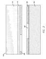
- FIG. 2is a cross-sectional plan view of one of the steps of a preferred method of the present invention
- FIG. 1a preferred embodiment of an integrated MEMS and semiconductor electrical circuit sensor 100 of the present invention is shown.
- the MEMS sensor 100comprises a top or device layer 102 a middle layer 104 and a bottom or handle layer 106 .
- the top layer 102is comprised of a thin semiconductor layer which in a preferred embodiment is a silicon wafer.
- the bottom layer 106provides the support structure for the sensor 100 and, in a preferred embodiment, is a handle wafer comprised of silicon.
- the middle layer 104is comprised of silicon oxide. However, any material which acts as an non-conductive and/or insulating material can be used.
- a cavity 108is formed in the middle layer 104 by either etching or masking the layer 104 .
- any suitable method for creating a cavity 108may be used.
- the cavitymay be formed in the base layer 106 or in the top layer 102 with suitable modifications of the device 100 .
- the top layer 102acts as both the substrate of the semiconductor electrical circuit and as the active mechanical element.
- the semiconductor electrical circuitis fabricated on the thin upper silicon layer 102 .
- the semiconductor electrical circuit in FIG. 1comprises a plurality of CMOS devices in which implant areas 116 a and 116 b are shown over which gates 118 of the CMOS devices are placed. Additional electronics may also be placed on or in layer 102 .
- an additional layer of insulating materialpartially covering the top layer 102 onto which additional semiconductor electrical circuitry such as the gates or other electronics may be placed.
- the MEMS sensor 100is formed by taking a silicon wafer 106 and growing silicon oxide or another insulating material on the top thereof to form layer 104 .
- a cavity 108is etched in layer 104 .
- any method of creating a clearly defined cavity in any of the layersmay be used.
- an SOI wafer 110comprising a thin silicon layer 102 , an insulating layer 114 and a handle layer 116 is then placed on layer 104 so that the thin silicon layer 102 rests across the entire layer 104 .
- a solid SI wafer which has been thinned downmay be used in place of the SOI wafer.
- the layersare bonded together by high temperature fusing.
- temperatures of approximately 1000° C.are used.
- any eutectic or anodic bondingcan also be used with suitable modifications.
- any process which provides a strong bond and produces a controlled, well defined and well sealed cavity in any of the layersmay be used.
- the handle layer 116 of the SOI wafer 110is removed leaving the top thin silicon layer 102 and the insulating layer 114 .
- all or part of the insulating layer 114 of the SOI wafer 110may be removed.
- the remainder of the semiconductor electrical circuitryis then fabricated onto the thin upper silicon layer 102 .
- implant areassuch as areas 116 a and 116 b , which comprise source and drain pads, are formed in the thin upper silicon layer 102 .
- additional circuitry or components which need to be isolated from the silicon layer 102may be placed on top of the insulating layer 114 .
- the semiconductor electrical circuitrycan be fabricated in or on the base layer 106 .
- the semiconductor electrical circuits and implant areasare created after the fabrication of the MEMS structure.
- the semiconductor electrical circuitsare located on or in the thin upper layer 102 , there is no longer a need to isolate the components of the semiconductor electrical circuits from the MEMS.
- the sensorscan be made much smaller and thus, can be used in many different applications.
- the present inventionallows for integration of sensors with submicron semiconductor electrical circuits which enables more complex signal processing, on-chip calibration and integration with RF technologies for development of wireless sensor networks.
- the inventionalso allows for the creation of suspended structures that could be released at the final step when all of the semiconductor electrical circuit processing has been completed.
- this type fabricationcan be used in pressure sensors, accelerometers, force sensors, humidity sensors and in switches used in TPMS, MAP, and in automotive, medical, airplane, heating, ventilating, air conditioning systems (HVAC), as well as other industrial and consumer, applications.
- HVACheating, ventilating, air conditioning systems
Landscapes
- Engineering & Computer Science (AREA)
- Manufacturing & Machinery (AREA)
- Microelectronics & Electronic Packaging (AREA)
- Micromachines (AREA)
- Pressure Sensors (AREA)
Abstract
Description
Claims (20)
Priority Applications (6)
| Application Number | Priority Date | Filing Date | Title |
|---|---|---|---|
| US12/404,792US8196475B2 (en) | 2009-03-16 | 2009-03-16 | Cointegrated MEMS sensor and method |
| DE102010011631ADE102010011631A1 (en) | 2009-03-16 | 2010-03-16 | Co-integrated MEMS sensor and method for this |
| JP2010060022AJP5486360B2 (en) | 2009-03-16 | 2010-03-16 | Co-embedded MEMS sensor and method thereof |
| JP2012253121AJP2013056415A (en) | 2009-03-16 | 2012-11-19 | Cointegrated mems sensor and method for the same |
| JP2013176320AJP2014014927A (en) | 2009-03-16 | 2013-08-28 | Co-integrated mems sensor and method of the same |
| JP2014206126AJP2015057305A (en) | 2009-03-16 | 2014-10-07 | Co-integrated mems sensor and method of the same |
Applications Claiming Priority (1)
| Application Number | Priority Date | Filing Date | Title |
|---|---|---|---|
| US12/404,792US8196475B2 (en) | 2009-03-16 | 2009-03-16 | Cointegrated MEMS sensor and method |
Publications (2)
| Publication Number | Publication Date |
|---|---|
| US20100229651A1 US20100229651A1 (en) | 2010-09-16 |
| US8196475B2true US8196475B2 (en) | 2012-06-12 |
Family
ID=42729597
Family Applications (1)
| Application Number | Title | Priority Date | Filing Date |
|---|---|---|---|
| US12/404,792Active2029-07-22US8196475B2 (en) | 2009-03-16 | 2009-03-16 | Cointegrated MEMS sensor and method |
Country Status (3)
| Country | Link |
|---|---|
| US (1) | US8196475B2 (en) |
| JP (4) | JP5486360B2 (en) |
| DE (1) | DE102010011631A1 (en) |
Cited By (1)
| Publication number | Priority date | Publication date | Assignee | Title |
|---|---|---|---|---|
| WO2016163636A1 (en)* | 2015-04-08 | 2016-10-13 | 주식회사 스탠딩에그 | Method for preparing mems device |
Families Citing this family (1)
| Publication number | Priority date | Publication date | Assignee | Title |
|---|---|---|---|---|
| FR3048425B1 (en)* | 2016-03-07 | 2021-02-12 | Soitec Silicon On Insulator | STRUCTURE FOR DEVICE WITH INTEGRATED ELECTROMECHANICAL MICROSYSTEMS |
Citations (18)
| Publication number | Priority date | Publication date | Assignee | Title |
|---|---|---|---|---|
| US2993815A (en) | 1959-05-25 | 1961-07-25 | Bell Telephone Labor Inc | Metallizing refractory substrates |
| US4168518A (en) | 1977-05-10 | 1979-09-18 | Lee Shih Y | Capacitor transducer |
| US4206762A (en) | 1976-06-21 | 1980-06-10 | Cosman Eric R | Telemetric differential pressure sensing method |
| US4730496A (en) | 1986-06-23 | 1988-03-15 | Rosemount Inc. | Capacitance pressure sensor |
| US6338893B1 (en) | 1998-10-28 | 2002-01-15 | Ngk Spark Plug Co., Ltd. | Conductive paste and ceramic printed circuit substrate using the same |
| US6452238B1 (en)* | 1999-10-04 | 2002-09-17 | Texas Instruments Incorporated | MEMS wafer level package |
| US6460234B1 (en) | 1998-08-19 | 2002-10-08 | Wisconsin Alumni Research Foundation | Method of forming micromachined sealed capacitive pressure sensors |
| US6516672B2 (en) | 2001-05-21 | 2003-02-11 | Rosemount Inc. | Sigma-delta analog to digital converter for capacitive pressure sensor and process transmitter |
| US6660564B2 (en)* | 2002-01-25 | 2003-12-09 | Sony Corporation | Wafer-level through-wafer packaging process for MEMS and MEMS package produced thereby |
| US6819820B1 (en)* | 2000-11-29 | 2004-11-16 | Analog Devices, Inc. | Use of applied force to improve MEMS switch performance |
| US6872319B2 (en)* | 2002-09-30 | 2005-03-29 | Rockwell Scientific Licensing, Llc | Process for high yield fabrication of MEMS devices |
| US6952042B2 (en) | 2002-06-17 | 2005-10-04 | Honeywell International, Inc. | Microelectromechanical device with integrated conductive shield |
| US7071016B2 (en)* | 2002-11-27 | 2006-07-04 | Samsung Electro-Mechanics Co., Ltd. | Micro-electro mechanical systems (MEMS) device using silicon on insulator (SOI) wafer, and method of fabricating and grounding the same |
| US7209274B2 (en)* | 2001-06-02 | 2007-04-24 | Capella Photonics, Inc. | High fill-factor bulk silicon mirrors |
| US20070199385A1 (en) | 2005-11-18 | 2007-08-30 | Cardiomems, Inc. | Capacitor electrode formed on surface of integrated circuit chip |
| US7456497B2 (en)* | 2002-12-27 | 2008-11-25 | Shinko Electric Industries Co., Ltd. | Electronic devices and its production methods |
| US7781238B2 (en)* | 2007-12-06 | 2010-08-24 | Robert Gideon Wodnicki | Methods of making and using integrated and testable sensor array |
| US7851925B2 (en)* | 2008-09-19 | 2010-12-14 | Infineon Technologies Ag | Wafer level packaged MEMS integrated circuit |
Family Cites Families (10)
| Publication number | Priority date | Publication date | Assignee | Title |
|---|---|---|---|---|
| US1468518A (en)* | 1921-02-05 | 1923-09-18 | Robert W Scott | Knitting-machine needle |
| DE69627645T2 (en)* | 1996-07-31 | 2004-02-05 | Stmicroelectronics S.R.L., Agrate Brianza | Integrated piezoresistive pressure transducer and manufacturing process |
| DE69626972T2 (en)* | 1996-07-31 | 2004-01-08 | Stmicroelectronics S.R.L., Agrate Brianza | Integrated capacitive semiconductor acceleration sensor and method for its production |
| US7381630B2 (en)* | 2001-01-02 | 2008-06-03 | The Charles Stark Draper Laboratory, Inc. | Method for integrating MEMS device and interposer |
| JP4278960B2 (en)* | 2002-08-08 | 2009-06-17 | 富士通コンポーネント株式会社 | Micro relay and method of manufacturing micro relay |
| US7329923B2 (en)* | 2003-06-17 | 2008-02-12 | International Business Machines Corporation | High-performance CMOS devices on hybrid crystal oriented substrates |
| JP4359923B2 (en)* | 2004-01-20 | 2009-11-11 | 京セラ株式会社 | Manufacturing method of electromechanical switch |
| JP2007100573A (en)* | 2005-10-04 | 2007-04-19 | Matsushita Electric Ind Co Ltd | Micro pump |
| JP2007157511A (en)* | 2005-12-06 | 2007-06-21 | Hitachi Ltd | Switch using microelectromechanical system |
| US20070180916A1 (en)* | 2006-02-09 | 2007-08-09 | General Electric Company | Capacitive micromachined ultrasound transducer and methods of making the same |
- 2009
- 2009-03-16USUS12/404,792patent/US8196475B2/enactiveActive
- 2010
- 2010-03-16DEDE102010011631Apatent/DE102010011631A1/ennot_activeCeased
- 2010-03-16JPJP2010060022Apatent/JP5486360B2/ennot_activeExpired - Fee Related
- 2012
- 2012-11-19JPJP2012253121Apatent/JP2013056415A/enactivePending
- 2013
- 2013-08-28JPJP2013176320Apatent/JP2014014927A/enactivePending
- 2014
- 2014-10-07JPJP2014206126Apatent/JP2015057305A/ennot_activeWithdrawn
Patent Citations (22)
| Publication number | Priority date | Publication date | Assignee | Title |
|---|---|---|---|---|
| US2993815A (en) | 1959-05-25 | 1961-07-25 | Bell Telephone Labor Inc | Metallizing refractory substrates |
| US4206762A (en) | 1976-06-21 | 1980-06-10 | Cosman Eric R | Telemetric differential pressure sensing method |
| US4168518A (en) | 1977-05-10 | 1979-09-18 | Lee Shih Y | Capacitor transducer |
| US4730496A (en) | 1986-06-23 | 1988-03-15 | Rosemount Inc. | Capacitance pressure sensor |
| US6470754B1 (en) | 1998-08-19 | 2002-10-29 | Wisconsin Alumni Research Foundation | Sealed capacitive pressure sensors |
| US6460234B1 (en) | 1998-08-19 | 2002-10-08 | Wisconsin Alumni Research Foundation | Method of forming micromachined sealed capacitive pressure sensors |
| US6338893B1 (en) | 1998-10-28 | 2002-01-15 | Ngk Spark Plug Co., Ltd. | Conductive paste and ceramic printed circuit substrate using the same |
| US6743656B2 (en)* | 1999-10-04 | 2004-06-01 | Texas Instruments Incorporated | MEMS wafer level package |
| US6452238B1 (en)* | 1999-10-04 | 2002-09-17 | Texas Instruments Incorporated | MEMS wafer level package |
| US6888979B2 (en)* | 2000-11-29 | 2005-05-03 | Analog Devices, Inc. | MEMS mirrors with precision clamping mechanism |
| US6819820B1 (en)* | 2000-11-29 | 2004-11-16 | Analog Devices, Inc. | Use of applied force to improve MEMS switch performance |
| US6516672B2 (en) | 2001-05-21 | 2003-02-11 | Rosemount Inc. | Sigma-delta analog to digital converter for capacitive pressure sensor and process transmitter |
| US7209274B2 (en)* | 2001-06-02 | 2007-04-24 | Capella Photonics, Inc. | High fill-factor bulk silicon mirrors |
| US6660564B2 (en)* | 2002-01-25 | 2003-12-09 | Sony Corporation | Wafer-level through-wafer packaging process for MEMS and MEMS package produced thereby |
| US6841861B2 (en)* | 2002-01-25 | 2005-01-11 | Sony Corporation | MEMS package |
| US6952042B2 (en) | 2002-06-17 | 2005-10-04 | Honeywell International, Inc. | Microelectromechanical device with integrated conductive shield |
| US6872319B2 (en)* | 2002-09-30 | 2005-03-29 | Rockwell Scientific Licensing, Llc | Process for high yield fabrication of MEMS devices |
| US7071016B2 (en)* | 2002-11-27 | 2006-07-04 | Samsung Electro-Mechanics Co., Ltd. | Micro-electro mechanical systems (MEMS) device using silicon on insulator (SOI) wafer, and method of fabricating and grounding the same |
| US7456497B2 (en)* | 2002-12-27 | 2008-11-25 | Shinko Electric Industries Co., Ltd. | Electronic devices and its production methods |
| US20070199385A1 (en) | 2005-11-18 | 2007-08-30 | Cardiomems, Inc. | Capacitor electrode formed on surface of integrated circuit chip |
| US7781238B2 (en)* | 2007-12-06 | 2010-08-24 | Robert Gideon Wodnicki | Methods of making and using integrated and testable sensor array |
| US7851925B2 (en)* | 2008-09-19 | 2010-12-14 | Infineon Technologies Ag | Wafer level packaged MEMS integrated circuit |
Cited By (2)
| Publication number | Priority date | Publication date | Assignee | Title |
|---|---|---|---|---|
| WO2016163636A1 (en)* | 2015-04-08 | 2016-10-13 | 주식회사 스탠딩에그 | Method for preparing mems device |
| KR20160120564A (en)* | 2015-04-08 | 2016-10-18 | 주식회사 스탠딩에그 | Method of manufacturing mems device |
Also Published As
| Publication number | Publication date |
|---|---|
| JP5486360B2 (en) | 2014-05-07 |
| US20100229651A1 (en) | 2010-09-16 |
| DE102010011631A1 (en) | 2010-10-21 |
| JP2014014927A (en) | 2014-01-30 |
| JP2015057305A (en) | 2015-03-26 |
| JP2013056415A (en) | 2013-03-28 |
| JP2010214584A (en) | 2010-09-30 |
Similar Documents
| Publication | Publication Date | Title |
|---|---|---|
| US9709451B2 (en) | Micromechanical pressure sensor device and corresponding manufacturing method | |
| KR101976257B1 (en) | System and method for a transducer in an ewlb package, and the ewlb package | |
| US9926188B2 (en) | Sensor unit including a decoupling structure and manufacturing method therefor | |
| CN106257254B (en) | Pressure sensor generating a transducing signal with reduced ambient temperature dependency and method of manufacturing the same | |
| US7560788B2 (en) | Microelectromechanical system pressure sensor and method for making and using | |
| CN103335753B (en) | The ultra-miniature pressure sensor chip of si-glass base beam diaphragm structure and manufacture method | |
| US8884385B2 (en) | Physical quantity sensor with son structure, and manufacturing method thereof | |
| CN105940287A (en) | Micromechanical pressure sensor apparatus and associated production method | |
| US20070275495A1 (en) | Method for fabricating a pressure sensor using SOI wafers | |
| CN102674237A (en) | Monolithic integrated sensor device and method thereof and method for formign the cavity structure of the monolithic integrated sensor device | |
| US10317211B2 (en) | Robust inertial sensors | |
| US10858245B2 (en) | Deposition of protective material at wafer level in front end for early stage particle and moisture protection | |
| KR20160088111A (en) | Complex sensor, package having the same and manufacturing method thereof | |
| US9725298B2 (en) | CMOS integrated moving-gate transducer with silicon as a functional layer | |
| US20100187646A1 (en) | Ultra low pressure sensor and method of fabrication of same | |
| US8196475B2 (en) | Cointegrated MEMS sensor and method | |
| US20090283846A1 (en) | Backside controlled mems capacitive sensor and interface and method | |
| US10209155B2 (en) | Physical quantity sensing semiconductor device and method for manufacturing the same | |
| CN207800604U (en) | A kind of integrating device of chip | |
| JP2777559B2 (en) | Semiconductor element sensor having a welded deformable portion | |
| US8853800B2 (en) | Integrated device of the type comprising at least a microfluidic system and further circuitry and corresponding integration process | |
| CN109540371A (en) | Pressure sensor and manufacturing method thereof | |
| JP2015068728A (en) | Physical quantity sensor, atmosphere pressure sensor, electronic apparatus, and moving body | |
| JP6142735B2 (en) | Semiconductor pressure sensor | |
| CN102967407B (en) | A kind of absolute pressure sensor die and preparation method thereof |
Legal Events
| Date | Code | Title | Description |
|---|---|---|---|
| AS | Assignment | Owner name:KAVLICO CORPORATION, CALIFORNIA Free format text:ASSIGNMENT OF ASSIGNORS INTEREST;ASSIGNORS:SEESINK, PETER;OBERMEIER, HORST;ABED, OMAR;AND OTHERS;SIGNING DATES FROM 20090309 TO 20090515;REEL/FRAME:022999/0915 | |
| STCF | Information on status: patent grant | Free format text:PATENTED CASE | |
| AS | Assignment | Owner name:DEUTSCHE BANK AG NEW YORK BRANCH, AS COLLATERAL AG Free format text:SECURITY AGREEMENT;ASSIGNORS:BEI SENSORS & SYSTEMS COMPANY, INC.;CUSTOM SENSORS & TECHNOLOGIES, INC;CRYDOM, INC.;AND OTHERS;REEL/FRAME:033888/0700 Effective date:20140930 | |
| AS | Assignment | Owner name:CUSTOM SENSORS & TECHNOLOGIES, INC., CALIFORNIA Free format text:RELEASE BY SECURED PARTY;ASSIGNOR:DEUTSCHE BANK AG NEW YORK BRANCH;REEL/FRAME:037196/0174 Effective date:20151201 Owner name:CRYDOM, INC., CALIFORNIA Free format text:RELEASE BY SECURED PARTY;ASSIGNOR:DEUTSCHE BANK AG NEW YORK BRANCH;REEL/FRAME:037196/0174 Effective date:20151201 Owner name:KAVLICO CORPORATION, CALIFORNIA Free format text:RELEASE BY SECURED PARTY;ASSIGNOR:DEUTSCHE BANK AG NEW YORK BRANCH;REEL/FRAME:037196/0174 Effective date:20151201 Owner name:BEI SENSORS & SYSTEMS COMPANY, INC., CALIFORNIA Free format text:RELEASE BY SECURED PARTY;ASSIGNOR:DEUTSCHE BANK AG NEW YORK BRANCH;REEL/FRAME:037196/0174 Effective date:20151201 Owner name:BEI TECHNOLOGIES, INC., CALIFORNIA Free format text:RELEASE BY SECURED PARTY;ASSIGNOR:DEUTSCHE BANK AG NEW YORK BRANCH;REEL/FRAME:037196/0174 Effective date:20151201 | |
| FPAY | Fee payment | Year of fee payment:4 | |
| AS | Assignment | Owner name:MORGAN STANLEY SENIOR FUNDING, INC., NEW YORK Free format text:SECURITY INTEREST;ASSIGNORS:BEI NORTH AMERICA LLC;CRYDOM, INC.;CUSTOM SENSORS & TECHNOLOGIES, INC.;AND OTHERS;REEL/FRAME:037927/0605 Effective date:20160224 | |
| MAFP | Maintenance fee payment | Free format text:PAYMENT OF MAINTENANCE FEE, 8TH YEAR, LARGE ENTITY (ORIGINAL EVENT CODE: M1552); ENTITY STATUS OF PATENT OWNER: LARGE ENTITY Year of fee payment:8 | |
| MAFP | Maintenance fee payment | Free format text:PAYMENT OF MAINTENANCE FEE, 12TH YEAR, LARGE ENTITY (ORIGINAL EVENT CODE: M1553); ENTITY STATUS OF PATENT OWNER: LARGE ENTITY Year of fee payment:12 |