US8195839B2 - Apparatus and method for producing identifiers regardless of mixed device type in a serial interconnection - Google Patents
Apparatus and method for producing identifiers regardless of mixed device type in a serial interconnectionDownload PDFInfo
- Publication number
- US8195839B2 US8195839B2US12/892,215US89221510AUS8195839B2US 8195839 B2US8195839 B2US 8195839B2US 89221510 AUS89221510 AUS 89221510AUS 8195839 B2US8195839 B2US 8195839B2
- Authority
- US
- United States
- Prior art keywords
- devices
- serial
- determination
- signal
- received
- Prior art date
- Legal status (The legal status is an assumption and is not a legal conclusion. Google has not performed a legal analysis and makes no representation as to the accuracy of the status listed.)
- Expired - Fee Related
Links
Images


Classifications
- G—PHYSICS
- G11—INFORMATION STORAGE
- G11C—STATIC STORES
- G11C7/00—Arrangements for writing information into, or reading information out from, a digital store
- G11C7/10—Input/output [I/O] data interface arrangements, e.g. I/O data control circuits, I/O data buffers
- G11C7/1078—Data input circuits, e.g. write amplifiers, data input buffers, data input registers, data input level conversion circuits
- G—PHYSICS
- G11—INFORMATION STORAGE
- G11C—STATIC STORES
- G11C7/00—Arrangements for writing information into, or reading information out from, a digital store
- G11C7/10—Input/output [I/O] data interface arrangements, e.g. I/O data control circuits, I/O data buffers
- G11C7/1051—Data output circuits, e.g. read-out amplifiers, data output buffers, data output registers, data output level conversion circuits
- G11C7/1063—Control signal output circuits, e.g. status or busy flags, feedback command signals
- G—PHYSICS
- G11—INFORMATION STORAGE
- G11C—STATIC STORES
- G11C7/00—Arrangements for writing information into, or reading information out from, a digital store
- G11C7/10—Input/output [I/O] data interface arrangements, e.g. I/O data control circuits, I/O data buffers
- G11C7/1078—Data input circuits, e.g. write amplifiers, data input buffers, data input registers, data input level conversion circuits
- G11C7/109—Control signal input circuits
Definitions
- the present inventionrelates generally to semiconductor device systems. More particularly, the present invention relates to apparatus and method for producing device identifiers for a serial interconnection configuration of devices of mixed type.
- Non-volatile memory and hard disk drivesare preferred since data is retained in the absence of power, thus extending battery life.
- the memorycommunicates with other components using a set of parallel input/output (I/O) pins, the number of which depends on the desired configuration.
- the I/O pinsreceive command instructions and input data and provides output data. This is commonly known as a parallel interface. High speed operation may cause deleterious communication effects such as, for example, cross-talk, signal skew and signal attenuation, which degrade signal quality.
- multi-drop and serial interconnection configurationsIn order to incorporate higher density and faster operation on the system boards, there are two design techniques possible: multi-drop and serial interconnection configurations. These design techniques may be used to overcome the density issue that determines the cost and operating efficiency of memory swapping between a hard disk and a memory system.
- multi-drop configurationshave shortcomings relative to the serial interconnection of memory systems. For example, if the number of multi-drop memory systems increases, as a result of the loading effect of each pin, the delay time also increases so that the total performance of multi-drop is degraded by the multi-drop connection caused by the wire resistor-capacitor loading and the pin capacitance of the memory device.
- a serial linkmay provide a serial interconnection configuration to control command bits, address bits, and data bits effectively through the serial interconnection. In the serial interconnection configuration, each device is identified by a device identifier or a device address.
- a systemcomprising: a signal processor capable of outputting a serial input signal and receiving a serial output signal; and a serial interconnection configuration of first to N-th devices of mixed type, N being an integer greater than one.
- Each of the deviceshas a serial input connection and a serial output connection.
- Each of the devicesis capable of determining a device type (DT) and providing a combination of the DT and a device identifier (ID).
- the serial input connection of one of the devicesis coupled to the signal processor or the serial output connection of a previous device.
- the serial output connection of the one of the devicesis coupled to the serial input connection of a next device or the signal processor.
- the serial signal provided to the serial input connection of the first device from the signal processoris propagated through the N devices with or without being altered.
- the propagated serial input signalis outputted from the serial output connection of the N-th device as the serial output signal received by the signal processor.
- each of the devicescomprises: a receiver for receiving an ID and a DT provided through the serial input connection of the device; a determiner for determining the DT of the device from the received DT; an output ID provider for outputting an ID in response to a determination result; an information provider for providing a combination of the received DT and the outputted ID; and a device type provider for providing device type information (DTI) associated with the device as a reference DT.
- DTIdevice type information
- the output ID providerincludes: a calculator for performing a calculation based on the received ID and a pre-defined value to produce a calculated ID; and a selector for selecting the received ID or the calculated ID in response to the determination result, the selected ID being outputted from the ID provider.
- the determinerincludes a comparator for comparing the received DT with the reference DT to provide the determination result.
- a selectormay select the received ID or the calculated ID in response to the determination result. The selected ID being outputted to the information provider.
- the DT and IDare transmitted as a packet.
- the packetincludes an ID generation command.
- a packet interpretermay interpret the ID generation command and the received DT.
- the information providermay further include a combiner for combining the ID generation command, the DT and the ID; and a packet output provider for providing the combined command, DT and ID as a packet.
- a method for assigning a device identifier for a plurality of devices of mixed type in a serial interconnection configurationa first device having a serial input connection coupled to a serial output connection of a previous device, a second device having a serial input connection coupled to a serial output connection of the first device, the method being adopted to at least one of the devices.
- the methodcomprises: receiving a device identifier (ID) and a device type (DT) through the serial input connection of the first device; performing: a first determination of whether the DT of the device contains pre-defined data corresponding to one including all device types to provide a first determination result; and a second determination of the DT of the device in response to the received DT to provide a second determination result; and outputting a device ID in response to the first and second determination results.
- IDdevice identifier
- DTdevice type
- the step of performingcomprises: performing the first determination whether the received DT of the device matches a pre-defined data; and performing the second determination of whether the received DT matches a reference DT assigned to the device.
- the step of the first determinationcomprises: providing a pre-defined value as the pre-defined data that corresponds to any of the types of devices.
- the step of performing the second determinationcomprises: providing the reference DT programmably.
- the first determinationis performed by a decoder for decoding the received DT to produce the first determination result when the pre-defined data is detected.
- the second determinationis performed by a comparator to compare the received DT with the provided reference DT to provide the second determination result.
- the first determinationis performed by another comparator for comparing the received DT with the pre-defined data to make a decision whether the pre-defined data is contained in the received DT.
- an apparatus for assigning a device identifier at a first device coupled to a second device in a serial interconnection configurationthe first device having a serial input connection coupled to a serial output connection of a previous device in the serial interconnection configuration
- the second devicehaving a serial input connection coupled to a serial output connection of the first device, the devices being of different types.
- the apparatuscomprises: a receiver for receiving an ID and a device type (DT) provided through the serial input connection of the device; a determiner for performing: a first determination of whether the DT of the device contains pre-defined data corresponding to one including all device types to provide a first determination result; and a second determination of the DT of the device based on the received DT to provide a second determination result; and an output ID provider for outputting a device identifier (ID) in response to the first and second determination results.
- DTdevice type
- the output ID providercomprises: a calculator for performing the calculation of the received ID with a pre-defined value; and a selector for selecting the received ID or the calculated ID depending upon the determination result, the selected ID being outputted through the output connection of the device.
- the apparatusmay further comprise a device type provider for providing device type information (DTI) of the device.
- DTIdevice type information
- the determinercomprises: a first comparator for comparing the received DT with the pre-defined data to provide the first determination result; and a second comparator for comparing the received DT with the provided DTI to provide the second determination result.
- a systemcomprising a plurality of devices of mixed type in a serial interconnection configuration, a first device having a serial input connection coupled to a serial output connection of a previous device, a second device having a serial input connection coupled to a serial output connection of the first device.
- At least one of the devicescomprises: a receiver for receiving a device identifier (ID) and a device type (DT) provided through the serial input connection of the device; a determiner for determining the DT of the device based on the received DT or whether the DT of the device contains pre-defined data corresponding to one including all device types; and an output ID provider for outputting an ID in response to the determination result.
- IDdevice identifier
- DTdevice type
- a method for assigning a device identifier for a plurality of devices of mixed type in a serial interconnection configurationa first device having a serial input connection coupled to a serial output connection of a previous device, a second device having a serial input connection coupled to a serial output connection of the first device.
- the methodcomprises: providing a device type (DT) to a device; holding the provided DT at the device; determining whether the DT matches a reference DT associated with the device; determining whether the DT of the device contains pre-defined data corresponding to one including all device types; outputting a device identifier (ID) to one of the device in the serial interconnection configuration, through the serial input connection of that device; and at the device wherein the ID is provided, conducting an ID assignment in response to the determination results at that device.
- DTdevice type
- a method for assigning a device identifier associated with a serial interconnection configuration of N devices of mixed typecomprising: at each of the devices, determining a device type (DT); providing a serial input signal to the first device of the serial interconnection configuration, the serial input signal being propagated through the N devices with or without being altered; and in response to a serial output signal from the N-th device provided to the signal processor, recognizing a last device identifier (ID).
- DTdevice type
- the step of recognizingcomprises: performing the recognition of the number of the devices in response to the recognized last ID.
- a method for use in a serial interconnection configuration of N devices of mixed typecomprising: providing a serial input signal to the first device of the serial interconnection configuration, the serial input signal being propagated through the N device with or without being altered; and receiving a serial output signal provided from the N-th device.
- the step of receivingcomprises: recognizing an ID number contained in the propagated serial input signal from the serial output connection of the N-th device.
- the step of providingcomprises: providing a unique DT accompanied with an initial ID number contained in the serial input signal to the first device of the serial interconnection configuration, the unique DT matching any of the types of the devices, the propagated serial input signal containing an ID number altered by the device in response to a determination result.
- the step of recognizingcomprises: receiving the propagated serial output signal containing the ID number accompanied with the unique DT from the N-th device; and recognizing the number of the devices in the serial interconnection configuration based on the received ID number.
- the step of providingmay further comprise: providing an ID generation command; and combining the ID generation command, the initial ID number and the unique DT.
- the DT and IDare transmitted as a packet.
- a machine-readable mediumstoring commands and instructions which, when executed, cause a processor to perform a method of receiving an output signal from a last device of N devices of mixed type in a serial interconnection, N being an integer greater than one, a first device having a serial input connection coupled to a serial output connection of a previous device, a second device having a serial input connection coupled to a serial output connection of the first device, each of the devices determining a device type (DT) and providing a combination of the DT and a device identifier (ID).
- the methodcomprises: providing a serial input signal to the first device of the serial interconnection configuration, the serial input signal being propagated through the N device with or without being altered; and receiving a serial output signal provided from the N-th device.
- a machine-readable mediumstoring commands and instructions which, when executed, cause a processor to perform a method of assigning a device identifier (ID) for a plurality of devices of mixed type in a serial interconnection configuration, a first device having a serial input connection coupled to a serial output connection of a previous device, a second device having a serial input connection coupled to a serial output connection of the first device, the method being adopted to at least one of the devices.
- IDdevice identifier
- the methodcomprises: receiving an ID and a device type (DT) through the serial input connection of the first device; performing: a first determination of whether the DT of the device contains pre-defined data corresponding to one including all device types to provide a first determination result; and a second determination of the DT of the device in response to the received DT to provide a second determination result; and outputting a device ID in response to the first and second determination results.
- DTdevice type
- a plurality of memory devices of mixed typethat is serially interconnected.
- the devicesare, for example, random access memories and Flash memories.
- Each devicehas device type information on its device type.
- An ID generation command, a specific device type (DT) and a device identifier (ID)are provided by a memory controller to a device that determines whether the fed DT matches the device's DT. If there is a match between them, an addition of ID is performed in the device to produce an ID. If there is no DT match, no addition is performed in the device (i.e., the ID production is skipped or bypassed).
- the added ID(the produced ID) or the fed ID (the non-calculated ID) is selected and the selected ID accompanying the fed DT is transferred to a next device in the serial interconnection configuration.
- a device type match determination and ID production or skipare performed in all devices of the serial interconnection configuration.
- IDsare sequentially generated.
- the Serial Input (SI) containing the DT, the ID and an ID generation commandis transmitted in a packet basis to a next device.
- the memory controllercan recognize the total number of one DT, in response to the ID received from the last device. In a case of a “don't care” DT is provided to the interconnected devices, IDs are sequentially generated and the total number of the interconnected devices is recognized, regardless of the difference in DTs.
- an ID generation with skip functionfor serially interconnected memory devices of mixed type, in accordance with the device types.
- the devicesmay be random access memories such as dynamic random access memory (DRAM), static random access memory (SRAM), magnetoresistive random access memory (MRAM) and Flash memories such as NAND-, NOR- and AND-types.
- DRAMdynamic random access memory
- SRAMstatic random access memory
- MRAMmagnetoresistive random access memory
- Flash memoriessuch as NAND-, NOR- and AND-types.
- FIG. 1is a block diagram illustrating a system including a plurality of devices in a serial interconnection configuration to which embodiments of the present invention are applied;
- FIG. 2Ais a block diagram illustrating the system including part of the plurality of devices in the serial interconnection configuration shown in FIG. 1 ;
- FIG. 2Bis a block diagram illustrating one of the devices shown in FIG. 2A ;
- FIG. 2Cis a block diagram illustrating an example of a device operation controller shown in FIG. 2B ;
- FIG. 2Dis a block diagram illustrating an example of an ID generator shown in FIG. 2B ;
- FIG. 3Ais a flow chart of operation performed by the serial interconnection configuration of FIG. 2A ;
- FIG. 3Bis a flow chart of part of the operation shown in FIG. 3A ;
- FIG. 4Ais a block diagram illustrating the plurality of devices in the serial interconnection configuration shown in FIG. 2A , in which NAND Flash devices perform an ID generation;
- FIG. 4Bis a timing diagram of the ID generation in the serial interconnection configuration of FIG. 4A ;
- FIG. 5Ais a block diagram illustrating the plurality of devices in the serial interconnection configuration shown in FIG. 2A , in which NOR Flash devices perform an ID generation;
- FIG. 5Bis a timing diagram of the ID generation in the serial interconnection configuration of FIG. 5A ;
- FIG. 6Ais a schematic diagram illustrating a protocol conducted in the devices shown in FIG. 1 , wherein NAND Flash devices generate IDs;
- FIG. 6Bis a schematic diagram illustrating a protocol conducted in the devices shown in FIG. 1 , wherein NOR Flash devices generate IDs;
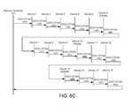
- FIG. 6Cis a schematic diagram illustrating a protocol conducted in the devices shown in FIG. 1 , wherein DRAM devices generate IDs;
- FIG. 6Dis a schematic diagram illustrating a protocol conducted in the devices shown in FIG. 1 , wherein SRAM devices generate IDs;
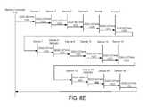
- FIG. 6Eis a schematic diagram illustrating a protocol conducted in the devices shown in FIG. 1 , wherein MRAM devices generate IDs;
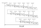
- FIG. 6Fis a schematic diagram illustrating a protocol conducted in the devices shown in FIG. 1 , wherein no devices generate IDs;
- FIG. 7Ais a block diagram illustrating another example of the ID generator that is applied to the devices serially interconnected as shown in FIG. 1 ;
- FIG. 7Bis a block diagram illustrating a DT match detector shown in FIG. 7A ;
- FIG. 7Cis a block diagram illustrating a DT decoder shown in FIG. 7B ;
- FIG. 8is a flow chart illustrating an ID generation method applied to the device shown in FIG. 1 with the ID generator shown in FIG. 7A ;
- FIG. 9Ais a schematic diagram illustrating a protocol conducted in the devices shown in FIG. 1 , wherein all of the devices generate IDs;
- FIG. 9Bis a timing diagram of the ID generation in the serial interconnection configuration, wherein all of the devices generate IDs
- FIG. 10is a block diagram of an example of a memory controller of FIG. 1 ;
- FIG. 11Ais a flowchart illustrating an ID generation method performed by the devices shown in FIG. 1 ;
- FIG. 11Bis a flow chart of part of the ID generation method shown in FIG. 11A ;
- FIG. 12is a schematic diagram illustrating a protocol conducted in the devices shown in FIG. 1 ;
- FIG. 13Ais a block diagram illustrating another example of a DT match detector shown in FIG. 7A ;
- FIG. 13Bis a flow chart illustrating an ID generation method applied to the device shown in FIG. 1 with the ID generator shown in FIG. 13A ;
- FIG. 14is a block diagram illustrating another example of the ID generator wherein an altered ID is registered
- FIG. 15is a block diagram illustrating another example of the ID generator wherein a subtracted ID is generated
- FIG. 16is a block diagram illustrating another example of the ID generator wherein a subtracted ID is registered
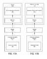
- FIG. 17Ais a block diagram illustrating a machine-readable medium storing commands and instructions for use in a device of FIG. 1 ;
- FIG. 17Bis a block diagram illustrating a machine-readable medium storing commands and instructions for use in a memory controller of FIG. 1 .
- the present inventionprovides apparatus and method for producing device identifiers in serially interconnected devices.
- the command stringmay be fed to all of the devices even though the command may only be performed on one of the devices.
- the command stringmay contain a device identifier (ID) or a device address that identifies the memory device to which the command is directed.
- IDdevice identifier
- Each device receiving the command stringcompares the ID contained in the command string to an ID associated with the device. If the two match, the device will assumes that the command is directed to the device to execute the command.
- the above-described arrangementneeds to assign an ID for each device.
- One technique that may be used to assign an ID for a deviceis to hardwire an internal unique ID into the device.
- One drawback with this approachis that if large volumes of devices are used, the size of the ID may have to be quite large in order to ensure that each device contains a unique ID. Managing a large-sized ID may add significant complexity to the device which in turn may increase the cost of producing the device. In addition, reclaiming IDs that are associated with devices that are no longer in use may further add to the complexity of this scheme.
- IDsmay be specified by wiring various pins on the device to certain states to assign an ID for the device.
- the devicereads the wired state of the pins and assigns its ID from the read state.
- external wiringis needed to assign the ID for each device. This may add to the complexity of, e.g., printed circuit boards (PCBs) that hold the memory devices.
- PCBsprinted circuit boards
- Another drawback with this approachis that it may require pins to be dedicated for the assignment of the ID. This may consume precious resources that may be otherwise better used.
- dedicating pins for the assignment of the IDmay require a greater footprint for the device than if pins were not used to assign the ID.
- At least some of embodiments of the present inventionaddress at least some of these shortcomings. At least some example embodiments automatically assign an ID for a device, for example, in a serial interconnection configuration, in a manner that does not require special internal or external hardwiring of the ID.
- an input signalis transferred to a first device in an arrangement including multiple devices (e.g., a serial interconnection configuration) using inputs that are also used by the first device to input other information to the device (e.g., data, commands, control signals).
- a generatorgenerates an ID in response to the input signal.
- a transmittertransfers an output signal associated with the ID to a second device through a serial output of the first device.
- the serial outputmay also be used by the first device to output other information (e.g., signals, data) to another device in the configuration.
- a write ID operationis initiated at a device in a serial interconnection configuration of memory devices of mixed type to cause the device to produce an ID.
- a first devicereceives information on a device type (DT) and a first value by acquiring the state of one or more inputs of the first device. If the received DT matches the device type of the first device, it will generate an ID from the first value, which may include placing the first value in storage (e.g., an ID register) associated with the device.
- the first devicegenerates a second value from the acquired state.
- the first deviceoutputs a second value via an output of the first device to a second device in the serial interconnection configuration.
- the second deviceinputs the value output by the first device and repeats this process to generate an ID.
- Embodiments of the present inventionwill now be described in conjunction with the ID generation in a packet basis wherein during an ID generation operation, an ID generation command is serially transferred through the serial interconnection of devices.
- a devicereceives serial packet basis commands at the serial input thereof in response to clocks and interprets them for ID generation.
- a packet based ID generationis disclosed in U.S. patent application Ser. No. 11/529,293 filed Sep. 29, 2006 entitled “Packet Based ID Generation for Serially Interconnected Devices”, the content of which is entirely incorporated herein by reference.
- details of ID generation for a serial interconnection configuration of memory devices of mixed typeare disclosed in U.S. Provisional Patent Application No. 60/887,401 filed Jan. 31, 2007, the content of which is entirely incorporated herein by reference.
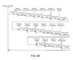
- FIG. 1shows a system including a plurality of (N) devices of mixed type in a serial interconnection configuration and a memory controller, in which embodiments of the present invention are implemented.
- Nis 16 and 16 devices are serially interconnected.
- the devices' typesare mixed and the memory devices included in the serial interconnection configuration are of any type of memories, such as, for example, random access memories and Flash memories.
- the random access memoriesare DRAM, SRAM and MRAM and the Flash memories are NAND-type, NOR-type, AND-type, and other types of Flash memories.
- the random access memoriesare DRAM, SRAM and MRAM
- the Flash memoriesare NAND-type, NOR-type, AND-type, and other types of Flash memories.
- FIG. 1shows a system including a plurality of (N) devices of mixed type in a serial interconnection configuration and a memory controller, in which embodiments of the present invention are implemented.
- Nis 16 and 16 devices are serially interconnected.
- the devices' typesare mixed and the memory devices included in
- a signal processorsuch as, for example, a memory controller 110 is connected to the first and last devices in the serial interconnection configuration.
- the memory controller 110sends a serial input SI from its signal output connection (SOC) to device 1, 120 - 1 , and receives a serial output SO at its signal input connection (SIC) from device 16, 120 - 16 .
- SOCsignal output connection
- SICsignal input connection
- serial interconnection configuration shown in FIG. 1includes NAND and NOR Flash devices and DRAM, SRAM and MRAM devices only. Those of ordinary skill in the art understand that the serial interconnection configuration, such as the one shown in FIG. 1 , can include any other type of memory devices.
- the data inputted as the SI to a serial input port (SIP) connection of each devicecontains various information for system operation.
- the SIincludes data to be processed by an intended device (e.g., device 3) and its processed data is outputted as serial output data from its serial output port (SOP) connection.
- an intended device for receipt of the serial dataneeds to be identified for data processing.
- Such an identifieris attached to the serial data as an ID.
- the ID for device 3, 120 - 3is provided by the memory controller 110 .
- the size of the IDdepends on the requirements of the system.
- device 3provides a serial output SO 3 from its SOP connection, the SO 3 being fed, as the S 14 , to device 4, 120 - 4 .
- device 120 - 4provides a serial output SO 4 , as the S 15 , to device 5, 120 - 5 .
- each devicereceives serial input data through its SIP connection from a previous device and provides serial output data to a next device through its SOP connection.
- IDsare generated and assigned to relevant devices.
- FIG. 2Ashows details of part of the system of FIG. 1 .
- part of the serial interconnection configurationincludes devices 1-5 ( 120 - 1 - 120 - 5 ), which include memories 220 - 1 - 220 - 5 therein, respectively.
- Each of the memories 220 - 1 , 220 - 3 and 220 - 5is a NAND-type Flash memory.
- Each of the memories 220 - 2 and 220 - 4is a NOR-type Flash memory.
- a system implementing such an arrangement of different type or a mixed-device serial interconnectionmay require that only devices of a certain type (e.g., NAND Flash devices) be assigned IDs.
- the systemmay require that all devices be assigned IDs, but that all devices of the same type be assigned IDs in a consecutive sequence.
- devices 1-5120 - 1 - 120 - 5
- device controllers 230 - 1 - 230 - 5are provided with device controllers 230 - 1 - 230 - 5 , respectively.
- One of functions performed by the device controlleris to assign an ID based on the device type.
- Each of the serially interconnected deviceshas a similar structure with the exception of the memory and the device type.
- Each of the devicesincludes an SIP connection, an SOP connection, a chip select input (/CS), a clock input (CLK) and a reset input (RST).
- the memory controller 110provides a group of signals 213 containing information on the chip select /SCS, serial input SI, clock SCLK, reset SRST and other control and data information (not shown).
- the chip select signal /SCS, the clock signal SCLK and the reset signal SRSTare commonly fed to all of the serially interconnected devices.
- the serial input SIis fed from the SOC of the memory controller 110 , as a serial input S 11 , to the SIP connection of device 1, 120 - 1 .
- Device 1outputs a serial output SO 1 from its SOP connection to a next device (i.e., device 2, 120 - 2 ).
- the memory controller 110receives a serial output SO from the SOP connection of the last device (i.e., device 16) at its SIC.
- Each of the devicesperforms similar functions and thus, the serial input SI is propagated through the interconnected devices with or without being altered.
- the serial input to and the serial output from each deviceare transmitted as input and output packets, respectively.
- FIG. 2Bshows details of a device 120 - i which represents any of the devices 120 - 1 - 120 - 5 shown in FIG. 2A .
- the device 120 - iincludes a memory 220 - i and a device controller 230 - i connected thereto.
- the device controller 230 - iincludes a device operation controller 260 , an ID generator 234 and an ID register 231 .
- the device operation controller 260receives the serial input signal SIi, the chip select signal /SCS, the clock signal SCLK and the reset signal SRST and performs the functions of control and data processing.
- the serial input signal SIiis fed by a previous device 120 -( i ⁇ 1) or the memory controller 110 .
- the SIi fed to the SIP connection of the device 120 - icontains the commands and other signal data.
- the commandsinclude an ID generation command IDGC of p bits (e.g., p being eight).
- the SIi signalalso includes information on a device type DTsi and a device identifier IDii.
- the serial input SIincludes other commands (not shown).
- the device operation controller 260provides a serial input information signal 236 containing the DTsi and the IDii and a DT determination control signal 221 to the ID generator 234 that is capable of DT match determination and ID generation.
- the ID generator 234determines whether a received device type matches a pre-defined device type.
- the received device typeis the device type DTsi contained in the serial input SIi.
- the pre-defined device typeis a reference DT, DTref, which is associated with the device 120 - i .
- the reference DT, DTrefis provided by storage means (not shown) of the device 120 - i .
- the ID generator 234generates an ID, IDj, based on the received ID, IDii, to produce an ID for an ID assignment, in response to the determination result.
- the ID generator 234provides a serial output ID signal 281 containing the IDj and a serial output DT signal 287 containing the DTsi to the device operation controller 260 .
- the produced ID by the ID generator 234is outputted through the device operation controller 260 to a next device 120 -( i +1).
- the ID generator 234provides an ID signal 235 and a DT match signal 249 to the ID register 231 .
- the ID signal 235contains an ID to be assigned to the present device 230 - i . In this particular example, the assigned ID is equal to the received ID, IDii.
- FIG. 2Cshows details of the device operation controller 260 of FIG. 2B .
- the device operation controller 260includes a serial packet interpreter 261 that receives a packet of the serial input signal SIi and the clock signal SCLK.
- the serial packet interpreter 261includes a temporary register (not shown) for holding received packets and an interpreter (not shown) for interpreting the held packet bits.
- the serial packet interpreteroutputs a packet interpreted signal 262 containing information or data included in the SIi.
- an input packetcontains the ID generation command IDGC, the device type DTsi, the device identifier IDii and others.
- a controller/processor 263receives the packet interpreted signal 262 , the chip select signal /SCS, the clock signal SCLK and the reset signal SRST and others.
- the controller/processor 263provides the serial input information signal 236 and the DT determination control signal 221 to the ID generator 234 .
- the controller/processor 263provides an ID write enable signal 233 and an internal reset signal 238 to the ID register 231 .
- the controller/processor 263accesses the memory 220 - i and provides a processed data signal 225 to a selector 256 .
- the controller/processor 263provides a command signal 227 containing a code of the ID generation command IDGC to a data combiner 267 and a data selection signal 223 to the selector 256 .
- the IDGCis p-bit serial data.
- the data combiner 267receives the clock signal SCLK, the serial output ID signal 281 containing the n-bit ID and the serial output DT signal 287 containing the m-bit DT from the ID generator 234 .
- the data combiner 267combines the ID generation command IDGC, the device type DTsi and the ID, IDj.
- a data combination signal 269 containing a combined IDGC-DT-IDis fed by the data combiner 267 to the selector 256 .
- the selector 256also receives the processed data signal 225 provided by the controller/processor 263 accessing the memory 220 - i of that device 120 - i . In response to the data selection signal 223 , the selector 256 selects one of the combined IDGC-DT-ID and the processed data. A selected data is provided through a buffer 258 to the next device 120 -( i+ 1).
- an input packetcontains data to be captured and processed, addresses and others. Therefore, the controller/processor 263 has temporary registers for holding the data and addresses. As such registers do not operate in the ID generation mode, they are not shown in the drawings and no details of their operations are described here.
- FIG. 2Dshows details of the ID generator 234 shown in FIG. 2B .
- the ID generator 234includes a device type number storage/provider 442 of a one-time-programmable (OTP) element configured by a non-volatile memory.
- OTPone-time-programmable
- the OTP elementstores a device type number as a device type reference (DTref) that is programmed to the device prior to the ID generation.
- Table 1shows an example of the definition of device types in serialized byte code.
- a device type of all bits being “1”is not used as a reference DT.
- Such a bit structureis pre-defined to use as a “don't care” device type. Implementation and use of a “don't care” value will be later described with reference to FIGS. 7A-13B .
- the ID generator 234also includes a serial input buffer 437 that receives a value corresponding to a device type (DT), DTsi, which is a number of m bits (e.g., eight bits).
- the received SIi signalincludes a value corresponding to an ID, IDii, which is a number of n bits (e.g., eight bits).
- the clock signal SCLKis fed to an input ID register 440 and a device type (DT) clock generator 441 that generates a DT register clock signal internally in response to the clock signal SCLK to provide it to an input DT register 439 .
- Each of the input ID register 440 and the input DT register 439is a serial-to-parallel register that registers the input serial data therein in response to the clocks.
- the input ID register 440 and the input DT register 439function as temporary registers to hold inputted IDii and DTsi.
- the m-bit DTsiis serially shifted into the input DT register 439 in response to the DT register clock signal and held therein.
- the n-bit IDiiis serially shifted into the input ID register 440 in response to the clock signal SCLK and held therein.
- the m-bit DTsi and the n-bit IDii separately held in the input DT register 439 and the input ID register 440are outputted in parallel as an m-bit DT signal 445 and the ID signal 235 of n bits, respectively.
- the ID signal 235is fed to a selector 452 and an adder 450 that provides a calculation signal 451 having a +1 operation value.
- the DT signal 445is fed to a DT match detector 446 having an m-bit comparator (not shown).
- the DT match detector 446receives an m-bit DT number, DTref, contained in a reference DT signal 443 from the DT number storage/provider 442 .
- the comparator of the DT match detector 446compares the received DTsi to the reference DT, DTref, to provide the DT match signal 249 . If the DTsi and the DTref are identical, the DT match signal 249 will become “high,” indicating a match between the two numbers of the device types DTsi, DTref. Otherwise, the DT match signal 249 will be “low,” indicating that the received DTsi specifies a type of device that is different from that of the present device 120 - i (i.e., no match).
- the DT match detector 446outputs the “high” DT match signal having a pulse width, when a device type match occurs.
- the DT match signal 249transits “low” in response to the trailing and falling edge of the DT determination control signal 221 .
- a time period Tm of the DT determination control signal 221is selected as that during the Tm, the +1 operation is completed and the addition result is transferred to an output ID register (a parallel-to-serial register) 454 .
- the adder 450adds “1” to the IDii, thereby generating the calculation signal 451 containing an ID, IDii+1, for another device, in a sequence of IDs in the serial interconnection configuration.
- the adder 450provides an appropriate function for ID generation when the selected sequence of ID numbers are consecutive integers from low to high.
- sequence of ID numberscould be any other numeral sequence, provided that the adder 450 is replaced with an alternative operator that enables the sequence.
- the adder 450could be replaced with a subtractor that subtracts “1” from the ID, IDii, thereby enabling a sequence of consecutive integers from high to low. It will be described later with reference to FIG. 15 .
- the selector 452selects one of the two inputs (effectively “added (or altered) ID, IDii+1” and “non-added (or non-altered) ID, IDii”) according to the DT match signal 249 . If the DT match signal 249 is “high” (corresponding to a match between DTsi and DTref), then the selector 452 will select input “1”, which receives the calculation signal 451 of “added IDii+1” from the adder 450 .
- the selector 452will select input “0”, which receives the ID signal 235 of “non-added IDii” from the input ID register 440 .
- the selected output signal of n bits from the selector 452is fed to the output ID register 454 that is enabled to register the selected n-bit ID data (IDj) therein immediately before the expiration of the time period Tm, in response to an enable signal (not shown).
- the output ID register 454outputs the registered data in a serial manner as the serial output ID signal 281 that is fed to the data combiner 267 .
- the DT signal 445 containing the m-bit device type DTsiis fed from the input DT register 439 to an output DT register 456 (a parallel-to-serial register) that provides the serial output DT signal 287 to the data combiner 267 in response to the clock signal SCLK.
- the data combiner 267combines the p-bit IDGC, the m-bit DT, DTsi, and the n-bit ID, IDj, all of them being serial data.
- the combined data signal(the data combination signal 269 ) is fed from the data combiner 267 to the selector 256 .
- the selector 256also receives the processed data signal 225 provided by the controller/processor 263 accessing the memory 220 - i of that device 120 - i . In response to the data selection signal 223 , the selector 256 selects one of the data combination signal 269 containing the IDGC-DT-ID and the processed data signal 225 . When the data selection signal 223 is “high” (an ID generation mode), the selector 256 selects the data combination signal 269 fed to its “1” input. When the data selection signal 223 is “low” (the normal operation mode), the selector 256 selects the processed data signal 225 fed to its “0” input.
- a selected signal from the selector 256is outputted through the serial output buffer 258 to the next device 120 -( i+ 1) in the serial interconnection configuration.
- the serial output SOi outputted through the SOP connection of the device 120 - icontains the ID generation command IDGC of p bits, the device type DTsi of m bits and the output Do of n bits.
- the serial output SOiis provided to the next device 120 -( i+ 1).
- selector 452is shown for selecting a single bit of IDii or a single bit of IDii+1. Accordingly, there are n duplicate selectors to select the n-bit calculation signal 451 or the n-bit ID signal 235 and output the selected n-bit signal, in response to the DT match signal 249 .
- the ID generator 234provides the ID signal 235 containing the n-bit ID, IDii, to the ID register 231 .
- the ID register 231registers or latches the received ID, IDii, for the present device 120 - i .
- the registered IDis held until powered-off.
- the ID register 231is initially reset to the zero state and thus, if no ID latch occurs, the ID register 231 will hold the zero state.
- the above ID generation processis completed by device 1's controller 230 - 1 at device 120 - 1 that is a NAND Flash device.
- the device controller 230 - 1outputs the resulting ID to device 2, 120 - 2 , that is a NOR Flash device.
- the device controller 230 - 2 located at device 120 - 2can perform the same operation as the controller 230 - 1 of device 1, transferring the resulting ID to device 3, 120 - 3 . This process is repeated for all devices in the serial interconnection configuration, until the ID has propagated through all devices.
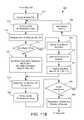
- FIG. 3Ashows an ID generation process with a skip or bypass function performed by the ID generator 234 of FIG. 2B .
- a memory controllersends an ID generation command IDGC, a device type DTsi, an initial ID 0 and others (step 311 ).
- IDGCID generation command
- a device type DTsiinitial ID 0 and others
- the device DVireceives the ID generation command IDGC, the device type DTsi and the IDii (step 312 ).
- the operation of device 1is considered.
- a device order parameter “i”is determined to be “1” (step 312 ).
- operationstarts at a present device DVi (e.g., device 1) (step 313 ).
- the operations of the DT match determination, the ID generation or skip, and the ID assignmentare performed at the device DVi (step 314 ).
- the DT determination and ID generation operationsend at the device DVi (step 315 ).
- the serial output SOi from the present device DViis the serial input SI to the next device DV(i+1) (step 317 ).
- the process by steps 313 - 315is repeated. Such a process is repeated until the last device completes it (YES at step 316 ), all devices in the serial interconnection configuration perform the operations of the device type match determination, the ID generation or skip, and the ID assignment. After the operations are performed at the last device (YES at step 316 ), the normal mode operations will be performed under the control by the memory controller (step 318 ).
- the DT match determination and ID assignment operationsare performed. Then, the given device (or the present device) DVi transmits a combination of the ID generation command IDGC, the device type DTsi and the output IDoi to the next device DV(i+1). If the next device DV(i+1) that received the combined data from the present device DVi is the memory controller 110 , the present device DVi will be determined as the last device in the serial interconnection configuration (YES at step 316 ). This is determined whether the memory controller 110 received the IDGC contained in the combined data. Then, the memory controller 110 recognizes from the received combined data the completion of the DT match determination and ID assignment operations by all devices.
- step 314if there is a device type match between the received DTsi and a device type (i.e., a reference device type DTref) of the device DVi, an ID assignment for the present device and an ID generation for another device will be performed. If there is no match, neither ID assignment nor ID generation will be performed. Details of the operations of the DT match determination and the ID assignment performed at step 314 are shown in FIG. 3B .
- a device typei.e., a reference device type DTref
- a device DViis given and then, the operations of DT match determination and ID assignment process start at the present device DVi (step 313 ).
- the device DVie.g., device 2 receives, from a previous device DV(i ⁇ 1) (e.g., device 1), an input ID, IDii, and the received ID, IDii, is held in the input ID register 440 .
- the device type DTsi for the device type match determinationis received and is held in the input DT register 439 (step 321 ).
- the held DTsiis compared with the reference DT, DTrefi, by the comparator of the DT match detector 446 to determine whether there is a match between the DTsi and the DTref (step 322 ). If the DTsi matches the DTrefi (YES at step 322 ), the DT match signal 249 will be “high” to indicate that the generation of a new ID and the ID assignment are to be performed (step 323 ). In response to the DT match signal 249 being “high”, the n-bit IDii contained in the ID signal 235 is registered or latched in the ID register 231 that has been enabled by the ID write enable signal 233 .
- the received ID, IDiiis assigned to the present device DVi as an ID (step 324 ).
- the ID number or valueis then altered by a “+1” operation (step 325 ) by the adder 450 and the altered or calculated ID is selected by the selector 452 , resulting in a new ID, IDj.
- the DT match signal 249will be “low”. This signal indicates to the present device DVi not to latch the received ID number, IDii, with no adding operation (i.e., no alteration). Thus, the received ID, IDii, is selected by the selector 452 and is kept as a new ID, IDj. (step 327 ).
- the new ID, IDjis fed from the selector 452 to the output ID register 454 .
- the serial ID read from the ID register 454is provided as the new ID, IDj, contained in the output ID signal 281 to the data combiner 267 .
- the IDjis combined with the serial DTsi read from the output DT register 456 and further combined with the ID generation command IDGC by the data combiner 267 .
- the IDjis an output ID, IDoi, of the present device DVi.
- the resultant combination of IDGC, DTsi and IDoiis transmitted to the next device DV(i+1) in the serial interconnection configuration (step 326 ).
- FIG. 4Ashows the devices in the serial interconnection configuration of FIG. 2A , in which the ID generation is performed by the NAND Flash devices.
- FIG. 4Bshows signal timings for the ID generation by the NAND Flash devices of FIG. 4A .
- the data on the SIPcontains the command, DT and ID bits that are fed as the serial input SI 1 to the SIP connection of device 1, 120 - 1 .
- the serial input data fed to the SIP connectionis processed by device controller 230 - 1 of device 1 and the processed data is outputted as the serial output data on the serial output SO 1 through the SOP connection.
- the serial output SO 1is as the serial input Si 2 to neighboring device 2. As such, the serial output of one device is provided to a next device as the serial input.
- the memory controller 110makes the chip select signal /SCS be “low” at time T 1 .
- the memory controller 110sends the reset signal SRST to all devices, so that in response to the internal reset signal 238 provided by the device operation controller 260 , the ID registers 231 of each device is reset.
- the ID register 231holds the reset state (e.g., ‘000’) until an assigned ID is registered therein.
- the memory controller 110provides the serial input SI containing a p-bit ID generation command, IDGC, an m-bit device type DT, DTsi, and an n-bit identifier ID (initial ID 0 ) to device 1, 120 - 1 .
- IDGCp-bit ID generation command
- m-bit device type DTm-bit device type DT
- DTsin-bit identifier ID
- IDinitial ID
- ID 0is a three-bit number ‘000’.
- device 1, 120 - 1performs the operations of the device type match determination, the ID generation or skip, and the ID assignment.
- the device type DTsi sent by the memory controller 110is a DTnd for the NAND Flash device and its DT number or code is ‘00h’ as shown in Table 1.
- the DT match signals 249 at devices 1 , 3 and 5120 - 1 , 120 - 3 and 120 - 5 ) (i.e., NAND Flash devices) become “high” at determination times Tdt 1 , Tdt 3 and Tdt 5 , respectively.
- the DT match signals 249 at devices 2 and 4do not become “high”.
- devices 2 and 4i.e., NOR Flash devices
- devices 1 , 3 and 5In response to the “high” DT match signals 249 , devices 1 , 3 and 5 latch or register the IDs of ‘000’, ‘001’ and ‘010’, respectively, in the ID registers 231 and generate new IDs with +1 operation by the adders 450 .
- steps 324 and 325can be reversed, wherein the “new” ID number (resulting from the “+1” operation) is latched or registered in an ID register of a present device.
- an assigned ID to the deviceis the “new” ID number, instead of the received ID number from the previous device.
- a memory controllermay be configured to address the memory devices in the serial interconnection configuration, according to the IDs generated at each device for the device address recognition in the normal mode operations.
- step 325When each device in the serial interconnection configuration has completed the process as shown in FIG. 3B , all devices with a matching DT number have generated an ID (step 325 ), and all other devices have refrained from generating an ID (step 327 ). To generate IDs for these other devices, the process can be repeated for all devices, wherein the device type DTsi is replaced with another value matching the device type number of some or all of the other devices.
- a first processwith the device type DTnd matching a NAND Flash device, could be completed at all devices, thereby assigning an ID at each NAND Flash device in the serial interconnection configuration.
- a second processwith the device type DTnr matching a NOR Flash device, could be completed at all devices, thereby assigning an ID at each NOR Flash device in the serial interconnection configuration.
- the processmay be further repeated for other device types (e.g., for DRAM devices, SRAM devices) in the serial interconnection configuration.
- each device in the serial interconnection configurationcan be uniquely identified in subsequent values and commands by specifying the ID and DT of that device.
- the device type DTis “00h” (see Table 1.
- devices 1 , 3 and 5120 - 1 , 120 - 3 and 120 - 5 ) determine that the DTsi “matches” the stored DTref (the positive determination) and thus, at step 325 , the +1 operation is performed for generating an altered ID.
- the DT (“01h”)do not match the selected DT (the negative determination at step 322 ) and thus, no +1 operation is performed (step 327 ).
- no ID registrationi.e., no ID latch
- the reset “zero state”is maintained in the ID registers.
- Table 2The resulting latched or registered IDs and generated or bypassed IDs are shown in Table 2.
- FIG. 5Ashows the devices in the serial interconnection configuration shown in FIG. 2A , in which the NOR Flash devices perform the ID generation.
- FIG. 5Bis a timing diagram of the ID generation in the serial interconnection configuration of FIG. 5A .
- devices 1 - 5( 120 - 1 - 120 - 5 ) include the device controllers 230 - 1 - 230 - 5 , respectively. Each of the device controllers provides the DT match determination, the ID generation or skip, and the ID assignment.
- the operations of the serially interconnected devices of FIG. 5Ais similar to those of FIG. 4A .
- FIG. 5Adepicts the operations performed by the serially interconnected devices, wherein the stored DT of the DT number storage/provider 442 is selected for the NOR Flash device, DTnr, the number or code of which is ‘01h’ as shown in Table 1.
- the DT match signals 249 in devices 2 and 4( 120 - 2 and 120 - 4 ) (NOR Flash devices) become “high” at determination times Tdt 2 and Tdt 4 , respectively.
- devices 2 and 4latch or register the IDs ‘000’ and ‘100’ in the ID registers 231 and generate new IDs with +1 operation.
- the DT match signals 249 in devices 1 , 3 and 5do not become “high”.
- the DTsimatches the stored DT of the DT number storage/provider 442 as the reference DTref selected for the NOR Flash device (i.e., “01h” as shown in Table 1).
- devices 2 and 4120 - 2 and 120 - 4 ) determine that the DTsi “matches” the stored DTref, with the results that the +1 operation is performed by the adders 450 to generate a new ID for another device (step 325 ).
- the DTsi(“00h”) does not, however, match the stored DTref (the negative determination at step 322 ), with the results that no +1 operation is performed (i.e., skip or bypass of ID generation (step 327 ).
- Table 3shows t resulting latched or registered IDs and generated or bypassed IDs. In Table 3, “000**” is the reset state.
- Ne.g. 16
- the N-th deviceprovides SON (SO) to the memory controller.
- a general bit structure of the packet bitsis “Packet start+ID generation command IDGC+DT+ID +Packet end”.
- IDGC+DT+ID +Packet endIn the example shown in FIG. 4A , the packets of the serial inputs are given by (ID being “MSB (Most Significant Bit) ⁇ LSB (Least Significant Bit)”:
- the packet bit configuration of the serial input and outputis a packet start, command (IDGC), DT (device type values), ID values and a packet end (optional).
- IDGCpacket start, command
- DTdevice type values
- ID valuesID values
- packet endoptionally
- These information bitsare required in the packets.
- Other information bitsmay be included in the packet depending on the system requirements.
- the number of bits of the information in the packetis varied depending on the system requirements. For example, each of the packet start and end includes four bits.
- the commandincludes any number of bits depending on the system requirements and memory operation modes.
- the DTincludes, for example, eight bits representing the device type value.
- the IDincludes, for example, eight bits representing the ID value.
- the packet bitsare interpreted by the serial packet interpreter 261 and the information of the interpreted packet bits is analyzed by the controller/processor 263 .
- the device type DTsiis a device type DTdm of a DRAM
- only devices 6, 10 and 13perform the ID generation based on the input ID and the other devices skip ID generation, as shown in FIG. 6C .
- the device type DTsiis a device type DTsm of an SRAM
- only devices 7 , 9 and 15perform the ID generation based on the input ID and the other devices skip the ID generation, as shown in FIG. 6D .
- the device type DTsiis a device type DTmm of an MRAM
- only devices 8 and 14perform the ID generation based on the input ID and the other devices skip the ID generation, as shown in FIG. 6E .
- the device type DTsiis a device type DTad of an AND Flash device, it does not match any of the N devices, no ID is generated in the serially interconnected devices, as shown in FIG. 6F . Furthermore, if another type of DTsi is sent the serially interconnected devices, the DTsi will not match any of the devices, with the results that neither ID generation nor ID assignment will be performed.
- Table 4summarizes the input ID, IDi, and the output (generated or skipped) ID, IDo, of each of the devices, in the cases of device types of (1) NAND Flash device (DTnd), (2) NOR Flash device (DTnr), (3) DRAM (DTdm), (4) SRAM (DTsm) and (5) MRAM (DTmm).
- the ID generation based on the +1 operationis performed and the pre-calculated ID is latched as the ID in that device.
- the IDs generated by the specific devicesare indicated in bold.
- FIG. 7Ashows another example of an ID generator that is applied to each of the memory devices serially interconnected as shown in FIG. 1 .
- An ID generator 271 shown in FIG. 7Ais similar to the ID generator 234 of FIG. 2D .
- the same or corresponding elements and components to ones of FIG. 2Dare referenced by the same numerals.
- a DT match detector 390 of the ID generator 271is different from the DT match detector 446 of the ID generator 234 .
- the DT match detector 390provides a “don't care” determination as well as the device type match determination.
- a device type number storage/provider 447is a one-time-programmable (OTP) memory or a programmable memory that can store a device type number or value as a device type reference (DTref) programmed to the device prior to performing the ID generation process.
- the device type number storage/provider 447provides a reference DT signal 448 containing the reference DT, DTref, of m bits to the DT match detector 390 which also receives the DT signal 445 containing the m-bit DTsi from the input DT register 439 .
- the DT determination control signal 221is provided to the DT match detector 390 , so that the determination time Tdti and its active period Tm are defined by the DT determination control signal 221 .
- FIG. 7Bshows details of the DT match detector 390 of FIG. 7A .
- the DT match detector 390includes a DT comparator 461 of m bits and a DT decoder 471 of m bits.
- the DT comparator 461receives the reference DT signal 448 , the DT signal 445 and the DT determination control signal 221 and outputs a comparison result signal 465 to an OR gate 479 .
- the DT decoder 471receives the DT signal 445 and outputs a one-bit decoded signal 475 to the OR gate 479 which in turn provides the DT match signal 249 .
- the DT comparator 461is shown for comparing the m-bit data of the DTsi and the DTref. Accordingly, there are m duplicate comparators to determine whether there is a match between the DTsi and DTref data and output the one-bit determination result data, in response to the DT determination control signal 221 .
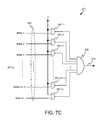
- FIG. 7Cshows details of the DT decoder 471 of FIG. 7B .
- the DT decoder 471includes m input AND gates and one output AND gate. Each of the m input AND gates has two logic inputs. The output AND gate has m logic inputs. The m bits of the device type DTsi, Bdtsi- 1 -Bdtsi-m, contained in the DT signal 445 are fed to one of the logic inputs of AND gates 481 - 1 - 481 - m , respectively. The other logic inputs of the AND gates 481 - 1 - 481 - m receives logic “1” signal commonly (e.g., the other logic inputs being “pulled-up”).
- the logic output signals from the AND gates 481 - 1 - 481 - mare provided to the output AND gate 483 to provide the decoded signal 475 .
- the ID generation performed by the ID generator 271 of FIG. 7Ais shown in FIG. 8 .
- the ID generation command IDGC and the device type (DT), DTsiare provided by the memory controller 110 (step 341 ).
- the memory controller 110sends an initial ID, ID 0 , as the SI format for the ID generation.
- ID 0the SI format for the ID generation.
- “DVi”represents a given device to perform the operations of device type match determination and ID generation.
- a device parameter “i”is determined to be “1” (step 342 ). Then, operation starts at a present device DVi and the operations of the DT match determination and the ID generation are performed at the device DVi.
- the ID generator 271 of the present device DVireceives the IDGC, the DT, DTsi, and the ID, IDii (step 343 ). Then, the DTsi is decoded.
- the “don't care” information bitsare specifically assigned. In this specific example, the bits of the “don't care” DT data are m bits (e.g., eight bits), all of which are “1”. In a case where the “don't care” DT is not decoded from the received DTsi (NO at step 344 ), the DTsi is compared to a reference device type DTref (step 345 ).
- the received IDiiwill be incremented to produce a new ID, IDj (step 346 ). If there is no match at step 345 , the received ID, IDii, will be maintained as a new ID, IDj (step 347 ). Thus, at step 347 , the ID generation is skipped or bypassed. After step 346 or 347 , the new IDj is combined with the DTsi and the IDGC. The IDj is an output ID, IDoi, of the present device DVi. The combined IDGC-DT-ID data is transmitted by the present device DVi to a next device DV(i+1) (step 348 ).
- the present device DViis not the last device (i.e., the N-th device) of the serial interconnection configuration (NO at step 349 )
- the next device DV(i+1)becomes a device DVi and the device ID, IDii, is received thereby (step 350 ).
- the IDis received as the IDii and the ID generation is repeated.
- the ID generation and skip operationsend.
- the determination at step 349is performed in response to the IDGC.
- the present device DVitransmits the combined IDGC-DT-ID to the next device DV(i+1).
- the present device DViwill be determined as the last device in the serial interconnection configuration (YES at step 349 ). This is determined whether the memory controller 110 received the IDGC contained in the combined data.
- device type determination step 345is not performed (i.e., skipped) and always a new ID, IDj, is generated for a next device DV(i+1) (step 346 ).
- a skip functionis performed by the DT match detector 390 .
- device 1receives the initial ID, IDi, as an input ID and device 1 outputs IDo 1 as an output ID.
- Next device 2receives IDo 1 and outputs IDo 2 .
- each of the other devicesreceives an input ID from the previous device and outputs an output ID that is provided to the next device.
- the DTsi contained in the SIis fed to the input DT register 439 which in turn provides the m-bit parallel DTsi to the DT comparator 461 and the DT decoder 471 of the DT match detector 390 .
- the DT decoder 471receives the m-bit device type DTsi contained in the DT signal 445 and decodes it. Only when the DTsi is a pre-determined bit data (e.g., all “1” bits), the decoded signal 475 becomes “high”. Also, the reference device type DTref of m bits is provided by the device type number storage/provider 447 to the DT comparator 461 . In response to the DT determination control signal 221 , the DT comparator 461 compares the m-bit DTsi to the m-bit DTref.
- the DTsiIn a case where the DTsi is the “don't care” device type, the DTsi does not match the DTref, resulting in the comparison result signal 465 from the DT comparator 461 being “low”. Simultaneously, the “don't care” DTsi is decoded by the DT decoder 471 , resulting in the one-bit decoded signal 475 from the DT decoder 471 being “high” for time period Tm. Thus, the DT match signal 249 from the OR gate 479 becomes “high” and the selector 452 selects the calculation signal 451 having a +1 operation value. These operations are depicted in step 346 in FIG. 8 .
- the decoded signal 475 from the DT decoder 471is “low”. Furthermore, if the DTsi does not match the DTref, the comparison result signal 465 from the DT comparator 461 will be “low”, in response to the DT determination control signal 221 . If the DTsi matches the DTref, the comparison result signal 465 will be “high” for time period Tm, with the result that the DT match signal 249 is “high” and the “+1” operation value is selected by the selector 452 . These operations are depicted in steps 344 - 347 in FIG. 8 . Therefore, the process shown in FIG. 8 can generate consecutive IDs for all devices, regardless of devices types in the serial interconnection configuration.
- the device type IDii for the present deviceis registered in the ID register 231 .
- Table 6shows the latched IDs in and generated IDs by all devices.
- FIG. 10shows an example structure of an operation controller/processor included in the memory controller 110 of FIG. 1 .
- an operation controller/processor 510includes an operation/process controller 512 that provides the clock signal SCLK to an ID recognizer 514 .
- the operation/process controller 512provides a device type (DT) signal 516 containing a device type DTsi-k to a data compiler 518 .
- the ID recognizer 514receives the ID signal containing the IDo 16 - k from the last device (i.e., device 16) of the serial interconnection configuration.
- the ID recognizer 514provides an ID signal 521 containing the ID, IDo 16 - k , to the data compiler 518 .
- the data compiler 518provides a memory 524 with compiled data from the provided DTsi-k and IDo 16 - k .
- the memory 524stores compiled data as a table including the device types and the last IDs.
- kis an operation repetition parameter of repeated DT recognition and varies from 1 to M, M being an integer greater than 1.
- FIG. 11Ashows an ID generation method performed by the devices shown in FIG. 1 .
- FIG. 11Bshows part of the method shown in FIG. 11A .
- the ID generationis performed by the ID generator shown in FIG. 7A .
- FIG. 12shows another example of a protocol conducted in the devices shown in FIG. 1 .
- the operation repetition parameter kis assigned a value of 1 (step 351 ).
- the memory controller 110(the operation controller/processor 510 ) sends an ID generation command IDGC, a device type DT, DTsi-k, and an initial ID, ID 0 k , as a packet to device 1 (step 352 ).
- the device DVie.g., device 2 receives, from a previous device DV(i ⁇ 1) (e.g., device 1), a device ID, IDii, and the received ID is held in the input ID register 440 (step 373 ). Then, the device type match determination occurs.
- the DT clock generator 441 of the ID generator 271generates the DT register clocks in response to the clock signal SCLK and the received DTsi-k is shifted into the input DT register 439 .
- the device type DTsi-kis held in the input DT register 439 of the present device DVi.
- the DT comparator 461compares the held DTsi-k to the reference DT, DTrefi, associated with the present device (step 374 ). If the values or numbers match between the DTsi-k and the DTrefi (YES at step 374 ), there will be provided a match indication between the DTsi-k and the DTrefi (step 375 ).
- the DT match signal 249will be “high”.
- This signalindicates to the present device to store the received device ID, IDii, (step 376 ), thereby assigning or establishing the device ID for the present device, DVi.
- the ID number or valueis altered by a “+1” operation (step 377 ), resulting in a new ID, IDj.
- the DT match signal 249indicates to the present device neither to store the ID, nor conducting an ID alteration (step 378 ).
- the new ID, IDjis converted to a serial output signal (step 379 ) for transmission to the next device DV(i+1) (e.g., device 3 ) in the serial interconnection configuration.
- the next device DV(i+1)receives the ID number, IDii.
- the ID generation process at the device DViends (step 380 ). If the device DVi is not the last device (i.e., device N) (NO at step 381 ), a next device DV(i+1) will be given (step 382 ) and the process at steps 372 - 380 will be repeated at that device DV(i+1).
- the ID recognizer 514 of the operation controller/processor 510recognizes the IDo 16 - k received from the last device (i.e., device N), at the time of receiving the IDGC and the DTsi-k (step 383 ) and moves to step 354 .
- the number of the devices of the provided device type DTsi-kis recognized by the data compiler 518 (step 383 ). Such operations of the ID generation and the last ID recognition are repeated with reference to the operation repetition parameter k being 1 to M (i.e., DTsi 1 to DTsiM).
- the data compiler 518Upon receipt of the DTsi-k from the operation/process controller 512 and the IDo 16 - k from the ID recognizer 514 , the data compiler 518 compiles data with regard to the device type DTsi-k, the last ID and the number of devices having the device type DTsi-k. The compiled data is stored in the memory 524 as a table.
- the device types DTsi for the device type match searchare the DTnd for NAND Flash devices, the DTnr for NAND Flash devices, the DTdm for DRAM devices, the DTsm for SRAM devices, the DTmm for MRAM devices and the “don't care” for every type memory device.
- the data fed by the data compiler 518is stored in the memory 524 .
- Table 7shows compiled data.
- the memory controllercan recognize the number of the device with regard to the specific DT.
- the DT match detector 390 of FIG. 7Aincludes the DT decoder 471 that detects only when all bits of the DTsi are “1”,
- the DT decoder 471can be replaced with an m-bit comparator that detects pre-defined data or information of the “don't care” device type DTdc.
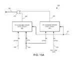
- FIG. 13Ashows another example of a DT match detector shown in FIG. 7A .
- a DT match detector 530 shown in FIG. 13Ais similar to the DT match detector 390 of FIG. 7B .
- a differenceis that the DT match detector 530 includes a DT comparator 531 , instead of the DT decoder 471 .
- the DT comparator 531is similar to the m-bit DT comparator 461 .
- the DT comparator 531is also an m-bit comparator.
- the DT comparator 531receives the DT signal 445 containing the m-bit parallel DTsi, a “don't care” code signal 533 containing a “don't care” device type DTdc from a code source (not shown) and the DT determination control signal 221 .
- the DT comparator 531outputs a comparison result signal 535 to the OR gate 479 .
- FIG. 13BThe ID generation performed by the ID generator 271 of FIG. 7A including the DT match detector 530 of FIG. 13A is shown in FIG. 13B .
- the ID generation process shown in FIG. 13Bis similar to that of FIG. 8 .
- a differenceis that the process shown in FIG. 13B includes a “don't care” determination step (step 394 ), instead of the “don't care” decoding step (step 344 ) of FIG. 8 .
- the ID generator 271 of the present device DVireceives the IDGC, the DT, DTsi, and the ID, IDii (step 343 ). Then, the DTsi is compared to a “don't care” device type DTdc by the DT comparator 531 (step 394 ). In a case of the DTsi not being “don't care”, the received DTsi is compared to a reference device type DTref (step 345 ). If the DTsi matches the DTref, the received ID will be incremented to produce a new ID, IDj (step 346 ).
- the received ID, IDiiwill be maintained as a new IDj (step 347 ).
- the ID generationis skipped or bypassed.
- the new IDis outputted by the ID generator of the device DVi to a next device DV(i+1) (step 348 ).
- device type determination step 345is not performed and a new ID is always generated for a next device DV(i+1) (step 346 ).
- the “don't care” codecan be defined by any of bit combinations.
- a memory controllercan send such a pre-defined code as a device type DTsi as a serial input form.
- the latched ID in the ID register 231 of a deviceis the ID previously generated in the device wherein the device type DT matches the reference device type DTref thereof.
- the assigned ID to the present deviceis the ID generated by the ID generator 234 of another device and received by the present device.
- a devicelatches an ID generated thereby before or simultaneously the generated ID is transmitted to a next device.
- the stored and assigned ID to a deviceis the ID generated by the device when the device type DT matches the reference device type DTref thereof.
- FIG. 14An ID generator shown in FIG. 14 is similar to the ID generators 234 and 271 of FIGS. 2D and 7A . A difference is that in an ID generator 273 of FIG. 14 , the added ID (IDii+1) by the adder 450 is provided to the ID register 231 for registration or latch, instead of the non-calculated (non-altered) ID from the input ID register 440 .
- the assigned IDis one generated by that device, not one generated by the previous or the other device. Therefore, the latched or registered IDs in the devices are different from ones shown in Tables 2 and 3.
- a DT match detector 541is similar to the DT match detector 446 of FIG. 2D or the DT match detector 390 of FIG. 7A .
- a device type number storage/provider 542provides a reference DT signal 543 containing a reference DTref.
- the comparator of the DT match detector 541compares the received DTsi to the reference DTref or the reference DTref and the “don't care” device type DTdc to detect a device type match.
- the DT match signal 249is provided.
- Tables 4 and 5show the latched or registered IDs and the generated or bypassed IDs in the devices of the serial interconnection configuration shown in FIG. 2A with the ID generator as shown in FIG. 14 , in the cases where the device types provided by the memory controller are the DTnd and DTnr for NAND and NOR Flash devices, respectively.
- “000**”is the reset state, not a latched ID.
- the latched IDsare different.
- Table 10shows the latched IDs in and generated IDs by all devices.
- FIG. 15shows another example of the ID generation.
- an ID generator 275is similar to the ID generators 234 and 271 of FIGS. 2D and 7A .
- a differenceis that the ID generator 275 includes a subtractor 550 , instated of an adder.
- a DT match detector 545is similar to the DT match detector 446 of FIG. 2D or the DT match detector 390 of FIG. 7A .
- a device type number storage/provider 546provides a reference DT signal 547 containing a reference DTref.
- the comparator of the DT match detector 545compares the received DTsi to the reference DTref or the reference DTref and the “don't care” device type DTdc to detect a device type match.
- the DT match signal 249is provided.
- the subtractor 550subtracts one from the received IDi and the subtracted ID will be provided as a new ID, IDj, contained in subtraction output signal 551 , if the received DTsi matches the reference DTref,
- ID generator 275With the ID generator 275 , consecutive IDs from high to low are generated. If the initial ID number provided by a memory controller is Q (an integer), IDs will be generated in consecutive numbers from (Q-1) to low by the devices. In a case of Q being 16, the generated ID number is a consecutive number from 15 to 0. Table 11 shows the latched IDs in and generated IDs by all devices wherein the “don't care” device type DTdc is provided by the memory controller 110 .
- Each of the subtractor 550 of FIG. 15 and the adder 450 of FIG. 2Dperforms an arithmetic operation for calculating an ID to be newly generated for another device.
- the arithmetic operationcan be achieved by increment or decrement by one or any other number or value.
- the increment or decrement by oneis an example for an ID alteration.
- FIG. 16shows another example of the ID generator.
- An ID generator 277 shown in FIG. 16is similar to the ID generator 275 of FIG. 15 . A difference is that the ID generator 277 provides a subtracted ID, IDii ⁇ 1 to the ID register 231 wherein the ID is latched or registered in accordance with the DT match signal 249 .
- a DT match detector 552is similar to the DT match detector 446 of FIG. 2D or the DT match detector 390 of FIG. 7A .
- a device type number storage/provider 553provides a reference DT signal 554 containing a reference DTref.
- the comparator of the DT match detector 552compares the received DTsi to the reference DTref or the reference DTref and the “don't care” device type DTdc to detect a device type match.
- the DT match signal 249is provided.
- Table 12shows the latched IDs in and generated IDs by all devices wherein the “don't care” device type DTdc is provided.
- FIG. 17Ashows a machine-readable medium storing commands and instructions that can be used for the devices 120 - 1 - 120 - 16 of FIG. 1 .
- a computer-readable medium 571e.g., a non-volatile memory
- instruction codes 572is provided to a reader 573 which in turn reads the instruction codes 572 .
- the read codesare provided to a memory 574 and stored therein. If the memory 574 is included in the device 120 - i , its device operation controller 260 can process the codes stored in the memory 574 and perform the functions defined by the instruction codes 572 .
- the device operation controller 260can execute the commands and instructions to perform the methods.
- FIG. 17Bshows a machine-readable medium storing commands and instructions that can be used for the memory controller 110 of FIG. 1 .
- a computer-readable medium 576e.g., a non-volatile memory
- the reader 578reads the instruction codes 577 and the read codes are provided to a memory 579 and stored therein. If the memory 579 is included in the memory controller 110 , the operation controller/processor 510 of which can process the codes stored in the memory 579 and perform the functions defined by the instruction codes 577 .
- the operation controller/processor 510can execute the commands and instructions to perform the methods.
- the present inventionis applicable to a system including a plurality of devices in a serial interconnection configuration operating to generate an ID at each device employing an example of ID generation logic for dual links.
- serial inputs SI 0 and SI 1are fed into serial input port connections SIP 0 and SIP 1 of a device and serial outputs SO 0 and SO 1 are provided from serial output port connections SOP 0 and SOP 1 of that device.
- the transferring of the serial inputs SI 0 , SI 1 and the serial outputs SO 0 , SO 1is separately controlled. Any serial input pin and one control pin can have the same functionality.
- an ID generation logicmay be possible for multiple links wherein a plurality of devices having multiple ports is interconnected.
- the above-described embodimentsmay operate with either of a single data rate (SDR) interface or a double data rate (DDR) interface.
- SDRsingle data rate
- DDRdouble data rate
- the bit structure of the ID stored in the ID register 231 of the devices 120 - i and transmitted in a packetis “MSB ⁇ LSB”.
- the bit structure of each of other datae.g., “Packet Start”, “IDGC”, “DT”, “Packet End” contained in the packet is also “MSB ⁇ LSB”.
- the bit structure of each data contained in a packetcan be “LSB ⁇ MSB” and the ID bits of “LSB ⁇ MSB” can be stored in the ID register 231 .
- the ID generation command IDGC, the device type DT and the device identifier IDare transmitted as a packet.
- data on the IDGC, DT and IDcan be transmitted as a group by a way other than a packet.
- the operationhas been described based on the active “high” signals for the purpose of simplicity.
- the circuits of any blocksmay be designed to perform the operation based on the “low” active signals, in accordance with a design preference.
- the device elements and circuitsare connected to each other as shown in the figures, for the sake of simplicity.
- devices, elements, circuits, etc.may be connected directly to each other.
- devices, elements, circuits etc.may be connected indirectly to each other through other devices, elements, circuits, etc., necessary for operation of the apparatus.
- the circuit elements and devicesare directly or indirectly coupled with or connected to each other.
- the embodiments described aboveare directed to systems including memory devices.
- the technique described abovecan be applied to systems including other semiconductor devices, such as, for example, data processing devices, which are distinguishable in accordance with predetermined data or information on their characteristics or types.
- Such systemscan be included by electronic equipment or products.
- ID generators or producers, the controllers, the processors and the other device elements and the memory controllersmay be achieved by hardware or software.
Landscapes
- Information Transfer Systems (AREA)
Abstract
Description
| TABLE 1 | ||||||||||
| Bit | Bit | Bit | Bit | Bit | Bit | Bit | Bit | |||
| HEX | 7 | 6 | 5 | 4 | 3 | 2 | 1 | 0 | ||
| 00h | 0 | 0 | 0 | 0 | 0 | 0 | 0 | 0 | ||
| (DTnd) | ||||||||||
| NOR | 01h | 0 | 0 | 0 | 0 | 0 | 0 | 0 | 1 | |
| (DTnr) | ||||||||||
| AND | 02h | 0 | 0 | 0 | 0 | 0 | 0 | 1 | 0 | |
| (DTad) | ||||||||||
| 03h | 0 | 0 | 0 | 0 | 0 | 0 | 1 | 1 | ||
| (DTdm) | ||||||||||
| 04h | 0 | 0 | 0 | 0 | 0 | 1 | 0 | 0 | ||
| (DTsm) | ||||||||||
| 05h | 0 | 0 | 0 | 0 | 0 | 1 | 0 | 1 | ||
| (DTmm) | ||||||||||
| — | — | — | — | — | — | — | — | — | — | |
| — | — | — | — | — | — | — | — | — | — | |
| — | — | — | — | — | — | — | — | — | — | |
| Not Used* | 1 | 1 | 1 | 1 | 1 | 1 | 1 | 1 | ||
| TABLE 2 | |||||
| DT Number | |||||
| or Value | Latched or | Generated or | |||
| Device | Device Type | (DTref) | Registered ID | Bypassed ID | |
| 220-1 | NAND Flash | 00h | 000 | 001 | |
| 220-2 | NOR | 01h | 000** | 001 | |
| 220-3 | NAND Flash | 00h | 001 | 010 | |
| 220-4 | NOR | 01h | 000** | 010 | |
| 220-5 | NAND Flash | 00h | 010 | 011 | |
| TABLE 3 | |||||
| DT Number | |||||
| or Value | Latched or | Generated or | |||
| Device | Device Type | (DTref) | Registered ID | Bypassed ID | |
| 220-1 | NAND Flash | 00h | 000** | 000 | |
| 220-2 | NOR | 01h | 000 | 001 | |
| 220-3 | NAND Flash | 00h | 000** | 001 | |
| 220-4 | NOR | 01h | 001 | 010 | |
| 220-5 | NAND Flash | 00h | 000** | 010 | |
- SI1: Packet including the ID0=Packet Start+IDGC+DT+‘000’+Packet End
- SI2: Packet including the ID1=Packet Start+IDGC+DT+‘001’+Packet End
- SI3: Ibid
- SI4: Packet including the ID2=Packet Start+IDGC+DT+‘010’+Packet End
- SI5: Ibid
- SO5: Packet including the ID3=Packet Start+IDGC+DT+‘011’+Packet End
| TABLE 4 | ||||||
| Number | Memory | (1) DTnd | (2) DTnr | (3) DTdm | (4) DTsm | (5) DTmm |
| DV# | Device Type | IDi | IDo | IDi | IDo | ID | IDo | IDi | IDi | IDo | ||
| 1 | 0 | 1 | 0 | 0 | 0 | 0 | 0 | 0 | 0 | 0 | |
| 2 | NOR | 1 | 1 | 0 | 1 | 0 | 0 | 0 | 0 | 0 | 0 |
| 3 | 1 | 2 | 1 | 1 | 0 | 0 | 0 | 0 | 0 | 0 | |
| 4 | NOR | 2 | 2 | 1 | 2 | 0 | 0 | 0 | 0 | 0 | 0 |
| 5 | 2 | 3 | 2 | 2 | 0 | 0 | 0 | 0 | 0 | 0 | |
| 6 | 3 | 3 | 2 | 2 | 0 | 1 | 0 | 0 | 0 | 0 | |
| 7 | 3 | 3 | 2 | 2 | 1 | 1 | 0 | 1 | 0 | 0 | |
| 8 | 3 | 3 | 2 | 2 | 1 | 1 | 1 | 1 | 0 | 1 | |
| 9 | 3 | 3 | 2 | 2 | 1 | 1 | 1 | 2 | 1 | 1 | |
| 10 | 3 | 3 | 2 | 2 | 1 | 2 | 2 | 2 | 1 | 1 | |
| 11 | NOR | 3 | 3 | 2 | 3 | 2 | 2 | 2 | 2 | 1 | 1 |
| 12 | 3 | 4 | 3 | 3 | 2 | 2 | 2 | 2 | 1 | 1 | |
| 13 | 4 | 4 | 3 | 3 | 2 | 3 | 2 | 2 | 1 | 1 | |
| 14 | 4 | 4 | 3 | 3 | 3 | 3 | 2 | 2 | 1 | 2 | |
| 15 | 4 | 4 | 3 | 3 | 3 | 3 | 2 | 3 | 2 | 2 | |
| 16 | 4 | 5 | 3 | 3 | 3 | 3 | 3 | 3 | 2 | 2 | |
| TABLE 5 | ||
| Device Number DV# | Memory Device Type | Latched or |
| 1 | 0 | |
| 2 | NOR | 0 |
| 3 | 1 | |
| 4 | NOR | 1 |
| 5 | 2 | |
| 6 | 0 | |
| 7 | 0 | |
| 8 | 0 | |
| 9 | 1 | |
| 10 | 1 | |
| 11 | NOR | 2 |
| 12 | 3 | |
| 13 | 2 | |
| 14 | 1 | |
| 15 | 2 | |
| 16 | 4 | |
| TABLE 6 | |||||
| Device | Memory | Latched ID | Generated | ||
| Number DV# | Device Type | (Number) | ID (Number) | ||
| 1 | 0 | 1 | |||
| 2 | NOR | 1 | 2 | ||
| 3 | 2 | 3 | |||
| 4 | NOR | 3 | 4 | ||
| 5 | 4 | 5 | |||
| 6 | 5 | 6 | |||
| 7 | 6 | 7 | |||
| 8 | 7 | 8 | |||
| 9 | 8 | 9 | |||
| 10 | 9 | 10 | |||
| 11 | NOR | 10 | 11 | ||
| 12 | 11 | 12 | |||
| 13 | 12 | 13 | |||
| 14 | 13 | 14 | |||
| 15 | 14 | 15 | |||
| 16 | 15 | 16 | |||
| TABLE 7 | ||||
| Device Type | Last ID | Number of | ||
| K | (DTsi) | (IDo16) | DT's | |
| 1 | NAND Flash (DTnd) | 5 | ||
| 2 | NOR Flash (DTnr) | 3 | ||
| 3 | DRAM (DTdm) | 3 | ||
| 4 | SRAM (DTsm) | 3 | ||
| 5 | MRAM (DTmm) | 2 | ||
| 6 | AND Flash (DTad) | 0 | ||
| 7 | Don't Care (DTdc) | | 16 | |
| — | — | — | — | |
| — | — | — | — | |
| — | — | — | — | |
| — | — | — | — | |
| TABLE 8 | |||||
| DT Number or | Latched or | Generated or | |||
| Device | Device Type | Value | Registered ID | Bypassed ID | |
| 220-1 | NAND Flash | 00h | 001 | 001 | |
| 220-2 | NOR | 01h | 000** | 001 | |
| 220-3 | NAND Flash | 00h | 010 | 010 | |
| 220-4 | NOR | 01h | 000** | 010 | |
| 220-5 | NAND Flash | 00h | 011 | 011 | |
| TABLE 9 | |||||
| DT Number or | Latched or | Generated or | |||
| Device | Device Type | Value | Registered ID | Bypassed ID | |
| 220-1 | NAND Flash | 00h | 000** | 000 | |
| 220-2 | NOR | 01h | 001 | 001 | |
| 220-3 | NAND Flash | 00h | 000** | 001 | |
| 220-4 | NOR | 01h | 010 | 010 | |
| 220-5 | NAND Flash | 00h | 000** | 010 | |
| TABLE 10 | ||||
| Device | Memory | Latched ID | Generated ID | |
| Number DV# | Device Type | (Number) | (Number) | |
| 1 | 1 | 1 | ||
| 2 | NOR | 2 | 2 | |
| 3 | 3 | 3 | ||
| 4 | NOR | 4 | 4 | |
| 5 | 5 | 5 | ||
| 6 | 6 | 6 | ||
| 7 | 7 | 7 | ||
| 8 | 8 | 8 | ||
| 9 | 9 | 9 | ||
| 10 | 10 | 10 | ||
| 11 | NOR | 11 | 11 | |
| 12 | 12 | 12 | ||
| 13 | 13 | 13 | ||
| 14 | 14 | 14 | ||
| 15 | 15 | 15 | ||
| 16 | 16 | 16 | ||
| TABLE 11 | |||||
| Device | Memory | Latched | Generated | ||
| Number DV# | Device Type | ID (Number) | ID (Number) | ||
| 1 | NAND Flash | Q | Q-1 | ||
| 2 | NOR Flash | Q-1 | Q-2 | ||
| 3 | NAND Flash | Q-2 | Q-3 | ||
| 4 | NOR Flash | Q-3 | Q-4 | ||
| 5 | NAND Flash | Q-4 | Q-5 | ||
| 6 | DRAM | Q-5 | Q-6 | ||
| 7 | SRAM | Q-6 | Q-7 | ||
| 8 | MRAM | Q-7 | Q-8 | ||
| 9 | SRAM | Q-8 | Q-9 | ||
| 10 | DRAM | Q-9 | Q-10 | ||
| 11 | NOR Flash | Q-10 | Q-11 | ||
| 12 | NAND Flash | Q-11 | Q-12 | ||
| 13 | DRAM | Q-12 | Q-13 | ||
| 14 | MRAM | Q-13 | Q-14 | ||
| 15 | SRAM | Q-14 | Q-15 | ||
| 16 | NAND Flash | Q-15 | Q-16 | ||
| TABLE 12 | |||||
| Device | Memory | Latched | Generated | ||
| Number DV# | Device Type | ID (Number) | ID (Number) | ||
| 1 | NAND Flash | Q-1 | Q-1 | ||
| 2 | NOR Flash | Q-2 | Q-2 | ||
| 3 | NAND Flash | Q-3 | Q-3 | ||
| 4 | NOR Flash | Q-4 | Q-4 | ||
| 5 | NAND Flash | Q-5 | Q-5 | ||
| 6 | DRAM | Q-6 | Q-6 | ||
| 7 | SRAM | Q-7 | Q-7 | ||
| 8 | MRAM | Q-8 | Q-8 | ||
| 9 | SRAM | Q-9 | Q-9 | ||
| 10 | DRAM | Q-10 | Q-10 | ||
| 11 | NOR Flash | Q-11 | Q-11 | ||
| 12 | NAND Flash | Q-12 | Q-12 | ||
| 13 | DRAM | Q-13 | Q-13 | ||
| 14 | MRAM | Q-14 | Q-14 | ||
| 15 | SRAM | Q-15 | Q-15 | ||
| 16 | NAND Flash | Q-16 | Q-16 | ||
Claims (10)
Priority Applications (1)
| Application Number | Priority Date | Filing Date | Title |
|---|---|---|---|
| US12/892,215US8195839B2 (en) | 2006-12-06 | 2010-09-28 | Apparatus and method for producing identifiers regardless of mixed device type in a serial interconnection |
Applications Claiming Priority (4)
| Application Number | Priority Date | Filing Date | Title |
|---|---|---|---|
| US86877306P | 2006-12-06 | 2006-12-06 | |
| US88957207P | 2007-02-13 | 2007-02-13 | |
| US11/692,446US7853727B2 (en) | 2006-12-06 | 2007-03-28 | Apparatus and method for producing identifiers regardless of mixed device type in a serial interconnection |
| US12/892,215US8195839B2 (en) | 2006-12-06 | 2010-09-28 | Apparatus and method for producing identifiers regardless of mixed device type in a serial interconnection |
Related Parent Applications (1)
| Application Number | Title | Priority Date | Filing Date |
|---|---|---|---|
| US11/692,446ContinuationUS7853727B2 (en) | 2006-12-06 | 2007-03-28 | Apparatus and method for producing identifiers regardless of mixed device type in a serial interconnection |
Publications (2)
| Publication Number | Publication Date |
|---|---|
| US20110016236A1 US20110016236A1 (en) | 2011-01-20 |
| US8195839B2true US8195839B2 (en) | 2012-06-05 |
Family
ID=39685719
Family Applications (2)
| Application Number | Title | Priority Date | Filing Date |
|---|---|---|---|
| US11/692,446Expired - Fee RelatedUS7853727B2 (en) | 2006-12-06 | 2007-03-28 | Apparatus and method for producing identifiers regardless of mixed device type in a serial interconnection |
| US12/892,215Expired - Fee RelatedUS8195839B2 (en) | 2006-12-06 | 2010-09-28 | Apparatus and method for producing identifiers regardless of mixed device type in a serial interconnection |
Family Applications Before (1)
| Application Number | Title | Priority Date | Filing Date |
|---|---|---|---|
| US11/692,446Expired - Fee RelatedUS7853727B2 (en) | 2006-12-06 | 2007-03-28 | Apparatus and method for producing identifiers regardless of mixed device type in a serial interconnection |
Country Status (2)
| Country | Link |
|---|---|
| US (2) | US7853727B2 (en) |
| TW (1) | TWI476779B (en) |
Cited By (1)
| Publication number | Priority date | Publication date | Assignee | Title |
|---|---|---|---|---|
| US20120072626A1 (en)* | 2010-09-22 | 2012-03-22 | Microsoft Corporation | Automatic Addressing Protocol for a Shared Bus |
Families Citing this family (48)
| Publication number | Priority date | Publication date | Assignee | Title |
|---|---|---|---|---|
| US8331361B2 (en)* | 2006-12-06 | 2012-12-11 | Mosaid Technologies Incorporated | Apparatus and method for producing device identifiers for serially interconnected devices of mixed type |
| CN101617371B (en) | 2007-02-16 | 2014-03-26 | 莫塞德技术公司 | Non-volatile semiconductor memory with multiple external power supplies |
| US8122202B2 (en) | 2007-02-16 | 2012-02-21 | Peter Gillingham | Reduced pin count interface |
| US8131913B2 (en) | 2008-02-04 | 2012-03-06 | Mosaid Technologies Incorporated | Selective broadcasting of data in series connected devices |
| US8713697B2 (en) | 2008-07-09 | 2014-04-29 | Lennox Manufacturing, Inc. | Apparatus and method for storing event information for an HVAC system |
| US7957173B2 (en) | 2008-10-14 | 2011-06-07 | Mosaid Technologies Incorporated | Composite memory having a bridging device for connecting discrete memory devices to a system |
| US8527096B2 (en) | 2008-10-24 | 2013-09-03 | Lennox Industries Inc. | Programmable controller and a user interface for same |
| US8600559B2 (en) | 2008-10-27 | 2013-12-03 | Lennox Industries Inc. | Method of controlling equipment in a heating, ventilation and air conditioning network |
| US8600558B2 (en) | 2008-10-27 | 2013-12-03 | Lennox Industries Inc. | System recovery in a heating, ventilation and air conditioning network |
| US8463442B2 (en) | 2008-10-27 | 2013-06-11 | Lennox Industries, Inc. | Alarm and diagnostics system and method for a distributed architecture heating, ventilation and air conditioning network |
| US8442693B2 (en) | 2008-10-27 | 2013-05-14 | Lennox Industries, Inc. | System and method of use for a user interface dashboard of a heating, ventilation and air conditioning network |
| US8564400B2 (en) | 2008-10-27 | 2013-10-22 | Lennox Industries, Inc. | Communication protocol system and method for a distributed-architecture heating, ventilation and air conditioning network |
| US8744629B2 (en) | 2008-10-27 | 2014-06-03 | Lennox Industries Inc. | System and method of use for a user interface dashboard of a heating, ventilation and air conditioning network |
| US8452456B2 (en) | 2008-10-27 | 2013-05-28 | Lennox Industries Inc. | System and method of use for a user interface dashboard of a heating, ventilation and air conditioning network |
| US8788100B2 (en) | 2008-10-27 | 2014-07-22 | Lennox Industries Inc. | System and method for zoning a distributed-architecture heating, ventilation and air conditioning network |
| US8463443B2 (en) | 2008-10-27 | 2013-06-11 | Lennox Industries, Inc. | Memory recovery scheme and data structure in a heating, ventilation and air conditioning network |
| US8655491B2 (en) | 2008-10-27 | 2014-02-18 | Lennox Industries Inc. | Alarm and diagnostics system and method for a distributed architecture heating, ventilation and air conditioning network |
| US8543243B2 (en) | 2008-10-27 | 2013-09-24 | Lennox Industries, Inc. | System and method of use for a user interface dashboard of a heating, ventilation and air conditioning network |
| US8798796B2 (en) | 2008-10-27 | 2014-08-05 | Lennox Industries Inc. | General control techniques in a heating, ventilation and air conditioning network |
| US8774210B2 (en) | 2008-10-27 | 2014-07-08 | Lennox Industries, Inc. | Communication protocol system and method for a distributed-architecture heating, ventilation and air conditioning network |
| US8977794B2 (en) | 2008-10-27 | 2015-03-10 | Lennox Industries, Inc. | Communication protocol system and method for a distributed-architecture heating, ventilation and air conditioning network |
| US9432208B2 (en) | 2008-10-27 | 2016-08-30 | Lennox Industries Inc. | Device abstraction system and method for a distributed architecture heating, ventilation and air conditioning system |
| US9651925B2 (en) | 2008-10-27 | 2017-05-16 | Lennox Industries Inc. | System and method for zoning a distributed-architecture heating, ventilation and air conditioning network |
| US8452906B2 (en) | 2008-10-27 | 2013-05-28 | Lennox Industries, Inc. | Communication protocol system and method for a distributed-architecture heating, ventilation and air conditioning network |
| US8655490B2 (en) | 2008-10-27 | 2014-02-18 | Lennox Industries, Inc. | System and method of use for a user interface dashboard of a heating, ventilation and air conditioning network |
| US8615326B2 (en) | 2008-10-27 | 2013-12-24 | Lennox Industries Inc. | System and method of use for a user interface dashboard of a heating, ventilation and air conditioning network |
| US8994539B2 (en) | 2008-10-27 | 2015-03-31 | Lennox Industries, Inc. | Alarm and diagnostics system and method for a distributed-architecture heating, ventilation and air conditioning network |
| US8295981B2 (en) | 2008-10-27 | 2012-10-23 | Lennox Industries Inc. | Device commissioning in a heating, ventilation and air conditioning network |
| US8433446B2 (en) | 2008-10-27 | 2013-04-30 | Lennox Industries, Inc. | Alarm and diagnostics system and method for a distributed-architecture heating, ventilation and air conditioning network |
| US8762666B2 (en) | 2008-10-27 | 2014-06-24 | Lennox Industries, Inc. | Backup and restoration of operation control data in a heating, ventilation and air conditioning network |
| US8548630B2 (en) | 2008-10-27 | 2013-10-01 | Lennox Industries, Inc. | Alarm and diagnostics system and method for a distributed-architecture heating, ventilation and air conditioning network |
| US8437877B2 (en) | 2008-10-27 | 2013-05-07 | Lennox Industries Inc. | System recovery in a heating, ventilation and air conditioning network |
| US9678486B2 (en) | 2008-10-27 | 2017-06-13 | Lennox Industries Inc. | Device abstraction system and method for a distributed-architecture heating, ventilation and air conditioning system |
| US8437878B2 (en) | 2008-10-27 | 2013-05-07 | Lennox Industries Inc. | Alarm and diagnostics system and method for a distributed architecture heating, ventilation and air conditioning network |
| US8661165B2 (en)* | 2008-10-27 | 2014-02-25 | Lennox Industries, Inc. | Device abstraction system and method for a distributed architecture heating, ventilation and air conditioning system |
| US8725298B2 (en) | 2008-10-27 | 2014-05-13 | Lennox Industries, Inc. | Alarm and diagnostics system and method for a distributed architecture heating, ventilation and conditioning network |
| US8892797B2 (en) | 2008-10-27 | 2014-11-18 | Lennox Industries Inc. | Communication protocol system and method for a distributed-architecture heating, ventilation and air conditioning network |
| US9325517B2 (en) | 2008-10-27 | 2016-04-26 | Lennox Industries Inc. | Device abstraction system and method for a distributed-architecture heating, ventilation and air conditioning system |
| US8694164B2 (en) | 2008-10-27 | 2014-04-08 | Lennox Industries, Inc. | Interactive user guidance interface for a heating, ventilation and air conditioning system |
| US8874815B2 (en) | 2008-10-27 | 2014-10-28 | Lennox Industries, Inc. | Communication protocol system and method for a distributed architecture heating, ventilation and air conditioning network |
| US9632490B2 (en) | 2008-10-27 | 2017-04-25 | Lennox Industries Inc. | System and method for zoning a distributed architecture heating, ventilation and air conditioning network |
| US8855825B2 (en) | 2008-10-27 | 2014-10-07 | Lennox Industries Inc. | Device abstraction system and method for a distributed-architecture heating, ventilation and air conditioning system |
| US8560125B2 (en) | 2008-10-27 | 2013-10-15 | Lennox Industries | Communication protocol system and method for a distributed-architecture heating, ventilation and air conditioning network |
| US8802981B2 (en) | 2008-10-27 | 2014-08-12 | Lennox Industries Inc. | Flush wall mount thermostat and in-set mounting plate for a heating, ventilation and air conditioning system |
| US8549209B2 (en) | 2008-11-04 | 2013-10-01 | Mosaid Technologies Incorporated | Bridging device having a configurable virtual page size |
| DE112010002750T5 (en) | 2009-06-29 | 2013-01-31 | Mosaid Technologies Incorporated | Bridge device with a clock domain with configurable frequency |
| US9479344B2 (en)* | 2011-09-16 | 2016-10-25 | Telecommunication Systems, Inc. | Anonymous voice conversation |
| WO2016145328A2 (en)* | 2015-03-11 | 2016-09-15 | Rambus Inc. | High performance non-volatile memory module |
Citations (99)
| Publication number | Priority date | Publication date | Assignee | Title |
|---|---|---|---|---|
| US4174536A (en) | 1977-01-21 | 1979-11-13 | Massachusetts Institute Of Technology | Digital communications controller with firmware control |
| US4360870A (en) | 1980-07-30 | 1982-11-23 | International Business Machines Corporation | Programmable I/O device identification |
| US4617566A (en) | 1983-12-15 | 1986-10-14 | Teleplex Corporation | Addressable-port, daisy chain telemetry system with self-test capability |
| US4733376A (en) | 1984-10-17 | 1988-03-22 | Fujitsu Limited | Semiconductor memory device having serial data input circuit and serial data output circuit |
| US4796231A (en) | 1985-01-22 | 1989-01-03 | Texas Instruments Incorporated | Serial accessed semiconductor memory with reconfigurable shift registers |
| US5126808A (en) | 1989-10-23 | 1992-06-30 | Advanced Micro Devices, Inc. | Flash EEPROM array with paged erase architecture |
| US5136292A (en) | 1989-03-15 | 1992-08-04 | Oki Electric Industry Co., Ltd. | Serial data receiving circuit for serial to parallel conversion |
| US5175819A (en) | 1990-03-28 | 1992-12-29 | Integrated Device Technology, Inc. | Cascadable parallel to serial converter using tap shift registers and data shift registers while receiving input data from FIFO buffer |
| US5204669A (en) | 1990-08-30 | 1993-04-20 | Datacard Corporation | Automatic station identification where function modules automatically initialize |
| US5243703A (en) | 1990-04-18 | 1993-09-07 | Rambus, Inc. | Apparatus for synchronously generating clock signals in a data processing system |
| US5249270A (en) | 1991-03-29 | 1993-09-28 | Echelon Corporation | Development system protocol |
| US5280539A (en) | 1992-01-15 | 1994-01-18 | Samsung Electronics Co., Ltd. | Synchronous circuit for serial input signal |
| US5319598A (en) | 1990-12-10 | 1994-06-07 | Hughes Aircraft Company | Nonvolatile serially programmable devices |
| US5357621A (en) | 1990-09-04 | 1994-10-18 | Hewlett-Packard Company | Serial architecture for memory module control |
| US5365484A (en) | 1993-08-23 | 1994-11-15 | Advanced Micro Devices, Inc. | Independent array grounds for flash EEPROM array with paged erase architechture |
| US5404460A (en) | 1994-01-28 | 1995-04-04 | Vlsi Technology, Inc. | Method for configuring multiple identical serial I/O devices to unique addresses through a serial bus |
| US5430859A (en) | 1991-07-26 | 1995-07-04 | Sundisk Corporation | Solid state memory system including plural memory chips and a serialized bus |
| US5440694A (en) | 1992-03-26 | 1995-08-08 | Nec Corporation | Interface circuit for allowing receiving serial data input after receiving serial input suspension signal |
| US5452259A (en) | 1993-11-15 | 1995-09-19 | Micron Technology Inc. | Multiport memory with pipelined serial input |
| US5473566A (en) | 1994-09-12 | 1995-12-05 | Cirrus Logic, Inc. | Memory architecture and devices, systems and methods utilizing the same |
| US5473577A (en) | 1993-03-20 | 1995-12-05 | Hitachi, Ltd. | Serial memory |
| US5473563A (en) | 1993-01-13 | 1995-12-05 | Samsung Electronics Co., Ltd. | Nonvolatile semiconductor memory |
| US5535336A (en) | 1990-09-19 | 1996-07-09 | Intel Corporation | Apparatus and method for enabling a network interface to dynamically assign an address to a connected computer and to establish a virtual circuit with another network interface |
| US5596724A (en) | 1994-02-04 | 1997-01-21 | Advanced Micro Devices | Input/output data port with a parallel and serial interface |
| US5602780A (en) | 1993-10-20 | 1997-02-11 | Texas Instruments Incorporated | Serial to parallel and parallel to serial architecture for a RAM based FIFO memory |
| US5636342A (en) | 1995-02-17 | 1997-06-03 | Dell Usa, L.P. | Systems and method for assigning unique addresses to agents on a system management bus |
| US5671178A (en) | 1995-02-04 | 1997-09-23 | Samsung Electronics Co., Ltd. | Erase verifying circuit for a nonvolatile semiconductor memory with column redundancy |
| US5721840A (en) | 1993-09-20 | 1998-02-24 | Olympus Optical Co., Ltd. | Information processing apparatus incorporating automatic SCSI ID generation |
| US5740379A (en) | 1994-08-19 | 1998-04-14 | Siemens Aktiengesellschaft | Method for generating unique addresses for electrical devices from input bit patterns being verifiable for admissibility |
| US5761146A (en) | 1995-12-28 | 1998-06-02 | Samsung Electronics Co., Ltd. | Data in/out channel control circuit of semiconductor memory device having multi-bank structure |
| US5771199A (en) | 1995-12-29 | 1998-06-23 | Samsung Electronics Co., Ltd. | Integrated circuit memory devices having improved dual memory bank control capability and methods of operating same |
| US5802006A (en) | 1996-02-21 | 1998-09-01 | Nec Corporation | Semiconductor memory of multiple-bank structure having block write function |
| US5809070A (en) | 1996-02-27 | 1998-09-15 | Flat Connections, Inc. | High speed data communications using multiple low speed modems |
| US5818785A (en) | 1995-12-20 | 1998-10-06 | Kabushiki Kaisha Toshiba | Semiconductor memory device having a plurality of banks |
| US5828899A (en) | 1996-01-04 | 1998-10-27 | Compaq Computer Corporation | System for peripheral devices recursively generating unique addresses based on the number of devices connected dependent upon the relative position to the port |
| US5835935A (en) | 1995-09-13 | 1998-11-10 | Lexar Media, Inc. | Method of and architecture for controlling system data with automatic wear leveling in a semiconductor non-volatile mass storage memory |
| US5859809A (en) | 1996-12-31 | 1999-01-12 | Hyundai Electronics Industries Co., Ltd. | Semiconductor device of daisy chain structure having independent refresh apparatus |
| US5872994A (en) | 1995-11-10 | 1999-02-16 | Nec Corporation | Flash memory incorporating microcomputer having on-board writing function |
| US5937425A (en) | 1997-10-16 | 1999-08-10 | M-Systems Flash Disk Pioneers Ltd. | Flash file system optimized for page-mode flash technologies |
| US5941974A (en) | 1996-11-29 | 1999-08-24 | Motorola, Inc. | Serial interface with register selection which uses clock counting, chip select pulsing, and no address bits |
| US5954804A (en) | 1990-04-18 | 1999-09-21 | Rambus Inc. | Synchronous memory device having an internal register |
| US5959930A (en) | 1997-08-22 | 1999-09-28 | Mitsubishi Denki Kabushiki Kaisha | Multi-bank synchronous semiconductor memory device |
| US5995417A (en) | 1998-10-20 | 1999-11-30 | Advanced Micro Devices, Inc. | Scheme for page erase and erase verify in a non-volatile memory array |
| US6002638A (en) | 1998-01-20 | 1999-12-14 | Microchip Technology Incorporated | Memory device having a switchable clock output and method therefor |
| US6085290A (en) | 1998-03-10 | 2000-07-04 | Nexabit Networks, Llc | Method of and apparatus for validating data read out of a multi port internally cached dynamic random access memory (AMPIC DRAM) |
| US6091660A (en) | 1997-10-02 | 2000-07-18 | Hitachi, Ltd. | Semiconductor integrated circuit device |
| US6107658A (en) | 1997-02-27 | 2000-08-22 | Kabushiki Kaisha Toshiba | Non-volatile semiconductor memory device |
| US6144576A (en) | 1998-08-19 | 2000-11-07 | Intel Corporation | Method and apparatus for implementing a serial memory architecture |
| US6148364A (en) | 1997-12-30 | 2000-11-14 | Netlogic Microsystems, Inc. | Method and apparatus for cascading content addressable memory devices |
| US6178135B1 (en) | 1998-12-28 | 2001-01-23 | Samsung Electronics Co., Ltd. | Multi-bank memory devices having bank selection switches therein that enable efficient sense amplifier utilization |
| WO2001069411A2 (en) | 2000-03-10 | 2001-09-20 | Arc International Plc | Memory interface and method of interfacing between functional entities |
| US6304921B1 (en) | 1998-12-07 | 2001-10-16 | Motorola Inc. | System for serial peripheral interface with embedded addressing circuit for providing portion of an address for peripheral devices |
| US6317350B1 (en) | 2000-06-16 | 2001-11-13 | Netlogic Microsystems, Inc. | Hierarchical depth cascading of content addressable memory devices |
| US6317352B1 (en) | 2000-09-18 | 2001-11-13 | Intel Corporation | Apparatus for implementing a buffered daisy chain connection between a memory controller and memory modules |
| US6438064B2 (en) | 1998-10-30 | 2002-08-20 | Mitsubishi Denki Kabushiki Kaisha | Semiconductor memory device capable of efficient memory cell select operation with reduced element count |
| US6442644B1 (en) | 1997-08-11 | 2002-08-27 | Advanced Memory International, Inc. | Memory system having synchronous-link DRAM (SLDRAM) devices and controller |
| US6442098B1 (en) | 2000-02-08 | 2002-08-27 | Alliance Semiconductor | High performance multi-bank compact synchronous DRAM architecture |
| US6453365B1 (en) | 1998-02-11 | 2002-09-17 | Globespanvirata, Inc. | Direct memory access controller having decode circuit for compact instruction format |
| US20020188781A1 (en) | 2001-06-06 | 2002-12-12 | Daniel Schoch | Apparatus and methods for initializing integrated circuit addresses |
| US20030009760A1 (en) | 2001-07-09 | 2003-01-09 | Fujitsu Limited | Control of cooperative operation among plural devices interconnected via network |
| US6535948B1 (en) | 2000-05-31 | 2003-03-18 | Agere Systems Inc. | Serial interface unit |
| US20030074505A1 (en) | 2001-10-15 | 2003-04-17 | Andreas David C. | Serial device daisy chaining method and apparatus |
| US6567904B1 (en) | 1995-12-29 | 2003-05-20 | Intel Corporation | Method and apparatus for automatically detecting whether a memory unit location is unpopulated or populated with synchronous or asynchronous memory devices |
| US6584303B1 (en) | 1997-08-20 | 2003-06-24 | Nokia Corporation | Method and apparatus for automatically identifying a function module in a modular transceiver system |
| US20030128702A1 (en) | 2001-12-28 | 2003-07-10 | Masahito Satoh | Communication method and apparatus for assigning device identifier |
| US6594183B1 (en) | 1991-09-13 | 2003-07-15 | Sandisk Corporation | Wear leveling techniques for flash EEPROM systems |
| US6601199B1 (en) | 1998-10-28 | 2003-07-29 | Kabushiki Kaisha Toshiba | Memory-embedded LSI |
| US6611466B2 (en) | 2001-07-02 | 2003-08-26 | Samsung Electronics Co., Ltd. | Semiconductor memory device capable of adjusting the number of banks and method for adjusting the number of banks |
| US20030221061A1 (en) | 2002-05-23 | 2003-11-27 | International Business Machines Corporation | Serial interface for a data storage array |
| US6658582B1 (en) | 1997-08-26 | 2003-12-02 | Samsung Electronics Co., Ltd. | Serial interface circuits having improved data transmitting and receiving capability |
| US6658509B1 (en) | 2000-10-03 | 2003-12-02 | Intel Corporation | Multi-tier point-to-point ring memory interface |
| US20040001380A1 (en) | 2002-06-28 | 2004-01-01 | Oswald Becca | Method and apparatus for interconnecting content addressable memory devices |
| US6680904B1 (en) | 1999-12-27 | 2004-01-20 | Orckit Communications Ltd. | Bi-directional chaining of network access ports |
| US20040019736A1 (en) | 2002-07-23 | 2004-01-29 | Dug-Soo Kim | Portable flash memory with extended memory capacity |
| US20040024960A1 (en) | 2002-07-31 | 2004-02-05 | Lawrence King | CAM diamond cascade architecture |
| US20040039854A1 (en) | 1998-03-02 | 2004-02-26 | Lexar Media, Inc. | Flash memory card with enhanced operating mode detection and user-friendly interfacing system |
| US6718432B1 (en) | 2001-03-22 | 2004-04-06 | Netlogic Microsystems, Inc. | Method and apparatus for transparent cascading of multiple content addressable memory devices |
| US6732221B2 (en) | 2001-06-01 | 2004-05-04 | M-Systems Flash Disk Pioneers Ltd | Wear leveling of static areas in flash memory |
| US6754807B1 (en) | 2000-08-31 | 2004-06-22 | Stmicroelectronics, Inc. | System and method for managing vertical dependencies in a digital signal processor |
| US6763426B1 (en) | 2001-12-27 | 2004-07-13 | Cypress Semiconductor Corporation | Cascadable content addressable memory (CAM) device and architecture |
| US20040148482A1 (en) | 2003-01-13 | 2004-07-29 | Grundy Kevin P. | Memory chain |
| US20040199721A1 (en) | 2003-03-12 | 2004-10-07 | Power Data Communication Co., Ltd. | Multi-transmission interface memory card |
| US6807103B2 (en) | 2000-11-15 | 2004-10-19 | Stmicroelectronics S.A. | Page-erasable flash memory |
| US6816933B1 (en) | 2000-05-17 | 2004-11-09 | Silicon Laboratories, Inc. | Serial device daisy chaining method and apparatus |
| US20040230738A1 (en) | 2003-01-09 | 2004-11-18 | Samsung Electronics Co., Ltd. | Apparatus and method for controlling execute-in-place (XIP) in serial flash memory, and flash memory chip using the same |
| US6853573B2 (en) | 2002-09-02 | 2005-02-08 | Samsung Electronics Co., Ltd. | Non-volatile semiconductor memory device for connecting to serial advanced technology attachment cable |
| US6853557B1 (en) | 2000-09-20 | 2005-02-08 | Rambus, Inc. | Multi-channel memory architecture |
| US20050160218A1 (en) | 2004-01-20 | 2005-07-21 | Sun-Teck See | Highly integrated mass storage device with an intelligent flash controller |
| US6950325B1 (en) | 2004-10-07 | 2005-09-27 | Winbond Electronics Corporation | Cascade-connected ROM |
| US20050213421A1 (en) | 2002-11-28 | 2005-09-29 | Salvatore Polizzi | Non-volatile memory device architecture, for instance a flash kind, having a serial communication interface |
| US6967874B2 (en) | 2003-06-30 | 2005-11-22 | Kabushiki Kaisha Toshiba | Non-volatile semiconductor memory device and electric device with the same |
| US20050273539A1 (en) | 2004-06-07 | 2005-12-08 | Canon Kabushiki Kaisha | Data transfer method and data transfer device |
| US20060050594A1 (en) | 2004-09-03 | 2006-03-09 | Park Jin S | Flash memory device and method of erasing flash memory cell thereof |
| US7032039B2 (en) | 2002-10-30 | 2006-04-18 | Atmel Corporation | Method for identification of SPI compatible serial memory devices |
| US7043630B1 (en) | 2003-04-28 | 2006-05-09 | Altera Corporation | Techniques for actively configuring programmable circuits using external memory |
| US20060200602A1 (en) | 2003-08-20 | 2006-09-07 | Ralph James | Method and system for capturing and bypassing memory transactions in a hub-based memory system |
| EP1717985A1 (en) | 2004-02-16 | 2006-11-02 | Mitsubishi Denki Kabushiki Kaisha | Data transmitting/receiving apparatus and electronic certificate issuing method |
| US20070165457A1 (en) | 2005-09-30 | 2007-07-19 | Jin-Ki Kim | Nonvolatile memory system |
| US20080086590A1 (en) | 2006-10-04 | 2008-04-10 | Masayuki Urabe | Flash Memory Control Interface |
- 2007
- 2007-03-28USUS11/692,446patent/US7853727B2/ennot_activeExpired - Fee Related
- 2007-12-05TWTW096146278Apatent/TWI476779B/ennot_activeIP Right Cessation
- 2010
- 2010-09-28USUS12/892,215patent/US8195839B2/ennot_activeExpired - Fee Related
Patent Citations (108)
| Publication number | Priority date | Publication date | Assignee | Title |
|---|---|---|---|---|
| US4174536A (en) | 1977-01-21 | 1979-11-13 | Massachusetts Institute Of Technology | Digital communications controller with firmware control |
| US4360870A (en) | 1980-07-30 | 1982-11-23 | International Business Machines Corporation | Programmable I/O device identification |
| US4617566A (en) | 1983-12-15 | 1986-10-14 | Teleplex Corporation | Addressable-port, daisy chain telemetry system with self-test capability |
| US4733376A (en) | 1984-10-17 | 1988-03-22 | Fujitsu Limited | Semiconductor memory device having serial data input circuit and serial data output circuit |
| US4796231A (en) | 1985-01-22 | 1989-01-03 | Texas Instruments Incorporated | Serial accessed semiconductor memory with reconfigurable shift registers |
| US5136292A (en) | 1989-03-15 | 1992-08-04 | Oki Electric Industry Co., Ltd. | Serial data receiving circuit for serial to parallel conversion |
| US5126808A (en) | 1989-10-23 | 1992-06-30 | Advanced Micro Devices, Inc. | Flash EEPROM array with paged erase architecture |
| US5175819A (en) | 1990-03-28 | 1992-12-29 | Integrated Device Technology, Inc. | Cascadable parallel to serial converter using tap shift registers and data shift registers while receiving input data from FIFO buffer |
| US5954804A (en) | 1990-04-18 | 1999-09-21 | Rambus Inc. | Synchronous memory device having an internal register |
| US5243703A (en) | 1990-04-18 | 1993-09-07 | Rambus, Inc. | Apparatus for synchronously generating clock signals in a data processing system |
| US5204669A (en) | 1990-08-30 | 1993-04-20 | Datacard Corporation | Automatic station identification where function modules automatically initialize |
| US5357621A (en) | 1990-09-04 | 1994-10-18 | Hewlett-Packard Company | Serial architecture for memory module control |
| US5535336A (en) | 1990-09-19 | 1996-07-09 | Intel Corporation | Apparatus and method for enabling a network interface to dynamically assign an address to a connected computer and to establish a virtual circuit with another network interface |
| US5319598A (en) | 1990-12-10 | 1994-06-07 | Hughes Aircraft Company | Nonvolatile serially programmable devices |
| US5249270A (en) | 1991-03-29 | 1993-09-28 | Echelon Corporation | Development system protocol |
| US6715044B2 (en) | 1991-07-26 | 2004-03-30 | Sandisk Corporation | Device and method for controlling solid-state memory system |
| US5806070A (en) | 1991-07-26 | 1998-09-08 | Sandisk Corporation | Device and method for controlling solid-state memory system |
| US5430859A (en) | 1991-07-26 | 1995-07-04 | Sundisk Corporation | Solid state memory system including plural memory chips and a serialized bus |
| US6317812B1 (en) | 1991-07-26 | 2001-11-13 | Karl M. J. Lofgren | Device and method for controlling solid-state memory system |
| US6594183B1 (en) | 1991-09-13 | 2003-07-15 | Sandisk Corporation | Wear leveling techniques for flash EEPROM systems |
| US6850443B2 (en) | 1991-09-13 | 2005-02-01 | Sandisk Corporation | Wear leveling techniques for flash EEPROM systems |
| US5280539A (en) | 1992-01-15 | 1994-01-18 | Samsung Electronics Co., Ltd. | Synchronous circuit for serial input signal |
| US5440694A (en) | 1992-03-26 | 1995-08-08 | Nec Corporation | Interface circuit for allowing receiving serial data input after receiving serial input suspension signal |
| US5473563A (en) | 1993-01-13 | 1995-12-05 | Samsung Electronics Co., Ltd. | Nonvolatile semiconductor memory |
| US5473577A (en) | 1993-03-20 | 1995-12-05 | Hitachi, Ltd. | Serial memory |
| US5365484A (en) | 1993-08-23 | 1994-11-15 | Advanced Micro Devices, Inc. | Independent array grounds for flash EEPROM array with paged erase architechture |
| US5721840A (en) | 1993-09-20 | 1998-02-24 | Olympus Optical Co., Ltd. | Information processing apparatus incorporating automatic SCSI ID generation |
| US5602780A (en) | 1993-10-20 | 1997-02-11 | Texas Instruments Incorporated | Serial to parallel and parallel to serial architecture for a RAM based FIFO memory |
| US5452259A (en) | 1993-11-15 | 1995-09-19 | Micron Technology Inc. | Multiport memory with pipelined serial input |
| US5404460A (en) | 1994-01-28 | 1995-04-04 | Vlsi Technology, Inc. | Method for configuring multiple identical serial I/O devices to unique addresses through a serial bus |
| US5596724A (en) | 1994-02-04 | 1997-01-21 | Advanced Micro Devices | Input/output data port with a parallel and serial interface |
| US5740379A (en) | 1994-08-19 | 1998-04-14 | Siemens Aktiengesellschaft | Method for generating unique addresses for electrical devices from input bit patterns being verifiable for admissibility |
| US5473566A (en) | 1994-09-12 | 1995-12-05 | Cirrus Logic, Inc. | Memory architecture and devices, systems and methods utilizing the same |
| US5671178A (en) | 1995-02-04 | 1997-09-23 | Samsung Electronics Co., Ltd. | Erase verifying circuit for a nonvolatile semiconductor memory with column redundancy |
| US5636342A (en) | 1995-02-17 | 1997-06-03 | Dell Usa, L.P. | Systems and method for assigning unique addresses to agents on a system management bus |
| US6009479A (en) | 1995-02-17 | 1999-12-28 | Dell Usa, L.P. | System and method for assigning unique addresses to agents on a system management bus |
| US5835935A (en) | 1995-09-13 | 1998-11-10 | Lexar Media, Inc. | Method of and architecture for controlling system data with automatic wear leveling in a semiconductor non-volatile mass storage memory |
| US5872994A (en) | 1995-11-10 | 1999-02-16 | Nec Corporation | Flash memory incorporating microcomputer having on-board writing function |
| US5818785A (en) | 1995-12-20 | 1998-10-06 | Kabushiki Kaisha Toshiba | Semiconductor memory device having a plurality of banks |
| US5761146A (en) | 1995-12-28 | 1998-06-02 | Samsung Electronics Co., Ltd. | Data in/out channel control circuit of semiconductor memory device having multi-bank structure |
| US5771199A (en) | 1995-12-29 | 1998-06-23 | Samsung Electronics Co., Ltd. | Integrated circuit memory devices having improved dual memory bank control capability and methods of operating same |
| US6567904B1 (en) | 1995-12-29 | 2003-05-20 | Intel Corporation | Method and apparatus for automatically detecting whether a memory unit location is unpopulated or populated with synchronous or asynchronous memory devices |
| US5828899A (en) | 1996-01-04 | 1998-10-27 | Compaq Computer Corporation | System for peripheral devices recursively generating unique addresses based on the number of devices connected dependent upon the relative position to the port |
| US5802006A (en) | 1996-02-21 | 1998-09-01 | Nec Corporation | Semiconductor memory of multiple-bank structure having block write function |
| US5809070A (en) | 1996-02-27 | 1998-09-15 | Flat Connections, Inc. | High speed data communications using multiple low speed modems |
| US5941974A (en) | 1996-11-29 | 1999-08-24 | Motorola, Inc. | Serial interface with register selection which uses clock counting, chip select pulsing, and no address bits |
| US5859809A (en) | 1996-12-31 | 1999-01-12 | Hyundai Electronics Industries Co., Ltd. | Semiconductor device of daisy chain structure having independent refresh apparatus |
| US6107658A (en) | 1997-02-27 | 2000-08-22 | Kabushiki Kaisha Toshiba | Non-volatile semiconductor memory device |
| US6442644B1 (en) | 1997-08-11 | 2002-08-27 | Advanced Memory International, Inc. | Memory system having synchronous-link DRAM (SLDRAM) devices and controller |
| US6584303B1 (en) | 1997-08-20 | 2003-06-24 | Nokia Corporation | Method and apparatus for automatically identifying a function module in a modular transceiver system |
| US5959930A (en) | 1997-08-22 | 1999-09-28 | Mitsubishi Denki Kabushiki Kaisha | Multi-bank synchronous semiconductor memory device |
| US6658582B1 (en) | 1997-08-26 | 2003-12-02 | Samsung Electronics Co., Ltd. | Serial interface circuits having improved data transmitting and receiving capability |
| US6091660A (en) | 1997-10-02 | 2000-07-18 | Hitachi, Ltd. | Semiconductor integrated circuit device |
| US5937425A (en) | 1997-10-16 | 1999-08-10 | M-Systems Flash Disk Pioneers Ltd. | Flash file system optimized for page-mode flash technologies |
| US6148364A (en) | 1997-12-30 | 2000-11-14 | Netlogic Microsystems, Inc. | Method and apparatus for cascading content addressable memory devices |
| US6002638A (en) | 1998-01-20 | 1999-12-14 | Microchip Technology Incorporated | Memory device having a switchable clock output and method therefor |
| US6453365B1 (en) | 1998-02-11 | 2002-09-17 | Globespanvirata, Inc. | Direct memory access controller having decode circuit for compact instruction format |
| US20040039854A1 (en) | 1998-03-02 | 2004-02-26 | Lexar Media, Inc. | Flash memory card with enhanced operating mode detection and user-friendly interfacing system |
| US6085290A (en) | 1998-03-10 | 2000-07-04 | Nexabit Networks, Llc | Method of and apparatus for validating data read out of a multi port internally cached dynamic random access memory (AMPIC DRAM) |
| US6144576A (en) | 1998-08-19 | 2000-11-07 | Intel Corporation | Method and apparatus for implementing a serial memory architecture |
| US5995417A (en) | 1998-10-20 | 1999-11-30 | Advanced Micro Devices, Inc. | Scheme for page erase and erase verify in a non-volatile memory array |
| US6601199B1 (en) | 1998-10-28 | 2003-07-29 | Kabushiki Kaisha Toshiba | Memory-embedded LSI |
| US6438064B2 (en) | 1998-10-30 | 2002-08-20 | Mitsubishi Denki Kabushiki Kaisha | Semiconductor memory device capable of efficient memory cell select operation with reduced element count |
| US6304921B1 (en) | 1998-12-07 | 2001-10-16 | Motorola Inc. | System for serial peripheral interface with embedded addressing circuit for providing portion of an address for peripheral devices |
| US6178135B1 (en) | 1998-12-28 | 2001-01-23 | Samsung Electronics Co., Ltd. | Multi-bank memory devices having bank selection switches therein that enable efficient sense amplifier utilization |
| US6680904B1 (en) | 1999-12-27 | 2004-01-20 | Orckit Communications Ltd. | Bi-directional chaining of network access ports |
| US6442098B1 (en) | 2000-02-08 | 2002-08-27 | Alliance Semiconductor | High performance multi-bank compact synchronous DRAM architecture |
| WO2001069411A2 (en) | 2000-03-10 | 2001-09-20 | Arc International Plc | Memory interface and method of interfacing between functional entities |
| US6944697B2 (en) | 2000-05-17 | 2005-09-13 | Silicon Laboratories, Inc. | Serial device daisy chaining method and apparatus |
| US6816933B1 (en) | 2000-05-17 | 2004-11-09 | Silicon Laboratories, Inc. | Serial device daisy chaining method and apparatus |
| US6535948B1 (en) | 2000-05-31 | 2003-03-18 | Agere Systems Inc. | Serial interface unit |
| US6317350B1 (en) | 2000-06-16 | 2001-11-13 | Netlogic Microsystems, Inc. | Hierarchical depth cascading of content addressable memory devices |
| US6754807B1 (en) | 2000-08-31 | 2004-06-22 | Stmicroelectronics, Inc. | System and method for managing vertical dependencies in a digital signal processor |
| US6317352B1 (en) | 2000-09-18 | 2001-11-13 | Intel Corporation | Apparatus for implementing a buffered daisy chain connection between a memory controller and memory modules |
| US6853557B1 (en) | 2000-09-20 | 2005-02-08 | Rambus, Inc. | Multi-channel memory architecture |
| US6658509B1 (en) | 2000-10-03 | 2003-12-02 | Intel Corporation | Multi-tier point-to-point ring memory interface |
| US6807103B2 (en) | 2000-11-15 | 2004-10-19 | Stmicroelectronics S.A. | Page-erasable flash memory |
| US6718432B1 (en) | 2001-03-22 | 2004-04-06 | Netlogic Microsystems, Inc. | Method and apparatus for transparent cascading of multiple content addressable memory devices |
| US6732221B2 (en) | 2001-06-01 | 2004-05-04 | M-Systems Flash Disk Pioneers Ltd | Wear leveling of static areas in flash memory |
| US20020188781A1 (en) | 2001-06-06 | 2002-12-12 | Daniel Schoch | Apparatus and methods for initializing integrated circuit addresses |
| US6996644B2 (en) | 2001-06-06 | 2006-02-07 | Conexant Systems, Inc. | Apparatus and methods for initializing integrated circuit addresses |
| US6611466B2 (en) | 2001-07-02 | 2003-08-26 | Samsung Electronics Co., Ltd. | Semiconductor memory device capable of adjusting the number of banks and method for adjusting the number of banks |
| US20030009760A1 (en) | 2001-07-09 | 2003-01-09 | Fujitsu Limited | Control of cooperative operation among plural devices interconnected via network |
| US20030074505A1 (en) | 2001-10-15 | 2003-04-17 | Andreas David C. | Serial device daisy chaining method and apparatus |
| US6928501B2 (en) | 2001-10-15 | 2005-08-09 | Silicon Laboratories, Inc. | Serial device daisy chaining method and apparatus |
| US6763426B1 (en) | 2001-12-27 | 2004-07-13 | Cypress Semiconductor Corporation | Cascadable content addressable memory (CAM) device and architecture |
| US20030128702A1 (en) | 2001-12-28 | 2003-07-10 | Masahito Satoh | Communication method and apparatus for assigning device identifier |
| US7073022B2 (en) | 2002-05-23 | 2006-07-04 | International Business Machines Corporation | Serial interface for a data storage array |
| US20030221061A1 (en) | 2002-05-23 | 2003-11-27 | International Business Machines Corporation | Serial interface for a data storage array |
| US20040001380A1 (en) | 2002-06-28 | 2004-01-01 | Oswald Becca | Method and apparatus for interconnecting content addressable memory devices |
| US20040019736A1 (en) | 2002-07-23 | 2004-01-29 | Dug-Soo Kim | Portable flash memory with extended memory capacity |
| US20040024960A1 (en) | 2002-07-31 | 2004-02-05 | Lawrence King | CAM diamond cascade architecture |
| US6853573B2 (en) | 2002-09-02 | 2005-02-08 | Samsung Electronics Co., Ltd. | Non-volatile semiconductor memory device for connecting to serial advanced technology attachment cable |
| US7032039B2 (en) | 2002-10-30 | 2006-04-18 | Atmel Corporation | Method for identification of SPI compatible serial memory devices |
| US20050213421A1 (en) | 2002-11-28 | 2005-09-29 | Salvatore Polizzi | Non-volatile memory device architecture, for instance a flash kind, having a serial communication interface |
| US20040230738A1 (en) | 2003-01-09 | 2004-11-18 | Samsung Electronics Co., Ltd. | Apparatus and method for controlling execute-in-place (XIP) in serial flash memory, and flash memory chip using the same |
| US20040148482A1 (en) | 2003-01-13 | 2004-07-29 | Grundy Kevin P. | Memory chain |
| US20040199721A1 (en) | 2003-03-12 | 2004-10-07 | Power Data Communication Co., Ltd. | Multi-transmission interface memory card |
| US7043630B1 (en) | 2003-04-28 | 2006-05-09 | Altera Corporation | Techniques for actively configuring programmable circuits using external memory |
| US6967874B2 (en) | 2003-06-30 | 2005-11-22 | Kabushiki Kaisha Toshiba | Non-volatile semiconductor memory device and electric device with the same |
| US20060200602A1 (en) | 2003-08-20 | 2006-09-07 | Ralph James | Method and system for capturing and bypassing memory transactions in a hub-based memory system |
| US20050160218A1 (en) | 2004-01-20 | 2005-07-21 | Sun-Teck See | Highly integrated mass storage device with an intelligent flash controller |
| EP1717985A1 (en) | 2004-02-16 | 2006-11-02 | Mitsubishi Denki Kabushiki Kaisha | Data transmitting/receiving apparatus and electronic certificate issuing method |
| US20050273539A1 (en) | 2004-06-07 | 2005-12-08 | Canon Kabushiki Kaisha | Data transfer method and data transfer device |
| US20060050594A1 (en) | 2004-09-03 | 2006-03-09 | Park Jin S | Flash memory device and method of erasing flash memory cell thereof |
| US6950325B1 (en) | 2004-10-07 | 2005-09-27 | Winbond Electronics Corporation | Cascade-connected ROM |
| US20070165457A1 (en) | 2005-09-30 | 2007-07-19 | Jin-Ki Kim | Nonvolatile memory system |
| US20080086590A1 (en) | 2006-10-04 | 2008-04-10 | Masayuki Urabe | Flash Memory Control Interface |
Non-Patent Citations (32)
| Title |
|---|
| "HyperTransport TM I/O Link Specification", Revision 2.00, Document No. HTC20031217-0036-00, Hypertransport Technology Consortium pp. 1-325, 2001. |
| "IEEE Standard for High-Bandwidth Memory Interface Based on Scalable Coherent Interface (SCI) Signaling Technology (RamLink)", IEEE Std. 1596.4-1996, The Institute of Electrical Electronics Engineers, Inc., pp. i-91, Mar. 1996. |
| Atmel Corp., "High Speed Small Sectored SPI Flash Memory", pp. 1-22, Sep. 2006. |
| Atmel, "8-megabit 2.5-volt Only or 2.7-volt Only DataFlash®," Technical Specification, Atmel, Rev. 2225H-DFLSH Sep. 2004, 33 pages. |
| Diamond, S.L., "SyncLink: High: High-speed DRAM for the Future", Micro Standards, IEEE Micro, Dec. 1996, pp. 74-75. |
| Gjessing, S. et al. "RamLink: a High-Bandwidth Point-to-Point Memory Architecture", Proceedings CompCom 1992, IEEE 0-8186-2655-0/92, Feb. 24-28, 1992, pp. 328-331. |
| Gjessing, S. et al., "A RAM Link for High Speed", Special Report/Memory, IEEE Spectrum, Oct. 1992, pp. 52-53. |
| Gjessing, S. et al., "Performance of the RamLink Memory Architecture", Proceedings of the Twenty-Seventh Annual Hawaii International Conference on System Sciences, IEEE 1060-3425/94, Jan. 1994, pp. 154-162. |
| HyperTransport TM I/O Link Specification, Revision 3.00, Document No. HTC20051222-0046-0008, Hypertransport Technology Consortium, Apr. 2006, pp. 1-428. |
| IBM Technical Disclosure Bulletin, "Programmable Identification for I/O Devices," Aug. 1, 1979, NN7908882, vol. 22, Issue No. 3.* |
| Intel Corporation, "Intel® Advanced+Boot Block Flash Memory (C3)", May 2005, pp. 1-72. |
| Kennedy, J. et al. "A 2GB/s Point-to-Point Heterogeneous Voltage Capable DRAM Interface for Capacity-Scalable Memory Subsystems", ISSCC 2004/Session 1/DRAM/11.8, IEEE International Solid-State Circuits Conference, Feb. 15-19, 2004, vol. 1, pp. 214-223. |
| Kim, Jae-Kwan, et al., "A 3.6 Gb/s/pin Simultaneous Bidirectional (SBD) I/O Interface for High-Speed DRAM", ISSCC 2004/Session 22/DSL and Multi-Gb/s I/O 22.7, IEEE International Solid-State Circuits Conference, Feb. 15-19, 2004 vol. 1, pp. 414-415. |
| King et Spansional., "Communicating with Daisy Chained MCP42XXX Digital Potentiometers", Microchip AN747, Jan. 30, 2001, pp. 1-8. |
| Microchip Technology Inc., "1024K12C(TM) CMOS Serial EEPROM" Technical Specification, 2006, pp. 1-22. |
| Microchip Technology Inc., "1024K12C™ CMOS Serial EEPROM" Technical Specification, 2006, pp. 1-22. |
| M-Systems Flash Disk Pioneers Ltd., "DiskOnChip H1 4Gb (512MByte) and 8Gb (1 GByte) High Capacity Flash Disk with NAND and x2 Technology", Data Sheet, Rev. 0.5 (Preliminary), pp. 1-66, Jul. 2005. |
| Oshima, et al. "High-Speed Memory Architectures for Multimedia Applications", Circuits & Devices, IEEE 8755-3996/97, Jan. 1997, pp. 8-13. |
| Philips Semiconductors, "The 12C-Bus Specification" Version 2.1, Jan. 2000, pp. 1-46. |
| Samsung Electronics Co. Ltd, "256M×8 Bit/ 128 M×16 Bit/ 512M×8 Bit NAND Flash Memory", K9K4G08U1M, May 6, 2005, pp. 1-41. |
| Samsung Electronics Co. Ltd, OneNAND4G(KFW4G16Q2M-DEB6), OneNAND2G(KFH2G16Q2M-DEB6), OneNAND1G(KFW1G16Q2M-DEB6) Flash Memory, OneNAND(TM) Specification Ver. 1.2, pp. 1-125, Dec. 23, 2005. |
| Samsung Electronics Co. Ltd, OneNAND4G(KFW4G16Q2M-DEB6), OneNAND2G(KFH2G16Q2M-DEB6), OneNAND1G(KFW1G16Q2M-DEB6) Flash Memory, OneNAND™ Specification Ver. 1.2, pp. 1-125, Dec. 23, 2005. |
| Samsung Electronics, "DDR2 Fully Buffered DIMM 240pin FBDIMMS based on 512Mb C-die" Rev. 1.3, Sep. 2006, pp. 1-32. |
| Samsung Electronics, "K9XXG08UXM Preliminary Flash Memory," Technical Specification, Samsung Electronics.-check May 3, 2005, pp. 1-43. |
| Silicon Storage Technology Inc., "16 Mbit LPC Serial Flash," Preliminary Specification, Sep. 2006, pp. 1-37. |
| Silicon Storage Technology Inc., "16 Mbit SPI Serial Flash," Preliminary Specification, Apr. 2005, pp. 1-28. |
| Spansion, "64 Megabit CMOS 3.0 Volt Flash Memory with 50MHz SPI", Sep. 6, 2006, pp. 1-22. |
| STMicroelectronics Group of Companies, "2Mbit, Low Voltage, Serial Flash Memory with 40 Mhz SPI bus Interface," Technical Specification, Aug. 2005, pp. 1-40. |
| Tal, A., "Guidelines for Integrating DiskOnChip in a Host System", AP-DOC-1004, Rev. 1.0, M-Systems Flash Pioneers Ltd., pp. 1-15, Aug. 2004. |
| Toshiba America Electronics Components, Inc., NAND Flash Applications Design Guide, Revision 1.0, Apr. 2003, pp. 1-29. |
| Toshiba, "2GBIT (256M×8 Bits) CMOS NAND E2PROM", TH58NVG1S3AFT05, May 19, 2003 pp. 1-32. |
| U.S. Appl. No. 11/692,446, Notice of Allowance dated Sep. 7, 2010. |
Cited By (2)
| Publication number | Priority date | Publication date | Assignee | Title |
|---|---|---|---|---|
| US20120072626A1 (en)* | 2010-09-22 | 2012-03-22 | Microsoft Corporation | Automatic Addressing Protocol for a Shared Bus |
| US8478917B2 (en)* | 2010-09-22 | 2013-07-02 | Microsoft Corporation | Automatic addressing protocol for a shared bus |
Also Published As
| Publication number | Publication date |
|---|---|
| TWI476779B (en) | 2015-03-11 |
| US7853727B2 (en) | 2010-12-14 |
| TW200836210A (en) | 2008-09-01 |
| US20080192649A1 (en) | 2008-08-14 |
| US20110016236A1 (en) | 2011-01-20 |
Similar Documents
| Publication | Publication Date | Title |
|---|---|---|
| US8195839B2 (en) | Apparatus and method for producing identifiers regardless of mixed device type in a serial interconnection | |
| US8694692B2 (en) | Apparatus and method for producing device identifiers for serially interconnected devices of mixed type | |
| CA2671184C (en) | Id generation apparatus and method for serially interconnected devices | |
| US8010710B2 (en) | Apparatus and method for identifying device type of serially interconnected devices | |
| US8700818B2 (en) | Packet based ID generation for serially interconnected devices | |
| US7925854B2 (en) | System and method of operating memory devices of mixed type | |
| US8335868B2 (en) | Apparatus and method for establishing device identifiers for serially interconnected devices | |
| US8549250B2 (en) | Apparatus and method for producing IDs for interconnected devices of mixed type | |
| US8626958B2 (en) | Apparatus and method for producing device identifiers for serially interconnected devices of mixed type | |
| CA2667904C (en) | Apparatus and method for capturing serial input data | |
| KR20210077081A (en) | Semiconductor system and semiconductor device | |
| US9576620B2 (en) | Semiconductor apparatus and operating method thereof | |
| WO2008067665A1 (en) | Apparatus and method for producing identifiers regardless of mixed device type in a serial interconnection | |
| WO2008067650A1 (en) | Apparatus and method for producing device identifiers for serially interconnected devices of mixed type |
Legal Events
| Date | Code | Title | Description |
|---|---|---|---|
| AS | Assignment | Owner name:MOSAID TECHNOLOGIES INCORPORATED, CANADA Free format text:ASSIGNMENT OF ASSIGNORS INTEREST;ASSIGNORS:PYEON, HONG BEOM;OH, HAKJUNE;KIM, JIN-KI;AND OTHERS;REEL/FRAME:025054/0135 Effective date:20070327 Owner name:MOSAID TECHNOLOGIES INCORPORATED, CANADA Free format text:CHANGE OF ADDRESS;ASSIGNOR:MOSAID TECHNOLOGIES INCORPORATED;REEL/FRAME:025054/0133 Effective date:20090209 | |
| FEPP | Fee payment procedure | Free format text:PAYOR NUMBER ASSIGNED (ORIGINAL EVENT CODE: ASPN); ENTITY STATUS OF PATENT OWNER: LARGE ENTITY | |
| AS | Assignment | Owner name:ROYAL BANK OF CANADA, CANADA Free format text:U.S. INTELLECTUAL PROPERTY SECURITY AGREEMENT (FOR NON-U.S. GRANTORS) - SHORT FORM;ASSIGNORS:658276 N.B. LTD.;658868 N.B. INC.;MOSAID TECHNOLOGIES INCORPORATED;REEL/FRAME:027512/0196 Effective date:20111223 | |
| AS | Assignment | Owner name:CONVERSANT INTELLECTUAL PROPERTY MANAGEMENT INC., Free format text:CHANGE OF NAME;ASSIGNOR:MOSAID TECHNOLOGIES INCORPORATED;REEL/FRAME:032439/0638 Effective date:20140101 | |
| AS | Assignment | Owner name:CONVERSANT IP N.B. 276 INC., CANADA Free format text:RELEASE OF SECURITY INTEREST;ASSIGNOR:ROYAL BANK OF CANADA;REEL/FRAME:033484/0344 Effective date:20140611 Owner name:CONVERSANT IP N.B. 868 INC., CANADA Free format text:RELEASE OF SECURITY INTEREST;ASSIGNOR:ROYAL BANK OF CANADA;REEL/FRAME:033484/0344 Effective date:20140611 Owner name:CONVERSANT INTELLECTUAL PROPERTY MANAGEMENT INC., Free format text:RELEASE OF SECURITY INTEREST;ASSIGNOR:ROYAL BANK OF CANADA;REEL/FRAME:033484/0344 Effective date:20140611 | |
| AS | Assignment | Owner name:CONVERSANT INTELLECTUAL PROPERTY MANAGEMENT INC., CANADA Free format text:CHANGE OF ADDRESS;ASSIGNOR:CONVERSANT INTELLECTUAL PROPERTY MANAGEMENT INC.;REEL/FRAME:033678/0096 Effective date:20140820 Owner name:CONVERSANT INTELLECTUAL PROPERTY MANAGEMENT INC., Free format text:CHANGE OF ADDRESS;ASSIGNOR:CONVERSANT INTELLECTUAL PROPERTY MANAGEMENT INC.;REEL/FRAME:033678/0096 Effective date:20140820 | |
| AS | Assignment | Owner name:ROYAL BANK OF CANADA, AS LENDER, CANADA Free format text:U.S. PATENT SECURITY AGREEMENT (FOR NON-U.S. GRANTORS);ASSIGNOR:CONVERSANT INTELLECTUAL PROPERTY MANAGEMENT INC.;REEL/FRAME:033706/0367 Effective date:20140611 Owner name:CPPIB CREDIT INVESTMENTS INC., AS LENDER, CANADA Free format text:U.S. PATENT SECURITY AGREEMENT (FOR NON-U.S. GRANTORS);ASSIGNOR:CONVERSANT INTELLECTUAL PROPERTY MANAGEMENT INC.;REEL/FRAME:033706/0367 Effective date:20140611 | |
| AS | Assignment | Owner name:CONVERSANT INTELLECTUAL PROPERTY MANAGEMENT INC., Free format text:RELEASE BY SECURED PARTY;ASSIGNORS:CPPIB CREDIT INVESTMENTS INC.;ROYAL BANK OF CANADA;REEL/FRAME:034979/0850 Effective date:20150210 | |
| AS | Assignment | Owner name:NOVACHIPS CANADA INC., CANADA Free format text:ASSIGNMENT OF ASSIGNORS INTEREST;ASSIGNOR:CONVERSANT INTELLECTUAL PROPERTY MANAGEMENT INC.;REEL/FRAME:035102/0702 Effective date:20150129 | |
| REMI | Maintenance fee reminder mailed | ||
| LAPS | Lapse for failure to pay maintenance fees | ||
| STCH | Information on status: patent discontinuation | Free format text:PATENT EXPIRED DUE TO NONPAYMENT OF MAINTENANCE FEES UNDER 37 CFR 1.362 | |
| FP | Lapsed due to failure to pay maintenance fee | Effective date:20160605 | |
| AS | Assignment | Owner name:CONVERSANT INTELLECTUAL PROPERTY MANAGEMENT INC., CANADA Free format text:RELEASE OF U.S. PATENT AGREEMENT (FOR NON-U.S. GRANTORS);ASSIGNOR:ROYAL BANK OF CANADA, AS LENDER;REEL/FRAME:047645/0424 Effective date:20180731 Owner name:CONVERSANT INTELLECTUAL PROPERTY MANAGEMENT INC., Free format text:RELEASE OF U.S. PATENT AGREEMENT (FOR NON-U.S. GRANTORS);ASSIGNOR:ROYAL BANK OF CANADA, AS LENDER;REEL/FRAME:047645/0424 Effective date:20180731 |