US8194438B2 - nvSRAM having variable magnetic resistors - Google Patents
nvSRAM having variable magnetic resistorsDownload PDFInfo
- Publication number
- US8194438B2 US8194438B2US12/370,164US37016409AUS8194438B2US 8194438 B2US8194438 B2US 8194438B2US 37016409 AUS37016409 AUS 37016409AUS 8194438 B2US8194438 B2US 8194438B2
- Authority
- US
- United States
- Prior art keywords
- transistor
- stack
- cell
- sram
- nvsram
- Prior art date
- Legal status (The legal status is an assumption and is not a legal conclusion. Google has not performed a legal analysis and makes no representation as to the accuracy of the status listed.)
- Expired - Fee Related, expires
Links
Images


Classifications
- G—PHYSICS
- G11—INFORMATION STORAGE
- G11C—STATIC STORES
- G11C14/00—Digital stores characterised by arrangements of cells having volatile and non-volatile storage properties for back-up when the power is down
- G11C14/0054—Digital stores characterised by arrangements of cells having volatile and non-volatile storage properties for back-up when the power is down in which the volatile element is a SRAM cell
- G11C14/0081—Digital stores characterised by arrangements of cells having volatile and non-volatile storage properties for back-up when the power is down in which the volatile element is a SRAM cell and the nonvolatile element is a magnetic RAM [MRAM] element or ferromagnetic cell
- G—PHYSICS
- G11—INFORMATION STORAGE
- G11C—STATIC STORES
- G11C11/00—Digital stores characterised by the use of particular electric or magnetic storage elements; Storage elements therefor
- G11C11/21—Digital stores characterised by the use of particular electric or magnetic storage elements; Storage elements therefor using electric elements
- G11C11/34—Digital stores characterised by the use of particular electric or magnetic storage elements; Storage elements therefor using electric elements using semiconductor devices
- G11C11/40—Digital stores characterised by the use of particular electric or magnetic storage elements; Storage elements therefor using electric elements using semiconductor devices using transistors
- G11C11/41—Digital stores characterised by the use of particular electric or magnetic storage elements; Storage elements therefor using electric elements using semiconductor devices using transistors forming static cells with positive feedback, i.e. cells not needing refreshing or charge regeneration, e.g. bistable multivibrator or Schmitt trigger
- G11C11/412—Digital stores characterised by the use of particular electric or magnetic storage elements; Storage elements therefor using electric elements using semiconductor devices using transistors forming static cells with positive feedback, i.e. cells not needing refreshing or charge regeneration, e.g. bistable multivibrator or Schmitt trigger using field-effect transistors only
Definitions
- Semiconductor memory devicesare widely used in the computer and electronics industries to store digital information.
- a typical semiconductor memory devicehas a large number of memory elements, known as memory cells, that are each capable of storing a single digital bit or data bit.
- Some memory cellsstore critical process data in numerical controls such as diagnostic and measurement systems and industrial and automotive electronics.
- Static random access memoryis well known in the art and consists of a bistable transistor flip-flop or latching circuit.
- the data retained in the SRAM cellis volatile, in that any interruption of the power supply voltage source causes loss of the data.
- An alternate to the volatile SRAMis non-volatile RAM (nvRAM).
- Non-volatile RAMconsists of a floating gate transistor which has a charge placed on a floating gate to modify the voltage threshold of the floating gate transistor that indicates the state of the data retained in the nvRAM. Stored data is not lost upon interruption of power.
- Non-volatile static random access memoryis the product of non-volatile data retention as well as fast SRAM operation.
- An nvSRAMhas two different modes of operation: SRAM mode and non-volatile mode.
- An nvSRAMtakes advantages of fast data read/write operations (a benefit of the SRAM portion) and it is a solution where reliable data retention has to be guaranteed under extreme conditions (a benefit of the nvRAM portion).
- One typical nvSRAM cellconsists of a six transistor SRAM cell, commonly referred to as a 6T SRAM cell, and a six transistor electrically erasable programmable read-only memory, commonly referred to as a six transistor EEPROM or 6T EEPROM.
- 6T SRAMsix transistor SRAM cell
- 6T EEPROMtwo of the six transistors are non-volatile transistors used for SRAM data store operations.
- the key operation of this productis normal SRAM operation, including bulk erase of non-volatile memory for data reset, programming non-volatile memory to store data from SRAM and data recall process from non-volatile memory to SRAM.
- MOSFETsmetal oxide semiconductor field effect transistors
- the present disclosurerelates to non-volatile static random access memory (nvSRAM) cells that include a static random access memory (SRAM) cell and a non-volatile random access memory (nvRAM) cell.
- the nvSRAM cellincludes variable magnetic resistors as the non-volatile memory device connected to the SRAM cell. Methods for storing and retrieving data from the nvSRAM are also disclosed.
- the disclosureprovides a non-volatile static random access memory (nvSRAM) that has a six transistor static random access memory (6T SRAM) cell, and a non-volatile random access memory (nvRAM) cell having first and second variable magnetic resistors and first, second and third transistors, the SRAM cell being electrically connected to the nvRAM cell.
- nvSRAMnon-volatile static random access memory
- 6T SRAMsix transistor static random access memory
- nvRAMnon-volatile random access memory
- the disclosureprovides a non-volatile static random access memory (nvSRAM) that has a six transistor static random access memory (6T SRAM) cell, and a non-volatile random access memory (nvRAM) cell that has a first stack and a second stack connected in parallel to the 6T SRAM cell.
- a transistoris connected in series to each of the first stack and the second stack, the stacks being positioned electrically between the 6T SRAM cell and the third transistor.
- FIG. 1Ais a schematic diagram of a non-volatile static random access memory of the present invention.
- FIG. 1Bis an alternate schematic diagram of the non-volatile static random access memory of the present invention.
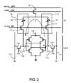
- FIG. 2is a schematic diagram of the non-volatile static random access memory of the present invention in data storage cycle
- FIG. 3is a schematic diagram of the non-volatile static random access memory of the present invention in data recall cycle.
- the present inventionis directed to memory, more particularly, to a static random access memory (SRAM) cell coupled to a non-volatile random access memory (nvRAM) cell.
- SRAMstatic random access memory
- nvRAMnon-volatile random access memory
- the resulting non-volatile static random access memory (nvSRAM)utilizes the nvRAM cell for data storage and recall upon power failure in the SRAM cell.
- the present disclosurerelates to a non-volatile static random access memory (nvSRAM) that utilizes non-volatile data retention as well as fast SRAM operation.
- nvSRAMhas two different modes of operation: SRAM mode and non-volatile mode.
- SRAM modeSRAM mode
- non-volatile modeSRAM mode
- the nvSRAMtakes advantages of fast data read/write operations and it is a solution where reliable data retention has to be guaranteed under extreme conditions.
- the nvSRAMalso reduces the number of integrated circuits and increases the flexibility and power of the system.
- the nvSRAM cell of this inventionutilizes variable magnetic resistors as a non-volatile memory device connected with six transistor static random access memory (6T SRAM) cell. It also includes three transistors to operate the nvSRAM function. One transistor is coupled with each variable magnetic resistor to provide a stack. The two stacks are connected in parallel between the 6T SRAM and the third transistor.
- 6T SRAMsix transistor static random access memory
- the operation of the nvSRAM cell for data storage and recallis implemented by the variable magnetic switching resistors. Since the non-volatile memory portion is employed with magnetic resistive switching or spin-torque magnetic resistor devices, the nvSRAM cell has the more flexible chip integrity of non-volatile memories over SRAMs.
- the nvSRAM cell of this inventionalso provides small operating voltages of non-volatile memory and fast data processing such as SRAM read/write operation and data store/recall. Further, the design does not require the previously required data reset step prior to storing new data in the nvSRAM, since the resistance of the variable magnetic switching resistors will vary based on current direction, which is controlled by the SRAM.
- FIG. 1Ais illustrated a schematic diagram or a circuit diagram of the non-volatile static random access memory (nvSRAM) cell of this invention.
- nvSRAM cell 1has a volatile portion 100 A and a non-volatile portion 10 .
- Volatile portion 100 Ais a SRAM cell, particularly, a six transistor SRAM cell, commonly referred to as a 6T SRAM cell. 6T SRAM cell 100 A of FIG. 1A is briefly discussed below.
- the non-volatile portion, nvRAM 10has a first stack 12 and a second stack 13 .
- First stack 12has a first transistor 21 and a first variable magnetic resistor 23 .
- second stack 13has a second transistor 31 and a second variable magnetic resistor 33 .
- nvRAM 10also has a third transistor 41 .
- the resistances across transistor 21 and transistor 31are approximately equal.
- Stacks 12 , 13are electrically and operationally connected in parallel to third transistor 41 . At their other end, stacks 12 , 13 are electrically and operationally connected to 6T SRAM 100 A.
- Stacks 12 , 13are oriented so that variable magnetic resistors 23 , 33 are electrically positioned between third transistor 41 and transistors 21 , 31 .
- Variable magnetic resistors 23 , 33may alternately be referred to as spin-torque magnetic resistors or magnetic tunnel junctions.
- One type of conventional variable magnetic resistoris a spin valve, which includes an antiferromagnetic layer, a ferromagnetic pinned layer, a ferromagnetic free layer, and a nonmagnetic yet conductive spacer layer between the pinned layer and the free layer.
- the antiferromagnetic layeris used to fix, or pin, the magnetization orientation of the pinned layer in a particular direction.
- the magnetization orientation of the free layeris free to rotate, typically in response to an external field.
- Another conventional variable magnetic resistoris a magnetic tunneling junction or spin tunneling junction. Portions of the spin tunneling junction are analogous to the spin valve.
- the tunnel junctionhas an antiferromagnetic layer, a pinned layer, an insulating barrier layer and a free layer.
- the barrier layeris sufficiently thin to allow electrons to tunnel therethrough.
- the resistance of the elementchanges depending upon the orientations of the magnetizations of the free layer and the pinned layer.
- the resistance of the magnetic elementis low, R L .
- the resistance differential in the variable magnetic resistorsis large (i.e., R H >>R L ).
- the magnetization orientationsare antiparallel
- the magnetization orientationsare parallel.
- nvRAM 10has three voltage sources.
- a first voltage sourceidentified as VGSW in FIG. 1A , is electrically connected to first and second transistors 21 , 31 to enable transistors 21 , 31 .
- a second voltage sourceidentified as VENB in FIG. 1A , is electrically connected to third transistor 41 to enable transistor 41 .
- a third voltage sourceidentified as VDSW, is connected to third transistor 41 at its source/drain terminal, opposite the connection to stacks 12 , 13 .
- Stacks 12 , 13are connected to SRAM cell 100 A.
- SRAM cell 100 Ais a six transistor SRAM cell, commonly referred to as a 6T SRAM cell.
- 6T SRAM cell 100 Ahas six transistors, 101 , 102 , 103 , 104 , 105 and 106 .
- Transistors 101 , 102are commonly referred to as access transistors, and have equal resistance values.
- Transistors 103 , 104are n-type transistors and transistors 105 , 106 are p-type transistors.
- SRAM cell 100 Ais electrically connected to a word line WL 110 to enable transistors 101 , 102 , first and second bit lines BL 111 and BL′ 112 , a voltage ground 115 , and a voltage drain or source 116 .
- a first bit of datacan be stored at node Q 123 and a second bit of data can be stored at node Q 124 .
- Access to 6T SRAM cell 100 Ais enabled by word line WL 110 , which controls access transistors 101 , 102 , which in turn controls whether cell 100 A is electrically connected to bit line BL 111 and BL′ 112 , respectively.
- Access transistor 101has a first source/drain terminal connected to storage node Q 123 that is formed by the junction of n-type resistor 103 and p-type resistor 105 , and a second source/drain terminal connected to the bit line BL 111 .
- Access transistor 102has a first source/drain terminal connected to storage node Q 124 that is formed by the junction of n-type resistor 104 and p-type resistor 106 , and a second source/drain terminal connected to the bit line BL′ 112 . Access transistors 101 , 102 transfer data for both read and write operations.
- SRAM cell 100 Bis a six transistor SRAM cell and can be one conventionally known.
- SRAM cell 100 Bhas a first inverter 121 and a second inverter 122 coupled such that the output of first inverter 121 is connected to the input of second inverter 122 and the output of second inverter 122 is connected to the input of first inverter 121 , to form a bistable latch.
- First and second inverters 121 , 122each consist of an n-type metal oxide semiconductor (MOS) transistor and a p-type MOS transistor configured as the well known complementary metal oxide semiconductor (CMOS) inverter.
- MOSmetal oxide semiconductor
- CMOScomplementary metal oxide semiconductor
- a first access transistor 101 Ahas a first source/drain terminal connected to a storage node Q 123 A that is formed by the junction of the input of first inverter 121 and the output of second inverter 122 and a second source/drain terminal connected to the bit line BL 111 A.
- a second access transistor 102 Ahas a first source/drain terminal connected to the complementary storage node Q 124 A that is formed by the input of second inverter 122 and the output of first inverter 121 and a second source/drain terminal connected to the bit line BL′ 112 A.
- the gates of the first and second access transistors 101 A, 102 Aare connected to word line WL 110 A to receive the activation signals for enabling SRAM cell 100 B.
- the gates of the n-type MOS transistor and the p-type MOS transistor of first inverter 121are connected to a common drain connection of the n-type MOS transistor and the p-type MOS transistor of second inverter 122 , and the gates of the n-type MOS transistor and the p-type MOS transistor of second inverter 122 are connected to the common drain connection of the n-type MOS transistor and the p-type MOS transistor of first inverter 121 .
- nvRAM 10Electrically connected to either SRAM 100 A or SRAM 100 B, between access transistors 101 , 101 A and 102 , 102 A and storage node Q 123 , 123 A and storage node Q 124 , 124 A, respectively, is nvRAM 10 according to the present invention.
- nvRAM 10has two parallel stacks, each having a transistor and a variable magnetic resistor, connected to a third transistor.
- nvRAM cell 10provides data storage and recall upon power failure in SRAM 101 A, 100 B.
- the operation of the nvSRAM cell of this inventiondepends on the variable magnetic switching resistors, or spin-torque magnetic resistor devices, as their resistance varies based on current direction, which is controlled by the output from the CMOS latch of the SRAM.
- nvRAM 10having the three transistors and two variable magnetic resistors provides non-volatile memory that is improved over conventional EEPROM non-volatile memories, at least because it occupies less chip area, is more flexible in its configuration, is less expensive to manufacture, and has a much faster operational speed (e.g., about 1 ns) compared to EEPROM non-volatile memory with transistors (e.g., about 10 ns). Additionally, non-volatile memory of this invention, nvRAM 10 , operates at low power and at low voltage, similar to the voltage of SRAM 100 A or SRAM 100 B, as compared to an EEPROM non-volatile memory that operates at high voltage.
- FIG. 2illustrates a general sequence for storing data from SRAM 100 A to nvRAM 10 .
- third transistor 41is disabled, by having voltage sources VENB and VDSW both off, and transistors 21 , 31 in stacks 12 , 13 are enabled by having voltage sources VGSW on.
- word line WL 110 and bit lines BL 111 , BL′ 112are off and voltage drain/source 116 is on. This creates a closed loop from SRAM 100 A through nvRAM 10 and stacks 12 , 13 .
- variable resistor 23 of first stack 12is designed to have the magnetization orientations in antiparallel configuration due to the illustrated current direction, and thus have a high resistance value R H .
- Variable resistor 33 of second stack 13is designed to have the magnetization orientations in parallel configuration due to the illustrated current direction, and to switch to a low resistance value R L .
- variable resistor 23 of first stack 12will switch to a low resistance value R L and variable resistor 33 of second stack 13 will switch to a high resistance value R H .
- nvRAM 10is designed so that the resistance differential in the variable magnetic resistors is large (i.e., R H >>R L ) and that R H is greater than the resistance of any of the transistors (R N ; i.e., transistors 21 , 31 , 101 , etc.) so that nvRAM 10 can restore data in SRAM cell 100 A from resistors 23 , 33 without loosing the previous states contained in SRAM cell 100 A before the power is turned off.
- FIG. 3illustrates a general sequence for retrieving or recalling data from nvRAM 10 to SRAM 100 A.
- third transistor 41is enabled, by having voltage sources VENB and VDSW both on, and transistors 21 , 31 in stacks 12 , 13 are enabled by having voltage source VGSW on.
- word line WL 110is on, and bit lines BL 111 , BL′ 112 and voltage drain/source 116 are grounded.
- the resulting flow of currentis from voltage source VDSW, through transistor 41 , then parallel through stack 12 to node Q 123 and access transistor 101 to bit line BL 111 and through stack 13 to node Q 124 and access transistor 102 to bit line BL′ 112 .
- the voltage at node Q 123 and node Q 124will be directly related to the resistance of variable magnetic resistors 23 , 33 (i.e., R H or R L ), and will provide the data bit to bit line BL 111 and bit line BL′ 112 , respectively.
- V 41is the voltage at third transistor 41
- R 21 and R 31are the resistance across the transistors 21 , 31 , respectively
- R 101 and R 102are the resistance across access transistors 101 , 102 , respectively.
Landscapes
- Engineering & Computer Science (AREA)
- Microelectronics & Electronic Packaging (AREA)
- Computer Hardware Design (AREA)
- Static Random-Access Memory (AREA)
- Mram Or Spin Memory Techniques (AREA)
Abstract
Description
V123=V41*R101/(RH+R21+R101)
and the voltage at
V124=V41*R102/(RL+R31+R102)
Claims (7)
Priority Applications (1)
| Application Number | Priority Date | Filing Date | Title |
|---|---|---|---|
| US12/370,164US8194438B2 (en) | 2009-02-12 | 2009-02-12 | nvSRAM having variable magnetic resistors |
Applications Claiming Priority (1)
| Application Number | Priority Date | Filing Date | Title |
|---|---|---|---|
| US12/370,164US8194438B2 (en) | 2009-02-12 | 2009-02-12 | nvSRAM having variable magnetic resistors |
Publications (2)
| Publication Number | Publication Date |
|---|---|
| US20100202191A1 US20100202191A1 (en) | 2010-08-12 |
| US8194438B2true US8194438B2 (en) | 2012-06-05 |
Family
ID=42540283
Family Applications (1)
| Application Number | Title | Priority Date | Filing Date |
|---|---|---|---|
| US12/370,164Expired - Fee RelatedUS8194438B2 (en) | 2009-02-12 | 2009-02-12 | nvSRAM having variable magnetic resistors |
Country Status (1)
| Country | Link |
|---|---|
| US (1) | US8194438B2 (en) |
Cited By (20)
| Publication number | Priority date | Publication date | Assignee | Title |
|---|---|---|---|---|
| US20120280713A1 (en)* | 2011-01-20 | 2012-11-08 | Yoshikazu Katoh | Nonvolatile latch circuit and nonvolatile flip-flop circuit |
| US20120320658A1 (en)* | 2011-06-15 | 2012-12-20 | Industrial Technology Research Institute | Nonvolatile static random access memory cell and memory circuit |
| US20130039119A1 (en)* | 2010-03-22 | 2013-02-14 | Qualcomm Incorporated | Memory cell that includes multiple non-volatile memories |
| US20130107606A1 (en)* | 2011-02-07 | 2013-05-02 | Yoshikazu Katoh | Nonvolatile latch circuit, nonvolatile flip-flop circuit, and nonvolatile signal processing device |
| US20130286721A1 (en)* | 2012-04-25 | 2013-10-31 | Industry Academic Cooperation, Yonsei University | Low sensing current non-volatile flip-flop |
| US9349440B1 (en) | 2014-12-11 | 2016-05-24 | Empire Technology Development Llc | Non-volatile SRAM with multiple storage states |
| US9378807B2 (en) | 2014-07-30 | 2016-06-28 | Winbond Electronics Corp. | Non-volatile static random access memory circuits |
| US9401207B2 (en)* | 2014-12-12 | 2016-07-26 | Freescale Semiconductor, Inc. | Pseudo SRAM using resistive elements for non-volatile storage |
| US9401198B1 (en) | 2015-06-30 | 2016-07-26 | Freescale Semiconductor, Inc. | Non-volatile dynamic random access memory (NVDRAM) |
| TWI556235B (en)* | 2013-08-16 | 2016-11-01 | 英特爾股份有限公司 | Memory cell with retention using resistive memory |
| US9548117B2 (en) | 2013-12-06 | 2017-01-17 | Empire Technology Development Llc | Non-volatile SRAM with multiple storage states |
| US9646694B2 (en) | 2014-10-21 | 2017-05-09 | Cypress Semiconductor Corporation | 10-transistor non-volatile static random-access memory using a single non-volatile memory element and method of operation thereof |
| WO2017091709A1 (en) | 2015-11-25 | 2017-06-01 | Akamai Technologies, Inc. | Uniquely identifying and securely communicating with an appliance in an uncontrolled network |
| US20180174644A1 (en)* | 2016-12-21 | 2018-06-21 | Imec Vzw | Non-volatile sram cell using resistive memory elements |
| US10063653B2 (en) | 2014-12-29 | 2018-08-28 | Akamai Technologies, Inc. | Distributed server architecture for supporting a predictive content pre-fetching service for mobile device users |
| US20190066807A1 (en)* | 2017-08-31 | 2019-02-28 | Micron Technology, Inc. | Responding to power loss |
| US20190244666A1 (en)* | 2018-02-04 | 2019-08-08 | Fu-Chang Hsu | Methods and apparatus for memory cells that combine static ram and non volatile memory |
| US10388388B2 (en) | 2017-08-31 | 2019-08-20 | Micron Technology, Inc. | Responding to power loss |
| US10771583B2 (en) | 2014-12-29 | 2020-09-08 | Akamai Technologies, Inc. | Managing mobile device user subscription and service preferences to predictively pre-fetch content |
| US10785293B2 (en) | 2014-11-11 | 2020-09-22 | Akamai Technologies, Inc. | Content delivery to physically-proximate devices using a mesh-assisted cache |
Families Citing this family (20)
| Publication number | Priority date | Publication date | Assignee | Title |
|---|---|---|---|---|
| US20080229269A1 (en)* | 2007-03-12 | 2008-09-18 | International Business Machines Corporation | Design structure for integrating nonvolatile memory capability within sram devices |
| US7692954B2 (en)* | 2007-03-12 | 2010-04-06 | International Business Machines Corporation | Apparatus and method for integrating nonvolatile memory capability within SRAM devices |
| FR2970593B1 (en) | 2011-01-19 | 2013-08-02 | Centre Nat Rech Scient | COMPATIBLE VOLATILE / NON-VOLATILE MEMORY CELL |
| FR2970589B1 (en) | 2011-01-19 | 2013-02-15 | Centre Nat Rech Scient | VOLATILE MEMORY CELL / NON VOLATILE |
| FR2970592B1 (en) | 2011-01-19 | 2013-02-15 | Centre Nat Rech Scient | PROGRAMMABLE VOLATILE / NON-VOLATILE MEMORY CELL |
| FR2976712B1 (en)* | 2011-06-15 | 2014-01-31 | Centre Nat Rech Scient | NON-VOLATILE MEMORY ELEMENT |
| FR2976711B1 (en) | 2011-06-15 | 2014-01-31 | Centre Nat Rech Scient | MEMORY CELL WITH VOLATILE AND NON-VOLATILE MEMORIZATION |
| US8817516B2 (en)* | 2012-02-17 | 2014-08-26 | Semiconductor Energy Laboratory Co., Ltd. | Memory circuit and semiconductor device |
| FR2990089B1 (en)* | 2012-04-27 | 2014-04-11 | Commissariat Energie Atomique | REPROGRAMMABLE LOGIC DEVICE RESISTANT TO RADIATION. |
| EP3107105B1 (en)* | 2012-05-18 | 2021-06-16 | Japan Science and Technology Agency | Memory circuit |
| JP6213092B2 (en)* | 2012-12-17 | 2017-10-18 | 凸版印刷株式会社 | Nonvolatile flip-flop, nonvolatile latch, and nonvolatile memory element |
| FR3004576B1 (en) | 2013-04-15 | 2019-11-29 | Commissariat A L'energie Atomique Et Aux Energies Alternatives | MEMORY CELL WITH NON-VOLATILE DATA STORAGE |
| FR3004577A1 (en) | 2013-04-15 | 2014-10-17 | Commissariat Energie Atomique | |
| FR3008219B1 (en) | 2013-07-05 | 2016-12-09 | Commissariat Energie Atomique | NON-VOLATILE MEMORY DEVICE |
| TWI678768B (en)* | 2014-11-20 | 2019-12-01 | 日商新力股份有限公司 | Semiconductor device |
| US10319425B1 (en)* | 2018-03-29 | 2019-06-11 | QUALCOMM Technologies Incorporated | Offset-cancellation sensing circuit (OCSC)-based non-volatile (NV) memory circuits |
| CN113342253B (en)* | 2020-03-03 | 2025-03-11 | 北京时代全芯存储技术股份有限公司 | Hybrid Memory |
| CN113360076B (en)* | 2020-03-03 | 2025-03-11 | 北京时代全芯存储技术股份有限公司 | Hybrid Memory Cell |
| US11145348B1 (en)* | 2020-05-11 | 2021-10-12 | Globalfoundries U.S. Inc. | Circuit structure and method for memory storage with memory cell and MRAM stack |
| JP7351576B1 (en)* | 2023-02-14 | 2023-09-27 | 秀治 小池 | Bidirectional data transmission circuit |
Citations (17)
| Publication number | Priority date | Publication date | Assignee | Title |
|---|---|---|---|---|
| US5488579A (en) | 1994-04-29 | 1996-01-30 | Motorola Inc. | Three-dimensionally integrated nonvolatile SRAM cell and process |
| US5680363A (en) | 1992-09-17 | 1997-10-21 | Mitsubishi Denki Kabushiki Kaisha | Semiconductor memory capable of transferring data at a high speed between an SRAM and a DRAM array |
| US6097629A (en) | 1998-09-30 | 2000-08-01 | Simtek Corporation | Non-volatile, static random access memory with high speed store capability |
| US6414873B1 (en) | 2001-03-16 | 2002-07-02 | Simtek Corporation | nvSRAM with multiple non-volatile memory cells for each SRAM memory cell |
| US6714444B2 (en)* | 2002-08-06 | 2004-03-30 | Grandis, Inc. | Magnetic element utilizing spin transfer and an MRAM device using the magnetic element |
| US7082053B1 (en)* | 2003-12-24 | 2006-07-25 | Silicon Magnetic Systems | Non-volatile latch with magnetic junctions |
| US7164608B2 (en) | 2004-07-28 | 2007-01-16 | Aplus Flash Technology, Inc. | NVRAM memory cell architecture that integrates conventional SRAM and flash cells |
| US7173841B2 (en)* | 2004-12-03 | 2007-02-06 | Taiwan Semiconductor Manufacturing Company, Ltd. | Magnetic memory array |
| US7206217B2 (en)* | 2002-04-10 | 2007-04-17 | Matsushita Electric Industrial Co., Ltd. | Non-volatile flip flop |
| US7280397B2 (en) | 2005-07-11 | 2007-10-09 | Sandisk 3D Llc | Three-dimensional non-volatile SRAM incorporating thin-film device layer |
| US7379327B2 (en)* | 2006-06-26 | 2008-05-27 | Grandis, Inc. | Current driven switching of magnetic storage cells utilizing spin transfer and magnetic memories using such cells having enhanced read and write margins |
| US20080151624A1 (en) | 2006-12-22 | 2008-06-26 | Still David W | Combination SRAM and NVSRAM semiconductor memory array |
| US7599210B2 (en)* | 2005-08-19 | 2009-10-06 | Sony Corporation | Nonvolatile memory cell, storage device and nonvolatile logic circuit |
| US7692954B2 (en)* | 2007-03-12 | 2010-04-06 | International Business Machines Corporation | Apparatus and method for integrating nonvolatile memory capability within SRAM devices |
| US7791941B2 (en)* | 2007-10-26 | 2010-09-07 | Micron Technology, Inc. | Non-volatile SRAM cell |
| US7903451B2 (en)* | 2008-09-25 | 2011-03-08 | Kabushiki Kaisha Toshiba | Storage apparatus including non-volatile SRAM |
| US20120020159A1 (en)* | 2009-08-19 | 2012-01-26 | Grandis, Inc. | Non-volatile static ram cell circuit and timing method |
- 2009
- 2009-02-12USUS12/370,164patent/US8194438B2/ennot_activeExpired - Fee Related
Patent Citations (17)
| Publication number | Priority date | Publication date | Assignee | Title |
|---|---|---|---|---|
| US5680363A (en) | 1992-09-17 | 1997-10-21 | Mitsubishi Denki Kabushiki Kaisha | Semiconductor memory capable of transferring data at a high speed between an SRAM and a DRAM array |
| US5488579A (en) | 1994-04-29 | 1996-01-30 | Motorola Inc. | Three-dimensionally integrated nonvolatile SRAM cell and process |
| US6097629A (en) | 1998-09-30 | 2000-08-01 | Simtek Corporation | Non-volatile, static random access memory with high speed store capability |
| US6414873B1 (en) | 2001-03-16 | 2002-07-02 | Simtek Corporation | nvSRAM with multiple non-volatile memory cells for each SRAM memory cell |
| US7206217B2 (en)* | 2002-04-10 | 2007-04-17 | Matsushita Electric Industrial Co., Ltd. | Non-volatile flip flop |
| US6714444B2 (en)* | 2002-08-06 | 2004-03-30 | Grandis, Inc. | Magnetic element utilizing spin transfer and an MRAM device using the magnetic element |
| US7082053B1 (en)* | 2003-12-24 | 2006-07-25 | Silicon Magnetic Systems | Non-volatile latch with magnetic junctions |
| US7164608B2 (en) | 2004-07-28 | 2007-01-16 | Aplus Flash Technology, Inc. | NVRAM memory cell architecture that integrates conventional SRAM and flash cells |
| US7173841B2 (en)* | 2004-12-03 | 2007-02-06 | Taiwan Semiconductor Manufacturing Company, Ltd. | Magnetic memory array |
| US7280397B2 (en) | 2005-07-11 | 2007-10-09 | Sandisk 3D Llc | Three-dimensional non-volatile SRAM incorporating thin-film device layer |
| US7599210B2 (en)* | 2005-08-19 | 2009-10-06 | Sony Corporation | Nonvolatile memory cell, storage device and nonvolatile logic circuit |
| US7379327B2 (en)* | 2006-06-26 | 2008-05-27 | Grandis, Inc. | Current driven switching of magnetic storage cells utilizing spin transfer and magnetic memories using such cells having enhanced read and write margins |
| US20080151624A1 (en) | 2006-12-22 | 2008-06-26 | Still David W | Combination SRAM and NVSRAM semiconductor memory array |
| US7692954B2 (en)* | 2007-03-12 | 2010-04-06 | International Business Machines Corporation | Apparatus and method for integrating nonvolatile memory capability within SRAM devices |
| US7791941B2 (en)* | 2007-10-26 | 2010-09-07 | Micron Technology, Inc. | Non-volatile SRAM cell |
| US7903451B2 (en)* | 2008-09-25 | 2011-03-08 | Kabushiki Kaisha Toshiba | Storage apparatus including non-volatile SRAM |
| US20120020159A1 (en)* | 2009-08-19 | 2012-01-26 | Grandis, Inc. | Non-volatile static ram cell circuit and timing method |
Non-Patent Citations (1)
| Title |
|---|
| Zhao et al., "Integration of Spin-RAM technology in FPGA Circuits" Solid-State and Integrated Circuit Technology, 2006. ICSICT '06. 8th International Conference on, Originally published: Oct. 23-26, 2006, Version Presented Apr. 23, 2007, pp. 799-802, Digital Object Identifier: 10.1109/ICSICT.2006.306511.* |
Cited By (33)
| Publication number | Priority date | Publication date | Assignee | Title |
|---|---|---|---|---|
| US8867258B2 (en)* | 2010-03-22 | 2014-10-21 | Qualcomm Incorporated | Memory cell that includes multiple non-volatile memories |
| US20130039119A1 (en)* | 2010-03-22 | 2013-02-14 | Qualcomm Incorporated | Memory cell that includes multiple non-volatile memories |
| US8437177B2 (en)* | 2011-01-20 | 2013-05-07 | Panasonic Corporation | Nonvolatile latch circuit and nonvolatile flip-flop circuit |
| US20120280713A1 (en)* | 2011-01-20 | 2012-11-08 | Yoshikazu Katoh | Nonvolatile latch circuit and nonvolatile flip-flop circuit |
| US20130107606A1 (en)* | 2011-02-07 | 2013-05-02 | Yoshikazu Katoh | Nonvolatile latch circuit, nonvolatile flip-flop circuit, and nonvolatile signal processing device |
| US8619466B2 (en)* | 2011-02-07 | 2013-12-31 | Panasonic Corporation | Nonvolatile latch circuit, nonvolatile flip-flop circuit, and nonvolatile signal processing device |
| US20120320658A1 (en)* | 2011-06-15 | 2012-12-20 | Industrial Technology Research Institute | Nonvolatile static random access memory cell and memory circuit |
| US8508983B2 (en)* | 2011-06-15 | 2013-08-13 | Industrial Technology Research Institute | Nonvolatile static random access memory cell and memory circuit |
| US20130286721A1 (en)* | 2012-04-25 | 2013-10-31 | Industry Academic Cooperation, Yonsei University | Low sensing current non-volatile flip-flop |
| US9196337B2 (en)* | 2012-04-25 | 2015-11-24 | Qualcomm Incorporated | Low sensing current non-volatile flip-flop |
| TWI556235B (en)* | 2013-08-16 | 2016-11-01 | 英特爾股份有限公司 | Memory cell with retention using resistive memory |
| US9966140B2 (en) | 2013-12-06 | 2018-05-08 | Empire Technology Development Llc | Non-volatile SRAM with multiple storage states |
| US9548117B2 (en) | 2013-12-06 | 2017-01-17 | Empire Technology Development Llc | Non-volatile SRAM with multiple storage states |
| US9378807B2 (en) | 2014-07-30 | 2016-06-28 | Winbond Electronics Corp. | Non-volatile static random access memory circuits |
| US9646694B2 (en) | 2014-10-21 | 2017-05-09 | Cypress Semiconductor Corporation | 10-transistor non-volatile static random-access memory using a single non-volatile memory element and method of operation thereof |
| US9997237B2 (en) | 2014-10-21 | 2018-06-12 | Cypress Semiconductor Corporation | 10-transistor non-volatile static random-access memory using a single non-volatile memory element and method of operation thereof |
| US10785293B2 (en) | 2014-11-11 | 2020-09-22 | Akamai Technologies, Inc. | Content delivery to physically-proximate devices using a mesh-assisted cache |
| US9349440B1 (en) | 2014-12-11 | 2016-05-24 | Empire Technology Development Llc | Non-volatile SRAM with multiple storage states |
| US9401207B2 (en)* | 2014-12-12 | 2016-07-26 | Freescale Semiconductor, Inc. | Pseudo SRAM using resistive elements for non-volatile storage |
| US10063653B2 (en) | 2014-12-29 | 2018-08-28 | Akamai Technologies, Inc. | Distributed server architecture for supporting a predictive content pre-fetching service for mobile device users |
| US10771583B2 (en) | 2014-12-29 | 2020-09-08 | Akamai Technologies, Inc. | Managing mobile device user subscription and service preferences to predictively pre-fetch content |
| US9401198B1 (en) | 2015-06-30 | 2016-07-26 | Freescale Semiconductor, Inc. | Non-volatile dynamic random access memory (NVDRAM) |
| WO2017091709A1 (en) | 2015-11-25 | 2017-06-01 | Akamai Technologies, Inc. | Uniquely identifying and securely communicating with an appliance in an uncontrolled network |
| US10325647B2 (en)* | 2016-12-21 | 2019-06-18 | Imec Vzw | Non-volatile SRAM cell using resistive memory elements |
| US20180174644A1 (en)* | 2016-12-21 | 2018-06-21 | Imec Vzw | Non-volatile sram cell using resistive memory elements |
| US10373694B2 (en)* | 2017-08-31 | 2019-08-06 | Micron Technology, Inc. | Responding to power loss |
| US10388388B2 (en) | 2017-08-31 | 2019-08-20 | Micron Technology, Inc. | Responding to power loss |
| US10762971B2 (en) | 2017-08-31 | 2020-09-01 | Micron Technology, Inc. | Responding to power loss |
| US20190066807A1 (en)* | 2017-08-31 | 2019-02-28 | Micron Technology, Inc. | Responding to power loss |
| US10803964B2 (en) | 2017-08-31 | 2020-10-13 | Micron Technology, Inc. | Responding to power loss |
| US11017868B2 (en) | 2017-08-31 | 2021-05-25 | Micron Technology, Inc. | Responding to power loss |
| US11322211B2 (en) | 2017-08-31 | 2022-05-03 | Micron Technology, Inc. | Memory devices having a differential storage device |
| US20190244666A1 (en)* | 2018-02-04 | 2019-08-08 | Fu-Chang Hsu | Methods and apparatus for memory cells that combine static ram and non volatile memory |
Also Published As
| Publication number | Publication date |
|---|---|
| US20100202191A1 (en) | 2010-08-12 |
Similar Documents
| Publication | Publication Date | Title |
|---|---|---|
| US8194438B2 (en) | nvSRAM having variable magnetic resistors | |
| US9230627B2 (en) | High density low power GSHE-STT MRAM | |
| US10748592B2 (en) | Compact magnetic storage memory cell | |
| EP2130206B1 (en) | Read disturb reduction circuit for spin transfer torque magnetoresistive random access memory | |
| US6865106B2 (en) | Bridge-type magnetic random access memory (MRAM) latch | |
| US6343032B1 (en) | Non-volatile spin dependent tunnel junction circuit | |
| US7173846B2 (en) | Magnetic RAM and array architecture using a two transistor, one MTJ cell | |
| US8077501B2 (en) | Differential read and write architecture | |
| US20040052106A1 (en) | Semiconductor memory device with latch circuit and two magneto-resistance elements | |
| TW200425161A (en) | Temperature compensated RRAM circuit | |
| EP3109863B1 (en) | Memory circuit | |
| US6930910B2 (en) | Magnetic random access memory cell device using magnetic tunnel junction | |
| US12254923B2 (en) | Nonvolatile SRAM | |
| US7511992B2 (en) | Magnetic memory device | |
| US8203869B2 (en) | Bit line charge accumulation sensing for resistive changing memory | |
| WO2007067832A2 (en) | Mram with a write driver and method therefor | |
| CN100361230C (en) | Thin film magnetic memory device with memory cell having magnetic tunnel junction | |
| US8107285B2 (en) | Read direction for spin-torque based memory device | |
| US7372723B1 (en) | State save-on-power-down using GMR non-volatile elements | |
| US7092285B1 (en) | State save-on-power-down using GMR non-volatile elements | |
| KR100782944B1 (en) | Low power magnetic memory device |
Legal Events
| Date | Code | Title | Description |
|---|---|---|---|
| AS | Assignment | Owner name:SEAGATE TECHNOLOGY LLC, CALIFORNIA Free format text:ASSIGNMENT OF ASSIGNORS INTEREST;ASSIGNORS:AHN, YONGCHUL;KHOUEIR, ANTOINE;LU, YONG;AND OTHERS;REEL/FRAME:022251/0353 Effective date:20090212 | |
| AS | Assignment | Owner name:WELLS FARGO BANK, NATIONAL ASSOCIATION, AS COLLATERAL AGENT AND SECOND PRIORITY REPRESENTATIVE, CALIFORNIA Free format text:SECURITY AGREEMENT;ASSIGNORS:MAXTOR CORPORATION;SEAGATE TECHNOLOGY LLC;SEAGATE TECHNOLOGY INTERNATIONAL;REEL/FRAME:022757/0017 Effective date:20090507 Owner name:JPMORGAN CHASE BANK, N.A., AS ADMINISTRATIVE AGENT AND FIRST PRIORITY REPRESENTATIVE, NEW YORK Free format text:SECURITY AGREEMENT;ASSIGNORS:MAXTOR CORPORATION;SEAGATE TECHNOLOGY LLC;SEAGATE TECHNOLOGY INTERNATIONAL;REEL/FRAME:022757/0017 Effective date:20090507 Owner name:WELLS FARGO BANK, NATIONAL ASSOCIATION, AS COLLATE Free format text:SECURITY AGREEMENT;ASSIGNORS:MAXTOR CORPORATION;SEAGATE TECHNOLOGY LLC;SEAGATE TECHNOLOGY INTERNATIONAL;REEL/FRAME:022757/0017 Effective date:20090507 Owner name:JPMORGAN CHASE BANK, N.A., AS ADMINISTRATIVE AGENT Free format text:SECURITY AGREEMENT;ASSIGNORS:MAXTOR CORPORATION;SEAGATE TECHNOLOGY LLC;SEAGATE TECHNOLOGY INTERNATIONAL;REEL/FRAME:022757/0017 Effective date:20090507 | |
| AS | Assignment | Owner name:SEAGATE TECHNOLOGY LLC, CALIFORNIA Free format text:RELEASE;ASSIGNOR:JPMORGAN CHASE BANK, N.A., AS ADMINISTRATIVE AGENT;REEL/FRAME:025662/0001 Effective date:20110114 Owner name:MAXTOR CORPORATION, CALIFORNIA Free format text:RELEASE;ASSIGNOR:JPMORGAN CHASE BANK, N.A., AS ADMINISTRATIVE AGENT;REEL/FRAME:025662/0001 Effective date:20110114 Owner name:SEAGATE TECHNOLOGY HDD HOLDINGS, CALIFORNIA Free format text:RELEASE;ASSIGNOR:JPMORGAN CHASE BANK, N.A., AS ADMINISTRATIVE AGENT;REEL/FRAME:025662/0001 Effective date:20110114 Owner name:SEAGATE TECHNOLOGY INTERNATIONAL, CALIFORNIA Free format text:RELEASE;ASSIGNOR:JPMORGAN CHASE BANK, N.A., AS ADMINISTRATIVE AGENT;REEL/FRAME:025662/0001 Effective date:20110114 | |
| AS | Assignment | Owner name:THE BANK OF NOVA SCOTIA, AS ADMINISTRATIVE AGENT, CANADA Free format text:SECURITY AGREEMENT;ASSIGNOR:SEAGATE TECHNOLOGY LLC;REEL/FRAME:026010/0350 Effective date:20110118 Owner name:THE BANK OF NOVA SCOTIA, AS ADMINISTRATIVE AGENT, Free format text:SECURITY AGREEMENT;ASSIGNOR:SEAGATE TECHNOLOGY LLC;REEL/FRAME:026010/0350 Effective date:20110118 | |
| AS | Assignment | Owner name:SEAGATE TECHNOLOGY LLC, CALIFORNIA Free format text:TERMINATION AND RELEASE OF SECURITY INTEREST IN PATENT RIGHTS;ASSIGNOR:WELLS FARGO BANK, NATIONAL ASSOCIATION, AS COLLATERAL AGENT AND SECOND PRIORITY REPRESENTATIVE;REEL/FRAME:030833/0001 Effective date:20130312 Owner name:SEAGATE TECHNOLOGY US HOLDINGS, INC., CALIFORNIA Free format text:TERMINATION AND RELEASE OF SECURITY INTEREST IN PATENT RIGHTS;ASSIGNOR:WELLS FARGO BANK, NATIONAL ASSOCIATION, AS COLLATERAL AGENT AND SECOND PRIORITY REPRESENTATIVE;REEL/FRAME:030833/0001 Effective date:20130312 Owner name:EVAULT INC. (F/K/A I365 INC.), CALIFORNIA Free format text:TERMINATION AND RELEASE OF SECURITY INTEREST IN PATENT RIGHTS;ASSIGNOR:WELLS FARGO BANK, NATIONAL ASSOCIATION, AS COLLATERAL AGENT AND SECOND PRIORITY REPRESENTATIVE;REEL/FRAME:030833/0001 Effective date:20130312 Owner name:SEAGATE TECHNOLOGY INTERNATIONAL, CAYMAN ISLANDS Free format text:TERMINATION AND RELEASE OF SECURITY INTEREST IN PATENT RIGHTS;ASSIGNOR:WELLS FARGO BANK, NATIONAL ASSOCIATION, AS COLLATERAL AGENT AND SECOND PRIORITY REPRESENTATIVE;REEL/FRAME:030833/0001 Effective date:20130312 | |
| REMI | Maintenance fee reminder mailed | ||
| LAPS | Lapse for failure to pay maintenance fees | ||
| STCH | Information on status: patent discontinuation | Free format text:PATENT EXPIRED DUE TO NONPAYMENT OF MAINTENANCE FEES UNDER 37 CFR 1.362 | |
| FP | Lapsed due to failure to pay maintenance fee | Effective date:20160605 | |
| AS | Assignment | Owner name:SEAGATE TECHNOLOGY PUBLIC LIMITED COMPANY, CALIFORNIA Free format text:RELEASE BY SECURED PARTY;ASSIGNOR:THE BANK OF NOVA SCOTIA;REEL/FRAME:072193/0001 Effective date:20250303 Owner name:SEAGATE TECHNOLOGY, CALIFORNIA Free format text:RELEASE BY SECURED PARTY;ASSIGNOR:THE BANK OF NOVA SCOTIA;REEL/FRAME:072193/0001 Effective date:20250303 Owner name:SEAGATE TECHNOLOGY HDD HOLDINGS, CALIFORNIA Free format text:RELEASE BY SECURED PARTY;ASSIGNOR:THE BANK OF NOVA SCOTIA;REEL/FRAME:072193/0001 Effective date:20250303 Owner name:I365 INC., CALIFORNIA Free format text:RELEASE BY SECURED PARTY;ASSIGNOR:THE BANK OF NOVA SCOTIA;REEL/FRAME:072193/0001 Effective date:20250303 Owner name:SEAGATE TECHNOLOGY LLC, CALIFORNIA Free format text:RELEASE BY SECURED PARTY;ASSIGNOR:THE BANK OF NOVA SCOTIA;REEL/FRAME:072193/0001 Effective date:20250303 Owner name:SEAGATE TECHNOLOGY INTERNATIONAL, CAYMAN ISLANDS Free format text:RELEASE BY SECURED PARTY;ASSIGNOR:THE BANK OF NOVA SCOTIA;REEL/FRAME:072193/0001 Effective date:20250303 Owner name:SEAGATE HDD CAYMAN, CAYMAN ISLANDS Free format text:RELEASE BY SECURED PARTY;ASSIGNOR:THE BANK OF NOVA SCOTIA;REEL/FRAME:072193/0001 Effective date:20250303 Owner name:SEAGATE TECHNOLOGY (US) HOLDINGS, INC., CALIFORNIA Free format text:RELEASE BY SECURED PARTY;ASSIGNOR:THE BANK OF NOVA SCOTIA;REEL/FRAME:072193/0001 Effective date:20250303 |