US8194366B1 - TMR read head structures with differential stripe heights - Google Patents
TMR read head structures with differential stripe heightsDownload PDFInfo
- Publication number
- US8194366B1 US8194366B1US12/579,315US57931509AUS8194366B1US 8194366 B1US8194366 B1US 8194366B1US 57931509 AUS57931509 AUS 57931509AUS 8194366 B1US8194366 B1US 8194366B1
- Authority
- US
- United States
- Prior art keywords
- layer
- stripe height
- free layer
- pinned
- read head
- Prior art date
- Legal status (The legal status is an assumption and is not a legal conclusion. Google has not performed a legal analysis and makes no representation as to the accuracy of the status listed.)
- Expired - Fee Related, expires
Links
- 230000005291magnetic effectEffects0.000claimsabstractdescription51
- 238000000034methodMethods0.000claimsabstractdescription50
- 230000005641tunnelingEffects0.000claimsabstractdescription34
- 230000004888barrier functionEffects0.000claimsabstractdescription29
- 230000004907fluxEffects0.000claimsdescription17
- 230000005290antiferromagnetic effectEffects0.000claimsdescription9
- 239000011810insulating materialSubstances0.000claimsdescription7
- TWNQGVIAIRXVLR-UHFFFAOYSA-Noxo(oxoalumanyloxy)alumaneChemical compoundO=[Al]O[Al]=OTWNQGVIAIRXVLR-UHFFFAOYSA-N0.000claims2
- 230000008569processEffects0.000description33
- 230000005415magnetizationEffects0.000description12
- 125000006850spacer groupChemical group0.000description6
- 229920002120photoresistant polymerPolymers0.000description5
- 238000000151depositionMethods0.000description4
- 238000013461designMethods0.000description4
- 238000013459approachMethods0.000description3
- 230000008021depositionEffects0.000description3
- CPLXHLVBOLITMK-UHFFFAOYSA-Nmagnesium oxideInorganic materials[Mg]=OCPLXHLVBOLITMK-UHFFFAOYSA-N0.000description3
- 239000000395magnesium oxideSubstances0.000description3
- AXZKOIWUVFPNLO-UHFFFAOYSA-Nmagnesium;oxygen(2-)Chemical compound[O-2].[Mg+2]AXZKOIWUVFPNLO-UHFFFAOYSA-N0.000description3
- 239000000463materialSubstances0.000description3
- 229910052751metalInorganic materials0.000description3
- 239000002184metalSubstances0.000description3
- 230000009467reductionEffects0.000description3
- 230000035945sensitivityEffects0.000description3
- 230000008901benefitEffects0.000description2
- 230000005540biological transmissionEffects0.000description2
- 230000001427coherent effectEffects0.000description2
- 238000010586diagramMethods0.000description2
- 238000004519manufacturing processMethods0.000description2
- 150000002739metalsChemical class0.000description2
- 238000003801millingMethods0.000description2
- 230000004048modificationEffects0.000description2
- 238000012986modificationMethods0.000description2
- 238000004088simulationMethods0.000description2
- MYMOFIZGZYHOMD-UHFFFAOYSA-NDioxygenChemical compoundO=OMYMOFIZGZYHOMD-UHFFFAOYSA-N0.000description1
- 229910019041PtMnInorganic materials0.000description1
- KJTLSVCANCCWHF-UHFFFAOYSA-NRutheniumChemical compound[Ru]KJTLSVCANCCWHF-UHFFFAOYSA-N0.000description1
- 229910003481amorphous carbonInorganic materials0.000description1
- 239000004020conductorSubstances0.000description1
- 229910052802copperInorganic materials0.000description1
- 230000005347demagnetizationEffects0.000description1
- 238000011161developmentMethods0.000description1
- 239000003989dielectric materialSubstances0.000description1
- 229910001882dioxygenInorganic materials0.000description1
- 238000009837dry grindingMethods0.000description1
- 230000000694effectsEffects0.000description1
- 238000005530etchingMethods0.000description1
- 230000005294ferromagnetic effectEffects0.000description1
- 230000006870functionEffects0.000description1
- 230000010354integrationEffects0.000description1
- 230000003993interactionEffects0.000description1
- 229910052749magnesiumInorganic materials0.000description1
- 239000011777magnesiumSubstances0.000description1
- 239000000696magnetic materialSubstances0.000description1
- 230000003647oxidationEffects0.000description1
- 238000007254oxidation reactionMethods0.000description1
- 230000035699permeabilityEffects0.000description1
- 229910052697platinumInorganic materials0.000description1
- 230000004044responseEffects0.000description1
- 229910052707rutheniumInorganic materials0.000description1
- 238000000926separation methodMethods0.000description1
- 239000011800void materialSubstances0.000description1
Images


Classifications
- G—PHYSICS
- G11—INFORMATION STORAGE
- G11B—INFORMATION STORAGE BASED ON RELATIVE MOVEMENT BETWEEN RECORD CARRIER AND TRANSDUCER
- G11B5/00—Recording by magnetisation or demagnetisation of a record carrier; Reproducing by magnetic means; Record carriers therefor
- G11B5/127—Structure or manufacture of heads, e.g. inductive
- G11B5/33—Structure or manufacture of flux-sensitive heads, i.e. for reproduction only; Combination of such heads with means for recording or erasing only
- G11B5/39—Structure or manufacture of flux-sensitive heads, i.e. for reproduction only; Combination of such heads with means for recording or erasing only using magneto-resistive devices or effects
- G11B5/3903—Structure or manufacture of flux-sensitive heads, i.e. for reproduction only; Combination of such heads with means for recording or erasing only using magneto-resistive devices or effects using magnetic thin film layers or their effects, the films being part of integrated structures
- G11B5/398—Specially shaped layers
- G—PHYSICS
- G01—MEASURING; TESTING
- G01R—MEASURING ELECTRIC VARIABLES; MEASURING MAGNETIC VARIABLES
- G01R33/00—Arrangements or instruments for measuring magnetic variables
- G01R33/02—Measuring direction or magnitude of magnetic fields or magnetic flux
- G01R33/06—Measuring direction or magnitude of magnetic fields or magnetic flux using galvano-magnetic devices
- G01R33/09—Magnetoresistive devices
- G01R33/098—Magnetoresistive devices comprising tunnel junctions, e.g. tunnel magnetoresistance sensors
- G—PHYSICS
- G11—INFORMATION STORAGE
- G11B—INFORMATION STORAGE BASED ON RELATIVE MOVEMENT BETWEEN RECORD CARRIER AND TRANSDUCER
- G11B5/00—Recording by magnetisation or demagnetisation of a record carrier; Reproducing by magnetic means; Record carriers therefor
- G11B5/127—Structure or manufacture of heads, e.g. inductive
- G11B5/33—Structure or manufacture of flux-sensitive heads, i.e. for reproduction only; Combination of such heads with means for recording or erasing only
- G11B5/39—Structure or manufacture of flux-sensitive heads, i.e. for reproduction only; Combination of such heads with means for recording or erasing only using magneto-resistive devices or effects
- G11B5/3903—Structure or manufacture of flux-sensitive heads, i.e. for reproduction only; Combination of such heads with means for recording or erasing only using magneto-resistive devices or effects using magnetic thin film layers or their effects, the films being part of integrated structures
- G11B5/3906—Details related to the use of magnetic thin film layers or to their effects
- G11B5/3909—Arrangements using a magnetic tunnel junction
- H—ELECTRICITY
- H10—SEMICONDUCTOR DEVICES; ELECTRIC SOLID-STATE DEVICES NOT OTHERWISE PROVIDED FOR
- H10N—ELECTRIC SOLID-STATE DEVICES NOT OTHERWISE PROVIDED FOR
- H10N50/00—Galvanomagnetic devices
- H10N50/01—Manufacture or treatment
- H—ELECTRICITY
- H10—SEMICONDUCTOR DEVICES; ELECTRIC SOLID-STATE DEVICES NOT OTHERWISE PROVIDED FOR
- H10N—ELECTRIC SOLID-STATE DEVICES NOT OTHERWISE PROVIDED FOR
- H10N50/00—Galvanomagnetic devices
- H10N50/10—Magnetoresistive devices
Definitions
- the present inventiongenerally relates to magnetic transducers and, in particular, relates to TMR read head structures with differential stripe heights.
- Tunnel magnetoresistance (TMR) read sensorssuch as current-perpendicular-to-plane (CPP) TMR read sensors, are frequently employed as magnetoresistive sensors in the magnetic read heads of hard disk drives.
- Thermal magnetization fluctuationsalso known as magnetic noise
- the magnetic noisescales inversely with the read sensor's volume. It is believed that the magnetic noise poses a fundamental limit to signal-to-noise ratio (SNR) of a magnetic recording system.
- Various embodiments of the subject disclosureaddress the magnetic noise issue associated with reduced TMR read sensor dimensions by providing a novel TMR read sensor structure in which a free layer stripe height is larger than a current path stripe height.
- a differential stripe-height structurecan drastically reduce the magnetic noise while increasing the read sensitivity or utilization factor. Therefore, differential stripe-height TMR read sensor structures of the present disclosure can be suitable for high recording density (e.g., 1000 to 1500 Gbit/in 2 ) application and beyond.
- the subject disclosurealso describes a double lift-off integration process that can be used to produce such a differential stripe-height TMR read sensor structure.
- a tunneling magnetoresistance (TMR) read headcan comprise a free layer having a free layer stripe height, the free layer having a first side and a second side.
- the TMR read headcan further comprise a pinned stack disposed adjacent to the first side of the free layer.
- the pinned stackcan comprise at least one magnetic layer having a current path stripe height that is less than the free layer stripe height.
- a method of producing a tunneling magnetoresistance (TMR) read headcomprising providing a free layer having a free layer stripe height, the free layer having a first side and a second side.
- the methodcan further comprise forming a tunneling barrier layer adjacent to the first side of the free layer, the tunneling barrier layer having a first side and a second side, the second side of the tunneling barrier layer facing the first side of the free layer.
- the methodcan further comprise forming a pinned stack adjacent to the first side of the free layer.
- the pinned stackcan comprise at least one magnetic layer having a current path stripe height that is less than the free layer stripe height.
- FIG. 1is a perspective view of a conventional TMR sensing element which has a uniform stripe height across the track direction.
- FIG. 2is a graph illustrating a linear decay of magnetic flux with the depth of height for a TMR sensing element with a uniform stripe height when the free layer stripe height is comparable to the magnetic transmission line characteristic length.
- FIG. 3is a perspective view of a novel TMR sensing element which has differential stripe heights across a track direction according to one aspect of the subject disclosure.
- FIG. 4is a diagram depicting a TMR read head having a novel TMR sensing element having differential stripe heights according to one aspect of the subject disclosure.
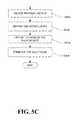
- FIGS. 5A , 5 B and 5 Cprovide a flowchart illustrating an exemplary process for fabricating a TMR read head having differential stripe heights according to one aspect of the subject disclosure.
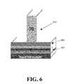
- FIG. 6is an intermediate structure that defines a reader width for a TMR read head having differential stripe heights according to one aspect of the subject disclosure.
- FIG. 1is a perspective view of a conventional TMR sensing element 100 (e.g., a CPP read element) which has a uniform stripe height across a track direction 106 .
- the conventional TMR sensing element 100has a plurality of magnetic layers including a free layer 120 , a pinned stack 102 , and a tunneling barrier layer 130 disposed between the free layer 120 and the pinned stack 102 .
- the free layer 120has a free layer stripe height (D) 105
- the pinned stack 102has a current path stripe height (H) 107 .
- the free layer stripe height (D) 105is same as or comparable to the current path stripe height (H) 107 .
- the uniform read stripe height (e.g., D and H) of the conventional TMR sensing element 100is typically less than or equal to L, a decay length of a magnetic flux ( ⁇ ) 109 emanating from a magnetic recording media (not shown).
- Lcan be expressed (Tg ⁇ /2) 1/2 , where T is the total thickness of the magnetic layers, ⁇ is the permeability of those magnetic layers, and g is a half gap distance 215 as shown in FIG. 2 .
- Tthe total thickness of the magnetic layers
- ⁇the permeability of those magnetic layers
- gis a half gap distance 215 as shown in FIG. 2 .
- FIG. 2shows a TMR sensor structure 210 having a first surface 212 disposed proximate to a magnetic recording medium 220 and a second surface 214 disposed opposite to the first surface 212 at a uniform stripe height (D) from the first surface, wherein a magnetic flux emanating from the magnetic recording medium has a first magnetic flux value at the first surface 212 and a second magnetic flux value at the second surface 214 .
- the magnetic flux ( ⁇ )becomes zero at the second surface 214 (e.g., at the uniform stripe height (D)), analogous to an open-circuited electric transmission line.
- the maximum average flux in the sensor structure 210is always close to 0.5 ⁇ (0) regardless of the actual stripe height D.
- FIG. 3is a perspective view of a novel TMR sensing element 300 (e.g., a CPP read element) which has two or more differential stripe heights across a track direction 306 according to one aspect of the subject disclosure.
- the TMR sensing element 300has a plurality of magnetic layers including a free layer 320 , a pinned stack 302 , and a tunneling (junction) barrier 330 disposed between the free layer 320 and the pinned stack 302 .
- the free layer 320has a free layer stripe height (D) 305
- the pinned stack 302has a current path stripe height (H) 307 .
- the free layer stripe height (D) 305is larger than the current path stripe height (H) 307 .
- D 305is between 20 to 200% larger than H 307 . In some of such embodiments, D 305 is between about 50-100% larger than H 307 .
- the magnetic flux ( ⁇ ) 109can be made nonzero at the end of an electric current path (e.g., at the height of H) in the free layer 305 .
- the maximum average flux through the electric current path of the TMR sensing element 300can be manipulated to be much larger than 0.5 ⁇ (0) owing to the fact that ⁇ (H), the magnetic flux at H, is nonzero.
- the increase in maximum average fluxresults in a number of performance benefits including, but not limited to, achieving a large effective utilization factor, and an improved signal-to-noise ratio (SNR) due to an increase in signal a large free layer volume achieved by having the free layer stripe height (D 305 ) substantially larger than the current stripe height (H 307 ).
- SNRsignal-to-noise ratio
- results of a micromagnetic simulationshow that a net increase of at least 20-30% in readback signal can be achieved by the use of such a TMR sensing element having differential stripe heights in a CPP TMR read head.
- the micromagnetic simulation resultsshow that under the same shield-to-shield spacing (d 409 FIG. 4 ) and the same pinned layer size, a free layer having a size of 0.04 ⁇ m ⁇ 0.1 ⁇ m yields an amplitude of 7,000 ⁇ V while a free layer having a size of 0.04 ⁇ m ⁇ 0.04 ⁇ m could only yield an amplitude of 4,300 ⁇ V for media magnetic field strength of 0.85 ⁇ T, resulting in an amplitude increase of 20-35% without increasing the magnetic noise.
- the design approach of the subject disclosurecan lead to reduced dimensions for a TMR sensing element and hence the overall dimensions of a CPP read head that includes the TMR sensing element.
- the design approach of the subject disclosureis entirely different from the flux-guide design for CPP reader sensors.
- a selective sensitivity of a TMR/GMR sensing elementis enhanced by the differential stripe heights because the thermal fluctuation is isotropic in general. Additional advantages associated with the design approach of the subject disclosure include a reduction in the non-uniform edge pinning effect on free layer magnetic moment rotation, which in turn further improves the TMR free layer's selective sensitivity and amplitude symmetry.
- TMR read headsincluding both stripe height and read width
- shrinking TMR sensing device stripe heighta coherent rotation process of the free layer magnetic moment can become more difficult due to an increase in a demagnetization field.
- the height of free layer (D)is larger than the height of pinned layer (H). Therefore, the stiffness for the coherent rotation in the free layer of the TMR sensing element of the subject disclosure is expected to be smaller than that in the free layer of a conventional TMR sensing element that has comparable stripe heights for both the free layer and the pinned stack.
- FIG. 4is a diagram depicting a TMR read head 400 that includes a novel TMR sensing element 401 (e.g., the TMR sensing element 300 ) having differential stripe heights according to one aspect of the subject disclosure.
- the TMR read head 400includes a bottom shield/electrode 403 , a sensor stack 401 disposed over the bottom shield/electrode 403 , a cap layer 480 disposed over the sensor stack 401 , and a top shield/electrode 404 disposed over the cap layer 480 .
- the distance (d) 409 between the to and bottom shields/electrodes 403 , 404define the shield-to-shield spacing for the TMR read head 400 .
- FIG. 4For simplicity, FIG.
- the sensor stack 401includes a seed layer 410 disposed over the bottom shield/electrode 403 , a free layer 420 disposed over the seed layer 410 , a tunneling barrier layer 430 disposed over the free layer 420 , and a pinned stack 402 disposed over the tunneling barrier layer 430 .
- each of the layers 410 - 480 and the stack 402was described above as being “disposed over” a previous layer (e.g., the pinned stack 402 disposed over the tunneling barrier layer 403 ) for the illustrated embodiment of FIG. 4 , it shall be appreciated that, in other embodiments, each of the layers 410 - 480 may be disposed below or aside or otherwise adjacent to a side of the previous layer depending on the orientation and arrangement of the TMR read head or the fabrication process for producing the TMR read head.
- the phrase “Layer X disposed over (below, aside, or adjacent to a side of) Layer Y”encompasses those arrangements or embodiments in which there is one or more intermediate layers disposed between the Layer X and the Layer Y.
- the phrase “the pinned stack 402 disposed adjacent to a second side of the free layer 420 ”permits the possibility that the tunneling barrier layer 430 and/or other layers may be present between the free layer 420 and the pinned stack 402 .
- the TMR read head 400further includes a dielectric layer 490 abutting the side walls of the pinned stack 402 and the cap layer 480 .
- the free layer 430 (and the seed layer 410 )has a free layer stripe height (D) 405
- the pinned stack 402has a current path stripe height (H) 407 .
- the free layer stripe height (D) 405is substantially (more than 50%) larger than the current path stripe height (H) 407 .
- D 405is larger than H 407 by a smaller percentage (e.g., 20%) or a larger percentage (e.g., 100%).
- the tunneling barrier 430comprises a thin layer of an insulating material such as a crystalline magnesium oxide (MgO) that allows an electron to tunnel between the bottom and top electrodes 403 , 404 .
- the tunneling barrier layer 430can include a thin conductive layer comprising a metal, such as Cu, Mg or Pt, disposed between the pinned stack 402 and the insulating material (e.g., MgO).
- the pinned stack 402is a synthetic antiferromagnet having a number of magnetic layers including a reference layer 440 disposed over the tunneling barrier layer 430 , a spacer layer 450 disposed over the reference layer 440 , a pinned layer 460 disposed over the spacer layer 450 , and a pinning or anti-ferromagnetic (AFM) layer 470 disposed over the pinned layer 460 , and a cap layer 470 disposed over the AFM layer 470 .
- the reference layer 440is a magnetization or moment 442 that has a first direction (e.g., to the right).
- the spacer layer 450comprised of a thin nonmagnetic conductive material such as ruthenium (Ru), provides a physical separation between the reference layer 440 and the pinned layer 460 .
- the cap layer 480can be formed of a material such as Ta.
- the magnetizations or moments 442 , 462 of the pinned layer 460 and the reference layer 440 of the pinned stack 402are substantially fixed, or pinned.
- the free layer 420may have a magnetization or moment 422 that may move, or switch.
- the pinning or AFM layer 470is configured to fix the magnetization of the pinned stack 402 by fixing the magnetization or moment 462 of the pinned layer 460 in a particular direction, typically via an exchange-bias interaction.
- the magnetization or moment of the free layer 430may move, or switch, in response to an external field such as of the magnetic flux ( ⁇ ) 109 emanating from the magnetic media ( FIG. 3 ).
- the electrical resistance through the tunneling barrier layer 430varies with the relative orientation of the free layer magnetization 422 compared with the reference layer magnetization 442 and thereby converts magnetic signals into electrical signals.
- a sense currentis passed from the bottom shield/electrode 403 to the top shield/electrode 404 in a direction perpendicular to the planes of the TMR layers (CPP designation)
- a lower resistanceis detected when the magnetization directions of the free and reference layers are in a parallel state (“1” memory state) and a higher resistance is detected when the magnetization directions are in an anti-parallel state (“0” memory state).
- a TMR read headmay be configured as a current in plane (CIP) structure which indicates the direction of the sense current.
- CIPcurrent in plane
- FIGS. 5A , 5 B, and 5 Cprovide a flowchart illustrating an exemplary process 500 for fabricating a TMR read head having differential stripe heights, such as the TMR read head 400 , according to one aspect of the subject disclosure.
- the process 500will be described with references to elements of the TMR read head 400 of FIG. 4 .
- the layers 403 , 410 - 480( FIG. 4 ) are deposited.
- the process 500begins at start state and proceeds operation 510 A in which the bottom shield/electrode 403 and the seed layer 410 are provided.
- the process 500proceeds to operation 520 A in which the free layer 420 is deposited over the seed layer 420 .
- the process 500proceeds to operation 530 A in which the tunneling barrier layer 430 is deposited over the free layer 420 .
- the process 500proceeds to operations for depositing various layers of the pinned stack 402 starting with operation 540 A in which the reference layer 440 is deposited over the tunneling barrier layer 430 .
- the process 500proceeds to operation 550 A in which a material (e.g., Ru) for the spacer layer 450 is deposited over the reference layer 440 .
- the process 500proceeds to operation 560 A in which the pinned layer 460 is deposited over the spacer layer 450 .
- the process 500proceeds to operation 570 in which a material (e.g., IrMn or PtMn) for the AFM layer 470 is deposited over the pinned layer 460 .
- the process 500proceeds to operation 580 in which the cap layer 480 is deposited over the AFM layer 470 .
- the layers 430 - 480are deposited over the free layer 420 over its entire stripe height, namely, D 405 .
- each of various layers 403 , 410 - 480is referred to as “a layer”, each of the layers may comprise multiple sub-layers.
- the free layer 420typically includes multiple sub-layers comprised of different magnetic materials.
- the process 500proceeds to operation 510 B in which a protection (PR) layer (e.g., a thin amorphous carbon layer) and a photoresist layer are deposited over the cap layer 480 .
- PRprotection
- the process 500proceeds to operation 520 B in which a certain portion of the photoresist is exposed, e.g., by an ultraviolet light.
- the process 500proceeds to 530 B in which unexposed portions of the photoresist and portions of the PR layer underlying the unexposed photoresist portions are removed, e.g., by an etching process (e.g., a dry milling process) to define the reader width as shown in FIG. 6 .
- the process 500proceeds to operation 540 B in which a thin (e.g., in a range of between about 2 and 20 ⁇ ) dielectric layer is deposited to cover up the side walls of the PR layer 610 .
- the process 500proceeds to operation 550 B in which a permanent magnet (PM) layer (not shown) is deposited.
- PMpermanent magnet
- the process 500proceeds to operation 560 B in which the current path stripe height (H) 407 is defined by removing (e.g., by a milling process) selected portions of the layers 430 - 480 (e.g., the portions not covered by the remaining PR layer 610 ).
- the removal (e.g., milling) processcan be stopped at different points.
- the removal processis stopped after removal of a portion of the tunneling barrier layer 430 resulting in a structure as shown in FIG. 4 in which case all layers above the free layer 420 including the tunneling barrier layer 430 have a stripe height (H) that is substantially less than the free layer stripe height (D) 405 .
- the removal processis stopped after removal of a portion of the spacer (e.g., Ru) layer 450 in which case the reference layer 440 and the tunneling barrier layer 430 may have a stripe height that is same as the free layer stripe height D 405 and the layers 450 - 470 of the pinned stack 402 have a current path stripe height (H) that is substantially smaller than D 405 .
- the removal processis such that various layers of the pinned stack 402 may have different current path stripe heights.
- the process 500proceeds to operation 562 B in which any residual metals remaining on a newly exposed surface of the selected portions of the layers 430 - 480 created by the operation 560 B are oxidized by exposing the surface to oxygen gas.
- the process 500proceeds to operation 564 B in which a dielectric material (e.g., AlO 2 ) is deposited to refill a void created by the removal operation 560 B.
- the dielectric layer 490is formed.
- the process 500proceeds to operation 570 B in which the remaining exposed photoresist is removed by a lift-off process.
- the process 500proceeds to operation 580 B in which the top shield/electrode 404 is formed over the pinned stack 402 and the dielectric layer 490 .
Landscapes
- Engineering & Computer Science (AREA)
- Manufacturing & Machinery (AREA)
- Physics & Mathematics (AREA)
- Condensed Matter Physics & Semiconductors (AREA)
- General Physics & Mathematics (AREA)
- Hall/Mr Elements (AREA)
- Magnetic Heads (AREA)
Abstract
Description
Claims (20)
Priority Applications (1)
| Application Number | Priority Date | Filing Date | Title |
|---|---|---|---|
| US12/579,315US8194366B1 (en) | 2009-10-14 | 2009-10-14 | TMR read head structures with differential stripe heights |
Applications Claiming Priority (1)
| Application Number | Priority Date | Filing Date | Title |
|---|---|---|---|
| US12/579,315US8194366B1 (en) | 2009-10-14 | 2009-10-14 | TMR read head structures with differential stripe heights |
Publications (1)
| Publication Number | Publication Date |
|---|---|
| US8194366B1true US8194366B1 (en) | 2012-06-05 |
Family
ID=46148077
Family Applications (1)
| Application Number | Title | Priority Date | Filing Date |
|---|---|---|---|
| US12/579,315Expired - Fee RelatedUS8194366B1 (en) | 2009-10-14 | 2009-10-14 | TMR read head structures with differential stripe heights |
Country Status (1)
| Country | Link |
|---|---|
| US (1) | US8194366B1 (en) |
Cited By (137)
| Publication number | Priority date | Publication date | Assignee | Title |
|---|---|---|---|---|
| US8653824B1 (en)* | 2009-12-16 | 2014-02-18 | Western Digital (Fremont), Llc | Delta temperature test method and system |
| US8830628B1 (en) | 2009-02-23 | 2014-09-09 | Western Digital (Fremont), Llc | Method and system for providing a perpendicular magnetic recording head |
| US8836059B2 (en) | 2012-12-21 | 2014-09-16 | HGST Netherlands B.V. | Shape enhanced pin read head magnetic transducer with stripe height defined first and method of making same |
| US8842396B1 (en) | 2013-03-12 | 2014-09-23 | Seagate Technology Llc | Magnetic sensor with differing stripe heights |
| US8842395B2 (en)* | 2012-12-19 | 2014-09-23 | HGST Netherlands B.V. | Magnetic sensor having an extended pinned layer and shape enhanced bias structure |
| US8879207B1 (en) | 2011-12-20 | 2014-11-04 | Western Digital (Fremont), Llc | Method for providing a side shield for a magnetic recording transducer using an air bridge |
| US8883017B1 (en) | 2013-03-12 | 2014-11-11 | Western Digital (Fremont), Llc | Method and system for providing a read transducer having seamless interfaces |
| US8917581B1 (en) | 2013-12-18 | 2014-12-23 | Western Digital Technologies, Inc. | Self-anneal process for a near field transducer and chimney in a hard disk drive assembly |
| US8923102B1 (en) | 2013-07-16 | 2014-12-30 | Western Digital (Fremont), Llc | Optical grating coupling for interferometric waveguides in heat assisted magnetic recording heads |
| US8947985B1 (en) | 2013-07-16 | 2015-02-03 | Western Digital (Fremont), Llc | Heat assisted magnetic recording transducers having a recessed pole |
| US8953422B1 (en) | 2014-06-10 | 2015-02-10 | Western Digital (Fremont), Llc | Near field transducer using dielectric waveguide core with fine ridge feature |
| US8958272B1 (en) | 2014-06-10 | 2015-02-17 | Western Digital (Fremont), Llc | Interfering near field transducer for energy assisted magnetic recording |
| US8970988B1 (en) | 2013-12-31 | 2015-03-03 | Western Digital (Fremont), Llc | Electric gaps and method for making electric gaps for multiple sensor arrays |
| US8971160B1 (en) | 2013-12-19 | 2015-03-03 | Western Digital (Fremont), Llc | Near field transducer with high refractive index pin for heat assisted magnetic recording |
| US8976635B1 (en) | 2014-06-10 | 2015-03-10 | Western Digital (Fremont), Llc | Near field transducer driven by a transverse electric waveguide for energy assisted magnetic recording |
| US8980109B1 (en) | 2012-12-11 | 2015-03-17 | Western Digital (Fremont), Llc | Method for providing a magnetic recording transducer using a combined main pole and side shield CMP for a wraparound shield scheme |
| US8982508B1 (en) | 2011-10-31 | 2015-03-17 | Western Digital (Fremont), Llc | Method for providing a side shield for a magnetic recording transducer |
| US8984740B1 (en) | 2012-11-30 | 2015-03-24 | Western Digital (Fremont), Llc | Process for providing a magnetic recording transducer having a smooth magnetic seed layer |
| US8988825B1 (en) | 2014-02-28 | 2015-03-24 | Western Digital (Fremont, LLC | Method for fabricating a magnetic writer having half-side shields |
| US8988812B1 (en) | 2013-11-27 | 2015-03-24 | Western Digital (Fremont), Llc | Multi-sensor array configuration for a two-dimensional magnetic recording (TDMR) operation |
| US8993217B1 (en) | 2013-04-04 | 2015-03-31 | Western Digital (Fremont), Llc | Double exposure technique for high resolution disk imaging |
| US8995087B1 (en) | 2006-11-29 | 2015-03-31 | Western Digital (Fremont), Llc | Perpendicular magnetic recording write head having a wrap around shield |
| US9001467B1 (en) | 2014-03-05 | 2015-04-07 | Western Digital (Fremont), Llc | Method for fabricating side shields in a magnetic writer |
| US9001628B1 (en) | 2013-12-16 | 2015-04-07 | Western Digital (Fremont), Llc | Assistant waveguides for evaluating main waveguide coupling efficiency and diode laser alignment tolerances for hard disk |
| US8997832B1 (en) | 2010-11-23 | 2015-04-07 | Western Digital (Fremont), Llc | Method of fabricating micrometer scale components |
| US9007879B1 (en) | 2014-06-10 | 2015-04-14 | Western Digital (Fremont), Llc | Interfering near field transducer having a wide metal bar feature for energy assisted magnetic recording |
| US9007725B1 (en) | 2014-10-07 | 2015-04-14 | Western Digital (Fremont), Llc | Sensor with positive coupling between dual ferromagnetic free layer laminates |
| US9007719B1 (en) | 2013-10-23 | 2015-04-14 | Western Digital (Fremont), Llc | Systems and methods for using double mask techniques to achieve very small features |
| US9013836B1 (en) | 2013-04-02 | 2015-04-21 | Western Digital (Fremont), Llc | Method and system for providing an antiferromagnetically coupled return pole |
| US9042051B2 (en) | 2013-08-15 | 2015-05-26 | Western Digital (Fremont), Llc | Gradient write gap for perpendicular magnetic recording writer |
| US9042057B1 (en) | 2013-01-09 | 2015-05-26 | Western Digital (Fremont), Llc | Methods for providing magnetic storage elements with high magneto-resistance using Heusler alloys |
| US9042058B1 (en) | 2013-10-17 | 2015-05-26 | Western Digital Technologies, Inc. | Shield designed for middle shields in a multiple sensor array |
| US9042052B1 (en) | 2014-06-23 | 2015-05-26 | Western Digital (Fremont), Llc | Magnetic writer having a partially shunted coil |
| US9042208B1 (en) | 2013-03-11 | 2015-05-26 | Western Digital Technologies, Inc. | Disk drive measuring fly height by applying a bias voltage to an electrically insulated write component of a head |
| US9053735B1 (en) | 2014-06-20 | 2015-06-09 | Western Digital (Fremont), Llc | Method for fabricating a magnetic writer using a full-film metal planarization |
| US9064528B1 (en) | 2013-05-17 | 2015-06-23 | Western Digital Technologies, Inc. | Interferometric waveguide usable in shingled heat assisted magnetic recording in the absence of a near-field transducer |
| US9064507B1 (en) | 2009-07-31 | 2015-06-23 | Western Digital (Fremont), Llc | Magnetic etch-stop layer for magnetoresistive read heads |
| US9065043B1 (en) | 2012-06-29 | 2015-06-23 | Western Digital (Fremont), Llc | Tunnel magnetoresistance read head with narrow shield-to-shield spacing |
| US9064527B1 (en) | 2013-04-12 | 2015-06-23 | Western Digital (Fremont), Llc | High order tapered waveguide for use in a heat assisted magnetic recording head |
| US9070381B1 (en) | 2013-04-12 | 2015-06-30 | Western Digital (Fremont), Llc | Magnetic recording read transducer having a laminated free layer |
| US9082423B1 (en) | 2013-12-18 | 2015-07-14 | Western Digital (Fremont), Llc | Magnetic recording write transducer having an improved trailing surface profile |
| US9087527B1 (en) | 2014-10-28 | 2015-07-21 | Western Digital (Fremont), Llc | Apparatus and method for middle shield connection in magnetic recording transducers |
| US9087534B1 (en) | 2011-12-20 | 2015-07-21 | Western Digital (Fremont), Llc | Method and system for providing a read transducer having soft and hard magnetic bias structures |
| US9093639B2 (en) | 2012-02-21 | 2015-07-28 | Western Digital (Fremont), Llc | Methods for manufacturing a magnetoresistive structure utilizing heating and cooling |
| US9104107B1 (en) | 2013-04-03 | 2015-08-11 | Western Digital (Fremont), Llc | DUV photoresist process |
| US9111564B1 (en) | 2013-04-02 | 2015-08-18 | Western Digital (Fremont), Llc | Magnetic recording writer having a main pole with multiple flare angles |
| US9111558B1 (en) | 2014-03-14 | 2015-08-18 | Western Digital (Fremont), Llc | System and method of diffractive focusing of light in a waveguide |
| US9111550B1 (en) | 2014-12-04 | 2015-08-18 | Western Digital (Fremont), Llc | Write transducer having a magnetic buffer layer spaced between a side shield and a write pole by non-magnetic layers |
| US9123358B1 (en) | 2012-06-11 | 2015-09-01 | Western Digital (Fremont), Llc | Conformal high moment side shield seed layer for perpendicular magnetic recording writer |
| US9123374B1 (en) | 2015-02-12 | 2015-09-01 | Western Digital (Fremont), Llc | Heat assisted magnetic recording writer having an integrated polarization rotation plate |
| US9123359B1 (en) | 2010-12-22 | 2015-09-01 | Western Digital (Fremont), Llc | Magnetic recording transducer with sputtered antiferromagnetic coupling trilayer between plated ferromagnetic shields and method of fabrication |
| US9123362B1 (en) | 2011-03-22 | 2015-09-01 | Western Digital (Fremont), Llc | Methods for assembling an electrically assisted magnetic recording (EAMR) head |
| US9130055B1 (en) | 2014-05-07 | 2015-09-08 | HGST Netherlands B.V. | Magnetic recording head with CPP-GMR spin-valve sensor and extended pinned layer |
| US9135930B1 (en) | 2014-03-06 | 2015-09-15 | Western Digital (Fremont), Llc | Method for fabricating a magnetic write pole using vacuum deposition |
| US9135937B1 (en) | 2014-05-09 | 2015-09-15 | Western Digital (Fremont), Llc | Current modulation on laser diode for energy assisted magnetic recording transducer |
| US9142233B1 (en) | 2014-02-28 | 2015-09-22 | Western Digital (Fremont), Llc | Heat assisted magnetic recording writer having a recessed pole |
| US9147404B1 (en) | 2015-03-31 | 2015-09-29 | Western Digital (Fremont), Llc | Method and system for providing a read transducer having a dual free layer |
| US9147408B1 (en) | 2013-12-19 | 2015-09-29 | Western Digital (Fremont), Llc | Heated AFM layer deposition and cooling process for TMR magnetic recording sensor with high pinning field |
| US9153255B1 (en) | 2014-03-05 | 2015-10-06 | Western Digital (Fremont), Llc | Method for fabricating a magnetic writer having an asymmetric gap and shields |
| US9183854B2 (en) | 2014-02-24 | 2015-11-10 | Western Digital (Fremont), Llc | Method to make interferometric taper waveguide for HAMR light delivery |
| US9190085B1 (en) | 2014-03-12 | 2015-11-17 | Western Digital (Fremont), Llc | Waveguide with reflective grating for localized energy intensity |
| US9190079B1 (en) | 2014-09-22 | 2015-11-17 | Western Digital (Fremont), Llc | Magnetic write pole having engineered radius of curvature and chisel angle profiles |
| US9194692B1 (en) | 2013-12-06 | 2015-11-24 | Western Digital (Fremont), Llc | Systems and methods for using white light interferometry to measure undercut of a bi-layer structure |
| US9202493B1 (en) | 2014-02-28 | 2015-12-01 | Western Digital (Fremont), Llc | Method of making an ultra-sharp tip mode converter for a HAMR head |
| US9202480B2 (en) | 2009-10-14 | 2015-12-01 | Western Digital (Fremont), LLC. | Double patterning hard mask for damascene perpendicular magnetic recording (PMR) writer |
| US9213322B1 (en) | 2012-08-16 | 2015-12-15 | Western Digital (Fremont), Llc | Methods for providing run to run process control using a dynamic tuner |
| US9214169B1 (en) | 2014-06-20 | 2015-12-15 | Western Digital (Fremont), Llc | Magnetic recording read transducer having a laminated free layer |
| US9214165B1 (en) | 2014-12-18 | 2015-12-15 | Western Digital (Fremont), Llc | Magnetic writer having a gradient in saturation magnetization of the shields |
| US9214172B2 (en) | 2013-10-23 | 2015-12-15 | Western Digital (Fremont), Llc | Method of manufacturing a magnetic read head |
| US9230565B1 (en) | 2014-06-24 | 2016-01-05 | Western Digital (Fremont), Llc | Magnetic shield for magnetic recording head |
| US9236560B1 (en) | 2014-12-08 | 2016-01-12 | Western Digital (Fremont), Llc | Spin transfer torque tunneling magnetoresistive device having a laminated free layer with perpendicular magnetic anisotropy |
| US9245562B1 (en) | 2015-03-30 | 2016-01-26 | Western Digital (Fremont), Llc | Magnetic recording writer with a composite main pole |
| US9245545B1 (en) | 2013-04-12 | 2016-01-26 | Wester Digital (Fremont), Llc | Short yoke length coils for magnetic heads in disk drives |
| US9245543B1 (en) | 2010-06-25 | 2016-01-26 | Western Digital (Fremont), Llc | Method for providing an energy assisted magnetic recording head having a laser integrally mounted to the slider |
| US9251813B1 (en) | 2009-04-19 | 2016-02-02 | Western Digital (Fremont), Llc | Method of making a magnetic recording head |
| US9263067B1 (en) | 2013-05-29 | 2016-02-16 | Western Digital (Fremont), Llc | Process for making PMR writer with constant side wall angle |
| US9263071B1 (en) | 2015-03-31 | 2016-02-16 | Western Digital (Fremont), Llc | Flat NFT for heat assisted magnetic recording |
| US9269382B1 (en) | 2012-06-29 | 2016-02-23 | Western Digital (Fremont), Llc | Method and system for providing a read transducer having improved pinning of the pinned layer at higher recording densities |
| US9275657B1 (en) | 2013-08-14 | 2016-03-01 | Western Digital (Fremont), Llc | Process for making PMR writer with non-conformal side gaps |
| US9280990B1 (en) | 2013-12-11 | 2016-03-08 | Western Digital (Fremont), Llc | Method for fabricating a magnetic writer using multiple etches |
| US9286919B1 (en) | 2014-12-17 | 2016-03-15 | Western Digital (Fremont), Llc | Magnetic writer having a dual side gap |
| US9287494B1 (en) | 2013-06-28 | 2016-03-15 | Western Digital (Fremont), Llc | Magnetic tunnel junction (MTJ) with a magnesium oxide tunnel barrier |
| US9305583B1 (en) | 2014-02-18 | 2016-04-05 | Western Digital (Fremont), Llc | Method for fabricating a magnetic writer using multiple etches of damascene materials |
| US9312064B1 (en) | 2015-03-02 | 2016-04-12 | Western Digital (Fremont), Llc | Method to fabricate a magnetic head including ion milling of read gap using dual layer hard mask |
| US9318130B1 (en) | 2013-07-02 | 2016-04-19 | Western Digital (Fremont), Llc | Method to fabricate tunneling magnetic recording heads with extended pinned layer |
| US9336814B1 (en) | 2013-03-12 | 2016-05-10 | Western Digital (Fremont), Llc | Inverse tapered waveguide for use in a heat assisted magnetic recording head |
| US9343086B1 (en) | 2013-09-11 | 2016-05-17 | Western Digital (Fremont), Llc | Magnetic recording write transducer having an improved sidewall angle profile |
| US9343087B1 (en) | 2014-12-21 | 2016-05-17 | Western Digital (Fremont), Llc | Method for fabricating a magnetic writer having half shields |
| US9343098B1 (en) | 2013-08-23 | 2016-05-17 | Western Digital (Fremont), Llc | Method for providing a heat assisted magnetic recording transducer having protective pads |
| US9349392B1 (en) | 2012-05-24 | 2016-05-24 | Western Digital (Fremont), Llc | Methods for improving adhesion on dielectric substrates |
| US9349394B1 (en) | 2013-10-18 | 2016-05-24 | Western Digital (Fremont), Llc | Method for fabricating a magnetic writer having a gradient side gap |
| US9361913B1 (en) | 2013-06-03 | 2016-06-07 | Western Digital (Fremont), Llc | Recording read heads with a multi-layer AFM layer methods and apparatuses |
| US9361914B1 (en) | 2014-06-18 | 2016-06-07 | Western Digital (Fremont), Llc | Magnetic sensor with thin capping layer |
| US9368134B1 (en) | 2010-12-16 | 2016-06-14 | Western Digital (Fremont), Llc | Method and system for providing an antiferromagnetically coupled writer |
| US9384763B1 (en) | 2015-03-26 | 2016-07-05 | Western Digital (Fremont), Llc | Dual free layer magnetic reader having a rear bias structure including a soft bias layer |
| US9384765B1 (en) | 2015-09-24 | 2016-07-05 | Western Digital (Fremont), Llc | Method and system for providing a HAMR writer having improved optical efficiency |
| US9390735B1 (en) | 2015-03-31 | 2016-07-12 | Seagate Technology Llc | Data reader side shield with differing stripe heights |
| US9396743B1 (en) | 2014-02-28 | 2016-07-19 | Western Digital (Fremont), Llc | Systems and methods for controlling soft bias thickness for tunnel magnetoresistance readers |
| US9396742B1 (en) | 2012-11-30 | 2016-07-19 | Western Digital (Fremont), Llc | Magnetoresistive sensor for a magnetic storage system read head, and fabrication method thereof |
| US9406331B1 (en) | 2013-06-17 | 2016-08-02 | Western Digital (Fremont), Llc | Method for making ultra-narrow read sensor and read transducer device resulting therefrom |
| US9424866B1 (en) | 2015-09-24 | 2016-08-23 | Western Digital (Fremont), Llc | Heat assisted magnetic recording write apparatus having a dielectric gap |
| US9431031B1 (en) | 2015-03-24 | 2016-08-30 | Western Digital (Fremont), Llc | System and method for magnetic transducers having multiple sensors and AFC shields |
| US9431038B1 (en) | 2015-06-29 | 2016-08-30 | Western Digital (Fremont), Llc | Method for fabricating a magnetic write pole having an improved sidewall angle profile |
| US9431039B1 (en) | 2013-05-21 | 2016-08-30 | Western Digital (Fremont), Llc | Multiple sensor array usable in two-dimensional magnetic recording |
| US9431047B1 (en) | 2013-05-01 | 2016-08-30 | Western Digital (Fremont), Llc | Method for providing an improved AFM reader shield |
| US9431032B1 (en) | 2013-08-14 | 2016-08-30 | Western Digital (Fremont), Llc | Electrical connection arrangement for a multiple sensor array usable in two-dimensional magnetic recording |
| US9437251B1 (en) | 2014-12-22 | 2016-09-06 | Western Digital (Fremont), Llc | Apparatus and method having TDMR reader to reader shunts |
| US9441938B1 (en) | 2013-10-08 | 2016-09-13 | Western Digital (Fremont), Llc | Test structures for measuring near field transducer disc length |
| US9443541B1 (en) | 2015-03-24 | 2016-09-13 | Western Digital (Fremont), Llc | Magnetic writer having a gradient in saturation magnetization of the shields and return pole |
| US9449625B1 (en) | 2014-12-24 | 2016-09-20 | Western Digital (Fremont), Llc | Heat assisted magnetic recording head having a plurality of diffusion barrier layers |
| US9449621B1 (en) | 2015-03-26 | 2016-09-20 | Western Digital (Fremont), Llc | Dual free layer magnetic reader having a rear bias structure having a high aspect ratio |
| US9472216B1 (en) | 2015-09-23 | 2016-10-18 | Western Digital (Fremont), Llc | Differential dual free layer magnetic reader |
| US9484051B1 (en) | 2015-11-09 | 2016-11-01 | The Provost, Fellows, Foundation Scholars and the other members of Board, of the College of the Holy and Undivided Trinity of Queen Elizabeth near Dublin | Method and system for reducing undesirable reflections in a HAMR write apparatus |
| US9508372B1 (en) | 2015-06-03 | 2016-11-29 | Western Digital (Fremont), Llc | Shingle magnetic writer having a low sidewall angle pole |
| US9508363B1 (en) | 2014-06-17 | 2016-11-29 | Western Digital (Fremont), Llc | Method for fabricating a magnetic write pole having a leading edge bevel |
| US9508365B1 (en) | 2015-06-24 | 2016-11-29 | Western Digital (Fremont), LLC. | Magnetic reader having a crystal decoupling structure |
| US9530443B1 (en) | 2015-06-25 | 2016-12-27 | Western Digital (Fremont), Llc | Method for fabricating a magnetic recording device having a high aspect ratio structure |
| US9564150B1 (en) | 2015-11-24 | 2017-02-07 | Western Digital (Fremont), Llc | Magnetic read apparatus having an improved read sensor isolation circuit |
| US9595273B1 (en) | 2015-09-30 | 2017-03-14 | Western Digital (Fremont), Llc | Shingle magnetic writer having nonconformal shields |
| US9646639B2 (en) | 2015-06-26 | 2017-05-09 | Western Digital (Fremont), Llc | Heat assisted magnetic recording writer having integrated polarization rotation waveguides |
| US9666214B1 (en) | 2015-09-23 | 2017-05-30 | Western Digital (Fremont), Llc | Free layer magnetic reader that may have a reduced shield-to-shield spacing |
| US9721595B1 (en) | 2014-12-04 | 2017-08-01 | Western Digital (Fremont), Llc | Method for providing a storage device |
| US9740805B1 (en) | 2015-12-01 | 2017-08-22 | Western Digital (Fremont), Llc | Method and system for detecting hotspots for photolithographically-defined devices |
| US9741366B1 (en) | 2014-12-18 | 2017-08-22 | Western Digital (Fremont), Llc | Method for fabricating a magnetic writer having a gradient in saturation magnetization of the shields |
| US9754611B1 (en) | 2015-11-30 | 2017-09-05 | Western Digital (Fremont), Llc | Magnetic recording write apparatus having a stepped conformal trailing shield |
| US9767831B1 (en) | 2015-12-01 | 2017-09-19 | Western Digital (Fremont), Llc | Magnetic writer having convex trailing surface pole and conformal write gap |
| US9786301B1 (en) | 2014-12-02 | 2017-10-10 | Western Digital (Fremont), Llc | Apparatuses and methods for providing thin shields in a multiple sensor array |
| US9799351B1 (en) | 2015-11-30 | 2017-10-24 | Western Digital (Fremont), Llc | Short yoke length writer having assist coils |
| US9812155B1 (en) | 2015-11-23 | 2017-11-07 | Western Digital (Fremont), Llc | Method and system for fabricating high junction angle read sensors |
| US9842615B1 (en) | 2015-06-26 | 2017-12-12 | Western Digital (Fremont), Llc | Magnetic reader having a nonmagnetic insertion layer for the pinning layer |
| US9858951B1 (en) | 2015-12-01 | 2018-01-02 | Western Digital (Fremont), Llc | Method for providing a multilayer AFM layer in a read sensor |
| US9881638B1 (en) | 2014-12-17 | 2018-01-30 | Western Digital (Fremont), Llc | Method for providing a near-field transducer (NFT) for a heat assisted magnetic recording (HAMR) device |
| US9934811B1 (en) | 2014-03-07 | 2018-04-03 | Western Digital (Fremont), Llc | Methods for controlling stray fields of magnetic features using magneto-elastic anisotropy |
| US9953670B1 (en) | 2015-11-10 | 2018-04-24 | Western Digital (Fremont), Llc | Method and system for providing a HAMR writer including a multi-mode interference device |
| US10037770B1 (en) | 2015-11-12 | 2018-07-31 | Western Digital (Fremont), Llc | Method for providing a magnetic recording write apparatus having a seamless pole |
| US10074387B1 (en) | 2014-12-21 | 2018-09-11 | Western Digital (Fremont), Llc | Method and system for providing a read transducer having symmetric antiferromagnetically coupled shields |
| US11385306B2 (en) | 2019-08-23 | 2022-07-12 | Western Digital Technologies, Inc. | TMR sensor with magnetic tunnel junctions with shape anisotropy |
Citations (29)
| Publication number | Priority date | Publication date | Assignee | Title |
|---|---|---|---|---|
| US20020051330A1 (en) | 2000-11-01 | 2002-05-02 | Seagate Technology Llc | High resistance CPP transducer in a read/write head |
| US6466419B1 (en) | 2000-03-31 | 2002-10-15 | Seagate Technology Llc | Current perpendicular to plane spin valve head |
| US20030197987A1 (en) | 2002-04-17 | 2003-10-23 | Alps Electric Co., Ltd. | CPP magnetic sensing element |
| US6654209B2 (en) | 2001-01-10 | 2003-11-25 | Seagate Technology Llc | Low resistance lead structure for a low resistance magnetic read head |
| US20030231436A1 (en) | 2002-06-13 | 2003-12-18 | Alps Electric Co., Ltd. | GMR magnetic sensing element having an antiferromagnetic layer extending beyond the track width and method for making the same |
| US6700760B1 (en) | 2000-04-27 | 2004-03-02 | Seagate Technology Llc | Tunneling magnetoresistive head in current perpendicular to plane mode |
| US6781801B2 (en) | 2001-08-10 | 2004-08-24 | Seagate Technology Llc | Tunneling magnetoresistive sensor with spin polarized current injection |
| US6791805B2 (en) | 2001-05-03 | 2004-09-14 | Seagate Technology Llc | Current-perpendicular-to-plane spin valve reader with reduced scattering of majority spin electrons |
| US6870717B2 (en)* | 2002-05-16 | 2005-03-22 | Hitachi Global Storage Technologies Netherlands B.V. | Semiconductor slider with an integral spin valve transistor structure and method for making same without a bonding step |
| US20050280955A1 (en) | 2004-06-21 | 2005-12-22 | Alps Electric Co., Ltd. | Magnetic detecting element having a self-pinned layer |
| US6999270B2 (en) | 2003-06-26 | 2006-02-14 | Hitachi, Ltd. | Magnetic head and a magnetic disk drive |
| US20060044705A1 (en) | 2004-09-01 | 2006-03-02 | Alps Electric Co., Ltd. | CPP magnetic detecting element including a CoFe pinned layer or free layer |
| US7027272B2 (en) | 2000-12-04 | 2006-04-11 | Sony Corporation | Magnetoresistance effect device, and magnetoresistance effect magnetic head |
| US7057862B2 (en) | 2004-02-10 | 2006-06-06 | Hitachi Global Storage Technologies Netherlands B.V. | Current-perpendicular-to-plane-magnetoresistive sensor with free layer stabilized against vortex magnetic domains generated by the sense current |
| US7106561B2 (en) | 2004-03-16 | 2006-09-12 | Hitachi Global Storage Technologies Netherlands B.V. | Current-perpendicular-to-plane magnetoresistive sensor with free layer stabilized by in-stack orthogonal magnetic coupling to an antiparallel pinned biasing layer |
| US20060209473A1 (en) | 2005-03-17 | 2006-09-21 | Fujitsu Limited | Magnetoresistive element, magnetic head, and magnetic memory apparatus |
| US7133264B2 (en) | 2002-09-13 | 2006-11-07 | Hitachi Global Storage Technologies Netherlands B.V. | High resistance sense current perpendicular-to-plane (CPP) giant magnetoresistive (GMR) head |
| US7151654B1 (en) | 2002-03-12 | 2006-12-19 | Seagate Technology Llc | TMR head structure with conductive shunt |
| US20070030592A1 (en) | 2005-08-05 | 2007-02-08 | Hitachi Global Storage Technologies Netherlands B.V. | Magnetic head, fabrication process of magnetic head, and magnetic disk storage apparatus mounting magnetic head |
| US20070076331A1 (en)* | 2005-10-05 | 2007-04-05 | Hitachi Global Storage Technologies | Magnetoresistive sensor having an improved pinning structure |
| US20070091511A1 (en) | 2005-10-20 | 2007-04-26 | Hitachi Global Storage Technologies Netherlands B.V. | CPP-GMR magnetic head having GMR-screen layer |
| US20070097558A1 (en) | 2005-11-03 | 2007-05-03 | Carey Matthew J | Current-perpendicular-to-the-plane spin-valve (CPP-SV) sensor with current-confining apertures concentrated near the sensing edge |
| US7220499B2 (en) | 2003-04-18 | 2007-05-22 | Alps Electric Co., Ltd. | CPP giant magnetoresistive head having antiferromagnetic film disposed in rear of element |
| US7246427B2 (en) | 2004-02-03 | 2007-07-24 | Headway Technologies, Inc. | Method to achieve both narrow track width and effective longitudinal stabilization in a CPP GMR read head |
| US7333305B2 (en)* | 2005-07-22 | 2008-02-19 | Hitachi Global Storage Technologies Netherlands B.V. | Magnetoresistive sensor with in-stack bias layer pinned at the back edge of the sensor stripe |
| US7369371B2 (en)* | 2005-08-15 | 2008-05-06 | Hitachi Global Storage Technologies Netherlands B.V. | Magnetoresistive sensor having a shape enhanced pinned layer |
| US7405909B2 (en)* | 2006-03-14 | 2008-07-29 | Hitachi Global Storage Technologies Netherlands B.V. | Current perpendicular to plane (CPP) magnetoresistive sensor with free layer biasing by exchange pinning at back edge |
| US7602589B2 (en)* | 2006-08-30 | 2009-10-13 | Hitachi Global Storage Technologies Netherlands B.V. | Magnetoresistive sensor having shape enhanced pinning and low lead resistance |
| US7961440B2 (en)* | 2007-09-27 | 2011-06-14 | Hitachi Global Storage Technologies Netherlands B.V. | Current perpendicular to plane magnetoresistive sensor with reduced read gap |
- 2009
- 2009-10-14USUS12/579,315patent/US8194366B1/ennot_activeExpired - Fee Related
Patent Citations (31)
| Publication number | Priority date | Publication date | Assignee | Title |
|---|---|---|---|---|
| US6466419B1 (en) | 2000-03-31 | 2002-10-15 | Seagate Technology Llc | Current perpendicular to plane spin valve head |
| US6700760B1 (en) | 2000-04-27 | 2004-03-02 | Seagate Technology Llc | Tunneling magnetoresistive head in current perpendicular to plane mode |
| US20020051330A1 (en) | 2000-11-01 | 2002-05-02 | Seagate Technology Llc | High resistance CPP transducer in a read/write head |
| US7027272B2 (en) | 2000-12-04 | 2006-04-11 | Sony Corporation | Magnetoresistance effect device, and magnetoresistance effect magnetic head |
| US6654209B2 (en) | 2001-01-10 | 2003-11-25 | Seagate Technology Llc | Low resistance lead structure for a low resistance magnetic read head |
| US6791805B2 (en) | 2001-05-03 | 2004-09-14 | Seagate Technology Llc | Current-perpendicular-to-plane spin valve reader with reduced scattering of majority spin electrons |
| US6781801B2 (en) | 2001-08-10 | 2004-08-24 | Seagate Technology Llc | Tunneling magnetoresistive sensor with spin polarized current injection |
| US7151654B1 (en) | 2002-03-12 | 2006-12-19 | Seagate Technology Llc | TMR head structure with conductive shunt |
| US20030197987A1 (en) | 2002-04-17 | 2003-10-23 | Alps Electric Co., Ltd. | CPP magnetic sensing element |
| US6870717B2 (en)* | 2002-05-16 | 2005-03-22 | Hitachi Global Storage Technologies Netherlands B.V. | Semiconductor slider with an integral spin valve transistor structure and method for making same without a bonding step |
| US20030231436A1 (en) | 2002-06-13 | 2003-12-18 | Alps Electric Co., Ltd. | GMR magnetic sensing element having an antiferromagnetic layer extending beyond the track width and method for making the same |
| US7133264B2 (en) | 2002-09-13 | 2006-11-07 | Hitachi Global Storage Technologies Netherlands B.V. | High resistance sense current perpendicular-to-plane (CPP) giant magnetoresistive (GMR) head |
| US7220499B2 (en) | 2003-04-18 | 2007-05-22 | Alps Electric Co., Ltd. | CPP giant magnetoresistive head having antiferromagnetic film disposed in rear of element |
| US6999270B2 (en) | 2003-06-26 | 2006-02-14 | Hitachi, Ltd. | Magnetic head and a magnetic disk drive |
| US7246427B2 (en) | 2004-02-03 | 2007-07-24 | Headway Technologies, Inc. | Method to achieve both narrow track width and effective longitudinal stabilization in a CPP GMR read head |
| US7057862B2 (en) | 2004-02-10 | 2006-06-06 | Hitachi Global Storage Technologies Netherlands B.V. | Current-perpendicular-to-plane-magnetoresistive sensor with free layer stabilized against vortex magnetic domains generated by the sense current |
| US7106561B2 (en) | 2004-03-16 | 2006-09-12 | Hitachi Global Storage Technologies Netherlands B.V. | Current-perpendicular-to-plane magnetoresistive sensor with free layer stabilized by in-stack orthogonal magnetic coupling to an antiparallel pinned biasing layer |
| US7199984B2 (en) | 2004-03-16 | 2007-04-03 | Hitachi Global Storage Technologies Netherlands B.V. | Current-perpendicular-to-plane magnetoresistive sensor with free layer stabilized by in-stack orthogonal magnetic coupling |
| US20050280955A1 (en) | 2004-06-21 | 2005-12-22 | Alps Electric Co., Ltd. | Magnetic detecting element having a self-pinned layer |
| US20060044705A1 (en) | 2004-09-01 | 2006-03-02 | Alps Electric Co., Ltd. | CPP magnetic detecting element including a CoFe pinned layer or free layer |
| US20060209473A1 (en) | 2005-03-17 | 2006-09-21 | Fujitsu Limited | Magnetoresistive element, magnetic head, and magnetic memory apparatus |
| US7333305B2 (en)* | 2005-07-22 | 2008-02-19 | Hitachi Global Storage Technologies Netherlands B.V. | Magnetoresistive sensor with in-stack bias layer pinned at the back edge of the sensor stripe |
| US20070030592A1 (en) | 2005-08-05 | 2007-02-08 | Hitachi Global Storage Technologies Netherlands B.V. | Magnetic head, fabrication process of magnetic head, and magnetic disk storage apparatus mounting magnetic head |
| US7369371B2 (en)* | 2005-08-15 | 2008-05-06 | Hitachi Global Storage Technologies Netherlands B.V. | Magnetoresistive sensor having a shape enhanced pinned layer |
| US20070076331A1 (en)* | 2005-10-05 | 2007-04-05 | Hitachi Global Storage Technologies | Magnetoresistive sensor having an improved pinning structure |
| US7436637B2 (en)* | 2005-10-05 | 2008-10-14 | Hitachi Global Storage Technologies Netherlands B.V. | Magnetoresistive sensor having an improved pinning structure |
| US20070091511A1 (en) | 2005-10-20 | 2007-04-26 | Hitachi Global Storage Technologies Netherlands B.V. | CPP-GMR magnetic head having GMR-screen layer |
| US20070097558A1 (en) | 2005-11-03 | 2007-05-03 | Carey Matthew J | Current-perpendicular-to-the-plane spin-valve (CPP-SV) sensor with current-confining apertures concentrated near the sensing edge |
| US7405909B2 (en)* | 2006-03-14 | 2008-07-29 | Hitachi Global Storage Technologies Netherlands B.V. | Current perpendicular to plane (CPP) magnetoresistive sensor with free layer biasing by exchange pinning at back edge |
| US7602589B2 (en)* | 2006-08-30 | 2009-10-13 | Hitachi Global Storage Technologies Netherlands B.V. | Magnetoresistive sensor having shape enhanced pinning and low lead resistance |
| US7961440B2 (en)* | 2007-09-27 | 2011-06-14 | Hitachi Global Storage Technologies Netherlands B.V. | Current perpendicular to plane magnetoresistive sensor with reduced read gap |
Cited By (157)
| Publication number | Priority date | Publication date | Assignee | Title |
|---|---|---|---|---|
| US8995087B1 (en) | 2006-11-29 | 2015-03-31 | Western Digital (Fremont), Llc | Perpendicular magnetic recording write head having a wrap around shield |
| US8830628B1 (en) | 2009-02-23 | 2014-09-09 | Western Digital (Fremont), Llc | Method and system for providing a perpendicular magnetic recording head |
| US9251813B1 (en) | 2009-04-19 | 2016-02-02 | Western Digital (Fremont), Llc | Method of making a magnetic recording head |
| US9064507B1 (en) | 2009-07-31 | 2015-06-23 | Western Digital (Fremont), Llc | Magnetic etch-stop layer for magnetoresistive read heads |
| US9202480B2 (en) | 2009-10-14 | 2015-12-01 | Western Digital (Fremont), LLC. | Double patterning hard mask for damascene perpendicular magnetic recording (PMR) writer |
| US8653824B1 (en)* | 2009-12-16 | 2014-02-18 | Western Digital (Fremont), Llc | Delta temperature test method and system |
| US9245543B1 (en) | 2010-06-25 | 2016-01-26 | Western Digital (Fremont), Llc | Method for providing an energy assisted magnetic recording head having a laser integrally mounted to the slider |
| US8997832B1 (en) | 2010-11-23 | 2015-04-07 | Western Digital (Fremont), Llc | Method of fabricating micrometer scale components |
| US9672847B2 (en) | 2010-11-23 | 2017-06-06 | Western Digital (Fremont), Llc | Micrometer scale components |
| US9159345B1 (en) | 2010-11-23 | 2015-10-13 | Western Digital (Fremont), Llc | Micrometer scale components |
| US9368134B1 (en) | 2010-12-16 | 2016-06-14 | Western Digital (Fremont), Llc | Method and system for providing an antiferromagnetically coupled writer |
| US9123359B1 (en) | 2010-12-22 | 2015-09-01 | Western Digital (Fremont), Llc | Magnetic recording transducer with sputtered antiferromagnetic coupling trilayer between plated ferromagnetic shields and method of fabrication |
| US9123362B1 (en) | 2011-03-22 | 2015-09-01 | Western Digital (Fremont), Llc | Methods for assembling an electrically assisted magnetic recording (EAMR) head |
| US8982508B1 (en) | 2011-10-31 | 2015-03-17 | Western Digital (Fremont), Llc | Method for providing a side shield for a magnetic recording transducer |
| US8879207B1 (en) | 2011-12-20 | 2014-11-04 | Western Digital (Fremont), Llc | Method for providing a side shield for a magnetic recording transducer using an air bridge |
| US9087534B1 (en) | 2011-12-20 | 2015-07-21 | Western Digital (Fremont), Llc | Method and system for providing a read transducer having soft and hard magnetic bias structures |
| US9093639B2 (en) | 2012-02-21 | 2015-07-28 | Western Digital (Fremont), Llc | Methods for manufacturing a magnetoresistive structure utilizing heating and cooling |
| US9940950B2 (en) | 2012-05-24 | 2018-04-10 | Western Digital (Fremont), Llc | Methods for improving adhesion on dielectric substrates |
| US9349392B1 (en) | 2012-05-24 | 2016-05-24 | Western Digital (Fremont), Llc | Methods for improving adhesion on dielectric substrates |
| US9123358B1 (en) | 2012-06-11 | 2015-09-01 | Western Digital (Fremont), Llc | Conformal high moment side shield seed layer for perpendicular magnetic recording writer |
| US9412400B2 (en) | 2012-06-29 | 2016-08-09 | Western Digital (Fremont), Llc | Tunnel magnetoresistance read head with narrow shield-to-shield spacing |
| US9269382B1 (en) | 2012-06-29 | 2016-02-23 | Western Digital (Fremont), Llc | Method and system for providing a read transducer having improved pinning of the pinned layer at higher recording densities |
| US9065043B1 (en) | 2012-06-29 | 2015-06-23 | Western Digital (Fremont), Llc | Tunnel magnetoresistance read head with narrow shield-to-shield spacing |
| US9213322B1 (en) | 2012-08-16 | 2015-12-15 | Western Digital (Fremont), Llc | Methods for providing run to run process control using a dynamic tuner |
| US8984740B1 (en) | 2012-11-30 | 2015-03-24 | Western Digital (Fremont), Llc | Process for providing a magnetic recording transducer having a smooth magnetic seed layer |
| US9396742B1 (en) | 2012-11-30 | 2016-07-19 | Western Digital (Fremont), Llc | Magnetoresistive sensor for a magnetic storage system read head, and fabrication method thereof |
| US8980109B1 (en) | 2012-12-11 | 2015-03-17 | Western Digital (Fremont), Llc | Method for providing a magnetic recording transducer using a combined main pole and side shield CMP for a wraparound shield scheme |
| US8842395B2 (en)* | 2012-12-19 | 2014-09-23 | HGST Netherlands B.V. | Magnetic sensor having an extended pinned layer and shape enhanced bias structure |
| US8836059B2 (en) | 2012-12-21 | 2014-09-16 | HGST Netherlands B.V. | Shape enhanced pin read head magnetic transducer with stripe height defined first and method of making same |
| US9042057B1 (en) | 2013-01-09 | 2015-05-26 | Western Digital (Fremont), Llc | Methods for providing magnetic storage elements with high magneto-resistance using Heusler alloys |
| US9042208B1 (en) | 2013-03-11 | 2015-05-26 | Western Digital Technologies, Inc. | Disk drive measuring fly height by applying a bias voltage to an electrically insulated write component of a head |
| US8883017B1 (en) | 2013-03-12 | 2014-11-11 | Western Digital (Fremont), Llc | Method and system for providing a read transducer having seamless interfaces |
| US8842396B1 (en) | 2013-03-12 | 2014-09-23 | Seagate Technology Llc | Magnetic sensor with differing stripe heights |
| US9336814B1 (en) | 2013-03-12 | 2016-05-10 | Western Digital (Fremont), Llc | Inverse tapered waveguide for use in a heat assisted magnetic recording head |
| US9013836B1 (en) | 2013-04-02 | 2015-04-21 | Western Digital (Fremont), Llc | Method and system for providing an antiferromagnetically coupled return pole |
| US9111564B1 (en) | 2013-04-02 | 2015-08-18 | Western Digital (Fremont), Llc | Magnetic recording writer having a main pole with multiple flare angles |
| US9104107B1 (en) | 2013-04-03 | 2015-08-11 | Western Digital (Fremont), Llc | DUV photoresist process |
| US8993217B1 (en) | 2013-04-04 | 2015-03-31 | Western Digital (Fremont), Llc | Double exposure technique for high resolution disk imaging |
| US9064527B1 (en) | 2013-04-12 | 2015-06-23 | Western Digital (Fremont), Llc | High order tapered waveguide for use in a heat assisted magnetic recording head |
| US9070381B1 (en) | 2013-04-12 | 2015-06-30 | Western Digital (Fremont), Llc | Magnetic recording read transducer having a laminated free layer |
| US9245545B1 (en) | 2013-04-12 | 2016-01-26 | Wester Digital (Fremont), Llc | Short yoke length coils for magnetic heads in disk drives |
| US9431047B1 (en) | 2013-05-01 | 2016-08-30 | Western Digital (Fremont), Llc | Method for providing an improved AFM reader shield |
| US9064528B1 (en) | 2013-05-17 | 2015-06-23 | Western Digital Technologies, Inc. | Interferometric waveguide usable in shingled heat assisted magnetic recording in the absence of a near-field transducer |
| US9431039B1 (en) | 2013-05-21 | 2016-08-30 | Western Digital (Fremont), Llc | Multiple sensor array usable in two-dimensional magnetic recording |
| US9263067B1 (en) | 2013-05-29 | 2016-02-16 | Western Digital (Fremont), Llc | Process for making PMR writer with constant side wall angle |
| US9361913B1 (en) | 2013-06-03 | 2016-06-07 | Western Digital (Fremont), Llc | Recording read heads with a multi-layer AFM layer methods and apparatuses |
| US9406331B1 (en) | 2013-06-17 | 2016-08-02 | Western Digital (Fremont), Llc | Method for making ultra-narrow read sensor and read transducer device resulting therefrom |
| US9287494B1 (en) | 2013-06-28 | 2016-03-15 | Western Digital (Fremont), Llc | Magnetic tunnel junction (MTJ) with a magnesium oxide tunnel barrier |
| US9318130B1 (en) | 2013-07-02 | 2016-04-19 | Western Digital (Fremont), Llc | Method to fabricate tunneling magnetic recording heads with extended pinned layer |
| US8923102B1 (en) | 2013-07-16 | 2014-12-30 | Western Digital (Fremont), Llc | Optical grating coupling for interferometric waveguides in heat assisted magnetic recording heads |
| US8947985B1 (en) | 2013-07-16 | 2015-02-03 | Western Digital (Fremont), Llc | Heat assisted magnetic recording transducers having a recessed pole |
| US9431032B1 (en) | 2013-08-14 | 2016-08-30 | Western Digital (Fremont), Llc | Electrical connection arrangement for a multiple sensor array usable in two-dimensional magnetic recording |
| US9275657B1 (en) | 2013-08-14 | 2016-03-01 | Western Digital (Fremont), Llc | Process for making PMR writer with non-conformal side gaps |
| US9042051B2 (en) | 2013-08-15 | 2015-05-26 | Western Digital (Fremont), Llc | Gradient write gap for perpendicular magnetic recording writer |
| US9343098B1 (en) | 2013-08-23 | 2016-05-17 | Western Digital (Fremont), Llc | Method for providing a heat assisted magnetic recording transducer having protective pads |
| US9343086B1 (en) | 2013-09-11 | 2016-05-17 | Western Digital (Fremont), Llc | Magnetic recording write transducer having an improved sidewall angle profile |
| US9441938B1 (en) | 2013-10-08 | 2016-09-13 | Western Digital (Fremont), Llc | Test structures for measuring near field transducer disc length |
| US9042058B1 (en) | 2013-10-17 | 2015-05-26 | Western Digital Technologies, Inc. | Shield designed for middle shields in a multiple sensor array |
| US9349394B1 (en) | 2013-10-18 | 2016-05-24 | Western Digital (Fremont), Llc | Method for fabricating a magnetic writer having a gradient side gap |
| US9214172B2 (en) | 2013-10-23 | 2015-12-15 | Western Digital (Fremont), Llc | Method of manufacturing a magnetic read head |
| US9830936B2 (en) | 2013-10-23 | 2017-11-28 | Western Digital (Fremont), Llc | Magnetic read head with antiferromagentic layer |
| US9007719B1 (en) | 2013-10-23 | 2015-04-14 | Western Digital (Fremont), Llc | Systems and methods for using double mask techniques to achieve very small features |
| US8988812B1 (en) | 2013-11-27 | 2015-03-24 | Western Digital (Fremont), Llc | Multi-sensor array configuration for a two-dimensional magnetic recording (TDMR) operation |
| US9194692B1 (en) | 2013-12-06 | 2015-11-24 | Western Digital (Fremont), Llc | Systems and methods for using white light interferometry to measure undercut of a bi-layer structure |
| US9280990B1 (en) | 2013-12-11 | 2016-03-08 | Western Digital (Fremont), Llc | Method for fabricating a magnetic writer using multiple etches |
| US9001628B1 (en) | 2013-12-16 | 2015-04-07 | Western Digital (Fremont), Llc | Assistant waveguides for evaluating main waveguide coupling efficiency and diode laser alignment tolerances for hard disk |
| US9082423B1 (en) | 2013-12-18 | 2015-07-14 | Western Digital (Fremont), Llc | Magnetic recording write transducer having an improved trailing surface profile |
| US8917581B1 (en) | 2013-12-18 | 2014-12-23 | Western Digital Technologies, Inc. | Self-anneal process for a near field transducer and chimney in a hard disk drive assembly |
| US9147408B1 (en) | 2013-12-19 | 2015-09-29 | Western Digital (Fremont), Llc | Heated AFM layer deposition and cooling process for TMR magnetic recording sensor with high pinning field |
| US8971160B1 (en) | 2013-12-19 | 2015-03-03 | Western Digital (Fremont), Llc | Near field transducer with high refractive index pin for heat assisted magnetic recording |
| US8970988B1 (en) | 2013-12-31 | 2015-03-03 | Western Digital (Fremont), Llc | Electric gaps and method for making electric gaps for multiple sensor arrays |
| US9305583B1 (en) | 2014-02-18 | 2016-04-05 | Western Digital (Fremont), Llc | Method for fabricating a magnetic writer using multiple etches of damascene materials |
| US9183854B2 (en) | 2014-02-24 | 2015-11-10 | Western Digital (Fremont), Llc | Method to make interferometric taper waveguide for HAMR light delivery |
| US9202493B1 (en) | 2014-02-28 | 2015-12-01 | Western Digital (Fremont), Llc | Method of making an ultra-sharp tip mode converter for a HAMR head |
| US9396743B1 (en) | 2014-02-28 | 2016-07-19 | Western Digital (Fremont), Llc | Systems and methods for controlling soft bias thickness for tunnel magnetoresistance readers |
| US9142233B1 (en) | 2014-02-28 | 2015-09-22 | Western Digital (Fremont), Llc | Heat assisted magnetic recording writer having a recessed pole |
| US8988825B1 (en) | 2014-02-28 | 2015-03-24 | Western Digital (Fremont, LLC | Method for fabricating a magnetic writer having half-side shields |
| US9153255B1 (en) | 2014-03-05 | 2015-10-06 | Western Digital (Fremont), Llc | Method for fabricating a magnetic writer having an asymmetric gap and shields |
| US9001467B1 (en) | 2014-03-05 | 2015-04-07 | Western Digital (Fremont), Llc | Method for fabricating side shields in a magnetic writer |
| US9349393B2 (en) | 2014-03-05 | 2016-05-24 | Western Digital (Fremont), Llc | Magnetic writer having an asymmetric gap and shields |
| US9135930B1 (en) | 2014-03-06 | 2015-09-15 | Western Digital (Fremont), Llc | Method for fabricating a magnetic write pole using vacuum deposition |
| US9934811B1 (en) | 2014-03-07 | 2018-04-03 | Western Digital (Fremont), Llc | Methods for controlling stray fields of magnetic features using magneto-elastic anisotropy |
| US9495984B2 (en) | 2014-03-12 | 2016-11-15 | Western Digital (Fremont), Llc | Waveguide with reflective grating for localized energy intensity |
| US9190085B1 (en) | 2014-03-12 | 2015-11-17 | Western Digital (Fremont), Llc | Waveguide with reflective grating for localized energy intensity |
| US9111558B1 (en) | 2014-03-14 | 2015-08-18 | Western Digital (Fremont), Llc | System and method of diffractive focusing of light in a waveguide |
| US9130055B1 (en) | 2014-05-07 | 2015-09-08 | HGST Netherlands B.V. | Magnetic recording head with CPP-GMR spin-valve sensor and extended pinned layer |
| US9135937B1 (en) | 2014-05-09 | 2015-09-15 | Western Digital (Fremont), Llc | Current modulation on laser diode for energy assisted magnetic recording transducer |
| US8953422B1 (en) | 2014-06-10 | 2015-02-10 | Western Digital (Fremont), Llc | Near field transducer using dielectric waveguide core with fine ridge feature |
| US8958272B1 (en) | 2014-06-10 | 2015-02-17 | Western Digital (Fremont), Llc | Interfering near field transducer for energy assisted magnetic recording |
| US9159346B1 (en) | 2014-06-10 | 2015-10-13 | Western Digital (Fremont), Llc | Near field transducer using dielectric waveguide core with fine ridge feature |
| US9311952B2 (en) | 2014-06-10 | 2016-04-12 | Western Digital (Fremont), Llc | Interfering near field transducer for energy assisted magnetic recording |
| US8976635B1 (en) | 2014-06-10 | 2015-03-10 | Western Digital (Fremont), Llc | Near field transducer driven by a transverse electric waveguide for energy assisted magnetic recording |
| US9007879B1 (en) | 2014-06-10 | 2015-04-14 | Western Digital (Fremont), Llc | Interfering near field transducer having a wide metal bar feature for energy assisted magnetic recording |
| US9508363B1 (en) | 2014-06-17 | 2016-11-29 | Western Digital (Fremont), Llc | Method for fabricating a magnetic write pole having a leading edge bevel |
| US9361914B1 (en) | 2014-06-18 | 2016-06-07 | Western Digital (Fremont), Llc | Magnetic sensor with thin capping layer |
| US9214169B1 (en) | 2014-06-20 | 2015-12-15 | Western Digital (Fremont), Llc | Magnetic recording read transducer having a laminated free layer |
| US9053735B1 (en) | 2014-06-20 | 2015-06-09 | Western Digital (Fremont), Llc | Method for fabricating a magnetic writer using a full-film metal planarization |
| US9042052B1 (en) | 2014-06-23 | 2015-05-26 | Western Digital (Fremont), Llc | Magnetic writer having a partially shunted coil |
| US9230565B1 (en) | 2014-06-24 | 2016-01-05 | Western Digital (Fremont), Llc | Magnetic shield for magnetic recording head |
| US9190079B1 (en) | 2014-09-22 | 2015-11-17 | Western Digital (Fremont), Llc | Magnetic write pole having engineered radius of curvature and chisel angle profiles |
| US9007725B1 (en) | 2014-10-07 | 2015-04-14 | Western Digital (Fremont), Llc | Sensor with positive coupling between dual ferromagnetic free layer laminates |
| US9087527B1 (en) | 2014-10-28 | 2015-07-21 | Western Digital (Fremont), Llc | Apparatus and method for middle shield connection in magnetic recording transducers |
| US9786301B1 (en) | 2014-12-02 | 2017-10-10 | Western Digital (Fremont), Llc | Apparatuses and methods for providing thin shields in a multiple sensor array |
| US9721595B1 (en) | 2014-12-04 | 2017-08-01 | Western Digital (Fremont), Llc | Method for providing a storage device |
| US9111550B1 (en) | 2014-12-04 | 2015-08-18 | Western Digital (Fremont), Llc | Write transducer having a magnetic buffer layer spaced between a side shield and a write pole by non-magnetic layers |
| US9236560B1 (en) | 2014-12-08 | 2016-01-12 | Western Digital (Fremont), Llc | Spin transfer torque tunneling magnetoresistive device having a laminated free layer with perpendicular magnetic anisotropy |
| US9705072B2 (en) | 2014-12-08 | 2017-07-11 | Western Digital (Fremont), Llc | Spin transfer torque tunneling magnetoresistive device having a laminated free layer with perpendicular magnetic anisotropy |
| US9286919B1 (en) | 2014-12-17 | 2016-03-15 | Western Digital (Fremont), Llc | Magnetic writer having a dual side gap |
| US10553241B2 (en) | 2014-12-17 | 2020-02-04 | Western Digital Technologies, Inc. | Near-field transducer (NFT) for a heat assisted magnetic recording (HAMR) device |
| US9881638B1 (en) | 2014-12-17 | 2018-01-30 | Western Digital (Fremont), Llc | Method for providing a near-field transducer (NFT) for a heat assisted magnetic recording (HAMR) device |
| US9741366B1 (en) | 2014-12-18 | 2017-08-22 | Western Digital (Fremont), Llc | Method for fabricating a magnetic writer having a gradient in saturation magnetization of the shields |
| US9214165B1 (en) | 2014-12-18 | 2015-12-15 | Western Digital (Fremont), Llc | Magnetic writer having a gradient in saturation magnetization of the shields |
| US10074387B1 (en) | 2014-12-21 | 2018-09-11 | Western Digital (Fremont), Llc | Method and system for providing a read transducer having symmetric antiferromagnetically coupled shields |
| US9343087B1 (en) | 2014-12-21 | 2016-05-17 | Western Digital (Fremont), Llc | Method for fabricating a magnetic writer having half shields |
| US9437251B1 (en) | 2014-12-22 | 2016-09-06 | Western Digital (Fremont), Llc | Apparatus and method having TDMR reader to reader shunts |
| US9449625B1 (en) | 2014-12-24 | 2016-09-20 | Western Digital (Fremont), Llc | Heat assisted magnetic recording head having a plurality of diffusion barrier layers |
| US9123374B1 (en) | 2015-02-12 | 2015-09-01 | Western Digital (Fremont), Llc | Heat assisted magnetic recording writer having an integrated polarization rotation plate |
| US9312064B1 (en) | 2015-03-02 | 2016-04-12 | Western Digital (Fremont), Llc | Method to fabricate a magnetic head including ion milling of read gap using dual layer hard mask |
| US9431031B1 (en) | 2015-03-24 | 2016-08-30 | Western Digital (Fremont), Llc | System and method for magnetic transducers having multiple sensors and AFC shields |
| US9754613B2 (en) | 2015-03-24 | 2017-09-05 | Western Digital (Fremont), Llc | Method for AFC shields for multiple sensor magnetic transducers and magnetic transducers having multiple sensors and AFC shields |
| US9443541B1 (en) | 2015-03-24 | 2016-09-13 | Western Digital (Fremont), Llc | Magnetic writer having a gradient in saturation magnetization of the shields and return pole |
| US10115419B2 (en) | 2015-03-24 | 2018-10-30 | Western Digital (Fremont), Llc | Method for AFC shields for multiple sensor magnetic transducers and magnetic transducers having multiple sensors and AFC shields |
| US9922672B1 (en) | 2015-03-26 | 2018-03-20 | Western Digital (Fremont), Llc | Dual free layer magnetic reader having a rear bias structure having a high aspect ratio |
| US9449621B1 (en) | 2015-03-26 | 2016-09-20 | Western Digital (Fremont), Llc | Dual free layer magnetic reader having a rear bias structure having a high aspect ratio |
| US9384763B1 (en) | 2015-03-26 | 2016-07-05 | Western Digital (Fremont), Llc | Dual free layer magnetic reader having a rear bias structure including a soft bias layer |
| US9245562B1 (en) | 2015-03-30 | 2016-01-26 | Western Digital (Fremont), Llc | Magnetic recording writer with a composite main pole |
| US9263071B1 (en) | 2015-03-31 | 2016-02-16 | Western Digital (Fremont), Llc | Flat NFT for heat assisted magnetic recording |
| US9147404B1 (en) | 2015-03-31 | 2015-09-29 | Western Digital (Fremont), Llc | Method and system for providing a read transducer having a dual free layer |
| US9390735B1 (en) | 2015-03-31 | 2016-07-12 | Seagate Technology Llc | Data reader side shield with differing stripe heights |
| US9508372B1 (en) | 2015-06-03 | 2016-11-29 | Western Digital (Fremont), Llc | Shingle magnetic writer having a low sidewall angle pole |
| US9508365B1 (en) | 2015-06-24 | 2016-11-29 | Western Digital (Fremont), LLC. | Magnetic reader having a crystal decoupling structure |
| US9530443B1 (en) | 2015-06-25 | 2016-12-27 | Western Digital (Fremont), Llc | Method for fabricating a magnetic recording device having a high aspect ratio structure |
| US9842615B1 (en) | 2015-06-26 | 2017-12-12 | Western Digital (Fremont), Llc | Magnetic reader having a nonmagnetic insertion layer for the pinning layer |
| US9646639B2 (en) | 2015-06-26 | 2017-05-09 | Western Digital (Fremont), Llc | Heat assisted magnetic recording writer having integrated polarization rotation waveguides |
| US10242700B2 (en) | 2015-06-26 | 2019-03-26 | Western Digital (Fremont), Llc | Magnetic reader having a nonmagnetic insertion layer for the pinning layer |
| US10037773B2 (en) | 2015-06-26 | 2018-07-31 | Western Digital (Fremont), Llc | Heat assisted magnetic recording writer having integrated polarization rotation waveguides |
| US9431038B1 (en) | 2015-06-29 | 2016-08-30 | Western Digital (Fremont), Llc | Method for fabricating a magnetic write pole having an improved sidewall angle profile |
| US9472216B1 (en) | 2015-09-23 | 2016-10-18 | Western Digital (Fremont), Llc | Differential dual free layer magnetic reader |
| US9666214B1 (en) | 2015-09-23 | 2017-05-30 | Western Digital (Fremont), Llc | Free layer magnetic reader that may have a reduced shield-to-shield spacing |
| US10121501B2 (en) | 2015-09-23 | 2018-11-06 | Western Digital (Fremont), Llc | Free layer magnetic reader that may have a reduced shield-to-shield spacing |
| US9424866B1 (en) | 2015-09-24 | 2016-08-23 | Western Digital (Fremont), Llc | Heat assisted magnetic recording write apparatus having a dielectric gap |
| US9384765B1 (en) | 2015-09-24 | 2016-07-05 | Western Digital (Fremont), Llc | Method and system for providing a HAMR writer having improved optical efficiency |
| US9595273B1 (en) | 2015-09-30 | 2017-03-14 | Western Digital (Fremont), Llc | Shingle magnetic writer having nonconformal shields |
| US9484051B1 (en) | 2015-11-09 | 2016-11-01 | The Provost, Fellows, Foundation Scholars and the other members of Board, of the College of the Holy and Undivided Trinity of Queen Elizabeth near Dublin | Method and system for reducing undesirable reflections in a HAMR write apparatus |
| US10381029B2 (en) | 2015-11-10 | 2019-08-13 | Western Digital (Fremont), Llc | Method and system for providing a HAMR writer including a multi-mode interference device |
| US9953670B1 (en) | 2015-11-10 | 2018-04-24 | Western Digital (Fremont), Llc | Method and system for providing a HAMR writer including a multi-mode interference device |
| US10037770B1 (en) | 2015-11-12 | 2018-07-31 | Western Digital (Fremont), Llc | Method for providing a magnetic recording write apparatus having a seamless pole |
| US9812155B1 (en) | 2015-11-23 | 2017-11-07 | Western Digital (Fremont), Llc | Method and system for fabricating high junction angle read sensors |
| US9564150B1 (en) | 2015-11-24 | 2017-02-07 | Western Digital (Fremont), Llc | Magnetic read apparatus having an improved read sensor isolation circuit |
| US9799351B1 (en) | 2015-11-30 | 2017-10-24 | Western Digital (Fremont), Llc | Short yoke length writer having assist coils |
| US10121495B2 (en) | 2015-11-30 | 2018-11-06 | Western Digital (Fremont), Llc | Magnetic recording write apparatus having a stepped conformal trailing shield |
| US9754611B1 (en) | 2015-11-30 | 2017-09-05 | Western Digital (Fremont), Llc | Magnetic recording write apparatus having a stepped conformal trailing shield |
| US9997177B2 (en) | 2015-12-01 | 2018-06-12 | Western Digital (Fremont), Llc | Magnetic writer having convex trailing surface pole and conformal write gap |
| US9858951B1 (en) | 2015-12-01 | 2018-01-02 | Western Digital (Fremont), Llc | Method for providing a multilayer AFM layer in a read sensor |
| US9767831B1 (en) | 2015-12-01 | 2017-09-19 | Western Digital (Fremont), Llc | Magnetic writer having convex trailing surface pole and conformal write gap |
| US9740805B1 (en) | 2015-12-01 | 2017-08-22 | Western Digital (Fremont), Llc | Method and system for detecting hotspots for photolithographically-defined devices |
| US11385306B2 (en) | 2019-08-23 | 2022-07-12 | Western Digital Technologies, Inc. | TMR sensor with magnetic tunnel junctions with shape anisotropy |
Similar Documents
| Publication | Publication Date | Title |
|---|---|---|
| US8194366B1 (en) | TMR read head structures with differential stripe heights | |
| US8077435B1 (en) | Current perpendicular-to-plane read sensor with back shield | |
| US11222656B1 (en) | Method to reduce baseline shift for a SOT differential reader | |
| US9042059B1 (en) | Current-perpendicular-to-the-plane (CPP) magnetoresistive (MR) sensor structure with multiple stacked sensors and improved center shield | |
| US8873204B1 (en) | Current-perpendicular-to-the-plane (CPP) magnetoresistive (MR) sensor structure with multiple stacked sensors and center shield with CoFeB insertion layer | |
| JP5771352B2 (en) | Magnetic reproducing recording head and manufacturing method thereof | |
| KR101789589B1 (en) | Sensor stack structure | |
| JP6022936B2 (en) | Magnetic sensor with composite magnetic shield | |
| US7372674B2 (en) | Magnetic tunnel transistor with high magnetocurrent and stronger pinning | |
| US9437225B2 (en) | Reader designs of shield to shield spacing improvement | |
| JP3657916B2 (en) | Magnetoresistive head and perpendicular magnetic recording / reproducing apparatus | |
| US20120063034A1 (en) | Current-perpendicular-to-the-plane (cpp) magnetoresistive (mr) sensor with improved insulating structure | |
| JP5944022B2 (en) | Double capping layer used in magnetoresistive sensor | |
| US20140252517A1 (en) | Thin Seeded Antiferromagnetic Coupled Side Shield for Sensor Biasing Applications | |
| JP2009252342A (en) | Composite seed layer, magnetic reproduction head provided with it, and forming method of tmr sensor and ccp-cpp-gmr sensor | |
| US9053720B1 (en) | High moment wrap shields for magnetic read head to improve micro-magnetic read width | |
| CN1967661A (en) | Magnetic head with improved cpp sensor using heusler alloys | |
| US9570100B1 (en) | Two-dimensional magnetic recording device with center shield stabilized by recessed AFM layer | |
| KR101691893B1 (en) | Magnetoresistive sensor | |
| US20170076743A1 (en) | Magnetoresistive sensor with enhanced uniaxial anisotropy | |
| JP2007531182A (en) | Stabilizer for film surface vertical conduction mode magnetoresistive head and manufacturing method thereof | |
| US10249329B1 (en) | Current-perpendicular-to-the-plane (CPP) magnetoresistive (MR) sensor with wedge shaped free layer | |
| US7215516B2 (en) | Magnetoresistive head having magnetoresistive film including free layer and pinned layer arranged in head height direction | |
| US7057865B1 (en) | High sensitivity tunneling GMR sensors with synthetic antiferromagnet free layer | |
| JP2006157026A (en) | Exchange-biased magnetic head with confined current path |
Legal Events
| Date | Code | Title | Description |
|---|---|---|---|
| AS | Assignment | Owner name:WESTERN DIGITAL (FREMONT), LLC, CALIFORNIA Free format text:ASSIGNMENT OF ASSIGNORS INTEREST;ASSIGNORS:LI, SHAOPING;GUO, YIMIN;LIU, FENG;AND OTHERS;SIGNING DATES FROM 20091019 TO 20091111;REEL/FRAME:023730/0744 | |
| STCF | Information on status: patent grant | Free format text:PATENTED CASE | |
| FPAY | Fee payment | Year of fee payment:4 | |
| AS | Assignment | Owner name:JPMORGAN CHASE BANK, N.A., AS COLLATERAL AGENT, IL Free format text:SECURITY AGREEMENT;ASSIGNOR:WESTERN DIGITAL (FREMONT), LLC;REEL/FRAME:038710/0845 Effective date:20160512 Owner name:U.S. BANK NATIONAL ASSOCIATION, AS COLLATERAL AGEN Free format text:SECURITY AGREEMENT;ASSIGNOR:WESTERN DIGITAL (FREMONT), LLC;REEL/FRAME:038744/0675 Effective date:20160512 Owner name:JPMORGAN CHASE BANK, N.A., AS COLLATERAL AGENT, IL Free format text:SECURITY AGREEMENT;ASSIGNOR:WESTERN DIGITAL (FREMONT), LLC;REEL/FRAME:038744/0755 Effective date:20160512 | |
| AS | Assignment | Owner name:WESTERN DIGITAL (FREMONT), LLC, CALIFORNIA Free format text:RELEASE BY SECURED PARTY;ASSIGNOR:U.S. BANK NATIONAL ASSOCIATION, AS COLLATERAL AGENT;REEL/FRAME:045501/0158 Effective date:20180227 | |
| AS | Assignment | Owner name:WESTERN DIGITAL TECHNOLOGIES, INC., CALIFORNIA Free format text:ASSIGNMENT OF ASSIGNORS INTEREST;ASSIGNOR:WESTERN DIGITAL (FREMONT), LLC;REEL/FRAME:050450/0582 Effective date:20190508 | |
| FEPP | Fee payment procedure | Free format text:MAINTENANCE FEE REMINDER MAILED (ORIGINAL EVENT CODE: REM.); ENTITY STATUS OF PATENT OWNER: LARGE ENTITY | |
| LAPS | Lapse for failure to pay maintenance fees | Free format text:PATENT EXPIRED FOR FAILURE TO PAY MAINTENANCE FEES (ORIGINAL EVENT CODE: EXP.); ENTITY STATUS OF PATENT OWNER: LARGE ENTITY | |
| STCH | Information on status: patent discontinuation | Free format text:PATENT EXPIRED DUE TO NONPAYMENT OF MAINTENANCE FEES UNDER 37 CFR 1.362 | |
| FP | Lapsed due to failure to pay maintenance fee | Effective date:20200605 | |
| AS | Assignment | Owner name:WESTERN DIGITAL TECHNOLOGIES, INC., CALIFORNIA Free format text:RELEASE OF SECURITY INTEREST AT REEL 038710 FRAME 0845;ASSIGNOR:JPMORGAN CHASE BANK, N.A.;REEL/FRAME:058965/0445 Effective date:20220203 Owner name:WESTERN DIGITAL (FREMONT), LLC, CALIFORNIA Free format text:RELEASE OF SECURITY INTEREST AT REEL 038710 FRAME 0845;ASSIGNOR:JPMORGAN CHASE BANK, N.A.;REEL/FRAME:058965/0445 Effective date:20220203 |