US8193646B2 - Semiconductor component having through wire interconnect (TWI) with compressed wire - Google Patents
Semiconductor component having through wire interconnect (TWI) with compressed wireDownload PDFInfo
- Publication number
- US8193646B2 US8193646B2US12/824,487US82448710AUS8193646B2US 8193646 B2US8193646 B2US 8193646B2US 82448710 AUS82448710 AUS 82448710AUS 8193646 B2US8193646 B2US 8193646B2
- Authority
- US
- United States
- Prior art keywords
- wire
- substrate
- semiconductor
- bonding
- contact
- Prior art date
- Legal status (The legal status is an assumption and is not a legal conclusion. Google has not performed a legal analysis and makes no representation as to the accuracy of the status listed.)
- Active, expires
Links
Images


Classifications
- H—ELECTRICITY
- H01—ELECTRIC ELEMENTS
- H01L—SEMICONDUCTOR DEVICES NOT COVERED BY CLASS H10
- H01L23/00—Details of semiconductor or other solid state devices
- H01L23/02—Containers; Seals
- H—ELECTRICITY
- H01—ELECTRIC ELEMENTS
- H01L—SEMICONDUCTOR DEVICES NOT COVERED BY CLASS H10
- H01L23/00—Details of semiconductor or other solid state devices
- H01L23/28—Encapsulations, e.g. encapsulating layers, coatings, e.g. for protection
- H01L23/31—Encapsulations, e.g. encapsulating layers, coatings, e.g. for protection characterised by the arrangement or shape
- H01L23/3107—Encapsulations, e.g. encapsulating layers, coatings, e.g. for protection characterised by the arrangement or shape the device being completely enclosed
- H01L23/3114—Encapsulations, e.g. encapsulating layers, coatings, e.g. for protection characterised by the arrangement or shape the device being completely enclosed the device being a chip scale package, e.g. CSP
- H—ELECTRICITY
- H01—ELECTRIC ELEMENTS
- H01L—SEMICONDUCTOR DEVICES NOT COVERED BY CLASS H10
- H01L23/00—Details of semiconductor or other solid state devices
- H01L23/48—Arrangements for conducting electric current to or from the solid state body in operation, e.g. leads, terminal arrangements ; Selection of materials therefor
- H01L23/481—Internal lead connections, e.g. via connections, feedthrough structures
- H—ELECTRICITY
- H01—ELECTRIC ELEMENTS
- H01L—SEMICONDUCTOR DEVICES NOT COVERED BY CLASS H10
- H01L24/00—Arrangements for connecting or disconnecting semiconductor or solid-state bodies; Methods or apparatus related thereto
- H01L24/01—Means for bonding being attached to, or being formed on, the surface to be connected, e.g. chip-to-package, die-attach, "first-level" interconnects; Manufacturing methods related thereto
- H01L24/10—Bump connectors ; Manufacturing methods related thereto
- H01L24/11—Manufacturing methods
- H—ELECTRICITY
- H01—ELECTRIC ELEMENTS
- H01L—SEMICONDUCTOR DEVICES NOT COVERED BY CLASS H10
- H01L24/00—Arrangements for connecting or disconnecting semiconductor or solid-state bodies; Methods or apparatus related thereto
- H01L24/01—Means for bonding being attached to, or being formed on, the surface to be connected, e.g. chip-to-package, die-attach, "first-level" interconnects; Manufacturing methods related thereto
- H01L24/10—Bump connectors ; Manufacturing methods related thereto
- H01L24/12—Structure, shape, material or disposition of the bump connectors prior to the connecting process
- H01L24/13—Structure, shape, material or disposition of the bump connectors prior to the connecting process of an individual bump connector
- H—ELECTRICITY
- H01—ELECTRIC ELEMENTS
- H01L—SEMICONDUCTOR DEVICES NOT COVERED BY CLASS H10
- H01L24/00—Arrangements for connecting or disconnecting semiconductor or solid-state bodies; Methods or apparatus related thereto
- H01L24/01—Means for bonding being attached to, or being formed on, the surface to be connected, e.g. chip-to-package, die-attach, "first-level" interconnects; Manufacturing methods related thereto
- H01L24/42—Wire connectors; Manufacturing methods related thereto
- H01L24/47—Structure, shape, material or disposition of the wire connectors after the connecting process
- H01L24/48—Structure, shape, material or disposition of the wire connectors after the connecting process of an individual wire connector
- H—ELECTRICITY
- H01—ELECTRIC ELEMENTS
- H01L—SEMICONDUCTOR DEVICES NOT COVERED BY CLASS H10
- H01L24/00—Arrangements for connecting or disconnecting semiconductor or solid-state bodies; Methods or apparatus related thereto
- H01L24/80—Methods for connecting semiconductor or other solid state bodies using means for bonding being attached to, or being formed on, the surface to be connected
- H01L24/85—Methods for connecting semiconductor or other solid state bodies using means for bonding being attached to, or being formed on, the surface to be connected using a wire connector
- H—ELECTRICITY
- H01—ELECTRIC ELEMENTS
- H01L—SEMICONDUCTOR DEVICES NOT COVERED BY CLASS H10
- H01L25/00—Assemblies consisting of a plurality of semiconductor or other solid state devices
- H01L25/03—Assemblies consisting of a plurality of semiconductor or other solid state devices all the devices being of a type provided for in a single subclass of subclasses H10B, H10D, H10F, H10H, H10K or H10N, e.g. assemblies of rectifier diodes
- H01L25/04—Assemblies consisting of a plurality of semiconductor or other solid state devices all the devices being of a type provided for in a single subclass of subclasses H10B, H10D, H10F, H10H, H10K or H10N, e.g. assemblies of rectifier diodes the devices not having separate containers
- H01L25/065—Assemblies consisting of a plurality of semiconductor or other solid state devices all the devices being of a type provided for in a single subclass of subclasses H10B, H10D, H10F, H10H, H10K or H10N, e.g. assemblies of rectifier diodes the devices not having separate containers the devices being of a type provided for in group H10D89/00
- H01L25/0657—Stacked arrangements of devices
- H—ELECTRICITY
- H01—ELECTRIC ELEMENTS
- H01L—SEMICONDUCTOR DEVICES NOT COVERED BY CLASS H10
- H01L21/00—Processes or apparatus adapted for the manufacture or treatment of semiconductor or solid state devices or of parts thereof
- H01L21/67—Apparatus specially adapted for handling semiconductor or electric solid state devices during manufacture or treatment thereof; Apparatus specially adapted for handling wafers during manufacture or treatment of semiconductor or electric solid state devices or components ; Apparatus not specifically provided for elsewhere
- H01L21/683—Apparatus specially adapted for handling semiconductor or electric solid state devices during manufacture or treatment thereof; Apparatus specially adapted for handling wafers during manufacture or treatment of semiconductor or electric solid state devices or components ; Apparatus not specifically provided for elsewhere for supporting or gripping
- H01L21/6835—Apparatus specially adapted for handling semiconductor or electric solid state devices during manufacture or treatment thereof; Apparatus specially adapted for handling wafers during manufacture or treatment of semiconductor or electric solid state devices or components ; Apparatus not specifically provided for elsewhere for supporting or gripping using temporarily an auxiliary support
- H—ELECTRICITY
- H01—ELECTRIC ELEMENTS
- H01L—SEMICONDUCTOR DEVICES NOT COVERED BY CLASS H10
- H01L2221/00—Processes or apparatus adapted for the manufacture or treatment of semiconductor or solid state devices or of parts thereof covered by H01L21/00
- H01L2221/67—Apparatus for handling semiconductor or electric solid state devices during manufacture or treatment thereof; Apparatus for handling wafers during manufacture or treatment of semiconductor or electric solid state devices or components; Apparatus not specifically provided for elsewhere
- H01L2221/683—Apparatus for handling semiconductor or electric solid state devices during manufacture or treatment thereof; Apparatus for handling wafers during manufacture or treatment of semiconductor or electric solid state devices or components; Apparatus not specifically provided for elsewhere for supporting or gripping
- H01L2221/68304—Apparatus for handling semiconductor or electric solid state devices during manufacture or treatment thereof; Apparatus for handling wafers during manufacture or treatment of semiconductor or electric solid state devices or components; Apparatus not specifically provided for elsewhere for supporting or gripping using temporarily an auxiliary support
- H01L2221/6834—Apparatus for handling semiconductor or electric solid state devices during manufacture or treatment thereof; Apparatus for handling wafers during manufacture or treatment of semiconductor or electric solid state devices or components; Apparatus not specifically provided for elsewhere for supporting or gripping using temporarily an auxiliary support used to protect an active side of a device or wafer
- H—ELECTRICITY
- H01—ELECTRIC ELEMENTS
- H01L—SEMICONDUCTOR DEVICES NOT COVERED BY CLASS H10
- H01L2224/00—Indexing scheme for arrangements for connecting or disconnecting semiconductor or solid-state bodies and methods related thereto as covered by H01L24/00
- H01L2224/01—Means for bonding being attached to, or being formed on, the surface to be connected, e.g. chip-to-package, die-attach, "first-level" interconnects; Manufacturing methods related thereto
- H01L2224/02—Bonding areas; Manufacturing methods related thereto
- H01L2224/023—Redistribution layers [RDL] for bonding areas
- H01L2224/0233—Structure of the redistribution layers
- H01L2224/02333—Structure of the redistribution layers being a bump
- H—ELECTRICITY
- H01—ELECTRIC ELEMENTS
- H01L—SEMICONDUCTOR DEVICES NOT COVERED BY CLASS H10
- H01L2224/00—Indexing scheme for arrangements for connecting or disconnecting semiconductor or solid-state bodies and methods related thereto as covered by H01L24/00
- H01L2224/01—Means for bonding being attached to, or being formed on, the surface to be connected, e.g. chip-to-package, die-attach, "first-level" interconnects; Manufacturing methods related thereto
- H01L2224/02—Bonding areas; Manufacturing methods related thereto
- H01L2224/023—Redistribution layers [RDL] for bonding areas
- H01L2224/0233—Structure of the redistribution layers
- H01L2224/02335—Free-standing redistribution layers
- H—ELECTRICITY
- H01—ELECTRIC ELEMENTS
- H01L—SEMICONDUCTOR DEVICES NOT COVERED BY CLASS H10
- H01L2224/00—Indexing scheme for arrangements for connecting or disconnecting semiconductor or solid-state bodies and methods related thereto as covered by H01L24/00
- H01L2224/01—Means for bonding being attached to, or being formed on, the surface to be connected, e.g. chip-to-package, die-attach, "first-level" interconnects; Manufacturing methods related thereto
- H01L2224/02—Bonding areas; Manufacturing methods related thereto
- H01L2224/023—Redistribution layers [RDL] for bonding areas
- H01L2224/0237—Disposition of the redistribution layers
- H01L2224/02372—Disposition of the redistribution layers connecting to a via connection in the semiconductor or solid-state body
- H—ELECTRICITY
- H01—ELECTRIC ELEMENTS
- H01L—SEMICONDUCTOR DEVICES NOT COVERED BY CLASS H10
- H01L2224/00—Indexing scheme for arrangements for connecting or disconnecting semiconductor or solid-state bodies and methods related thereto as covered by H01L24/00
- H01L2224/01—Means for bonding being attached to, or being formed on, the surface to be connected, e.g. chip-to-package, die-attach, "first-level" interconnects; Manufacturing methods related thereto
- H01L2224/02—Bonding areas; Manufacturing methods related thereto
- H01L2224/04—Structure, shape, material or disposition of the bonding areas prior to the connecting process
- H01L2224/0401—Bonding areas specifically adapted for bump connectors, e.g. under bump metallisation [UBM]
- H—ELECTRICITY
- H01—ELECTRIC ELEMENTS
- H01L—SEMICONDUCTOR DEVICES NOT COVERED BY CLASS H10
- H01L2224/00—Indexing scheme for arrangements for connecting or disconnecting semiconductor or solid-state bodies and methods related thereto as covered by H01L24/00
- H01L2224/01—Means for bonding being attached to, or being formed on, the surface to be connected, e.g. chip-to-package, die-attach, "first-level" interconnects; Manufacturing methods related thereto
- H01L2224/10—Bump connectors; Manufacturing methods related thereto
- H01L2224/11—Manufacturing methods
- H01L2224/113—Manufacturing methods by local deposition of the material of the bump connector
- H01L2224/1133—Manufacturing methods by local deposition of the material of the bump connector in solid form
- H01L2224/1134—Stud bumping, i.e. using a wire-bonding apparatus
- H—ELECTRICITY
- H01—ELECTRIC ELEMENTS
- H01L—SEMICONDUCTOR DEVICES NOT COVERED BY CLASS H10
- H01L2224/00—Indexing scheme for arrangements for connecting or disconnecting semiconductor or solid-state bodies and methods related thereto as covered by H01L24/00
- H01L2224/01—Means for bonding being attached to, or being formed on, the surface to be connected, e.g. chip-to-package, die-attach, "first-level" interconnects; Manufacturing methods related thereto
- H01L2224/10—Bump connectors; Manufacturing methods related thereto
- H01L2224/12—Structure, shape, material or disposition of the bump connectors prior to the connecting process
- H01L2224/13—Structure, shape, material or disposition of the bump connectors prior to the connecting process of an individual bump connector
- H01L2224/13001—Core members of the bump connector
- H01L2224/1302—Disposition
- H01L2224/13024—Disposition the bump connector being disposed on a redistribution layer on the semiconductor or solid-state body
- H—ELECTRICITY
- H01—ELECTRIC ELEMENTS
- H01L—SEMICONDUCTOR DEVICES NOT COVERED BY CLASS H10
- H01L2224/00—Indexing scheme for arrangements for connecting or disconnecting semiconductor or solid-state bodies and methods related thereto as covered by H01L24/00
- H01L2224/01—Means for bonding being attached to, or being formed on, the surface to be connected, e.g. chip-to-package, die-attach, "first-level" interconnects; Manufacturing methods related thereto
- H01L2224/42—Wire connectors; Manufacturing methods related thereto
- H01L2224/44—Structure, shape, material or disposition of the wire connectors prior to the connecting process
- H01L2224/45—Structure, shape, material or disposition of the wire connectors prior to the connecting process of an individual wire connector
- H01L2224/45001—Core members of the connector
- H01L2224/4501—Shape
- H01L2224/45012—Cross-sectional shape
- H01L2224/45014—Ribbon connectors, e.g. rectangular cross-section
- H—ELECTRICITY
- H01—ELECTRIC ELEMENTS
- H01L—SEMICONDUCTOR DEVICES NOT COVERED BY CLASS H10
- H01L2224/00—Indexing scheme for arrangements for connecting or disconnecting semiconductor or solid-state bodies and methods related thereto as covered by H01L24/00
- H01L2224/01—Means for bonding being attached to, or being formed on, the surface to be connected, e.g. chip-to-package, die-attach, "first-level" interconnects; Manufacturing methods related thereto
- H01L2224/42—Wire connectors; Manufacturing methods related thereto
- H01L2224/44—Structure, shape, material or disposition of the wire connectors prior to the connecting process
- H01L2224/45—Structure, shape, material or disposition of the wire connectors prior to the connecting process of an individual wire connector
- H01L2224/45001—Core members of the connector
- H01L2224/4501—Shape
- H01L2224/45012—Cross-sectional shape
- H01L2224/45015—Cross-sectional shape being circular
- H—ELECTRICITY
- H01—ELECTRIC ELEMENTS
- H01L—SEMICONDUCTOR DEVICES NOT COVERED BY CLASS H10
- H01L2224/00—Indexing scheme for arrangements for connecting or disconnecting semiconductor or solid-state bodies and methods related thereto as covered by H01L24/00
- H01L2224/01—Means for bonding being attached to, or being formed on, the surface to be connected, e.g. chip-to-package, die-attach, "first-level" interconnects; Manufacturing methods related thereto
- H01L2224/42—Wire connectors; Manufacturing methods related thereto
- H01L2224/44—Structure, shape, material or disposition of the wire connectors prior to the connecting process
- H01L2224/45—Structure, shape, material or disposition of the wire connectors prior to the connecting process of an individual wire connector
- H01L2224/45001—Core members of the connector
- H01L2224/45099—Material
- H01L2224/451—Material with a principal constituent of the material being a metal or a metalloid, e.g. boron (B), silicon (Si), germanium (Ge), arsenic (As), antimony (Sb), tellurium (Te) and polonium (Po), and alloys thereof
- H01L2224/45117—Material with a principal constituent of the material being a metal or a metalloid, e.g. boron (B), silicon (Si), germanium (Ge), arsenic (As), antimony (Sb), tellurium (Te) and polonium (Po), and alloys thereof the principal constituent melting at a temperature of greater than or equal to 400°C and less than 950°C
- H01L2224/45124—Aluminium (Al) as principal constituent
- H—ELECTRICITY
- H01—ELECTRIC ELEMENTS
- H01L—SEMICONDUCTOR DEVICES NOT COVERED BY CLASS H10
- H01L2224/00—Indexing scheme for arrangements for connecting or disconnecting semiconductor or solid-state bodies and methods related thereto as covered by H01L24/00
- H01L2224/01—Means for bonding being attached to, or being formed on, the surface to be connected, e.g. chip-to-package, die-attach, "first-level" interconnects; Manufacturing methods related thereto
- H01L2224/42—Wire connectors; Manufacturing methods related thereto
- H01L2224/44—Structure, shape, material or disposition of the wire connectors prior to the connecting process
- H01L2224/45—Structure, shape, material or disposition of the wire connectors prior to the connecting process of an individual wire connector
- H01L2224/45001—Core members of the connector
- H01L2224/45099—Material
- H01L2224/451—Material with a principal constituent of the material being a metal or a metalloid, e.g. boron (B), silicon (Si), germanium (Ge), arsenic (As), antimony (Sb), tellurium (Te) and polonium (Po), and alloys thereof
- H01L2224/45138—Material with a principal constituent of the material being a metal or a metalloid, e.g. boron (B), silicon (Si), germanium (Ge), arsenic (As), antimony (Sb), tellurium (Te) and polonium (Po), and alloys thereof the principal constituent melting at a temperature of greater than or equal to 950°C and less than 1550°C
- H01L2224/45139—Silver (Ag) as principal constituent
- H—ELECTRICITY
- H01—ELECTRIC ELEMENTS
- H01L—SEMICONDUCTOR DEVICES NOT COVERED BY CLASS H10
- H01L2224/00—Indexing scheme for arrangements for connecting or disconnecting semiconductor or solid-state bodies and methods related thereto as covered by H01L24/00
- H01L2224/01—Means for bonding being attached to, or being formed on, the surface to be connected, e.g. chip-to-package, die-attach, "first-level" interconnects; Manufacturing methods related thereto
- H01L2224/42—Wire connectors; Manufacturing methods related thereto
- H01L2224/44—Structure, shape, material or disposition of the wire connectors prior to the connecting process
- H01L2224/45—Structure, shape, material or disposition of the wire connectors prior to the connecting process of an individual wire connector
- H01L2224/4554—Coating
- H01L2224/45565—Single coating layer
- H—ELECTRICITY
- H01—ELECTRIC ELEMENTS
- H01L—SEMICONDUCTOR DEVICES NOT COVERED BY CLASS H10
- H01L2224/00—Indexing scheme for arrangements for connecting or disconnecting semiconductor or solid-state bodies and methods related thereto as covered by H01L24/00
- H01L2224/01—Means for bonding being attached to, or being formed on, the surface to be connected, e.g. chip-to-package, die-attach, "first-level" interconnects; Manufacturing methods related thereto
- H01L2224/42—Wire connectors; Manufacturing methods related thereto
- H01L2224/47—Structure, shape, material or disposition of the wire connectors after the connecting process
- H01L2224/48—Structure, shape, material or disposition of the wire connectors after the connecting process of an individual wire connector
- H01L2224/4805—Shape
- H01L2224/4809—Loop shape
- H01L2224/48091—Arched
- H—ELECTRICITY
- H01—ELECTRIC ELEMENTS
- H01L—SEMICONDUCTOR DEVICES NOT COVERED BY CLASS H10
- H01L2224/00—Indexing scheme for arrangements for connecting or disconnecting semiconductor or solid-state bodies and methods related thereto as covered by H01L24/00
- H01L2224/01—Means for bonding being attached to, or being formed on, the surface to be connected, e.g. chip-to-package, die-attach, "first-level" interconnects; Manufacturing methods related thereto
- H01L2224/42—Wire connectors; Manufacturing methods related thereto
- H01L2224/47—Structure, shape, material or disposition of the wire connectors after the connecting process
- H01L2224/48—Structure, shape, material or disposition of the wire connectors after the connecting process of an individual wire connector
- H01L2224/481—Disposition
- H01L2224/4813—Connecting within a semiconductor or solid-state body, i.e. fly wire, bridge wire
- H—ELECTRICITY
- H01—ELECTRIC ELEMENTS
- H01L—SEMICONDUCTOR DEVICES NOT COVERED BY CLASS H10
- H01L2224/00—Indexing scheme for arrangements for connecting or disconnecting semiconductor or solid-state bodies and methods related thereto as covered by H01L24/00
- H01L2224/01—Means for bonding being attached to, or being formed on, the surface to be connected, e.g. chip-to-package, die-attach, "first-level" interconnects; Manufacturing methods related thereto
- H01L2224/42—Wire connectors; Manufacturing methods related thereto
- H01L2224/47—Structure, shape, material or disposition of the wire connectors after the connecting process
- H01L2224/48—Structure, shape, material or disposition of the wire connectors after the connecting process of an individual wire connector
- H01L2224/481—Disposition
- H01L2224/48135—Connecting between different semiconductor or solid-state bodies, i.e. chip-to-chip
- H01L2224/48145—Connecting between different semiconductor or solid-state bodies, i.e. chip-to-chip the bodies being stacked
- H—ELECTRICITY
- H01—ELECTRIC ELEMENTS
- H01L—SEMICONDUCTOR DEVICES NOT COVERED BY CLASS H10
- H01L2224/00—Indexing scheme for arrangements for connecting or disconnecting semiconductor or solid-state bodies and methods related thereto as covered by H01L24/00
- H01L2224/01—Means for bonding being attached to, or being formed on, the surface to be connected, e.g. chip-to-package, die-attach, "first-level" interconnects; Manufacturing methods related thereto
- H01L2224/42—Wire connectors; Manufacturing methods related thereto
- H01L2224/47—Structure, shape, material or disposition of the wire connectors after the connecting process
- H01L2224/48—Structure, shape, material or disposition of the wire connectors after the connecting process of an individual wire connector
- H01L2224/481—Disposition
- H01L2224/48151—Connecting between a semiconductor or solid-state body and an item not being a semiconductor or solid-state body, e.g. chip-to-substrate, chip-to-passive
- H01L2224/48221—Connecting between a semiconductor or solid-state body and an item not being a semiconductor or solid-state body, e.g. chip-to-substrate, chip-to-passive the body and the item being stacked
- H01L2224/48225—Connecting between a semiconductor or solid-state body and an item not being a semiconductor or solid-state body, e.g. chip-to-substrate, chip-to-passive the body and the item being stacked the item being non-metallic, e.g. insulating substrate with or without metallisation
- H01L2224/4824—Connecting between the body and an opposite side of the item with respect to the body
- H—ELECTRICITY
- H01—ELECTRIC ELEMENTS
- H01L—SEMICONDUCTOR DEVICES NOT COVERED BY CLASS H10
- H01L2224/00—Indexing scheme for arrangements for connecting or disconnecting semiconductor or solid-state bodies and methods related thereto as covered by H01L24/00
- H01L2224/01—Means for bonding being attached to, or being formed on, the surface to be connected, e.g. chip-to-package, die-attach, "first-level" interconnects; Manufacturing methods related thereto
- H01L2224/42—Wire connectors; Manufacturing methods related thereto
- H01L2224/47—Structure, shape, material or disposition of the wire connectors after the connecting process
- H01L2224/48—Structure, shape, material or disposition of the wire connectors after the connecting process of an individual wire connector
- H01L2224/484—Connecting portions
- H01L2224/4847—Connecting portions the connecting portion on the bonding area of the semiconductor or solid-state body being a wedge bond
- H01L2224/48471—Connecting portions the connecting portion on the bonding area of the semiconductor or solid-state body being a wedge bond the other connecting portion not on the bonding area being a ball bond, i.e. wedge-to-ball, reverse stitch
- H—ELECTRICITY
- H01—ELECTRIC ELEMENTS
- H01L—SEMICONDUCTOR DEVICES NOT COVERED BY CLASS H10
- H01L2224/00—Indexing scheme for arrangements for connecting or disconnecting semiconductor or solid-state bodies and methods related thereto as covered by H01L24/00
- H01L2224/01—Means for bonding being attached to, or being formed on, the surface to be connected, e.g. chip-to-package, die-attach, "first-level" interconnects; Manufacturing methods related thereto
- H01L2224/42—Wire connectors; Manufacturing methods related thereto
- H01L2224/47—Structure, shape, material or disposition of the wire connectors after the connecting process
- H01L2224/48—Structure, shape, material or disposition of the wire connectors after the connecting process of an individual wire connector
- H01L2224/484—Connecting portions
- H01L2224/48475—Connecting portions connected to auxiliary connecting means on the bonding areas, e.g. pre-ball, wedge-on-ball, ball-on-ball
- H—ELECTRICITY
- H01—ELECTRIC ELEMENTS
- H01L—SEMICONDUCTOR DEVICES NOT COVERED BY CLASS H10
- H01L2224/00—Indexing scheme for arrangements for connecting or disconnecting semiconductor or solid-state bodies and methods related thereto as covered by H01L24/00
- H01L2224/01—Means for bonding being attached to, or being formed on, the surface to be connected, e.g. chip-to-package, die-attach, "first-level" interconnects; Manufacturing methods related thereto
- H01L2224/42—Wire connectors; Manufacturing methods related thereto
- H01L2224/47—Structure, shape, material or disposition of the wire connectors after the connecting process
- H01L2224/48—Structure, shape, material or disposition of the wire connectors after the connecting process of an individual wire connector
- H01L2224/485—Material
- H01L2224/48505—Material at the bonding interface
- H01L2224/48599—Principal constituent of the connecting portion of the wire connector being Gold (Au)
- H—ELECTRICITY
- H01—ELECTRIC ELEMENTS
- H01L—SEMICONDUCTOR DEVICES NOT COVERED BY CLASS H10
- H01L2224/00—Indexing scheme for arrangements for connecting or disconnecting semiconductor or solid-state bodies and methods related thereto as covered by H01L24/00
- H01L2224/01—Means for bonding being attached to, or being formed on, the surface to be connected, e.g. chip-to-package, die-attach, "first-level" interconnects; Manufacturing methods related thereto
- H01L2224/42—Wire connectors; Manufacturing methods related thereto
- H01L2224/47—Structure, shape, material or disposition of the wire connectors after the connecting process
- H01L2224/48—Structure, shape, material or disposition of the wire connectors after the connecting process of an individual wire connector
- H01L2224/485—Material
- H01L2224/48505—Material at the bonding interface
- H01L2224/48699—Principal constituent of the connecting portion of the wire connector being Aluminium (Al)
- H—ELECTRICITY
- H01—ELECTRIC ELEMENTS
- H01L—SEMICONDUCTOR DEVICES NOT COVERED BY CLASS H10
- H01L2224/00—Indexing scheme for arrangements for connecting or disconnecting semiconductor or solid-state bodies and methods related thereto as covered by H01L24/00
- H01L2224/01—Means for bonding being attached to, or being formed on, the surface to be connected, e.g. chip-to-package, die-attach, "first-level" interconnects; Manufacturing methods related thereto
- H01L2224/42—Wire connectors; Manufacturing methods related thereto
- H01L2224/47—Structure, shape, material or disposition of the wire connectors after the connecting process
- H01L2224/48—Structure, shape, material or disposition of the wire connectors after the connecting process of an individual wire connector
- H01L2224/4899—Auxiliary members for wire connectors, e.g. flow-barriers, reinforcing structures, spacers, alignment aids
- H01L2224/48991—Auxiliary members for wire connectors, e.g. flow-barriers, reinforcing structures, spacers, alignment aids being formed on the semiconductor or solid-state body to be connected
- H01L2224/48992—Reinforcing structures
- H—ELECTRICITY
- H01—ELECTRIC ELEMENTS
- H01L—SEMICONDUCTOR DEVICES NOT COVERED BY CLASS H10
- H01L2224/00—Indexing scheme for arrangements for connecting or disconnecting semiconductor or solid-state bodies and methods related thereto as covered by H01L24/00
- H01L2224/01—Means for bonding being attached to, or being formed on, the surface to be connected, e.g. chip-to-package, die-attach, "first-level" interconnects; Manufacturing methods related thereto
- H01L2224/42—Wire connectors; Manufacturing methods related thereto
- H01L2224/47—Structure, shape, material or disposition of the wire connectors after the connecting process
- H01L2224/49—Structure, shape, material or disposition of the wire connectors after the connecting process of a plurality of wire connectors
- H01L2224/494—Connecting portions
- H01L2224/4941—Connecting portions the connecting portions being stacked
- H01L2224/49429—Wedge and ball bonds
- H—ELECTRICITY
- H01—ELECTRIC ELEMENTS
- H01L—SEMICONDUCTOR DEVICES NOT COVERED BY CLASS H10
- H01L2224/00—Indexing scheme for arrangements for connecting or disconnecting semiconductor or solid-state bodies and methods related thereto as covered by H01L24/00
- H01L2224/74—Apparatus for manufacturing arrangements for connecting or disconnecting semiconductor or solid-state bodies and for methods related thereto
- H01L2224/78—Apparatus for connecting with wire connectors
- H01L2224/7825—Means for applying energy, e.g. heating means
- H01L2224/783—Means for applying energy, e.g. heating means by means of pressure
- H01L2224/78301—Capillary
- H—ELECTRICITY
- H01—ELECTRIC ELEMENTS
- H01L—SEMICONDUCTOR DEVICES NOT COVERED BY CLASS H10
- H01L2224/00—Indexing scheme for arrangements for connecting or disconnecting semiconductor or solid-state bodies and methods related thereto as covered by H01L24/00
- H01L2224/80—Methods for connecting semiconductor or other solid state bodies using means for bonding being attached to, or being formed on, the surface to be connected
- H01L2224/85—Methods for connecting semiconductor or other solid state bodies using means for bonding being attached to, or being formed on, the surface to be connected using a wire connector
- H01L2224/85001—Methods for connecting semiconductor or other solid state bodies using means for bonding being attached to, or being formed on, the surface to be connected using a wire connector involving a temporary auxiliary member not forming part of the bonding apparatus, e.g. removable or sacrificial coating, film or substrate
- H—ELECTRICITY
- H01—ELECTRIC ELEMENTS
- H01L—SEMICONDUCTOR DEVICES NOT COVERED BY CLASS H10
- H01L2224/00—Indexing scheme for arrangements for connecting or disconnecting semiconductor or solid-state bodies and methods related thereto as covered by H01L24/00
- H01L2224/80—Methods for connecting semiconductor or other solid state bodies using means for bonding being attached to, or being formed on, the surface to be connected
- H01L2224/85—Methods for connecting semiconductor or other solid state bodies using means for bonding being attached to, or being formed on, the surface to be connected using a wire connector
- H01L2224/85009—Pre-treatment of the connector or the bonding area
- H01L2224/8503—Reshaping, e.g. forming the ball or the wedge of the wire connector
- H01L2224/85035—Reshaping, e.g. forming the ball or the wedge of the wire connector by heating means, e.g. "free-air-ball"
- H01L2224/85045—Reshaping, e.g. forming the ball or the wedge of the wire connector by heating means, e.g. "free-air-ball" using a corona discharge, e.g. electronic flame off [EFO]
- H—ELECTRICITY
- H01—ELECTRIC ELEMENTS
- H01L—SEMICONDUCTOR DEVICES NOT COVERED BY CLASS H10
- H01L2224/00—Indexing scheme for arrangements for connecting or disconnecting semiconductor or solid-state bodies and methods related thereto as covered by H01L24/00
- H01L2224/80—Methods for connecting semiconductor or other solid state bodies using means for bonding being attached to, or being formed on, the surface to be connected
- H01L2224/85—Methods for connecting semiconductor or other solid state bodies using means for bonding being attached to, or being formed on, the surface to be connected using a wire connector
- H01L2224/85009—Pre-treatment of the connector or the bonding area
- H01L2224/85051—Forming additional members, e.g. for "wedge-on-ball", "ball-on-wedge", "ball-on-ball" connections
- H—ELECTRICITY
- H01—ELECTRIC ELEMENTS
- H01L—SEMICONDUCTOR DEVICES NOT COVERED BY CLASS H10
- H01L2224/00—Indexing scheme for arrangements for connecting or disconnecting semiconductor or solid-state bodies and methods related thereto as covered by H01L24/00
- H01L2224/80—Methods for connecting semiconductor or other solid state bodies using means for bonding being attached to, or being formed on, the surface to be connected
- H01L2224/85—Methods for connecting semiconductor or other solid state bodies using means for bonding being attached to, or being formed on, the surface to be connected using a wire connector
- H01L2224/8512—Aligning
- H01L2224/85121—Active alignment, i.e. by apparatus steering, e.g. optical alignment using marks or sensors
- H—ELECTRICITY
- H01—ELECTRIC ELEMENTS
- H01L—SEMICONDUCTOR DEVICES NOT COVERED BY CLASS H10
- H01L2224/00—Indexing scheme for arrangements for connecting or disconnecting semiconductor or solid-state bodies and methods related thereto as covered by H01L24/00
- H01L2224/80—Methods for connecting semiconductor or other solid state bodies using means for bonding being attached to, or being formed on, the surface to be connected
- H01L2224/85—Methods for connecting semiconductor or other solid state bodies using means for bonding being attached to, or being formed on, the surface to be connected using a wire connector
- H01L2224/852—Applying energy for connecting
- H01L2224/85201—Compression bonding
- H01L2224/85205—Ultrasonic bonding
- H01L2224/85207—Thermosonic bonding
- H—ELECTRICITY
- H01—ELECTRIC ELEMENTS
- H01L—SEMICONDUCTOR DEVICES NOT COVERED BY CLASS H10
- H01L2224/00—Indexing scheme for arrangements for connecting or disconnecting semiconductor or solid-state bodies and methods related thereto as covered by H01L24/00
- H01L2224/80—Methods for connecting semiconductor or other solid state bodies using means for bonding being attached to, or being formed on, the surface to be connected
- H01L2224/85—Methods for connecting semiconductor or other solid state bodies using means for bonding being attached to, or being formed on, the surface to be connected using a wire connector
- H01L2224/8538—Bonding interfaces outside the semiconductor or solid-state body
- H01L2224/85399—Material
- H01L2224/854—Material with a principal constituent of the material being a metal or a metalloid, e.g. boron (B), silicon (Si), germanium (Ge), arsenic (As), antimony (Sb), tellurium (Te) and polonium (Po), and alloys thereof
- H01L2224/85438—Material with a principal constituent of the material being a metal or a metalloid, e.g. boron (B), silicon (Si), germanium (Ge), arsenic (As), antimony (Sb), tellurium (Te) and polonium (Po), and alloys thereof the principal constituent melting at a temperature of greater than or equal to 950°C and less than 1550°C
- H01L2224/85444—Gold (Au) as principal constituent
- H—ELECTRICITY
- H01—ELECTRIC ELEMENTS
- H01L—SEMICONDUCTOR DEVICES NOT COVERED BY CLASS H10
- H01L2224/00—Indexing scheme for arrangements for connecting or disconnecting semiconductor or solid-state bodies and methods related thereto as covered by H01L24/00
- H01L2224/80—Methods for connecting semiconductor or other solid state bodies using means for bonding being attached to, or being formed on, the surface to be connected
- H01L2224/85—Methods for connecting semiconductor or other solid state bodies using means for bonding being attached to, or being formed on, the surface to be connected using a wire connector
- H01L2224/85909—Post-treatment of the connector or wire bonding area
- H01L2224/85951—Forming additional members, e.g. for reinforcing
- H—ELECTRICITY
- H01—ELECTRIC ELEMENTS
- H01L—SEMICONDUCTOR DEVICES NOT COVERED BY CLASS H10
- H01L2225/00—Details relating to assemblies covered by the group H01L25/00 but not provided for in its subgroups
- H01L2225/03—All the devices being of a type provided for in the same main group of the same subclass of class H10, e.g. assemblies of rectifier diodes
- H01L2225/04—All the devices being of a type provided for in the same main group of the same subclass of class H10, e.g. assemblies of rectifier diodes the devices not having separate containers
- H01L2225/065—All the devices being of a type provided for in the same main group of the same subclass of class H10
- H01L2225/06503—Stacked arrangements of devices
- H01L2225/06506—Wire or wire-like electrical connections between devices
- H—ELECTRICITY
- H01—ELECTRIC ELEMENTS
- H01L—SEMICONDUCTOR DEVICES NOT COVERED BY CLASS H10
- H01L2225/00—Details relating to assemblies covered by the group H01L25/00 but not provided for in its subgroups
- H01L2225/03—All the devices being of a type provided for in the same main group of the same subclass of class H10, e.g. assemblies of rectifier diodes
- H01L2225/04—All the devices being of a type provided for in the same main group of the same subclass of class H10, e.g. assemblies of rectifier diodes the devices not having separate containers
- H01L2225/065—All the devices being of a type provided for in the same main group of the same subclass of class H10
- H01L2225/06503—Stacked arrangements of devices
- H01L2225/06513—Bump or bump-like direct electrical connections between devices, e.g. flip-chip connection, solder bumps
- H—ELECTRICITY
- H01—ELECTRIC ELEMENTS
- H01L—SEMICONDUCTOR DEVICES NOT COVERED BY CLASS H10
- H01L2225/00—Details relating to assemblies covered by the group H01L25/00 but not provided for in its subgroups
- H01L2225/03—All the devices being of a type provided for in the same main group of the same subclass of class H10, e.g. assemblies of rectifier diodes
- H01L2225/04—All the devices being of a type provided for in the same main group of the same subclass of class H10, e.g. assemblies of rectifier diodes the devices not having separate containers
- H01L2225/065—All the devices being of a type provided for in the same main group of the same subclass of class H10
- H01L2225/06503—Stacked arrangements of devices
- H01L2225/06524—Electrical connections formed on device or on substrate, e.g. a deposited or grown layer
- H—ELECTRICITY
- H01—ELECTRIC ELEMENTS
- H01L—SEMICONDUCTOR DEVICES NOT COVERED BY CLASS H10
- H01L2225/00—Details relating to assemblies covered by the group H01L25/00 but not provided for in its subgroups
- H01L2225/03—All the devices being of a type provided for in the same main group of the same subclass of class H10, e.g. assemblies of rectifier diodes
- H01L2225/04—All the devices being of a type provided for in the same main group of the same subclass of class H10, e.g. assemblies of rectifier diodes the devices not having separate containers
- H01L2225/065—All the devices being of a type provided for in the same main group of the same subclass of class H10
- H01L2225/06503—Stacked arrangements of devices
- H01L2225/06541—Conductive via connections through the device, e.g. vertical interconnects, through silicon via [TSV]
- H—ELECTRICITY
- H01—ELECTRIC ELEMENTS
- H01L—SEMICONDUCTOR DEVICES NOT COVERED BY CLASS H10
- H01L2225/00—Details relating to assemblies covered by the group H01L25/00 but not provided for in its subgroups
- H01L2225/03—All the devices being of a type provided for in the same main group of the same subclass of class H10, e.g. assemblies of rectifier diodes
- H01L2225/04—All the devices being of a type provided for in the same main group of the same subclass of class H10, e.g. assemblies of rectifier diodes the devices not having separate containers
- H01L2225/065—All the devices being of a type provided for in the same main group of the same subclass of class H10
- H01L2225/06503—Stacked arrangements of devices
- H01L2225/06596—Structural arrangements for testing
- H—ELECTRICITY
- H01—ELECTRIC ELEMENTS
- H01L—SEMICONDUCTOR DEVICES NOT COVERED BY CLASS H10
- H01L23/00—Details of semiconductor or other solid state devices
- H01L23/48—Arrangements for conducting electric current to or from the solid state body in operation, e.g. leads, terminal arrangements ; Selection of materials therefor
- H01L23/488—Arrangements for conducting electric current to or from the solid state body in operation, e.g. leads, terminal arrangements ; Selection of materials therefor consisting of soldered or bonded constructions
- H01L23/498—Leads, i.e. metallisations or lead-frames on insulating substrates, e.g. chip carriers
- H01L23/49827—Via connections through the substrates, e.g. pins going through the substrate, coaxial cables
- H—ELECTRICITY
- H01—ELECTRIC ELEMENTS
- H01L—SEMICONDUCTOR DEVICES NOT COVERED BY CLASS H10
- H01L24/00—Arrangements for connecting or disconnecting semiconductor or solid-state bodies; Methods or apparatus related thereto
- H01L24/01—Means for bonding being attached to, or being formed on, the surface to be connected, e.g. chip-to-package, die-attach, "first-level" interconnects; Manufacturing methods related thereto
- H01L24/42—Wire connectors; Manufacturing methods related thereto
- H01L24/44—Structure, shape, material or disposition of the wire connectors prior to the connecting process
- H01L24/45—Structure, shape, material or disposition of the wire connectors prior to the connecting process of an individual wire connector
- H—ELECTRICITY
- H01—ELECTRIC ELEMENTS
- H01L—SEMICONDUCTOR DEVICES NOT COVERED BY CLASS H10
- H01L24/00—Arrangements for connecting or disconnecting semiconductor or solid-state bodies; Methods or apparatus related thereto
- H01L24/01—Means for bonding being attached to, or being formed on, the surface to be connected, e.g. chip-to-package, die-attach, "first-level" interconnects; Manufacturing methods related thereto
- H01L24/42—Wire connectors; Manufacturing methods related thereto
- H01L24/47—Structure, shape, material or disposition of the wire connectors after the connecting process
- H01L24/49—Structure, shape, material or disposition of the wire connectors after the connecting process of a plurality of wire connectors
- H—ELECTRICITY
- H01—ELECTRIC ELEMENTS
- H01L—SEMICONDUCTOR DEVICES NOT COVERED BY CLASS H10
- H01L24/00—Arrangements for connecting or disconnecting semiconductor or solid-state bodies; Methods or apparatus related thereto
- H01L24/74—Apparatus for manufacturing arrangements for connecting or disconnecting semiconductor or solid-state bodies
- H01L24/78—Apparatus for connecting with wire connectors
- H—ELECTRICITY
- H01—ELECTRIC ELEMENTS
- H01L—SEMICONDUCTOR DEVICES NOT COVERED BY CLASS H10
- H01L2924/00—Indexing scheme for arrangements or methods for connecting or disconnecting semiconductor or solid-state bodies as covered by H01L24/00
- H01L2924/0001—Technical content checked by a classifier
- H01L2924/00015—Technical content checked by a classifier the subject-matter covered by the group, the symbol of which is combined with the symbol of this group, being disclosed as prior art
- H—ELECTRICITY
- H01—ELECTRIC ELEMENTS
- H01L—SEMICONDUCTOR DEVICES NOT COVERED BY CLASS H10
- H01L2924/00—Indexing scheme for arrangements or methods for connecting or disconnecting semiconductor or solid-state bodies as covered by H01L24/00
- H01L2924/01—Chemical elements
- H01L2924/01012—Magnesium [Mg]
- H—ELECTRICITY
- H01—ELECTRIC ELEMENTS
- H01L—SEMICONDUCTOR DEVICES NOT COVERED BY CLASS H10
- H01L2924/00—Indexing scheme for arrangements or methods for connecting or disconnecting semiconductor or solid-state bodies as covered by H01L24/00
- H01L2924/01—Chemical elements
- H01L2924/01013—Aluminum [Al]
- H—ELECTRICITY
- H01—ELECTRIC ELEMENTS
- H01L—SEMICONDUCTOR DEVICES NOT COVERED BY CLASS H10
- H01L2924/00—Indexing scheme for arrangements or methods for connecting or disconnecting semiconductor or solid-state bodies as covered by H01L24/00
- H01L2924/01—Chemical elements
- H01L2924/01014—Silicon [Si]
- H—ELECTRICITY
- H01—ELECTRIC ELEMENTS
- H01L—SEMICONDUCTOR DEVICES NOT COVERED BY CLASS H10
- H01L2924/00—Indexing scheme for arrangements or methods for connecting or disconnecting semiconductor or solid-state bodies as covered by H01L24/00
- H01L2924/01—Chemical elements
- H01L2924/0102—Calcium [Ca]
- H—ELECTRICITY
- H01—ELECTRIC ELEMENTS
- H01L—SEMICONDUCTOR DEVICES NOT COVERED BY CLASS H10
- H01L2924/00—Indexing scheme for arrangements or methods for connecting or disconnecting semiconductor or solid-state bodies as covered by H01L24/00
- H01L2924/01—Chemical elements
- H01L2924/01027—Cobalt [Co]
- H—ELECTRICITY
- H01—ELECTRIC ELEMENTS
- H01L—SEMICONDUCTOR DEVICES NOT COVERED BY CLASS H10
- H01L2924/00—Indexing scheme for arrangements or methods for connecting or disconnecting semiconductor or solid-state bodies as covered by H01L24/00
- H01L2924/01—Chemical elements
- H01L2924/01028—Nickel [Ni]
- H—ELECTRICITY
- H01—ELECTRIC ELEMENTS
- H01L—SEMICONDUCTOR DEVICES NOT COVERED BY CLASS H10
- H01L2924/00—Indexing scheme for arrangements or methods for connecting or disconnecting semiconductor or solid-state bodies as covered by H01L24/00
- H01L2924/01—Chemical elements
- H01L2924/01029—Copper [Cu]
- H—ELECTRICITY
- H01—ELECTRIC ELEMENTS
- H01L—SEMICONDUCTOR DEVICES NOT COVERED BY CLASS H10
- H01L2924/00—Indexing scheme for arrangements or methods for connecting or disconnecting semiconductor or solid-state bodies as covered by H01L24/00
- H01L2924/01—Chemical elements
- H01L2924/01031—Gallium [Ga]
- H—ELECTRICITY
- H01—ELECTRIC ELEMENTS
- H01L—SEMICONDUCTOR DEVICES NOT COVERED BY CLASS H10
- H01L2924/00—Indexing scheme for arrangements or methods for connecting or disconnecting semiconductor or solid-state bodies as covered by H01L24/00
- H01L2924/01—Chemical elements
- H01L2924/01033—Arsenic [As]
- H—ELECTRICITY
- H01—ELECTRIC ELEMENTS
- H01L—SEMICONDUCTOR DEVICES NOT COVERED BY CLASS H10
- H01L2924/00—Indexing scheme for arrangements or methods for connecting or disconnecting semiconductor or solid-state bodies as covered by H01L24/00
- H01L2924/01—Chemical elements
- H01L2924/01043—Technetium [Tc]
- H—ELECTRICITY
- H01—ELECTRIC ELEMENTS
- H01L—SEMICONDUCTOR DEVICES NOT COVERED BY CLASS H10
- H01L2924/00—Indexing scheme for arrangements or methods for connecting or disconnecting semiconductor or solid-state bodies as covered by H01L24/00
- H01L2924/01—Chemical elements
- H01L2924/01046—Palladium [Pd]
- H—ELECTRICITY
- H01—ELECTRIC ELEMENTS
- H01L—SEMICONDUCTOR DEVICES NOT COVERED BY CLASS H10
- H01L2924/00—Indexing scheme for arrangements or methods for connecting or disconnecting semiconductor or solid-state bodies as covered by H01L24/00
- H01L2924/01—Chemical elements
- H01L2924/01047—Silver [Ag]
- H—ELECTRICITY
- H01—ELECTRIC ELEMENTS
- H01L—SEMICONDUCTOR DEVICES NOT COVERED BY CLASS H10
- H01L2924/00—Indexing scheme for arrangements or methods for connecting or disconnecting semiconductor or solid-state bodies as covered by H01L24/00
- H01L2924/01—Chemical elements
- H01L2924/0105—Tin [Sn]
- H—ELECTRICITY
- H01—ELECTRIC ELEMENTS
- H01L—SEMICONDUCTOR DEVICES NOT COVERED BY CLASS H10
- H01L2924/00—Indexing scheme for arrangements or methods for connecting or disconnecting semiconductor or solid-state bodies as covered by H01L24/00
- H01L2924/01—Chemical elements
- H01L2924/01074—Tungsten [W]
- H—ELECTRICITY
- H01—ELECTRIC ELEMENTS
- H01L—SEMICONDUCTOR DEVICES NOT COVERED BY CLASS H10
- H01L2924/00—Indexing scheme for arrangements or methods for connecting or disconnecting semiconductor or solid-state bodies as covered by H01L24/00
- H01L2924/01—Chemical elements
- H01L2924/01078—Platinum [Pt]
- H—ELECTRICITY
- H01—ELECTRIC ELEMENTS
- H01L—SEMICONDUCTOR DEVICES NOT COVERED BY CLASS H10
- H01L2924/00—Indexing scheme for arrangements or methods for connecting or disconnecting semiconductor or solid-state bodies as covered by H01L24/00
- H01L2924/01—Chemical elements
- H01L2924/01079—Gold [Au]
- H—ELECTRICITY
- H01—ELECTRIC ELEMENTS
- H01L—SEMICONDUCTOR DEVICES NOT COVERED BY CLASS H10
- H01L2924/00—Indexing scheme for arrangements or methods for connecting or disconnecting semiconductor or solid-state bodies as covered by H01L24/00
- H01L2924/01—Chemical elements
- H01L2924/01082—Lead [Pb]
- H—ELECTRICITY
- H01—ELECTRIC ELEMENTS
- H01L—SEMICONDUCTOR DEVICES NOT COVERED BY CLASS H10
- H01L2924/00—Indexing scheme for arrangements or methods for connecting or disconnecting semiconductor or solid-state bodies as covered by H01L24/00
- H01L2924/013—Alloys
- H01L2924/014—Solder alloys
- H—ELECTRICITY
- H01—ELECTRIC ELEMENTS
- H01L—SEMICONDUCTOR DEVICES NOT COVERED BY CLASS H10
- H01L2924/00—Indexing scheme for arrangements or methods for connecting or disconnecting semiconductor or solid-state bodies as covered by H01L24/00
- H01L2924/10—Details of semiconductor or other solid state devices to be connected
- H01L2924/11—Device type
- H01L2924/12—Passive devices, e.g. 2 terminal devices
- H01L2924/1204—Optical Diode
- H01L2924/12042—LASER
- H—ELECTRICITY
- H01—ELECTRIC ELEMENTS
- H01L—SEMICONDUCTOR DEVICES NOT COVERED BY CLASS H10
- H01L2924/00—Indexing scheme for arrangements or methods for connecting or disconnecting semiconductor or solid-state bodies as covered by H01L24/00
- H01L2924/10—Details of semiconductor or other solid state devices to be connected
- H01L2924/11—Device type
- H01L2924/14—Integrated circuits
- H01L2924/143—Digital devices
- H01L2924/1433—Application-specific integrated circuit [ASIC]
- H—ELECTRICITY
- H01—ELECTRIC ELEMENTS
- H01L—SEMICONDUCTOR DEVICES NOT COVERED BY CLASS H10
- H01L2924/00—Indexing scheme for arrangements or methods for connecting or disconnecting semiconductor or solid-state bodies as covered by H01L24/00
- H01L2924/15—Details of package parts other than the semiconductor or other solid state devices to be connected
- H01L2924/151—Die mounting substrate
- H01L2924/153—Connection portion
- H01L2924/1531—Connection portion the connection portion being formed only on the surface of the substrate opposite to the die mounting surface
- H01L2924/15311—Connection portion the connection portion being formed only on the surface of the substrate opposite to the die mounting surface being a ball array, e.g. BGA
- H—ELECTRICITY
- H01—ELECTRIC ELEMENTS
- H01L—SEMICONDUCTOR DEVICES NOT COVERED BY CLASS H10
- H01L2924/00—Indexing scheme for arrangements or methods for connecting or disconnecting semiconductor or solid-state bodies as covered by H01L24/00
- H01L2924/19—Details of hybrid assemblies other than the semiconductor or other solid state devices to be connected
- H01L2924/1901—Structure
- H01L2924/1904—Component type
- H01L2924/19042—Component type being an inductor
- H—ELECTRICITY
- H01—ELECTRIC ELEMENTS
- H01L—SEMICONDUCTOR DEVICES NOT COVERED BY CLASS H10
- H01L2924/00—Indexing scheme for arrangements or methods for connecting or disconnecting semiconductor or solid-state bodies as covered by H01L24/00
- H01L2924/20—Parameters
- H01L2924/207—Diameter ranges
- H01L2924/20751—Diameter ranges larger or equal to 10 microns less than 20 microns
- H—ELECTRICITY
- H01—ELECTRIC ELEMENTS
- H01L—SEMICONDUCTOR DEVICES NOT COVERED BY CLASS H10
- H01L2924/00—Indexing scheme for arrangements or methods for connecting or disconnecting semiconductor or solid-state bodies as covered by H01L24/00
- H01L2924/20—Parameters
- H01L2924/207—Diameter ranges
- H01L2924/20752—Diameter ranges larger or equal to 20 microns less than 30 microns
- H—ELECTRICITY
- H01—ELECTRIC ELEMENTS
- H01L—SEMICONDUCTOR DEVICES NOT COVERED BY CLASS H10
- H01L2924/00—Indexing scheme for arrangements or methods for connecting or disconnecting semiconductor or solid-state bodies as covered by H01L24/00
- H01L2924/20—Parameters
- H01L2924/207—Diameter ranges
- H01L2924/20753—Diameter ranges larger or equal to 30 microns less than 40 microns
- H—ELECTRICITY
- H01—ELECTRIC ELEMENTS
- H01L—SEMICONDUCTOR DEVICES NOT COVERED BY CLASS H10
- H01L2924/00—Indexing scheme for arrangements or methods for connecting or disconnecting semiconductor or solid-state bodies as covered by H01L24/00
- H01L2924/20—Parameters
- H01L2924/207—Diameter ranges
- H01L2924/20754—Diameter ranges larger or equal to 40 microns less than 50 microns
- H—ELECTRICITY
- H01—ELECTRIC ELEMENTS
- H01L—SEMICONDUCTOR DEVICES NOT COVERED BY CLASS H10
- H01L2924/00—Indexing scheme for arrangements or methods for connecting or disconnecting semiconductor or solid-state bodies as covered by H01L24/00
- H01L2924/20—Parameters
- H01L2924/207—Diameter ranges
- H01L2924/20755—Diameter ranges larger or equal to 50 microns less than 60 microns
- H—ELECTRICITY
- H01—ELECTRIC ELEMENTS
- H01L—SEMICONDUCTOR DEVICES NOT COVERED BY CLASS H10
- H01L2924/00—Indexing scheme for arrangements or methods for connecting or disconnecting semiconductor or solid-state bodies as covered by H01L24/00
- H01L2924/20—Parameters
- H01L2924/207—Diameter ranges
- H01L2924/20756—Diameter ranges larger or equal to 60 microns less than 70 microns
- H—ELECTRICITY
- H01—ELECTRIC ELEMENTS
- H01L—SEMICONDUCTOR DEVICES NOT COVERED BY CLASS H10
- H01L2924/00—Indexing scheme for arrangements or methods for connecting or disconnecting semiconductor or solid-state bodies as covered by H01L24/00
- H01L2924/20—Parameters
- H01L2924/207—Diameter ranges
- H01L2924/20757—Diameter ranges larger or equal to 70 microns less than 80 microns
- H—ELECTRICITY
- H01—ELECTRIC ELEMENTS
- H01L—SEMICONDUCTOR DEVICES NOT COVERED BY CLASS H10
- H01L2924/00—Indexing scheme for arrangements or methods for connecting or disconnecting semiconductor or solid-state bodies as covered by H01L24/00
- H01L2924/20—Parameters
- H01L2924/207—Diameter ranges
- H01L2924/20758—Diameter ranges larger or equal to 80 microns less than 90 microns
- H—ELECTRICITY
- H01—ELECTRIC ELEMENTS
- H01L—SEMICONDUCTOR DEVICES NOT COVERED BY CLASS H10
- H01L2924/00—Indexing scheme for arrangements or methods for connecting or disconnecting semiconductor or solid-state bodies as covered by H01L24/00
- H01L2924/20—Parameters
- H01L2924/207—Diameter ranges
- H01L2924/20759—Diameter ranges larger or equal to 90 microns less than 100 microns
- H—ELECTRICITY
- H01—ELECTRIC ELEMENTS
- H01L—SEMICONDUCTOR DEVICES NOT COVERED BY CLASS H10
- H01L2924/00—Indexing scheme for arrangements or methods for connecting or disconnecting semiconductor or solid-state bodies as covered by H01L24/00
- H01L2924/20—Parameters
- H01L2924/207—Diameter ranges
- H01L2924/2076—Diameter ranges equal to or larger than 100 microns
- H—ELECTRICITY
- H01—ELECTRIC ELEMENTS
- H01L—SEMICONDUCTOR DEVICES NOT COVERED BY CLASS H10
- H01L2924/00—Indexing scheme for arrangements or methods for connecting or disconnecting semiconductor or solid-state bodies as covered by H01L24/00
- H01L2924/30—Technical effects
- H01L2924/301—Electrical effects
- H01L2924/30105—Capacitance
- H—ELECTRICITY
- H01—ELECTRIC ELEMENTS
- H01L—SEMICONDUCTOR DEVICES NOT COVERED BY CLASS H10
- H01L2924/00—Indexing scheme for arrangements or methods for connecting or disconnecting semiconductor or solid-state bodies as covered by H01L24/00
- H01L2924/30—Technical effects
- H01L2924/301—Electrical effects
- H01L2924/30107—Inductance
- H—ELECTRICITY
- H01—ELECTRIC ELEMENTS
- H01L—SEMICONDUCTOR DEVICES NOT COVERED BY CLASS H10
- H01L2924/00—Indexing scheme for arrangements or methods for connecting or disconnecting semiconductor or solid-state bodies as covered by H01L24/00
- H01L2924/30—Technical effects
- H01L2924/301—Electrical effects
- H01L2924/3011—Impedance
- H—ELECTRICITY
- H01—ELECTRIC ELEMENTS
- H01L—SEMICONDUCTOR DEVICES NOT COVERED BY CLASS H10
- H01L2924/00—Indexing scheme for arrangements or methods for connecting or disconnecting semiconductor or solid-state bodies as covered by H01L24/00
- H01L2924/30—Technical effects
- H01L2924/301—Electrical effects
- H01L2924/3025—Electromagnetic shielding
Definitions
- interconnectssuch as redistribution conductors can be formed on a particular surface, such as on a face or a back side of a semiconductor component.
- Via interconnectssuch as metal filled vias, can be used to electrically connect electrical elements, such as terminal contacts or bond pads, on opposing surfaces of a semiconductor component.
- Wire interconnectssuch as wires bonded to bond pads, can be used to electrically connect a semiconductor component to mating contacts on a supporting substrate, such as a package substrate, a module substrate, or a PCB.
- Bump interconnectssuch as solder balls or bumps, can be used to mount a semiconductor component in a flip chip configuration to a supporting substrate.
- interconnects having a high electrical conductivity, and a low parasitic capacitanceprovide the best performance for a signal transmission system.
- interconnectsparticularly chip scale components
- conventional interconnectshave limitations on conductivity, capacitance, density and manufacture.
- deposited conductorscan have a low electrical resistivity.
- Wire interconnectscan have a low capacitance, but require additional space for looping and bonding, and require protective structures such as encapsulants.
- interconnectsit is also advantageous for interconnects to have the capability to electrically connect multiple semiconductor substrates in a stacked configuration.
- a stacked semiconductor componentcan include multiple stacked semiconductor substrates (e.g., dice) having integrated circuits in a desired electrical configuration, such as memory, processing or imaging.
- Conventional interconnectsalso have limitations on their ability to form stacked semiconductor components. For example, wire interconnects are generally not used to make electrical connections between stacked substrates.
- a semiconductor componentincludes a semiconductor substrate having a substrate contact on a first side (circuit side), an integrated circuit in electrical communication with the substrate contact, and a through wire interconnect (TWI) bonded to the substrate contact.
- the through wire interconnect (TWI)includes a via through the substrate contact and through the substrate to a second side (back side) thereof, a wire in the via bonded to the substrate contact, and a contact on the wire accessible from the second side of the substrate.
- a bonded connection between the wire and the substrate contactcan comprise a ball bond, a wedge bond, a ribbon bond, or a compressed flange bond.
- the through wire interconnect (TWI)also includes a bonding member on the substrate contact and the wire, configured to secure the wire to the substrate contact, and provide a bonding structure for bonding to the through wire interconnect (TWI) to other components.
- the through wire interconnect (TWI)also includes a dielectric material in the via surrounding and electrically insulating the wire.
- the semiconductor componentcan be used to fabricate stacked semiconductor components, wherein through wire interconnects (TWI) provide signal transmission structures, and bonding structures between adjacent stacked components as well.
- a stacked semiconductor componentincludes a semiconductor substrate, and at least one second semiconductor substrate stacked on the semiconductor substrate, and bonded to a through wire interconnect on the semiconductor substrate.
- the stacked semiconductor componentcan be constructed as an integrated system, wherein each semiconductor substrate performs a different electrical function in the stacked semiconductor component (e.g., memory, processing, imaging etc.).
- a redistribution layer RDL semiconductor componentincludes a terminal contact on a semiconductor substrate in electrical communication with a through wire interconnect on the semiconductor substrate.
- a stacked semiconductor componentincludes a plurality of stacked semiconductor substrates having bonded through wire interconnects on adjacent substrates.
- a wire bonded semiconductor componentincludes a package substrate, and a semiconductor substrate having a through wire interconnect wire bonded to the package substrate.
- a flip chip semiconductor componentincludes a package substrate, and a semiconductor substrate having a through wire interconnect flip chip bonded to the package substrate.
- a face to face stacked semiconductor componentincludes two components in a face to face configuration with terminal contacts on opposing sides.
- a back to back stacked semiconductor componentincludes two components in a back to back configuration with terminal contacts on opposing sides.
- at least some of the through wire interconnectscan include electrically isolated substrate contacts, configured to reduce capacitance and noise on signals transmitted through the stacked semiconductor component.
- a method for fabricating a semiconductor component with a through wire interconnectincludes the steps of providing a semiconductor substrate with a substrate contact, forming a via through the substrate contact and part way through the substrate, placing the wire in the via, and bonding the wire to the substrate contact. The method also includes the steps of placing a dielectric material in the via, thinning the substrate from a second side to expose at least a portion of the wire to form a contact, and forming a bonding member on the wire and the substrate contact.
- a system for fabricating a semiconductor componentincludes a semiconductor substrate having an integrated circuit, a substrate contact in electrical communication with the integrated circuit.
- the systemalso includes an etching system configured to form a via in the substrate contact and part way through the substrate.
- the systemalso includes a wire bonding apparatus configured to place the wire in the via, and to bond the wire to the substrate contact.
- the systemalso includes a thinning apparatus configured to thin the semiconductor substrate to expose at least a portion of the wire in the via.
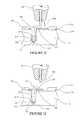
- FIG. 1Ais a schematic plan view of a semiconductor component having through wire interconnects
- FIG. 1Bis a schematic side elevation view of the semiconductor component of FIG. 1A ;
- FIG. 1Cis an enlarged schematic plan view taken along line 1 C of FIG. 1A illustrating a through wire interconnect of the semiconductor component, with a bonding member cut away to show a ball bond;
- FIG. 1Dis an enlarged schematic cross sectional view taken along section line 1 D- 1 D of FIG. 1C illustrating a through wire interconnect;
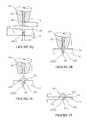
- FIG. 1Eis an enlarged schematic plan view equivalent to FIG. 1C , illustrating an alternate embodiment wedge bonded through wire interconnect on the semiconductor component;
- FIG. 1Fis an enlarged schematic cross sectional view taken along section line 1 F- 1 F of FIG. 1E illustrating the wedge bonded through wire interconnect;
- FIG. 1Gis an enlarged schematic plan view equivalent to FIG. 1C , illustrating an alternate embodiment ribbon wire through wire interconnect on the semiconductor component;
- FIG. 1His an enlarged schematic cross sectional view taken along section line 1 H- 1 H of FIG. 1G illustrating the ribbon wire through wire interconnect;
- FIG. 1Iis an enlarged schematic plan view equivalent to FIG. 1C , illustrating an alternate embodiment compressed through wire interconnect on the semiconductor component;
- FIG. 1Jis an enlarged schematic cross sectional view taken along section line 1 J- 1 J of FIG. 1I illustrating the compressed through wire interconnect;
- FIG. 1Kis an enlarged schematic plan view equivalent to FIG. 1D , illustrating an alternate embodiment wire-on-bonding-member through wire interconnect on the semiconductor component;
- FIG. 1Lis an enlarged schematic plan view equivalent to FIG. 1D , illustrating an alternate embodiment double-bump through wire interconnect on the semiconductor component;
- FIG. 1Mis an enlarged schematic plan view equivalent to FIG. 1D , illustrating an alternate embodiment cap-member through wire interconnect on the semiconductor component;
- FIGS. 2A-2Pare schematic cross sectional views illustrating steps in a method for fabricating a semiconductor component with a through wire interconnect
- FIGS. 2Q-2Tare schematic cross sectional views illustrating steps in a method for fabricating a semiconductor component with a compressed wire through wire interconnect
- FIG. 3Ais a schematic plan view taken along line 3 A- 3 A of FIG. 2A illustrating multiple semiconductor substrates on a wafer for performing a wafer level fabrication method;
- FIG. 3Bis an enlarged schematic plan view taken along line 3 B- 3 B of FIG. 28 illustrating an offset via configuration on a substrate contact;
- FIGS. 3C-3Fare enlarged schematic plan views equivalent to FIG. 3B , illustrating alternate via configurations, including multiple vias, on substrate contacts;
- FIG. 3Gis an enlarged schematic cross sectional view taken along section line 3 G- 3 G of FIG. 2D illustrating a bonding wire used in the fabrication of through wire interconnects;
- FIG. 3His an enlarged schematic cross sectional view equivalent to FIG. 3G illustrating an alternate embodiment insulated bonding wire
- FIGS. 3I and 3Jare schematic cross sectional views illustrating alternate embodiment co-axial through wire interconnects
- FIG. 4Ais a schematic cross sectional view of a semiconductor component constructed using the method of FIGS. 2A-2P ;
- FIG. 4Bis a schematic cross sectional view of a stacked semiconductor component constructed using the semiconductor component of FIG. 4A ;
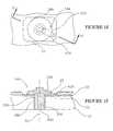
- FIG. 5is a schematic cross sectional view of a stacked wire bonded FBGA semiconductor component constructed using the stacked semiconductor component of FIG. 4B ;
- FIG. 6is a schematic cross sectional view of a stacked flip chip bonded FBGA semiconductor component constructed using the stacked semiconductor component of FIG. 4B ;
- FIG. 7is a schematic cross sectional view of a stacked redistribution layer (RDL) chip scale (CSP) semiconductor component constructed using the stacked semiconductor component of FIG. 4B with an added RDL layer;
- RDLredistribution layer
- CSPchip scale
- FIG. 8is a schematic cross sectional view of a four die stacked semiconductor component
- FIG. 9is a schematic cross sectional view of a four die stacked redistribution layer (RDL) chip scale (CSP) semiconductor component;
- RDLredistribution layer
- CSPchip scale
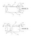
- FIG. 10is a schematic cross sectional view of a four die wire bonded stacked semiconductor component constructed
- FIG. 11is a schematic cross sectional view of a four die stacked flip chip bonded semiconductor component
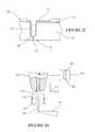
- FIG. 12is a schematic cross sectional view of a two die stacked face to face semiconductor component with terminal contacts on opposing sides;
- FIG. 13is a schematic cross sectional view of a two die stacked back to back semiconductor component with terminal contacts on opposing sides;
- FIG. 14is a schematic view illustrating a system for fabricating semiconductor components with through wire interconnects.
- semiconductor componentmeans an electronic element that includes a semiconductor substrate.
- semiconductor substratemeans an electronic element, such as a semiconductor die, or a semiconductor package that includes integrated circuits and semiconductor devices.
- Interconnectmeans an electrical element which electrically connects different electrical elements and transmits signals between these elements.
- Wafer-levelmeans a process conducted on an element, such as a semiconductor wafer, containing multiple semiconductor substrates.
- Die levelmeans a process conducted on a singulated element, such as a singulated semiconductor die or package.
- Chip scalemeans having an outline about the same as that of a semiconductor die.
- wafer sizemeans having an outline about the same as that of a semiconductor wafer.
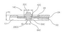
- the semiconductor component 10( FIG. 1A ) includes a semiconductor substrate 12 ( FIG. 1B ) and a plurality of through wire interconnects 14 ( FIG. 1B ) on the semiconductor substrate 12 .
- the semiconductor substrate 12can comprise a conventional semiconductor die, or a thinned semiconductor die, having integrated circuits 22 ( FIG. 1D ) constructed in a desired electrical configuration using active semiconductor devices such as transistors.
- the semiconductor substrate 12 ( FIG. 1B )can comprise a high speed digital logic device, such as a dynamic random access memory (DRAM), a static random access memory (SRAM), a flash memory, a microprocessor, a digital signal processor (DSP), or an application specific integrated circuit (ASIC).
- the semiconductor substrate 12 ( FIG. 1B )can comprise a tested die that has been certified as a known good die.
- the semiconductor substrate 12is a generally rectangular shaped die having opposed lateral edges and opposed longitudinal edges.
- the semiconductor substrate 12can have any polygonal shape, such as square or triangular, and can also have a circular or oval shape.
- the semiconductor substrate 12can comprise a full thickness semiconductor die or a thinned semiconductor die.
- the semiconductor substrate 12includes a circuit side 16 (“first side” in some of the claims), and a back side 18 (“second side in some of the claims).
- the semiconductor substrate 12includes a plurality of substrate contacts 20 on the circuit side 16 , which in the illustrative embodiment comprise the device bond pads.
- the substrate contacts 20can comprise redistribution contacts (i.e., contacts formed in conjunction with a redistribution layer (RDL)).
- the substrate contacts 20can comprise a highly-conductive, wire-bondable metal, such as aluminum or copper.
- the substrate contacts 20can also comprise stacks of different metals, such as aluminum-nickel-gold, aluminum-nickel-solder, and copper-palladium.
- the substrate contacts 20can comprise special purpose contacts formed specifically for constructing the through wire interconnects 14 .
- the substrate contacts 20can comprise electrically isolated contacts, that are not in electrical communication with the integrated circuits 22 on the semiconductor substrate 12 .
- this conceptcan be employed in stacked components to reduce unwanted capacitance, noise, bleed off voltage and bleed off current.
- the semiconductor substrate 12( FIG. 1A ) is illustrated with only four substrate contacts 20 ( FIG. 1A ) arranged in a single row.
- the semiconductor substrate 12can include tens of substrate contacts 20 ( FIG. 1A ) arranged in a desired configuration, such as a center array, an edge array or an area array.
- the substrate contacts 20( FIG. 1A ) have a generally rectangular peripheral outline and angled corners.
- the substrate contacts 20( FIG. 1A ) can have any polygonal shape including square, circular, triangular and oval.
- a size of the substrate contacts 20( FIG.
- each substrate contact 20can have a length (L) ( FIG. 1C ) of from about 50 ⁇ m to 200 ⁇ m and a width (W) ( FIG. 1C ) of from about 50 ⁇ m to 200 ⁇ m.
- each substrate contact 20has an associated through wire interconnect 14 .
- the through wire interconnects 14can also be formed on only selected substrate contacts 20 .
- only the substrate contacts 20 having a selected output or input configuratione.g., Vss, Vcc
- Vssoutput or input configuration
- the substrate contacts 20can be in electrical communication with internal conductors 24 located within the semiconductor substrate 12 proximate to the circuit side 16 .
- the internal conductors 24are in electrical communication with the integrated circuits 22 in the semiconductor substrate 12 .
- the internal conductors 24can be part of the internal structure of the semiconductor substrate 12 , and can comprise a highly conductive metal, such as aluminum or copper.
- a die passivation layer 26FIG. 1D ) proximate to the circuit side 16 protects the internal conductors 24 ( FIG. 1D ) and the integrated circuits 22 ( FIG. 1D ).
- the die passivation layer 26FIG.
- the die passivation layer 26can comprise an electrically insulating material, such as BPSG (borophosphosilicate glass), a polymer or an oxide.
- the die passivation layer 26includes openings 44 ( FIG. 1D ) aligned with the substrate contacts 20 which provide access to the substrate contacts 20 . All of the elements of the semiconductor substrate 12 including the integrated circuits 22 ( FIG. 1D ), the internal conductors 24 ( FIG. 1D ), and the die passivation layer 26 ( FIG. 1D ), can be formed using well known semiconductor fabrication processes.
- the through wire interconnect 14includes a via 28 through the substrate contact 20 and the semiconductor substrate 12 , a wire 30 in the via 28 , a bonding member 32 on the wire 30 and the substrate contact 20 , and a dielectric material 36 in the via 28 .
- the via 28( FIG. 1D ) extends through the substrate contact 20 , and through the full thickness of the semiconductor substrate 12 , from the circuit side 16 to the back side 18 thereof.
- the via 28( FIG. 1D ) is generally circular, and has an inside diameter (ID) which is about 1.5 to 3 times larger than the outside diameter (OD) of the wire 30 ( FIG. 1D ).
- IDinside diameter
- ODoutside diameter
- the wire 30FIG.
- a length of the via 28 ( FIG. 1D )is dependent on an overall thickness T of the semiconductor substrate 12 ( FIG. 1D ).
- a representative range for the thickness T of the semiconductor substrate 12 ( FIG. 1D )can be from about 10 ⁇ m to 725 ⁇ m, depending on whether the semiconductor substrate 12 is a full thickness die or wafer, or a thinned die or wafer.
- the via 28can also include an insulating layer 34 ( FIG. 1D ) formed on an inside diameter thereof, which electrically insulates the via 28 ( FIG. 1D ) from the integrated circuits 22 ( FIG. 1D ), and other electrical elements on the semiconductor substrate 12 .
- the insulating layer 34 ( FIG. 1D )can comprise an electrically insulating material, such as a polymer (e.g., polyimide or parylene) or an oxide (e.g., SiO 2 ).
- the wire 30( FIG. 1D ), rather than the via 28 ( FIG. 1D ), or in addition to the via 28 ( FIG. 1D ), can be electrically insulated.
- the via 28is illustrated as being located in an upper left hand corner of the substrate contact 20 .
- the via 28is offset in both x and y directions from a center of the substrate contact 20 .
- the via 28can have an inside diameter (ID) ( FIG. 1D ) that is about one half of the width (L) ( FIG. 1C ) of the substrate contact 20 ( FIG. 1C ).
- IDinside diameter
- a via 28 Acan be located in the center 48 ( FIG. 3C ) of the substrate contact 20 .
- multiple vias 28 B ( FIG. 3D ), 28 C ( FIG. 3E ) or 28 D ( FIG. 3F )can be formed in the same substrate contact 20 .
- the wire 30is located along a longitudinal axis 70 ( FIG. 2E ) of the via 28 , and extends across the entire length of the via 28 .
- the wire 30 ( FIG. 1D )can be held in place in the via 28 ( FIG. 1D ) by the dielectric material 36 ( FIG. 1D ), which fills the via 28 ( FIG. 1D ) and surrounds the wire 30 ( FIG. 1D ).
- the wire 30 ( FIG. 1D )has a first end 38 ( FIG. 1D ) extending out of the via 28 ( FIG. 1D ) and bonded to the substrate contact 20 ( FIG. 1D ), and a second end 40 ( FIG. 1D ) extending just outside of the via 28 proximate to the back side 18 ( FIG. 1D ) of the semiconductor substrate 12 .
- the through wire interconnect 14( FIG. 1D ) also includes a bonded connection 42 ( FIG. 1D ) between the first end 38 ( FIG. 1D ) of the wire 30 and the substrate contact 20 .
- the second end 40 ( FIG. 1D ) of the wire 30can comprise a generally spherically shaped contact ball 64 , such as a “free air ball” formed using an electronic flame off (EFO) process to be hereinafter described.
- EFOelectronic flame off
- the bonded connection 42( FIG. 1D ) comprises a ball bond formed using a wire bonding process, such as thermosonic wire bonding.
- a through wire interconnect 14 A( FIGS. 1E and 1F ) can include a bonded connection 42 A ( FIGS. 1E and 1F ) in the form of a wedge bond formed using ultrasonic wire bonding.
- a through wire interconnect 14 B( FIGS. 1G and 1H ) can include a ribbon wire 30 B ( FIGS. 1G and 1H ) such as a bonding ribbon, and a bonded connection 42 B ( FIGS. 1G and 1H ) can comprise a ribbon wire bond.
- a through wire interconnect 14 Ccan include a compressed wire 30 C ( FIGS. 1I and 1J ), and a bonded connection 42 C ( FIGS. 1I and 1J ) can be in the form of a stud bump and a compression flange on the compressed wire 30 C ( FIGS. 1I and 1J ).
- a representative outside diameter (OD) ( FIG. 1D ) of the wire 30can be from about 12 ⁇ m to about 150 ⁇ m.
- the wire 30 ( FIG. 1D )can comprise a conventional wire material used in semiconductor packaging, such as solder alloys, gold, gold alloys, copper, copper alloys, silver, silver alloys, aluminum, aluminum-silicon alloys, and aluminum-magnesium alloys.
- the wire 30 ( FIG. 1D )can comprise a metal, or a metal alloy, that does not contain reductions of hazardous substances (ROHS), such as lead.
- ROHS free metalsinclude lead free solders, such as 97.5% Sn 2.5% Ag.
- Other ROHS free metalsinclude gold, copper and alloys of these metals such as copper coated with a layer of flash gold.
- the melting point of the wire 30 ( FIG. 1D )should preferably be greater than that of the substrate contact 20 .
- the bonding member 32is located next to the via 28 , and is bonded to the substrate contact 20 in a right, lower quadrant of the substrate contact 20 .
- the bonding member 32( FIG. 1D ) can be centered on the substrate contact 20 ( FIG. 1D ) and on the via 28 ( FIG. 1D ), or located on any portion of the substrate contact 20 ( FIG. 1D ) or the via 28 ( FIG. 1D ).
- the bonding member 32 ( FIG. 1D )bonds portions of the wire 30 ( FIG. 1D ) to the substrate contact 20 ( FIG. 1D ).
- the bonding member 32( FIG.
- the bonding member 32( FIG. 1D ) preferably comprises a non oxidizing, bondable material such as gold or platinum, or a reflow material, such as solder.
- the bonding member 32( FIG. 1D ) comprises a stud bump, or a ball bump, bonded to the substrate contact 20 .
- the bonding member 32( FIG. 1D ) can be formed using a wire bonder, a stud bumper, or a ball bumper.
- the bonding member 32 ( FIG. 1D )can comprise a solder joint, a welded connection, or a conductive polymer connection, formed using a bonding process, such as thermal or pressure bonding to the substrate contact 20 .
- a bonding processsuch as thermal or pressure bonding to the substrate contact 20 .
- the bonding member 32has a diameter which is less than the length (L) and the width (W) of the substrate contact 20 (e.g., 25% to 75%), such that it covers only a portion of the substrate contact 20 , and does not cover the via 28 .
- a bonding member 32 Acan also be configured to substantially cover the substrate contact 20 and the via 28 .
- an alternate embodiment wedge bonded through wire interconnect 14 Ais substantially similar to the through wire interconnect 14 ( FIG. 1D ), but includes a wire 30 A ( FIG. 1F ) that is wedge bonded to the substrate contact 20 .
- a bonded connection 42 A ( FIG. 1F ) between the wire 30 A ( FIG. 1F ) and the substrate contact 20comprises a wedge bond formed using an ultrasonic bonding process.
- the through wire interconnect 14 A ( FIG. 1F )includes a bonding member 32 A, which is substantially similar to the bonding member 32 ( FIG. 1D ). However, the bonding member 32 A ( FIG. 1E ) covers almost all of the surface of the substrate contact 20 ( FIG.
- the through wire interconnect 14 Aalso includes a dielectric material 36 A ( FIG. 1F ) in the via 28 A which secures and electrically insulates the wire 30 A ( FIG. 1F ).
- the through wire interconnect 14 Aalso includes a contact 64 A which comprises an exposed planar surface on an end of the wire 30 A.
- an alternate embodiment ribbon wire through wire interconnect 14 Bis substantially similar to the through wire interconnect 14 ( FIG. 1D ), but includes a ribbon wire 30 B ( FIG. 1G ) in the form of a bonding ribbon. Further, a bonded connection 42 B ( FIG. 1H ) between the ribbon wire 30 B ( FIG. 1G ) and the substrate contact 20 comprises a wedge bond formed using a ribbon wire bonding process.
- the through wire interconnect 14 B ( FIG. 1G )includes a bonding member 32 B ( FIG. 1H ), which is substantially similar to the bonding member 32 ( FIG. 1D ). Further, the through wire interconnect 14 B ( FIG. 1G ) includes a slot via 28 S (FIG.
- the through wire interconnect 14 B( FIG. 1G ) also includes a dielectric material 36 B ( FIG. 1H ) in the slot via 28 A ( FIG. 1G ), which secures and electrically insulates the ribbon wire 30 B ( FIG. 1G ).
- the through wire interconnect 14 Balso includes a contact 64 B which comprises an exposed surface of the ribbon wire 30 B.
- the ribbon wire 30 B( FIG. 1G ) can have a selected size from fine ribbon wire [13 ⁇ m ⁇ 51 ⁇ m (0.5 ⁇ 2 mil)] to heavy ribbon wire [25.4 ⁇ m ⁇ 254 mm (1 ⁇ 10 mil)].
- the ribbon wire 30 B ( FIG. 1G )can comprise a conventional material such as gold, aluminum, silver or palladium.
- the ribbon wire 30 B ( FIG. 1G )provides several advantages over round wire including high reliability bonded connections 42 B ( FIG. 1G ), a high pull strength due to more surface contact, less cratering, minimal wire sway, longer wire spans, and a planar bonding surface for the bonding member 32 B ( FIG. 1H ).
- the ribbon wire 30 B( FIG. 1G ) provides a low impedance and a low inductance due to the skin effect at high frequency (i.e., current density concentration in the surface layers of the conductors increases with frequency). Due to the skin effect, the surface area of the ribbon wire 30 B ( FIG. 1G ) provides a larger surface area for current carrying relative to round wire.
- Automatic ribbon bondersare available from Kulicke & Soffa Industries, Inc. of Willow Grove, Pa.
- an alternate embodiment compressed wire through wire interconnect 14 Cis substantially similar to the through wire interconnect 14 ( FIG. 1D ), but includes a compressed wire 30 C ( FIG. 1J ) such as a stud bump, wedged into a via 28 CO.
- the substrate 12has a thickness TC that is ultra thin (e.g., 10-100 ⁇ m).
- a depth of the via 28 COcan be only slightly greater than an initial diameter of the compressed wire 30 C.
- a bonding member 32 C( FIG. 1J ) is formed integrally with the compressed wire 30 C ( FIG. 1J ), and a bonded connection 42 C ( FIG.
- the compressed wire through wire interconnect 14 C( FIG. 1J ) also includes a contact 64 C which comprises an exposed surface of the compressed wire 30 C.
- an alternate embodiment wire-on-bonding-member through wire interconnect 14 Dis substantially similar to the through wire interconnect 14 ( FIG. 1D ), but includes a wire 30 D bonded to a top portion of a bonding member 32 D.
- a bonded connection 42 Dis formed between the wire 30 D and a top portion of the bonding member 32 D.
- the bonding member 32 Dcould comprise a stud bump bonded to the substrate contact 20
- the bonded connection 42 Dcould comprise a ball bond formed on the stud bump.
- the bonded connection 42 Dcan be formed anywhere on the bonding member 32 D such as in the center, or on an exterior surface thereof.
- an alternate embodiment double-bump through wire interconnect 14 Eis substantially similar to the through wire interconnect 14 ( FIG. 1D ), but includes a double bump 32 E.
- a bonded connection 42 Ecomprises a wire 30 E within the double bump 32 E sandwiched between the stacked bumps of the double bump 32 E.
- the bonded connection 42 Ecan be formed between the lowermost bump of the double bump 32 E and the substrate contact 20 .
- an alternate embodiment cap-member through wire interconnect 14 Fis substantially similar to the through wire interconnect 14 ( FIG. 1D ), but includes a cap member 33 F that encapsulates a bonding member 32 F and a bonded connection 42 F between a wire 30 F and the substrate contact 20 .
- the cap member 33 Fcan comprise an electrically conductive material such as solder or a conductive polymer.
- the cap member 33 Fcan be used as an electrically conductive bonding structure for fabricating stacked components.
- FIGS. 2A-2Psteps in a method for fabricating the component 10 ( FIG. 1A ) with through wire interconnects 14 ( FIG. 1A ) is illustrated.
- the semiconductor substrate 12is provided substantially as previously described, with the substrate contact 20 , the passivation layer 26 and the internal conductor 24 in electrical communication with the integrated circuits 22 ( FIG. 1D ).
- the substrate contact 20can be electrically isolated. This concept will be further explained as the description proceeds.
- the methodis performed at the wafer level on a semiconductor wafer 46 ( FIG. 3A ) containing a plurality of semiconductor substrates 12 .
- the method of the inventioncan be performed at the die level on singulated substrates, such as singulated bare dice and known good dice (KGD).
- the semiconductor wafer 46FIG. 3A
- the semiconductor wafer 46comprises a semiconductor material, such as silicon or gallium arsenide.
- the semiconductor substrates 12are in the form of semiconductor dice having a desired electrical configuration, such as memory, application specific, or imaging and image sensing.
- the method of the inventioncan be performed on other substrates including ceramic, plastic, tape, printed circuit board (PCB), metal lead frame, or flex circuit substrates.
- the semiconductor substrate 12includes the circuit side 16 with the substrate contacts 20 and die passivation layer 26 thereon, and the back side 18 .
- the vias 28are formed through the substrate contacts 20 , but only part way through the substrate 12 .
- the vias 28can be formed using an etching process, a laser machining process, an ion milling process, a mechanical process (e.g., drilling, grinding, abrasion), or combinations of any of these processes.
- the vias 28can be formed using a dry etch process, such as a reactive ion etching (RIE) through a mask, such as a photo mask or a hard mask, having openings, which locate the vias 28 on the substrate contacts 20 .
- RIEreactive ion etching
- a first etch gascan be used to etch through the substrate contacts 20
- a second etch gascan be used to etch part way through the semiconductor substrate 12
- parameters (e.g., time, temperature, etchant) of the dry etch processcan be controlled such that a depth “D” of the vias 28 ( FIG. 2B ) is endpointed within the semiconductor substrate 12 at a distance “S” ( FIG. 2B ) from the back side 18 .
- RIEreactive ion etching
- Reactive ion etching (RIE)is sometimes referred to as “BOSCH” etching, after the German company Robert Bosch, which developed the original process.
- FIG. 2BAnother method for forming the vias 28 ( FIG. 2B ) combines etching and laser machining processes.
- an etch mask(not shown) and an etching process can be used to form the vias 28 through the substrate contacts 20 .
- a wet etchantcan be used.
- substrate contacts 20 made of aluminumone suitable wet etchant is H 3 PO 4 .
- a laser machining processcan be used to form the vias 28 part way through the semiconductor substrate 12 .
- One suitable laser system for performing the laser machining stepis manufactured by XSIL LTD of Dublin, Ireland, and is designated a Model No. XISE 200.
- TMAHtetramethylammoniumhydroxide
- the vias 28are offset in x and y directions from the centers 48 of the substrate contacts 20 .
- This arrangementprovides the most surface area on the substrate contacts 20 available for subsequently forming the bonded connections 42 ( FIG. 1C ).
- the vias 28 Acan alternately be formed through the centers 48 of the substrate contacts 20 .
- the bonded connections 42 A( FIG. 1F ) can be radially offset from the centers 48 of the substrate contacts 20 .
- two vias 28 Bcan also be formed on each substrate contact 20 for forming two through wire interconnects on each substrate contact 20 .
- FIG. 3Bin the illustrative embodiment the vias 28 are offset in x and y directions from the centers 48 of the substrate contacts 20 .
- This arrangementprovides the most surface area on the substrate contacts 20 available for subsequently forming the bonded connections 42 ( FIG. 1C ).
- the vias 28 Acan alternately be formed through the centers 48 of the substrate contacts 20 .
- the bonded connections 42 A( FIG. 1F ) can be
- three vias 28 Ccan also be formed on each substrate contact 20 for forming three through wire interconnects on each substrate contact 20 .
- four vias 28 Dcan also be formed on each substrate contact 20 for forming four through wire interconnects on each substrate contact 20 .
- the insulating layers 34can be formed in the vias 28 .
- the insulating layers 34can comprise a polymer, such as polyimide or parylene, deposited using a suitable process, such as vapor deposition, capillary injection or screen-printing.
- the insulating layers 34can comprise a deposited oxide layer, such as a low temperature deposited oxide.
- the insulating layers 34can comprise a grown oxide layer, such as silicon dioxide formed by oxidation of silicon.
- a vent 50can be formed from the back side 18 of the semiconductor substrate 12 into each via 28 .
- the vents 50can be formed using a laser machining process, and the previously described laser systems. Alternately, the vents 50 ( FIG. 2C ) can be formed using an etching process performed from the back side 18 of the semiconductor substrate 12 .
- the vents 50FIG. 2C ) allow the wire 30 ( FIG. 1D ) and the dielectric material 36 ( FIG. 1D ) to be more easily placed in the via 28 ( FIG. 2C ).
- the vents 50provide a pressure differential for venting trapped gases from the via 28 during placement of the wire 30 ( FIG.
- vents 50help to draw and seat the wires 30 ( FIG. 1D ) in vias 28 .
- the vents 50( FIG. 1D ) also provide capillary action under a vacuum for depositing the dielectric material 36 into the vias 28 .
- the vents 50( FIG. 2C ) have a diameter that is less than the diameter of the wires 30 ( FIG. 1D ).
- the diameter of the vents 50( FIG. 2C ) can be selected to provide seats for the second ends 40 of the wires 30 .
- a representative diameter of the vents 50 ( FIG. 2C )can be from 5 ⁇ m to 15 ⁇ m.
- the vents 50are tapered from the back side 18 of the semiconductor substrate 12 , as would occur with a laser machining process, wherein lasered openings are larger at the point of entry.
- a wire bonder 52 having a bonding capillary 54can be provided.
- the wire bonder 52is configured to perform an ultra fine pitch (e.g., ⁇ 65 ⁇ m) wire bonding process.
- Suitable wire bondersare manufactured by Kulicke & Soffa Industries Inc. of Willow Grove, Pa., and Palomar of Carlsbad, Calif.
- One suitable wire bonderis a model “8098” large area ball bonder manufactured by Kulicke & Soffa Industries Inc., having a total bond placement accuracy of about +/ ⁇ 5 ⁇ m at pitches down to about 65 ⁇ m. Bonding capillaries are available from SPT (Small Precision Tools) of Petaluma, Calif., and from Kulicke & Soffa Industries Inc.
- the wire bonder 52 ( FIG. 2D ) and the bonding capillary 54are configured to form a continuous length of bonding wire 58 into the wire 30 ( FIG. 1D ) for the through wire interconnect 14 ( FIG. 1D ).
- the bonding wire 58can comprise a conventional wire material used in semiconductor packaging, such as the previously identified materials for the wire 30 ( FIG. 1D ).
- the bonding wire 58can be generally circular in cross section with an outside diameter (OD) selected to allow placement of the wire 58 into the via 28 .
- a representative range for the outside diameter (OD) of the bonding wire 58can be from about 12 ⁇ m to about 150 ⁇ m. As shown in FIG.
- an alternate embodiment insulated bonding wire 58 Aincludes an electrically insulating outer layer 78 , such as a polymer.
- the insulating layer 78 on the bonding wire 58can take the place of the insulating layers 34 ( FIG. 1D ) in the vias 28 ( FIG. 1D ).
- This type of bonding wire 58 Ais available from Micro Bond of Canada.
- the insulated bonding wire 58 Acan be used to form a co-axial through wire interconnect 14 CA- 1 .
- the co-axial through wire interconnect 14 CA- 1( FIG. 3I ) includes a via 28 CA ( FIG. 3I ) through the substrate contact 20 and an insulating layer 34 CA ( FIG. 3I ) on the via 28 CA ( FIG. 3I ) substantially as previously described for the via 28 ( FIG. 1D ) and the insulating layer 34 ( FIG. 1D ).
- the co-axial through wire interconnect 14 CA- 1also includes a dielectric material 36 CA, which secures the insulated bonding wire 58 A ( FIG. 3I ) in the via 28 CA ( FIG.
- the co-axial through wire interconnect 14 CA- 1also includes a co-axial conductor 31 CA ( FIG. 3I ), which comprises an additional metal layer on the insulating layer 34 CA ( FIG. 3I ).
- the co-axial conductor 31 CA ( FIG. 3I )forms a shield which confines radiation formed by a transverse electromagnetic (TEM) wave during transmission of electromagnetic signals through the wire 58 A ( FIG. 3I ).
- the co-axial through wire interconnect 14 CA- 1 ( FIG. 3I )can also be used to transmit first signals through the wire 58 A ( FIG. 3I ), and to transmit second signals through the co-axial conductor 31 CA ( FIG. 3I ).
- an alternate embodiment co-axial through wire interconnect 14 CA- 2is substantially similar to the co-axial through wire interconnect 14 CA- 1 ( FIG. 3I ), but includes the wire 30 (un-insulated as previously described), and an additional insulating layer 35 CA on the co-axial conductor 31 CA ( FIG. 3J ).
- the co-axial conductor 31 CAforms a shield which confines radiation formed by a transverse electromagnetic (TEM) wave during transmission of electromagnetic signals through the wire 30 ( FIG. 3I ).
- the co-axial through wire interconnect 14 CA- 2( FIG. 3J ) also allows first signals to be transmitted through the wire 30 ( FIG. 3J ), and second signals to be transmitted through the co-axial conductor 31 CA ( FIG. 3I ).
- the bonding capillary 54is movable in x, y and z directions responsive to signals from a controller 80 of the wire bonder 52 .
- the bonding capillary 54includes an elongated opening 60 having an inside diameter about twice the diameter of the bonding wire 58 , and an enlarged, chamfered terminal portion.
- the wire bonder 52also includes wire clamps (not shown) operably associated with the bonding capillary 54 , which are configured to open and close about the bonding wire 58 responsive to signals from the controller 80 .
- U.S. patent application Ser. No. 11/102,408, filed on Apr. 8, 2005, which is incorporated herein by reference,provides further details of the wire bonder 52 and the bonding process to be hereinafter described.
- the wire bonder 52also includes an electronic flame off (EFO) wand 56 configured to generate an electronic spark 62 for forming the contact ball 64 on a terminal portion of the bonding wire 58 .
- EFOelectronic flame off
- the contact ball 64will subsequently form the first end 38 ( FIG. 1D ) of the wire 30 .
- the contact ball 64is also known in the art as a “free air ball” (FAB).
- a diameter of the contact ball 64will be dependent on the diameter of the bonding wire 58 , with from 1.5 to 4 times the diameter of the bonding wire 58 being representative.
- an alignment stepcan be performed in which the bonding capillary 54 is aligned with the via 28 .
- the alignment stepcan be performed using an automated alignment system 82 ( FIG. 2D ) of the wire bonder 52 ( FIG. 2D ).
- the semiconductor wafer 46 ( FIG. 3A ) with the semiconductor substrates 12 thereoncan be placed on a work holder 68 ( FIG. 2E ) of the wire bonder 52 ( FIG. 2D ).
- the position of the via 28FIG.
- the bonding capillary 54can be operated to position the bonding wire 58 such that a terminal portion of the bonding wire 58 has a desired tail length TL ( FIG. 2E ).
- the tail length TLcan be selected to be slightly greater (e.g., 1 to several microns) than the depth D ( FIG. 2B ) of the via 28 ( FIG. 2E ).
- a placing stepcan be performed in which the bonding capillary 54 is moved in a z-direction, as indicated by arrow 76 , to place the tail length TL of the bonding wire 58 into the via 28 .
- the placing stepcan be performed such that the contact ball 64 contacts a bottom surface 74 ( FIG. 2F ) of the via 28 .
- the vent 50FIG. 2F ) helps to maintain a positive air or gas flow through the via 28 , which facilitates placement of the tail length TL ( FIG. 2E ) of the bonding wire 58 into the via 28 .
- the vent 50can be formed with a surface which seats the contact ball 64 on the bottom surface 74 ( FIG.
- the placing stepcan be performed by maintaining the bonding capillary 54 in a stationary position over the via 28 , and then spooling the bonding wire 58 into the via 28 .
- a looping stepcan be performed in which the wire clamps (not shown) of the wire bonder 52 ( FIG. 2D ) are opened, and the bonding capillary 54 is moved in x and z directions (and also in the y direction if required) into a position on the substrate contact 20 for making the bonded connection 42 ( FIG. 2H ).
- the looping stepcan be performed using the alignment system 82 ( FIG. 2D ) of the wire bonder 52 ( FIG. 2D ).
- the controller 80 ( FIG. 2D ) of the wire bonder 52 ( FIG. 2D )can be loaded with information on the desired locations of the bonded connections 42 ( FIG. 2H ).
- a bonding stepcan be performed in which the bonded connection 42 is formed on the substrate contact 20 .
- the bonded connection 42comprises a ball bond formed using thermosonic by the bonding capillary 54 .
- the bonded connection 42can comprise a wedge bond, a ribbon wire bond, or a flanged portion of the bonding member 32 .
- the bonded connection 42can also comprise a reflow, welded, metallurgical, mechanical or polymer connection formed using any suitable process known in the art.
- FIGS. 2I and 2Ja severing step can be performed in which the wire clamps of the wire bonder 52 ( FIG. 2D ) are closed, and the bonding capillary 54 is moved as indicated by arrow 84 ( FIG. 2I ) to sever the bonding wire 58 from the bonded connection 42 .
- FIG. 2Jillustrates the resultant wire 30 of the through wire interconnect 14 ( FIG. 1D ).
- the wire 30( FIG. 2J ) includes the first end 38 ( FIG. 2J ) having the bonded connection 42 ( FIG. 2J ) in the form of a ball bond on the substrate contact 20 .
- the wire 30 ( FIG. 2J )also includes the second end 40 ( FIG. 2J ) having a contact in the form of the contact ball 64 , which is preferably seated in the via 28 in contact with the bottom surface 74 thereof.
- a dielectric fill stepcan be performed in which the dielectric material 36 is deposited into the via 28 in viscous form and then cured to harden.
- the dielectric material 36can comprise an electrically insulating curable polymer, such as a polyimide, an epoxy or a silicone.
- the dielectric material 36( FIG. 2K ) can include fillers, such as silicates, configured to reduce the coefficient of thermal expansion (CTE) and adjust the viscosity of the dielectric material. Suitable curable polymers are manufactured by Shinitsu of Japan, and Dexter Electronic Materials of Rocky Hill, Conn.
- the dielectric material 36( FIG. 2K ) provides a potting structure which secures and electrically insulates the wire 30 in the via 28 .
- the dielectric material 36( FIG. 2K ) can be injected into the via 28 in a viscous state, pulled by capillary action by vacuum directed through the vent 50 , and then cured.
- a positive displacement mechanismsuch as a syringe, can be used to dispense a quantity of the dielectric material 36 ( FIG. 2K ) into the via 28 .
- One suitable nozzle deposition apparatusalso known as a material dispensing system, is manufactured by Asymtek of Carlsbad, Calif.
- Other suitable deposition processes for depositing the dielectric material 36 ( FIG. 2K ) into the via 28include screen printing, stenciling and stereographic lithography.
- a dielectric removal stepcan be performed to substantially remove the dielectric material 36 from the substrate contact 20 .
- the dielectric removal stepcan be performed using an etch process, such as reactive ion etching (RIE), plasma etching or wet etching. With an etch process an etchant, strips or cleans the excess dielectric material 36 from the substrate contact 20 .
- RIEreactive ion etching
- etchantan etchant
- a bonding member forming stepcan be performed in which the bonding member 32 is formed on the substrate contact 20 and on a portion of the wire 30 .
- the bonding member forming stepcan be performed to position the bonding member 32 on a desired portion of the substrate contact 20 .
- the bonding member 32can be offset with respect to the via 28 or centered on the via 28 .
- a bonding member 32 Acan cover the entire substrate contact 20 .
- the bonding member 32( FIG. 2M ) comprises a non oxidizing easily bondable material, such as gold or platinum.
- the bonding member 32in addition to providing an external bonding element for the through wire interconnect 14 ( FIG. 1D ), also secures the wire 30 in the via 28 , and provides a security bond for the bonded connection 42 .
- the bonding member 32comprises a stud bump or a ball bump, formed using a wire bonder, a stud bumper or a ball bumper.
- a bonding capillary similar to the bonding capillary 54can be used to form a stud bump.
- a suitable stud bumperis a “WAFER PRO PLUS” high speed large area stud bumper manufactured by Kulicke & Soffa Industries Inc. of Willow Grove, Pa.
- suitable solder ball bumpersare manufactured by Pac Tech Packaging Technologies of Falkensee, Germany.
- the bonded connection 42has been made, and the bonding member 32 has been placed on the bonded connection 42 .
- the bonding member 32can also be bonded to the substrate contact 20 first, and then the end 38 of the wire 30 bonded to the bonding member 32 second.
- the bonded connection 42can also be located on any portion of the bonding member 32 , such as on the top surface thereof, rather than on the lower surface thereof as in FIG. 2M .
- the through wire interconnect 14 D( FIG. 1K ) illustrates one such arrangement wherein the bonded connection 42 D is formed on the bonding member 32 D. Double bumping or stacked bumping techniques can also be used to form the bonding member 32 .
- the through wire interconnect 14 EFIG. 1L
- the double bump bonding member 32 EFIG. 1L ).
- a backside thinning stepcan be performed in which the semiconductor substrate 12 is thinned from the back side 18 , such that the via 28 is opened, and the contact ball 64 is exposed.
- the backside thinning stepcan be performed to expose any portion of the wire 30 which can be used as a contact for making an electrical connection from the outside to the through wire interconnect 14 .
- the backside thinning stepcan be performed such that the thinned substrate 12 has a thickness of T.
- a representative range for the thickness Tcan be from about 10 ⁇ m to 725 ⁇ m.
- temporary carriers made of glasscan be fused by heat and adhesives to the semiconductor wafer 46 ( FIG. 3A ) to protect the circuit side 16 ( FIG. 3A ) of the semiconductor substrate 12 .
- Suitable, temporary carriersare manufactured by 3-M Corporation of St. Paul, Minn., and others as well.
- the circuit side 16 of the wafer 46 ( FIG. 3A )can be protected by a removable material such as a tape or mask material applied to the semiconductor wafer 46 .
- the backside thinning step of FIG. 2Ncan be performed using a chemical mechanical planarization (CMP) apparatus.
- CMPchemical mechanical planarization
- One suitable CMP apparatusis manufactured by “ACCRETECH” of Tokyo, Japan, and is designated a model no. “PG300RM”. Suitable CMP apparatus are also commercially available from Westech, SEZ, Plasma Polishing Systems, TRUSI and other manufacturers.
- the backside thinning stepcan also be performed using an etching process, such as a wet etching process, a dry etching process or a plasma etching process.
- a combination of planarization and etchingcan be performed.
- a mechanical grindercan be used to remove the bulk of the material, followed by etching to remove grind damage.
- U.S. Pat. No. 6,908,784which is incorporated herein by reference, further describes processes and equipment for performing the backside thinning step.
- an optional back side insulating stepcan be performed in which an insulating layer 86 is formed on the thinned backside 18 of the semiconductor substrate 12 .
- the insulating layer 86can comprise a polymer layer such as polyimide or parylene, a glass such as BPSG, or an oxide such as silicon dioxide.
- the insulating layercan be formed using a suitable deposition process such as CVD, screen printing or taping. Further, the insulating layer 86 includes openings 88 which align with the contact balls 64 .
- an optional polymer button forming stepcan be performed in which polymer buttons 90 are formed on the contact balls 64 .
- the button forming stepcan be performed using a suitable polymer, such as a silicone, a polyimide or an epoxy, and a process such as nozzle deposition or screen printing.
- the polymer buttons 90can provide electrical insulation and protection, an adhesive connection, or an electrical connection. If no electrical contact is made to the contact ball 64 ( FIG. 2P ), the polymer buttons 90 can comprise an electrically insulating material.
- the polymer buttons 90( FIG. 2P ) can comprise an electrically conductive material, such as an anisotropic adhesive.
- the adhesive buttons 90can also comprise an adhesive material for applications such as stacking and surface mounting.
- a singulating stepsuch as sawing, scribing, liquid jetting, or laser cutting through a liquid, can be performed to singulate a chip scale semiconductor component 92 ( FIG. 4A ) from the wafer 46 .
- a wafer sized componentcan be provided which contains multiple unsingulated semiconductor substrates 12 .
- FIGS. 2Q-2Tsteps in a method for forming the compressed wire through wire interconnect 14 C ( FIG. 1J ) are illustrated.
- the substrate 12 , the substrate contact 20 and the bonding capillary 54are provided, as previously described.
- the via 28 COis formed in the substrate 12 as previously described.
- the depth d of the via 28 COis very small, on the order of from 10 ⁇ m to 125 ⁇ m.
- the outside diameter OD of the contact ball 64 of the bonding wire 58is approximately equal to the depth d of the via 28 CO, and to the inside diameter ID of the via 28 CO.
- the bonding capillary 58is operated to compress the contact ball 64 and the bonding wire 58 into the via 28 CO, forming the compressed wire 30 C, the bonded connection 42 C ( FIG. 2S ) and the bonding member 32 C ( FIG. 2S ).
- the contact 64 C on the compressed wire 30 Cis exposed.
- the compressed through wire interconnect 14 Ccan be fabricated by depositing a metal into the via 28 CO and then compressing the metal using a tamping tool.
- a chip scale semiconductor component 92includes the semiconductor substrate 12 having a plurality of through wire interconnects 14 , which correspond to the locations of the substrate contacts 20 .
- the substrate contacts 20can have any desired configuration including dense area arrays, such as edge arrays, center arrays, or perimeter arrays.
- the through wire interconnects 14can be used as terminal contacts, which can be surface mounted to a supporting substrate, or stacked to other components.
- the bonding members 32provide electrical connection points proximate to the circuit side 16
- the contact balls 64provide electrical connection points proximate to the back side 18 of the semiconductor substrate 12 .
- a stacked semiconductor component 94includes the semiconductor component 92 , and a bumped semiconductor die 96 stacked on the semiconductor component 92 .
- the bumped semiconductor die 96can comprise a full or partial thickness die, having a plurality of bumped contacts 98 (e.g., stud bumps or ball bumps) on a circuit side 102 thereof, in electrical communication with the integrated circuits contained on the semiconductor die 96 .
- the bumped contacts 98can be arranged in an area array, which corresponds to the area array of the through wire interconnects 14 on the semiconductor component 92 .
- the bumped contacts 98can be bonded to the contact balls 64 of the through wire interconnects 14 on the semiconductor component 92 .
- the bumped contacts 98can comprise a bondable metal such as gold, platinum or solder, or a conductive polymer, such as metal filled epoxy, which can be bonded to the contact balls 64 using a suitable process such as diffusion bonding, thermal bonding or reflow bonding.
- the bumped contacts 98can comprise gold stud bumps, and the contact balls 64 can comprise gold free air balls, such that a gold to gold diffusion bond can be formed.
- an adhesive layer 100( FIG. 4B ), such as a curable polymer underfill material, adhesively bonds the circuit side 102 ( FIG. 4B ) of the semiconductor die 96 ( FIG. 4B ) to the back side insulating layer 86 on the semiconductor component 92 .
- the stacked semiconductor component 94( FIG. 4B ) can be fabricated at the wafer level with a plurality of semiconductor dice 96 contained on a wafer, and the singulated components 92 then bonded to the semiconductor dice 96 on the wafer.
- a die attacher or an aligner bondercould be employed to place and bond the semiconductor components 92 to the semiconductor dice 96 contained on the wafer.
- the components 92can be tested prior to the bonding process and certified as known good components (KGC) to improve the yield of the bonding process.
- KGCknown good components
- the stacked semiconductor components 94could be singulated from the wafer containing the semiconductor dice 96 with the semiconductor component 92 bonded thereto.
- the semiconductor dice 96 and the semiconductor components 92could both be singulated components.
- a wafer to wafer fabrication processcould be employed wherein both the semiconductor dice 96 and the semiconductor components 92 are contained on mating wafers.
- the substrate contacts 20 ( FIG. 4B ) on the stacked semiconductor component 94 ( FIG. 4B )can be electrically isolated, and not in electrical communication with the integrated circuits 22 ( FIG. 1D ) on the semiconductor substrate 12 .
- electrical signalscan be transmitted through the stacked semiconductor component 94 ( FIG. 4B ) without adding unwanted inductance or capacitance.
- the semiconductor substrate 12 ( FIG. 4B ) of the semiconductor component 92 ( FIG. 4B )can comprise a dynamic random access memory (DRAM).
- DRAMdynamic random access memory
- the DQ circuits on some DRAM'shave up to 1 pf of capacitance added into the DQ circuits, to help offset the inductance added to the DRAM by wire bonds. In general, wire bonds have a high inductance but very low capacitance.
- capacitancecould potentially be added each time a signal is transmitted through a substrate contact 20 ( FIG. 4B ) associated with a DQ circuit.
- noise, bleed off voltage, and bleed off currentcould potentially be added to the signals transmitted through the through wire interconnects 14 ( FIG. 4B ).
- selected substrate contact 20are electrically isolated from the integrated circuits 22 ( FIG. 1D ) as required, parasitics could be reduced.
- One method for electrically isolating a substrate contact 20would be to etch or laser machine a trench around the perimeter of the substrate contact 20 ( FIG. 4B ).
- Another methodwould be to incorporate programmable links, such as fuses, antifuses or gates, between the substrate contacts 20 ( FIG. 1D ) and the integrated circuits 22 ( FIG. 1D ). Yet another method would be to design and fabricate the substrate contact 20 as an electrically isolated pass through contact for stacking applications.
- programmable linkssuch as fuses, antifuses or gates
- a wire bonded fine ball grid array (FBGA) semiconductor component 104includes the stacked semiconductor component 94 wire bonded in a board on chip (BOC) configuration to a package substrate 106 .
- the package substrate 106includes a plurality of terminal contacts 108 , such as solder balls, in a fine ball grid array.
- the terminal contacts 108are in electrical communication with wire bonding pads 118 on the package substrate 106 .
- the package substrate 106includes a wire bonding opening 116 , and a plurality of wires 110 that are wire bonded to the wire bonding pads 118 on the package substrate 106 , and to the bonding members 32 on the through wire interconnects 14 of the semiconductor component 92 .
- the wire bonded fine ball grid array (FBGA) semiconductor component 104also includes a package encapsulant 112 on the package substrate 106 , which encapsulates the stacked semiconductor component 94 , and a wire bond encapsulant 114 , which encapsulates the wires 110 and associated wire bonds.
- FBGAwire bonded fine ball grid array
- a flip chip bonded (FCIP) fine ball grid array (FBGA) semiconductor component 120includes the stacked semiconductor component 94 flip chip bonded in a chip on board (COB) configuration to a package substrate 122 .
- the package substrate 122includes a plurality of terminal contacts 124 , such as solder balls, in a fine ball grid array.
- the terminal contacts 124are in electrical communication with flip chip bonding pads 128 on the package substrate 122 .
- the bonding members 32 on the through wire interconnects 14 of the semiconductor component 92are flip chip bonded to the flip chip bonding pads 128 on the package substrate 122 .
- the semiconductor component 120also includes the package encapsulant 112 on the package substrate 122 , which encapsulates the stacked semiconductor component 94 .
- a redistribution layer (RDL) chip scale (CSP) semiconductor component 130is substantially similar to the stacked semiconductor component 94 ( FIG. 4B ). However, the redistribution layer (RDL) chip scale (CSP) semiconductor component 130 also includes terminal contacts 132 , such as solder balls in an area array. The terminal contacts 132 are in electrical communication with redistribution layer conductors 134 formed on the circuit side 16 of a semiconductor component 92 RDL.
- the semiconductor component 92 RDLis substantially similar to the semiconductor component 92 ( FIG. 4A ) but also includes the redistribution layer conductors 134 in electrical communication with the bonding members 32 of the through wire interconnects 14 .
- the redistribution layer conductors 134can be fabricated at the wafer level on the semiconductor wafer 46 ( FIG. 3A ) containing the semiconductor component 92 .
- a four die stacked semiconductor component 136is substantially similar to the stacked semiconductor component 94 ( FIG. 4B ). However, in this case the through wire interconnects 14 on three of the semiconductor components 92 are stacked in a three die stack. In addition, the three die stack is bonded to the bumped semiconductor die 96 . In the middle components 92 , the bonding members 32 and the vias 28 are centered on the substrate contacts 20 rather than being offset, substantially as previously described and shown in FIG. 3C .
- a four die RDL semiconductor component 138is substantially similar to the RDL CSP semiconductor component 130 ( FIG. 7 ). However, in this case the through wire interconnects 14 on two additional semiconductor components 92 are stacked to the semiconductor component 92 RDL in a three die stack substantially as described for semiconductor component 136 ( FIG. 8 ).
- a four die wire bonded FBGA semiconductor component 136is substantially similar to the wire bonded FBGA semiconductor component 104 ( FIG. 5 ). However, in this case the through wire interconnects 14 on three of the semiconductor components 92 are stacked in a three die stack substantially as described for semiconductor component 136 ( FIG. 8 ). In addition, the three die stack is wire bonded to the package substrate 106 .
- a four die flip chip bonded FBGA semiconductor component 142is substantially similar to the flip chip bonded FBGA semiconductor component 120 ( FIG. 6 ). However, in this case the through wire interconnects 14 on the stacked semiconductor components 92 are stacked substantially as described for semiconductor component 136 ( FIG. 8 ). In addition, the lowermost semiconductor component 92 is flip chip bonded to the package substrate 122 .
- the face to face stacked semiconductor component 160includes a pair of RDL semiconductor components 92 RDL having the bonding members 32 of their through wire interconnects 14 bonded to one another in a face to face configuration.
- an underfill layer 162is formed between the circuit sides 16 of the RDL semiconductor components 92 RDL for encapsulating and electrically insulating circuit sides and the bonded bonding members 32 .
- terminal contacts 132 and RDL conductors 134are formed on opposing back sides 18 of the RDL semiconductor components 92 RDL.
- the face to face stacked semiconductor component 160thus includes terminal contacts 132 on opposing sides, which permits stacking or surface mounting from either side.
- the back to back stacked semiconductor component 164includes a pair of semiconductor components 92 having their back sides 18 bonded to one another using a suitable adhesive or underfill layer, substantially as previously described for the underfill layer 162 in FIG. 12 .
- the ball contacts 64 on the wires 30 of the through wire interconnects 14 of the semiconductor components 92are bonded to one another using a suitable bonding technique, such as a gold to gold diffusion bond substantially as previously described.
- terminal contacts 132 and RDL conductors 134are formed on the circuit sides 16 of the semiconductor components 92 in electrical communication with the wires 30 of the through wire interconnects 14 .
- the bonding members 32are omitted, but could also be included, and placed in electrical communication with the RDL conductors 134 and the terminal contacts 132 .
- the back to back stacked semiconductor component 164thus includes terminal contacts 132 on opposing sides, which permits stacking or surface mounting from either side.
- the system 144includes the semiconductor substrate 12 and the substrate contact 20 on the substrate 12 .
- the system 144also includes an etching system 146 configured to form the via 28 through the substrate contact 20 and part way through the substrate 12 .
- the system 144also includes a vent forming system 148 such as a laser machining system or an etching system configured to form the vent 50 .
- the system 144also includes the wire bonder 52 configured to form the contact ball 64 , to place the wire 30 in the via 28 and to form the bonded connection 42 between the wire 30 and the substrate contact 20 .
- the system 144also includes a dielectric dispensing system 154 , such as a material dispensing system or screen printer, configured to dispense the dielectric material 36 into the via 28 .
- the system 144also includes a bonding member forming system 152 , such as a stud bumper or a ball bonder, configured to form the bonding member 32 on the wire 30 and the substrate contact 20 .
- the system 144also includes a thinning system 150 , such as a chemical mechanical planarization (CMP) system or etching system, configured to thin the substrate 12 from the backside 18 to expose the via 28 and the contact ball 64 .
- CMPchemical mechanical planarization
Landscapes
- Engineering & Computer Science (AREA)
- Microelectronics & Electronic Packaging (AREA)
- Power Engineering (AREA)
- Computer Hardware Design (AREA)
- Physics & Mathematics (AREA)
- Condensed Matter Physics & Semiconductors (AREA)
- General Physics & Mathematics (AREA)
- Manufacturing & Machinery (AREA)
- Wire Bonding (AREA)
- Internal Circuitry In Semiconductor Integrated Circuit Devices (AREA)
Abstract
Description
Claims (4)
Priority Applications (3)
| Application Number | Priority Date | Filing Date | Title |
|---|---|---|---|
| US12/824,487US8193646B2 (en) | 2005-12-07 | 2010-06-28 | Semiconductor component having through wire interconnect (TWI) with compressed wire |
| US13/480,528US8513797B2 (en) | 2005-12-07 | 2012-05-25 | Stacked semiconductor component having through wire interconnect (TWI) with compressed wire |
| US13/945,392US9013044B2 (en) | 2005-12-07 | 2013-07-18 | Through wire interconnect (TWI) for semiconductor components having wire in via and bonded connection with substrate contact |
Applications Claiming Priority (3)
| Application Number | Priority Date | Filing Date | Title |
|---|---|---|---|
| US11/296,057US7307348B2 (en) | 2005-12-07 | 2005-12-07 | Semiconductor components having through wire interconnects (TWI) |
| US11/859,776US7786605B2 (en) | 2005-12-07 | 2007-09-23 | Stacked semiconductor components with through wire interconnects (TWI) |
| US12/824,487US8193646B2 (en) | 2005-12-07 | 2010-06-28 | Semiconductor component having through wire interconnect (TWI) with compressed wire |
Related Parent Applications (1)
| Application Number | Title | Priority Date | Filing Date |
|---|---|---|---|
| US11/859,776DivisionUS7786605B2 (en) | 2005-12-07 | 2007-09-23 | Stacked semiconductor components with through wire interconnects (TWI) |
Related Child Applications (1)
| Application Number | Title | Priority Date | Filing Date |
|---|---|---|---|
| US13/480,528DivisionUS8513797B2 (en) | 2005-12-07 | 2012-05-25 | Stacked semiconductor component having through wire interconnect (TWI) with compressed wire |
Publications (2)
| Publication Number | Publication Date |
|---|---|
| US20100264521A1 US20100264521A1 (en) | 2010-10-21 |
| US8193646B2true US8193646B2 (en) | 2012-06-05 |
Family
ID=38117868
Family Applications (6)
| Application Number | Title | Priority Date | Filing Date |
|---|---|---|---|
| US11/296,057ActiveUS7307348B2 (en) | 2005-12-07 | 2005-12-07 | Semiconductor components having through wire interconnects (TWI) |
| US11/712,815ActiveUS7579267B2 (en) | 2005-12-07 | 2007-03-01 | Methods and systems for fabricating semiconductor components with through wire interconnects (TWI) |
| US11/859,776Active2027-01-07US7786605B2 (en) | 2005-12-07 | 2007-09-23 | Stacked semiconductor components with through wire interconnects (TWI) |
| US12/824,487Active2026-02-06US8193646B2 (en) | 2005-12-07 | 2010-06-28 | Semiconductor component having through wire interconnect (TWI) with compressed wire |
| US13/480,528ActiveUS8513797B2 (en) | 2005-12-07 | 2012-05-25 | Stacked semiconductor component having through wire interconnect (TWI) with compressed wire |
| US13/945,392ActiveUS9013044B2 (en) | 2005-12-07 | 2013-07-18 | Through wire interconnect (TWI) for semiconductor components having wire in via and bonded connection with substrate contact |
Family Applications Before (3)
| Application Number | Title | Priority Date | Filing Date |
|---|---|---|---|
| US11/296,057ActiveUS7307348B2 (en) | 2005-12-07 | 2005-12-07 | Semiconductor components having through wire interconnects (TWI) |
| US11/712,815ActiveUS7579267B2 (en) | 2005-12-07 | 2007-03-01 | Methods and systems for fabricating semiconductor components with through wire interconnects (TWI) |
| US11/859,776Active2027-01-07US7786605B2 (en) | 2005-12-07 | 2007-09-23 | Stacked semiconductor components with through wire interconnects (TWI) |
Family Applications After (2)
| Application Number | Title | Priority Date | Filing Date |
|---|---|---|---|
| US13/480,528ActiveUS8513797B2 (en) | 2005-12-07 | 2012-05-25 | Stacked semiconductor component having through wire interconnect (TWI) with compressed wire |
| US13/945,392ActiveUS9013044B2 (en) | 2005-12-07 | 2013-07-18 | Through wire interconnect (TWI) for semiconductor components having wire in via and bonded connection with substrate contact |
Country Status (1)
| Country | Link |
|---|---|
| US (6) | US7307348B2 (en) |
Cited By (12)
| Publication number | Priority date | Publication date | Assignee | Title |
|---|---|---|---|---|
| US8404523B2 (en) | 2006-04-24 | 2013-03-26 | Micron Technoloy, Inc. | Method for fabricating stacked semiconductor system with encapsulated through wire interconnects (TWI) |
| US8513797B2 (en) | 2005-12-07 | 2013-08-20 | Micron Technology, Inc. | Stacked semiconductor component having through wire interconnect (TWI) with compressed wire |
| US8546931B2 (en) | 2005-05-19 | 2013-10-01 | Micron Technology, Inc. | Stacked semiconductor components having conductive interconnects |
| US8866285B2 (en) | 2012-09-05 | 2014-10-21 | Taiwan Semiconductor Manufacturing Company, Ltd. | Fan-out package comprising bulk metal |
| US8922005B2 (en)* | 2012-04-11 | 2014-12-30 | Taiwan Semiconductor Manufacturing Company, Ltd. | Methods and apparatus for package on package devices with reversed stud bump through via interconnections |
| US8930647B1 (en) | 2011-04-06 | 2015-01-06 | P4tents1, LLC | Multiple class memory systems |
| US9158546B1 (en) | 2011-04-06 | 2015-10-13 | P4tents1, LLC | Computer program product for fetching from a first physical memory between an execution of a plurality of threads associated with a second physical memory |
| US9164679B2 (en) | 2011-04-06 | 2015-10-20 | Patents1, Llc | System, method and computer program product for multi-thread operation involving first memory of a first memory class and second memory of a second memory class |
| US9170744B1 (en) | 2011-04-06 | 2015-10-27 | P4tents1, LLC | Computer program product for controlling a flash/DRAM/embedded DRAM-equipped system |
| US9176671B1 (en) | 2011-04-06 | 2015-11-03 | P4tents1, LLC | Fetching data between thread execution in a flash/DRAM/embedded DRAM-equipped system |
| US9417754B2 (en) | 2011-08-05 | 2016-08-16 | P4tents1, LLC | User interface system, method, and computer program product |
| US9432298B1 (en) | 2011-12-09 | 2016-08-30 | P4tents1, LLC | System, method, and computer program product for improving memory systems |
Families Citing this family (81)
| Publication number | Priority date | Publication date | Assignee | Title |
|---|---|---|---|---|
| SG120200A1 (en) | 2004-08-27 | 2006-03-28 | Micron Technology Inc | Slanted vias for electrical circuits on circuit boards and other substrates |
| KR101313391B1 (en) | 2004-11-03 | 2013-10-01 | 테세라, 인코포레이티드 | Stacked packaging improvements |
| US7371676B2 (en) | 2005-04-08 | 2008-05-13 | Micron Technology, Inc. | Method for fabricating semiconductor components with through wire interconnects |
| US7589406B2 (en)* | 2005-06-27 | 2009-09-15 | Micron Technology, Inc. | Stacked semiconductor component |
| US7262134B2 (en)* | 2005-09-01 | 2007-08-28 | Micron Technology, Inc. | Microfeature workpieces and methods for forming interconnects in microfeature workpieces |
| US8058101B2 (en) | 2005-12-23 | 2011-11-15 | Tessera, Inc. | Microelectronic packages and methods therefor |
| US20070246821A1 (en)* | 2006-04-20 | 2007-10-25 | Lu Szu W | Utra-thin substrate package technology |
| US7804177B2 (en)* | 2006-07-26 | 2010-09-28 | Taiwan Semiconductor Manufacturing Company, Ltd. | Silicon-based thin substrate and packaging schemes |
| US7531443B2 (en)* | 2006-12-08 | 2009-05-12 | Micron Technology, Inc. | Method and system for fabricating semiconductor components with through interconnects and back side redistribution conductors |
| US7538413B2 (en) | 2006-12-28 | 2009-05-26 | Micron Technology, Inc. | Semiconductor components having through interconnects |
| US20080237881A1 (en)* | 2007-03-30 | 2008-10-02 | Tony Dambrauskas | Recessed solder socket in a semiconductor substrate |
| JP5302522B2 (en)* | 2007-07-02 | 2013-10-02 | スパンション エルエルシー | Semiconductor device and manufacturing method thereof |
| SG150404A1 (en)* | 2007-08-28 | 2009-03-30 | Micron Technology Inc | Semiconductor assemblies and methods of manufacturing such assemblies |
| JP4585561B2 (en)* | 2007-09-04 | 2010-11-24 | 株式会社東芝 | Manufacturing method of semiconductor device |
| JP5237607B2 (en)* | 2007-10-25 | 2013-07-17 | 新光電気工業株式会社 | Substrate manufacturing method |
| US7884015B2 (en)* | 2007-12-06 | 2011-02-08 | Micron Technology, Inc. | Methods for forming interconnects in microelectronic workpieces and microelectronic workpieces formed using such methods |
| US8399973B2 (en) | 2007-12-20 | 2013-03-19 | Mosaid Technologies Incorporated | Data storage and stackable configurations |
| US8084854B2 (en) | 2007-12-28 | 2011-12-27 | Micron Technology, Inc. | Pass-through 3D interconnect for microelectronic dies and associated systems and methods |
| US8253230B2 (en) | 2008-05-15 | 2012-08-28 | Micron Technology, Inc. | Disabling electrical connections using pass-through 3D interconnects and associated systems and methods |
| US8241953B2 (en)* | 2008-06-30 | 2012-08-14 | Sandisk Technologies Inc. | Method of fabricating stacked wire bonded semiconductor package with low profile bond line |
| US8432043B2 (en)* | 2008-06-30 | 2013-04-30 | Sandisk Technologies Inc. | Stacked wire bonded semiconductor package with low profile bond line |
| US7863722B2 (en) | 2008-10-20 | 2011-01-04 | Micron Technology, Inc. | Stackable semiconductor assemblies and methods of manufacturing such assemblies |
| US8168458B2 (en)* | 2008-12-08 | 2012-05-01 | Stats Chippac, Ltd. | Semiconductor device and method of forming bond wires and stud bumps in recessed region of peripheral area around the device for electrical interconnection to other devices |
| JP5210912B2 (en)* | 2009-02-04 | 2013-06-12 | 新光電気工業株式会社 | Wiring board, electronic device, and electronic device mounting structure |
| US8093151B2 (en)* | 2009-03-13 | 2012-01-10 | Stats Chippac, Ltd. | Semiconductor die and method of forming noise absorbing regions between THVS in peripheral region of the die |
| US8187983B2 (en)* | 2009-04-16 | 2012-05-29 | Micron Technology, Inc. | Methods for fabricating semiconductor components using thinning and back side laser processing |
| US8482111B2 (en) | 2010-07-19 | 2013-07-09 | Tessera, Inc. | Stackable molded microelectronic packages |
| US9431275B2 (en)* | 2010-09-17 | 2016-08-30 | Pfg Ip Llc | Wire bond through-via structure and method |
| CN103502138A (en)* | 2010-11-22 | 2014-01-08 | 空气传感公司 | Method for wafer level integration of shape memory alloy wires |
| US8637985B2 (en)* | 2011-02-16 | 2014-01-28 | ISC8 Inc. | Anti-tamper wrapper interconnect method and a device |
| US8525344B2 (en)* | 2011-02-24 | 2013-09-03 | Stats Chippac, Ltd. | Semiconductor device and method of forming bond wires between semiconductor die contact pads and conductive TOV in peripheral area around semiconductor die |
| CN102683264B (en)* | 2011-03-07 | 2014-02-05 | 中芯国际集成电路制造(上海)有限公司 | Method for manufacturing semiconductor structure |
| KR101128063B1 (en) | 2011-05-03 | 2012-04-23 | 테세라, 인코포레이티드 | Package-on-package assembly with wire bonds to encapsulation surface |
| CN103155143A (en)* | 2011-05-18 | 2013-06-12 | 晟碟半导体(上海)有限公司 | Waterfall wire bonding |
| CN102832244B (en)* | 2011-06-13 | 2015-08-26 | 万国半导体股份有限公司 | Semiconductor device with device terminal electrode with exposed substrate terminal and method for manufacturing the same |
| US8872318B2 (en)* | 2011-08-24 | 2014-10-28 | Tessera, Inc. | Through interposer wire bond using low CTE interposer with coarse slot apertures |
| US20130075928A1 (en)* | 2011-09-23 | 2013-03-28 | Texas Instruments Incorporated | Integrated circuit and method of making |
| US8836136B2 (en) | 2011-10-17 | 2014-09-16 | Invensas Corporation | Package-on-package assembly with wire bond vias |
| US8946757B2 (en) | 2012-02-17 | 2015-02-03 | Invensas Corporation | Heat spreading substrate with embedded interconnects |
| US8372741B1 (en) | 2012-02-24 | 2013-02-12 | Invensas Corporation | Method for package-on-package assembly with wire bonds to encapsulation surface |
| CN104145334B (en)* | 2012-03-01 | 2018-05-22 | 皇家飞利浦有限公司 | The line arrangement and its manufacturing method of electronic circuit |
| US8835228B2 (en) | 2012-05-22 | 2014-09-16 | Invensas Corporation | Substrate-less stackable package with wire-bond interconnect |
| US9391008B2 (en) | 2012-07-31 | 2016-07-12 | Invensas Corporation | Reconstituted wafer-level package DRAM |
| US9502390B2 (en) | 2012-08-03 | 2016-11-22 | Invensas Corporation | BVA interposer |
| US8878353B2 (en) | 2012-12-20 | 2014-11-04 | Invensas Corporation | Structure for microelectronic packaging with bond elements to encapsulation surface |
| US8900990B2 (en)* | 2012-12-31 | 2014-12-02 | Stmicroelectronics, Inc. | System and method of combining damascenes and subtract metal etch for advanced back end of line interconnections |
| US8940630B2 (en) | 2013-02-01 | 2015-01-27 | Invensas Corporation | Method of making wire bond vias and microelectronic package having wire bond vias |
| CN103151336B (en)* | 2013-02-01 | 2016-01-20 | 日月光半导体制造股份有限公司 | Circuit substrate structure and manufacturing method thereof |
| TWI570864B (en)* | 2013-02-01 | 2017-02-11 | 英帆薩斯公司 | Microelectronic package having wire bond vias, method of making and stiffening layer for same |
| US9136254B2 (en) | 2013-02-01 | 2015-09-15 | Invensas Corporation | Microelectronic package having wire bond vias and stiffening layer |
| US9167710B2 (en) | 2013-08-07 | 2015-10-20 | Invensas Corporation | Embedded packaging with preformed vias |
| US9685365B2 (en) | 2013-08-08 | 2017-06-20 | Invensas Corporation | Method of forming a wire bond having a free end |
| US20150076714A1 (en) | 2013-09-16 | 2015-03-19 | Invensas Corporation | Microelectronic element with bond elements to encapsulation surface |
| US9263394B2 (en) | 2013-11-22 | 2016-02-16 | Invensas Corporation | Multiple bond via arrays of different wire heights on a same substrate |
| US9379074B2 (en) | 2013-11-22 | 2016-06-28 | Invensas Corporation | Die stacks with one or more bond via arrays of wire bond wires and with one or more arrays of bump interconnects |
| US9583456B2 (en) | 2013-11-22 | 2017-02-28 | Invensas Corporation | Multiple bond via arrays of different wire heights on a same substrate |
| US9583411B2 (en) | 2014-01-17 | 2017-02-28 | Invensas Corporation | Fine pitch BVA using reconstituted wafer with area array accessible for testing |
| EP2921833B1 (en)* | 2014-03-18 | 2016-12-28 | Mettler-Toledo GmbH | Thermoanalytical sensor and method for its production |
| US10381326B2 (en) | 2014-05-28 | 2019-08-13 | Invensas Corporation | Structure and method for integrated circuits packaging with increased density |
| US9385077B2 (en)* | 2014-07-11 | 2016-07-05 | Qualcomm Incorporated | Integrated device comprising coaxial interconnect |
| US9362479B2 (en) | 2014-07-22 | 2016-06-07 | Freescale Semiconductor, Inc. | Package-in-package semiconductor sensor device |
| US9735084B2 (en) | 2014-12-11 | 2017-08-15 | Invensas Corporation | Bond via array for thermal conductivity |
| US9888579B2 (en) | 2015-03-05 | 2018-02-06 | Invensas Corporation | Pressing of wire bond wire tips to provide bent-over tips |
| US9502372B1 (en) | 2015-04-30 | 2016-11-22 | Invensas Corporation | Wafer-level packaging using wire bond wires in place of a redistribution layer |
| US9761554B2 (en) | 2015-05-07 | 2017-09-12 | Invensas Corporation | Ball bonding metal wire bond wires to metal pads |
| DE102015110429A1 (en)* | 2015-06-29 | 2017-01-12 | Osram Opto Semiconductors Gmbh | Optoelectronic lighting device |
| US9490222B1 (en) | 2015-10-12 | 2016-11-08 | Invensas Corporation | Wire bond wires for interference shielding |
| US10490528B2 (en) | 2015-10-12 | 2019-11-26 | Invensas Corporation | Embedded wire bond wires |
| US10332854B2 (en) | 2015-10-23 | 2019-06-25 | Invensas Corporation | Anchoring structure of fine pitch bva |
| US10181457B2 (en) | 2015-10-26 | 2019-01-15 | Invensas Corporation | Microelectronic package for wafer-level chip scale packaging with fan-out |
| US10043779B2 (en) | 2015-11-17 | 2018-08-07 | Invensas Corporation | Packaged microelectronic device for a package-on-package device |
| US9659848B1 (en) | 2015-11-18 | 2017-05-23 | Invensas Corporation | Stiffened wires for offset BVA |
| KR102464716B1 (en)* | 2015-12-16 | 2022-11-07 | 삼성전자주식회사 | Semiconductor device and method for manufacturing semiconductor device |
| US9984992B2 (en) | 2015-12-30 | 2018-05-29 | Invensas Corporation | Embedded wire bond wires for vertical integration with separate surface mount and wire bond mounting surfaces |
| US11329026B2 (en) | 2016-02-17 | 2022-05-10 | Micron Technology, Inc. | Apparatuses and methods for internal heat spreading for packaged semiconductor die |
| US9935075B2 (en) | 2016-07-29 | 2018-04-03 | Invensas Corporation | Wire bonding method and apparatus for electromagnetic interference shielding |
| TWI599664B (en)* | 2016-09-13 | 2017-09-21 | 樂金股份有限公司 | Metallic ribbon for power module packaging |
| US10299368B2 (en) | 2016-12-21 | 2019-05-21 | Invensas Corporation | Surface integrated waveguides and circuit structures therefor |
| KR20220040849A (en)* | 2020-09-24 | 2022-03-31 | 삼성전자주식회사 | image sensor package for improving reliability |
| TWI797790B (en)* | 2021-10-21 | 2023-04-01 | 友達光電股份有限公司 | Electronic apparatus |
| KR20240173717A (en)* | 2022-06-10 | 2024-12-13 | 가부시키가이샤 카이죠 | Wiring device |
Citations (139)
| Publication number | Priority date | Publication date | Assignee | Title |
|---|---|---|---|---|
| US3761782A (en) | 1971-05-19 | 1973-09-25 | Signetics Corp | Semiconductor structure, assembly and method |
| US4348253A (en) | 1981-11-12 | 1982-09-07 | Rca Corporation | Method for fabricating via holes in a semiconductor wafer |
| US4394712A (en) | 1981-03-18 | 1983-07-19 | General Electric Company | Alignment-enhancing feed-through conductors for stackable silicon-on-sapphire wafers |
| US4710795A (en) | 1984-02-23 | 1987-12-01 | Brown, Boveri & Cie Aktiengesellschaft | Semiconductor power module |
| US4807021A (en) | 1986-03-10 | 1989-02-21 | Kabushiki Kaisha Toshiba | Semiconductor device having stacking structure |
| US4808273A (en) | 1988-05-10 | 1989-02-28 | Avantek, Inc. | Method of forming completely metallized via holes in semiconductors |
| US4897708A (en) | 1986-07-17 | 1990-01-30 | Laser Dynamics, Inc. | Semiconductor wafer array |
| US5229647A (en) | 1991-03-27 | 1993-07-20 | Micron Technology, Inc. | High density data storage using stacked wafers |
| US5432999A (en) | 1992-08-20 | 1995-07-18 | Capps; David F. | Integrated circuit lamination process |
| US5483741A (en) | 1993-09-03 | 1996-01-16 | Micron Technology, Inc. | Method for fabricating a self limiting silicon based interconnect for testing bare semiconductor dice |
| US5495667A (en) | 1994-11-07 | 1996-03-05 | Micron Technology, Inc. | Method for forming contact pins for semiconductor dice and interconnects |
| US5496775A (en) | 1992-07-15 | 1996-03-05 | Micron Semiconductor, Inc. | Semiconductor device having ball-bonded pads |
| US5503285A (en) | 1993-07-26 | 1996-04-02 | Litton Systems, Inc. | Method for forming an electrostatically force balanced silicon accelerometer |
| US5519332A (en) | 1991-06-04 | 1996-05-21 | Micron Technology, Inc. | Carrier for testing an unpackaged semiconductor die |
| US5649981A (en) | 1995-01-19 | 1997-07-22 | Texas Instruments Incorporated | Tool and fixture for the removal of tab leads bonded to semiconductor die pads |
| US5674785A (en) | 1995-11-27 | 1997-10-07 | Micron Technology, Inc. | Method of producing a single piece package for semiconductor die |
| US5686352A (en) | 1993-07-26 | 1997-11-11 | Motorola Inc. | Method for making a tab semiconductor device with self-aligning cavity and intrinsic standoff |
| US5793103A (en) | 1997-05-08 | 1998-08-11 | International Business Machines Corporation | Insulated cube with exposed wire lead |
| US5814889A (en) | 1995-06-05 | 1998-09-29 | Harris Corporation | Intergrated circuit with coaxial isolation and method |
| US5824569A (en) | 1992-07-15 | 1998-10-20 | Micron Technology, Inc. | Semiconductor device having ball-bonded pads |
| US5840199A (en) | 1994-06-01 | 1998-11-24 | Litton Systems, Inc. | Method for purging a multi-layer sacrificial etched silicon substrate |
| US5852871A (en) | 1993-11-16 | 1998-12-29 | Form Factor, Inc. | Method of making raised contacts on electronic components |
| US5866949A (en) | 1996-12-02 | 1999-02-02 | Minnesota Mining And Manufacturing Company | Chip scale ball grid array for integrated circuit packaging |
| US5894983A (en) | 1997-01-09 | 1999-04-20 | Harris Corporation | High frequency, low temperature thermosonic ribbon bonding process for system-level applications |
| US5931685A (en) | 1997-06-02 | 1999-08-03 | Micron Technology, Inc. | Interconnect for making temporary electrical connections with bumped semiconductor components |
| US5950070A (en) | 1997-05-15 | 1999-09-07 | Kulicke & Soffa Investments | Method of forming a chip scale package, and a tool used in forming the chip scale package |
| US5990546A (en) | 1994-12-29 | 1999-11-23 | Nitto Denko Corporation | Chip scale package type of semiconductor device |
| US6002177A (en) | 1995-12-27 | 1999-12-14 | International Business Machines Corporation | High density integrated circuit packaging with chip stacking and via interconnections |
| US6033614A (en) | 1997-04-25 | 2000-03-07 | Micron Technology, Inc. | Manual pellet loader for Boschman automolds |
| US6100175A (en) | 1998-08-28 | 2000-08-08 | Micron Technology, Inc. | Method and apparatus for aligning and attaching balls to a substrate |
| US6107109A (en) | 1997-12-18 | 2000-08-22 | Micron Technology, Inc. | Method for fabricating a semiconductor interconnect with laser machined electrical paths through substrate |
| US6114240A (en) | 1997-12-18 | 2000-09-05 | Micron Technology, Inc. | Method for fabricating semiconductor components using focused laser beam |
| JP2000299334A (en) | 1999-04-14 | 2000-10-24 | Apic Yamada Corp | Resin-sealing apparatus |
| US6184587B1 (en) | 1993-11-16 | 2001-02-06 | Formfactor, Inc. | Resilient contact structures, electronic interconnection component, and method of mounting resilient contact structures to electronic components |
| JP2001044357A (en) | 1999-07-26 | 2001-02-16 | Seiko Epson Corp | Semiconductor device and method of manufacturing the same |
| JP2001068618A (en) | 1999-08-27 | 2001-03-16 | Seiko Epson Corp | Semiconductor chip and manufacturing method thereof, semiconductor device, computer, circuit board, and electronic device |
| JP2001077250A (en) | 1994-11-15 | 2001-03-23 | Formfactor Inc | Electric contact structure from flexible wire |
| US6235554B1 (en) | 1995-11-27 | 2001-05-22 | Micron Technology, Inc. | Method for fabricating stackable chip scale semiconductor package |
| US6251703B1 (en) | 1998-12-14 | 2001-06-26 | Ela Medical S.A. | CMS coated microelectronic component and its method of manufacture |
| US6252298B1 (en) | 1997-06-18 | 2001-06-26 | Samsung Electronics Co., Ltd. | Semiconductor chip package using flexible circuit board with central opening |
| US6253992B1 (en) | 1998-03-18 | 2001-07-03 | Tessera, Inc. | Solder ball placement fixtures and methods |
| US6316287B1 (en) | 1999-09-13 | 2001-11-13 | Vishay Intertechnology, Inc. | Chip scale surface mount packages for semiconductor device and process of fabricating the same |
| US6326689B1 (en) | 1999-07-26 | 2001-12-04 | Stmicroelectronics, Inc. | Backside contact for touchchip |
| US20010052536A1 (en) | 1999-12-06 | 2001-12-20 | Scherdorf Ronald Drost | Method and apparatus for making an electrical device |
| US6332569B1 (en) | 1998-02-05 | 2001-12-25 | International Business Machines Corporation | Etched glass solder bump transfer for flip chip integrated circuit devices |
| US6336269B1 (en) | 1993-11-16 | 2002-01-08 | Benjamin N. Eldridge | Method of fabricating an interconnection element |
| US6339260B1 (en) | 1999-03-09 | 2002-01-15 | Hyundai Electronics Industries Co., Ltd. | Wire arrayed chip size package |
| US20020017710A1 (en) | 2000-08-04 | 2002-02-14 | Seiko Epson Corporation | Semiconductor device and method of manufacturing the same, circuit board, and electronic equipment |
| US6368896B2 (en) | 1997-10-31 | 2002-04-09 | Micron Technology, Inc. | Method of wafer level chip scale packaging |
| US6380555B1 (en) | 1999-12-24 | 2002-04-30 | Micron Technology, Inc. | Bumped semiconductor component having test pads, and method and system for testing bumped semiconductor components |
| US6395581B1 (en) | 2000-01-04 | 2002-05-28 | Hyundai Electronics Industries Co., Ltd. | BGA semiconductor package improving solder joint reliability and fabrication method thereof |
| US20020063311A1 (en) | 1996-10-29 | 2002-05-30 | Oleg Siniaguine | Integrated circuits and methods for their fabrication |
| US20020094601A1 (en)* | 2001-01-17 | 2002-07-18 | Walsin Advanced Electronics Ltd | Method for manufacturing wafer level chip size package |
| US6437254B1 (en) | 1996-04-25 | 2002-08-20 | International Business Machines Corporation | Apparatus and method for printed circuit board repair |
| US6435200B1 (en) | 1999-04-28 | 2002-08-20 | Sez Semiconductor-Equipment Zubehor Fur Die Halbleiterfertigung Ag | Device and process for liquid treatment of wafer-shaped articles |
| US20020117330A1 (en) | 1993-11-16 | 2002-08-29 | Formfactor, Inc. | Resilient contact structures formed and then attached to a substrate |
| US6444576B1 (en) | 2000-06-16 | 2002-09-03 | Chartered Semiconductor Manufacturing, Ltd. | Three dimensional IC package module |
| US6451624B1 (en) | 1998-06-05 | 2002-09-17 | Micron Technology, Inc. | Stackable semiconductor package having conductive layer and insulating layers and method of fabrication |
| US6485814B1 (en) | 1999-04-05 | 2002-11-26 | Fujitsu Limited | High density thin film circuit board and method of production thereof |
| US6494221B1 (en) | 1998-11-27 | 2002-12-17 | Sez Ag | Device for wet etching an edge of a semiconductor disk |
| US6498074B2 (en) | 1996-10-29 | 2002-12-24 | Tru-Si Technologies, Inc. | Thinning and dicing of semiconductor wafers using dry etch, and obtaining semiconductor chips with rounded bottom edges and corners |
| TW516194B (en) | 2000-06-28 | 2003-01-01 | Sharp Kk | Wiring substrate, semiconductor device and package stack semiconductor device |
| US6528984B2 (en) | 1996-09-13 | 2003-03-04 | Ibm Corporation | Integrated compliant probe for wafer level test and burn-in |
| US20030082915A1 (en) | 2000-08-04 | 2003-05-01 | Sharp Kabushiki Kaisha | Method of thinning semiconductor wafer capable of preventing its front from being contaminated and back grinding device for semiconductor wafers |
| US6566747B2 (en) | 2000-05-26 | 2003-05-20 | Ars Electronics Co., Ltd. | Semiconductor package and production method thereof |
| US6577013B1 (en) | 2000-09-05 | 2003-06-10 | Amkor Technology, Inc. | Chip size semiconductor packages with stacked dies |
| US6582992B2 (en) | 2001-11-16 | 2003-06-24 | Micron Technology, Inc. | Stackable semiconductor package and wafer level fabrication method |
| US6600221B2 (en) | 2000-08-31 | 2003-07-29 | Nec Electronics Corporation | Semiconductor device with stacked semiconductor chips |
| US6601888B2 (en) | 2001-03-19 | 2003-08-05 | Creo Inc. | Contactless handling of objects |
| US6605551B2 (en) | 2000-12-08 | 2003-08-12 | Intel Corporation | Electrocoating process to form a dielectric layer in an organic substrate to reduce loop inductance |
| US6620731B1 (en) | 1997-12-18 | 2003-09-16 | Micron Technology, Inc. | Method for fabricating semiconductor components and interconnects with contacts on opposing sides |
| US6638847B1 (en) | 2000-04-19 | 2003-10-28 | Advanced Interconnect Technology Ltd. | Method of forming lead-free bump interconnections |
| US6653170B1 (en) | 2001-02-06 | 2003-11-25 | Charles W. C. Lin | Semiconductor chip assembly with elongated wire ball bonded to chip and electrolessly plated to support circuit |
| US20030230805A1 (en) | 2002-04-23 | 2003-12-18 | Sanyo Electric Co., Ltd. | Semiconductor device and manufacturing method thereof |
| US20030232460A1 (en) | 2002-06-18 | 2003-12-18 | Poo Chia Yong | Semiconductor devices including peripherally located bond pads, assemblies, packages, and methods |
| US20040005770A1 (en) | 2002-07-08 | 2004-01-08 | Farnworth Warren M. | Semiconductor devices with permanent polymer stencil and method for manufacturing the same |
| US6680213B2 (en) | 2001-04-02 | 2004-01-20 | Micron Technology, Inc. | Method and system for fabricating contacts on semiconductor components |
| US6712261B2 (en) | 2002-03-20 | 2004-03-30 | International Business Machines Corporation | Solid conductive element insertion apparatus |
| US6717245B1 (en) | 2000-06-02 | 2004-04-06 | Micron Technology, Inc. | Chip scale packages performed by wafer level processing |
| US6720661B2 (en) | 2000-06-02 | 2004-04-13 | Seiko Epson Corporation | Semiconductor device, method of fabricating the same, stack-type semiconductor device, circuit board and electronic instrument |
| US6724074B2 (en) | 2001-12-27 | 2004-04-20 | Samsung Electronics Co., Ltd. | Stack semiconductor chip package and lead frame |
| US20040080040A1 (en) | 2002-10-28 | 2004-04-29 | Sharp Kabushiki Kaisha | Semiconductor device and chip-stack semiconductor device |
| US6740960B1 (en) | 1997-10-31 | 2004-05-25 | Micron Technology, Inc. | Semiconductor package including flex circuit, interconnects and dense array external contacts |
| US6740982B2 (en) | 1999-04-30 | 2004-05-25 | Conti Temic Microelectronic Gmbh | Microelectronic package with an attachment layer including spacer elements |
| US6803303B1 (en) | 2002-07-11 | 2004-10-12 | Micron Technology, Inc. | Method of fabricating semiconductor component having encapsulated, bonded, interconnect contacts |
| US6812549B2 (en) | 2001-03-07 | 2004-11-02 | Seiko Epson Corporation | Wiring board and fabricating method thereof, semiconductor device and fabricating method thereof, circuit board and electronic instrument |
| US20040229405A1 (en) | 2002-05-13 | 2004-11-18 | Ashok Prabhu | Electrical die contact structure and fabrication method |
| US20040238955A1 (en) | 1999-09-22 | 2004-12-02 | Kabushiki Kaisha Toshiba | Semiconductor device and method of fabricating the same |
| US6828175B2 (en) | 2002-08-29 | 2004-12-07 | Micron Technology, Inc. | Semiconductor component with backside contacts and method of fabrication |
| US6831367B2 (en) | 2002-09-30 | 2004-12-14 | Kabushiki Kaisha Toshiba | Semiconductor device and method of manufacturing the same |
| US6833612B2 (en) | 2002-08-29 | 2004-12-21 | Micron Technology, Inc. | Flip-chip image sensor packages |
| US6833317B2 (en) | 2002-03-13 | 2004-12-21 | Micron Technology, Inc. | High permeability composite films to reduce noise in high speed interconnects |
| US6833613B1 (en) | 1997-12-18 | 2004-12-21 | Micron Technology, Inc. | Stacked semiconductor package having laser machined contacts |
| US20040256734A1 (en) | 2003-03-31 | 2004-12-23 | Farnworth Warren M. | Multi-dice chip scale semiconductor components and wafer level methods of fabrication |
| US6846725B2 (en) | 2002-10-17 | 2005-01-25 | Institute Of Microelectronics | Wafer-level package for micro-electro-mechanical systems |
| US20050017333A1 (en) | 1999-06-28 | 2005-01-27 | Bohr Mark T. | Interposer and method of making same |
| US6848177B2 (en) | 2002-03-28 | 2005-02-01 | Intel Corporation | Integrated circuit die and an electronic assembly having a three-dimensional interconnection scheme |
| US20050056682A1 (en) | 1998-10-08 | 2005-03-17 | Cobbley Chad A. | Method of locating conductive spheres utilizing screen and hopper of solder balls |
| US6882057B2 (en) | 2003-06-25 | 2005-04-19 | Via Technologies, Inc. | Quad flat no-lead chip carrier |
| US6881648B2 (en) | 2002-01-28 | 2005-04-19 | Motorola, Inc. | Semiconductor wafer having a thin die and tethers and methods of making the same |
| US20050082654A1 (en) | 2003-09-26 | 2005-04-21 | Tessera, Inc. | Structure and self-locating method of making capped chips |
| US6896170B2 (en) | 2001-11-20 | 2005-05-24 | Microbonds, Inc. | Wire bonder for ball bonding insulated wire and method of using same |
| US6908784B1 (en) | 2002-03-06 | 2005-06-21 | Micron Technology, Inc. | Method for fabricating encapsulated semiconductor components |
| US20050161833A1 (en) | 2004-01-20 | 2005-07-28 | Shinko Electric Industries Co., Ltd. | Semiconductor device and method of manufacturing the same |
| US20050167812A1 (en) | 2003-01-15 | 2005-08-04 | Fujitsu Limited | Semiconductor device, three-dimensional semiconductor device, and method of manufacturing semiconductor device |
| US20050176235A1 (en) | 2002-06-18 | 2005-08-11 | Sanyo Electric Co., Ltd. | Manufacturing method of semiconductor device |
| US6936913B2 (en) | 2002-12-11 | 2005-08-30 | Northrop Grumman Corporation | High performance vias for vertical IC packaging |
| US20050202651A1 (en) | 2004-03-10 | 2005-09-15 | Salman Akram | Methods and apparatus relating to singulating semiconductor wafers and wafer scale assemblies |
| US20050205951A1 (en) | 2004-03-18 | 2005-09-22 | Honeywell Internatioanl, Inc. | Flip chip bonded micro-electromechanical system (MEMS) device |
| US20050263571A1 (en) | 2004-05-30 | 2005-12-01 | Luc Belanger | Injection molded continuously solidified solder method and apparatus |
| US20060017177A1 (en) | 2004-07-23 | 2006-01-26 | Seng Eric T S | Microelectronic component assemblies with recessed wire bonds and methods of making same |
| US20060022328A1 (en) | 2004-07-29 | 2006-02-02 | Lee Teck K | Interposer with flexible solder pad elements and methods of manufacturing the same |
| US20060057775A1 (en) | 2004-09-10 | 2006-03-16 | Shih-Feng Shao | Method of forming a wafer backside interconnecting wire |
| JP2006074736A (en) | 2004-08-02 | 2006-03-16 | Seiko Epson Corp | Piezoelectric oscillator and manufacturing method thereof |
| US20060108665A1 (en) | 2004-11-22 | 2006-05-25 | Atsushi Kurokawa | Semiconductor device, manufacturing method of the same, and electronic device |
| JP2006156436A (en) | 2004-11-25 | 2006-06-15 | Shinko Electric Ind Co Ltd | Semiconductor device and its manufacturing method |
| US7078922B2 (en) | 2003-03-06 | 2006-07-18 | Micron Technology Inc | Semiconductor interconnect having semiconductor spring contacts |
| US20060163679A1 (en) | 2005-01-21 | 2006-07-27 | Honeywell International, Inc. | High performance MEMS packaging architecture |
| US20060170076A1 (en) | 2005-02-02 | 2006-08-03 | Lsi Logic Corporation | Apparatus, system, and method for reducing integrated circuit peeling |
| US20060170110A1 (en)* | 2004-08-31 | 2006-08-03 | Salman Akram | Through-substrate interconnect structures and assemblies |
| US7108546B2 (en) | 2001-06-20 | 2006-09-19 | Formfactor, Inc. | High density planar electrical interface |
| US7112469B2 (en) | 2004-01-27 | 2006-09-26 | Casio Computer Co., Ltd. | Method of fabricating a semiconductor package utilizing a thermosetting resin base member |
| US7119001B2 (en) | 2004-09-01 | 2006-10-10 | Dongbu Electronics Co., Ltd. | Semiconductor chip packages and methods for fabricating the same |
| US20060228825A1 (en)* | 2005-04-08 | 2006-10-12 | Micron Technology, Inc. | Method and system for fabricating semiconductor components with through wire interconnects |
| US7132741B1 (en) | 2000-10-13 | 2006-11-07 | Bridge Semiconductor Corporation | Semiconductor chip assembly with carved bumped terminal |
| US20060261446A1 (en) | 2005-05-19 | 2006-11-23 | Micron Technology, Inc. | Backside method and system for fabricating semiconductor components with conductive interconnects |
| US20060289992A1 (en) | 2005-06-27 | 2006-12-28 | Micron Technology, Inc. | Stacked semiconductor component, fabrication method and fabrication system |
| US7180149B2 (en) | 2003-08-28 | 2007-02-20 | Fujikura Ltd. | Semiconductor package with through-hole |
| US20070126091A1 (en) | 2005-12-07 | 2007-06-07 | Wood Alan G | Semiconductor components having through wire interconnects (TWI) |
| US20070138498A1 (en) | 2003-07-03 | 2007-06-21 | Tessera Technologies Hungary Kft. | Methods and apparatus for packaging integrated circuit devices |
| US20070238955A1 (en) | 2006-01-18 | 2007-10-11 | The General Hospital Corporation | Systems and methods for generating data using one or more endoscopic microscopy techniques |
| US20070246819A1 (en) | 2006-04-24 | 2007-10-25 | Micron Technology, Inc. | Semiconductor components and systems having encapsulated through wire interconnects (TWI) and wafer level methods of fabrication |
| US7314821B2 (en) | 2003-07-14 | 2008-01-01 | Micron Technology, Inc. | Method for fabricating a semiconductor interconnect having conductive spring contacts |
| US20080038868A1 (en) | 2003-12-03 | 2008-02-14 | Leib Jueergen | Process for Packaging Components, and Packaged Components |
| US7371693B2 (en) | 2003-02-25 | 2008-05-13 | Sanyo Electric Co., Ltd. | Manufacturing method of semiconductor device with chamfering |
| US7417314B1 (en)* | 2003-11-20 | 2008-08-26 | Bridge Semiconductor Corporation | Semiconductor chip assembly with laterally aligned bumped terminal and filler |
| US7498647B2 (en) | 2004-06-10 | 2009-03-03 | Micron Technology, Inc. | Packaged microelectronic imagers and methods of packaging microelectronic imagers |
| US20090212407A1 (en)* | 2005-05-12 | 2009-08-27 | Foster Ron B | Infinitely Stackable Interconnect Device and Method |
| US7595222B2 (en) | 2001-07-04 | 2009-09-29 | Panasonic Corporation | Semiconductor device and manufacturing method thereof |
Family Cites Families (41)
| Publication number | Priority date | Publication date | Assignee | Title |
|---|---|---|---|---|
| US644476A (en)* | 1898-11-05 | 1900-02-27 | William I Dreisbach | Inflation-valve for pneumatic tires. |
| JPS62293658A (en) | 1986-06-12 | 1987-12-21 | Toshiba Corp | Semiconductor device |
| US4954875A (en)* | 1986-07-17 | 1990-09-04 | Laser Dynamics, Inc. | Semiconductor wafer array with electrically conductive compliant material |
| DE3814514C2 (en)* | 1988-04-29 | 1995-09-28 | Stahlecker Gmbh Wilhelm | Opening roller for an OE spinning device |
| JPH01310589A (en) | 1988-06-08 | 1989-12-14 | Seiko Instr Inc | Front-rear continuity structure of laminated board |
| WO1991000619A1 (en) | 1989-06-30 | 1991-01-10 | Raychem Corporation | Flying leads for integrated circuits |
| US5371654A (en)* | 1992-10-19 | 1994-12-06 | International Business Machines Corporation | Three dimensional high performance interconnection package |
| JP3186941B2 (en) | 1995-02-07 | 2001-07-11 | シャープ株式会社 | Semiconductor chips and multi-chip semiconductor modules |
| JPH09306955A (en) | 1996-05-20 | 1997-11-28 | Toppan Printing Co Ltd | Film carrier and manufacturing method thereof |
| US7282945B1 (en)* | 1996-09-13 | 2007-10-16 | International Business Machines Corporation | Wafer scale high density probe assembly, apparatus for use thereof and methods of fabrication thereof |
| TW379285B (en) | 1997-07-02 | 2000-01-11 | Advantest Corp | Testing device for semiconductor components and the testing trays used in the testing apparatus |
| US6040702A (en) | 1997-07-03 | 2000-03-21 | Micron Technology, Inc. | Carrier and system for testing bumped semiconductor components |
| US6294838B1 (en)* | 1997-09-24 | 2001-09-25 | Utron Technology Inc. | Multi-chip stacked package |
| JP3184493B2 (en)* | 1997-10-01 | 2001-07-09 | 松下電子工業株式会社 | Electronic device manufacturing method |
| US6441495B1 (en)* | 1997-10-06 | 2002-08-27 | Rohm Co., Ltd. | Semiconductor device of stacked chips |
| JP3728918B2 (en) | 1998-03-25 | 2005-12-21 | セイコーエプソン株式会社 | Substrate, substrate manufacturing method and projection manufacturing apparatus |
| US6107119A (en)* | 1998-07-06 | 2000-08-22 | Micron Technology, Inc. | Method for fabricating semiconductor components |
| JP3726579B2 (en) | 1999-08-20 | 2005-12-14 | セイコーエプソン株式会社 | Semiconductor device and manufacturing method thereof |
| JP2001135785A (en) | 1999-11-08 | 2001-05-18 | Seiko Epson Corp | Semiconductor chip, multi-chip package, semiconductor device, and electronic device, and manufacturing method thereof |
| US6475889B1 (en)* | 2000-04-11 | 2002-11-05 | Cree, Inc. | Method of forming vias in silicon carbide and resulting devices and circuits |
| JP2001308122A (en) | 2000-04-18 | 2001-11-02 | Shinko Electric Ind Co Ltd | Method of manufacturing semiconductor device |
| US20020074637A1 (en) | 2000-12-19 | 2002-06-20 | Intel Corporation | Stacked flip chip assemblies |
| US20030049925A1 (en) | 2001-09-10 | 2003-03-13 | Layman Paul Arthur | High-density inter-die interconnect structure |
| JP4408598B2 (en) | 2001-09-28 | 2010-02-03 | パナソニック株式会社 | Card type recording medium |
| JP4014912B2 (en) | 2001-09-28 | 2007-11-28 | 株式会社ルネサステクノロジ | Semiconductor device |
| CA2458687A1 (en)* | 2001-10-19 | 2003-05-01 | Ciba Specialty Chemicals Holding Inc. | Process for making green pigment compositions useful for colour filters and lcd's |
| US6727115B2 (en) | 2001-10-31 | 2004-04-27 | Hewlett-Packard Development Company, L.P. | Back-side through-hole interconnection of a die to a substrate |
| JP3778079B2 (en) | 2001-12-20 | 2006-05-24 | 株式会社日立製作所 | Display device |
| DE10251527B4 (en)* | 2002-11-04 | 2007-01-25 | Infineon Technologies Ag | Method for producing a stack arrangement of a memory module |
| DE10251530B4 (en)* | 2002-11-04 | 2005-03-03 | Infineon Technologies Ag | Stack arrangement of a memory module |
| US6756681B1 (en) | 2002-12-23 | 2004-06-29 | Nokia Corporation | Radio frequency integrated circuit having increased substrate resistance enabling three dimensional interconnection with feedthroughs |
| TWI229890B (en) | 2003-04-24 | 2005-03-21 | Sanyo Electric Co | Semiconductor device and method of manufacturing same |
| JP4248928B2 (en)* | 2003-05-13 | 2009-04-02 | ローム株式会社 | Semiconductor chip manufacturing method, semiconductor device manufacturing method, semiconductor chip, and semiconductor device |
| JP3646720B2 (en) | 2003-06-19 | 2005-05-11 | セイコーエプソン株式会社 | Semiconductor device and manufacturing method thereof, circuit board, and electronic apparatus |
| US7018917B2 (en)* | 2003-11-20 | 2006-03-28 | Asm International N.V. | Multilayer metallization |
| JP4795677B2 (en)* | 2004-12-02 | 2011-10-19 | ルネサスエレクトロニクス株式会社 | Semiconductor device, semiconductor module using the same, and manufacturing method of semiconductor device |
| US7518196B2 (en) | 2005-02-23 | 2009-04-14 | Intel Corporation | Field effect transistor with narrow bandgap source and drain regions and method of fabrication |
| JP2006253330A (en) | 2005-03-09 | 2006-09-21 | Sharp Corp | Semiconductor device and manufacturing method thereof |
| JP2007036104A (en) | 2005-07-29 | 2007-02-08 | Nec Electronics Corp | Semiconductor device and its manufacturing method |
| KR100895813B1 (en) | 2007-06-20 | 2009-05-06 | 주식회사 하이닉스반도체 | Manufacturing method of semiconductor package |
| JP5479837B2 (en)* | 2009-09-30 | 2014-04-23 | 富士フイルム株式会社 | Color selection method, image processing method, and image processing apparatus |
- 2005
- 2005-12-07USUS11/296,057patent/US7307348B2/enactiveActive
- 2007
- 2007-03-01USUS11/712,815patent/US7579267B2/enactiveActive
- 2007-09-23USUS11/859,776patent/US7786605B2/enactiveActive
- 2010
- 2010-06-28USUS12/824,487patent/US8193646B2/enactiveActive
- 2012
- 2012-05-25USUS13/480,528patent/US8513797B2/enactiveActive
- 2013
- 2013-07-18USUS13/945,392patent/US9013044B2/enactiveActive
Patent Citations (201)
| Publication number | Priority date | Publication date | Assignee | Title |
|---|---|---|---|---|
| US3761782A (en) | 1971-05-19 | 1973-09-25 | Signetics Corp | Semiconductor structure, assembly and method |
| US4394712A (en) | 1981-03-18 | 1983-07-19 | General Electric Company | Alignment-enhancing feed-through conductors for stackable silicon-on-sapphire wafers |
| US4348253A (en) | 1981-11-12 | 1982-09-07 | Rca Corporation | Method for fabricating via holes in a semiconductor wafer |
| US4710795A (en) | 1984-02-23 | 1987-12-01 | Brown, Boveri & Cie Aktiengesellschaft | Semiconductor power module |
| US4807021A (en) | 1986-03-10 | 1989-02-21 | Kabushiki Kaisha Toshiba | Semiconductor device having stacking structure |
| US4897708A (en) | 1986-07-17 | 1990-01-30 | Laser Dynamics, Inc. | Semiconductor wafer array |
| US4808273A (en) | 1988-05-10 | 1989-02-28 | Avantek, Inc. | Method of forming completely metallized via holes in semiconductors |
| US5229647A (en) | 1991-03-27 | 1993-07-20 | Micron Technology, Inc. | High density data storage using stacked wafers |
| US5519332A (en) | 1991-06-04 | 1996-05-21 | Micron Technology, Inc. | Carrier for testing an unpackaged semiconductor die |
| US5824569A (en) | 1992-07-15 | 1998-10-20 | Micron Technology, Inc. | Semiconductor device having ball-bonded pads |
| US6043564A (en) | 1992-07-15 | 2000-03-28 | Micron Technology, Inc. | Semiconductor device having ball-bonded pads |
| US5496775A (en) | 1992-07-15 | 1996-03-05 | Micron Semiconductor, Inc. | Semiconductor device having ball-bonded pads |
| US5432999A (en) | 1992-08-20 | 1995-07-18 | Capps; David F. | Integrated circuit lamination process |
| US5503285A (en) | 1993-07-26 | 1996-04-02 | Litton Systems, Inc. | Method for forming an electrostatically force balanced silicon accelerometer |
| US5686352A (en) | 1993-07-26 | 1997-11-11 | Motorola Inc. | Method for making a tab semiconductor device with self-aligning cavity and intrinsic standoff |
| US5483741A (en) | 1993-09-03 | 1996-01-16 | Micron Technology, Inc. | Method for fabricating a self limiting silicon based interconnect for testing bare semiconductor dice |
| US5852871A (en) | 1993-11-16 | 1998-12-29 | Form Factor, Inc. | Method of making raised contacts on electronic components |
| US6336269B1 (en) | 1993-11-16 | 2002-01-08 | Benjamin N. Eldridge | Method of fabricating an interconnection element |
| US20020117330A1 (en) | 1993-11-16 | 2002-08-29 | Formfactor, Inc. | Resilient contact structures formed and then attached to a substrate |
| US6184587B1 (en) | 1993-11-16 | 2001-02-06 | Formfactor, Inc. | Resilient contact structures, electronic interconnection component, and method of mounting resilient contact structures to electronic components |
| US5840199A (en) | 1994-06-01 | 1998-11-24 | Litton Systems, Inc. | Method for purging a multi-layer sacrificial etched silicon substrate |
| US5495667A (en) | 1994-11-07 | 1996-03-05 | Micron Technology, Inc. | Method for forming contact pins for semiconductor dice and interconnects |
| JP2001077250A (en) | 1994-11-15 | 2001-03-23 | Formfactor Inc | Electric contact structure from flexible wire |
| US5990546A (en) | 1994-12-29 | 1999-11-23 | Nitto Denko Corporation | Chip scale package type of semiconductor device |
| US5649981A (en) | 1995-01-19 | 1997-07-22 | Texas Instruments Incorporated | Tool and fixture for the removal of tab leads bonded to semiconductor die pads |
| US5814889A (en) | 1995-06-05 | 1998-09-29 | Harris Corporation | Intergrated circuit with coaxial isolation and method |
| US6235554B1 (en) | 1995-11-27 | 2001-05-22 | Micron Technology, Inc. | Method for fabricating stackable chip scale semiconductor package |
| US5739585A (en) | 1995-11-27 | 1998-04-14 | Micron Technology, Inc. | Single piece package for semiconductor die |
| US5674785A (en) | 1995-11-27 | 1997-10-07 | Micron Technology, Inc. | Method of producing a single piece package for semiconductor die |
| US6002177A (en) | 1995-12-27 | 1999-12-14 | International Business Machines Corporation | High density integrated circuit packaging with chip stacking and via interconnections |
| US6437254B1 (en) | 1996-04-25 | 2002-08-20 | International Business Machines Corporation | Apparatus and method for printed circuit board repair |
| US6528984B2 (en) | 1996-09-13 | 2003-03-04 | Ibm Corporation | Integrated compliant probe for wafer level test and burn-in |
| US6498074B2 (en) | 1996-10-29 | 2002-12-24 | Tru-Si Technologies, Inc. | Thinning and dicing of semiconductor wafers using dry etch, and obtaining semiconductor chips with rounded bottom edges and corners |
| US6740582B2 (en) | 1996-10-29 | 2004-05-25 | Tru-Si Technologies, Inc. | Integrated circuits and methods for their fabrication |
| US20020063311A1 (en) | 1996-10-29 | 2002-05-30 | Oleg Siniaguine | Integrated circuits and methods for their fabrication |
| US5866949A (en) | 1996-12-02 | 1999-02-02 | Minnesota Mining And Manufacturing Company | Chip scale ball grid array for integrated circuit packaging |
| US5894983A (en) | 1997-01-09 | 1999-04-20 | Harris Corporation | High frequency, low temperature thermosonic ribbon bonding process for system-level applications |
| US6033614A (en) | 1997-04-25 | 2000-03-07 | Micron Technology, Inc. | Manual pellet loader for Boschman automolds |
| US5793103A (en) | 1997-05-08 | 1998-08-11 | International Business Machines Corporation | Insulated cube with exposed wire lead |
| US5950070A (en) | 1997-05-15 | 1999-09-07 | Kulicke & Soffa Investments | Method of forming a chip scale package, and a tool used in forming the chip scale package |
| US5931685A (en) | 1997-06-02 | 1999-08-03 | Micron Technology, Inc. | Interconnect for making temporary electrical connections with bumped semiconductor components |
| US6252298B1 (en) | 1997-06-18 | 2001-06-26 | Samsung Electronics Co., Ltd. | Semiconductor chip package using flexible circuit board with central opening |
| US6740960B1 (en) | 1997-10-31 | 2004-05-25 | Micron Technology, Inc. | Semiconductor package including flex circuit, interconnects and dense array external contacts |
| US6465877B1 (en) | 1997-10-31 | 2002-10-15 | Micron Technology, Inc. | Semiconductor package including flex circuit, interconnects and dense array external contacts |
| US6368896B2 (en) | 1997-10-31 | 2002-04-09 | Micron Technology, Inc. | Method of wafer level chip scale packaging |
| US6400172B1 (en) | 1997-12-18 | 2002-06-04 | Micron Technology, Inc. | Semiconductor components having lasered machined conductive vias |
| US6294837B1 (en) | 1997-12-18 | 2001-09-25 | Micron Technology, Inc. | Semiconductor interconnect having laser machined contacts |
| US6620731B1 (en) | 1997-12-18 | 2003-09-16 | Micron Technology, Inc. | Method for fabricating semiconductor components and interconnects with contacts on opposing sides |
| US6998344B2 (en) | 1997-12-18 | 2006-02-14 | Micron Technology, Inc. | Method for fabricating semiconductor components by forming conductive members using solder |
| US6114240A (en) | 1997-12-18 | 2000-09-05 | Micron Technology, Inc. | Method for fabricating semiconductor components using focused laser beam |
| US6903443B2 (en) | 1997-12-18 | 2005-06-07 | Micron Technology, Inc. | Semiconductor component and interconnect having conductive members and contacts on opposing sides |
| US6833613B1 (en) | 1997-12-18 | 2004-12-21 | Micron Technology, Inc. | Stacked semiconductor package having laser machined contacts |
| US6952054B2 (en) | 1997-12-18 | 2005-10-04 | Micron Technology, Inc. | Semiconductor package having interconnect with conductive members |
| US6107109A (en) | 1997-12-18 | 2000-08-22 | Micron Technology, Inc. | Method for fabricating a semiconductor interconnect with laser machined electrical paths through substrate |
| US6332569B1 (en) | 1998-02-05 | 2001-12-25 | International Business Machines Corporation | Etched glass solder bump transfer for flip chip integrated circuit devices |
| US6253992B1 (en) | 1998-03-18 | 2001-07-03 | Tessera, Inc. | Solder ball placement fixtures and methods |
| US6451624B1 (en) | 1998-06-05 | 2002-09-17 | Micron Technology, Inc. | Stackable semiconductor package having conductive layer and insulating layers and method of fabrication |
| US6614104B2 (en) | 1998-06-05 | 2003-09-02 | Micron Technology, Inc. | Stackable semiconductor package having conductive layer and insulating layers |
| US6501165B1 (en) | 1998-06-05 | 2002-12-31 | Micron Technology, Inc. | Stackable semiconductor package having conductive layer and insulating layers and method of fabrication |
| US6100175A (en) | 1998-08-28 | 2000-08-08 | Micron Technology, Inc. | Method and apparatus for aligning and attaching balls to a substrate |
| US20050056682A1 (en) | 1998-10-08 | 2005-03-17 | Cobbley Chad A. | Method of locating conductive spheres utilizing screen and hopper of solder balls |
| US6494221B1 (en) | 1998-11-27 | 2002-12-17 | Sez Ag | Device for wet etching an edge of a semiconductor disk |
| US6251703B1 (en) | 1998-12-14 | 2001-06-26 | Ela Medical S.A. | CMS coated microelectronic component and its method of manufacture |
| US6339260B1 (en) | 1999-03-09 | 2002-01-15 | Hyundai Electronics Industries Co., Ltd. | Wire arrayed chip size package |
| US6485814B1 (en) | 1999-04-05 | 2002-11-26 | Fujitsu Limited | High density thin film circuit board and method of production thereof |
| JP2000299334A (en) | 1999-04-14 | 2000-10-24 | Apic Yamada Corp | Resin-sealing apparatus |
| US6435200B1 (en) | 1999-04-28 | 2002-08-20 | Sez Semiconductor-Equipment Zubehor Fur Die Halbleiterfertigung Ag | Device and process for liquid treatment of wafer-shaped articles |
| US6858092B2 (en) | 1999-04-28 | 2005-02-22 | Sez Ag | Device and process for liquid treatment of wafer-shaped articles |
| US6740982B2 (en) | 1999-04-30 | 2004-05-25 | Conti Temic Microelectronic Gmbh | Microelectronic package with an attachment layer including spacer elements |
| US20050017333A1 (en) | 1999-06-28 | 2005-01-27 | Bohr Mark T. | Interposer and method of making same |
| JP2001044357A (en) | 1999-07-26 | 2001-02-16 | Seiko Epson Corp | Semiconductor device and method of manufacturing the same |
| US6326689B1 (en) | 1999-07-26 | 2001-12-04 | Stmicroelectronics, Inc. | Backside contact for touchchip |
| JP2001068618A (en) | 1999-08-27 | 2001-03-16 | Seiko Epson Corp | Semiconductor chip and manufacturing method thereof, semiconductor device, computer, circuit board, and electronic device |
| US6316287B1 (en) | 1999-09-13 | 2001-11-13 | Vishay Intertechnology, Inc. | Chip scale surface mount packages for semiconductor device and process of fabricating the same |
| US20040238955A1 (en) | 1999-09-22 | 2004-12-02 | Kabushiki Kaisha Toshiba | Semiconductor device and method of fabricating the same |
| US20010052536A1 (en) | 1999-12-06 | 2001-12-20 | Scherdorf Ronald Drost | Method and apparatus for making an electrical device |
| US6380555B1 (en) | 1999-12-24 | 2002-04-30 | Micron Technology, Inc. | Bumped semiconductor component having test pads, and method and system for testing bumped semiconductor components |
| US6954000B2 (en) | 1999-12-24 | 2005-10-11 | Micron Technology, Inc. | Semiconductor component with redistribution circuit having conductors and test contacts |
| US6933524B2 (en) | 1999-12-24 | 2005-08-23 | Micron Technology, Inc. | Semiconductor component having test contacts |
| US6620633B2 (en) | 1999-12-24 | 2003-09-16 | Micron Technology, Inc. | Method for testing bumped semiconductor components |
| US6395581B1 (en) | 2000-01-04 | 2002-05-28 | Hyundai Electronics Industries Co., Ltd. | BGA semiconductor package improving solder joint reliability and fabrication method thereof |
| US6638847B1 (en) | 2000-04-19 | 2003-10-28 | Advanced Interconnect Technology Ltd. | Method of forming lead-free bump interconnections |
| US6566747B2 (en) | 2000-05-26 | 2003-05-20 | Ars Electronics Co., Ltd. | Semiconductor package and production method thereof |
| US6717245B1 (en) | 2000-06-02 | 2004-04-06 | Micron Technology, Inc. | Chip scale packages performed by wafer level processing |
| US6720661B2 (en) | 2000-06-02 | 2004-04-13 | Seiko Epson Corporation | Semiconductor device, method of fabricating the same, stack-type semiconductor device, circuit board and electronic instrument |
| US6569762B2 (en) | 2000-06-16 | 2003-05-27 | Chartered Semiconductor Manufacturing Ltd. | Three dimensional IC package module |
| US6444576B1 (en) | 2000-06-16 | 2002-09-03 | Chartered Semiconductor Manufacturing, Ltd. | Three dimensional IC package module |
| TW516194B (en) | 2000-06-28 | 2003-01-01 | Sharp Kk | Wiring substrate, semiconductor device and package stack semiconductor device |
| US6731013B2 (en) | 2000-06-28 | 2004-05-04 | Sharp Kabushiki Kaisha | Wiring substrate, semiconductor device and package stack semiconductor device |
| US20030082915A1 (en) | 2000-08-04 | 2003-05-01 | Sharp Kabushiki Kaisha | Method of thinning semiconductor wafer capable of preventing its front from being contaminated and back grinding device for semiconductor wafers |
| US20020017710A1 (en) | 2000-08-04 | 2002-02-14 | Seiko Epson Corporation | Semiconductor device and method of manufacturing the same, circuit board, and electronic equipment |
| US6608371B2 (en) | 2000-08-04 | 2003-08-19 | Seiko Epson Corporation | Semiconductor device and method of manufacturing the same, circuit board, and electronic equipment |
| US6600221B2 (en) | 2000-08-31 | 2003-07-29 | Nec Electronics Corporation | Semiconductor device with stacked semiconductor chips |
| US6577013B1 (en) | 2000-09-05 | 2003-06-10 | Amkor Technology, Inc. | Chip size semiconductor packages with stacked dies |
| US7132741B1 (en) | 2000-10-13 | 2006-11-07 | Bridge Semiconductor Corporation | Semiconductor chip assembly with carved bumped terminal |
| US6605551B2 (en) | 2000-12-08 | 2003-08-12 | Intel Corporation | Electrocoating process to form a dielectric layer in an organic substrate to reduce loop inductance |
| US20020094601A1 (en)* | 2001-01-17 | 2002-07-18 | Walsin Advanced Electronics Ltd | Method for manufacturing wafer level chip size package |
| US6653170B1 (en) | 2001-02-06 | 2003-11-25 | Charles W. C. Lin | Semiconductor chip assembly with elongated wire ball bonded to chip and electrolessly plated to support circuit |
| US6812549B2 (en) | 2001-03-07 | 2004-11-02 | Seiko Epson Corporation | Wiring board and fabricating method thereof, semiconductor device and fabricating method thereof, circuit board and electronic instrument |
| US6601888B2 (en) | 2001-03-19 | 2003-08-05 | Creo Inc. | Contactless handling of objects |
| US6680213B2 (en) | 2001-04-02 | 2004-01-20 | Micron Technology, Inc. | Method and system for fabricating contacts on semiconductor components |
| US7108546B2 (en) | 2001-06-20 | 2006-09-19 | Formfactor, Inc. | High density planar electrical interface |
| US7595222B2 (en) | 2001-07-04 | 2009-09-29 | Panasonic Corporation | Semiconductor device and manufacturing method thereof |
| US6582992B2 (en) | 2001-11-16 | 2003-06-24 | Micron Technology, Inc. | Stackable semiconductor package and wafer level fabrication method |
| US6611052B2 (en) | 2001-11-16 | 2003-08-26 | Micron Technology, Inc. | Wafer level stackable semiconductor package |
| US6896170B2 (en) | 2001-11-20 | 2005-05-24 | Microbonds, Inc. | Wire bonder for ball bonding insulated wire and method of using same |
| US6724074B2 (en) | 2001-12-27 | 2004-04-20 | Samsung Electronics Co., Ltd. | Stack semiconductor chip package and lead frame |
| US6881648B2 (en) | 2002-01-28 | 2005-04-19 | Motorola, Inc. | Semiconductor wafer having a thin die and tethers and methods of making the same |
| US6964915B2 (en) | 2002-03-06 | 2005-11-15 | Micron Technology, Inc. | Method of fabricating encapsulated semiconductor components by etching |
| US6908784B1 (en) | 2002-03-06 | 2005-06-21 | Micron Technology, Inc. | Method for fabricating encapsulated semiconductor components |
| US7029949B2 (en) | 2002-03-06 | 2006-04-18 | Micron Technology, Inc. | Method for fabricating encapsulated semiconductor components having conductive vias |
| US6833317B2 (en) | 2002-03-13 | 2004-12-21 | Micron Technology, Inc. | High permeability composite films to reduce noise in high speed interconnects |
| US6712261B2 (en) | 2002-03-20 | 2004-03-30 | International Business Machines Corporation | Solid conductive element insertion apparatus |
| US6848177B2 (en) | 2002-03-28 | 2005-02-01 | Intel Corporation | Integrated circuit die and an electronic assembly having a three-dimensional interconnection scheme |
| US20040235270A1 (en) | 2002-04-23 | 2004-11-25 | Sanyo Electric Co., Ltd. | Method of manufacturing semiconductor device |
| US20030230805A1 (en) | 2002-04-23 | 2003-12-18 | Sanyo Electric Co., Ltd. | Semiconductor device and manufacturing method thereof |
| US7312521B2 (en) | 2002-04-23 | 2007-12-25 | Sanyo Electric Co., Ltd. | Semiconductor device with holding member |
| US20040229405A1 (en) | 2002-05-13 | 2004-11-18 | Ashok Prabhu | Electrical die contact structure and fabrication method |
| US20050176235A1 (en) | 2002-06-18 | 2005-08-11 | Sanyo Electric Co., Ltd. | Manufacturing method of semiconductor device |
| US6727116B2 (en) | 2002-06-18 | 2004-04-27 | Micron Technology, Inc. | Semiconductor devices including peripherally located bond pads, assemblies, packages, and methods |
| US20030232460A1 (en) | 2002-06-18 | 2003-12-18 | Poo Chia Yong | Semiconductor devices including peripherally located bond pads, assemblies, packages, and methods |
| US20040005770A1 (en) | 2002-07-08 | 2004-01-08 | Farnworth Warren M. | Semiconductor devices with permanent polymer stencil and method for manufacturing the same |
| US6803303B1 (en) | 2002-07-11 | 2004-10-12 | Micron Technology, Inc. | Method of fabricating semiconductor component having encapsulated, bonded, interconnect contacts |
| US6906418B2 (en) | 2002-07-11 | 2005-06-14 | Micron Technology, Inc. | Semiconductor component having encapsulated, bonded, interconnect contacts |
| US7132731B2 (en) | 2002-08-29 | 2006-11-07 | Micron Technology, Inc. | Semiconductor component and assembly having female conductive members |
| US20050029650A1 (en) | 2002-08-29 | 2005-02-10 | Wood Alan G. | Method for fabricating semiconductor components with thinned substrate, back side contacts and circuit side contacts |
| US7078266B2 (en) | 2002-08-29 | 2006-07-18 | Micron Technology, Inc. | Method for fabricating semiconductor components with thinned substrate, back side contacts and circuit side contacts |
| US7081665B2 (en) | 2002-08-29 | 2006-07-25 | Micron Technology, Inc. | Semiconductor component having thinned substrate, backside pin contacts and circuit side contacts |
| US6903442B2 (en) | 2002-08-29 | 2005-06-07 | Micron Technology, Inc. | Semiconductor component having backside pin contacts |
| US6828175B2 (en) | 2002-08-29 | 2004-12-07 | Micron Technology, Inc. | Semiconductor component with backside contacts and method of fabrication |
| US6833612B2 (en) | 2002-08-29 | 2004-12-21 | Micron Technology, Inc. | Flip-chip image sensor packages |
| US6831367B2 (en) | 2002-09-30 | 2004-12-14 | Kabushiki Kaisha Toshiba | Semiconductor device and method of manufacturing the same |
| US6846725B2 (en) | 2002-10-17 | 2005-01-25 | Institute Of Microelectronics | Wafer-level package for micro-electro-mechanical systems |
| US20040080040A1 (en) | 2002-10-28 | 2004-04-29 | Sharp Kabushiki Kaisha | Semiconductor device and chip-stack semiconductor device |
| US6936913B2 (en) | 2002-12-11 | 2005-08-30 | Northrop Grumman Corporation | High performance vias for vertical IC packaging |
| US20050167812A1 (en) | 2003-01-15 | 2005-08-04 | Fujitsu Limited | Semiconductor device, three-dimensional semiconductor device, and method of manufacturing semiconductor device |
| US7371693B2 (en) | 2003-02-25 | 2008-05-13 | Sanyo Electric Co., Ltd. | Manufacturing method of semiconductor device with chamfering |
| US7078922B2 (en) | 2003-03-06 | 2006-07-18 | Micron Technology Inc | Semiconductor interconnect having semiconductor spring contacts |
| US6998717B2 (en) | 2003-03-31 | 2006-02-14 | Micron Technology, Inc. | Multi-dice chip scale semiconductor components |
| US6841883B1 (en) | 2003-03-31 | 2005-01-11 | Micron Technology, Inc. | Multi-dice chip scale semiconductor components and wafer level methods of fabrication |
| US7060526B2 (en) | 2003-03-31 | 2006-06-13 | Micron Technology, Inc. | Wafer level methods for fabricating multi-dice chip scale semiconductor components |
| US20040256734A1 (en) | 2003-03-31 | 2004-12-23 | Farnworth Warren M. | Multi-dice chip scale semiconductor components and wafer level methods of fabrication |
| US6882057B2 (en) | 2003-06-25 | 2005-04-19 | Via Technologies, Inc. | Quad flat no-lead chip carrier |
| US20070138498A1 (en) | 2003-07-03 | 2007-06-21 | Tessera Technologies Hungary Kft. | Methods and apparatus for packaging integrated circuit devices |
| US7314821B2 (en) | 2003-07-14 | 2008-01-01 | Micron Technology, Inc. | Method for fabricating a semiconductor interconnect having conductive spring contacts |
| US7180149B2 (en) | 2003-08-28 | 2007-02-20 | Fujikura Ltd. | Semiconductor package with through-hole |
| US20050082654A1 (en) | 2003-09-26 | 2005-04-21 | Tessera, Inc. | Structure and self-locating method of making capped chips |
| US7417314B1 (en)* | 2003-11-20 | 2008-08-26 | Bridge Semiconductor Corporation | Semiconductor chip assembly with laterally aligned bumped terminal and filler |
| US20080038868A1 (en) | 2003-12-03 | 2008-02-14 | Leib Jueergen | Process for Packaging Components, and Packaged Components |
| US20050161833A1 (en) | 2004-01-20 | 2005-07-28 | Shinko Electric Industries Co., Ltd. | Semiconductor device and method of manufacturing the same |
| US7112469B2 (en) | 2004-01-27 | 2006-09-26 | Casio Computer Co., Ltd. | Method of fabricating a semiconductor package utilizing a thermosetting resin base member |
| US20050202651A1 (en) | 2004-03-10 | 2005-09-15 | Salman Akram | Methods and apparatus relating to singulating semiconductor wafers and wafer scale assemblies |
| US20050205951A1 (en) | 2004-03-18 | 2005-09-22 | Honeywell Internatioanl, Inc. | Flip chip bonded micro-electromechanical system (MEMS) device |
| US20050263571A1 (en) | 2004-05-30 | 2005-12-01 | Luc Belanger | Injection molded continuously solidified solder method and apparatus |
| US7498647B2 (en) | 2004-06-10 | 2009-03-03 | Micron Technology, Inc. | Packaged microelectronic imagers and methods of packaging microelectronic imagers |
| US20060017177A1 (en) | 2004-07-23 | 2006-01-26 | Seng Eric T S | Microelectronic component assemblies with recessed wire bonds and methods of making same |
| US20060022328A1 (en) | 2004-07-29 | 2006-02-02 | Lee Teck K | Interposer with flexible solder pad elements and methods of manufacturing the same |
| JP2006074736A (en) | 2004-08-02 | 2006-03-16 | Seiko Epson Corp | Piezoelectric oscillator and manufacturing method thereof |
| US20060170110A1 (en)* | 2004-08-31 | 2006-08-03 | Salman Akram | Through-substrate interconnect structures and assemblies |
| US7119001B2 (en) | 2004-09-01 | 2006-10-10 | Dongbu Electronics Co., Ltd. | Semiconductor chip packages and methods for fabricating the same |
| US20060057775A1 (en) | 2004-09-10 | 2006-03-16 | Shih-Feng Shao | Method of forming a wafer backside interconnecting wire |
| US20060108665A1 (en) | 2004-11-22 | 2006-05-25 | Atsushi Kurokawa | Semiconductor device, manufacturing method of the same, and electronic device |
| JP2006156436A (en) | 2004-11-25 | 2006-06-15 | Shinko Electric Ind Co Ltd | Semiconductor device and its manufacturing method |
| US20060163679A1 (en) | 2005-01-21 | 2006-07-27 | Honeywell International, Inc. | High performance MEMS packaging architecture |
| US20060170076A1 (en) | 2005-02-02 | 2006-08-03 | Lsi Logic Corporation | Apparatus, system, and method for reducing integrated circuit peeling |
| US20060228825A1 (en)* | 2005-04-08 | 2006-10-12 | Micron Technology, Inc. | Method and system for fabricating semiconductor components with through wire interconnects |
| US7757385B2 (en) | 2005-04-08 | 2010-07-20 | Micron Technology, Inc. | System for fabricating semiconductor components with through wire interconnects |
| US20100140753A1 (en) | 2005-04-08 | 2010-06-10 | Hembree David R | Stacked Semiconductor Component Having Through Wire Interconnect And Method Of Fabrication |
| US7728443B2 (en) | 2005-04-08 | 2010-06-01 | Micron Technology, Inc. | Semiconductor components with through wire interconnects |
| US20070222054A1 (en) | 2005-04-08 | 2007-09-27 | Hembree David R | Semiconductor components with through wire interconnects |
| US20070200255A1 (en) | 2005-04-08 | 2007-08-30 | Hembree David R | System for fabricating semiconductor components with through wire interconnects |
| US20070202617A1 (en) | 2005-04-08 | 2007-08-30 | Hembree David R | Method for fabricating stacked semiconductor components with through wire interconnects |
| US7682962B2 (en) | 2005-04-08 | 2010-03-23 | Micron Technology, Inc. | Method for fabricating stacked semiconductor components with through wire interconnects |
| US7919846B2 (en) | 2005-04-08 | 2011-04-05 | Micron Technology, Inc. | Stacked semiconductor component having through wire interconnect |
| US7371676B2 (en) | 2005-04-08 | 2008-05-13 | Micron Technology, Inc. | Method for fabricating semiconductor components with through wire interconnects |
| US20110108959A1 (en) | 2005-04-08 | 2011-05-12 | Hembree David R | Semiconductor Component Having Through Wire Interconnect With Compressed Bump |
| US8053909B2 (en) | 2005-04-08 | 2011-11-08 | Micron Technology, Inc. | Semiconductor component having through wire interconnect with compressed bump |
| US20090212407A1 (en)* | 2005-05-12 | 2009-08-27 | Foster Ron B | Infinitely Stackable Interconnect Device and Method |
| US20060261446A1 (en) | 2005-05-19 | 2006-11-23 | Micron Technology, Inc. | Backside method and system for fabricating semiconductor components with conductive interconnects |
| US7727872B2 (en) | 2005-05-19 | 2010-06-01 | Micron Technology, Inc. | Methods for fabricating semiconductor components with conductive interconnects |
| US20080206990A1 (en) | 2005-05-19 | 2008-08-28 | Wood Alan G | Methods For Fabricating Semiconductor Components With Conductive Interconnects |
| US7935991B2 (en) | 2005-05-19 | 2011-05-03 | Micron Technology, Inc. | Semiconductor components with conductive interconnects |
| US20080203539A1 (en) | 2005-05-19 | 2008-08-28 | Wood Alan G | Semiconductor Components With Conductive Interconnects |
| US7393770B2 (en) | 2005-05-19 | 2008-07-01 | Micron Technology, Inc. | Backside method for fabricating semiconductor components with conductive interconnects |
| US7951702B2 (en) | 2005-05-19 | 2011-05-31 | Micron Technology, Inc. | Methods for fabricating semiconductor components with conductive interconnects having planar surfaces |
| US20110175223A1 (en) | 2005-05-19 | 2011-07-21 | Wood Alan G | Stacked Semiconductor Components Having Conductive Interconnects |
| US7768096B2 (en) | 2005-05-19 | 2010-08-03 | Micron Technology, Inc. | System for fabricating semiconductor components with conductive interconnects |
| US20100144139A1 (en) | 2005-05-19 | 2010-06-10 | Wood Alan G | Methods For Fabricating Semiconductor Components With Conductive Interconnects Having Planar Surfaces |
| US20080229573A1 (en) | 2005-05-19 | 2008-09-25 | Wood Alan G | System For Fabricating Semiconductor Components With Conductive Interconnects |
| US20060289992A1 (en) | 2005-06-27 | 2006-12-28 | Micron Technology, Inc. | Stacked semiconductor component, fabrication method and fabrication system |
| US7307348B2 (en) | 2005-12-07 | 2007-12-11 | Micron Technology, Inc. | Semiconductor components having through wire interconnects (TWI) |
| US20070126091A1 (en) | 2005-12-07 | 2007-06-07 | Wood Alan G | Semiconductor components having through wire interconnects (TWI) |
| US20080042247A1 (en) | 2005-12-07 | 2008-02-21 | Wood Alan G | Stacked Semiconductor Components With Through Wire Interconnects (TWI) |
| US7786605B2 (en) | 2005-12-07 | 2010-08-31 | Micron Technology, Inc. | Stacked semiconductor components with through wire interconnects (TWI) |
| US20070167000A1 (en) | 2005-12-07 | 2007-07-19 | Wood Alan G | Methods and systems for fabricating semiconductor components with through wire interconnects (TWI) |
| US7579267B2 (en) | 2005-12-07 | 2009-08-25 | Micron Technology, Inc. | Methods and systems for fabricating semiconductor components with through wire interconnects (TWI) |
| US20070238955A1 (en) | 2006-01-18 | 2007-10-11 | The General Hospital Corporation | Systems and methods for generating data using one or more endoscopic microscopy techniques |
| US20070246819A1 (en) | 2006-04-24 | 2007-10-25 | Micron Technology, Inc. | Semiconductor components and systems having encapsulated through wire interconnects (TWI) and wafer level methods of fabrication |
| US7883908B2 (en) | 2006-04-24 | 2011-02-08 | Micron Technology, Inc. | Method for fabricating semiconductor component having encapsulated through wire interconnect (TWI) |
| US20100047934A1 (en) | 2006-04-24 | 2010-02-25 | Hembree David R | Method For Fabricating Semiconductor Component Having Encapsulated Through Wire Interconnect (TWI) |
| US7659612B2 (en) | 2006-04-24 | 2010-02-09 | Micron Technology, Inc. | Semiconductor components having encapsulated through wire interconnects (TWI) |
Non-Patent Citations (56)
| Title |
|---|
| Boschman web site, "Film Assisted Molding: Encapsulation processes for advanced and standard packages", date unavailable, pp. 1-3. |
| btechcorp, High Thermally and Electrically Conductive Z-Axis Film Adhesives, spec sheet, Mar. 22, 2006, pp. 1-2. |
| Dr. Ning-Cheng Lee, "The Use of Solder as an Area-Array Package Interconnect", Chip Scale Review, Sep.-Oct. 1999, pp. 1-8. Available on line: www:chipscalereview.com/issues/. |
| Extended European Search Report from European Patent Application No. 07749404.5 dated May 17, 2011, pp. 1-10. |
| George A. Riley, PhD., FLIPCHIPS dot.com. Tutorial 37, "Too much gold can be a bad thing", Mar. 24, 2005, pp. 1-3. Available on line: www.flip[chips.com/tutorial37.html. |
| IBM and SUSS announce semiconductor technology agreement, internet article, Sep. 13, 2004, pp. 1-2. |
| IBM Research & IBM Systems and Technology Group, C4NP Technology for lead-free wafer bumping, internet article, Sep. 2004, pp. 1-13. |
| Indium Corporation of America, Product Data sheet, "Pb-Free Solder Fabrication", pp. 1-2, date unavailable. |
| International Technology Roadmap for Semiconductors, 2005 Edition, Assembly and Packaging, pp. 1-50. |
| Ivy Wei Qin, PhD et al., "Automatic Wedge Bonding with Ribbon Wire for High Frequency Applications", Kulicke & Soffa, 2002 SEMICON® West 2002 SEMI® Technology Symposium: International Electronics Manufacturing Technology (IEMT) Symposium., pp. 1-11. |
| Korean Patent Application No. 10-2007-7026928, Notice of Preliminary Rejection (Non-Final), (English translation), Jul. 20, 2009, pp. 1-7. |
| Korean Patent Application No. 10-2008-7028703, Notice of Preliminary Rejection (Non-Final) dated Sep. 30, 2010, (English translation), pp. 1-12. |
| Kulicke & Soffa, Dispense/UV/ Cure Kit for NOSWEEP(TM), advertising, Mar. 15, 2005, pp. 1-2. Available on line:www.kns.com. |
| Kulicke & Soffa, Dispense/UV/ Cure Kit for NOSWEEP™, advertising, Mar. 15, 2005, pp. 1-2. Available on line:www.kns.com. |
| Leon Oboler, "Still at the Head of the Class", Chip Scale Review, internet article, Jul./Aug. 1999, pp. 1-7. |
| Notice of Allowance dated Apr. 9, 2010 from U.S. Appl. No. 12/114,761, pp. 1-7. |
| Notice of Allowance dated Aug. 3, 2007 from U.S. Appl. No. 11/296,057 (US Patent No. 7,307,348), pp. 1-6. |
| Notice of Allowance dated Jan. 7, 2008 from U.S. Appl. No. 11/102,408 (US Patent No. 7,371,676), pp. 1-9. |
| Notice of Allowance dated Mar. 5, 2008 from U.S. Appl. No. 11/133,085 (US Patent No. 7,393,770), pp. 1-8. |
| Notice of Allowance dated Sep. 28, 2009 from U.S. Appl. No. 11/409,638, (US Patent No. 7,659,612), pp. 1-10. |
| Notice of Allowance from Patent Application U.S. Appl. No. 12/114,757 dated Jan. 5, 2011, pp. 1-7. |
| Notice of Allowance from Patent Application U.S. Appl. No. 12/703,520 dated May 2, 2011, pp. 1-10. |
| Notice of Allowance from Patent Application U.S. Appl. No. 12/703,551 dated Dec. 10, 2010, pp. 10. |
| Notice of Allowance from U.S. Appl. No. 11/743,636 dated Nov. 17, 2009, (US Patent No. 7,682,962), pp. 1-9. |
| Notice of Allowance from U.S. Appl. No. 11/743,660 dated Jan. 26, 2010, pp. 1-6. |
| Notice of Allowance from U.S. Appl. No. 11/743,689 dated Mar. 22, 2010, pp. 1-7. |
| Notice of Allowance from U.S. Appl. No. 11/859,776 dated Apr. 30, 2010, pp. 1-6. |
| Notice of Allowance from U.S. Appl. No. 11/859,776 dated Jul. 30, 2010, pp. 1-6. |
| Notice of Allowance from U.S. Appl. No. 12/117,919 dated Jan. 26, 2010, pp. 1-9. |
| Notice of Rejection Ground from Japanese Patent Application No. 2008-512322 dated Jan. 28, 2011, (English translation), pp. 1-2. |
| Notice of Rejection Ground from Japanese Patent Application No. 2009-507675 dated May 10, 2011 (English translation), pp. 1-3. |
| Office Action dated Dec. 29, 2009 from U.S. Appl. No. 11/743,660, pp. 1-12. |
| Office Action dated Feb. 11, 2008 from U.S. Appl. No. 11/133,085 (US Patent No. 7,393,770), pp. 1-10. |
| Office Action dated Feb. 24, 2010 from U.S. Appl. No. 12/114,761, pp. 1-12. |
| Office Action dated Jul. 11, 2007 from U.S. Appl. No. 11/102,408 (US Patent No. 7,371,676). pp. 1-8. |
| Office Action dated Jul. 13, 2009 from U.S. Appl. No. 11/409,638, (US Patent No. 7,659,612) pp. 1-17. |
| Office Action dated Jun. 4, 2007 from U.S. Appl. No. 11/296,057 (US Patent No. 7,307,348, pp. 1-9. |
| Office Action dated Mar. 12, 2009 from U.S. Appl. No. 11/409,638, (US Patent No. 7,659,612) pp. 1-18. |
| Office Action dated Nov. 14, 2008 from U.S. Appl. No. 11/712,815 (US Patent No. 7,579,267), pp. 1-5. |
| Office Action dated Oct. 17, 2007 from U.S. Appl. No. 11/102,408 (US Patent No. 7,371,676), pp. 1-9. |
| Office Action dated Oct. 31, 2007 from U.S. Appl. No. 11/133,085 (US Patent No. 7,393,770), pp. 1-13. |
| Office Action from Patent Application U.S. Appl. No. 12/114,757 dated Dec. 14, 2010, pp. 1-11. |
| Office Action from Patent Application U.S. Appl. No. 12/703,520 dated Nov. 12, 2010, pp. 1-14. |
| Office Action from Patent Application U.S. Appl. No. 13/007,743 dated May 25, 2011, pp. 1-20. |
| Office Action from U.S. Appl. No. 11/743,636 dated Aug. 3, 2009, (US Patent No. 7,682,962), pp. 1-9. |
| Office Action from U.S. Appl. No. 11/743,660 dated Aug. 4, 2009, pp. 1-11. |
| Office Action from U.S. Appl. No. 11/743,689 dated Nov. 30, 2009 pp. 1-8. |
| Office Action from U.S. Appl. No. 11/859,776 dated Feb. 19, 2010, pp., pp 1-10. |
| Office Action from U.S. Appl. No. 11/859,776 dated Feb. 29, 2010, pp. 1-10. |
| Office Action from U.S. Appl. No. 12/114,761 dated Oct. 7, 2009, pp. 1-26. |
| Office Action from U.S. Appl. No. 12/117,919 dated Oct. 5, 2009, pp. 1-25. |
| PCT Search Report from International Application No. PCT/US2006//017036 dated May 2, 2007, pp. 1-6. |
| PCT Search Report from International Application No. PCT/US2006/010044 dated Aug. 29, 2007, pp. 1-8. |
| PCT Search Report from International Application No. PCT/US2007/002336 dated Feb. 13, 2008, pp. 1-8. |
| Renesas News Releases, "Hitachi and Renesas Technology Develop Through-Hole Electrode Technology to Enable Interconnection of Stacked Chips at Room Temperature", Tokyo, Jun. 1, 2005, pp. 1-2. |
| U.S. Appl. No. 60/172,186 filed on Dec. 17, 1999 titled "Multi-Flip-Chip Semiconductor Assembly", Inventors: Ruben Rolda, Jr. et al., pp. 1-25. |
Cited By (73)
| Publication number | Priority date | Publication date | Assignee | Title |
|---|---|---|---|---|
| US8546931B2 (en) | 2005-05-19 | 2013-10-01 | Micron Technology, Inc. | Stacked semiconductor components having conductive interconnects |
| US9013044B2 (en) | 2005-12-07 | 2015-04-21 | Micron Technology, Inc. | Through wire interconnect (TWI) for semiconductor components having wire in via and bonded connection with substrate contact |
| US8513797B2 (en) | 2005-12-07 | 2013-08-20 | Micron Technology, Inc. | Stacked semiconductor component having through wire interconnect (TWI) with compressed wire |
| US8741667B2 (en) | 2006-04-24 | 2014-06-03 | Micron Technology, Inc. | Method for fabricating a through wire interconnect (TWI) on a semiconductor substrate having a bonded connection and an encapsulating polymer layer |
| US8404523B2 (en) | 2006-04-24 | 2013-03-26 | Micron Technoloy, Inc. | Method for fabricating stacked semiconductor system with encapsulated through wire interconnects (TWI) |
| US8581387B1 (en) | 2006-04-24 | 2013-11-12 | Micron Technology, Inc. | Through wire interconnect (TWI) having bonded connection and encapsulating polymer layer |
| US9018751B2 (en) | 2006-04-24 | 2015-04-28 | Micron Technology, Inc. | Semiconductor module system having encapsulated through wire interconnect (TWI) |
| US9195395B1 (en) | 2011-04-06 | 2015-11-24 | P4tents1, LLC | Flash/DRAM/embedded DRAM-equipped system and method |
| US9223507B1 (en) | 2011-04-06 | 2015-12-29 | P4tents1, LLC | System, method and computer program product for fetching data between an execution of a plurality of threads |
| US8930647B1 (en) | 2011-04-06 | 2015-01-06 | P4tents1, LLC | Multiple class memory systems |
| US9158546B1 (en) | 2011-04-06 | 2015-10-13 | P4tents1, LLC | Computer program product for fetching from a first physical memory between an execution of a plurality of threads associated with a second physical memory |
| US9164679B2 (en) | 2011-04-06 | 2015-10-20 | Patents1, Llc | System, method and computer program product for multi-thread operation involving first memory of a first memory class and second memory of a second memory class |
| US9170744B1 (en) | 2011-04-06 | 2015-10-27 | P4tents1, LLC | Computer program product for controlling a flash/DRAM/embedded DRAM-equipped system |
| US9176671B1 (en) | 2011-04-06 | 2015-11-03 | P4tents1, LLC | Fetching data between thread execution in a flash/DRAM/embedded DRAM-equipped system |
| US9182914B1 (en) | 2011-04-06 | 2015-11-10 | P4tents1, LLC | System, method and computer program product for multi-thread operation involving first memory of a first memory class and second memory of a second memory class |
| US9189442B1 (en) | 2011-04-06 | 2015-11-17 | P4tents1, LLC | Fetching data between thread execution in a flash/DRAM/embedded DRAM-equipped system |
| US10275087B1 (en) | 2011-08-05 | 2019-04-30 | P4tents1, LLC | Devices, methods, and graphical user interfaces for manipulating user interface objects with visual and/or haptic feedback |
| US10551966B1 (en) | 2011-08-05 | 2020-02-04 | P4tents1, LLC | Gesture-equipped touch screen system, method, and computer program product |
| US11740727B1 (en) | 2011-08-05 | 2023-08-29 | P4Tents1 Llc | Devices, methods, and graphical user interfaces for manipulating user interface objects with visual and/or haptic feedback |
| US9417754B2 (en) | 2011-08-05 | 2016-08-16 | P4tents1, LLC | User interface system, method, and computer program product |
| US11061503B1 (en) | 2011-08-05 | 2021-07-13 | P4tents1, LLC | Devices, methods, and graphical user interfaces for manipulating user interface objects with visual and/or haptic feedback |
| US10031607B1 (en) | 2011-08-05 | 2018-07-24 | P4tents1, LLC | System, method, and computer program product for a multi-pressure selection touch screen |
| US10120480B1 (en) | 2011-08-05 | 2018-11-06 | P4tents1, LLC | Application-specific pressure-sensitive touch screen system, method, and computer program product |
| US10146353B1 (en) | 2011-08-05 | 2018-12-04 | P4tents1, LLC | Touch screen system, method, and computer program product |
| US10156921B1 (en) | 2011-08-05 | 2018-12-18 | P4tents1, LLC | Tri-state gesture-equipped touch screen system, method, and computer program product |
| US10162448B1 (en) | 2011-08-05 | 2018-12-25 | P4tents1, LLC | System, method, and computer program product for a pressure-sensitive touch screen for messages |
| US10203794B1 (en) | 2011-08-05 | 2019-02-12 | P4tents1, LLC | Pressure-sensitive home interface system, method, and computer program product |
| US10209806B1 (en) | 2011-08-05 | 2019-02-19 | P4tents1, LLC | Tri-state gesture-equipped touch screen system, method, and computer program product |
| US10209808B1 (en) | 2011-08-05 | 2019-02-19 | P4tents1, LLC | Pressure-based interface system, method, and computer program product with virtual display layers |
| US10209809B1 (en) | 2011-08-05 | 2019-02-19 | P4tents1, LLC | Pressure-sensitive touch screen system, method, and computer program product for objects |
| US10209807B1 (en) | 2011-08-05 | 2019-02-19 | P4tents1, LLC | Pressure sensitive touch screen system, method, and computer program product for hyperlinks |
| US10222895B1 (en) | 2011-08-05 | 2019-03-05 | P4tents1, LLC | Pressure-based touch screen system, method, and computer program product with virtual display layers |
| US10222891B1 (en) | 2011-08-05 | 2019-03-05 | P4tents1, LLC | Setting interface system, method, and computer program product for a multi-pressure selection touch screen |
| US10222893B1 (en) | 2011-08-05 | 2019-03-05 | P4tents1, LLC | Pressure-based touch screen system, method, and computer program product with virtual display layers |
| US10222892B1 (en) | 2011-08-05 | 2019-03-05 | P4tents1, LLC | System, method, and computer program product for a multi-pressure selection touch screen |
| US10222894B1 (en) | 2011-08-05 | 2019-03-05 | P4tents1, LLC | System, method, and computer program product for a multi-pressure selection touch screen |
| US10996787B1 (en) | 2011-08-05 | 2021-05-04 | P4tents1, LLC | Gesture-equipped touch screen system, method, and computer program product |
| US10275086B1 (en) | 2011-08-05 | 2019-04-30 | P4tents1, LLC | Gesture-equipped touch screen system, method, and computer program product |
| US10338736B1 (en) | 2011-08-05 | 2019-07-02 | P4tents1, LLC | Devices, methods, and graphical user interfaces for manipulating user interface objects with visual and/or haptic feedback |
| US10345961B1 (en) | 2011-08-05 | 2019-07-09 | P4tents1, LLC | Devices and methods for navigating between user interfaces |
| US10365758B1 (en) | 2011-08-05 | 2019-07-30 | P4tents1, LLC | Devices, methods, and graphical user interfaces for manipulating user interface objects with visual and/or haptic feedback |
| US10386960B1 (en) | 2011-08-05 | 2019-08-20 | P4tents1, LLC | Devices, methods, and graphical user interfaces for manipulating user interface objects with visual and/or haptic feedback |
| US10521047B1 (en) | 2011-08-05 | 2019-12-31 | P4tents1, LLC | Gesture-equipped touch screen system, method, and computer program product |
| US10534474B1 (en) | 2011-08-05 | 2020-01-14 | P4tents1, LLC | Gesture-equipped touch screen system, method, and computer program product |
| US10540039B1 (en) | 2011-08-05 | 2020-01-21 | P4tents1, LLC | Devices and methods for navigating between user interface |
| US10936114B1 (en) | 2011-08-05 | 2021-03-02 | P4tents1, LLC | Gesture-equipped touch screen system, method, and computer program product |
| US10592039B1 (en) | 2011-08-05 | 2020-03-17 | P4tents1, LLC | Gesture-equipped touch screen system, method, and computer program product for displaying multiple active applications |
| US10606396B1 (en) | 2011-08-05 | 2020-03-31 | P4tents1, LLC | Gesture-equipped touch screen methods for duration-based functions |
| US10642413B1 (en) | 2011-08-05 | 2020-05-05 | P4tents1, LLC | Gesture-equipped touch screen system, method, and computer program product |
| US10649580B1 (en) | 2011-08-05 | 2020-05-12 | P4tents1, LLC | Devices, methods, and graphical use interfaces for manipulating user interface objects with visual and/or haptic feedback |
| US10649578B1 (en) | 2011-08-05 | 2020-05-12 | P4tents1, LLC | Gesture-equipped touch screen system, method, and computer program product |
| US10649571B1 (en) | 2011-08-05 | 2020-05-12 | P4tents1, LLC | Devices, methods, and graphical user interfaces for manipulating user interface objects with visual and/or haptic feedback |
| US10649579B1 (en) | 2011-08-05 | 2020-05-12 | P4tents1, LLC | Devices, methods, and graphical user interfaces for manipulating user interface objects with visual and/or haptic feedback |
| US10649581B1 (en) | 2011-08-05 | 2020-05-12 | P4tents1, LLC | Devices, methods, and graphical user interfaces for manipulating user interface objects with visual and/or haptic feedback |
| US10656756B1 (en) | 2011-08-05 | 2020-05-19 | P4tents1, LLC | Gesture-equipped touch screen system, method, and computer program product |
| US10656759B1 (en) | 2011-08-05 | 2020-05-19 | P4tents1, LLC | Devices, methods, and graphical user interfaces for manipulating user interface objects with visual and/or haptic feedback |
| US10656758B1 (en) | 2011-08-05 | 2020-05-19 | P4tents1, LLC | Gesture-equipped touch screen system, method, and computer program product |
| US10656753B1 (en) | 2011-08-05 | 2020-05-19 | P4tents1, LLC | Gesture-equipped touch screen system, method, and computer program product |
| US10656757B1 (en) | 2011-08-05 | 2020-05-19 | P4tents1, LLC | Gesture-equipped touch screen system, method, and computer program product |
| US10656752B1 (en) | 2011-08-05 | 2020-05-19 | P4tents1, LLC | Gesture-equipped touch screen system, method, and computer program product |
| US10656755B1 (en) | 2011-08-05 | 2020-05-19 | P4tents1, LLC | Gesture-equipped touch screen system, method, and computer program product |
| US10656754B1 (en) | 2011-08-05 | 2020-05-19 | P4tents1, LLC | Devices and methods for navigating between user interfaces |
| US10664097B1 (en) | 2011-08-05 | 2020-05-26 | P4tents1, LLC | Devices, methods, and graphical user interfaces for manipulating user interface objects with visual and/or haptic feedback |
| US10671213B1 (en) | 2011-08-05 | 2020-06-02 | P4tents1, LLC | Devices, methods, and graphical user interfaces for manipulating user interface objects with visual and/or haptic feedback |
| US10671212B1 (en) | 2011-08-05 | 2020-06-02 | P4tents1, LLC | Gesture-equipped touch screen system, method, and computer program product |
| US10725581B1 (en) | 2011-08-05 | 2020-07-28 | P4tents1, LLC | Devices, methods and graphical user interfaces for manipulating user interface objects with visual and/or haptic feedback |
| US10782819B1 (en) | 2011-08-05 | 2020-09-22 | P4tents1, LLC | Gesture-equipped touch screen system, method, and computer program product |
| US10788931B1 (en) | 2011-08-05 | 2020-09-29 | P4tents1, LLC | Devices, methods, and graphical user interfaces for manipulating user interface objects with visual and/or haptic feedback |
| US10838542B1 (en) | 2011-08-05 | 2020-11-17 | P4tents1, LLC | Gesture-equipped touch screen system, method, and computer program product |
| US9432298B1 (en) | 2011-12-09 | 2016-08-30 | P4tents1, LLC | System, method, and computer program product for improving memory systems |
| US8922005B2 (en)* | 2012-04-11 | 2014-12-30 | Taiwan Semiconductor Manufacturing Company, Ltd. | Methods and apparatus for package on package devices with reversed stud bump through via interconnections |
| US9293449B2 (en) | 2012-04-11 | 2016-03-22 | Taiwan Semiconductor Manufacturing Company, Ltd. | Methods and apparatus for package on package devices with reversed stud bump through via interconnections |
| US8866285B2 (en) | 2012-09-05 | 2014-10-21 | Taiwan Semiconductor Manufacturing Company, Ltd. | Fan-out package comprising bulk metal |
Also Published As
| Publication number | Publication date |
|---|---|
| US20070126091A1 (en) | 2007-06-07 |
| US7786605B2 (en) | 2010-08-31 |
| US20070167000A1 (en) | 2007-07-19 |
| US8513797B2 (en) | 2013-08-20 |
| US20100264521A1 (en) | 2010-10-21 |
| US7579267B2 (en) | 2009-08-25 |
| US20080042247A1 (en) | 2008-02-21 |
| US20120228781A1 (en) | 2012-09-13 |
| US7307348B2 (en) | 2007-12-11 |
| US20130299983A1 (en) | 2013-11-14 |
| US9013044B2 (en) | 2015-04-21 |
Similar Documents
| Publication | Publication Date | Title |
|---|---|---|
| US9013044B2 (en) | Through wire interconnect (TWI) for semiconductor components having wire in via and bonded connection with substrate contact | |
| US7727872B2 (en) | Methods for fabricating semiconductor components with conductive interconnects | |
| US8120167B2 (en) | System with semiconductor components having encapsulated through wire interconnects (TWI) | |
| US7538413B2 (en) | Semiconductor components having through interconnects |
Legal Events
| Date | Code | Title | Description |
|---|---|---|---|
| FEPP | Fee payment procedure | Free format text:PAYOR NUMBER ASSIGNED (ORIGINAL EVENT CODE: ASPN); ENTITY STATUS OF PATENT OWNER: LARGE ENTITY | |
| STCF | Information on status: patent grant | Free format text:PATENTED CASE | |
| FPAY | Fee payment | Year of fee payment:4 | |
| AS | Assignment | Owner name:U.S. BANK NATIONAL ASSOCIATION, AS COLLATERAL AGENT, CALIFORNIA Free format text:SECURITY INTEREST;ASSIGNOR:MICRON TECHNOLOGY, INC.;REEL/FRAME:038669/0001 Effective date:20160426 Owner name:U.S. BANK NATIONAL ASSOCIATION, AS COLLATERAL AGEN Free format text:SECURITY INTEREST;ASSIGNOR:MICRON TECHNOLOGY, INC.;REEL/FRAME:038669/0001 Effective date:20160426 | |
| AS | Assignment | Owner name:MORGAN STANLEY SENIOR FUNDING, INC., AS COLLATERAL AGENT, MARYLAND Free format text:PATENT SECURITY AGREEMENT;ASSIGNOR:MICRON TECHNOLOGY, INC.;REEL/FRAME:038954/0001 Effective date:20160426 Owner name:MORGAN STANLEY SENIOR FUNDING, INC., AS COLLATERAL Free format text:PATENT SECURITY AGREEMENT;ASSIGNOR:MICRON TECHNOLOGY, INC.;REEL/FRAME:038954/0001 Effective date:20160426 | |
| AS | Assignment | Owner name:U.S. BANK NATIONAL ASSOCIATION, AS COLLATERAL AGENT, CALIFORNIA Free format text:CORRECTIVE ASSIGNMENT TO CORRECT THE REPLACE ERRONEOUSLY FILED PATENT #7358718 WITH THE CORRECT PATENT #7358178 PREVIOUSLY RECORDED ON REEL 038669 FRAME 0001. ASSIGNOR(S) HEREBY CONFIRMS THE SECURITY INTEREST;ASSIGNOR:MICRON TECHNOLOGY, INC.;REEL/FRAME:043079/0001 Effective date:20160426 Owner name:U.S. BANK NATIONAL ASSOCIATION, AS COLLATERAL AGEN Free format text:CORRECTIVE ASSIGNMENT TO CORRECT THE REPLACE ERRONEOUSLY FILED PATENT #7358718 WITH THE CORRECT PATENT #7358178 PREVIOUSLY RECORDED ON REEL 038669 FRAME 0001. ASSIGNOR(S) HEREBY CONFIRMS THE SECURITY INTEREST;ASSIGNOR:MICRON TECHNOLOGY, INC.;REEL/FRAME:043079/0001 Effective date:20160426 | |
| AS | Assignment | Owner name:JPMORGAN CHASE BANK, N.A., AS COLLATERAL AGENT, ILLINOIS Free format text:SECURITY INTEREST;ASSIGNORS:MICRON TECHNOLOGY, INC.;MICRON SEMICONDUCTOR PRODUCTS, INC.;REEL/FRAME:047540/0001 Effective date:20180703 Owner name:JPMORGAN CHASE BANK, N.A., AS COLLATERAL AGENT, IL Free format text:SECURITY INTEREST;ASSIGNORS:MICRON TECHNOLOGY, INC.;MICRON SEMICONDUCTOR PRODUCTS, INC.;REEL/FRAME:047540/0001 Effective date:20180703 | |
| AS | Assignment | Owner name:MICRON TECHNOLOGY, INC., IDAHO Free format text:RELEASE BY SECURED PARTY;ASSIGNOR:U.S. BANK NATIONAL ASSOCIATION, AS COLLATERAL AGENT;REEL/FRAME:047243/0001 Effective date:20180629 | |
| AS | Assignment | Owner name:MICRON TECHNOLOGY, INC., IDAHO Free format text:RELEASE BY SECURED PARTY;ASSIGNOR:MORGAN STANLEY SENIOR FUNDING, INC., AS COLLATERAL AGENT;REEL/FRAME:050937/0001 Effective date:20190731 | |
| AS | Assignment | Owner name:MICRON TECHNOLOGY, INC., IDAHO Free format text:RELEASE BY SECURED PARTY;ASSIGNOR:JPMORGAN CHASE BANK, N.A., AS COLLATERAL AGENT;REEL/FRAME:051028/0001 Effective date:20190731 Owner name:MICRON SEMICONDUCTOR PRODUCTS, INC., IDAHO Free format text:RELEASE BY SECURED PARTY;ASSIGNOR:JPMORGAN CHASE BANK, N.A., AS COLLATERAL AGENT;REEL/FRAME:051028/0001 Effective date:20190731 | |
| MAFP | Maintenance fee payment | Free format text:PAYMENT OF MAINTENANCE FEE, 8TH YEAR, LARGE ENTITY (ORIGINAL EVENT CODE: M1552); ENTITY STATUS OF PATENT OWNER: LARGE ENTITY Year of fee payment:8 | |
| MAFP | Maintenance fee payment | Free format text:PAYMENT OF MAINTENANCE FEE, 12TH YEAR, LARGE ENTITY (ORIGINAL EVENT CODE: M1553); ENTITY STATUS OF PATENT OWNER: LARGE ENTITY Year of fee payment:12 |