US8193615B2 - Semiconductor packaging process using through silicon vias - Google Patents
Semiconductor packaging process using through silicon viasDownload PDFInfo
- Publication number
- US8193615B2 US8193615B2US12/221,204US22120408AUS8193615B2US 8193615 B2US8193615 B2US 8193615B2US 22120408 AUS22120408 AUS 22120408AUS 8193615 B2US8193615 B2US 8193615B2
- Authority
- US
- United States
- Prior art keywords
- contacts
- holes
- microelectronic unit
- unit
- microelectronic
- Prior art date
- Legal status (The legal status is an assumption and is not a legal conclusion. Google has not performed a legal analysis and makes no representation as to the accuracy of the status listed.)
- Active
Links
Images


Classifications
- H—ELECTRICITY
- H01—ELECTRIC ELEMENTS
- H01L—SEMICONDUCTOR DEVICES NOT COVERED BY CLASS H10
- H01L21/00—Processes or apparatus adapted for the manufacture or treatment of semiconductor or solid state devices or of parts thereof
- H01L21/70—Manufacture or treatment of devices consisting of a plurality of solid state components formed in or on a common substrate or of parts thereof; Manufacture of integrated circuit devices or of parts thereof
- H01L21/71—Manufacture of specific parts of devices defined in group H01L21/70
- H01L21/768—Applying interconnections to be used for carrying current between separate components within a device comprising conductors and dielectrics
- H01L21/76898—Applying interconnections to be used for carrying current between separate components within a device comprising conductors and dielectrics formed through a semiconductor substrate
- H—ELECTRICITY
- H01—ELECTRIC ELEMENTS
- H01L—SEMICONDUCTOR DEVICES NOT COVERED BY CLASS H10
- H01L23/00—Details of semiconductor or other solid state devices
- H01L23/28—Encapsulations, e.g. encapsulating layers, coatings, e.g. for protection
- H01L23/31—Encapsulations, e.g. encapsulating layers, coatings, e.g. for protection characterised by the arrangement or shape
- H01L23/3107—Encapsulations, e.g. encapsulating layers, coatings, e.g. for protection characterised by the arrangement or shape the device being completely enclosed
- H01L23/3114—Encapsulations, e.g. encapsulating layers, coatings, e.g. for protection characterised by the arrangement or shape the device being completely enclosed the device being a chip scale package, e.g. CSP
- H—ELECTRICITY
- H01—ELECTRIC ELEMENTS
- H01L—SEMICONDUCTOR DEVICES NOT COVERED BY CLASS H10
- H01L23/00—Details of semiconductor or other solid state devices
- H01L23/48—Arrangements for conducting electric current to or from the solid state body in operation, e.g. leads, terminal arrangements ; Selection of materials therefor
- H01L23/481—Internal lead connections, e.g. via connections, feedthrough structures
- H—ELECTRICITY
- H01—ELECTRIC ELEMENTS
- H01L—SEMICONDUCTOR DEVICES NOT COVERED BY CLASS H10
- H01L24/00—Arrangements for connecting or disconnecting semiconductor or solid-state bodies; Methods or apparatus related thereto
- H01L24/01—Means for bonding being attached to, or being formed on, the surface to be connected, e.g. chip-to-package, die-attach, "first-level" interconnects; Manufacturing methods related thereto
- H01L24/18—High density interconnect [HDI] connectors; Manufacturing methods related thereto
- H01L24/23—Structure, shape, material or disposition of the high density interconnect connectors after the connecting process
- H01L24/24—Structure, shape, material or disposition of the high density interconnect connectors after the connecting process of an individual high density interconnect connector
- H—ELECTRICITY
- H01—ELECTRIC ELEMENTS
- H01L—SEMICONDUCTOR DEVICES NOT COVERED BY CLASS H10
- H01L24/00—Arrangements for connecting or disconnecting semiconductor or solid-state bodies; Methods or apparatus related thereto
- H01L24/80—Methods for connecting semiconductor or other solid state bodies using means for bonding being attached to, or being formed on, the surface to be connected
- H01L24/82—Methods for connecting semiconductor or other solid state bodies using means for bonding being attached to, or being formed on, the surface to be connected by forming build-up interconnects at chip-level, e.g. for high density interconnects [HDI]
- H—ELECTRICITY
- H01—ELECTRIC ELEMENTS
- H01L—SEMICONDUCTOR DEVICES NOT COVERED BY CLASS H10
- H01L24/00—Arrangements for connecting or disconnecting semiconductor or solid-state bodies; Methods or apparatus related thereto
- H01L24/93—Batch processes
- H01L24/95—Batch processes at chip-level, i.e. with connecting carried out on a plurality of singulated devices, i.e. on diced chips
- H01L24/96—Batch processes at chip-level, i.e. with connecting carried out on a plurality of singulated devices, i.e. on diced chips the devices being encapsulated in a common layer, e.g. neo-wafer or pseudo-wafer, said common layer being separable into individual assemblies after connecting
- H—ELECTRICITY
- H01—ELECTRIC ELEMENTS
- H01L—SEMICONDUCTOR DEVICES NOT COVERED BY CLASS H10
- H01L25/00—Assemblies consisting of a plurality of semiconductor or other solid state devices
- H01L25/03—Assemblies consisting of a plurality of semiconductor or other solid state devices all the devices being of a type provided for in a single subclass of subclasses H10B, H10D, H10F, H10H, H10K or H10N, e.g. assemblies of rectifier diodes
- H01L25/04—Assemblies consisting of a plurality of semiconductor or other solid state devices all the devices being of a type provided for in a single subclass of subclasses H10B, H10D, H10F, H10H, H10K or H10N, e.g. assemblies of rectifier diodes the devices not having separate containers
- H01L25/065—Assemblies consisting of a plurality of semiconductor or other solid state devices all the devices being of a type provided for in a single subclass of subclasses H10B, H10D, H10F, H10H, H10K or H10N, e.g. assemblies of rectifier diodes the devices not having separate containers the devices being of a type provided for in group H10D89/00
- H01L25/0657—Stacked arrangements of devices
- H—ELECTRICITY
- H01—ELECTRIC ELEMENTS
- H01L—SEMICONDUCTOR DEVICES NOT COVERED BY CLASS H10
- H01L25/00—Assemblies consisting of a plurality of semiconductor or other solid state devices
- H01L25/50—Multistep manufacturing processes of assemblies consisting of devices, the devices being individual devices of subclass H10D or integrated devices of class H10
- H—ELECTRICITY
- H01—ELECTRIC ELEMENTS
- H01L—SEMICONDUCTOR DEVICES NOT COVERED BY CLASS H10
- H01L21/00—Processes or apparatus adapted for the manufacture or treatment of semiconductor or solid state devices or of parts thereof
- H01L21/70—Manufacture or treatment of devices consisting of a plurality of solid state components formed in or on a common substrate or of parts thereof; Manufacture of integrated circuit devices or of parts thereof
- H01L21/71—Manufacture of specific parts of devices defined in group H01L21/70
- H01L21/768—Applying interconnections to be used for carrying current between separate components within a device comprising conductors and dielectrics
- H01L21/76801—Applying interconnections to be used for carrying current between separate components within a device comprising conductors and dielectrics characterised by the formation and the after-treatment of the dielectrics, e.g. smoothing
- H01L21/76802—Applying interconnections to be used for carrying current between separate components within a device comprising conductors and dielectrics characterised by the formation and the after-treatment of the dielectrics, e.g. smoothing by forming openings in dielectrics
- H01L21/76805—Applying interconnections to be used for carrying current between separate components within a device comprising conductors and dielectrics characterised by the formation and the after-treatment of the dielectrics, e.g. smoothing by forming openings in dielectrics the opening being a via or contact hole penetrating the underlying conductor
- H—ELECTRICITY
- H01—ELECTRIC ELEMENTS
- H01L—SEMICONDUCTOR DEVICES NOT COVERED BY CLASS H10
- H01L2224/00—Indexing scheme for arrangements for connecting or disconnecting semiconductor or solid-state bodies and methods related thereto as covered by H01L24/00
- H01L2224/01—Means for bonding being attached to, or being formed on, the surface to be connected, e.g. chip-to-package, die-attach, "first-level" interconnects; Manufacturing methods related thereto
- H01L2224/02—Bonding areas; Manufacturing methods related thereto
- H01L2224/023—Redistribution layers [RDL] for bonding areas
- H01L2224/0237—Disposition of the redistribution layers
- H01L2224/02372—Disposition of the redistribution layers connecting to a via connection in the semiconductor or solid-state body
- H—ELECTRICITY
- H01—ELECTRIC ELEMENTS
- H01L—SEMICONDUCTOR DEVICES NOT COVERED BY CLASS H10
- H01L2224/00—Indexing scheme for arrangements for connecting or disconnecting semiconductor or solid-state bodies and methods related thereto as covered by H01L24/00
- H01L2224/01—Means for bonding being attached to, or being formed on, the surface to be connected, e.g. chip-to-package, die-attach, "first-level" interconnects; Manufacturing methods related thereto
- H01L2224/02—Bonding areas; Manufacturing methods related thereto
- H01L2224/04—Structure, shape, material or disposition of the bonding areas prior to the connecting process
- H01L2224/0401—Bonding areas specifically adapted for bump connectors, e.g. under bump metallisation [UBM]
- H—ELECTRICITY
- H01—ELECTRIC ELEMENTS
- H01L—SEMICONDUCTOR DEVICES NOT COVERED BY CLASS H10
- H01L2224/00—Indexing scheme for arrangements for connecting or disconnecting semiconductor or solid-state bodies and methods related thereto as covered by H01L24/00
- H01L2224/01—Means for bonding being attached to, or being formed on, the surface to be connected, e.g. chip-to-package, die-attach, "first-level" interconnects; Manufacturing methods related thereto
- H01L2224/02—Bonding areas; Manufacturing methods related thereto
- H01L2224/04—Structure, shape, material or disposition of the bonding areas prior to the connecting process
- H01L2224/04105—Bonding areas formed on an encapsulation of the semiconductor or solid-state body, e.g. bonding areas on chip-scale packages
- H—ELECTRICITY
- H01—ELECTRIC ELEMENTS
- H01L—SEMICONDUCTOR DEVICES NOT COVERED BY CLASS H10
- H01L2224/00—Indexing scheme for arrangements for connecting or disconnecting semiconductor or solid-state bodies and methods related thereto as covered by H01L24/00
- H01L2224/01—Means for bonding being attached to, or being formed on, the surface to be connected, e.g. chip-to-package, die-attach, "first-level" interconnects; Manufacturing methods related thereto
- H01L2224/10—Bump connectors; Manufacturing methods related thereto
- H01L2224/12—Structure, shape, material or disposition of the bump connectors prior to the connecting process
- H01L2224/12105—Bump connectors formed on an encapsulation of the semiconductor or solid-state body, e.g. bumps on chip-scale packages
- H—ELECTRICITY
- H01—ELECTRIC ELEMENTS
- H01L—SEMICONDUCTOR DEVICES NOT COVERED BY CLASS H10
- H01L2224/00—Indexing scheme for arrangements for connecting or disconnecting semiconductor or solid-state bodies and methods related thereto as covered by H01L24/00
- H01L2224/01—Means for bonding being attached to, or being formed on, the surface to be connected, e.g. chip-to-package, die-attach, "first-level" interconnects; Manufacturing methods related thereto
- H01L2224/10—Bump connectors; Manufacturing methods related thereto
- H01L2224/12—Structure, shape, material or disposition of the bump connectors prior to the connecting process
- H01L2224/13—Structure, shape, material or disposition of the bump connectors prior to the connecting process of an individual bump connector
- H01L2224/13001—Core members of the bump connector
- H01L2224/1302—Disposition
- H01L2224/13024—Disposition the bump connector being disposed on a redistribution layer on the semiconductor or solid-state body
- H—ELECTRICITY
- H01—ELECTRIC ELEMENTS
- H01L—SEMICONDUCTOR DEVICES NOT COVERED BY CLASS H10
- H01L2224/00—Indexing scheme for arrangements for connecting or disconnecting semiconductor or solid-state bodies and methods related thereto as covered by H01L24/00
- H01L2224/01—Means for bonding being attached to, or being formed on, the surface to be connected, e.g. chip-to-package, die-attach, "first-level" interconnects; Manufacturing methods related thereto
- H01L2224/10—Bump connectors; Manufacturing methods related thereto
- H01L2224/12—Structure, shape, material or disposition of the bump connectors prior to the connecting process
- H01L2224/13—Structure, shape, material or disposition of the bump connectors prior to the connecting process of an individual bump connector
- H01L2224/13001—Core members of the bump connector
- H01L2224/1302—Disposition
- H01L2224/13025—Disposition the bump connector being disposed on a via connection of the semiconductor or solid-state body
- H—ELECTRICITY
- H01—ELECTRIC ELEMENTS
- H01L—SEMICONDUCTOR DEVICES NOT COVERED BY CLASS H10
- H01L2224/00—Indexing scheme for arrangements for connecting or disconnecting semiconductor or solid-state bodies and methods related thereto as covered by H01L24/00
- H01L2224/01—Means for bonding being attached to, or being formed on, the surface to be connected, e.g. chip-to-package, die-attach, "first-level" interconnects; Manufacturing methods related thereto
- H01L2224/18—High density interconnect [HDI] connectors; Manufacturing methods related thereto
- H01L2224/23—Structure, shape, material or disposition of the high density interconnect connectors after the connecting process
- H01L2224/25—Structure, shape, material or disposition of the high density interconnect connectors after the connecting process of a plurality of high density interconnect connectors
- H01L2224/251—Disposition
- H01L2224/2518—Disposition being disposed on at least two different sides of the body, e.g. dual array
- H—ELECTRICITY
- H01—ELECTRIC ELEMENTS
- H01L—SEMICONDUCTOR DEVICES NOT COVERED BY CLASS H10
- H01L2224/00—Indexing scheme for arrangements for connecting or disconnecting semiconductor or solid-state bodies and methods related thereto as covered by H01L24/00
- H01L2224/80—Methods for connecting semiconductor or other solid state bodies using means for bonding being attached to, or being formed on, the surface to be connected
- H01L2224/82—Methods for connecting semiconductor or other solid state bodies using means for bonding being attached to, or being formed on, the surface to be connected by forming build-up interconnects at chip-level, e.g. for high density interconnects [HDI]
- H01L2224/82009—Pre-treatment of the connector or the bonding area
- H01L2224/8203—Reshaping, e.g. forming vias
- H01L2224/82035—Reshaping, e.g. forming vias by heating means
- H01L2224/82039—Reshaping, e.g. forming vias by heating means using a laser
- H—ELECTRICITY
- H01—ELECTRIC ELEMENTS
- H01L—SEMICONDUCTOR DEVICES NOT COVERED BY CLASS H10
- H01L2225/00—Details relating to assemblies covered by the group H01L25/00 but not provided for in its subgroups
- H01L2225/03—All the devices being of a type provided for in the same main group of the same subclass of class H10, e.g. assemblies of rectifier diodes
- H01L2225/04—All the devices being of a type provided for in the same main group of the same subclass of class H10, e.g. assemblies of rectifier diodes the devices not having separate containers
- H01L2225/065—All the devices being of a type provided for in the same main group of the same subclass of class H10
- H01L2225/06503—Stacked arrangements of devices
- H01L2225/06513—Bump or bump-like direct electrical connections between devices, e.g. flip-chip connection, solder bumps
- H—ELECTRICITY
- H01—ELECTRIC ELEMENTS
- H01L—SEMICONDUCTOR DEVICES NOT COVERED BY CLASS H10
- H01L2225/00—Details relating to assemblies covered by the group H01L25/00 but not provided for in its subgroups
- H01L2225/03—All the devices being of a type provided for in the same main group of the same subclass of class H10, e.g. assemblies of rectifier diodes
- H01L2225/04—All the devices being of a type provided for in the same main group of the same subclass of class H10, e.g. assemblies of rectifier diodes the devices not having separate containers
- H01L2225/065—All the devices being of a type provided for in the same main group of the same subclass of class H10
- H01L2225/06503—Stacked arrangements of devices
- H01L2225/06541—Conductive via connections through the device, e.g. vertical interconnects, through silicon via [TSV]
- H—ELECTRICITY
- H01—ELECTRIC ELEMENTS
- H01L—SEMICONDUCTOR DEVICES NOT COVERED BY CLASS H10
- H01L24/00—Arrangements for connecting or disconnecting semiconductor or solid-state bodies; Methods or apparatus related thereto
- H01L24/01—Means for bonding being attached to, or being formed on, the surface to be connected, e.g. chip-to-package, die-attach, "first-level" interconnects; Manufacturing methods related thereto
- H01L24/10—Bump connectors ; Manufacturing methods related thereto
- H01L24/12—Structure, shape, material or disposition of the bump connectors prior to the connecting process
- H—ELECTRICITY
- H01—ELECTRIC ELEMENTS
- H01L—SEMICONDUCTOR DEVICES NOT COVERED BY CLASS H10
- H01L2924/00—Indexing scheme for arrangements or methods for connecting or disconnecting semiconductor or solid-state bodies as covered by H01L24/00
- H01L2924/01—Chemical elements
- H01L2924/01005—Boron [B]
- H—ELECTRICITY
- H01—ELECTRIC ELEMENTS
- H01L—SEMICONDUCTOR DEVICES NOT COVERED BY CLASS H10
- H01L2924/00—Indexing scheme for arrangements or methods for connecting or disconnecting semiconductor or solid-state bodies as covered by H01L24/00
- H01L2924/01—Chemical elements
- H01L2924/01006—Carbon [C]
- H—ELECTRICITY
- H01—ELECTRIC ELEMENTS
- H01L—SEMICONDUCTOR DEVICES NOT COVERED BY CLASS H10
- H01L2924/00—Indexing scheme for arrangements or methods for connecting or disconnecting semiconductor or solid-state bodies as covered by H01L24/00
- H01L2924/01—Chemical elements
- H01L2924/01013—Aluminum [Al]
- H—ELECTRICITY
- H01—ELECTRIC ELEMENTS
- H01L—SEMICONDUCTOR DEVICES NOT COVERED BY CLASS H10
- H01L2924/00—Indexing scheme for arrangements or methods for connecting or disconnecting semiconductor or solid-state bodies as covered by H01L24/00
- H01L2924/01—Chemical elements
- H01L2924/01027—Cobalt [Co]
- H—ELECTRICITY
- H01—ELECTRIC ELEMENTS
- H01L—SEMICONDUCTOR DEVICES NOT COVERED BY CLASS H10
- H01L2924/00—Indexing scheme for arrangements or methods for connecting or disconnecting semiconductor or solid-state bodies as covered by H01L24/00
- H01L2924/01—Chemical elements
- H01L2924/01033—Arsenic [As]
- H—ELECTRICITY
- H01—ELECTRIC ELEMENTS
- H01L—SEMICONDUCTOR DEVICES NOT COVERED BY CLASS H10
- H01L2924/00—Indexing scheme for arrangements or methods for connecting or disconnecting semiconductor or solid-state bodies as covered by H01L24/00
- H01L2924/01—Chemical elements
- H01L2924/01079—Gold [Au]
- H—ELECTRICITY
- H01—ELECTRIC ELEMENTS
- H01L—SEMICONDUCTOR DEVICES NOT COVERED BY CLASS H10
- H01L2924/00—Indexing scheme for arrangements or methods for connecting or disconnecting semiconductor or solid-state bodies as covered by H01L24/00
- H01L2924/01—Chemical elements
- H01L2924/01082—Lead [Pb]
- H—ELECTRICITY
- H01—ELECTRIC ELEMENTS
- H01L—SEMICONDUCTOR DEVICES NOT COVERED BY CLASS H10
- H01L2924/00—Indexing scheme for arrangements or methods for connecting or disconnecting semiconductor or solid-state bodies as covered by H01L24/00
- H01L2924/013—Alloys
- H01L2924/014—Solder alloys
- H—ELECTRICITY
- H01—ELECTRIC ELEMENTS
- H01L—SEMICONDUCTOR DEVICES NOT COVERED BY CLASS H10
- H01L2924/00—Indexing scheme for arrangements or methods for connecting or disconnecting semiconductor or solid-state bodies as covered by H01L24/00
- H01L2924/10—Details of semiconductor or other solid state devices to be connected
- H01L2924/102—Material of the semiconductor or solid state bodies
- H01L2924/1025—Semiconducting materials
- H01L2924/10251—Elemental semiconductors, i.e. Group IV
- H01L2924/10253—Silicon [Si]
- H—ELECTRICITY
- H01—ELECTRIC ELEMENTS
- H01L—SEMICONDUCTOR DEVICES NOT COVERED BY CLASS H10
- H01L2924/00—Indexing scheme for arrangements or methods for connecting or disconnecting semiconductor or solid-state bodies as covered by H01L24/00
- H01L2924/10—Details of semiconductor or other solid state devices to be connected
- H01L2924/102—Material of the semiconductor or solid state bodies
- H01L2924/1025—Semiconducting materials
- H01L2924/1026—Compound semiconductors
- H01L2924/1032—III-V
- H01L2924/10329—Gallium arsenide [GaAs]
- H—ELECTRICITY
- H01—ELECTRIC ELEMENTS
- H01L—SEMICONDUCTOR DEVICES NOT COVERED BY CLASS H10
- H01L2924/00—Indexing scheme for arrangements or methods for connecting or disconnecting semiconductor or solid-state bodies as covered by H01L24/00
- H01L2924/10—Details of semiconductor or other solid state devices to be connected
- H01L2924/11—Device type
- H01L2924/12—Passive devices, e.g. 2 terminal devices
- H01L2924/1204—Optical Diode
- H01L2924/12042—LASER
- H—ELECTRICITY
- H01—ELECTRIC ELEMENTS
- H01L—SEMICONDUCTOR DEVICES NOT COVERED BY CLASS H10
- H01L2924/00—Indexing scheme for arrangements or methods for connecting or disconnecting semiconductor or solid-state bodies as covered by H01L24/00
- H01L2924/10—Details of semiconductor or other solid state devices to be connected
- H01L2924/11—Device type
- H01L2924/12—Passive devices, e.g. 2 terminal devices
- H01L2924/1204—Optical Diode
- H01L2924/12044—OLED
Definitions
- Microelectronic devicesgenerally comprise a thin slab of a semiconductor material, such as silicon or gallium arsenide, commonly called a die or a semiconductor chip.
- a semiconductor materialsuch as silicon or gallium arsenide
- the active circuitryIn one face of the die is fabricated the active circuitry.
- the dieTo facilitate electrical connection to the active circuitry, the die is provided with bond pads on the same face.
- the bond padsare typically placed in a regular array either around the edges of the die or, for many memory devices, in the die center.
- the bond padsare generally made of a conductive metal, such as gold or aluminium, around 0.5 ⁇ m thick. The size of the bond pads will vary with the device type but will typically measure tens to hundreds of microns on a side.
- Wire bonding and flip-chip interconnectionare two schemes used for making contact to the die bond pads.
- wire bondingthe die is attached to a substrate in a face-upwards orientation and fine wire is connected to each bond pad by a solid state joining method such as ultrasonic welding or thermo-compression diffusion bonding.
- flip-chip interconnectionlumps of metal are placed on each bond pad. The die is then inverted so the metal lumps provide both the electrical pathway between the bond pads and the substrate as well as the mechanical attachment of the die to the substrate.
- solderfor the lumps of metal and fusion of the solder as the method of fastening it to the bond pads and the substrate. When it melts the solder flows to form truncated spheres. Depending on the dimensions of the solder sphere this is referred to as a ball grid array (BGA) interface or a micro ball grid array ( ⁇ BGA) interface.
- BGAball grid array
- ⁇ BGAmicro ball grid array
- Semiconductor devices used as image sensorsusually require a face-up orientation such that the scene of interest can be focused (or projected) on the active circuitry. For commercial reasons, it is often desirable that the die are connected to the substrate using a BGA or ⁇ BGA interface.
- One approach to connect the die bond pads on the front face of the die to a BGA interface on the rear face of the dieis to provide wiring traces that extends from the die bond pads over the front face of the die, down the sides of the die and onto the rear face of the die.
- This type of lead contactis often referred to as a “T-style contact” because the wiring trace on the edge of the die and the wiring trace on the front face of the die appears to form a “T” where they join.
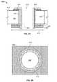
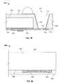
- FIGS. 2 a and 2 billustrate an example of a T-style contact.
- FIG. 2 ashows a schematic frontal 200 view and FIG. 2 b a cross-sectional view 250 of a single T-style contact of a semiconductor package.
- the dieis drawn upside down so the front face 201 / 251 is towards the bottom of the page and the rear face 202 / 252 towards the top of the page.
- a bond pad 203 / 253 on the front faceconnects to the wiring trace 204 / 254 on the edge of the die.
- the wiring tracecontinues to a land 205 / 255 on the rear face, where it joins to a solder sphere 206 / 256 .
- the shape of the T-style contact 257is evident in the cross-sectional view, while the sidewall angle 207 is indicated in the frontal view.
- the drawingis not to scale.
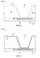
- FIG. 3is a cross-section view 300 of a typical TSV.
- the TSVis a hole (or blind via) extending through the thickness of the semiconductor that terminates on the underside of a bond pad 304 .
- the sides or wall of the through holeare coated with metal to form an electrically conductive pathway between the front and rear surfaces of the die.
- a deep reactive ion etching process known in the engineering community as the ‘Bosch process’may be used to form the TSV shown in FIG. 3 .
- the contact to the bond pad 304 shown in FIG. 3is often described as U-style. To complete the electrical circuit between the underside of the die bond pads and the conductive coating applied to the walls of TSVs requires a solid state bond between the two metals.
- FIG. 3shows the semiconductor die inverted with a front face 301 and a rear face 302 .
- a hole 310extends through the thickness of the die and the dielectric film 303 underneath the bond pad 304 to terminate on the bond pad 304 .
- a dielectric material 311 and a conductive coating 312line the walls of the hole. Both the dielectric material lining the through hole 310 and the conductive coating 312 extend on to an area of the rear face 302 of the die.
- Hole 310 extending through the siliconis parallel-sided and perpendicular to the die faces 301 and 302 .
- a microelectronic unitcan include a semiconductor element having a front surface, a microelectronic semiconductor device adjacent to the front surface, contacts at the front surface and a rear surface remote from the front surface.
- the semiconductor elementcan have through holes extending from the rear surface through the semiconductor element and through the contacts.
- a dielectric layercan line the through holes.
- a conductive layermay overlie the dielectric layer within the through holes. The conductive layer can conductively interconnect the contacts with unit contacts.
- a microelectronic unitcan include a semiconductor element having a front surface, a plurality of contacts at the front surface and a rear surface remote from the front surface.
- the rear surfacecan include at least one recess.
- a plurality of through holescan extend from the recess through the semiconductor element and through the contacts. Conductive vias within the through holes can interconnect the contacts with conductors within the at least one recess.
- a microelectronic unitcan include a plurality of semiconductor elements stacked and joined together.
- Each semiconductor elementcan have a front surface defining a horizontal plane, contacts at the front surface and a rear surface remote from the front surface.
- the semiconductor elementscan be stacked in a vertical direction transverse to the horizontal plane.
- a plurality of through holescan extend through at least one of the stacked semiconductor elements and through contacts of the at least one semiconductor element.
- the contacts of the plurality of stacked semiconductor elementscan be exposed within the through holes.
- a dielectric layercan line the through holes and a conductive layer can overlie the dielectric layer within the through holes.
- the conductive layercan be in conductive communication with unit contacts of the microelectronic unit.
- a microelectronic unitcan include a semiconductor element having a front surface, contacts at the front surface, a rear surface remote from the front surface, and edges extending between the front and rear surface.
- a dielectric elementcan extend outwardly from at least one of the edges of the semiconductor element.
- the dielectric elementcan have a front surface and a rear surface remote from the front surface and can include a plurality of conductive pads connected to the contacts.
- the dielectric elementcan also include a plurality of through holes extending between the front and rear surfaces and through the plurality of conductive pads.
- a plurality of unit contactscan be exposed at an exterior of the microelectronic unit. Conductive features can extend from the contacts within the through holes and can be in conductive communication with the unit contacts.
- a method of forming a unit contact exposed at a rear face of a microelectronic elementcan include forming a first through hole extending from a rear face of the microelectronic element towards an element contact at a front face of the microelectronic element.
- An insulative coatingcan be formed overlying at least a wall of the first hole.
- a second holecan be formed to extend through the element contact.
- the unit contact exposed at the rear facecan be formed including a conductive material which can overlie the wall of the first hole and can overlie a wall of the second hole and be conductively connected with the element contact.
- a method of forming a unit contact exposed at a rear face of a microelectronic elementcan include (a) forming a through hole extending from a rear face of the microelectronic element through an element contact at a front face of the microelectronic element.
- An insulative layercan be exposed at a wall of the hole.
- the microelectronic elementcan include forming the unit contact exposed at the rear face, including a conductive layer overlying the insulative layer and conductively connected with the element contact.
- FIG. 1is a perspective view of a semiconductor die having die bond pads on its periphery.
- FIG. 2 ais a front (elevational) view and FIG. 2 b is a sectional view illustrating a conventional chip-scale semiconductor package having a T-style contact.
- FIG. 3is a sectional view illustrating a semiconductor package having a through silicon via exposing an underside (inner surface) of a bond pad.
- FIG. 4 ais a sectional view illustrating a semiconductor package having a through silicon via, according to one embodiment of the invention.
- FIG. 4 bis a corresponding plan view further illustrating the semiconductor package shown in FIG. 4 a.
- FIG. 4 cis a sectional view illustrating a variation of the semiconductor package of FIG. 4 a.
- FIGS. 4 d - 4 hare sectional views illustrating stages in a process of forming a conductive via according to one embodiment of the invention.
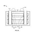
- FIG. 5 ais a sectional view illustrating a microelectronic unit including a plurality of vertically stacked semiconductor elements, according to one embodiment of the invention.
- FIG. 5 bis a sectional view illustrating a microelectronic unit according to a variation of the embodiment illustrated in FIG. 5 a.
- FIG. 6 ais a partial plan view illustrating a portion of a reconstituted wafer including a semiconductor element and a dielectric element adjacent to an edge of the semiconductor element, according to one embodiment of the invention.
- FIG. 6 bis a corresponding sectional view illustrating conductive traces extending between the semiconductor element and the dielectric element of the reconstituted wafer shown in FIG. 6 a , according to one embodiment of the invention.
- FIGS. 7 a - 7 bare sectional views of the reconstituted wafer shown in FIGS. 6 a - 6 b , further illustrating a through via extending through the dielectric element and a contact thereon.
- FIGS. 8 a - 8 fare sectional views illustrating stages in a process of forming a conductive via according to one embodiment of the invention.
- FIG. 9is a plan view illustrating a microelectronic unit in which conductive interconnects to multiple bond pads extend through a common opening.
- FIG. 10 ais a sectional view illustrating a portion of a wafer and openings in and between two adjacent semiconductor elements, e.g., die, according to one embodiment of the invention.
- FIG. 10 bis a corresponding plan view illustrating several adjacent die in the portion of the wafer shown in FIG. 10 a , according to one embodiment of the invention.
- a contact “exposed at” a surface of a dielectric elementmay be flush with such surface; recessed relative to such surface; or protruding from such surface, so long as the contact is accessible by a theoretical point moving towards the surface in a direction perpendicular to the surface.
- the through conductorsmay include elements such as solid metallic spheres, solder connections or other metallic elements.
- contactsmay be disposed at the same locations as the through conductors, or at different locations.
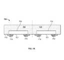
- FIG. 1is a perspective drawing or isometric drawing, not to scale, of a typical semiconductor die 100 .
- the die 100includes a the front face 101 , die edges 102 and bond pads 103 arrayed adjacent the die periphery. Not directly visible, but present by implication, are the rear face 104 of the die and the active circuitry 105 buried just below the surface of the front face 101 .
- T-style contactbetween a wiring trace on the edge of a die or the sidewall of a TSV and a bond pad on the front face of a die.
- This contactcan be used to complete an electrical pathway between the die bond pad and a BGA interface on the opposing face of the die.
- this structurealso affords the possibility of other interconnect configurations including TSVs fabricated, i.e., etched, starting from the front face of the die and double-sided contacts.
- Some benefits of various embodiments of the inventioninclude high interconnection density per unit area, simple fabrication processes and pathways through the die thickness offering low electrical resistance.
- FIGS. 4 a and 4 billustrate an example of a TSV that extends through a microelectronic element 400 e.g. a silicon die.
- FIG. 4 ais a cross-section view of a through silicon via TSV formed along a through hole 410 that extends completely through the entire thickness of a semiconductor die. This includes a semiconductor material region 401 of the die, the bond pad 403 , and the dielectric film 402 underneath the bond pad 403 .
- a dielectric material, such as an insulative coating, 411lines a wall 420 of a through hole, extending through the semiconductor region 401 .
- the thickness 416 of the semiconductor region of the diecan range from a few tens of microns to several hundred microns.
- Some semiconductor wafersfor example, have a thickness of 800 microns.
- a typical bond pad width 415 along the surface (front face) of the dieis 100 microns, which typically is the same or similar to the length of the bond pad along the front surface.
- the intersection between the bond pad 403 and the hole 410optionally is contained entirely within the area of the bond pad 403 .
- a conductorwhich may be in the form of a conductive coating 412 as shown in FIG. 4 a , contacts edges of the bond pad 403 within the through hole 410 and extends through the hole 410 to the rear face 404 .
- the conductive coating 412can contact an edge of the bond pad 403 exposed by the through hole 410 to form a T-style contact 405 .
- Both the dielectric material 411 lining wall 420 of the through hole 410 and the conductive coating 412 or other conductoroptionally extends onto an area of the rear face 404 of the die.
- TSVs having vertical sidewallsmay present difficulties in processing.
- Such TSVsmay have high aspect ratios, where the height of each TSV exceeds the diameter of the TSV, sometimes by a factor of two or more.
- high aspect ratio TSVscan make vapor deposition processes and electrodeposition processes (e.g., electrophoretic coating and various electroplating processes) more difficult to control.
- the hole 410can have a tapered shape such that the size of the hole increases with increasing distance from the front surface. In such case, the diameter of the hole increases with increasing distance from the front face of the die.
- Such shapeprovides for a radially symmetric T-style contact.
- Formation of a hollow hole through the die, that is parallel-sided and perpendicular to the die surfacesis readily accomplished by any machining process that is not material selective. Examples include, mechanical drilling, laser ablation, and certain wet etches and activated plasma chemistries. Of these, laser ablation may be relatively easy to instigate in volume manufacture owing to the combination of the speed of material removal, coupled with the benefits of soft tooling associated with this process.
- the machining process used to form the holepenetrates the thickness of the bond pad it exposes virgin metal of the bond pad. This means there is no need for scrupulous cleaning post-machining of the hole and prior to application of the conductive coating on a wall of the hole. This simplifies the processing.
- a hole 410can be etched in a semiconductor region 401 of the microelectronic element to expose a surface of a dielectric layer 402 between the element contact 403 and the semiconductor region.
- An insulative layer 411( FIG. 4 e ) can then be formed which extends along a wall 420 of the hole.
- the hole 410can be extended through the dielectric layer 402 and the element contact 403 . If the insulative layer 411 lines a bottom of the hole when formed, (such as depicted in FIG.
- the process of extending the holemay cause the hole to pass through a portion of the insulative layer 411 ( FIG. 4 f ).
- conductive material 412can then be deposited in contact with the element contact 403 and the insulative layer 411 of the hole, as illustrated in FIG. 4 a.
- a hole 410may be formed through the semiconductor region 401 , dielectric layer 402 and element contact 403 in a single step, as seen in FIG. 4 g .
- the holemay be formed using laser ablation or drilling.
- an insulative layer 411may be formed over just the semiconductor region 401 , as seen in FIG. 4 h .
- Such an insulative layermay be formed using electrophoretic deposition.
- conductive material 412can then be deposited in contact with the element contact 403 and the insulative layer 411 of the hole, as illustrated in FIG. 4 a .
- Such a conductive layermay be formed using chemical vapour deposition, sputtering or physical vapour deposition.
- the conductormay be in the form of a solid conductor which fills the hole, or may be in the form of a conductive coating but extend along only a portion of the wall.
- the dielectric layer lining the holeneed not extend onto the rear face of the die.
- TSVs of the type shown in FIGS. 4 a - 4 care compatible with stacks of die where bond pads on each layer of die are aligned when viewed in plan ( FIG. 5 a ).
- a TSV technology that is able to traverse multiple layers of diemakes it possible to connect all of these bond pads in parallel in a single process step.
- a resulting microelectronic unitincludes vertically aligned die 501 joined together in a stack, each die having T-style contacts conductively interconnecting the bond pads 502 of each die with unit contacts 504 , as illustrated in FIG. 5 a.
- FIG. 5 ashows the principal features of the structure by way of illustration and is not to scale.
- FIG. 5 ais a cross-section drawing through a stack of die 500 .
- the TSV 510extends completely through the dies 501 and bond pads 502 , so each connection to the bond pad is by a frusto-conical T-style contact.
- Two additional featuresare included in this figure by way of completeness. These are the encapsulant 503 that surrounds each die and holds the stack together and the BGA interface 504 on top of the die stack.
- FIG. 5 aillustrates TSVs having vertical and taperless walls
- alternative embodimentsmay not be exactly vertical and taperless, regardless of whether they pass through a single die or stack of die.
- the TSVsmay be both tapered and deviate from the vertical.
- the only restrictionis that the TSV must be smaller in diameter than the bond pads through which it passes, as illustrated in FIG. 4 b . This maximizes the length of the T-style contact.
- a TSV formed partially outside of a bond padrisks damaging circuitry on the die.
- the TSVsmay, or may not, be filled with dielectric or conductive material, depending on the electrical characteristics desired of the pathway and which will differ for high power and high frequency applications.
- the structurecan be fabricated by machining from either the front or the rear face of the die. Indeed, should other considerations dictate, it is also possible to machine the TSV from both sides with aligned TSVs meeting within the depth of the die. Following completion of the TSV, it is apparent that the die now has bond pads on the front face coupled to lands in an identical location on the rear face. From the point of view of making electrical connection to the die, it is now effectively a double-sided component so it can be mounted in either the face up or face down orientation.
- this new form of TSVcan be used to convey electrical signals from one side of the die to the other, without interacting with the circuitry on the die, provided the bond pad is a dummy feature with no connection to the die circuitry.
- the conductive element of the TSVhas to be electrically isolated from the semiconductor through which it passes, otherwise the electrical pathways would all be shorted to each other.
- This dielectric layerhas to be applied after the machining of the hole, but its application must not extend to the exposed metal of the bond pad that will be used to make the T-style contact.
- Oneis to create a dielectric layer by oxidation of the exposed semiconductor. This works if the semiconductor is silicon, since silica (silicon oxide) is an insulator. Chemistries exist that will oxidize silicon but leave the metal of the bond pad in a metallic state.
- FIG. 5 bshows a stacked microelectronic unit in which TSVs 520 extend through a first semiconductor die 511 and bond pads 522 of the first die, the TSVs exposing bond pads 524 at a front face of a second die 512 .
- a dielectric material 516can be exposed between opposing faces of the two die.
- a conductive layer 528conductively interconnects bond pads 522 of the first die, pads 524 of the second die 512 and unit contacts 544 of the unit.
- a plurality of first diecan be stacked and interconnected with the second die 512 by conductive layers within TSVs.
- FIG. 6 aillustrates a die built in a reconstituted wafer according to one embodiment of the invention.
- the silicon die 601is surrounded on at least four faces (five if the underside of the die is covered) by a dielectric material 602 .
- the bond pads 603 on the die 601are connected by a wiring trace 604 to new bond pads 605 on the dielectric material 602 .
- a partial sectional view along one wiring traceis given in FIG. 6 b 650 .
- the wiring trace 654is isolated from the semiconductor by a dielectric film 652 that is applied to the die as part of its manufacturing process.
- the dielectric film 652does not extend beyond the die periphery because the material used to construct the reconstituted wafer and which surrounds the die, is also dielectric in nature.
- each dieusually are surrounded by dielectric material, such as a solidified liquid polymer, for example, a dielectric overmold composition, as shown in FIG. 6 a .
- the dielectric materialmay also cover the rear face of each die.
- the dielectric material 602does not usually cover the front face of the die 601 but is flush with it.
- Part of the process of manufacturing the reconstituted wafersis to apply a patterned metal coating to the front face.
- the function of this wiring traceis to connect the die bond pads to similar pads outside of the die area. These new bond pads are formed of a conductive materials such as metal overlying the dielectric material.
- a conductive materialssuch as metal overlying the dielectric material.
- the through viaswill be formed which extend through the dielectric material 602 surrounding the die. Consequently, the through vias will not require an additional dielectric film to isolate the conductive coating on the via from the dielectric material through which it passes.
- a simpler, economical processis achieved particularly when through vias are formed en masse with respect to one or more reconstituted wafers or stack of reconstituted wafers. Reconstituted wafers can be used for both single die applications as well as die stacks.
- FIGS. 7 a and 7 billustrate cross-sectional views through a die formed on a reconstituted wafer 700 according to one embodiment of the invention.
- Reconstituted wafersare discussed in greater detail in PCT App. US08/09207, filed Jul. 25, 2008, entitled, “RECONSTITUTED WAFER STACK PACKAGING WITH AFTER-APPLIED PAD EXTENSIONS,” which claims the benefit of U.S. Provisional App. No. 60/962,200, filed Jul. 27, 2007, entitled, “RECONSTITUTED WAFER STACK PACKAGING WITH AFTER-APPLIED PAD EXTENSIONS,” the disclosures of which are both incorporated by reference herein. Further, additional detail is provided in U.S. patent application Ser. No.
- the die bond pad 702Overlying the die face 701 is the die bond pad 702 and its associated dielectric coating 703 on the die.
- the dieis surrounded on its sides and rear face 704 by a dielectric fill 705 of the reconstituted wafer.
- the through via 710( FIG. 7 b ) is stepped, and has a first through hole 711 and a second through hole 713 .
- the first through hole 711has a tapered profile to aid deposition of the conductive coating 712 on a wall of the first through hole 711 .
- a second bond pad 714is formed on a lower surface 715 of the dielectric fill layer 705 , the second bond pad 714 being conductively connected to the die bond pad 702 .
- the conductive coating 712extends along walls of the second through hole 713 in the second bond pad 714 . In this way, a via extension in the second through hole 713 makes conductive contact with the second bond pad 714 . After application of the conductive coating to this region, the result is a frusto-conical T-style contact between the second bond pad 714 and the via extension 713 .
- Machining of TSVs through semiconductor die and machining of through vias penetrating dielectric layersmay be accomplished by a variety of processes.
- a combination of processesmay offer manufacturing advantages so that, for example, plasma etching is used to machine through the thickness of the silicon to produce a tapered via and the hole is extended through the bond pad by laser ablation.
- the resulting structurehas the benefit that the taper angle through the silicon aids application of coatings to the wall of the TSV, while the laser ablation can be used to create a small diameter hole through the bond pad.
- the interconnectcan thus have a stepped diameter structure, as illustrated for a die built from a reconstituted wafer in FIG. 7 .
- a TSV having a taper anglecan generally be produced with a lower ohmic resistance than a purely vertical via, owing to the combination of a larger surface area and increased thickness of metal applied for a given deposition time compared with a parallel-sided via.
- FIGS. 8 a thru 8 fillustrate a process for forming a TSV according to one embodiment of the invention.
- FIG. 8 fillustrates a cross-sectional view of a TSV extending through semiconductor die according to one embodiment of the invention.
- FIG. 8 aillustrates a partial cross-section through a semiconductor die 801 .
- the front face 802 of the dieis opposite, i.e., remote from its rear face 803 and includes a bond pad 804 that is isolated from the semiconductor die 801 by a dielectric film 805 .
- the dieis shown with protective dielectric film 806 covering all of its features.
- This film 806is representative of structures which can be present in certain types of die packages such as, any variety of compliant layers, die attach films, die stacking adhesives, or combination thereof.
- FIG. 8 billustrates forming a first hole extending from the rear surface 802 of the die 801 to the active surface of the die.
- the first hole 807has a bottom surface positioned above the dielectric film 805 .
- a plasma etch processmay be used to form a first hole 807 through the thickness of the silicon in accordance with one embodiment. Because the plasma process is material selective, the first hole 807 stops at the dielectric film 805 on which the bond pad 804 sits.
- the first hole 807can have a tapered profile, having the largest area at the rear face 803 of the die. Such a tapered profile may aid subsequent coating of its surfaces.
- first hole 807may be formed by wet etching or mechanical milling.
- FIG. 8 cillustrates forming an insulative coating 808 over the rear surface 803 of the die according to one embodiment.
- the insulative coating 808forms an insulative layer within the first hole 807 .
- a dielectric filme.g., an electrocoat material
- electrocoat materialmay be applied to the rear face of the die, such as by electrophoretic deposition. By the nature of the electrocoat material this will be conformal and therefore coat the walls of the first hole 807 as well as the dielectric film 805 underneath the bond pad 804 .
- other dielectric filmssuch as solder mask or photo-resist may be used.
- FIG. 8 dillustrates forming a second hole 809 extending through the insulative layer 808 , dielectric film 805 and bond pad 804 according to one embodiment. As seen in FIG. 8 d , the diameter of the second hole 809 is contained within the bond pad 804 .
- laser ablationmay be used to form the second hole 809 through the thickness of insulative material 808 , the dielectric film 805 and the bond pad 804 . If there is nothing over the bond pad, then the result is a through hole. However, in this instance, the front face of the die is covered by a dielectric material 816 . In that case, it is possible for the laser ablated second hole to pass through the dielectric film and the bond pad and terminate in the die covering 816 , effectively forming a closed hole or a blind hole.
- the die covering 816may be formed of solder mask. Furthermore, the die covering 816 may be used to form the side walls of a cavity between the die and a glass layer (not shown).
- a stepped through hole 815 , through die 801 and bond pad 804is formed by the first hole 807 and the second hole 809 and extends from the rear surface 803 of the die thru the bond pad 804 .
- FIG. 8 eillustrates forming a conductive layer 810 that can include metal, according to one embodiment.
- the conductive layer 810is then applied to the inside surfaces of the through hole 815 created by the first and second holes. Because the stepped through hole 815 passes through the bond pad 804 , it will form a radially symmetric T-style contact 811 .
- the TSVcan be formed by coating the holes with metal or by filling the holes with metal.
- One process that can be used for applying a metal coatingis a vapor phase deposition, examples of which include evaporation and sputtering. These processes will also deposit metal on the rear face of the die. By patterning this film it is possible to create a BGA interface 812 where each site for a solder ball is connected to a via and the die bond pad as seen in FIG. 8 f .
- the thickness of the applied metalmay be substantially increased by about an order of magnitude by additional processing such as electroplating.
- the viacan be filled completely with an electrically conductive material.
- a layer 813 of dielectric materialcan be deposited overlying the conductive layer 810 in the holes as shown in FIG. 8 f .
- Exposed metal of the wiring tracescan be covered by an organic protective dielectric coating.
- a common materialis solder mask. The completed structure can then appear as shown in FIG. 8 f.
- FIGS. 8 a thru 8 fillustrate the formation of vias to provide electrical contact between a bond pad formed on a die and a BGA interface according to an embodiment of the present invention.
- the holesextend from the rear surface of the diethrough the bond pad. Furthermore, the diameter of the second hole does not extend beyond the perimeter of the bond pads.
- the first and second holesneed not be circular.
- the first holecan be greatly elongated to form a notch or trench that spans several bond pads.
- Second holesthen pass through bond pads at the base of the notch or trench on a singular basis. This embodiment requires the metal coating on the sidewall of the notch or trench to be patterned unless it is desired that a row of bond pads are connected in parallel. This is sometimes the case for bond pads that supply electrical power to a semiconductor.
- Typical dimensions for both die bond pads or bond pads on dielectric regions of reconstituted wafersare in the region of 100 ⁇ m on a side.
- a typical TSVwill have a diameter of about 50 ⁇ m if parallel-sided, and about 50 ⁇ m at the base and about 80 ⁇ m at the opening if tapered.
- the extension of the TSV through the bond padwill be slightly smaller at around 20 ⁇ m diameter.
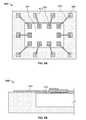
- FIG. 9provides a plan view of a TSV located over four bond pads according to one embodiment of the invention.
- the TSVhas patterned metal on the side walls, permitting a separate pathway to be made to each bond pad.
- Four bond pads 901 , 902 , 903 and 904are exposed at the front face of the die.
- a tapered via 905passes through a portion of all four bond pads.
- the metal on the TSVis patterned 906 , 907 , 908 and 909 to provide individual arcs of T-style contacts to the bond pads.
- Formation of the TSVsis preferably done at the wafer level since it allows all of the structures to be fabricated in parallel, so the process costs are shared among all of the yielding parts.
- the wafermust be singulated to free individual die. This may be accomplished by mechanical sawing. Alternatively, it can be organised so that when the semiconductor is being machined to form the hole of the TSV, material is also removed from the dicing street, as shown in FIG. 10 a . Singulation then involves removing or cutting through any material present in the dicing street on the front of the wafer, or simply cleaving it. All of these processes are quicker to perform than dicing through the full thickness of the semiconductor plus those layers.
- the TSVs used for electrical connectionare preferably circular, it will be apparent that to separate the die on the wafer, the TSVs fabricated in the streets can be in the form of a slot in the street (dicing lane) between each die, as illustrated in FIG. 10 b .
- the diecan remain connected by small ligaments of semiconducting material at each corner as this retains electrical continuity over the entire rear surface of the wafer from a single point of electrical contact. This attribute can be helpful for the next process step which is the application of the electrocoat dielectric film.
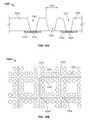
- FIGS. 10 a and 10 bindicate how a process used to form a TSV can be used to simultaneously remove the semiconductor material from the dicing street (dicing lane), aiding subsequent singulation of die from a wafer according to one embodiment of the invention.
- Shown in FIG. 10 ais a dicing street 1001 between two adjacent die 1010 and 1020 on a wafer. Each die has a TSV 1011 / 1021 hole formed through the silicon to the dielectric film 1012 / 1022 underneath the bond pad 1013 / 1023 .
- another TSV 1002has been fabricated in the dicing street.
- FIG. 10 bis a plan view 1050 of the rear face of several adjacent die on a wafer. Circular TSVs 1051 have been formed to contact each bond pad, while slot-shaped TSVs 1052 have been machined in the dicing streets at the same time as part of the singulation process. Ligaments of semiconductor 1054 remain at each intersection of four die corners to provide the electrical continuity of the wafer face for the subsequent electrocoat process.
Landscapes
- Engineering & Computer Science (AREA)
- Microelectronics & Electronic Packaging (AREA)
- Power Engineering (AREA)
- Computer Hardware Design (AREA)
- Physics & Mathematics (AREA)
- Condensed Matter Physics & Semiconductors (AREA)
- General Physics & Mathematics (AREA)
- Manufacturing & Machinery (AREA)
- Internal Circuitry In Semiconductor Integrated Circuit Devices (AREA)
Abstract
Description
Claims (32)
Priority Applications (2)
| Application Number | Priority Date | Filing Date | Title |
|---|---|---|---|
| US12/221,204US8193615B2 (en) | 2007-07-31 | 2008-07-31 | Semiconductor packaging process using through silicon vias |
| US13/488,930US8735287B2 (en) | 2007-07-31 | 2012-06-05 | Semiconductor packaging process using through silicon vias |
Applications Claiming Priority (2)
| Application Number | Priority Date | Filing Date | Title |
|---|---|---|---|
| US96275207P | 2007-07-31 | 2007-07-31 | |
| US12/221,204US8193615B2 (en) | 2007-07-31 | 2008-07-31 | Semiconductor packaging process using through silicon vias |
Related Child Applications (1)
| Application Number | Title | Priority Date | Filing Date |
|---|---|---|---|
| US13/488,930DivisionUS8735287B2 (en) | 2007-07-31 | 2012-06-05 | Semiconductor packaging process using through silicon vias |
Publications (2)
| Publication Number | Publication Date |
|---|---|
| US20090065907A1 US20090065907A1 (en) | 2009-03-12 |
| US8193615B2true US8193615B2 (en) | 2012-06-05 |
Family
ID=40305147
Family Applications (2)
| Application Number | Title | Priority Date | Filing Date |
|---|---|---|---|
| US12/221,204ActiveUS8193615B2 (en) | 2007-07-31 | 2008-07-31 | Semiconductor packaging process using through silicon vias |
| US13/488,930ActiveUS8735287B2 (en) | 2007-07-31 | 2012-06-05 | Semiconductor packaging process using through silicon vias |
Family Applications After (1)
| Application Number | Title | Priority Date | Filing Date |
|---|---|---|---|
| US13/488,930ActiveUS8735287B2 (en) | 2007-07-31 | 2012-06-05 | Semiconductor packaging process using through silicon vias |
Country Status (6)
| Country | Link |
|---|---|
| US (2) | US8193615B2 (en) |
| EP (1) | EP2183770B1 (en) |
| JP (2) | JP2010535427A (en) |
| KR (2) | KR101538648B1 (en) |
| CN (2) | CN101802990B (en) |
| WO (1) | WO2009017835A2 (en) |
Cited By (21)
| Publication number | Priority date | Publication date | Assignee | Title |
|---|---|---|---|---|
| US20100230795A1 (en)* | 2009-03-13 | 2010-09-16 | Tessera Technologies Hungary Kft. | Stacked microelectronic assemblies having vias extending through bond pads |
| US20120241976A1 (en)* | 2007-07-31 | 2012-09-27 | DigitalOptics Corporation Europe Limited | Semiconductor packaging process using through silicon vias |
| US8587126B2 (en) | 2010-12-02 | 2013-11-19 | Tessera, Inc. | Stacked microelectronic assembly with TSVs formed in stages with plural active chips |
| US8610259B2 (en) | 2010-09-17 | 2013-12-17 | Tessera, Inc. | Multi-function and shielded 3D interconnects |
| US8637968B2 (en) | 2010-12-02 | 2014-01-28 | Tessera, Inc. | Stacked microelectronic assembly having interposer connecting active chips |
| US8736066B2 (en) | 2010-12-02 | 2014-05-27 | Tessera, Inc. | Stacked microelectronic assemby with TSVS formed in stages and carrier above chip |
| US8735205B2 (en) | 2007-03-05 | 2014-05-27 | Invensas Corporation | Chips having rear contacts connected by through vias to front contacts |
| US8791575B2 (en) | 2010-07-23 | 2014-07-29 | Tessera, Inc. | Microelectronic elements having metallic pads overlying vias |
| US8796135B2 (en) | 2010-07-23 | 2014-08-05 | Tessera, Inc. | Microelectronic elements with rear contacts connected with via first or via middle structures |
| US8796828B2 (en) | 2010-12-08 | 2014-08-05 | Tessera, Inc. | Compliant interconnects in wafers |
| US8847380B2 (en) | 2010-09-17 | 2014-09-30 | Tessera, Inc. | Staged via formation from both sides of chip |
| US8865544B2 (en) | 2012-07-11 | 2014-10-21 | Micron Technology, Inc. | Methods of forming capacitors |
| US9048234B2 (en) | 2006-10-10 | 2015-06-02 | Tessera, Inc. | Off-chip vias in stacked chips |
| US9070678B2 (en) | 2006-11-22 | 2015-06-30 | Tessera, Inc. | Packaged semiconductor chips with array |
| US9318385B2 (en) | 2011-06-24 | 2016-04-19 | Tessera, Inc. | Systems and methods for producing flat surfaces in interconnect structures |
| US9378967B2 (en) | 2006-10-10 | 2016-06-28 | Tessera, Inc. | Method of making a stacked microelectronic package |
| US9640437B2 (en) | 2010-07-23 | 2017-05-02 | Tessera, Inc. | Methods of forming semiconductor elements using micro-abrasive particle stream |
| US9646899B2 (en) | 2012-09-13 | 2017-05-09 | Micron Technology, Inc. | Interconnect assemblies with probed bond pads |
| US10923397B2 (en) | 2018-11-29 | 2021-02-16 | Globalfoundries Inc. | Through-substrate via structures in semiconductor devices |
| US10957626B2 (en) | 2017-12-19 | 2021-03-23 | Thermo Electron Scientific Instruments Llc | Sensor device with carbon nanotube sensor positioned on first and second substrates |
| US12381168B2 (en) | 2015-08-25 | 2025-08-05 | Adeia Semiconductor Bonding Technologies Inc. | Conductive barrier direct hybrid bonding |
Families Citing this family (46)
| Publication number | Priority date | Publication date | Assignee | Title |
|---|---|---|---|---|
| EP1517166B1 (en) | 2003-09-15 | 2015-10-21 | Nuvotronics, LLC | Device package and methods for the fabrication and testing thereof |
| US7829438B2 (en) | 2006-10-10 | 2010-11-09 | Tessera, Inc. | Edge connect wafer level stacking |
| US7791199B2 (en) | 2006-11-22 | 2010-09-07 | Tessera, Inc. | Packaged semiconductor chips |
| US7952195B2 (en) | 2006-12-28 | 2011-05-31 | Tessera, Inc. | Stacked packages with bridging traces |
| JP4919984B2 (en)* | 2007-02-25 | 2012-04-18 | サムスン エレクトロニクス カンパニー リミテッド | Electronic device package and method for forming the same |
| JP5572089B2 (en) | 2007-07-27 | 2014-08-13 | テッセラ,インコーポレイテッド | Reconfigured wafer stack packaging with pad extension after application |
| US8551815B2 (en) | 2007-08-03 | 2013-10-08 | Tessera, Inc. | Stack packages using reconstituted wafers |
| US8043895B2 (en) | 2007-08-09 | 2011-10-25 | Tessera, Inc. | Method of fabricating stacked assembly including plurality of stacked microelectronic elements |
| JP2009181981A (en)* | 2008-01-29 | 2009-08-13 | Renesas Technology Corp | Manufacturing process of semiconductor device, and the semiconductor device |
| US20100053407A1 (en)* | 2008-02-26 | 2010-03-04 | Tessera, Inc. | Wafer level compliant packages for rear-face illuminated solid state image sensors |
| US20090212381A1 (en)* | 2008-02-26 | 2009-08-27 | Tessera, Inc. | Wafer level packages for rear-face illuminated solid state image sensors |
| JP5639052B2 (en) | 2008-06-16 | 2014-12-10 | テッセラ,インコーポレイテッド | Edge stacking at wafer level |
| SG158823A1 (en)* | 2008-07-18 | 2010-02-26 | United Test & Assembly Ct Ltd | Packaging structural member |
| US8552563B2 (en)* | 2009-04-07 | 2013-10-08 | Taiwan Semiconductor Manufacturing Company, Ltd. | Three-dimensional semiconductor architecture |
| WO2011044393A1 (en) | 2009-10-07 | 2011-04-14 | Tessera North America, Inc. | Wafer-scale emitter package including thermal vias |
| US8455356B2 (en) | 2010-01-21 | 2013-06-04 | International Business Machines Corporation | Integrated void fill for through silicon via |
| CN102376629B (en)* | 2010-08-17 | 2013-07-03 | 中国科学院上海微系统与信息技术研究所 | Method for realizing through silicon via interconnection by means of suspension photoresist |
| US8686565B2 (en) | 2010-09-16 | 2014-04-01 | Tessera, Inc. | Stacked chip assembly having vertical vias |
| US8685793B2 (en) | 2010-09-16 | 2014-04-01 | Tessera, Inc. | Chip assembly having via interconnects joined by plating |
| KR101059490B1 (en) | 2010-11-15 | 2011-08-25 | 테세라 리써치 엘엘씨 | Conductive pads constructed by embedded traces |
| US9171964B2 (en) | 2010-11-23 | 2015-10-27 | Honeywell International Inc. | Systems and methods for a three-layer chip-scale MEMS device |
| US8748206B2 (en) | 2010-11-23 | 2014-06-10 | Honeywell International Inc. | Systems and methods for a four-layer chip-scale MEMS device |
| CN102479765B (en)* | 2010-11-24 | 2016-08-24 | 日月光半导体制造股份有限公司 | Package structure with semiconductor components |
| US8975751B2 (en)* | 2011-04-22 | 2015-03-10 | Tessera, Inc. | Vias in porous substrates |
| US8987140B2 (en) | 2011-04-25 | 2015-03-24 | Applied Materials, Inc. | Methods for etching through-silicon vias with tunable profile angles |
| TWI489605B (en)* | 2011-05-13 | 2015-06-21 | Xintec Inc | Chip package and method of forming same |
| JP5598420B2 (en)* | 2011-05-24 | 2014-10-01 | 株式会社デンソー | Manufacturing method of electronic device |
| US8692118B2 (en) | 2011-06-24 | 2014-04-08 | Tessera, Inc. | Reliable wire structure and method |
| US9125333B2 (en) | 2011-07-15 | 2015-09-01 | Tessera, Inc. | Electrical barrier layers |
| CN102509718B (en)* | 2011-12-15 | 2014-02-12 | 中国科学院上海微系统与信息技术研究所 | GaAs CCD Graphic Sensor Wafer Level Chip Scale Packaging Technology |
| US8928114B2 (en)* | 2012-01-17 | 2015-01-06 | Taiwan Semiconductor Manufacturing Company, Ltd. | Through-assembly via modules and methods for forming the same |
| US9881894B2 (en) | 2012-03-08 | 2018-01-30 | STATS ChipPAC Pte. Ltd. | Thin 3D fan-out embedded wafer level package (EWLB) for application processor and memory integration |
| US9343497B2 (en)* | 2012-09-20 | 2016-05-17 | Semiconductor Components Industries, Llc | Imagers with stacked integrated circuit dies |
| US9312226B2 (en)* | 2012-12-14 | 2016-04-12 | Infineon Technologies Ag | Semiconductor device having an identification mark |
| US9070741B2 (en) | 2012-12-17 | 2015-06-30 | Infineon Technologies Austria Ag | Method of manufacturing a semiconductor device and a semiconductor workpiece |
| US9070667B2 (en)* | 2013-02-27 | 2015-06-30 | Taiwan Semiconductor Manufacturing Company, Ltd. | Peripheral electrical connection of package on package |
| JP6337419B2 (en)* | 2013-04-18 | 2018-06-06 | 大日本印刷株式会社 | Method for forming resist pattern and laminate structure |
| US9735134B2 (en)* | 2014-03-12 | 2017-08-15 | Taiwan Semiconductor Manufacturing Company, Ltd. | Packages with through-vias having tapered ends |
| JP6436738B2 (en)* | 2014-11-19 | 2018-12-12 | キヤノン株式会社 | Printed wiring board, semiconductor device and printed circuit board |
| US10773049B2 (en) | 2016-06-21 | 2020-09-15 | Ventec Life Systems, Inc. | Cough-assist systems with humidifier bypass |
| US10319654B1 (en) | 2017-12-01 | 2019-06-11 | Cubic Corporation | Integrated chip scale packages |
| US11171117B2 (en)* | 2018-06-12 | 2021-11-09 | Invensas Bonding Technologies, Inc. | Interlayer connection of stacked microelectronic components |
| WO2020108603A1 (en)* | 2018-11-30 | 2020-06-04 | Changxin Memory Technologies, Inc. | Method for fabricating semiconductor interconnect structure and semiconductor structure thereof |
| EP3671823A1 (en)* | 2018-12-21 | 2020-06-24 | ams AG | Semiconductor device with through-substrate via and method of manufacturing a semiconductor device with through-substrate via |
| CN115602639A (en)* | 2021-06-28 | 2023-01-13 | 合肥本源量子计算科技有限责任公司(Cn) | Quantum device, preparation method thereof and electronic device |
| CN117153780B (en)* | 2023-10-26 | 2024-01-30 | 甬矽电子(宁波)股份有限公司 | Method for producing a through-silicon-via structure and through-silicon-via structure |
Citations (85)
| Publication number | Priority date | Publication date | Assignee | Title |
|---|---|---|---|---|
| JPS60160645A (en) | 1984-02-01 | 1985-08-22 | Hitachi Ltd | Laminated semiconductor integrated circuit device |
| US4765864A (en) | 1987-07-15 | 1988-08-23 | Sri International | Etching method for producing an electrochemical cell in a crystalline substrate |
| US5481133A (en) | 1994-03-21 | 1996-01-02 | United Microelectronics Corporation | Three-dimensional multichip package |
| EP0926723A1 (en) | 1997-11-26 | 1999-06-30 | STMicroelectronics S.r.l. | Process for forming front-back through contacts in micro-integrated electronic devices |
| US6013948A (en) | 1995-11-27 | 2000-01-11 | Micron Technology, Inc. | Stackable chip scale semiconductor package with mating contacts on opposed surfaces |
| US6022758A (en) | 1994-07-10 | 2000-02-08 | Shellcase Ltd. | Process for manufacturing solder leads on a semiconductor device package |
| US6031274A (en) | 1996-10-11 | 2000-02-29 | Hamamatsu Photonics K.K. | Back irradiation type light-receiving device and method of making the same |
| US6103552A (en) | 1998-08-10 | 2000-08-15 | Lin; Mou-Shiung | Wafer scale packaging scheme |
| US6261865B1 (en) | 1998-10-06 | 2001-07-17 | Micron Technology, Inc. | Multi chip semiconductor package and method of construction |
| JP2001217386A (en) | 2000-02-03 | 2001-08-10 | Seiko Epson Corp | Semiconductor device, method of manufacturing the same, and electronic device |
| US6277669B1 (en) | 1999-09-15 | 2001-08-21 | Industrial Technology Research Institute | Wafer level packaging method and packages formed |
| US20010048591A1 (en) | 1997-11-25 | 2001-12-06 | Joseph Fjelstad | Microelectronics component with rigid interposer |
| US20020109236A1 (en) | 2001-02-09 | 2002-08-15 | Samsung Electronics Co., Ltd. | Three-dimensional multi-chip package having chip selection pads and manufacturing method thereof |
| US6472247B1 (en) | 2000-06-26 | 2002-10-29 | Ricoh Company, Ltd. | Solid-state imaging device and method of production of the same |
| US6492201B1 (en) | 1998-07-10 | 2002-12-10 | Tessera, Inc. | Forming microelectronic connection components by electrophoretic deposition |
| US6498387B1 (en) | 2000-02-15 | 2002-12-24 | Wen-Ken Yang | Wafer level package and the process of the same |
| US20030059976A1 (en) | 2001-09-24 | 2003-03-27 | Nathan Richard J. | Integrated package and methods for making same |
| US6608377B2 (en) | 2001-01-30 | 2003-08-19 | Samsung Electronics Co., Ltd. | Wafer level package including ground metal layer |
| US20040016942A1 (en) | 2002-04-24 | 2004-01-29 | Seiko Epson Corporation | Semiconductor device and a method of manufacturing the same, a circuit board and an electronic apparatus |
| US6693358B2 (en) | 2000-10-23 | 2004-02-17 | Matsushita Electric Industrial Co., Ltd. | Semiconductor chip, wiring board and manufacturing process thereof as well as semiconductor device |
| US20040043607A1 (en) | 2002-08-29 | 2004-03-04 | Farnworth Warren M. | Methods for creating electrophoretically insulated vias in semiconductive substrates and resulting structures |
| US6727576B2 (en) | 2001-10-31 | 2004-04-27 | Infineon Technologies Ag | Transfer wafer level packaging |
| US6737300B2 (en) | 2001-01-24 | 2004-05-18 | Advanced Semiconductor Engineering, Inc. | Chip scale package and manufacturing method |
| US6743660B2 (en) | 2002-01-12 | 2004-06-01 | Taiwan Semiconductor Manufacturing Co., Ltd | Method of making a wafer level chip scale package |
| US20040104454A1 (en) | 2002-10-10 | 2004-06-03 | Rohm Co., Ltd. | Semiconductor device and method of producing the same |
| US20040155354A1 (en) | 2000-06-02 | 2004-08-12 | Seiko Epson Corporation | Semiconductor device, method of fabricating the same, stack-type semiconductor device, circuit board and electronic instrument |
| US20040178495A1 (en) | 2003-03-14 | 2004-09-16 | Yean Tay Wuu | Microelectronic devices and methods for packaging microelectronic devices |
| US20040188819A1 (en) | 2003-03-31 | 2004-09-30 | Farnworth Warren M. | Wafer level methods for fabricating multi-dice chip scale semiconductor components |
| US20040188822A1 (en)* | 2003-01-15 | 2004-09-30 | Kazumi Hara | Semiconductor chip, semiconductor wafer, semiconductor device and method of manufacturing the same, circuit board, and electronic instrument |
| US6812549B2 (en)* | 2001-03-07 | 2004-11-02 | Seiko Epson Corporation | Wiring board and fabricating method thereof, semiconductor device and fabricating method thereof, circuit board and electronic instrument |
| US20040217483A1 (en) | 2003-04-30 | 2004-11-04 | Infineon Technologies Ag | Semiconductor device and method for fabricating the semiconductor device |
| US20040222508A1 (en) | 2003-03-18 | 2004-11-11 | Akiyoshi Aoyagi | Semiconductor device, electronic device, electronic apparatus, method of manufacturing semiconductor device, and method of manufacturing electronic device |
| EP1482553A2 (en) | 2003-05-26 | 2004-12-01 | Sanyo Electric Co., Ltd. | Semiconductor device and manufacturing method thereof |
| US6828175B2 (en) | 2002-08-29 | 2004-12-07 | Micron Technology, Inc. | Semiconductor component with backside contacts and method of fabrication |
| US20040251525A1 (en) | 2003-06-16 | 2004-12-16 | Shellcase Ltd. | Methods and apparatus for packaging integrated circuit devices |
| WO2004114397A1 (en) | 2003-06-20 | 2004-12-29 | Koninklijke Philips Electronics N.V. | Electronic device, assembly and methods of manufacturing an electronic device |
| US20050012225A1 (en) | 2002-11-15 | 2005-01-20 | Choi Seung-Yong | Wafer-level chip scale package and method for fabricating and using the same |
| US20050046002A1 (en) | 2003-08-26 | 2005-03-03 | Kang-Wook Lee | Chip stack package and manufacturing method thereof |
| US6864172B2 (en) | 2002-06-18 | 2005-03-08 | Sanyo Electric Co., Ltd. | Manufacturing method of semiconductor device |
| US6867123B2 (en) | 2001-02-08 | 2005-03-15 | Renesas Technology Corp. | Semiconductor integrated circuit device and its manufacturing method |
| US20050056903A1 (en) | 2003-08-28 | 2005-03-17 | Satoshi Yamamoto | Semiconductor package and method of manufacturing same |
| EP1519410A1 (en) | 2003-09-25 | 2005-03-30 | Interuniversitair Microelektronica Centrum vzw ( IMEC) | Method for producing electrical through hole interconnects and devices made thereof |
| JP2005093486A (en) | 2003-09-12 | 2005-04-07 | Seiko Epson Corp | Semiconductor device manufacturing method and semiconductor device |
| US20050156330A1 (en) | 2004-01-21 | 2005-07-21 | Harris James M. | Through-wafer contact to bonding pad |
| US20050260794A1 (en) | 2002-09-03 | 2005-11-24 | Industrial Technology Research Institute | Method for fabrication of wafer level package incorporating dual compliant layers |
| US20050282374A1 (en) | 2004-06-22 | 2005-12-22 | Samsung Electronics Co., Ltd. | Method of forming a thin wafer stack for a wafer level package |
| US20050287783A1 (en) | 2004-06-29 | 2005-12-29 | Kirby Kyle K | Microelectronic devices and methods for forming interconnects in microelectronic devices |
| US6982475B1 (en) | 1998-03-20 | 2006-01-03 | Mcsp, Llc | Hermetic wafer scale integrated circuit structure |
| EP1619722A1 (en) | 2003-04-16 | 2006-01-25 | Hamamatsu Photonics K. K. | Method for manufacturing backside-illuminated optical sensor |
| US20060017161A1 (en) | 2004-07-22 | 2006-01-26 | Jae-Sik Chung | Semiconductor package having protective layer for re-routing lines and method of manufacturing the same |
| US20060046348A1 (en) | 2004-09-01 | 2006-03-02 | Kang Byoung Y | Semiconductor chip packages and methods for fabricating the same |
| US20060046471A1 (en) | 2004-08-27 | 2006-03-02 | Kirby Kyle K | Methods for forming vias of varying lateral dimensions and semiconductor components and assemblies including same |
| US20060043598A1 (en) | 2004-08-31 | 2006-03-02 | Kirby Kyle K | Methods of manufacture of a via structure comprising a plurality of conductive elements, semiconductor die, multichip module, and system including same |
| US20060068580A1 (en) | 2004-09-28 | 2006-03-30 | Sharp Kabushiki Kaisha | Semiconductor device and fabrication method thereof |
| US20060079019A1 (en) | 2004-10-08 | 2006-04-13 | Easetech Korea Co., Ltd. | Method for manufacturing wafer level chip scale package using redistribution substrate |
| EP1653510A2 (en) | 2004-10-28 | 2006-05-03 | Sanyo Electric Co., Ltd. | Semiconductor device and manufacturing method of the same |
| US20060094231A1 (en) | 2004-10-28 | 2006-05-04 | Lane Ralph L | Method of creating a tapered via using a receding mask and resulting structure |
| US20060115932A1 (en) | 1997-12-18 | 2006-06-01 | Farnworth Warren M | Method for fabricating semiconductor components with conductive vias |
| EP1686627A1 (en) | 2005-01-28 | 2006-08-02 | Samsung Electro-Mechanics Co., Ltd. | Semiconductor package and method of manufacturing the same |
| US20060175697A1 (en) | 2005-02-02 | 2006-08-10 | Tetsuya Kurosawa | Semiconductor device having semiconductor chips stacked and mounted thereon and manufacturing method thereof |
| US7091062B2 (en) | 2003-10-15 | 2006-08-15 | Infineon Technologies Ag | Wafer level packages for chips with sawn edge protection |
| US20060264029A1 (en) | 2005-05-23 | 2006-11-23 | Intel Corporation | Low inductance via structures |
| US20060292866A1 (en) | 2005-06-23 | 2006-12-28 | Borwick Robert L | Low temperature method for fabricating high-aspect ratio vias and devices fabricated by said method |
| JP2007053149A (en) | 2005-08-16 | 2007-03-01 | Renesas Technology Corp | Semiconductor wafer and its manufacturing method |
| JP2007157844A (en) | 2005-12-01 | 2007-06-21 | Sharp Corp | Semiconductor device and manufacturing method of semiconductor device |
| US7271033B2 (en) | 2001-12-31 | 2007-09-18 | Megica Corporation | Method for fabricating chip package |
| US20070269931A1 (en)* | 2006-05-22 | 2007-11-22 | Samsung Electronics Co., Ltd. | Wafer level package and method of fabricating the same |
| US20080020898A1 (en) | 2005-08-29 | 2008-01-24 | Johnson Health Tech Co., Ltd. | Rapid circuit training machine with dual resistance |
| US20080116544A1 (en) | 2006-11-22 | 2008-05-22 | Tessera, Inc. | Packaged semiconductor chips with array |
| US20080164574A1 (en) | 2006-12-06 | 2008-07-10 | Sergey Savastiouk | Integrated circuits with conductive features in through holes passing through other conductive features and through a semiconductor substrate |
| US7413929B2 (en) | 2001-12-31 | 2008-08-19 | Megica Corporation | Integrated chip package structure using organic substrate and method of manufacturing the same |
| US20080246136A1 (en) | 2007-03-05 | 2008-10-09 | Tessera, Inc. | Chips having rear contacts connected by through vias to front contacts |
| US20080284041A1 (en) | 2007-05-18 | 2008-11-20 | Samsung Electronics Co., Ltd. | Semiconductor package with through silicon via and related method of fabrication |
| US20090014843A1 (en) | 2007-06-06 | 2009-01-15 | Kawashita Michihiro | Manufacturing process and structure of through silicon via |
| US20090032951A1 (en) | 2007-08-02 | 2009-02-05 | International Business Machines Corporation | Small Area, Robust Silicon Via Structure and Process |
| US20090032966A1 (en) | 2007-08-01 | 2009-02-05 | Jong Ho Lee | Method of fabricating a 3-D device and device made thereby |
| US20090039491A1 (en) | 2007-08-10 | 2009-02-12 | Samsung Electronics Co., Ltd. | Semiconductor package having buried post in encapsulant and method of manufacturing the same |
| US20090212381A1 (en) | 2008-02-26 | 2009-08-27 | Tessera, Inc. | Wafer level packages for rear-face illuminated solid state image sensors |
| US20090309235A1 (en) | 2008-06-11 | 2009-12-17 | Stats Chippac, Ltd. | Method and Apparatus for Wafer Level Integration Using Tapered Vias |
| US7719121B2 (en) | 2006-10-17 | 2010-05-18 | Tessera, Inc. | Microelectronic packages and methods therefor |
| US20100148371A1 (en) | 2008-12-12 | 2010-06-17 | Qualcomm Incorporated | Via First Plus Via Last Technique for IC Interconnects |
| US20100164062A1 (en) | 2008-12-31 | 2010-07-01 | Industrial Technology Research Institute | Method of manufacturing through-silicon-via and through-silicon-via structure |
| US7750487B2 (en) | 2004-08-11 | 2010-07-06 | Intel Corporation | Metal-metal bonding of compliant interconnect |
| US7767497B2 (en) | 2007-07-12 | 2010-08-03 | Tessera, Inc. | Microelectronic package element and method of fabricating thereof |
| US7791199B2 (en) | 2006-11-22 | 2010-09-07 | Tessera, Inc. | Packaged semiconductor chips |
Family Cites Families (156)
| Publication number | Priority date | Publication date | Assignee | Title |
|---|---|---|---|---|
| US4074342A (en) | 1974-12-20 | 1978-02-14 | International Business Machines Corporation | Electrical package for lsi devices and assembly process therefor |
| NL8403613A (en) | 1984-11-28 | 1986-06-16 | Philips Nv | ELECTRON BEAM DEVICE AND SEMICONDUCTOR DEVICE FOR SUCH A DEVICE. |
| DE3850855T2 (en) | 1987-11-13 | 1994-11-10 | Nissan Motor | Semiconductor device. |
| US5229647A (en) | 1991-03-27 | 1993-07-20 | Micron Technology, Inc. | High density data storage using stacked wafers |
| US5322816A (en) | 1993-01-19 | 1994-06-21 | Hughes Aircraft Company | Method for forming deep conductive feedthroughs |
| GB2292015B (en) | 1994-07-29 | 1998-07-22 | Plessey Semiconductors Ltd | Trimmable inductor structure |
| US6826827B1 (en) | 1994-12-29 | 2004-12-07 | Tessera, Inc. | Forming conductive posts by selective removal of conductive material |
| US5703408A (en) | 1995-04-10 | 1997-12-30 | United Microelectronics Corporation | Bonding pad structure and method thereof |
| US6284563B1 (en) | 1995-10-31 | 2001-09-04 | Tessera, Inc. | Method of making compliant microelectronic assemblies |
| US5686762A (en) | 1995-12-21 | 1997-11-11 | Micron Technology, Inc. | Semiconductor device with improved bond pads |
| TW343210B (en) | 1996-01-12 | 1998-10-21 | Matsushita Electric Works Ltd | Process for impregnating a substrate, impregnated substrate and products thereof |
| US5808874A (en) | 1996-05-02 | 1998-09-15 | Tessera, Inc. | Microelectronic connections with liquid conductive elements |
| US5700735A (en) | 1996-08-22 | 1997-12-23 | Taiwan Semiconductor Manufacturing Company, Ltd. | Method of forming bond pad structure for the via plug process |
| EP0948808A4 (en)* | 1996-10-29 | 2000-05-10 | Trusi Technologies Llc | INTEGRATED CIRCUITS AND MANUFACTURING METHODS THEREOF |
| US6143396A (en) | 1997-05-01 | 2000-11-07 | Texas Instruments Incorporated | System and method for reinforcing a bond pad |
| WO1999038204A1 (en) | 1998-01-23 | 1999-07-29 | Rohm Co., Ltd. | Damascene interconnection and semiconductor device |
| US5986343A (en) | 1998-05-04 | 1999-11-16 | Lucent Technologies Inc. | Bond pad design for integrated circuits |
| US6037668A (en) | 1998-11-13 | 2000-03-14 | Motorola, Inc. | Integrated circuit having a support structure |
| JP2000195896A (en) | 1998-12-25 | 2000-07-14 | Nec Corp | Semiconductor device |
| US6181016B1 (en) | 1999-06-08 | 2001-01-30 | Winbond Electronics Corp | Bond-pad with a single anchoring structure |
| US6368410B1 (en) | 1999-06-28 | 2002-04-09 | General Electric Company | Semiconductor processing article |
| US6168965B1 (en) | 1999-08-12 | 2001-01-02 | Tower Semiconductor Ltd. | Method for making backside illuminated image sensor |
| JP4139533B2 (en) | 1999-09-10 | 2008-08-27 | 大日本印刷株式会社 | Semiconductor device and manufacturing method thereof |
| JP2001127243A (en) | 1999-10-26 | 2001-05-11 | Sharp Corp | Stacked semiconductor device |
| JP3399456B2 (en) | 1999-10-29 | 2003-04-21 | 株式会社日立製作所 | Semiconductor device and manufacturing method thereof |
| US6507113B1 (en) | 1999-11-19 | 2003-01-14 | General Electric Company | Electronic interface structures and methods of fabrication |
| JP3626058B2 (en) | 2000-01-25 | 2005-03-02 | Necエレクトロニクス株式会社 | Manufacturing method of semiconductor device |
| US6586955B2 (en) | 2000-03-13 | 2003-07-01 | Tessera, Inc. | Methods and structures for electronic probing arrays |
| US6399892B1 (en) | 2000-09-19 | 2002-06-04 | International Business Machines Corporation | CTE compensated chip interposer |
| JP3433193B2 (en) | 2000-10-23 | 2003-08-04 | 松下電器産業株式会社 | Semiconductor chip and manufacturing method thereof |
| EP1207015A3 (en) | 2000-11-17 | 2003-07-30 | Keltech Engineering, Inc. | Raised island abrasive, method of use and lapping apparatus |
| JP2002162212A (en)* | 2000-11-24 | 2002-06-07 | Foundation Of River & Basin Integrated Communications Japan | Embankment strain measurement sensor |
| US20020070443A1 (en)* | 2000-12-08 | 2002-06-13 | Xiao-Chun Mu | Microelectronic package having an integrated heat sink and build-up layers |
| US6498381B2 (en) | 2001-02-22 | 2002-12-24 | Tru-Si Technologies, Inc. | Semiconductor structures having multiple conductive layers in an opening, and methods for fabricating same |
| JP2002359347A (en) | 2001-03-28 | 2002-12-13 | Seiko Epson Corp | Semiconductor device and its manufacturing method, circuit board, and electronic equipment |
| JP2002373957A (en)* | 2001-06-14 | 2002-12-26 | Shinko Electric Ind Co Ltd | Semiconductor device and its manufacturing method |
| JP2003020404A (en) | 2001-07-10 | 2003-01-24 | Hitachi Ltd | Heat resistant low elastic modulus material and device using the same |
| US6531384B1 (en) | 2001-09-14 | 2003-03-11 | Motorola, Inc. | Method of forming a bond pad and structure thereof |
| JP2003124393A (en) | 2001-10-17 | 2003-04-25 | Hitachi Ltd | Semiconductor device and method of manufacturing the same |
| US20040051173A1 (en) | 2001-12-10 | 2004-03-18 | Koh Philip Joseph | High frequency interconnect system using micromachined plugs and sockets |
| US6908784B1 (en) | 2002-03-06 | 2005-06-21 | Micron Technology, Inc. | Method for fabricating encapsulated semiconductor components |
| TW200304227A (en) | 2002-03-11 | 2003-09-16 | Sanyo Electric Co | Top gate type thin film transistor |
| JP2003282791A (en) | 2002-03-20 | 2003-10-03 | Fujitsu Ltd | Semiconductor device with built-in contact sensor and method of manufacturing the same |
| EP1540728B1 (en) | 2002-05-20 | 2010-12-29 | ImagerLabs, Inc. | Forming a multi segment integrated circuit with isolated substrates |
| JP2004014657A (en)* | 2002-06-05 | 2004-01-15 | Toshiba Corp | Semiconductor chip, method of manufacturing the same, and three-dimensional stacked semiconductor device |
| US6716737B2 (en) | 2002-07-29 | 2004-04-06 | Hewlett-Packard Development Company, L.P. | Method of forming a through-substrate interconnect |
| KR20040025123A (en)* | 2002-09-18 | 2004-03-24 | 현대자동차주식회사 | Rear spoiler for automobile |
| JP4440554B2 (en)* | 2002-09-24 | 2010-03-24 | 浜松ホトニクス株式会社 | Semiconductor device |
| EP2506305B1 (en)* | 2002-09-24 | 2014-11-05 | Hamamatsu Photonics K. K. | Method for manufacturing a photodiode array |
| JP2004128063A (en) | 2002-09-30 | 2004-04-22 | Toshiba Corp | Semiconductor device and manufacturing method thereof |
| TW569395B (en) | 2002-10-30 | 2004-01-01 | Intelligent Sources Dev Corp | Method of forming a stacked-gate cell structure and its NAND-type flash memory array |
| JP3918935B2 (en) | 2002-12-20 | 2007-05-23 | セイコーエプソン株式会社 | Manufacturing method of semiconductor device |
| JP2004356618A (en) | 2003-03-19 | 2004-12-16 | Ngk Spark Plug Co Ltd | Intermediate substrate, intermediate substrate with semiconductor element, substrate with intermediate substrate, structure having semiconductor element, intermediate substrate, and substrate, and method for manufacturing intermediate substrate |
| US6908856B2 (en) | 2003-04-03 | 2005-06-21 | Interuniversitair Microelektronica Centrum (Imec) | Method for producing electrical through hole interconnects and devices made thereof |
| US6927156B2 (en) | 2003-06-18 | 2005-08-09 | Intel Corporation | Apparatus and method extending flip-chip pad structures for wirebonding on low-k dielectric silicon |
| JP3646720B2 (en) | 2003-06-19 | 2005-05-11 | セイコーエプソン株式会社 | Semiconductor device and manufacturing method thereof, circuit board, and electronic apparatus |
| JP2005026405A (en) | 2003-07-01 | 2005-01-27 | Sharp Corp | Through electrode structure and manufacturing method thereof, semiconductor chip and multichip semiconductor device |
| JP2005045073A (en) | 2003-07-23 | 2005-02-17 | Hamamatsu Photonics Kk | Back-illuminated photodetection element |
| JP4499386B2 (en) | 2003-07-29 | 2010-07-07 | 浜松ホトニクス株式会社 | Manufacturing method of back-illuminated photodetector |
| JP2005101268A (en) | 2003-09-25 | 2005-04-14 | Sanyo Electric Co Ltd | Method for manufacturing semiconductor device |
| WO2005031861A1 (en) | 2003-09-26 | 2005-04-07 | Tessera, Inc. | Structure and method of making capped chips including a flowable conductive medium |
| JP4948756B2 (en) | 2003-09-30 | 2012-06-06 | アギア システムズ インコーポレーテッド | Inductor formed in integrated circuit and method of manufacturing the same |
| US7495179B2 (en) | 2003-10-06 | 2009-02-24 | Tessera, Inc. | Components with posts and pads |
| TWI234244B (en) | 2003-12-26 | 2005-06-11 | Intelligent Sources Dev Corp | Paired stack-gate flash cell structure and its contactless NAND-type flash memory arrays |
| JP4198072B2 (en) | 2004-01-23 | 2008-12-17 | シャープ株式会社 | Semiconductor device, module for optical device, and method for manufacturing semiconductor device |
| JP2005216921A (en) | 2004-01-27 | 2005-08-11 | Hitachi Maxell Ltd | Metal mask for manufacturing semiconductor device and method for manufacturing semiconductor device |
| US7026175B2 (en) | 2004-03-29 | 2006-04-11 | Applied Materials, Inc. | High throughput measurement of via defects in interconnects |
| US7368695B2 (en) | 2004-05-03 | 2008-05-06 | Tessera, Inc. | Image sensor package and fabrication method |
| US20050248002A1 (en) | 2004-05-07 | 2005-11-10 | Michael Newman | Fill for large volume vias |
| JP4343044B2 (en) | 2004-06-30 | 2009-10-14 | 新光電気工業株式会社 | Interposer, manufacturing method thereof, and semiconductor device |
| JP2006019455A (en) | 2004-06-30 | 2006-01-19 | Nec Electronics Corp | Semiconductor device and manufacturing method thereof |
| US7598167B2 (en) | 2004-08-24 | 2009-10-06 | Micron Technology, Inc. | Method of forming vias in semiconductor substrates without damaging active regions thereof and resulting structures |
| US7300857B2 (en) | 2004-09-02 | 2007-11-27 | Micron Technology, Inc. | Through-wafer interconnects for photoimager and memory wafers |
| TWI288448B (en) | 2004-09-10 | 2007-10-11 | Toshiba Corp | Semiconductor device and method of manufacturing the same |
| CN100481402C (en) | 2004-09-10 | 2009-04-22 | 株式会社东芝 | Semiconductor device and manufacturing method thereof |
| JP4246132B2 (en) | 2004-10-04 | 2009-04-02 | シャープ株式会社 | Semiconductor device and manufacturing method thereof |
| US7819119B2 (en) | 2004-10-08 | 2010-10-26 | Ric Investments, Llc | User interface having a pivotable coupling |
| US20060278997A1 (en) | 2004-12-01 | 2006-12-14 | Tessera, Inc. | Soldered assemblies and methods of making the same |
| JP4795677B2 (en) | 2004-12-02 | 2011-10-19 | ルネサスエレクトロニクス株式会社 | Semiconductor device, semiconductor module using the same, and manufacturing method of semiconductor device |
| JP4290158B2 (en) | 2004-12-20 | 2009-07-01 | 三洋電機株式会社 | Semiconductor device |
| TWI244186B (en) | 2005-03-02 | 2005-11-21 | Advanced Semiconductor Eng | Semiconductor package and method for manufacturing the same |
| TWI264807B (en) | 2005-03-02 | 2006-10-21 | Advanced Semiconductor Eng | Semiconductor package and method for manufacturing the same |
| TWI267181B (en)* | 2005-03-18 | 2006-11-21 | Silicon Integrated Sys Corp | Structure and assembly method of IC packaging |
| US7795134B2 (en) | 2005-06-28 | 2010-09-14 | Micron Technology, Inc. | Conductive interconnect structures and formation methods using supercritical fluids |
| US7772115B2 (en)* | 2005-09-01 | 2010-08-10 | Micron Technology, Inc. | Methods for forming through-wafer interconnects, intermediate structures so formed, and devices and systems having at least one solder dam structure |
| US20070052050A1 (en) | 2005-09-07 | 2007-03-08 | Bart Dierickx | Backside thinned image sensor with integrated lens stack |
| US20070126085A1 (en) | 2005-12-02 | 2007-06-07 | Nec Electronics Corporation | Semiconductor device and method of manufacturing the same |
| US7456479B2 (en) | 2005-12-15 | 2008-11-25 | United Microelectronics Corp. | Method for fabricating a probing pad of an integrated circuit chip |
| JP4826248B2 (en) | 2005-12-19 | 2011-11-30 | Tdk株式会社 | IC built-in substrate manufacturing method |
| KR20070081661A (en) | 2006-02-13 | 2007-08-17 | 삼성전자주식회사 | Manufacturing method of liquid crystal display device and liquid crystal display device manufactured thereby |
| KR100714310B1 (en) | 2006-02-23 | 2007-05-02 | 삼성전자주식회사 | Semiconductor Packages with Transformer or Antenna |
| US20080002460A1 (en) | 2006-03-01 | 2008-01-03 | Tessera, Inc. | Structure and method of making lidded chips |
| JP4659660B2 (en) | 2006-03-31 | 2011-03-30 | Okiセミコンダクタ株式会社 | Manufacturing method of semiconductor device |
| JP2007311676A (en) | 2006-05-22 | 2007-11-29 | Sony Corp | Semiconductor device, and manufacturing method thereof |
| JP4950559B2 (en) | 2006-05-25 | 2012-06-13 | パナソニック株式会社 | Formation method of through-hole electrode |
| US7605019B2 (en) | 2006-07-07 | 2009-10-20 | Qimonda Ag | Semiconductor device with stacked chips and method for manufacturing thereof |
| KR100750741B1 (en) | 2006-09-15 | 2007-08-22 | 삼성전기주식회사 | Cap Wafer, Semiconductor Chip Having Same, and Manufacturing Method Thereof |
| US7531445B2 (en) | 2006-09-26 | 2009-05-12 | Hymite A/S | Formation of through-wafer electrical interconnections and other structures using a thin dielectric membrane |
| US20080079779A1 (en) | 2006-09-28 | 2008-04-03 | Robert Lee Cornell | Method for Improving Thermal Conductivity in Micro-Fluid Ejection Heads |
| JP2008091632A (en) | 2006-10-02 | 2008-04-17 | Manabu Bonshihara | Structure of external circuit connection section in semiconductor device and method of forming the same |
| US7901989B2 (en) | 2006-10-10 | 2011-03-08 | Tessera, Inc. | Reconstituted wafer level stacking |
| US7759166B2 (en) | 2006-10-17 | 2010-07-20 | Tessera, Inc. | Microelectronic packages fabricated at the wafer level and methods therefor |
| US7935568B2 (en) | 2006-10-31 | 2011-05-03 | Tessera Technologies Ireland Limited | Wafer-level fabrication of lidded chips with electrodeposited dielectric coating |
| US7807508B2 (en) | 2006-10-31 | 2010-10-05 | Tessera Technologies Hungary Kft. | Wafer-level fabrication of lidded chips with electrodeposited dielectric coating |
| KR100830581B1 (en) | 2006-11-06 | 2008-05-22 | 삼성전자주식회사 | A semiconductor device having a through electrode and a method of forming the semiconductor device |
| US7781781B2 (en) | 2006-11-17 | 2010-08-24 | International Business Machines Corporation | CMOS imager array with recessed dielectric |
| FR2911006A1 (en) | 2007-01-03 | 2008-07-04 | St Microelectronics Sa | Integrated electronic circuit chip for electronic circuit assembly e.g. filter, has inductor arranged above protective layer, where thickness of inductor is extended from and beyond upper surface of protective layer |
| JP2008177249A (en) | 2007-01-16 | 2008-07-31 | Sharp Corp | Bonding pad for semiconductor integrated circuit, method for manufacturing the same, semiconductor integrated circuit, and electronic device |
| US7518226B2 (en) | 2007-02-06 | 2009-04-14 | Stats Chippac Ltd. | Integrated circuit packaging system with interposer |
| JP4380718B2 (en)* | 2007-03-15 | 2009-12-09 | ソニー株式会社 | Manufacturing method of semiconductor device |
| KR100845006B1 (en) | 2007-03-19 | 2008-07-09 | 삼성전자주식회사 | Laminated chip package and its manufacturing method |
| JP2008258258A (en) | 2007-04-02 | 2008-10-23 | Sanyo Electric Co Ltd | Semiconductor device |
| US7977155B2 (en) | 2007-05-04 | 2011-07-12 | Taiwan Semiconductor Manufacturing Company, Ltd. | Wafer-level flip-chip assembly methods |
| JP5302522B2 (en) | 2007-07-02 | 2013-10-02 | スパンション エルエルシー | Semiconductor device and manufacturing method thereof |
| JP5572089B2 (en) | 2007-07-27 | 2014-08-13 | テッセラ,インコーポレイテッド | Reconfigured wafer stack packaging with pad extension after application |
| US7932179B2 (en) | 2007-07-27 | 2011-04-26 | Micron Technology, Inc. | Method for fabricating semiconductor device having backside redistribution layers |
| WO2009017835A2 (en) | 2007-07-31 | 2009-02-05 | Tessera, Inc. | Semiconductor packaging process using through silicon vias |
| WO2009023462A1 (en) | 2007-08-10 | 2009-02-19 | Spansion Llc | Semiconductor device and method for manufacturing thereof |
| KR100905784B1 (en) | 2007-08-16 | 2009-07-02 | 주식회사 하이닉스반도체 | Through-electrode for semiconductor package and semiconductor package having same |
| KR101213175B1 (en) | 2007-08-20 | 2012-12-18 | 삼성전자주식회사 | Semiconductor package having memory devices stacked on logic chip |
| JP2009088201A (en) | 2007-09-28 | 2009-04-23 | Nec Electronics Corp | Semiconductor device |
| JP2009129953A (en) | 2007-11-20 | 2009-06-11 | Hitachi Ltd | Semiconductor device |
| US20090127667A1 (en) | 2007-11-21 | 2009-05-21 | Powertech Technology Inc. | Semiconductor chip device having through-silicon-via (TSV) and its fabrication method |
| US7446036B1 (en) | 2007-12-18 | 2008-11-04 | International Business Machines Corporation | Gap free anchored conductor and dielectric structure and method for fabrication thereof |
| WO2009104668A1 (en) | 2008-02-21 | 2009-08-27 | 日本電気株式会社 | Wiring board and semiconductor device |
| US7791174B2 (en) | 2008-03-07 | 2010-09-07 | Advanced Inquiry Systems, Inc. | Wafer translator having a silicon core isolated from signal paths by a ground plane |
| US8049310B2 (en) | 2008-04-01 | 2011-11-01 | Qimonda Ag | Semiconductor device with an interconnect element and method for manufacture |
| US7842548B2 (en) | 2008-04-22 | 2010-11-30 | Taiwan Semconductor Manufacturing Co., Ltd. | Fixture for P-through silicon via assembly |
| US7838967B2 (en) | 2008-04-24 | 2010-11-23 | Powertech Technology Inc. | Semiconductor chip having TSV (through silicon via) and stacked assembly including the chips |
| US20090267183A1 (en) | 2008-04-28 | 2009-10-29 | Research Triangle Institute | Through-substrate power-conducting via with embedded capacitance |
| CN101582434B (en) | 2008-05-13 | 2011-02-02 | 鸿富锦精密工业(深圳)有限公司 | Image sensor packaging structure, manufacturing method thereof and camera module |
| US7939449B2 (en) | 2008-06-03 | 2011-05-10 | Micron Technology, Inc. | Methods of forming hybrid conductive vias including small dimension active surface ends and larger dimension back side ends |
| US20100013060A1 (en) | 2008-06-22 | 2010-01-21 | Taiwan Semiconductor Manufacturing Company, Ltd. | Method of forming a conductive trench in a silicon wafer and silicon wafer comprising such trench |
| JP5183340B2 (en) | 2008-07-23 | 2013-04-17 | 日本電波工業株式会社 | Surface mount type oscillator and electronic device equipped with this oscillator |
| KR20100020718A (en) | 2008-08-13 | 2010-02-23 | 삼성전자주식회사 | Semiconductor chip, stack structure, and methods of fabricating the semiconductor chip and the stack structure |
| US20100117242A1 (en) | 2008-11-10 | 2010-05-13 | Miller Gary L | Technique for packaging multiple integrated circuits |
| US7906404B2 (en) | 2008-11-21 | 2011-03-15 | Teledyne Scientific & Imaging, Llc | Power distribution for CMOS circuits using in-substrate decoupling capacitors and back side metal layers |
| US20100159699A1 (en) | 2008-12-19 | 2010-06-24 | Yoshimi Takahashi | Sandblast etching for through semiconductor vias |
| JP5308145B2 (en) | 2008-12-19 | 2013-10-09 | ルネサスエレクトロニクス株式会社 | Semiconductor device |
| KR20100087566A (en) | 2009-01-28 | 2010-08-05 | 삼성전자주식회사 | Method of forming the semiconductor device package |
| US8158515B2 (en) | 2009-02-03 | 2012-04-17 | International Business Machines Corporation | Method of making 3D integrated circuits |
| US7998860B2 (en) | 2009-03-12 | 2011-08-16 | Micron Technology, Inc. | Method for fabricating semiconductor components using maskless back side alignment to conductive vias |
| WO2010104610A2 (en) | 2009-03-13 | 2010-09-16 | Tessera Technologies Hungary Kft. | Stacked microelectronic assemblies having vias extending through bond pads |
| TWI466258B (en) | 2009-04-10 | 2014-12-21 | Nanya Technology Corp | Conductive through connection and forming method thereof |
| US8263434B2 (en) | 2009-07-31 | 2012-09-11 | Stats Chippac, Ltd. | Semiconductor device and method of mounting die with TSV in cavity of substrate for electrical interconnect of Fi-PoP |
| JP5715334B2 (en) | 2009-10-15 | 2015-05-07 | ルネサスエレクトロニクス株式会社 | Semiconductor device |
| US8008121B2 (en) | 2009-11-04 | 2011-08-30 | Stats Chippac, Ltd. | Semiconductor package and method of mounting semiconductor die to opposite sides of TSV substrate |
| US8299608B2 (en) | 2010-07-08 | 2012-10-30 | International Business Machines Corporation | Enhanced thermal management of 3-D stacked die packaging |
| US8791575B2 (en) | 2010-07-23 | 2014-07-29 | Tessera, Inc. | Microelectronic elements having metallic pads overlying vias |
| US8796135B2 (en) | 2010-07-23 | 2014-08-05 | Tessera, Inc. | Microelectronic elements with rear contacts connected with via first or via middle structures |
| US8598695B2 (en) | 2010-07-23 | 2013-12-03 | Tessera, Inc. | Active chip on carrier or laminated chip having microelectronic element embedded therein |
| US9640437B2 (en) | 2010-07-23 | 2017-05-02 | Tessera, Inc. | Methods of forming semiconductor elements using micro-abrasive particle stream |
| US8697569B2 (en) | 2010-07-23 | 2014-04-15 | Tessera, Inc. | Non-lithographic formation of three-dimensional conductive elements |
| US8686565B2 (en) | 2010-09-16 | 2014-04-01 | Tessera, Inc. | Stacked chip assembly having vertical vias |
| US8847380B2 (en) | 2010-09-17 | 2014-09-30 | Tessera, Inc. | Staged via formation from both sides of chip |
| US8421193B2 (en) | 2010-11-18 | 2013-04-16 | Nanya Technology Corporation | Integrated circuit device having through via and method for preparing the same |
- 2008
- 2008-07-31WOPCT/US2008/009356patent/WO2009017835A2/enactiveApplication Filing
- 2008-07-31KRKR1020107004471Apatent/KR101538648B1/enactiveActive
- 2008-07-31EPEP08795005.1Apatent/EP2183770B1/enactiveActive
- 2008-07-31CNCN2008801066189Apatent/CN101802990B/enactiveActive
- 2008-07-31JPJP2010519953Apatent/JP2010535427A/enactivePending
- 2008-07-31USUS12/221,204patent/US8193615B2/enactiveActive
- 2008-07-31CNCN201310022626.8Apatent/CN103178032B/enactiveActive
- 2008-07-31KRKR1020147036340Apatent/KR101588723B1/enactiveActive
- 2012
- 2012-06-05USUS13/488,930patent/US8735287B2/enactiveActive
- 2013
- 2013-04-19JPJP2013088258Apatent/JP5723915B2/enactiveActive
Patent Citations (89)
| Publication number | Priority date | Publication date | Assignee | Title |
|---|---|---|---|---|
| JPS60160645A (en) | 1984-02-01 | 1985-08-22 | Hitachi Ltd | Laminated semiconductor integrated circuit device |
| US4765864A (en) | 1987-07-15 | 1988-08-23 | Sri International | Etching method for producing an electrochemical cell in a crystalline substrate |
| US5481133A (en) | 1994-03-21 | 1996-01-02 | United Microelectronics Corporation | Three-dimensional multichip package |
| US6022758A (en) | 1994-07-10 | 2000-02-08 | Shellcase Ltd. | Process for manufacturing solder leads on a semiconductor device package |
| US6013948A (en) | 1995-11-27 | 2000-01-11 | Micron Technology, Inc. | Stackable chip scale semiconductor package with mating contacts on opposed surfaces |
| US6031274A (en) | 1996-10-11 | 2000-02-29 | Hamamatsu Photonics K.K. | Back irradiation type light-receiving device and method of making the same |
| US20010048591A1 (en) | 1997-11-25 | 2001-12-06 | Joseph Fjelstad | Microelectronics component with rigid interposer |
| EP0926723A1 (en) | 1997-11-26 | 1999-06-30 | STMicroelectronics S.r.l. | Process for forming front-back through contacts in micro-integrated electronic devices |
| US20060115932A1 (en) | 1997-12-18 | 2006-06-01 | Farnworth Warren M | Method for fabricating semiconductor components with conductive vias |
| US6982475B1 (en) | 1998-03-20 | 2006-01-03 | Mcsp, Llc | Hermetic wafer scale integrated circuit structure |
| US6492201B1 (en) | 1998-07-10 | 2002-12-10 | Tessera, Inc. | Forming microelectronic connection components by electrophoretic deposition |
| US6103552A (en) | 1998-08-10 | 2000-08-15 | Lin; Mou-Shiung | Wafer scale packaging scheme |
| US6261865B1 (en) | 1998-10-06 | 2001-07-17 | Micron Technology, Inc. | Multi chip semiconductor package and method of construction |
| US6277669B1 (en) | 1999-09-15 | 2001-08-21 | Industrial Technology Research Institute | Wafer level packaging method and packages formed |
| JP2001217386A (en) | 2000-02-03 | 2001-08-10 | Seiko Epson Corp | Semiconductor device, method of manufacturing the same, and electronic device |
| US6498387B1 (en) | 2000-02-15 | 2002-12-24 | Wen-Ken Yang | Wafer level package and the process of the same |
| US20040155354A1 (en) | 2000-06-02 | 2004-08-12 | Seiko Epson Corporation | Semiconductor device, method of fabricating the same, stack-type semiconductor device, circuit board and electronic instrument |
| US6472247B1 (en) | 2000-06-26 | 2002-10-29 | Ricoh Company, Ltd. | Solid-state imaging device and method of production of the same |
| US6693358B2 (en) | 2000-10-23 | 2004-02-17 | Matsushita Electric Industrial Co., Ltd. | Semiconductor chip, wiring board and manufacturing process thereof as well as semiconductor device |
| US6737300B2 (en) | 2001-01-24 | 2004-05-18 | Advanced Semiconductor Engineering, Inc. | Chip scale package and manufacturing method |
| US6608377B2 (en) | 2001-01-30 | 2003-08-19 | Samsung Electronics Co., Ltd. | Wafer level package including ground metal layer |
| US6867123B2 (en) | 2001-02-08 | 2005-03-15 | Renesas Technology Corp. | Semiconductor integrated circuit device and its manufacturing method |
| US20020109236A1 (en) | 2001-02-09 | 2002-08-15 | Samsung Electronics Co., Ltd. | Three-dimensional multi-chip package having chip selection pads and manufacturing method thereof |
| US6812549B2 (en)* | 2001-03-07 | 2004-11-02 | Seiko Epson Corporation | Wiring board and fabricating method thereof, semiconductor device and fabricating method thereof, circuit board and electronic instrument |
| US20030059976A1 (en) | 2001-09-24 | 2003-03-27 | Nathan Richard J. | Integrated package and methods for making same |
| US6727576B2 (en) | 2001-10-31 | 2004-04-27 | Infineon Technologies Ag | Transfer wafer level packaging |
| US7413929B2 (en) | 2001-12-31 | 2008-08-19 | Megica Corporation | Integrated chip package structure using organic substrate and method of manufacturing the same |
| US7271033B2 (en) | 2001-12-31 | 2007-09-18 | Megica Corporation | Method for fabricating chip package |
| US6743660B2 (en) | 2002-01-12 | 2004-06-01 | Taiwan Semiconductor Manufacturing Co., Ltd | Method of making a wafer level chip scale package |
| US20040016942A1 (en) | 2002-04-24 | 2004-01-29 | Seiko Epson Corporation | Semiconductor device and a method of manufacturing the same, a circuit board and an electronic apparatus |
| US6864172B2 (en) | 2002-06-18 | 2005-03-08 | Sanyo Electric Co., Ltd. | Manufacturing method of semiconductor device |
| US20040043607A1 (en) | 2002-08-29 | 2004-03-04 | Farnworth Warren M. | Methods for creating electrophoretically insulated vias in semiconductive substrates and resulting structures |
| US6828175B2 (en) | 2002-08-29 | 2004-12-07 | Micron Technology, Inc. | Semiconductor component with backside contacts and method of fabrication |
| US20050260794A1 (en) | 2002-09-03 | 2005-11-24 | Industrial Technology Research Institute | Method for fabrication of wafer level package incorporating dual compliant layers |
| US20040104454A1 (en) | 2002-10-10 | 2004-06-03 | Rohm Co., Ltd. | Semiconductor device and method of producing the same |
| US20050012225A1 (en) | 2002-11-15 | 2005-01-20 | Choi Seung-Yong | Wafer-level chip scale package and method for fabricating and using the same |
| US20040188822A1 (en)* | 2003-01-15 | 2004-09-30 | Kazumi Hara | Semiconductor chip, semiconductor wafer, semiconductor device and method of manufacturing the same, circuit board, and electronic instrument |
| US20040178495A1 (en) | 2003-03-14 | 2004-09-16 | Yean Tay Wuu | Microelectronic devices and methods for packaging microelectronic devices |
| US7754531B2 (en) | 2003-03-14 | 2010-07-13 | Micron Technology, Inc. | Method for packaging microelectronic devices |
| US20040222508A1 (en) | 2003-03-18 | 2004-11-11 | Akiyoshi Aoyagi | Semiconductor device, electronic device, electronic apparatus, method of manufacturing semiconductor device, and method of manufacturing electronic device |
| US20040188819A1 (en) | 2003-03-31 | 2004-09-30 | Farnworth Warren M. | Wafer level methods for fabricating multi-dice chip scale semiconductor components |
| EP1619722A1 (en) | 2003-04-16 | 2006-01-25 | Hamamatsu Photonics K. K. | Method for manufacturing backside-illuminated optical sensor |
| US20040217483A1 (en) | 2003-04-30 | 2004-11-04 | Infineon Technologies Ag | Semiconductor device and method for fabricating the semiconductor device |
| EP1482553A2 (en) | 2003-05-26 | 2004-12-01 | Sanyo Electric Co., Ltd. | Semiconductor device and manufacturing method thereof |
| US20040251525A1 (en) | 2003-06-16 | 2004-12-16 | Shellcase Ltd. | Methods and apparatus for packaging integrated circuit devices |
| WO2004114397A1 (en) | 2003-06-20 | 2004-12-29 | Koninklijke Philips Electronics N.V. | Electronic device, assembly and methods of manufacturing an electronic device |
| US20050046002A1 (en) | 2003-08-26 | 2005-03-03 | Kang-Wook Lee | Chip stack package and manufacturing method thereof |
| US20050056903A1 (en) | 2003-08-28 | 2005-03-17 | Satoshi Yamamoto | Semiconductor package and method of manufacturing same |
| JP2005093486A (en) | 2003-09-12 | 2005-04-07 | Seiko Epson Corp | Semiconductor device manufacturing method and semiconductor device |
| EP1519410A1 (en) | 2003-09-25 | 2005-03-30 | Interuniversitair Microelektronica Centrum vzw ( IMEC) | Method for producing electrical through hole interconnects and devices made thereof |
| US7091062B2 (en) | 2003-10-15 | 2006-08-15 | Infineon Technologies Ag | Wafer level packages for chips with sawn edge protection |
| US20050156330A1 (en) | 2004-01-21 | 2005-07-21 | Harris James M. | Through-wafer contact to bonding pad |
| US20050282374A1 (en) | 2004-06-22 | 2005-12-22 | Samsung Electronics Co., Ltd. | Method of forming a thin wafer stack for a wafer level package |
| US7531453B2 (en) | 2004-06-29 | 2009-05-12 | Micron Technology, Inc. | Microelectronic devices and methods for forming interconnects in microelectronic devices |
| US20050287783A1 (en) | 2004-06-29 | 2005-12-29 | Kirby Kyle K | Microelectronic devices and methods for forming interconnects in microelectronic devices |
| US20060017161A1 (en) | 2004-07-22 | 2006-01-26 | Jae-Sik Chung | Semiconductor package having protective layer for re-routing lines and method of manufacturing the same |
| US7750487B2 (en) | 2004-08-11 | 2010-07-06 | Intel Corporation | Metal-metal bonding of compliant interconnect |
| US20060046471A1 (en) | 2004-08-27 | 2006-03-02 | Kirby Kyle K | Methods for forming vias of varying lateral dimensions and semiconductor components and assemblies including same |
| US20060043598A1 (en) | 2004-08-31 | 2006-03-02 | Kirby Kyle K | Methods of manufacture of a via structure comprising a plurality of conductive elements, semiconductor die, multichip module, and system including same |
| US20060046348A1 (en) | 2004-09-01 | 2006-03-02 | Kang Byoung Y | Semiconductor chip packages and methods for fabricating the same |
| KR20060020822A (en) | 2004-09-01 | 2006-03-07 | 동부아남반도체 주식회사 | Semiconductor chip package and manufacturing method thereof |
| US20060068580A1 (en) | 2004-09-28 | 2006-03-30 | Sharp Kabushiki Kaisha | Semiconductor device and fabrication method thereof |
| US20060079019A1 (en) | 2004-10-08 | 2006-04-13 | Easetech Korea Co., Ltd. | Method for manufacturing wafer level chip scale package using redistribution substrate |
| EP1653510A2 (en) | 2004-10-28 | 2006-05-03 | Sanyo Electric Co., Ltd. | Semiconductor device and manufacturing method of the same |
| US20060094231A1 (en) | 2004-10-28 | 2006-05-04 | Lane Ralph L | Method of creating a tapered via using a receding mask and resulting structure |
| EP1686627A1 (en) | 2005-01-28 | 2006-08-02 | Samsung Electro-Mechanics Co., Ltd. | Semiconductor package and method of manufacturing the same |
| US20070249095A1 (en) | 2005-01-28 | 2007-10-25 | Samsung Electro-Mechanics Co., Ltd. | Semiconductor package and method of manufacturing the same |
| US20060175697A1 (en) | 2005-02-02 | 2006-08-10 | Tetsuya Kurosawa | Semiconductor device having semiconductor chips stacked and mounted thereon and manufacturing method thereof |
| US20060264029A1 (en) | 2005-05-23 | 2006-11-23 | Intel Corporation | Low inductance via structures |
| US20060292866A1 (en) | 2005-06-23 | 2006-12-28 | Borwick Robert L | Low temperature method for fabricating high-aspect ratio vias and devices fabricated by said method |
| JP2007053149A (en) | 2005-08-16 | 2007-03-01 | Renesas Technology Corp | Semiconductor wafer and its manufacturing method |
| US20080020898A1 (en) | 2005-08-29 | 2008-01-24 | Johnson Health Tech Co., Ltd. | Rapid circuit training machine with dual resistance |
| JP2007157844A (en) | 2005-12-01 | 2007-06-21 | Sharp Corp | Semiconductor device and manufacturing method of semiconductor device |
| US20070269931A1 (en)* | 2006-05-22 | 2007-11-22 | Samsung Electronics Co., Ltd. | Wafer level package and method of fabricating the same |
| US7719121B2 (en) | 2006-10-17 | 2010-05-18 | Tessera, Inc. | Microelectronic packages and methods therefor |
| US20080116544A1 (en) | 2006-11-22 | 2008-05-22 | Tessera, Inc. | Packaged semiconductor chips with array |
| US7791199B2 (en) | 2006-11-22 | 2010-09-07 | Tessera, Inc. | Packaged semiconductor chips |
| US20080164574A1 (en) | 2006-12-06 | 2008-07-10 | Sergey Savastiouk | Integrated circuits with conductive features in through holes passing through other conductive features and through a semiconductor substrate |
| US20080246136A1 (en) | 2007-03-05 | 2008-10-09 | Tessera, Inc. | Chips having rear contacts connected by through vias to front contacts |
| US20080284041A1 (en) | 2007-05-18 | 2008-11-20 | Samsung Electronics Co., Ltd. | Semiconductor package with through silicon via and related method of fabrication |
| US20090014843A1 (en) | 2007-06-06 | 2009-01-15 | Kawashita Michihiro | Manufacturing process and structure of through silicon via |
| US7767497B2 (en) | 2007-07-12 | 2010-08-03 | Tessera, Inc. | Microelectronic package element and method of fabricating thereof |
| US20090032966A1 (en) | 2007-08-01 | 2009-02-05 | Jong Ho Lee | Method of fabricating a 3-D device and device made thereby |
| US20090032951A1 (en) | 2007-08-02 | 2009-02-05 | International Business Machines Corporation | Small Area, Robust Silicon Via Structure and Process |
| US20090039491A1 (en) | 2007-08-10 | 2009-02-12 | Samsung Electronics Co., Ltd. | Semiconductor package having buried post in encapsulant and method of manufacturing the same |
| US20090212381A1 (en) | 2008-02-26 | 2009-08-27 | Tessera, Inc. | Wafer level packages for rear-face illuminated solid state image sensors |
| US20090309235A1 (en) | 2008-06-11 | 2009-12-17 | Stats Chippac, Ltd. | Method and Apparatus for Wafer Level Integration Using Tapered Vias |
| US20100148371A1 (en) | 2008-12-12 | 2010-06-17 | Qualcomm Incorporated | Via First Plus Via Last Technique for IC Interconnects |
| US20100164062A1 (en) | 2008-12-31 | 2010-07-01 | Industrial Technology Research Institute | Method of manufacturing through-silicon-via and through-silicon-via structure |
Non-Patent Citations (13)
| Title |
|---|
| Haba et al., U.S. Appl. No. 12/784,841, filed May 21, 2010. |
| International Search Report and Written Opinion, PCT/US2010/052458, dated Jan. 31, 2011. |
| International Search Report, PCT/US2008/002659, dated 9 Oct. 2008. |
| International Search Report, PCT/US2008/009356, Feb. 2009. |
| Oganesian et al., U.S. Appl. No. 12/842,612, filed Jul. 23, 2010. |
| Oganesian et al., U.S. Appl. No. 12/842,651, ed Jul. 23, 2010. |
| Oganesian et al., U.S. Appl. No. 12/842,717, filed Jul. 23, 2010. |
| Partial International Search Report, PCT/US2008/002659. |
| PCT/US08/09207, "Reconstituted Wafer Stack Packaging With After Applied Pad Extensions," filed Jul. 25, 2008. |
| Supplementary European Search Report, EP 08795005 dated Jul. 5, 2010. |
| U.S. Appl. No. 11/590,616, filed Oct. 31, 2006. |
| U.S. Appl. No. 11/789,694, filed Apr. 25, 2007. |
| U.S. Appl. No. 12/143,743, "Reconstituted Wafer Level Stacking", filed Jun. 20, 2008. |
Cited By (42)
| Publication number | Priority date | Publication date | Assignee | Title |
|---|---|---|---|---|
| US9048234B2 (en) | 2006-10-10 | 2015-06-02 | Tessera, Inc. | Off-chip vias in stacked chips |
| US9378967B2 (en) | 2006-10-10 | 2016-06-28 | Tessera, Inc. | Method of making a stacked microelectronic package |
| US9899353B2 (en) | 2006-10-10 | 2018-02-20 | Tessera, Inc. | Off-chip vias in stacked chips |
| US9070678B2 (en) | 2006-11-22 | 2015-06-30 | Tessera, Inc. | Packaged semiconductor chips with array |
| US9548254B2 (en) | 2006-11-22 | 2017-01-17 | Tessera, Inc. | Packaged semiconductor chips with array |
| US8735205B2 (en) | 2007-03-05 | 2014-05-27 | Invensas Corporation | Chips having rear contacts connected by through vias to front contacts |
| US20120241976A1 (en)* | 2007-07-31 | 2012-09-27 | DigitalOptics Corporation Europe Limited | Semiconductor packaging process using through silicon vias |
| US8735287B2 (en)* | 2007-07-31 | 2014-05-27 | Invensas Corp. | Semiconductor packaging process using through silicon vias |
| US20100230795A1 (en)* | 2009-03-13 | 2010-09-16 | Tessera Technologies Hungary Kft. | Stacked microelectronic assemblies having vias extending through bond pads |
| US8466542B2 (en)* | 2009-03-13 | 2013-06-18 | Tessera, Inc. | Stacked microelectronic assemblies having vias extending through bond pads |
| US8791575B2 (en) | 2010-07-23 | 2014-07-29 | Tessera, Inc. | Microelectronic elements having metallic pads overlying vias |
| US9640437B2 (en) | 2010-07-23 | 2017-05-02 | Tessera, Inc. | Methods of forming semiconductor elements using micro-abrasive particle stream |
| US8796135B2 (en) | 2010-07-23 | 2014-08-05 | Tessera, Inc. | Microelectronic elements with rear contacts connected with via first or via middle structures |
| US8847380B2 (en) | 2010-09-17 | 2014-09-30 | Tessera, Inc. | Staged via formation from both sides of chip |
| US8610259B2 (en) | 2010-09-17 | 2013-12-17 | Tessera, Inc. | Multi-function and shielded 3D interconnects |
| US9847277B2 (en) | 2010-09-17 | 2017-12-19 | Tessera, Inc. | Staged via formation from both sides of chip |
| US10354942B2 (en) | 2010-09-17 | 2019-07-16 | Tessera, Inc. | Staged via formation from both sides of chip |
| US8809190B2 (en) | 2010-09-17 | 2014-08-19 | Tessera, Inc. | Multi-function and shielded 3D interconnects |
| US9362203B2 (en) | 2010-09-17 | 2016-06-07 | Tessera, Inc. | Staged via formation from both sides of chip |
| US9355948B2 (en) | 2010-09-17 | 2016-05-31 | Tessera, Inc. | Multi-function and shielded 3D interconnects |
| US9269692B2 (en) | 2010-12-02 | 2016-02-23 | Tessera, Inc. | Stacked microelectronic assembly with TSVS formed in stages and carrier above chip |
| US8587126B2 (en) | 2010-12-02 | 2013-11-19 | Tessera, Inc. | Stacked microelectronic assembly with TSVs formed in stages with plural active chips |
| US9368476B2 (en) | 2010-12-02 | 2016-06-14 | Tessera, Inc. | Stacked microelectronic assembly with TSVs formed in stages with plural active chips |
| US9099296B2 (en) | 2010-12-02 | 2015-08-04 | Tessera, Inc. | Stacked microelectronic assembly with TSVS formed in stages with plural active chips |
| US8637968B2 (en) | 2010-12-02 | 2014-01-28 | Tessera, Inc. | Stacked microelectronic assembly having interposer connecting active chips |
| US8736066B2 (en) | 2010-12-02 | 2014-05-27 | Tessera, Inc. | Stacked microelectronic assemby with TSVS formed in stages and carrier above chip |
| US9620437B2 (en) | 2010-12-02 | 2017-04-11 | Tessera, Inc. | Stacked microelectronic assembly with TSVS formed in stages and carrier above chip |
| US8796828B2 (en) | 2010-12-08 | 2014-08-05 | Tessera, Inc. | Compliant interconnects in wafers |
| US9224649B2 (en) | 2010-12-08 | 2015-12-29 | Tessera, Inc. | Compliant interconnects in wafers |
| US9812360B2 (en) | 2011-06-24 | 2017-11-07 | Tessera, Inc. | Systems and methods for producing flat surfaces in interconnect structures |
| US9318385B2 (en) | 2011-06-24 | 2016-04-19 | Tessera, Inc. | Systems and methods for producing flat surfaces in interconnect structures |
| US9558998B2 (en) | 2011-06-24 | 2017-01-31 | Tessera, Inc. | Systems and methods for producing flat surfaces in interconnect structures |
| US10199275B2 (en) | 2011-06-24 | 2019-02-05 | Tessera, Inc. | Systems and methods for producing flat surfaces in interconnect structures |
| US10804151B2 (en) | 2011-06-24 | 2020-10-13 | Tessera, Inc. | Systems and methods for producing flat surfaces in interconnect structures |
| US8865544B2 (en) | 2012-07-11 | 2014-10-21 | Micron Technology, Inc. | Methods of forming capacitors |
| US9236427B2 (en) | 2012-07-11 | 2016-01-12 | Micron Technology, Inc. | Multi-material structures and capacitor-containing semiconductor constructions |
| US9646899B2 (en) | 2012-09-13 | 2017-05-09 | Micron Technology, Inc. | Interconnect assemblies with probed bond pads |
| US10134647B2 (en) | 2012-09-13 | 2018-11-20 | Micron Technology, Inc. | Methods for forming interconnect assemblies with probed bond pads |
| US10741460B2 (en) | 2012-09-13 | 2020-08-11 | Micron Technology, Inc. | Methods for forming interconnect assemblies with probed bond pads |
| US12381168B2 (en) | 2015-08-25 | 2025-08-05 | Adeia Semiconductor Bonding Technologies Inc. | Conductive barrier direct hybrid bonding |
| US10957626B2 (en) | 2017-12-19 | 2021-03-23 | Thermo Electron Scientific Instruments Llc | Sensor device with carbon nanotube sensor positioned on first and second substrates |
| US10923397B2 (en) | 2018-11-29 | 2021-02-16 | Globalfoundries Inc. | Through-substrate via structures in semiconductor devices |
Also Published As
| Publication number | Publication date |
|---|---|
| KR20100065151A (en) | 2010-06-15 |
| JP2013175764A (en) | 2013-09-05 |
| EP2183770A4 (en) | 2010-08-04 |
| US8735287B2 (en) | 2014-05-27 |
| KR101588723B1 (en) | 2016-01-26 |
| EP2183770A2 (en) | 2010-05-12 |
| CN103178032B (en) | 2017-06-20 |
| CN103178032A (en) | 2013-06-26 |
| CN101802990A (en) | 2010-08-11 |
| KR101538648B1 (en) | 2015-07-22 |
| US20120241976A1 (en) | 2012-09-27 |
| CN101802990B (en) | 2013-03-13 |
| US20090065907A1 (en) | 2009-03-12 |
| EP2183770B1 (en) | 2020-05-13 |
| WO2009017835A2 (en) | 2009-02-05 |
| JP5723915B2 (en) | 2015-05-27 |
| JP2010535427A (en) | 2010-11-18 |
| WO2009017835A3 (en) | 2009-04-16 |
| KR20150045953A (en) | 2015-04-29 |
Similar Documents
| Publication | Publication Date | Title |
|---|---|---|
| US8193615B2 (en) | Semiconductor packaging process using through silicon vias | |
| KR101187214B1 (en) | Stacked microelectronic assembly with microelectronic elements having vias extending through bond pads | |
| US8697569B2 (en) | Non-lithographic formation of three-dimensional conductive elements | |
| US8034713B2 (en) | Method for stacking and interconnecting integrated circuits | |
| CN218482232U (en) | Semiconductor device | |
| US8367472B2 (en) | Method of fabricating a 3-D device | |
| US8461691B2 (en) | Chip-packaging module for a chip and a method for forming a chip-packaging module | |
| US20060270196A1 (en) | Methods of forming semiconductor devices and electrical interconnect structures in semiconductor devices and intermediate structures formed thereby | |
| WO2012011932A1 (en) | Methods of forming semiconductor elements using micro-abrasive particle stream | |
| CN115732410A (en) | Method for manufacturing electronic chip | |
| WO2024021356A1 (en) | Tsv electrical connection structure having high aspect ratio and manufacturing method therefor | |
| TWI839810B (en) | Semiconductor package substrate structure and manufacturing method thereof |
Legal Events
| Date | Code | Title | Description |
|---|---|---|---|
| AS | Assignment | Owner name:TESSERA, INC., CALIFORNIA Free format text:ASSIGNMENT OF ASSIGNORS INTEREST;ASSIGNORS:HABA, BELGACEM;HUMPSTON, GILES;MARGALIT, MOTI;REEL/FRAME:021833/0685;SIGNING DATES FROM 20080915 TO 20081028 Owner name:TESSERA, INC., CALIFORNIA Free format text:ASSIGNMENT OF ASSIGNORS INTEREST;ASSIGNORS:HABA, BELGACEM;HUMPSTON, GILES;MARGALIT, MOTI;REEL/FRAME:021834/0364;SIGNING DATES FROM 20080915 TO 20081028 Owner name:TESSERA, INC., CALIFORNIA Free format text:ASSIGNMENT OF ASSIGNORS INTEREST;ASSIGNORS:HABA, BELGACEM;HUMPSTON, GILES;MARGALIT, MOTI;SIGNING DATES FROM 20080915 TO 20081028;REEL/FRAME:021833/0685 Owner name:TESSERA, INC., CALIFORNIA Free format text:ASSIGNMENT OF ASSIGNORS INTEREST;ASSIGNORS:HABA, BELGACEM;HUMPSTON, GILES;MARGALIT, MOTI;SIGNING DATES FROM 20080915 TO 20081028;REEL/FRAME:021834/0364 | |
| AS | Assignment | Owner name:TESSERA TECHNOLOGIES IRELAND LIMITED, IRELAND Free format text:ASSIGNMENT OF ASSIGNORS INTEREST;ASSIGNOR:TESSERA, INC.;REEL/FRAME:026110/0370 Effective date:20110325 | |
| AS | Assignment | Owner name:DIGITALOPTICS CORPORATION EUROPE LIMITED, IRELAND Free format text:CHANGE OF NAME;ASSIGNOR:TESSERA TECHNOLOGIES IRELAND LIMITED;REEL/FRAME:028170/0196 Effective date:20110713 | |
| STCF | Information on status: patent grant | Free format text:PATENTED CASE | |
| AS | Assignment | Owner name:INVENSAS CORPORATION, CALIFORNIA Free format text:ASSIGNMENT OF ASSIGNORS INTEREST;ASSIGNOR:DIGITALOPTICS CORPORATION EUROPE LIMITED;REEL/FRAME:030065/0817 Effective date:20130318 | |
| FPAY | Fee payment | Year of fee payment:4 | |
| AS | Assignment | Owner name:ROYAL BANK OF CANADA, AS COLLATERAL AGENT, CANADA Free format text:SECURITY INTEREST;ASSIGNORS:INVENSAS CORPORATION;TESSERA, INC.;TESSERA ADVANCED TECHNOLOGIES, INC.;AND OTHERS;REEL/FRAME:040797/0001 Effective date:20161201 | |
| MAFP | Maintenance fee payment | Free format text:PAYMENT OF MAINTENANCE FEE, 8TH YEAR, LARGE ENTITY (ORIGINAL EVENT CODE: M1552); ENTITY STATUS OF PATENT OWNER: LARGE ENTITY Year of fee payment:8 | |
| AS | Assignment | Owner name:BANK OF AMERICA, N.A., NORTH CAROLINA Free format text:SECURITY INTEREST;ASSIGNORS:ROVI SOLUTIONS CORPORATION;ROVI TECHNOLOGIES CORPORATION;ROVI GUIDES, INC.;AND OTHERS;REEL/FRAME:053468/0001 Effective date:20200601 | |
| AS | Assignment | Owner name:TESSERA ADVANCED TECHNOLOGIES, INC, CALIFORNIA Free format text:RELEASE BY SECURED PARTY;ASSIGNOR:ROYAL BANK OF CANADA;REEL/FRAME:052920/0001 Effective date:20200601 Owner name:PHORUS, INC., CALIFORNIA Free format text:RELEASE BY SECURED PARTY;ASSIGNOR:ROYAL BANK OF CANADA;REEL/FRAME:052920/0001 Effective date:20200601 Owner name:DTS, INC., CALIFORNIA Free format text:RELEASE BY SECURED PARTY;ASSIGNOR:ROYAL BANK OF CANADA;REEL/FRAME:052920/0001 Effective date:20200601 Owner name:TESSERA, INC., CALIFORNIA Free format text:RELEASE BY SECURED PARTY;ASSIGNOR:ROYAL BANK OF CANADA;REEL/FRAME:052920/0001 Effective date:20200601 Owner name:INVENSAS CORPORATION, CALIFORNIA Free format text:RELEASE BY SECURED PARTY;ASSIGNOR:ROYAL BANK OF CANADA;REEL/FRAME:052920/0001 Effective date:20200601 Owner name:FOTONATION CORPORATION (F/K/A DIGITALOPTICS CORPORATION AND F/K/A DIGITALOPTICS CORPORATION MEMS), CALIFORNIA Free format text:RELEASE BY SECURED PARTY;ASSIGNOR:ROYAL BANK OF CANADA;REEL/FRAME:052920/0001 Effective date:20200601 Owner name:IBIQUITY DIGITAL CORPORATION, MARYLAND Free format text:RELEASE BY SECURED PARTY;ASSIGNOR:ROYAL BANK OF CANADA;REEL/FRAME:052920/0001 Effective date:20200601 Owner name:INVENSAS BONDING TECHNOLOGIES, INC. (F/K/A ZIPTRONIX, INC.), CALIFORNIA Free format text:RELEASE BY SECURED PARTY;ASSIGNOR:ROYAL BANK OF CANADA;REEL/FRAME:052920/0001 Effective date:20200601 Owner name:DTS LLC, CALIFORNIA Free format text:RELEASE BY SECURED PARTY;ASSIGNOR:ROYAL BANK OF CANADA;REEL/FRAME:052920/0001 Effective date:20200601 | |
| MAFP | Maintenance fee payment | Free format text:PAYMENT OF MAINTENANCE FEE, 12TH YEAR, LARGE ENTITY (ORIGINAL EVENT CODE: M1553); ENTITY STATUS OF PATENT OWNER: LARGE ENTITY Year of fee payment:12 |