US8193613B2 - Semiconductor die having increased usable area - Google Patents
Semiconductor die having increased usable areaDownload PDFInfo
- Publication number
- US8193613B2 US8193613B2US11/715,241US71524107AUS8193613B2US 8193613 B2US8193613 B2US 8193613B2US 71524107 AUS71524107 AUS 71524107AUS 8193613 B2US8193613 B2US 8193613B2
- Authority
- US
- United States
- Prior art keywords
- semiconductor die
- die
- semiconductor
- corner
- keep out
- Prior art date
- Legal status (The legal status is an assumption and is not a legal conclusion. Google has not performed a legal analysis and makes no representation as to the accuracy of the status listed.)
- Expired - Fee Related, expires
Links
Images


Classifications
- H—ELECTRICITY
- H10—SEMICONDUCTOR DEVICES; ELECTRIC SOLID-STATE DEVICES NOT OTHERWISE PROVIDED FOR
- H10D—INORGANIC ELECTRIC SEMICONDUCTOR DEVICES
- H10D62/00—Semiconductor bodies, or regions thereof, of devices having potential barriers
- H10D62/10—Shapes, relative sizes or dispositions of the regions of the semiconductor bodies; Shapes of the semiconductor bodies
- H10D62/117—Shapes of semiconductor bodies
- H—ELECTRICITY
- H01—ELECTRIC ELEMENTS
- H01L—SEMICONDUCTOR DEVICES NOT COVERED BY CLASS H10
- H01L23/00—Details of semiconductor or other solid state devices
- H01L23/12—Mountings, e.g. non-detachable insulating substrates
- H01L23/13—Mountings, e.g. non-detachable insulating substrates characterised by the shape
- H—ELECTRICITY
- H01—ELECTRIC ELEMENTS
- H01L—SEMICONDUCTOR DEVICES NOT COVERED BY CLASS H10
- H01L2924/00—Indexing scheme for arrangements or methods for connecting or disconnecting semiconductor or solid-state bodies as covered by H01L24/00
- H01L2924/0001—Technical content checked by a classifier
- H01L2924/0002—Not covered by any one of groups H01L24/00, H01L24/00 and H01L2224/00
- Y—GENERAL TAGGING OF NEW TECHNOLOGICAL DEVELOPMENTS; GENERAL TAGGING OF CROSS-SECTIONAL TECHNOLOGIES SPANNING OVER SEVERAL SECTIONS OF THE IPC; TECHNICAL SUBJECTS COVERED BY FORMER USPC CROSS-REFERENCE ART COLLECTIONS [XRACs] AND DIGESTS
- Y10—TECHNICAL SUBJECTS COVERED BY FORMER USPC
- Y10T—TECHNICAL SUBJECTS COVERED BY FORMER US CLASSIFICATION
- Y10T428/00—Stock material or miscellaneous articles
- Y10T428/24—Structurally defined web or sheet [e.g., overall dimension, etc.]
- Y10T428/24777—Edge feature
Definitions
- the present inventionis generally in the field of semiconductors. More particularly, the present invention is in the field of semiconductor die fabrication.
- Conventional semiconductor diesare typically designed to have a square or rectangular shape to facilitate the die fabrication and dicing processes.
- the corners of conventional semiconductor diesare subjected to high stress during various phases of the manufacturing process.
- Potential sources of high stressinclude probe card testing, die singulation, general die handling (such as “pick and place” processes), injection molding, wire bonding, and die packaging processes.
- High stress imposed on the corners of a dieresults in a high failure rate of circuits and bond pads placed close to the corners.
- “keep out zones”are defined near the corners of each semiconductor die, which designate an area where bond pads or other circuitry should not be placed.
- a semiconductor die having increased usable areasubstantially as shown in and/or described in connection with at least one of the figures, as set forth more completely in the claims.
- FIG. 1shows a conventional semiconductor die.
- FIG. 2shows a semiconductor die having increased usable area in accordance with one embodiment of the invention.
- FIG. 3shows a semiconductor die having increased usable area in accordance with one embodiment of the invention.
- the present inventionis directed to a semiconductor die having increased usable area.
- the following descriptioncontains specific information pertaining to the implementation of the present invention.
- One skilled in the artwill recognize that the present invention may be implemented in a manner different from that specifically discussed in the present application. Moreover, some of the specific details of the invention are not discussed in order not to obscure the invention.
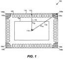
- FIG. 1shows a conventional semiconductor die.
- conventional die 100is rectangular and includes a number of bond pads, such as bond pad 102 (also referred to as “bond pads 102 ”), and core 104 .
- conventional die 100includes a number of “keep out zones,” such as keep out zones 106 a , 106 b , 106 c , and 106 d situated at corners 108 a , 108 b , 108 c , and 108 d , respectively.
- Each keep out zone in FIG. 1defines an area in which neither bond pads nor active circuitry may be placed.
- the large keep out zones of conventional die 100significantly reduces the usable area on the conventional semiconductor die.
- distance 118(also referred to as “R 1a ”) represents the distance from the center of conventional die 100 , i.e. center 114 , to corner 108 a and distance 116 (also referred to as “R 1b ”) represents the distance from center 114 to the center of side 110 situated at point 112 .
- R 1brepresents the shortest distance from center 114 to side 110 . Since the ratio R 1a /R 1b is significantly greater than 1.0, i.e.
- keep out zone 106 ais defined at corner 108 a to prevent malfunction or failure of the die as a result of high stresses imposed at corner 108 a .
- similar sized keep out zonesi.e. keep out zones 106 b , 106 c , and 106 d , are defined at the other corners of conventional die 100 .
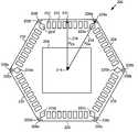
- FIG. 2shows a semiconductor die having increased usable area in accordance with one embodiment of the invention.
- hexagonal semiconductor die 200includes a number of bond pads, e.g. bond pad 202 (also referred to as “bond pads 202 ”), and core 204 .
- core 204has a square shape. In other embodiments, core 204 can have a rectangular or hexagonal shape, or any other appropriate shape.
- hexagonal semiconductor die 200has six sides, i.e. sides 222 , 224 , 226 , 228 , 230 , and 232 .
- semiconductor die 200can be a regular hexagon, i.e.
- hexagonal semiconductor die 200includes a number of keep out zones, such as keep out zones 206 a , 206 b , 206 c , 206 d , 206 e , and 206 f situated at corners 208 a , 208 b, 208 c , 208 d , 208 e , and 208 f , respectively.
- keep out zones 206 a , 206 b , 206 c , 206 d , 206 e , and 206 fsituated at corners 208 a , 208 b, 208 c , 208 d , 208 e , and 208 f , respectively.
- each keep out zone in FIG. 2defines an area in which neither bond pads nor active circuitry may be placed.
- Hexagonal semiconductor die 200 shown in FIG. 2can be conveniently diced using various die singulation processes.
- semiconductor die 200can be diced using water-jet-guided laser technology, which involves the use of a low-pressure water jet that guides a laser beam. The water prevents thermal damage to the die as the laser beam cuts through the wafer (not shown in FIG. 2 ). Accordingly, the water jet can be configured to follow the perimeter of semiconductor die 200 on a wafer to allow the laser to cut semiconductor die 200 .
- scribe linescan be formed around the six sided perimeter of semiconductor die 200 on a wafer. Thereafter, a number of perforations are formed within the scribe lines using a low power laser beam. After the perforations are made, tension can be applied to the wafer to separate semiconductor die 200 from the wafer. Regardless of the approach taken to form and dice semiconductor die 200 , it is manifest that the invention's semiconductor die 200 can be enclosed and used in various semiconductor packages after forming and dicing of the die.
- FIGS. 1 and 2can be used to compare the corner stress of conventional die 100 and hexagonal semiconductor die 200 .
- distance 218also referred to as “R 2a ” represents the distance from the center of semiconductor die 200 , i.e. center 214 , to corner 208 a and distance 216 (also referred to as “R 2b ”) represents the distance from center 214 to the center of side 222 situated at point 212 .
- R 2brepresents the shortest distance from center 214 to side 222 ;
- the ratio R 2a /R 2b for hexagonal semiconductor die 200 of the inventionis much closer to 1.0 compared to the ratio R 1a /R 1b for conventional die 100 shown in FIG.
- the stress suffered at the corners of semiconductor die 200is significantly lower than the stress suffered at the corners of conventional die 100 , e.g. the stress suffered at corner 108 a .
- the stress suffered at each corner of semiconductor die 200due to the reduced stress at each corner of semiconductor die 200 , keep out zones 206 a , 206 b , 206 c , 206 d, 206 e , and 206 f of semiconductor die 200 are each substantially smaller than the keep out zones of conventional die 100 , such as keep out zone 106 a in FIG. 1 .
- semiconductor die 200 of the inventionprovides more usable area than conventional die 100 .
- semiconductor die 200can provide a 5.0% increase in usable area over conventional die 100 .
- additional active circuitry or bond padsmay be included on the surface of hexagonal semiconductor die 200 , such as additional bond pads 220 a , 220 b , 220 c , 220 d, 220 e , and 220 f (hereinafter “bond pads 220 a through 220 f ”).
- additional bond pads 220 a through 220 fare diamond-shaped.
- bond pads 220 a through 220 fcan have any other suitable shapes or sizes.
- FIG. 3shows a semiconductor die having increased usable area in accordance with one embodiment of the invention.
- octagonal semiconductor die 300has eight sides, such as sides 302 and 304 .
- octagonal semiconductor die 300includes a number of keep out zones, such as keep out zones 306 a and 306 b , which are situated at corners 308 a and 308 b , respectively.
- keep out zones 306 a and 306 bwhich are situated at corners 308 a and 308 b , respectively.
- each keep out zone in FIG. 3defines an area in which neither bond pads nor active circuitry may be placed.
- octagonal semiconductor die 300also has smaller keep out zones than conventional die 100 in FIG. 1 , due to a further reduction of stress imposed at each corner of semiconductor die 300 .
- distance 316also referred to as “R 3a ” represents the distance from the center of semiconductor die 300 , i.e. center 312 , to corner 308 a and distance 314 (also referred to as “R 3b ”) represents the distance from center 312 to the center of side 302 situated at point 310 .
- R 3brepresents the shortest distance from center 312 to side 302 .
- the ratio R 3a /R 3b for semiconductor die 300is much closer to 1.0 compared to the ratio R 1a /R 1b for conventional die 100 , the stress suffered at the corners of octagonal semiconductor die 300 , e.g. the stress suffered at corner 308 a , is significantly lower than the stress suffered at the corners of conventional die 100 , e.g. the stress suffered at corner 108 a.
- the keep out zones of semiconductor 300e.g. keep out zones 306 a and 306 b
- the corners of a diegenerally represent its highest stress points.
- reduction of stress at the cornershas a profound effect on reducing die failure rate due to excessive stress imposed during, for example, semiconductor fabrication and packaging.
- potential sources of such imposed stressinclude probe card testing, die singulation, general die handling (such as “pick and place” processes), injection molding, wire bonding, and die packaging processes.
- a semiconductor die having six or eight sidesachieves substantially reduced stress at each corner of the die as compared to the stress at each corner of a conventional die.
- a semiconductor die with six or eight sidesadvantageously allows for substantially smaller keep out zones than a conventional four sided semiconductor die, such as conventional die 100 in FIG. 1 . Consequently, the six or eight sided-semiconductor dies of the present invention provide more usable area for bond pads or active circuitry than can be achieved with conventional dies.
- semiconductor dies having different number of sides that also result in a reduced corner stresscan be used in accordance with the teachings of the present invention.
Landscapes
- Physics & Mathematics (AREA)
- Condensed Matter Physics & Semiconductors (AREA)
- General Physics & Mathematics (AREA)
- Engineering & Computer Science (AREA)
- Computer Hardware Design (AREA)
- Microelectronics & Electronic Packaging (AREA)
- Power Engineering (AREA)
- Dicing (AREA)
Abstract
Description
Claims (19)
Priority Applications (1)
| Application Number | Priority Date | Filing Date | Title |
|---|---|---|---|
| US11/715,241US8193613B2 (en) | 2007-03-06 | 2007-03-06 | Semiconductor die having increased usable area |
Applications Claiming Priority (1)
| Application Number | Priority Date | Filing Date | Title |
|---|---|---|---|
| US11/715,241US8193613B2 (en) | 2007-03-06 | 2007-03-06 | Semiconductor die having increased usable area |
Publications (2)
| Publication Number | Publication Date |
|---|---|
| US20080220220A1 US20080220220A1 (en) | 2008-09-11 |
| US8193613B2true US8193613B2 (en) | 2012-06-05 |
Family
ID=39741933
Family Applications (1)
| Application Number | Title | Priority Date | Filing Date |
|---|---|---|---|
| US11/715,241Expired - Fee RelatedUS8193613B2 (en) | 2007-03-06 | 2007-03-06 | Semiconductor die having increased usable area |
Country Status (1)
| Country | Link |
|---|---|
| US (1) | US8193613B2 (en) |
Cited By (2)
| Publication number | Priority date | Publication date | Assignee | Title |
|---|---|---|---|---|
| US9911716B2 (en) | 2015-01-29 | 2018-03-06 | International Business Machines Corporation | Polygon die packaging |
| US11410894B2 (en) | 2019-09-06 | 2022-08-09 | International Business Machines Corporation | Polygon integrated circuit (IC) packaging |
Families Citing this family (6)
| Publication number | Priority date | Publication date | Assignee | Title |
|---|---|---|---|---|
| US8916980B2 (en)* | 2012-02-16 | 2014-12-23 | Omnivision Technologies, Inc. | Pad and circuit layout for semiconductor devices |
| GB201307773D0 (en) | 2013-04-30 | 2013-06-12 | Atlantic Inertial Systems Ltd | MEMS sensors |
| US9323972B2 (en)* | 2013-07-16 | 2016-04-26 | Apple Inc. | Finger biometric sensor including stacked die each having a non-rectangular shape and related methods |
| US10340306B1 (en)* | 2018-02-08 | 2019-07-02 | Semiconductor Components Industries, Llc | Semiconductor package with chamfered corners and related methods |
| CN116314040A (en)* | 2023-05-24 | 2023-06-23 | 深圳和美精艺半导体科技股份有限公司 | Bearing substrate and manufacturing method thereof |
| CN116403971A (en)* | 2023-06-08 | 2023-07-07 | 深圳和美精艺半导体科技股份有限公司 | IC packaging substrate |
Citations (15)
| Publication number | Priority date | Publication date | Assignee | Title |
|---|---|---|---|---|
| US4990462A (en)* | 1989-04-12 | 1991-02-05 | Advanced Micro Devices, Inc. | Method for coplanar integration of semiconductor ic devices |
| JPH03163817A (en)* | 1989-11-21 | 1991-07-15 | Mitsubishi Electric Corp | Large-scale semiconductor integrated circuit chip |
| US5539246A (en)* | 1995-03-01 | 1996-07-23 | Lsi Logic Corporation | Microelectronic integrated circuit including hexagonal semiconductor "gate " device |
| US5859448A (en)* | 1996-06-27 | 1999-01-12 | Sun Microsystems, Inc. | Alternative silicon chip geometries for integrated circuits |
| US6030885A (en)* | 1997-04-18 | 2000-02-29 | Vlsi Technology, Inc. | Hexagonal semiconductor die, semiconductor substrates, and methods of forming a semiconductor die |
| US6043134A (en)* | 1998-08-28 | 2000-03-28 | Micron Technology, Inc. | Semiconductor wafer alignment processes |
| US6153506A (en)* | 1999-03-08 | 2000-11-28 | Lucent Technologies Inc. | Integrated circuit having reduced probability of wire-bond failure |
| US6287949B1 (en)* | 1994-06-20 | 2001-09-11 | Fujitsu Limited | Multi-chip semiconductor chip module |
| US6407434B1 (en)* | 1994-11-02 | 2002-06-18 | Lsi Logic Corporation | Hexagonal architecture |
| US6500696B2 (en)* | 1999-10-14 | 2002-12-31 | Sun Microsystems, Inc. | Face to face chip |
| US6570243B1 (en)* | 1999-12-09 | 2003-05-27 | Sharp Kabushiki Kaisha | Dummy interconnects for suppressing thermally generated stress cracks |
| US6924210B1 (en)* | 2004-03-06 | 2005-08-02 | International Business Machines Corporation | Chip dicing |
| US20060278956A1 (en)* | 2003-03-13 | 2006-12-14 | Pdf Solutions, Inc. | Semiconductor wafer with non-rectangular shaped dice |
| US20100072578A1 (en)* | 2008-09-22 | 2010-03-25 | Nec Electronics Corporation | Semiconductor chip and semiconductor wafer |
| US7771532B2 (en)* | 2005-06-06 | 2010-08-10 | Sumitomo Electric Industries, Ltd. | Nitride semiconductor substrate and method of producing same |
- 2007
- 2007-03-06USUS11/715,241patent/US8193613B2/ennot_activeExpired - Fee Related
Patent Citations (15)
| Publication number | Priority date | Publication date | Assignee | Title |
|---|---|---|---|---|
| US4990462A (en)* | 1989-04-12 | 1991-02-05 | Advanced Micro Devices, Inc. | Method for coplanar integration of semiconductor ic devices |
| JPH03163817A (en)* | 1989-11-21 | 1991-07-15 | Mitsubishi Electric Corp | Large-scale semiconductor integrated circuit chip |
| US6287949B1 (en)* | 1994-06-20 | 2001-09-11 | Fujitsu Limited | Multi-chip semiconductor chip module |
| US6407434B1 (en)* | 1994-11-02 | 2002-06-18 | Lsi Logic Corporation | Hexagonal architecture |
| US5539246A (en)* | 1995-03-01 | 1996-07-23 | Lsi Logic Corporation | Microelectronic integrated circuit including hexagonal semiconductor "gate " device |
| US5859448A (en)* | 1996-06-27 | 1999-01-12 | Sun Microsystems, Inc. | Alternative silicon chip geometries for integrated circuits |
| US6030885A (en)* | 1997-04-18 | 2000-02-29 | Vlsi Technology, Inc. | Hexagonal semiconductor die, semiconductor substrates, and methods of forming a semiconductor die |
| US6043134A (en)* | 1998-08-28 | 2000-03-28 | Micron Technology, Inc. | Semiconductor wafer alignment processes |
| US6153506A (en)* | 1999-03-08 | 2000-11-28 | Lucent Technologies Inc. | Integrated circuit having reduced probability of wire-bond failure |
| US6500696B2 (en)* | 1999-10-14 | 2002-12-31 | Sun Microsystems, Inc. | Face to face chip |
| US6570243B1 (en)* | 1999-12-09 | 2003-05-27 | Sharp Kabushiki Kaisha | Dummy interconnects for suppressing thermally generated stress cracks |
| US20060278956A1 (en)* | 2003-03-13 | 2006-12-14 | Pdf Solutions, Inc. | Semiconductor wafer with non-rectangular shaped dice |
| US6924210B1 (en)* | 2004-03-06 | 2005-08-02 | International Business Machines Corporation | Chip dicing |
| US7771532B2 (en)* | 2005-06-06 | 2010-08-10 | Sumitomo Electric Industries, Ltd. | Nitride semiconductor substrate and method of producing same |
| US20100072578A1 (en)* | 2008-09-22 | 2010-03-25 | Nec Electronics Corporation | Semiconductor chip and semiconductor wafer |
Cited By (2)
| Publication number | Priority date | Publication date | Assignee | Title |
|---|---|---|---|---|
| US9911716B2 (en) | 2015-01-29 | 2018-03-06 | International Business Machines Corporation | Polygon die packaging |
| US11410894B2 (en) | 2019-09-06 | 2022-08-09 | International Business Machines Corporation | Polygon integrated circuit (IC) packaging |
Also Published As
| Publication number | Publication date |
|---|---|
| US20080220220A1 (en) | 2008-09-11 |
Similar Documents
| Publication | Publication Date | Title |
|---|---|---|
| US8193613B2 (en) | Semiconductor die having increased usable area | |
| US11037887B2 (en) | Method of making package assembly including stress relief structures | |
| US6818550B2 (en) | Method of cutting a wafer into individual chips | |
| US7554211B2 (en) | Semiconductor wafer and manufacturing process for semiconductor device | |
| US20080087989A1 (en) | Semiconductor device package of stacked semiconductor chips with spacers provided therein | |
| CN103021962B (en) | Semiconductor chip and processing method thereof | |
| US20050205975A1 (en) | Semiconductor package having step type die and method for manufacturing the same | |
| US7259043B2 (en) | Circular test pads on scribe street area | |
| US20170092552A1 (en) | Method for use in manufacturing a semiconductor device die | |
| US20090152683A1 (en) | Rounded die configuration for stress minimization and enhanced thermo-mechanical reliability | |
| JP2004055852A (en) | Semiconductor device and manufacturing method thereof | |
| US5119171A (en) | Semiconductor die having rounded or tapered edges and corners | |
| US7211500B2 (en) | Pre-process before cutting a wafer and method of cutting a wafer | |
| US20150214125A1 (en) | Scribe line structure | |
| US10128171B1 (en) | Leadframe with improved half-etch layout to reduce defects caused during singulation | |
| US20160181180A1 (en) | Packaged semiconductor device having attached chips overhanging the assembly pad | |
| US20110074003A1 (en) | Foil based semiconductor package | |
| US20080220206A1 (en) | Semiconductor die for increasing yield and usable wafer area | |
| US7955897B2 (en) | Chip structure and stacked chip package as well as method for manufacturing chip structures | |
| JPS59220947A (en) | Manufacture of semiconductor device | |
| US9875913B2 (en) | Method for singulating packaged integrated circuits and resulting structures | |
| JP2005302985A (en) | Semiconductor wafer and semiconductor chip | |
| US10818550B2 (en) | Methods for singulation and packaging | |
| CN101924039B (en) | Semiconductor package and manufacturing method thereof | |
| US8241960B2 (en) | Semiconductor device manufacturing equipment and semiconductor device manufacturing method |
Legal Events
| Date | Code | Title | Description |
|---|---|---|---|
| AS | Assignment | Owner name:BROADCOM CORPORATION, CALIFORNIA Free format text:ASSIGNMENT OF ASSIGNORS INTEREST;ASSIGNORS:WANG, KEN JIAN MING;SZE, MING WANG;REEL/FRAME:019052/0590 Effective date:20070305 | |
| REMI | Maintenance fee reminder mailed | ||
| AS | Assignment | Owner name:BANK OF AMERICA, N.A., AS COLLATERAL AGENT, NORTH CAROLINA Free format text:PATENT SECURITY AGREEMENT;ASSIGNOR:BROADCOM CORPORATION;REEL/FRAME:037806/0001 Effective date:20160201 Owner name:BANK OF AMERICA, N.A., AS COLLATERAL AGENT, NORTH Free format text:PATENT SECURITY AGREEMENT;ASSIGNOR:BROADCOM CORPORATION;REEL/FRAME:037806/0001 Effective date:20160201 | |
| LAPS | Lapse for failure to pay maintenance fees | ||
| STCH | Information on status: patent discontinuation | Free format text:PATENT EXPIRED DUE TO NONPAYMENT OF MAINTENANCE FEES UNDER 37 CFR 1.362 | |
| FP | Lapsed due to failure to pay maintenance fee | Effective date:20160605 | |
| AS | Assignment | Owner name:AVAGO TECHNOLOGIES GENERAL IP (SINGAPORE) PTE. LTD., SINGAPORE Free format text:ASSIGNMENT OF ASSIGNORS INTEREST;ASSIGNOR:BROADCOM CORPORATION;REEL/FRAME:041706/0001 Effective date:20170120 Owner name:AVAGO TECHNOLOGIES GENERAL IP (SINGAPORE) PTE. LTD Free format text:ASSIGNMENT OF ASSIGNORS INTEREST;ASSIGNOR:BROADCOM CORPORATION;REEL/FRAME:041706/0001 Effective date:20170120 | |
| AS | Assignment | Owner name:BROADCOM CORPORATION, CALIFORNIA Free format text:TERMINATION AND RELEASE OF SECURITY INTEREST IN PATENTS;ASSIGNOR:BANK OF AMERICA, N.A., AS COLLATERAL AGENT;REEL/FRAME:041712/0001 Effective date:20170119 |