US8191237B1 - Method for providing a structure in a magnetic transducer - Google Patents
Method for providing a structure in a magnetic transducerDownload PDFInfo
- Publication number
- US8191237B1 US8191237B1US12/470,385US47038509AUS8191237B1US 8191237 B1US8191237 B1US 8191237B1US 47038509 AUS47038509 AUS 47038509AUS 8191237 B1US8191237 B1US 8191237B1
- Authority
- US
- United States
- Prior art keywords
- planarization
- buffer layer
- cmp
- layer
- thickness
- Prior art date
- Legal status (The legal status is an assumption and is not a legal conclusion. Google has not performed a legal analysis and makes no representation as to the accuracy of the status listed.)
- Expired - Fee Related, expires
Links
- 238000000034methodMethods0.000titleclaimsabstractdescription58
- HBMJWWWQQXIZIP-UHFFFAOYSA-Nsilicon carbideChemical compound[Si+]#[C-]HBMJWWWQQXIZIP-UHFFFAOYSA-N0.000claimsdescription7
- 229910010271silicon carbideInorganic materials0.000claimsdescription7
- TWNQGVIAIRXVLR-UHFFFAOYSA-Noxo(oxoalumanyloxy)alumaneChemical compoundO=[Al]O[Al]=OTWNQGVIAIRXVLR-UHFFFAOYSA-N0.000claimsdescription5
- OKTJSMMVPCPJKN-UHFFFAOYSA-NCarbonChemical compound[C]OKTJSMMVPCPJKN-UHFFFAOYSA-N0.000claimsdescription4
- 229910052799carbonInorganic materials0.000claimsdescription4
- 239000000126substanceSubstances0.000claimsdescription4
- 150000002500ionsChemical class0.000claimsdescription3
- 238000005530etchingMethods0.000claims1
- 238000001020plasma etchingMethods0.000claims1
- 238000007796conventional methodMethods0.000description8
- 230000015572biosynthetic processEffects0.000description5
- 238000004519manufacturing processMethods0.000description5
- PNEYBMLMFCGWSK-UHFFFAOYSA-Naluminium oxideInorganic materials[O-2].[O-2].[O-2].[Al+3].[Al+3]PNEYBMLMFCGWSK-UHFFFAOYSA-N0.000description4
- 238000000151depositionMethods0.000description4
- 229920002120photoresistant polymerPolymers0.000description4
- 239000000696magnetic materialSubstances0.000description3
- 238000000992sputter etchingMethods0.000description3
- 230000002411adverseEffects0.000description2
- 238000010586diagramMethods0.000description2
- 239000002002slurrySubstances0.000description2
- IERHLVCPSMICTF-XVFCMESISA-NCMP groupChemical groupP(=O)(O)(O)OC[C@@H]1[C@H]([C@H]([C@@H](O1)N1C(=O)N=C(N)C=C1)O)OIERHLVCPSMICTF-XVFCMESISA-N0.000description1
- 239000013317conjugated microporous polymerSubstances0.000description1
- 230000008021depositionEffects0.000description1
- 210000003643myeloid progenitor cellAnatomy0.000description1
Images


Classifications
- G—PHYSICS
- G11—INFORMATION STORAGE
- G11B—INFORMATION STORAGE BASED ON RELATIVE MOVEMENT BETWEEN RECORD CARRIER AND TRANSDUCER
- G11B5/00—Recording by magnetisation or demagnetisation of a record carrier; Reproducing by magnetic means; Record carriers therefor
- G11B5/127—Structure or manufacture of heads, e.g. inductive
- G11B5/31—Structure or manufacture of heads, e.g. inductive using thin films
- G11B5/3163—Fabrication methods or processes specially adapted for a particular head structure, e.g. using base layers for electroplating, using functional layers for masking, using energy or particle beams for shaping the structure or modifying the properties of the basic layers
- G—PHYSICS
- G11—INFORMATION STORAGE
- G11B—INFORMATION STORAGE BASED ON RELATIVE MOVEMENT BETWEEN RECORD CARRIER AND TRANSDUCER
- G11B5/00—Recording by magnetisation or demagnetisation of a record carrier; Reproducing by magnetic means; Record carriers therefor
- G11B5/127—Structure or manufacture of heads, e.g. inductive
- G11B5/1278—Structure or manufacture of heads, e.g. inductive specially adapted for magnetisations perpendicular to the surface of the record carrier
- G—PHYSICS
- G11—INFORMATION STORAGE
- G11B—INFORMATION STORAGE BASED ON RELATIVE MOVEMENT BETWEEN RECORD CARRIER AND TRANSDUCER
- G11B5/00—Recording by magnetisation or demagnetisation of a record carrier; Reproducing by magnetic means; Record carriers therefor
- G11B5/127—Structure or manufacture of heads, e.g. inductive
- G11B5/31—Structure or manufacture of heads, e.g. inductive using thin films
- G11B5/3109—Details
- G11B5/3116—Shaping of layers, poles or gaps for improving the form of the electrical signal transduced, e.g. for shielding, contour effect, equalizing, side flux fringing, cross talk reduction between heads or between heads and information tracks
- G—PHYSICS
- G11—INFORMATION STORAGE
- G11B—INFORMATION STORAGE BASED ON RELATIVE MOVEMENT BETWEEN RECORD CARRIER AND TRANSDUCER
- G11B5/00—Recording by magnetisation or demagnetisation of a record carrier; Reproducing by magnetic means; Record carriers therefor
- G11B5/127—Structure or manufacture of heads, e.g. inductive
- G11B5/31—Structure or manufacture of heads, e.g. inductive using thin films
- G11B5/3109—Details
- G11B5/313—Disposition of layers
- G11B5/3143—Disposition of layers including additional layers for improving the electromagnetic transducing properties of the basic structure, e.g. for flux coupling, guiding or shielding
- G11B5/3146—Disposition of layers including additional layers for improving the electromagnetic transducing properties of the basic structure, e.g. for flux coupling, guiding or shielding magnetic layers
- G11B5/315—Shield layers on both sides of the main pole, e.g. in perpendicular magnetic heads
- Y—GENERAL TAGGING OF NEW TECHNOLOGICAL DEVELOPMENTS; GENERAL TAGGING OF CROSS-SECTIONAL TECHNOLOGIES SPANNING OVER SEVERAL SECTIONS OF THE IPC; TECHNICAL SUBJECTS COVERED BY FORMER USPC CROSS-REFERENCE ART COLLECTIONS [XRACs] AND DIGESTS
- Y10—TECHNICAL SUBJECTS COVERED BY FORMER USPC
- Y10T—TECHNICAL SUBJECTS COVERED BY FORMER US CLASSIFICATION
- Y10T29/00—Metal working
- Y10T29/49—Method of mechanical manufacture
- Y10T29/49002—Electrical device making
- Y10T29/4902—Electromagnet, transformer or inductor
- Y10T29/49021—Magnetic recording reproducing transducer [e.g., tape head, core, etc.]
- Y10T29/49032—Fabricating head structure or component thereof
- Y10T29/49036—Fabricating head structure or component thereof including measuring or testing
- Y10T29/49043—Depositing magnetic layer or coating
- Y10T29/49044—Plural magnetic deposition layers
- Y—GENERAL TAGGING OF NEW TECHNOLOGICAL DEVELOPMENTS; GENERAL TAGGING OF CROSS-SECTIONAL TECHNOLOGIES SPANNING OVER SEVERAL SECTIONS OF THE IPC; TECHNICAL SUBJECTS COVERED BY FORMER USPC CROSS-REFERENCE ART COLLECTIONS [XRACs] AND DIGESTS
- Y10—TECHNICAL SUBJECTS COVERED BY FORMER USPC
- Y10T—TECHNICAL SUBJECTS COVERED BY FORMER US CLASSIFICATION
- Y10T29/00—Metal working
- Y10T29/49—Method of mechanical manufacture
- Y10T29/49002—Electrical device making
- Y10T29/4902—Electromagnet, transformer or inductor
- Y10T29/49021—Magnetic recording reproducing transducer [e.g., tape head, core, etc.]
- Y10T29/49032—Fabricating head structure or component thereof
- Y10T29/49036—Fabricating head structure or component thereof including measuring or testing
- Y10T29/49043—Depositing magnetic layer or coating
- Y10T29/49046—Depositing magnetic layer or coating with etching or machining of magnetic material
- Y—GENERAL TAGGING OF NEW TECHNOLOGICAL DEVELOPMENTS; GENERAL TAGGING OF CROSS-SECTIONAL TECHNOLOGIES SPANNING OVER SEVERAL SECTIONS OF THE IPC; TECHNICAL SUBJECTS COVERED BY FORMER USPC CROSS-REFERENCE ART COLLECTIONS [XRACs] AND DIGESTS
- Y10—TECHNICAL SUBJECTS COVERED BY FORMER USPC
- Y10T—TECHNICAL SUBJECTS COVERED BY FORMER US CLASSIFICATION
- Y10T29/00—Metal working
- Y10T29/49—Method of mechanical manufacture
- Y10T29/49002—Electrical device making
- Y10T29/4902—Electromagnet, transformer or inductor
- Y10T29/49021—Magnetic recording reproducing transducer [e.g., tape head, core, etc.]
- Y10T29/49032—Fabricating head structure or component thereof
- Y10T29/49048—Machining magnetic material [e.g., grinding, etching, polishing]
- Y10T29/49052—Machining magnetic material [e.g., grinding, etching, polishing] by etching
Definitions
- FIG. 1is a flow chart depicting a conventional method 10 for fabricating a conventional perpendicular magnetic recording (PMR) transducer. For simplicity, some steps are omitted.
- the conventional method 10is used for providing a PMR pole.
- the film stack for the poleis deposited, via step 12 .
- Step 12generally includes depositing seed layer(s), high moment magnetic film(s), a chemical mechanical planarization (CMP) stop layer, and one or more hard mask layers.
- a pattern in the hard mask layer(s)is provided, via step 14 .
- Step 14may include providing a photoresist mask and transferring the pattern of the photoresist mask to the hard mask layer(s). The photoresist mask pattern may be transferred by ion milling.
- the poleis then defined from the high moment magnetic layers, via step 18 .
- Step 18may also be performed by ion milling through the high moment magnetic layers.
- the PMR pole formedhas a negative angle, with its top being wider than its bottom.
- the transduceris then refilled with alumina, via step 20 .
- the regions around the polemay be filled.
- the top surface of the transducermay not be even. Consequently, a CMP may be performed, via step 22 .
- the CMPtypically terminates when at least a portion of the CMP stop layer remains.
- the CMP stop layeris then removed, for example using a reactive ion etch (RIE). Fabrication of the magnetic transducer may then be completed.
- RIEreactive ion etch
- the conventional methodfunctions, there are inconsistencies in fabrication of the transducer. These inconsistencies may adversely affect both the yield of the conventional method 10 and the performance of poles formed using the conventional method 10 .
- the CMPmay result in dishing and/or similar nonuniformities.
- the top surface of the transducermay not be as flat as desired. Formation of subsequent structures, such as shields, may be adversely affected. Performance of the transducer provided and yield of the method 10 may thus be affected.
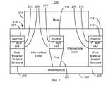
- a method and system for providing a structure in a magnetic transducerare described.
- the transduceralso includes an additional structure distal from the structure, a first planarization buffer layer, and an intermediate layer.
- a first portion of the first planarization buffer layerresides on the structure.
- a second portion of the first planarization buffer layerresides on the additional structure.
- a first portion of the intermediate layerresides between the structure and the additional structure.
- a second portion of the intermediate layerresides above the structure.
- the method and systeminclude performing a first planarization that exposes a top surface of the magnetic transducer and terminates before a portion of the first planarization buffer layer is removed.
- the method and systemalso include providing a second planarization buffer layer having a top and residing above the first planarization buffer layer.
- the second planarization buffer layeris provided after the first planarization is terminated. A second planarization is performed. The second planarization terminates before the second planarization buffer layer is completely removed.
- the method and systemalso include performing a third planarization terminating after the first planarization buffer layer is exposed and before the first planarization buffer layer is completely removed.
- FIG. 1is a flow chart depicting a conventional method for fabricating a PMR head.
- FIG. 2is a flow chart depicting an exemplary embodiment of a method for fabricating a structure in a magnetic transducer.
- FIG. 3is a flow chart depicting another embodiment of a method for fabricating a PMR transducer.
- FIGS. 4-12are diagrams depicting an exemplary embodiment of a perpendicular magnetic recording transducer during fabrication.
- FIG. 2is a flow chart depicting an exemplary embodiment of a method 100 for fabricating a structure for a magnetic recording transducer.
- the structure describedmay include a PMR pole. However, other structures may also be fabricated. For simplicity, some steps may be omitted.
- the transducer being fabricatedmay be part of a merged head that includes read and write head and resides on a slider in a disk drive.
- the method 100also may commence after formation of other portions of the transducer.
- the method 100is also described in the context of providing a single structure in a single magnetic recording transducer. However, the method 100 may be used to fabricate multiple structure and/or multiple transducers at substantially the same time.
- the method 100 and systemare also described in the context of particular layers. However, in some embodiments, such layers may include multiple sub-layers.
- the method 100commences after formation of some structures in the transducer have been fabricated.
- the method 100starts after the structure has been defined.
- a PMR polea PMR pole stack including magnetic materials and a first planarization buffer layer is deposited and the PMR pole defined from the stack.
- a planarization buffer layeris one which slows or stops the planarization. Stated differently, the layer is more difficult to remove using the planarization step.
- this additional structureis a CMP or other planarization support structure.
- the first planarization buffer layerhas a thickness of at least thirty and not more than fifty nanometers. In another embodiment, the first planarization buffer layer may be thinner, for example as thin as ten nanometers.
- one or more hard mask layersmay be part of the stack.
- the method 100may also start after component(s) other than the structure have been formed. For example, an intermediate layer, such as aluminum oxide, may also have been provided. The intermediate layer may cover the structure, reside between the structure and the additional structures, and reside on top of the additional structure(s). Thus, the structure/PMR pole and additional structure may both reside under portions of the intermediate layer. However, the top surface of the transducer would have a topology that reflects the discontinuity of underlying layers instead of being flat.
- a first planarizationis performed, via step 102 .
- the first planarizationexposes a new top surface of the magnetic transducer and terminates before the first planarization buffer layer is removed.
- first planarizationremoves part of the intermediate layer and ensures that the top surface is more uniform and substantially flat.
- This planarizationmay be a CMP configured to planarized aluminum oxide.
- a mask that covers the structureis optionally provided, via step 104 .
- the bottom of the maskwould be on the top surface of the magnetic transducer that was exposed in step 102 .
- the maskwould expose part of the transducer including the additional structure(s).
- the exposed portion of the magnetic transduceris optionally etched, via step 106 . The etch removes part of the intermediate and other layer(s), but does not remove the first planarization buffer layer.
- steps 104 and 106may be performed in a different manner or might be omitted.
- a second planarization buffer layeris provided, via step 106 .
- a planarization buffer layeris a layer which slows or stops a planarization step.
- the second planarization buffer layermight include diamond-like carbon (DLC), silicon carbide, Ru, and/or Cr where the second planarization (described below) is a CMP step.
- the second planarization buffer layermay also be configured to be removable using a different process than the first planarization buffer layer. For example, if both the first and second planarization buffer layers are for CMPs, one of the buffer layers may be silicon carbide while the other is DLC.
- the second planarization buffer layeris on the additional structure(s), but not on the structure.
- the thickness of the second planarization buffer layeris also set based on the first planarization buffer layer. For example, suppose the first planarization buffer layer has a first thickness, the second planarization buffer layer has a second thickness, and the intermediate layer has a third thickness.
- the second thickness of the second planarization buffer layeris greater than the first thickness of the first planarization buffer layer and less than the third thickness of the intermediate layer.
- the second planarization buffer layerhas a thickness of at least fifty and not more than one hundred fifty nanometers.
- the portion of the second planarization buffer layer on the additional structureis below the bottom of the mask.
- the maskmay also be removed in step 106 after deposition of the second planarization buffer layer. After the second planarization buffer layer is provided and the mask removed, the portion of the transducer above the structure would protrude slightly beyond the second planarization buffer layer.
- a second planarizationis performed, via step 110 .
- the second planarizationterminates before the second planarization buffer layer is completely removed.
- the top surface of the transduceris, again, substantially flat.
- the remaining part of the second planarization buffer layer around the structuremay protrude slightly.
- a remaining portion of the second planarization buffer layermay optionally be removed after the second planarization is terminated, via step 112 .
- the second planarization buffer layeris removed in step 112 substantially without removing any portion of the first planarization buffer layer.
- a RIE with a chemistry appropriate for the second planarization buffer layermay be performed in step 112 .
- the first planarization buffer layermay be removable by another RIE using a different chemistry.
- step 114may include providing a mask covering the structure and exposing the additional structure, then performing the RIE.
- step 112may be omitted.
- a third planarization buffer layermay optionally be provided in step 114 .
- the third planarization buffer layerwould be below the top of the remaining intermediate layer on the structure.
- the third planarization buffer layeris also desired to be thinner than the second planarization buffer layer and thicker than the first planarization buffer layer.
- the portion of the transducer above the structuremay protrude slightly. However, it protrudes less than after step 108 .
- step 114may be omitted.
- a third planarizationis optionally performed, via step 116 .
- the third planarizationis terminated before the third planarization buffer layer is completely removed.
- step 116also includes removing any remaining third planarization buffer layer.
- step 116may be omitted.
- a fourth planarizationis performed, via step 118 .
- step 118includes performing a CMP.
- the fourth planarizationterminates after the first planarization buffer layer is exposed and before the first planarization buffer layer is completely removed.
- the first planarization buffer layermay be thinner than the second and third planarization buffer layers.
- the fourth planarizationmay be designed to remove only a small portion of the transducer.
- a touch planarizationmay thus be used in step 118 . Stated differently, the fourth planarization may be short in duration, use a dilute slurry, and/or a lower pressure.
- the transducer having a flat top surfacemay be formed around the structure.
- the variations in the top surfacemay be reduced over that of the conventional method 10 described in FIG. 1 .
- Better control of the topology of the transducer, as well as subsequent structures,may thus be achieved.
- Yieldmay likewise be improved.
- four planarizations and three bufferare described, another number of planarizations and another number of planarization buffer layers may be used. The process of thinner protrusions and buffer layers and lighter planarizations may relatively simply and easily improve the uniformity of the device being provided. Thus, yield, performance and uniformity may be improved.
- FIG. 3is a flow chart depicting an exemplary embodiment of a method 150 for fabricating a PMR pole for a magnetic recording transducer.
- the method 150is analogous to the method 100 .
- the structure being fabricatedis a PMR pole.
- some stepsmay be omitted.
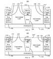
- FIGS. 4-12are diagrams depicting an exemplary embodiment of a perpendicular magnetic recording transducer 200 during fabrication. For clarity, FIGS. 4-12 are not to scale. Referring to FIGS. 3-12 , the method 150 is described in the context of the PMR transducer 200 .
- the PMR transducer 200 being fabricatedmay be part of a merged head that also includes read transducer and resides on a slider in a disk drive.
- the method 150also may commence after formation of other portions of the PMR transducer 200 .
- the method 150is also described in the context of providing a single PMR pole in a single magnetic recording transducer. However, the method 150 may be used to fabricate multiple PMR poles and/or multiple transducers at substantially the same time.
- the method 150 and systemare also described in the context of particular layers. However, in some embodiments, such layers may include multiple sub-layers.
- the method 150commences after formation of some structures in the transducer have been fabricated. For example, in one embodiment, the method 150 starts after the PMR pole stack including magnetic materials and a first planarization buffer layer has been deposited. In one embodiment, the first planarization buffer layer is on the order of fifty nanometers or less in thickness. In one such embodiment, the first planarization buffer layer is at least thirty nanometers thick.
- Step 152may be performed by ion milling the PMR transducer with the hard mask(s) and any other mask(s) desired, in place.
- FIG. 4depicts the PMR transducer after step 152 is performed. Consequently, the PMR pole 204 and support structures 206 are shown on the underlayer 202 .
- the distance between the support structures 206 and the edges of the PMR pole 204may be at least three times the height of the PMR pole 204 .
- the PMR pole 204is 0.3 micrometers thick.
- the support structures 206may be spaced approximately one micrometer from the PMR pole 204 .
- the hard mask(s) 208are shown.
- first planarization buffer layer 210which was deposited as part of the stack, is shown.
- the first planarization buffer layeris also desired to be thin.
- the first planarization buffer layer 210may be not more than fifty nanometers in thickness.
- a top, nonmagnetic layer, shown in FIG. 4 as alumina 212is also present. Both the PMR pole 204 and additional structures 206 distal from the PMR pole 204 are formed.
- Step 154may thus include depositing alumina and/or other nonmagnetic layers to refill the regions around the PMR pole 204 .
- FIG. 5depicts the PMR transducer 200 after step 154 is performed. Consequently, the intermediate layer 214 is shown.
- the intermediate layer 214resides not only on the PMR pole 204 and support structures 206 , but also in the region between the PMR pole 204 and support structures 206 .
- the intermediate layer 214is thicker than the combination of the PMR pole 204 and additional structures 208 , 210 , and 212 .
- the intermediate layer 214may be at least one and not more than ten micrometers thick. In one such embodiment, the intermediate layer 214 is at least five micrometers thick.
- a first CMPis performed, via step 156 .
- This planarizationmay be a CMP configured to planarized aluminum oxide.
- the first planarizationexposes a new, top surface of the PMR transducer 200 and terminates before the first planarization buffer layer 210 is removed.
- FIG. 6depicts the PMR transducer 200 after step 156 is performed.
- the first planarizationhas thus removed part of the intermediate layer 214 .
- the remaining portion of the intermediate layer 214 ′has a newly exposed top surface 215 that is uniform and substantially flat.
- a mask that covers the PMR pole 204is provided, via step 158 .
- the support structures 206are, however, exposed.
- the mask provided in step 158is a photoresist mask.
- FIG. 7depicts the PMR transducer 200 after step 158 is performed. The mask 216 is thus shown. The bottom of the mask 216 is on the top surface 215 of the magnetic transducer that was exposed in step 158 .
- the mask 216covers not only the PMR pole 204 , but also at least part of the region between the PMR pole 204 and the support structures 206 .
- the mask 216exposes part of the transducer including the additional/support structure(s) 206 .
- step 160includes performing an aluminum oxide RIE.
- the remaining intermediate layer 214 ′ in exposed regions above the support structure 206is thinner than the portion of the intermediate layer 214 ′ under the mask 216 .
- a second planarization buffer layeris provided, via step 162 .
- step 162may include depositing one or more of DLC, silicon carbide, Ru, and Cr.
- the second planarization buffer layermay also be configured to be removable using a different process than the first planarization buffer layer.
- the first planarization buffer layeris silicon carbide the second planarization buffer layer may be DLC.
- the maskmay also be removed in step 162 . For example, a lift-off may be performed.
- FIG. 8depicts the PMR transducer 200 after step 160 has been performed and the second planarization buffer layer has been deposited in step 162 .
- the remaining portion of the intermediate layer 214 ′′is beneath the mask 216 .
- the rest of the intermediate layer 214 ′′has been removed.
- the alumina layer 212(not shown) has been removed from the exposed portions of the PMR transducer.
- the second planarization buffer layer 218has been provided. Because of the presence of the mask 216 , the second planarization buffer layer 218 resides above the support structure.
- the second planarization buffer layer 218has its thickness set such that the top of the second planarization buffer layer 218 is below the bottom of the mask 216 and thus below the top of the intermediate layer 214 ′′. In one embodiment, the second planarization buffer layer 218 has a thickness of at least ten and not more than one hundred fifty nanometers. In one such embodiment, the thickness of the second planarization buffer layer 218 is at least fifty nanometers and not more than one hundred and fifty nanometers.
- FIG. 9depicts the transducer 200 after step 162 is completed and the mask 216 has been removed. Thus, only the portion of the second planarization buffer layer 218 ′ on the support structures 206 remains. Because the second planarization buffer layer 218 ′ is sufficiently thin, the portion of the transducer 200 that was under the mask 216 (not shown in FIG. 9 ) protrudes slightly beyond the second planarization buffer layer 218 ′′
- a second planarizationis performed, via step 164 .
- the second planarizationterminates before the second planarization buffer layer 218 ′ is completely removed.
- FIG. 10depicts the PMR transducer 200 after step 164 has been performed.
- the top surface of the intermediate layer 214 ′′′ for the PMR transducer 200is, again, substantially flat.
- the top of the second buffer layer 218 ′is slightly above the top of the intermediate layer 214 ′′′. This is because the second buffer layer 218 ′ is polished away more slowly than the intermediate layer 214 ′′′.
- step 166includes performing a RIE with the appropriate chemistry for removing the second planarization buffer layer 218 ′.
- FIG. 11depicts the PMR transducer 200 after step 166 is performed.
- the intermediate layer 214 ′′′ of the transducer around the PMR pole 204may again protrude slightly. However, the protrusion is less than after step 160 .
- a third CMPis performed, via step 168 .
- the third planarizationterminates after the first planarization buffer layer 210 is exposed and before the first planarization buffer layer 210 is completely removed.
- a touch planarizationmay thus be used in step 168 .
- the third planarizationmay be short in duration, use a dilute slurry, and/or a lower pressure.
- FIG. 12depicts the PMR transducer 200 after step 168 is performed.
- the first planarization buffer layer 210is thinner than the second planarization buffer layer 218 ′.
- the third planarizationmay be designed to remove only a small portion of the intermediate layer 214 ′′.
- tops surface of the intermediate layer 214 ′′′is thus at substantially the same height as the remaining portion of the first planarization buffer layer 210 . Fabrication of the PMR transducer 200 may then be completed. For example, a top shield (not shown), which may be desired to be flat or controllable, may be provided
- the PMR transducer 200 having a flat top surfacemay be formed around the structure.
- the variations in the top surfacemay be reduced over that of the conventional method 10 described in FIG. 1 .
- Better control of the topology of the transducer, as well as subsequent structures,may thus be achieved. Yield may likewise be improved.
- the process of planarizations using progressively thinner planarization buffer layersmay be extended to more buffer layers and/or more planarizations. Consequently, further uniformity may be achieved.
Landscapes
- Engineering & Computer Science (AREA)
- Manufacturing & Machinery (AREA)
- Physics & Mathematics (AREA)
- Electromagnetism (AREA)
- Magnetic Heads (AREA)
Abstract
Description
Claims (16)
Priority Applications (1)
| Application Number | Priority Date | Filing Date | Title |
|---|---|---|---|
| US12/470,385US8191237B1 (en) | 2009-05-21 | 2009-05-21 | Method for providing a structure in a magnetic transducer |
Applications Claiming Priority (1)
| Application Number | Priority Date | Filing Date | Title |
|---|---|---|---|
| US12/470,385US8191237B1 (en) | 2009-05-21 | 2009-05-21 | Method for providing a structure in a magnetic transducer |
Publications (1)
| Publication Number | Publication Date |
|---|---|
| US8191237B1true US8191237B1 (en) | 2012-06-05 |
Family
ID=46147930
Family Applications (1)
| Application Number | Title | Priority Date | Filing Date |
|---|---|---|---|
| US12/470,385Expired - Fee RelatedUS8191237B1 (en) | 2009-05-21 | 2009-05-21 | Method for providing a structure in a magnetic transducer |
Country Status (1)
| Country | Link |
|---|---|
| US (1) | US8191237B1 (en) |
Cited By (131)
| Publication number | Priority date | Publication date | Assignee | Title |
|---|---|---|---|---|
| US8830628B1 (en) | 2009-02-23 | 2014-09-09 | Western Digital (Fremont), Llc | Method and system for providing a perpendicular magnetic recording head |
| US8879207B1 (en) | 2011-12-20 | 2014-11-04 | Western Digital (Fremont), Llc | Method for providing a side shield for a magnetic recording transducer using an air bridge |
| US8883017B1 (en) | 2013-03-12 | 2014-11-11 | Western Digital (Fremont), Llc | Method and system for providing a read transducer having seamless interfaces |
| US8917581B1 (en) | 2013-12-18 | 2014-12-23 | Western Digital Technologies, Inc. | Self-anneal process for a near field transducer and chimney in a hard disk drive assembly |
| US8923102B1 (en) | 2013-07-16 | 2014-12-30 | Western Digital (Fremont), Llc | Optical grating coupling for interferometric waveguides in heat assisted magnetic recording heads |
| US8947985B1 (en) | 2013-07-16 | 2015-02-03 | Western Digital (Fremont), Llc | Heat assisted magnetic recording transducers having a recessed pole |
| US8953422B1 (en) | 2014-06-10 | 2015-02-10 | Western Digital (Fremont), Llc | Near field transducer using dielectric waveguide core with fine ridge feature |
| US8958272B1 (en) | 2014-06-10 | 2015-02-17 | Western Digital (Fremont), Llc | Interfering near field transducer for energy assisted magnetic recording |
| US8970988B1 (en) | 2013-12-31 | 2015-03-03 | Western Digital (Fremont), Llc | Electric gaps and method for making electric gaps for multiple sensor arrays |
| US8971160B1 (en) | 2013-12-19 | 2015-03-03 | Western Digital (Fremont), Llc | Near field transducer with high refractive index pin for heat assisted magnetic recording |
| US8976635B1 (en) | 2014-06-10 | 2015-03-10 | Western Digital (Fremont), Llc | Near field transducer driven by a transverse electric waveguide for energy assisted magnetic recording |
| US8980109B1 (en) | 2012-12-11 | 2015-03-17 | Western Digital (Fremont), Llc | Method for providing a magnetic recording transducer using a combined main pole and side shield CMP for a wraparound shield scheme |
| US8982508B1 (en) | 2011-10-31 | 2015-03-17 | Western Digital (Fremont), Llc | Method for providing a side shield for a magnetic recording transducer |
| US8984740B1 (en) | 2012-11-30 | 2015-03-24 | Western Digital (Fremont), Llc | Process for providing a magnetic recording transducer having a smooth magnetic seed layer |
| US8988825B1 (en) | 2014-02-28 | 2015-03-24 | Western Digital (Fremont, LLC | Method for fabricating a magnetic writer having half-side shields |
| US8988812B1 (en) | 2013-11-27 | 2015-03-24 | Western Digital (Fremont), Llc | Multi-sensor array configuration for a two-dimensional magnetic recording (TDMR) operation |
| US8995087B1 (en) | 2006-11-29 | 2015-03-31 | Western Digital (Fremont), Llc | Perpendicular magnetic recording write head having a wrap around shield |
| US8993217B1 (en) | 2013-04-04 | 2015-03-31 | Western Digital (Fremont), Llc | Double exposure technique for high resolution disk imaging |
| US8997832B1 (en) | 2010-11-23 | 2015-04-07 | Western Digital (Fremont), Llc | Method of fabricating micrometer scale components |
| US9001628B1 (en) | 2013-12-16 | 2015-04-07 | Western Digital (Fremont), Llc | Assistant waveguides for evaluating main waveguide coupling efficiency and diode laser alignment tolerances for hard disk |
| US9001467B1 (en) | 2014-03-05 | 2015-04-07 | Western Digital (Fremont), Llc | Method for fabricating side shields in a magnetic writer |
| US9007719B1 (en) | 2013-10-23 | 2015-04-14 | Western Digital (Fremont), Llc | Systems and methods for using double mask techniques to achieve very small features |
| US9007879B1 (en) | 2014-06-10 | 2015-04-14 | Western Digital (Fremont), Llc | Interfering near field transducer having a wide metal bar feature for energy assisted magnetic recording |
| US9007725B1 (en) | 2014-10-07 | 2015-04-14 | Western Digital (Fremont), Llc | Sensor with positive coupling between dual ferromagnetic free layer laminates |
| US9013836B1 (en) | 2013-04-02 | 2015-04-21 | Western Digital (Fremont), Llc | Method and system for providing an antiferromagnetically coupled return pole |
| US9042208B1 (en) | 2013-03-11 | 2015-05-26 | Western Digital Technologies, Inc. | Disk drive measuring fly height by applying a bias voltage to an electrically insulated write component of a head |
| US9042051B2 (en) | 2013-08-15 | 2015-05-26 | Western Digital (Fremont), Llc | Gradient write gap for perpendicular magnetic recording writer |
| US9042052B1 (en) | 2014-06-23 | 2015-05-26 | Western Digital (Fremont), Llc | Magnetic writer having a partially shunted coil |
| US9042058B1 (en) | 2013-10-17 | 2015-05-26 | Western Digital Technologies, Inc. | Shield designed for middle shields in a multiple sensor array |
| US9042057B1 (en) | 2013-01-09 | 2015-05-26 | Western Digital (Fremont), Llc | Methods for providing magnetic storage elements with high magneto-resistance using Heusler alloys |
| US9053735B1 (en) | 2014-06-20 | 2015-06-09 | Western Digital (Fremont), Llc | Method for fabricating a magnetic writer using a full-film metal planarization |
| US9065043B1 (en) | 2012-06-29 | 2015-06-23 | Western Digital (Fremont), Llc | Tunnel magnetoresistance read head with narrow shield-to-shield spacing |
| US9064528B1 (en) | 2013-05-17 | 2015-06-23 | Western Digital Technologies, Inc. | Interferometric waveguide usable in shingled heat assisted magnetic recording in the absence of a near-field transducer |
| US9064527B1 (en) | 2013-04-12 | 2015-06-23 | Western Digital (Fremont), Llc | High order tapered waveguide for use in a heat assisted magnetic recording head |
| US9064507B1 (en) | 2009-07-31 | 2015-06-23 | Western Digital (Fremont), Llc | Magnetic etch-stop layer for magnetoresistive read heads |
| US9070381B1 (en) | 2013-04-12 | 2015-06-30 | Western Digital (Fremont), Llc | Magnetic recording read transducer having a laminated free layer |
| US9082423B1 (en) | 2013-12-18 | 2015-07-14 | Western Digital (Fremont), Llc | Magnetic recording write transducer having an improved trailing surface profile |
| US9087534B1 (en) | 2011-12-20 | 2015-07-21 | Western Digital (Fremont), Llc | Method and system for providing a read transducer having soft and hard magnetic bias structures |
| US9087527B1 (en) | 2014-10-28 | 2015-07-21 | Western Digital (Fremont), Llc | Apparatus and method for middle shield connection in magnetic recording transducers |
| US9093639B2 (en) | 2012-02-21 | 2015-07-28 | Western Digital (Fremont), Llc | Methods for manufacturing a magnetoresistive structure utilizing heating and cooling |
| US9104107B1 (en) | 2013-04-03 | 2015-08-11 | Western Digital (Fremont), Llc | DUV photoresist process |
| US9111564B1 (en) | 2013-04-02 | 2015-08-18 | Western Digital (Fremont), Llc | Magnetic recording writer having a main pole with multiple flare angles |
| US9111558B1 (en) | 2014-03-14 | 2015-08-18 | Western Digital (Fremont), Llc | System and method of diffractive focusing of light in a waveguide |
| US9111550B1 (en) | 2014-12-04 | 2015-08-18 | Western Digital (Fremont), Llc | Write transducer having a magnetic buffer layer spaced between a side shield and a write pole by non-magnetic layers |
| US9123362B1 (en) | 2011-03-22 | 2015-09-01 | Western Digital (Fremont), Llc | Methods for assembling an electrically assisted magnetic recording (EAMR) head |
| US9123359B1 (en) | 2010-12-22 | 2015-09-01 | Western Digital (Fremont), Llc | Magnetic recording transducer with sputtered antiferromagnetic coupling trilayer between plated ferromagnetic shields and method of fabrication |
| US9123358B1 (en) | 2012-06-11 | 2015-09-01 | Western Digital (Fremont), Llc | Conformal high moment side shield seed layer for perpendicular magnetic recording writer |
| US9123374B1 (en) | 2015-02-12 | 2015-09-01 | Western Digital (Fremont), Llc | Heat assisted magnetic recording writer having an integrated polarization rotation plate |
| US9135930B1 (en) | 2014-03-06 | 2015-09-15 | Western Digital (Fremont), Llc | Method for fabricating a magnetic write pole using vacuum deposition |
| US9135937B1 (en) | 2014-05-09 | 2015-09-15 | Western Digital (Fremont), Llc | Current modulation on laser diode for energy assisted magnetic recording transducer |
| US9142233B1 (en) | 2014-02-28 | 2015-09-22 | Western Digital (Fremont), Llc | Heat assisted magnetic recording writer having a recessed pole |
| US9147404B1 (en) | 2015-03-31 | 2015-09-29 | Western Digital (Fremont), Llc | Method and system for providing a read transducer having a dual free layer |
| US9147408B1 (en) | 2013-12-19 | 2015-09-29 | Western Digital (Fremont), Llc | Heated AFM layer deposition and cooling process for TMR magnetic recording sensor with high pinning field |
| US9153255B1 (en) | 2014-03-05 | 2015-10-06 | Western Digital (Fremont), Llc | Method for fabricating a magnetic writer having an asymmetric gap and shields |
| US9183854B2 (en) | 2014-02-24 | 2015-11-10 | Western Digital (Fremont), Llc | Method to make interferometric taper waveguide for HAMR light delivery |
| US9190079B1 (en) | 2014-09-22 | 2015-11-17 | Western Digital (Fremont), Llc | Magnetic write pole having engineered radius of curvature and chisel angle profiles |
| US9190085B1 (en) | 2014-03-12 | 2015-11-17 | Western Digital (Fremont), Llc | Waveguide with reflective grating for localized energy intensity |
| US9194692B1 (en) | 2013-12-06 | 2015-11-24 | Western Digital (Fremont), Llc | Systems and methods for using white light interferometry to measure undercut of a bi-layer structure |
| US9202480B2 (en) | 2009-10-14 | 2015-12-01 | Western Digital (Fremont), LLC. | Double patterning hard mask for damascene perpendicular magnetic recording (PMR) writer |
| US9202493B1 (en) | 2014-02-28 | 2015-12-01 | Western Digital (Fremont), Llc | Method of making an ultra-sharp tip mode converter for a HAMR head |
| US9214165B1 (en) | 2014-12-18 | 2015-12-15 | Western Digital (Fremont), Llc | Magnetic writer having a gradient in saturation magnetization of the shields |
| US9214169B1 (en) | 2014-06-20 | 2015-12-15 | Western Digital (Fremont), Llc | Magnetic recording read transducer having a laminated free layer |
| US9214172B2 (en) | 2013-10-23 | 2015-12-15 | Western Digital (Fremont), Llc | Method of manufacturing a magnetic read head |
| US9213322B1 (en) | 2012-08-16 | 2015-12-15 | Western Digital (Fremont), Llc | Methods for providing run to run process control using a dynamic tuner |
| US9230565B1 (en) | 2014-06-24 | 2016-01-05 | Western Digital (Fremont), Llc | Magnetic shield for magnetic recording head |
| US9236560B1 (en) | 2014-12-08 | 2016-01-12 | Western Digital (Fremont), Llc | Spin transfer torque tunneling magnetoresistive device having a laminated free layer with perpendicular magnetic anisotropy |
| US9245543B1 (en) | 2010-06-25 | 2016-01-26 | Western Digital (Fremont), Llc | Method for providing an energy assisted magnetic recording head having a laser integrally mounted to the slider |
| US9245562B1 (en) | 2015-03-30 | 2016-01-26 | Western Digital (Fremont), Llc | Magnetic recording writer with a composite main pole |
| US9245545B1 (en) | 2013-04-12 | 2016-01-26 | Wester Digital (Fremont), Llc | Short yoke length coils for magnetic heads in disk drives |
| US9251813B1 (en) | 2009-04-19 | 2016-02-02 | Western Digital (Fremont), Llc | Method of making a magnetic recording head |
| US9263067B1 (en) | 2013-05-29 | 2016-02-16 | Western Digital (Fremont), Llc | Process for making PMR writer with constant side wall angle |
| US9263071B1 (en) | 2015-03-31 | 2016-02-16 | Western Digital (Fremont), Llc | Flat NFT for heat assisted magnetic recording |
| US9269382B1 (en) | 2012-06-29 | 2016-02-23 | Western Digital (Fremont), Llc | Method and system for providing a read transducer having improved pinning of the pinned layer at higher recording densities |
| US9275657B1 (en) | 2013-08-14 | 2016-03-01 | Western Digital (Fremont), Llc | Process for making PMR writer with non-conformal side gaps |
| US9280990B1 (en) | 2013-12-11 | 2016-03-08 | Western Digital (Fremont), Llc | Method for fabricating a magnetic writer using multiple etches |
| US9286919B1 (en) | 2014-12-17 | 2016-03-15 | Western Digital (Fremont), Llc | Magnetic writer having a dual side gap |
| US9287494B1 (en) | 2013-06-28 | 2016-03-15 | Western Digital (Fremont), Llc | Magnetic tunnel junction (MTJ) with a magnesium oxide tunnel barrier |
| US9305583B1 (en) | 2014-02-18 | 2016-04-05 | Western Digital (Fremont), Llc | Method for fabricating a magnetic writer using multiple etches of damascene materials |
| US9312064B1 (en) | 2015-03-02 | 2016-04-12 | Western Digital (Fremont), Llc | Method to fabricate a magnetic head including ion milling of read gap using dual layer hard mask |
| US9318130B1 (en) | 2013-07-02 | 2016-04-19 | Western Digital (Fremont), Llc | Method to fabricate tunneling magnetic recording heads with extended pinned layer |
| US9336814B1 (en) | 2013-03-12 | 2016-05-10 | Western Digital (Fremont), Llc | Inverse tapered waveguide for use in a heat assisted magnetic recording head |
| US9343087B1 (en) | 2014-12-21 | 2016-05-17 | Western Digital (Fremont), Llc | Method for fabricating a magnetic writer having half shields |
| US9343086B1 (en) | 2013-09-11 | 2016-05-17 | Western Digital (Fremont), Llc | Magnetic recording write transducer having an improved sidewall angle profile |
| US9343098B1 (en) | 2013-08-23 | 2016-05-17 | Western Digital (Fremont), Llc | Method for providing a heat assisted magnetic recording transducer having protective pads |
| US9349392B1 (en) | 2012-05-24 | 2016-05-24 | Western Digital (Fremont), Llc | Methods for improving adhesion on dielectric substrates |
| US9349394B1 (en) | 2013-10-18 | 2016-05-24 | Western Digital (Fremont), Llc | Method for fabricating a magnetic writer having a gradient side gap |
| US9361914B1 (en) | 2014-06-18 | 2016-06-07 | Western Digital (Fremont), Llc | Magnetic sensor with thin capping layer |
| US9361913B1 (en) | 2013-06-03 | 2016-06-07 | Western Digital (Fremont), Llc | Recording read heads with a multi-layer AFM layer methods and apparatuses |
| US9368134B1 (en) | 2010-12-16 | 2016-06-14 | Western Digital (Fremont), Llc | Method and system for providing an antiferromagnetically coupled writer |
| US9384765B1 (en) | 2015-09-24 | 2016-07-05 | Western Digital (Fremont), Llc | Method and system for providing a HAMR writer having improved optical efficiency |
| US9384763B1 (en) | 2015-03-26 | 2016-07-05 | Western Digital (Fremont), Llc | Dual free layer magnetic reader having a rear bias structure including a soft bias layer |
| US9396743B1 (en) | 2014-02-28 | 2016-07-19 | Western Digital (Fremont), Llc | Systems and methods for controlling soft bias thickness for tunnel magnetoresistance readers |
| US9396742B1 (en) | 2012-11-30 | 2016-07-19 | Western Digital (Fremont), Llc | Magnetoresistive sensor for a magnetic storage system read head, and fabrication method thereof |
| US9406331B1 (en) | 2013-06-17 | 2016-08-02 | Western Digital (Fremont), Llc | Method for making ultra-narrow read sensor and read transducer device resulting therefrom |
| US9424866B1 (en) | 2015-09-24 | 2016-08-23 | Western Digital (Fremont), Llc | Heat assisted magnetic recording write apparatus having a dielectric gap |
| US9431038B1 (en) | 2015-06-29 | 2016-08-30 | Western Digital (Fremont), Llc | Method for fabricating a magnetic write pole having an improved sidewall angle profile |
| US9431032B1 (en) | 2013-08-14 | 2016-08-30 | Western Digital (Fremont), Llc | Electrical connection arrangement for a multiple sensor array usable in two-dimensional magnetic recording |
| US9431047B1 (en) | 2013-05-01 | 2016-08-30 | Western Digital (Fremont), Llc | Method for providing an improved AFM reader shield |
| US9431031B1 (en) | 2015-03-24 | 2016-08-30 | Western Digital (Fremont), Llc | System and method for magnetic transducers having multiple sensors and AFC shields |
| US9431039B1 (en) | 2013-05-21 | 2016-08-30 | Western Digital (Fremont), Llc | Multiple sensor array usable in two-dimensional magnetic recording |
| US9437251B1 (en) | 2014-12-22 | 2016-09-06 | Western Digital (Fremont), Llc | Apparatus and method having TDMR reader to reader shunts |
| US9441938B1 (en) | 2013-10-08 | 2016-09-13 | Western Digital (Fremont), Llc | Test structures for measuring near field transducer disc length |
| US9443541B1 (en) | 2015-03-24 | 2016-09-13 | Western Digital (Fremont), Llc | Magnetic writer having a gradient in saturation magnetization of the shields and return pole |
| US9449625B1 (en) | 2014-12-24 | 2016-09-20 | Western Digital (Fremont), Llc | Heat assisted magnetic recording head having a plurality of diffusion barrier layers |
| US9449621B1 (en) | 2015-03-26 | 2016-09-20 | Western Digital (Fremont), Llc | Dual free layer magnetic reader having a rear bias structure having a high aspect ratio |
| US9472216B1 (en) | 2015-09-23 | 2016-10-18 | Western Digital (Fremont), Llc | Differential dual free layer magnetic reader |
| US9484051B1 (en) | 2015-11-09 | 2016-11-01 | The Provost, Fellows, Foundation Scholars and the other members of Board, of the College of the Holy and Undivided Trinity of Queen Elizabeth near Dublin | Method and system for reducing undesirable reflections in a HAMR write apparatus |
| US9508372B1 (en) | 2015-06-03 | 2016-11-29 | Western Digital (Fremont), Llc | Shingle magnetic writer having a low sidewall angle pole |
| US9508365B1 (en) | 2015-06-24 | 2016-11-29 | Western Digital (Fremont), LLC. | Magnetic reader having a crystal decoupling structure |
| US9508363B1 (en) | 2014-06-17 | 2016-11-29 | Western Digital (Fremont), Llc | Method for fabricating a magnetic write pole having a leading edge bevel |
| US9530443B1 (en) | 2015-06-25 | 2016-12-27 | Western Digital (Fremont), Llc | Method for fabricating a magnetic recording device having a high aspect ratio structure |
| US9564150B1 (en) | 2015-11-24 | 2017-02-07 | Western Digital (Fremont), Llc | Magnetic read apparatus having an improved read sensor isolation circuit |
| US9595273B1 (en) | 2015-09-30 | 2017-03-14 | Western Digital (Fremont), Llc | Shingle magnetic writer having nonconformal shields |
| US9646639B2 (en) | 2015-06-26 | 2017-05-09 | Western Digital (Fremont), Llc | Heat assisted magnetic recording writer having integrated polarization rotation waveguides |
| US9666214B1 (en) | 2015-09-23 | 2017-05-30 | Western Digital (Fremont), Llc | Free layer magnetic reader that may have a reduced shield-to-shield spacing |
| CN106783740A (en)* | 2016-12-16 | 2017-05-31 | 上海华力微电子有限公司 | For the manufacturing technology of metal gates |
| US9721595B1 (en) | 2014-12-04 | 2017-08-01 | Western Digital (Fremont), Llc | Method for providing a storage device |
| US9740805B1 (en) | 2015-12-01 | 2017-08-22 | Western Digital (Fremont), Llc | Method and system for detecting hotspots for photolithographically-defined devices |
| US9741366B1 (en) | 2014-12-18 | 2017-08-22 | Western Digital (Fremont), Llc | Method for fabricating a magnetic writer having a gradient in saturation magnetization of the shields |
| US9754611B1 (en) | 2015-11-30 | 2017-09-05 | Western Digital (Fremont), Llc | Magnetic recording write apparatus having a stepped conformal trailing shield |
| US9767831B1 (en) | 2015-12-01 | 2017-09-19 | Western Digital (Fremont), Llc | Magnetic writer having convex trailing surface pole and conformal write gap |
| US9786301B1 (en) | 2014-12-02 | 2017-10-10 | Western Digital (Fremont), Llc | Apparatuses and methods for providing thin shields in a multiple sensor array |
| US9799351B1 (en) | 2015-11-30 | 2017-10-24 | Western Digital (Fremont), Llc | Short yoke length writer having assist coils |
| US9812155B1 (en) | 2015-11-23 | 2017-11-07 | Western Digital (Fremont), Llc | Method and system for fabricating high junction angle read sensors |
| US9842615B1 (en) | 2015-06-26 | 2017-12-12 | Western Digital (Fremont), Llc | Magnetic reader having a nonmagnetic insertion layer for the pinning layer |
| US9858951B1 (en) | 2015-12-01 | 2018-01-02 | Western Digital (Fremont), Llc | Method for providing a multilayer AFM layer in a read sensor |
| US9881638B1 (en) | 2014-12-17 | 2018-01-30 | Western Digital (Fremont), Llc | Method for providing a near-field transducer (NFT) for a heat assisted magnetic recording (HAMR) device |
| US9934811B1 (en) | 2014-03-07 | 2018-04-03 | Western Digital (Fremont), Llc | Methods for controlling stray fields of magnetic features using magneto-elastic anisotropy |
| US9953670B1 (en) | 2015-11-10 | 2018-04-24 | Western Digital (Fremont), Llc | Method and system for providing a HAMR writer including a multi-mode interference device |
| US10037770B1 (en) | 2015-11-12 | 2018-07-31 | Western Digital (Fremont), Llc | Method for providing a magnetic recording write apparatus having a seamless pole |
| US10074387B1 (en) | 2014-12-21 | 2018-09-11 | Western Digital (Fremont), Llc | Method and system for providing a read transducer having symmetric antiferromagnetically coupled shields |
Citations (23)
| Publication number | Priority date | Publication date | Assignee | Title |
|---|---|---|---|---|
| US5618381A (en) | 1992-01-24 | 1997-04-08 | Micron Technology, Inc. | Multiple step method of chemical-mechanical polishing which minimizes dishing |
| US5928959A (en) | 1997-09-30 | 1999-07-27 | Siemens Aktiengesellschaft | Dishing resistance |
| US6004653A (en) | 1997-02-18 | 1999-12-21 | Winbond Electronics Corp. | Planarization process by applying a polish-differentiating technique utilizing an ultraviolet-light sensitive organic oxide layer |
| US6251788B1 (en) | 1999-05-03 | 2001-06-26 | Winbond Electronics Corp. | Method of integrated circuit polishing without dishing effects |
| US6328859B1 (en) | 1997-09-05 | 2001-12-11 | International Business Machines Corporation | Method of making second pole tip of a write head with a narrow track width |
| US6383935B1 (en) | 2000-10-16 | 2002-05-07 | Taiwan Semiconductor Manufacturing Company | Method of reducing dishing and erosion using a sacrificial layer |
| US6391780B1 (en) | 1999-08-23 | 2002-05-21 | Taiwan Semiconductor Manufacturing Company | Method to prevent copper CMP dishing |
| US6630390B2 (en) | 2001-11-20 | 2003-10-07 | Intel Corporation | Method of forming a semiconductor device using a carbon doped oxide layer to control the chemical mechanical polishing of a dielectric layer |
| US6821899B2 (en) | 2003-03-14 | 2004-11-23 | Lam Research Corporation | System, method and apparatus for improved local dual-damascene planarization |
| US6939796B2 (en) | 2003-03-14 | 2005-09-06 | Lam Research Corporation | System, method and apparatus for improved global dual-damascene planarization |
| US20060044681A1 (en) | 2004-08-31 | 2006-03-02 | Quang Le | Write pole and method of manufacturing the same |
| US20060174474A1 (en) | 2004-04-30 | 2006-08-10 | Hitachi Global Storage Technologies | High milling resistance write pole fabrication method for perpendicular recording |
| US7139153B2 (en) | 2004-02-23 | 2006-11-21 | Hitachi Global Storage Technologies Netherlands B.V. | Magnetic pole tip for perpendicular magnetic recording |
| US20060288565A1 (en) | 2003-09-26 | 2006-12-28 | Hitachi Global Storage Technologies | Write pole fabrication for perpendicular recording |
| US7217649B2 (en) | 2003-03-14 | 2007-05-15 | Lam Research Corporation | System and method for stress free conductor removal |
| US20070115584A1 (en) | 2005-11-23 | 2007-05-24 | Hitachi Global Storage Technologies | Write head design and method for reducing adjacent track interference in at very narrow track widths |
| US7248434B2 (en) | 2004-03-10 | 2007-07-24 | Hitachi Global Storage Technologies Netherlands B.V. | Planarized perpendicular pole tip system and method for manufacturing the same |
| US20070245544A1 (en) | 2006-04-25 | 2007-10-25 | Hitachi Global Storage Technologies Netherlands B.V. | Method for making a perpendicular magnetic recording write head |
| US7296339B1 (en)* | 2004-09-08 | 2007-11-20 | Western Digital (Fremont), Llc | Method for manufacturing a perpendicular magnetic recording head |
| US20080151437A1 (en) | 2006-12-26 | 2008-06-26 | Tsung Yuan Chen | Perpendicular magnetic recording head including wrap around shield with notched top write gap and method of fabricating the same |
| US20080148552A1 (en) | 2006-12-22 | 2008-06-26 | Hitachi Global Storage Technologies | Method of manufacturing a wrap around shield for a perpendicular write pole using a laminated mask with an endpoint detection layer |
| US20080244896A1 (en) | 2007-03-20 | 2008-10-09 | Hitachi Global Storage Technologies | Additive gap process to define trailing and side shield gap for a perpendicular write head |
| US7552523B1 (en)* | 2005-07-01 | 2009-06-30 | Western Digital (Fremont), Llc | Method for manufacturing a perpendicular magnetic recording transducer |
- 2009
- 2009-05-21USUS12/470,385patent/US8191237B1/ennot_activeExpired - Fee Related
Patent Citations (23)
| Publication number | Priority date | Publication date | Assignee | Title |
|---|---|---|---|---|
| US5618381A (en) | 1992-01-24 | 1997-04-08 | Micron Technology, Inc. | Multiple step method of chemical-mechanical polishing which minimizes dishing |
| US6004653A (en) | 1997-02-18 | 1999-12-21 | Winbond Electronics Corp. | Planarization process by applying a polish-differentiating technique utilizing an ultraviolet-light sensitive organic oxide layer |
| US6328859B1 (en) | 1997-09-05 | 2001-12-11 | International Business Machines Corporation | Method of making second pole tip of a write head with a narrow track width |
| US5928959A (en) | 1997-09-30 | 1999-07-27 | Siemens Aktiengesellschaft | Dishing resistance |
| US6251788B1 (en) | 1999-05-03 | 2001-06-26 | Winbond Electronics Corp. | Method of integrated circuit polishing without dishing effects |
| US6391780B1 (en) | 1999-08-23 | 2002-05-21 | Taiwan Semiconductor Manufacturing Company | Method to prevent copper CMP dishing |
| US6383935B1 (en) | 2000-10-16 | 2002-05-07 | Taiwan Semiconductor Manufacturing Company | Method of reducing dishing and erosion using a sacrificial layer |
| US6630390B2 (en) | 2001-11-20 | 2003-10-07 | Intel Corporation | Method of forming a semiconductor device using a carbon doped oxide layer to control the chemical mechanical polishing of a dielectric layer |
| US6821899B2 (en) | 2003-03-14 | 2004-11-23 | Lam Research Corporation | System, method and apparatus for improved local dual-damascene planarization |
| US6939796B2 (en) | 2003-03-14 | 2005-09-06 | Lam Research Corporation | System, method and apparatus for improved global dual-damascene planarization |
| US7217649B2 (en) | 2003-03-14 | 2007-05-15 | Lam Research Corporation | System and method for stress free conductor removal |
| US20060288565A1 (en) | 2003-09-26 | 2006-12-28 | Hitachi Global Storage Technologies | Write pole fabrication for perpendicular recording |
| US7139153B2 (en) | 2004-02-23 | 2006-11-21 | Hitachi Global Storage Technologies Netherlands B.V. | Magnetic pole tip for perpendicular magnetic recording |
| US7248434B2 (en) | 2004-03-10 | 2007-07-24 | Hitachi Global Storage Technologies Netherlands B.V. | Planarized perpendicular pole tip system and method for manufacturing the same |
| US20060174474A1 (en) | 2004-04-30 | 2006-08-10 | Hitachi Global Storage Technologies | High milling resistance write pole fabrication method for perpendicular recording |
| US20060044681A1 (en) | 2004-08-31 | 2006-03-02 | Quang Le | Write pole and method of manufacturing the same |
| US7296339B1 (en)* | 2004-09-08 | 2007-11-20 | Western Digital (Fremont), Llc | Method for manufacturing a perpendicular magnetic recording head |
| US7552523B1 (en)* | 2005-07-01 | 2009-06-30 | Western Digital (Fremont), Llc | Method for manufacturing a perpendicular magnetic recording transducer |
| US20070115584A1 (en) | 2005-11-23 | 2007-05-24 | Hitachi Global Storage Technologies | Write head design and method for reducing adjacent track interference in at very narrow track widths |
| US20070245544A1 (en) | 2006-04-25 | 2007-10-25 | Hitachi Global Storage Technologies Netherlands B.V. | Method for making a perpendicular magnetic recording write head |
| US20080148552A1 (en) | 2006-12-22 | 2008-06-26 | Hitachi Global Storage Technologies | Method of manufacturing a wrap around shield for a perpendicular write pole using a laminated mask with an endpoint detection layer |
| US20080151437A1 (en) | 2006-12-26 | 2008-06-26 | Tsung Yuan Chen | Perpendicular magnetic recording head including wrap around shield with notched top write gap and method of fabricating the same |
| US20080244896A1 (en) | 2007-03-20 | 2008-10-09 | Hitachi Global Storage Technologies | Additive gap process to define trailing and side shield gap for a perpendicular write head |
Cited By (153)
| Publication number | Priority date | Publication date | Assignee | Title |
|---|---|---|---|---|
| US8995087B1 (en) | 2006-11-29 | 2015-03-31 | Western Digital (Fremont), Llc | Perpendicular magnetic recording write head having a wrap around shield |
| US8830628B1 (en) | 2009-02-23 | 2014-09-09 | Western Digital (Fremont), Llc | Method and system for providing a perpendicular magnetic recording head |
| US9251813B1 (en) | 2009-04-19 | 2016-02-02 | Western Digital (Fremont), Llc | Method of making a magnetic recording head |
| US9064507B1 (en) | 2009-07-31 | 2015-06-23 | Western Digital (Fremont), Llc | Magnetic etch-stop layer for magnetoresistive read heads |
| US9202480B2 (en) | 2009-10-14 | 2015-12-01 | Western Digital (Fremont), LLC. | Double patterning hard mask for damascene perpendicular magnetic recording (PMR) writer |
| US9245543B1 (en) | 2010-06-25 | 2016-01-26 | Western Digital (Fremont), Llc | Method for providing an energy assisted magnetic recording head having a laser integrally mounted to the slider |
| US8997832B1 (en) | 2010-11-23 | 2015-04-07 | Western Digital (Fremont), Llc | Method of fabricating micrometer scale components |
| US9672847B2 (en) | 2010-11-23 | 2017-06-06 | Western Digital (Fremont), Llc | Micrometer scale components |
| US9159345B1 (en) | 2010-11-23 | 2015-10-13 | Western Digital (Fremont), Llc | Micrometer scale components |
| US9368134B1 (en) | 2010-12-16 | 2016-06-14 | Western Digital (Fremont), Llc | Method and system for providing an antiferromagnetically coupled writer |
| US9123359B1 (en) | 2010-12-22 | 2015-09-01 | Western Digital (Fremont), Llc | Magnetic recording transducer with sputtered antiferromagnetic coupling trilayer between plated ferromagnetic shields and method of fabrication |
| US9123362B1 (en) | 2011-03-22 | 2015-09-01 | Western Digital (Fremont), Llc | Methods for assembling an electrically assisted magnetic recording (EAMR) head |
| US8982508B1 (en) | 2011-10-31 | 2015-03-17 | Western Digital (Fremont), Llc | Method for providing a side shield for a magnetic recording transducer |
| US8879207B1 (en) | 2011-12-20 | 2014-11-04 | Western Digital (Fremont), Llc | Method for providing a side shield for a magnetic recording transducer using an air bridge |
| US9087534B1 (en) | 2011-12-20 | 2015-07-21 | Western Digital (Fremont), Llc | Method and system for providing a read transducer having soft and hard magnetic bias structures |
| US9093639B2 (en) | 2012-02-21 | 2015-07-28 | Western Digital (Fremont), Llc | Methods for manufacturing a magnetoresistive structure utilizing heating and cooling |
| US9349392B1 (en) | 2012-05-24 | 2016-05-24 | Western Digital (Fremont), Llc | Methods for improving adhesion on dielectric substrates |
| US9940950B2 (en) | 2012-05-24 | 2018-04-10 | Western Digital (Fremont), Llc | Methods for improving adhesion on dielectric substrates |
| US9123358B1 (en) | 2012-06-11 | 2015-09-01 | Western Digital (Fremont), Llc | Conformal high moment side shield seed layer for perpendicular magnetic recording writer |
| US9412400B2 (en) | 2012-06-29 | 2016-08-09 | Western Digital (Fremont), Llc | Tunnel magnetoresistance read head with narrow shield-to-shield spacing |
| US9269382B1 (en) | 2012-06-29 | 2016-02-23 | Western Digital (Fremont), Llc | Method and system for providing a read transducer having improved pinning of the pinned layer at higher recording densities |
| US9065043B1 (en) | 2012-06-29 | 2015-06-23 | Western Digital (Fremont), Llc | Tunnel magnetoresistance read head with narrow shield-to-shield spacing |
| US9213322B1 (en) | 2012-08-16 | 2015-12-15 | Western Digital (Fremont), Llc | Methods for providing run to run process control using a dynamic tuner |
| US8984740B1 (en) | 2012-11-30 | 2015-03-24 | Western Digital (Fremont), Llc | Process for providing a magnetic recording transducer having a smooth magnetic seed layer |
| US9396742B1 (en) | 2012-11-30 | 2016-07-19 | Western Digital (Fremont), Llc | Magnetoresistive sensor for a magnetic storage system read head, and fabrication method thereof |
| US8980109B1 (en) | 2012-12-11 | 2015-03-17 | Western Digital (Fremont), Llc | Method for providing a magnetic recording transducer using a combined main pole and side shield CMP for a wraparound shield scheme |
| US9042057B1 (en) | 2013-01-09 | 2015-05-26 | Western Digital (Fremont), Llc | Methods for providing magnetic storage elements with high magneto-resistance using Heusler alloys |
| US9042208B1 (en) | 2013-03-11 | 2015-05-26 | Western Digital Technologies, Inc. | Disk drive measuring fly height by applying a bias voltage to an electrically insulated write component of a head |
| US8883017B1 (en) | 2013-03-12 | 2014-11-11 | Western Digital (Fremont), Llc | Method and system for providing a read transducer having seamless interfaces |
| US9336814B1 (en) | 2013-03-12 | 2016-05-10 | Western Digital (Fremont), Llc | Inverse tapered waveguide for use in a heat assisted magnetic recording head |
| US9013836B1 (en) | 2013-04-02 | 2015-04-21 | Western Digital (Fremont), Llc | Method and system for providing an antiferromagnetically coupled return pole |
| US9111564B1 (en) | 2013-04-02 | 2015-08-18 | Western Digital (Fremont), Llc | Magnetic recording writer having a main pole with multiple flare angles |
| US9104107B1 (en) | 2013-04-03 | 2015-08-11 | Western Digital (Fremont), Llc | DUV photoresist process |
| US8993217B1 (en) | 2013-04-04 | 2015-03-31 | Western Digital (Fremont), Llc | Double exposure technique for high resolution disk imaging |
| US9070381B1 (en) | 2013-04-12 | 2015-06-30 | Western Digital (Fremont), Llc | Magnetic recording read transducer having a laminated free layer |
| US9064527B1 (en) | 2013-04-12 | 2015-06-23 | Western Digital (Fremont), Llc | High order tapered waveguide for use in a heat assisted magnetic recording head |
| US9245545B1 (en) | 2013-04-12 | 2016-01-26 | Wester Digital (Fremont), Llc | Short yoke length coils for magnetic heads in disk drives |
| US9431047B1 (en) | 2013-05-01 | 2016-08-30 | Western Digital (Fremont), Llc | Method for providing an improved AFM reader shield |
| US9064528B1 (en) | 2013-05-17 | 2015-06-23 | Western Digital Technologies, Inc. | Interferometric waveguide usable in shingled heat assisted magnetic recording in the absence of a near-field transducer |
| US9431039B1 (en) | 2013-05-21 | 2016-08-30 | Western Digital (Fremont), Llc | Multiple sensor array usable in two-dimensional magnetic recording |
| US9263067B1 (en) | 2013-05-29 | 2016-02-16 | Western Digital (Fremont), Llc | Process for making PMR writer with constant side wall angle |
| US9361913B1 (en) | 2013-06-03 | 2016-06-07 | Western Digital (Fremont), Llc | Recording read heads with a multi-layer AFM layer methods and apparatuses |
| US9406331B1 (en) | 2013-06-17 | 2016-08-02 | Western Digital (Fremont), Llc | Method for making ultra-narrow read sensor and read transducer device resulting therefrom |
| US9287494B1 (en) | 2013-06-28 | 2016-03-15 | Western Digital (Fremont), Llc | Magnetic tunnel junction (MTJ) with a magnesium oxide tunnel barrier |
| US9318130B1 (en) | 2013-07-02 | 2016-04-19 | Western Digital (Fremont), Llc | Method to fabricate tunneling magnetic recording heads with extended pinned layer |
| US8923102B1 (en) | 2013-07-16 | 2014-12-30 | Western Digital (Fremont), Llc | Optical grating coupling for interferometric waveguides in heat assisted magnetic recording heads |
| US8947985B1 (en) | 2013-07-16 | 2015-02-03 | Western Digital (Fremont), Llc | Heat assisted magnetic recording transducers having a recessed pole |
| US9431032B1 (en) | 2013-08-14 | 2016-08-30 | Western Digital (Fremont), Llc | Electrical connection arrangement for a multiple sensor array usable in two-dimensional magnetic recording |
| US9275657B1 (en) | 2013-08-14 | 2016-03-01 | Western Digital (Fremont), Llc | Process for making PMR writer with non-conformal side gaps |
| US9042051B2 (en) | 2013-08-15 | 2015-05-26 | Western Digital (Fremont), Llc | Gradient write gap for perpendicular magnetic recording writer |
| US9343098B1 (en) | 2013-08-23 | 2016-05-17 | Western Digital (Fremont), Llc | Method for providing a heat assisted magnetic recording transducer having protective pads |
| US9343086B1 (en) | 2013-09-11 | 2016-05-17 | Western Digital (Fremont), Llc | Magnetic recording write transducer having an improved sidewall angle profile |
| US9441938B1 (en) | 2013-10-08 | 2016-09-13 | Western Digital (Fremont), Llc | Test structures for measuring near field transducer disc length |
| US9042058B1 (en) | 2013-10-17 | 2015-05-26 | Western Digital Technologies, Inc. | Shield designed for middle shields in a multiple sensor array |
| US9349394B1 (en) | 2013-10-18 | 2016-05-24 | Western Digital (Fremont), Llc | Method for fabricating a magnetic writer having a gradient side gap |
| US9830936B2 (en) | 2013-10-23 | 2017-11-28 | Western Digital (Fremont), Llc | Magnetic read head with antiferromagentic layer |
| US9007719B1 (en) | 2013-10-23 | 2015-04-14 | Western Digital (Fremont), Llc | Systems and methods for using double mask techniques to achieve very small features |
| US9214172B2 (en) | 2013-10-23 | 2015-12-15 | Western Digital (Fremont), Llc | Method of manufacturing a magnetic read head |
| US8988812B1 (en) | 2013-11-27 | 2015-03-24 | Western Digital (Fremont), Llc | Multi-sensor array configuration for a two-dimensional magnetic recording (TDMR) operation |
| US9194692B1 (en) | 2013-12-06 | 2015-11-24 | Western Digital (Fremont), Llc | Systems and methods for using white light interferometry to measure undercut of a bi-layer structure |
| US9280990B1 (en) | 2013-12-11 | 2016-03-08 | Western Digital (Fremont), Llc | Method for fabricating a magnetic writer using multiple etches |
| US9001628B1 (en) | 2013-12-16 | 2015-04-07 | Western Digital (Fremont), Llc | Assistant waveguides for evaluating main waveguide coupling efficiency and diode laser alignment tolerances for hard disk |
| US8917581B1 (en) | 2013-12-18 | 2014-12-23 | Western Digital Technologies, Inc. | Self-anneal process for a near field transducer and chimney in a hard disk drive assembly |
| US9082423B1 (en) | 2013-12-18 | 2015-07-14 | Western Digital (Fremont), Llc | Magnetic recording write transducer having an improved trailing surface profile |
| US8971160B1 (en) | 2013-12-19 | 2015-03-03 | Western Digital (Fremont), Llc | Near field transducer with high refractive index pin for heat assisted magnetic recording |
| US9147408B1 (en) | 2013-12-19 | 2015-09-29 | Western Digital (Fremont), Llc | Heated AFM layer deposition and cooling process for TMR magnetic recording sensor with high pinning field |
| US8970988B1 (en) | 2013-12-31 | 2015-03-03 | Western Digital (Fremont), Llc | Electric gaps and method for making electric gaps for multiple sensor arrays |
| US9305583B1 (en) | 2014-02-18 | 2016-04-05 | Western Digital (Fremont), Llc | Method for fabricating a magnetic writer using multiple etches of damascene materials |
| US9183854B2 (en) | 2014-02-24 | 2015-11-10 | Western Digital (Fremont), Llc | Method to make interferometric taper waveguide for HAMR light delivery |
| US9202493B1 (en) | 2014-02-28 | 2015-12-01 | Western Digital (Fremont), Llc | Method of making an ultra-sharp tip mode converter for a HAMR head |
| US8988825B1 (en) | 2014-02-28 | 2015-03-24 | Western Digital (Fremont, LLC | Method for fabricating a magnetic writer having half-side shields |
| US9396743B1 (en) | 2014-02-28 | 2016-07-19 | Western Digital (Fremont), Llc | Systems and methods for controlling soft bias thickness for tunnel magnetoresistance readers |
| US9142233B1 (en) | 2014-02-28 | 2015-09-22 | Western Digital (Fremont), Llc | Heat assisted magnetic recording writer having a recessed pole |
| US9001467B1 (en) | 2014-03-05 | 2015-04-07 | Western Digital (Fremont), Llc | Method for fabricating side shields in a magnetic writer |
| US9349393B2 (en) | 2014-03-05 | 2016-05-24 | Western Digital (Fremont), Llc | Magnetic writer having an asymmetric gap and shields |
| US9153255B1 (en) | 2014-03-05 | 2015-10-06 | Western Digital (Fremont), Llc | Method for fabricating a magnetic writer having an asymmetric gap and shields |
| US9135930B1 (en) | 2014-03-06 | 2015-09-15 | Western Digital (Fremont), Llc | Method for fabricating a magnetic write pole using vacuum deposition |
| US9934811B1 (en) | 2014-03-07 | 2018-04-03 | Western Digital (Fremont), Llc | Methods for controlling stray fields of magnetic features using magneto-elastic anisotropy |
| US9495984B2 (en) | 2014-03-12 | 2016-11-15 | Western Digital (Fremont), Llc | Waveguide with reflective grating for localized energy intensity |
| US9190085B1 (en) | 2014-03-12 | 2015-11-17 | Western Digital (Fremont), Llc | Waveguide with reflective grating for localized energy intensity |
| US9111558B1 (en) | 2014-03-14 | 2015-08-18 | Western Digital (Fremont), Llc | System and method of diffractive focusing of light in a waveguide |
| US9135937B1 (en) | 2014-05-09 | 2015-09-15 | Western Digital (Fremont), Llc | Current modulation on laser diode for energy assisted magnetic recording transducer |
| US8976635B1 (en) | 2014-06-10 | 2015-03-10 | Western Digital (Fremont), Llc | Near field transducer driven by a transverse electric waveguide for energy assisted magnetic recording |
| US8958272B1 (en) | 2014-06-10 | 2015-02-17 | Western Digital (Fremont), Llc | Interfering near field transducer for energy assisted magnetic recording |
| US9311952B2 (en) | 2014-06-10 | 2016-04-12 | Western Digital (Fremont), Llc | Interfering near field transducer for energy assisted magnetic recording |
| US8953422B1 (en) | 2014-06-10 | 2015-02-10 | Western Digital (Fremont), Llc | Near field transducer using dielectric waveguide core with fine ridge feature |
| US9007879B1 (en) | 2014-06-10 | 2015-04-14 | Western Digital (Fremont), Llc | Interfering near field transducer having a wide metal bar feature for energy assisted magnetic recording |
| US9159346B1 (en) | 2014-06-10 | 2015-10-13 | Western Digital (Fremont), Llc | Near field transducer using dielectric waveguide core with fine ridge feature |
| US9508363B1 (en) | 2014-06-17 | 2016-11-29 | Western Digital (Fremont), Llc | Method for fabricating a magnetic write pole having a leading edge bevel |
| US9361914B1 (en) | 2014-06-18 | 2016-06-07 | Western Digital (Fremont), Llc | Magnetic sensor with thin capping layer |
| US9053735B1 (en) | 2014-06-20 | 2015-06-09 | Western Digital (Fremont), Llc | Method for fabricating a magnetic writer using a full-film metal planarization |
| US9214169B1 (en) | 2014-06-20 | 2015-12-15 | Western Digital (Fremont), Llc | Magnetic recording read transducer having a laminated free layer |
| US9042052B1 (en) | 2014-06-23 | 2015-05-26 | Western Digital (Fremont), Llc | Magnetic writer having a partially shunted coil |
| US9230565B1 (en) | 2014-06-24 | 2016-01-05 | Western Digital (Fremont), Llc | Magnetic shield for magnetic recording head |
| US9190079B1 (en) | 2014-09-22 | 2015-11-17 | Western Digital (Fremont), Llc | Magnetic write pole having engineered radius of curvature and chisel angle profiles |
| US9007725B1 (en) | 2014-10-07 | 2015-04-14 | Western Digital (Fremont), Llc | Sensor with positive coupling between dual ferromagnetic free layer laminates |
| US9087527B1 (en) | 2014-10-28 | 2015-07-21 | Western Digital (Fremont), Llc | Apparatus and method for middle shield connection in magnetic recording transducers |
| US9786301B1 (en) | 2014-12-02 | 2017-10-10 | Western Digital (Fremont), Llc | Apparatuses and methods for providing thin shields in a multiple sensor array |
| US9721595B1 (en) | 2014-12-04 | 2017-08-01 | Western Digital (Fremont), Llc | Method for providing a storage device |
| US9111550B1 (en) | 2014-12-04 | 2015-08-18 | Western Digital (Fremont), Llc | Write transducer having a magnetic buffer layer spaced between a side shield and a write pole by non-magnetic layers |
| US9236560B1 (en) | 2014-12-08 | 2016-01-12 | Western Digital (Fremont), Llc | Spin transfer torque tunneling magnetoresistive device having a laminated free layer with perpendicular magnetic anisotropy |
| US9705072B2 (en) | 2014-12-08 | 2017-07-11 | Western Digital (Fremont), Llc | Spin transfer torque tunneling magnetoresistive device having a laminated free layer with perpendicular magnetic anisotropy |
| US10553241B2 (en) | 2014-12-17 | 2020-02-04 | Western Digital Technologies, Inc. | Near-field transducer (NFT) for a heat assisted magnetic recording (HAMR) device |
| US9881638B1 (en) | 2014-12-17 | 2018-01-30 | Western Digital (Fremont), Llc | Method for providing a near-field transducer (NFT) for a heat assisted magnetic recording (HAMR) device |
| US9286919B1 (en) | 2014-12-17 | 2016-03-15 | Western Digital (Fremont), Llc | Magnetic writer having a dual side gap |
| US9741366B1 (en) | 2014-12-18 | 2017-08-22 | Western Digital (Fremont), Llc | Method for fabricating a magnetic writer having a gradient in saturation magnetization of the shields |
| US9214165B1 (en) | 2014-12-18 | 2015-12-15 | Western Digital (Fremont), Llc | Magnetic writer having a gradient in saturation magnetization of the shields |
| US10074387B1 (en) | 2014-12-21 | 2018-09-11 | Western Digital (Fremont), Llc | Method and system for providing a read transducer having symmetric antiferromagnetically coupled shields |
| US9343087B1 (en) | 2014-12-21 | 2016-05-17 | Western Digital (Fremont), Llc | Method for fabricating a magnetic writer having half shields |
| US9437251B1 (en) | 2014-12-22 | 2016-09-06 | Western Digital (Fremont), Llc | Apparatus and method having TDMR reader to reader shunts |
| US9449625B1 (en) | 2014-12-24 | 2016-09-20 | Western Digital (Fremont), Llc | Heat assisted magnetic recording head having a plurality of diffusion barrier layers |
| US9123374B1 (en) | 2015-02-12 | 2015-09-01 | Western Digital (Fremont), Llc | Heat assisted magnetic recording writer having an integrated polarization rotation plate |
| US9312064B1 (en) | 2015-03-02 | 2016-04-12 | Western Digital (Fremont), Llc | Method to fabricate a magnetic head including ion milling of read gap using dual layer hard mask |
| US10115419B2 (en) | 2015-03-24 | 2018-10-30 | Western Digital (Fremont), Llc | Method for AFC shields for multiple sensor magnetic transducers and magnetic transducers having multiple sensors and AFC shields |
| US9431031B1 (en) | 2015-03-24 | 2016-08-30 | Western Digital (Fremont), Llc | System and method for magnetic transducers having multiple sensors and AFC shields |
| US9754613B2 (en) | 2015-03-24 | 2017-09-05 | Western Digital (Fremont), Llc | Method for AFC shields for multiple sensor magnetic transducers and magnetic transducers having multiple sensors and AFC shields |
| US9443541B1 (en) | 2015-03-24 | 2016-09-13 | Western Digital (Fremont), Llc | Magnetic writer having a gradient in saturation magnetization of the shields and return pole |
| US9384763B1 (en) | 2015-03-26 | 2016-07-05 | Western Digital (Fremont), Llc | Dual free layer magnetic reader having a rear bias structure including a soft bias layer |
| US9449621B1 (en) | 2015-03-26 | 2016-09-20 | Western Digital (Fremont), Llc | Dual free layer magnetic reader having a rear bias structure having a high aspect ratio |
| US9922672B1 (en) | 2015-03-26 | 2018-03-20 | Western Digital (Fremont), Llc | Dual free layer magnetic reader having a rear bias structure having a high aspect ratio |
| US9245562B1 (en) | 2015-03-30 | 2016-01-26 | Western Digital (Fremont), Llc | Magnetic recording writer with a composite main pole |
| US9263071B1 (en) | 2015-03-31 | 2016-02-16 | Western Digital (Fremont), Llc | Flat NFT for heat assisted magnetic recording |
| US9147404B1 (en) | 2015-03-31 | 2015-09-29 | Western Digital (Fremont), Llc | Method and system for providing a read transducer having a dual free layer |
| US9508372B1 (en) | 2015-06-03 | 2016-11-29 | Western Digital (Fremont), Llc | Shingle magnetic writer having a low sidewall angle pole |
| US9508365B1 (en) | 2015-06-24 | 2016-11-29 | Western Digital (Fremont), LLC. | Magnetic reader having a crystal decoupling structure |
| US9530443B1 (en) | 2015-06-25 | 2016-12-27 | Western Digital (Fremont), Llc | Method for fabricating a magnetic recording device having a high aspect ratio structure |
| US9646639B2 (en) | 2015-06-26 | 2017-05-09 | Western Digital (Fremont), Llc | Heat assisted magnetic recording writer having integrated polarization rotation waveguides |
| US10242700B2 (en) | 2015-06-26 | 2019-03-26 | Western Digital (Fremont), Llc | Magnetic reader having a nonmagnetic insertion layer for the pinning layer |
| US10037773B2 (en) | 2015-06-26 | 2018-07-31 | Western Digital (Fremont), Llc | Heat assisted magnetic recording writer having integrated polarization rotation waveguides |
| US9842615B1 (en) | 2015-06-26 | 2017-12-12 | Western Digital (Fremont), Llc | Magnetic reader having a nonmagnetic insertion layer for the pinning layer |
| US9431038B1 (en) | 2015-06-29 | 2016-08-30 | Western Digital (Fremont), Llc | Method for fabricating a magnetic write pole having an improved sidewall angle profile |
| US9472216B1 (en) | 2015-09-23 | 2016-10-18 | Western Digital (Fremont), Llc | Differential dual free layer magnetic reader |
| US10121501B2 (en) | 2015-09-23 | 2018-11-06 | Western Digital (Fremont), Llc | Free layer magnetic reader that may have a reduced shield-to-shield spacing |
| US9666214B1 (en) | 2015-09-23 | 2017-05-30 | Western Digital (Fremont), Llc | Free layer magnetic reader that may have a reduced shield-to-shield spacing |
| US9424866B1 (en) | 2015-09-24 | 2016-08-23 | Western Digital (Fremont), Llc | Heat assisted magnetic recording write apparatus having a dielectric gap |
| US9384765B1 (en) | 2015-09-24 | 2016-07-05 | Western Digital (Fremont), Llc | Method and system for providing a HAMR writer having improved optical efficiency |
| US9595273B1 (en) | 2015-09-30 | 2017-03-14 | Western Digital (Fremont), Llc | Shingle magnetic writer having nonconformal shields |
| US9484051B1 (en) | 2015-11-09 | 2016-11-01 | The Provost, Fellows, Foundation Scholars and the other members of Board, of the College of the Holy and Undivided Trinity of Queen Elizabeth near Dublin | Method and system for reducing undesirable reflections in a HAMR write apparatus |
| US9953670B1 (en) | 2015-11-10 | 2018-04-24 | Western Digital (Fremont), Llc | Method and system for providing a HAMR writer including a multi-mode interference device |
| US10381029B2 (en) | 2015-11-10 | 2019-08-13 | Western Digital (Fremont), Llc | Method and system for providing a HAMR writer including a multi-mode interference device |
| US10037770B1 (en) | 2015-11-12 | 2018-07-31 | Western Digital (Fremont), Llc | Method for providing a magnetic recording write apparatus having a seamless pole |
| US9812155B1 (en) | 2015-11-23 | 2017-11-07 | Western Digital (Fremont), Llc | Method and system for fabricating high junction angle read sensors |
| US9564150B1 (en) | 2015-11-24 | 2017-02-07 | Western Digital (Fremont), Llc | Magnetic read apparatus having an improved read sensor isolation circuit |
| US9799351B1 (en) | 2015-11-30 | 2017-10-24 | Western Digital (Fremont), Llc | Short yoke length writer having assist coils |
| US10121495B2 (en) | 2015-11-30 | 2018-11-06 | Western Digital (Fremont), Llc | Magnetic recording write apparatus having a stepped conformal trailing shield |
| US9754611B1 (en) | 2015-11-30 | 2017-09-05 | Western Digital (Fremont), Llc | Magnetic recording write apparatus having a stepped conformal trailing shield |
| US9997177B2 (en) | 2015-12-01 | 2018-06-12 | Western Digital (Fremont), Llc | Magnetic writer having convex trailing surface pole and conformal write gap |
| US9858951B1 (en) | 2015-12-01 | 2018-01-02 | Western Digital (Fremont), Llc | Method for providing a multilayer AFM layer in a read sensor |
| US9767831B1 (en) | 2015-12-01 | 2017-09-19 | Western Digital (Fremont), Llc | Magnetic writer having convex trailing surface pole and conformal write gap |
| US9740805B1 (en) | 2015-12-01 | 2017-08-22 | Western Digital (Fremont), Llc | Method and system for detecting hotspots for photolithographically-defined devices |
| US10276450B2 (en)* | 2016-12-16 | 2019-04-30 | Shanghai Huali Microelectronics Corporation | Fabrication technology for metal gate |
| CN106783740B (en)* | 2016-12-16 | 2019-11-08 | 上海华力微电子有限公司 | Manufacturing techniques for metal gates |
| CN106783740A (en)* | 2016-12-16 | 2017-05-31 | 上海华力微电子有限公司 | For the manufacturing technology of metal gates |
Similar Documents
| Publication | Publication Date | Title |
|---|---|---|
| US8191237B1 (en) | Method for providing a structure in a magnetic transducer | |
| US8146236B1 (en) | Method for providing a perpendicular magnetic recording (PMR) transducer | |
| US8262919B1 (en) | Method and system for providing a perpendicular magnetic recording pole using multiple chemical mechanical planarizations | |
| US8375564B1 (en) | Method for fabricating a pole of a magnetic transducer | |
| US7444740B1 (en) | Damascene process for fabricating poles in recording heads | |
| US8413317B1 (en) | Method for fabricating a structure for a microelectric device | |
| US8404128B1 (en) | Method and system for providing a perpendicular magnetic recording head | |
| US8091210B1 (en) | Method for providing a structure in magnetic recording transducer | |
| US8760807B1 (en) | Method for providing a wraparound shield for a magnetic recording transducer using a damascene process | |
| US8166631B1 (en) | Method for fabricating a magnetic recording transducer having side shields | |
| US8322023B1 (en) | Method for providing a wrap-around shield for a magnetic recording transducer | |
| US8136225B1 (en) | Method and system for providing a perpendicular magnetic recording head | |
| US8276258B1 (en) | Method for fabricating a magnetic recording transducer | |
| US8334093B2 (en) | Method and system for providing a perpendicular magnetic recording head | |
| US8444866B1 (en) | Method and system for providing a perpendicular magnetic recording pole with a multi-layer side gap | |
| US7552523B1 (en) | Method for manufacturing a perpendicular magnetic recording transducer | |
| US8424192B1 (en) | Method for manufacturing a pole for a magnetic recording head | |
| US8720044B1 (en) | Method for manufacturing a magnetic recording transducer having side shields | |
| US8196285B1 (en) | Method and system for providing a pole for a perpendicular magnetic recording head using a multi-layer hard mask | |
| US8277669B1 (en) | Method and system for providing a perpendicular magnetic recording pole having a leading edge bevel | |
| US8793866B1 (en) | Method for providing a perpendicular magnetic recording head | |
| US8578594B2 (en) | Process for fabricating a magnetic pole and shields | |
| US8333008B1 (en) | Method for manufacturing a perpendicular magnetic recording transducer | |
| US8982508B1 (en) | Method for providing a side shield for a magnetic recording transducer | |
| US8341826B1 (en) | Method for fabricating a magnetic recording transducer using a split seed layer |
Legal Events
| Date | Code | Title | Description |
|---|---|---|---|
| AS | Assignment | Owner name:WESTERN DIGITAL (FREMONT), LLC, CALIFORNIA Free format text:ASSIGNMENT OF ASSIGNORS INTEREST;ASSIGNORS:LUO, GUANGHONG;YI, GE;WAN, DUJIANG;AND OTHERS;SIGNING DATES FROM 20090526 TO 20090528;REEL/FRAME:023041/0162 | |
| STCF | Information on status: patent grant | Free format text:PATENTED CASE | |
| FPAY | Fee payment | Year of fee payment:4 | |
| AS | Assignment | Owner name:JPMORGAN CHASE BANK, N.A., AS COLLATERAL AGENT, IL Free format text:SECURITY AGREEMENT;ASSIGNOR:WESTERN DIGITAL (FREMONT), LLC;REEL/FRAME:038710/0845 Effective date:20160512 Owner name:JPMORGAN CHASE BANK, N.A., AS COLLATERAL AGENT, IL Free format text:SECURITY AGREEMENT;ASSIGNOR:WESTERN DIGITAL (FREMONT), LLC;REEL/FRAME:038744/0755 Effective date:20160512 Owner name:U.S. BANK NATIONAL ASSOCIATION, AS COLLATERAL AGEN Free format text:SECURITY AGREEMENT;ASSIGNOR:WESTERN DIGITAL (FREMONT), LLC;REEL/FRAME:038744/0675 Effective date:20160512 | |
| AS | Assignment | Owner name:WESTERN DIGITAL (FREMONT), LLC, CALIFORNIA Free format text:RELEASE BY SECURED PARTY;ASSIGNOR:U.S. BANK NATIONAL ASSOCIATION, AS COLLATERAL AGENT;REEL/FRAME:045501/0158 Effective date:20180227 | |
| AS | Assignment | Owner name:WESTERN DIGITAL TECHNOLOGIES, INC., CALIFORNIA Free format text:ASSIGNMENT OF ASSIGNORS INTEREST;ASSIGNOR:WESTERN DIGITAL (FREMONT), LLC;REEL/FRAME:050450/0582 Effective date:20190508 | |
| FEPP | Fee payment procedure | Free format text:MAINTENANCE FEE REMINDER MAILED (ORIGINAL EVENT CODE: REM.); ENTITY STATUS OF PATENT OWNER: LARGE ENTITY | |
| LAPS | Lapse for failure to pay maintenance fees | Free format text:PATENT EXPIRED FOR FAILURE TO PAY MAINTENANCE FEES (ORIGINAL EVENT CODE: EXP.); ENTITY STATUS OF PATENT OWNER: LARGE ENTITY | |
| STCH | Information on status: patent discontinuation | Free format text:PATENT EXPIRED DUE TO NONPAYMENT OF MAINTENANCE FEES UNDER 37 CFR 1.362 | |
| FP | Lapsed due to failure to pay maintenance fee | Effective date:20200605 | |
| AS | Assignment | Owner name:WESTERN DIGITAL TECHNOLOGIES, INC., CALIFORNIA Free format text:RELEASE OF SECURITY INTEREST AT REEL 038710 FRAME 0845;ASSIGNOR:JPMORGAN CHASE BANK, N.A.;REEL/FRAME:058965/0445 Effective date:20220203 Owner name:WESTERN DIGITAL (FREMONT), LLC, CALIFORNIA Free format text:RELEASE OF SECURITY INTEREST AT REEL 038710 FRAME 0845;ASSIGNOR:JPMORGAN CHASE BANK, N.A.;REEL/FRAME:058965/0445 Effective date:20220203 |