US8189328B2 - Methods and apparatus of dual inline memory modules for flash memory - Google Patents
Methods and apparatus of dual inline memory modules for flash memoryDownload PDFInfo
- Publication number
- US8189328B2 US8189328B2US11/876,479US87647907AUS8189328B2US 8189328 B2US8189328 B2US 8189328B2US 87647907 AUS87647907 AUS 87647907AUS 8189328 B2US8189328 B2US 8189328B2
- Authority
- US
- United States
- Prior art keywords
- flash memory
- parts
- chip packaged
- support asic
- address
- Prior art date
- Legal status (The legal status is an assumption and is not a legal conclusion. Google has not performed a legal analysis and makes no representation as to the accuracy of the status listed.)
- Active
Links
- 230000009977dual effectEffects0.000titleclaimsabstractdescription14
- 239000000872bufferSubstances0.000claimsdescription24
- 239000000758substrateSubstances0.000claimsdescription14
- 238000006243chemical reactionMethods0.000claimsdescription9
- 239000002184metalSubstances0.000claimsdescription6
- 238000010586diagramMethods0.000description32
- 125000006850spacer groupChemical group0.000description21
- 239000004020conductorSubstances0.000description13
- 239000010410layerSubstances0.000description11
- 230000006870functionEffects0.000description10
- 230000008878couplingEffects0.000description7
- 238000010168coupling processMethods0.000description7
- 238000005859coupling reactionMethods0.000description7
- 230000003139buffering effectEffects0.000description3
- 239000004065semiconductorSubstances0.000description3
- LAHWLEDBADHJGA-UHFFFAOYSA-N1,2,4-trichloro-5-(2,5-dichlorophenyl)benzeneChemical compoundClC1=CC=C(Cl)C(C=2C(=CC(Cl)=C(Cl)C=2)Cl)=C1LAHWLEDBADHJGA-UHFFFAOYSA-N0.000description2
- 229930091051ArenineNatural products0.000description2
- 239000008393encapsulating agentSubstances0.000description2
- 239000012212insulatorSubstances0.000description2
- 238000004519manufacturing processMethods0.000description2
- 230000004044responseEffects0.000description2
- 230000002457bidirectional effectEffects0.000description1
- 238000010276constructionMethods0.000description1
- 238000013500data storageMethods0.000description1
- 238000004806packaging method and processMethods0.000description1
- 238000012856packingMethods0.000description1
- 230000003071parasitic effectEffects0.000description1
- 230000010363phase shiftEffects0.000description1
- 230000011664signalingEffects0.000description1
- 239000002344surface layerSubstances0.000description1
Images


Classifications
- G—PHYSICS
- G11—INFORMATION STORAGE
- G11C—STATIC STORES
- G11C5/00—Details of stores covered by group G11C11/00
- G11C5/02—Disposition of storage elements, e.g. in the form of a matrix array
- G11C5/04—Supports for storage elements, e.g. memory modules; Mounting or fixing of storage elements on such supports
- G—PHYSICS
- G11—INFORMATION STORAGE
- G11C—STATIC STORES
- G11C16/00—Erasable programmable read-only memories
- G11C16/02—Erasable programmable read-only memories electrically programmable
- G11C16/06—Auxiliary circuits, e.g. for writing into memory
- G11C16/08—Address circuits; Decoders; Word-line control circuits
- G—PHYSICS
- G11—INFORMATION STORAGE
- G11C—STATIC STORES
- G11C16/00—Erasable programmable read-only memories
- G11C16/02—Erasable programmable read-only memories electrically programmable
- G11C16/06—Auxiliary circuits, e.g. for writing into memory
- G11C16/30—Power supply circuits
- G—PHYSICS
- G11—INFORMATION STORAGE
- G11C—STATIC STORES
- G11C5/00—Details of stores covered by group G11C11/00
- G11C5/14—Power supply arrangements, e.g. power down, chip selection or deselection, layout of wirings or power grids, or multiple supply levels
- H—ELECTRICITY
- H01—ELECTRIC ELEMENTS
- H01R—ELECTRICALLY-CONDUCTIVE CONNECTIONS; STRUCTURAL ASSOCIATIONS OF A PLURALITY OF MUTUALLY-INSULATED ELECTRICAL CONNECTING ELEMENTS; COUPLING DEVICES; CURRENT COLLECTORS
- H01R12/00—Structural associations of a plurality of mutually-insulated electrical connecting elements, specially adapted for printed circuits, e.g. printed circuit boards [PCB], flat or ribbon cables, or like generally planar structures, e.g. terminal strips, terminal blocks; Coupling devices specially adapted for printed circuits, flat or ribbon cables, or like generally planar structures; Terminals specially adapted for contact with, or insertion into, printed circuits, flat or ribbon cables, or like generally planar structures
- H01R12/70—Coupling devices
- H01R12/71—Coupling devices for rigid printing circuits or like structures
- H01R12/72—Coupling devices for rigid printing circuits or like structures coupling with the edge of the rigid printed circuits or like structures
- H01R12/722—Coupling devices for rigid printing circuits or like structures coupling with the edge of the rigid printed circuits or like structures coupling devices mounted on the edge of the printed circuits
- H01R12/725—Coupling devices for rigid printing circuits or like structures coupling with the edge of the rigid printed circuits or like structures coupling devices mounted on the edge of the printed circuits containing contact members presenting a contact carrying strip, e.g. edge-like strip
- H—ELECTRICITY
- H05—ELECTRIC TECHNIQUES NOT OTHERWISE PROVIDED FOR
- H05K—PRINTED CIRCUITS; CASINGS OR CONSTRUCTIONAL DETAILS OF ELECTRIC APPARATUS; MANUFACTURE OF ASSEMBLAGES OF ELECTRICAL COMPONENTS
- H05K1/00—Printed circuits
- H05K1/02—Details
- H05K1/0286—Programmable, customizable or modifiable circuits
- H—ELECTRICITY
- H05—ELECTRIC TECHNIQUES NOT OTHERWISE PROVIDED FOR
- H05K—PRINTED CIRCUITS; CASINGS OR CONSTRUCTIONAL DETAILS OF ELECTRIC APPARATUS; MANUFACTURE OF ASSEMBLAGES OF ELECTRICAL COMPONENTS
- H05K1/00—Printed circuits
- H05K1/18—Printed circuits structurally associated with non-printed electric components
- H05K1/181—Printed circuits structurally associated with non-printed electric components associated with surface mounted components
- H—ELECTRICITY
- H05—ELECTRIC TECHNIQUES NOT OTHERWISE PROVIDED FOR
- H05K—PRINTED CIRCUITS; CASINGS OR CONSTRUCTIONAL DETAILS OF ELECTRIC APPARATUS; MANUFACTURE OF ASSEMBLAGES OF ELECTRICAL COMPONENTS
- H05K2201/00—Indexing scheme relating to printed circuits covered by H05K1/00
- H05K2201/10—Details of components or other objects attached to or integrated in a printed circuit board
- H05K2201/10007—Types of components
- H05K2201/10159—Memory
- H—ELECTRICITY
- H05—ELECTRIC TECHNIQUES NOT OTHERWISE PROVIDED FOR
- H05K—PRINTED CIRCUITS; CASINGS OR CONSTRUCTIONAL DETAILS OF ELECTRIC APPARATUS; MANUFACTURE OF ASSEMBLAGES OF ELECTRICAL COMPONENTS
- H05K2201/00—Indexing scheme relating to printed circuits covered by H05K1/00
- H05K2201/10—Details of components or other objects attached to or integrated in a printed circuit board
- H05K2201/10007—Types of components
- H05K2201/10212—Programmable component
- Y—GENERAL TAGGING OF NEW TECHNOLOGICAL DEVELOPMENTS; GENERAL TAGGING OF CROSS-SECTIONAL TECHNOLOGIES SPANNING OVER SEVERAL SECTIONS OF THE IPC; TECHNICAL SUBJECTS COVERED BY FORMER USPC CROSS-REFERENCE ART COLLECTIONS [XRACs] AND DIGESTS
- Y02—TECHNOLOGIES OR APPLICATIONS FOR MITIGATION OR ADAPTATION AGAINST CLIMATE CHANGE
- Y02P—CLIMATE CHANGE MITIGATION TECHNOLOGIES IN THE PRODUCTION OR PROCESSING OF GOODS
- Y02P70/00—Climate change mitigation technologies in the production process for final industrial or consumer products
- Y02P70/50—Manufacturing or production processes characterised by the final manufactured product
- Y—GENERAL TAGGING OF NEW TECHNOLOGICAL DEVELOPMENTS; GENERAL TAGGING OF CROSS-SECTIONAL TECHNOLOGIES SPANNING OVER SEVERAL SECTIONS OF THE IPC; TECHNICAL SUBJECTS COVERED BY FORMER USPC CROSS-REFERENCE ART COLLECTIONS [XRACs] AND DIGESTS
- Y10—TECHNICAL SUBJECTS COVERED BY FORMER USPC
- Y10T—TECHNICAL SUBJECTS COVERED BY FORMER US CLASSIFICATION
- Y10T29/00—Metal working
- Y10T29/49—Method of mechanical manufacture
- Y10T29/49002—Electrical device making
- Y10T29/49117—Conductor or circuit manufacturing
- Y10T29/49124—On flat or curved insulated base, e.g., printed circuit, etc.
- Y10T29/49128—Assembling formed circuit to base
- Y—GENERAL TAGGING OF NEW TECHNOLOGICAL DEVELOPMENTS; GENERAL TAGGING OF CROSS-SECTIONAL TECHNOLOGIES SPANNING OVER SEVERAL SECTIONS OF THE IPC; TECHNICAL SUBJECTS COVERED BY FORMER USPC CROSS-REFERENCE ART COLLECTIONS [XRACs] AND DIGESTS
- Y10—TECHNICAL SUBJECTS COVERED BY FORMER USPC
- Y10T—TECHNICAL SUBJECTS COVERED BY FORMER US CLASSIFICATION
- Y10T29/00—Metal working
- Y10T29/49—Method of mechanical manufacture
- Y10T29/49002—Electrical device making
- Y10T29/49117—Conductor or circuit manufacturing
- Y10T29/49169—Assembling electrical component directly to terminal or elongated conductor
Definitions
- This applicationrelates generally to memory modules for non-volatile memory integrated circuits.
- Pluggable memory modulesare often used to add more dynamic random access memory (DRAM) to a pre-existing computer system.
- DRAMdynamic random access memory
- Pluggable memory modulesare often used to add more dynamic random access memory (DRAM) to a pre-existing computer system.
- DRAMdynamic random access memory
- Pluggable memory modulesare often used to add more electrical characteristics and an appropriate form factor.
- FIG. 1Ais a layout of a flash DIMM with flash memory integrated circuits capable of operating with a different power supply voltage from that furnished at the edge connector.
- FIG. 1Bis a functional block diagram of a flash DIMM with flash memory integrated circuits capable of operating with a substantially similar power supply voltage to that furnished at the edge connector.
- FIG. 2Ais a functional block diagram of a flash DIMM with flash memory parts and multi-chip packaged flash memory/data support ASIC parts.
- FIG. 2Bis a functional block diagram of the multi-chip packaged flash memory/data support ASIC part of FIG. 2A .
- FIG. 3Ais a functional block diagram of a flash DIMM with multi-chip packaged flash memory/support ASIC parts and standard address registers.
- FIG. 3Bis a functional block diagram of the multi-chip packaged flash memory/support ASIC part of FIG. 3A .
- FIG. 4Ais a functional block diagram of a flash DIMM with flash memory parts and multi-chip packaged flash memory/support ASIC parts.
- FIG. 4Bis a functional block diagram of the multi-chip packaged flash memory/support ASIC part of FIG. 4A .
- FIG. 5Ais a functional block diagram of a front side of a flash DIMM with flash memory parts and multi-chip packaged flash memory/support ASIC parts.
- FIG. 5Bis a functional block diagram of a back side of the flash DIMM of FIG. 5A .
- FIG. 5Cis a functional block diagram of the multi-chip packaged flash memory/support ASIC part of FIGS. 5A-5B .
- FIG. 5Dis a functional block diagram of an optional multi-chip packaged flash memory/support ASIC part incorporating an address register.
- FIG. 6is a functional block diagram of a multi-chip packaged flash memory part.
- FIG. 7Ais a side cutaway view of a first multi-chip packaged flash memory/support ASIC part.
- FIG. 7Bis a side cutaway view of a second multi-chip packaged flash memory/support ASIC part.
- FIG. 8Ais a functional block diagram of a front side of a flash memory DIMM with flash memory parts and multi-chip packaged flash memory/support ASIC parts.
- FIG. 8Bis a functional block diagram of a back side of the flash DIMM of FIG. 8A .
- FIG. 8Cis a functional block diagram of the multi-chip packaged flash memory/support ASIC part shown in FIG. 8A .
- FIG. 8Dis a functional block diagram of a multi-chip packaged flash memory part for the flash memory DIMM of FIGS. 8A-8B .
- FIG. 9is a functional block diagram of a memory support ASIC die to provide data, address, and control support.
- implementationsmay include configurations that include less than all or alternatives for the detailed features and combinations set forth in these examples.
- the voltage of the power supply to flash memory integrated circuitsmay differ from the voltage of the power supply to a motherboard of a computer system. Flash memory integrated circuits may operate and program its internal memory cells using one external power supply voltage (voltage F), such as three and three-tenths (3.3) volt power supply. However, computer systems may furnish a differing external power supply voltage (voltage E), such as a one and eighth-tenths (1.8) volt power supply. Some designs of flash memory integrated circuits may be incapable of directly operating with the external power supply voltage (voltage E) furnished by the computer system. The differing external power supply voltage (voltage E) may be externally converted to the power supply voltage (voltage F) expected by the flash memory integrated circuits to operate and program its internal memory cells.
- DIMMdual inline memory module
- the form factormay be considered in the layout design of the non-volatile DIMM.
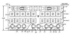
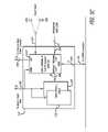
- FIG. 1Aa layout design of a flash dual inline memory module (DIMM) 100 A with flash memory 133 is illustrated.
- the flash memory 133in this case operates with a different voltage (voltage F) than the external power supply voltage (voltage E) furnished at the edge connector 102 .
- the flash DIMM 100 Aincludes on one or both sides of the printed circuit board 101 , a DIMM edge connector 102 , power supply conversion and regulation circuitry 104 , a plurality of memory support circuits (e.g., data support application specific integrated circuits (ASICs) 115 for data support and commercially available address support chips or proprietary address support application specific integrated circuits 117 ), and flash memory chips 133 coupled together by a plurality of printed circuit board traces, such as trace 160 for example between a pad 150 of the edge connector 102 and a pin of the data ASIC 115 .
- ASICsdata support application specific integrated circuits
- the memory module 100 Afurther includes a plurality of printed circuit board traces 160 (e.g., printed wires) formed on and/or in one or more layers of the PCB 101 to electrically couple the packaged parts together to each other and/or to the pads 150 of the edge connector 102 .
- the packaged parts, devices, and circuitsare mounted to the printed circuit board (PCB) they are mounted on a surface (e.g., a surface layer of printed circuit board traces) of the PCB on a front side, a back side, or both front and back sides as well as electrically coupled to the printed circuit board traces.
- a DIMM connector 102may have 240 pins or pads of which 72 bits may be used for data, 28 to 40 pins may be used for address/control, and the remaining pins or pads may be used for power and ground.
- the plurality of memory support chipsmay be used to buffer and/or register addresses, and/or multiplex and de-multiplex data to and from the flash memory chips 133 .
- the flash memory dual inline memory module (FMDIMM) 100 Ais a non-volatile type of memory module.
- the non-volatile type of memory modulemay include at least one NOR-gate flash electrically erasable programmable read only memory (EEPROM) integrated circuit.
- EEPROMelectrically erasable programmable read only memory
- NAND-gate flash electrically erasable programmable read only memory (EEPROM) integrated circuitsmay also be used in a flash memory DIMM.
- Phase shift dynamic random access memory (PSDRAM)may also be used in a flash memory DIMM.
- memory typesmay be mixed in a flash memory DIMM.
- non-volatile memorysuch as EEPROM flash memory may be mixed with volatile memory such as standard DRAM memory to form a flash memory DIMM.
- Non-volatile memory of any typemay also be generally referred to herein as flash memory.
- Flash memorymay operate using one power supply voltage (voltage F).
- Computer systemsmay operate at different power supply voltage (voltage E) such that the signals and power supply expected and provided at the DIMM edge connector when plugged in are in accordance with DIMM edge connector power and signal standards.
- the power supply conversion and regulation circuitry 104converts the external power supply voltage (voltage E) from the edge of the DIMM connector 102 into the operating power supply voltage (voltage F) for the flash memory 133 .
- the power supply voltages levels to be provided at the edge connectormay be in accordance with Joint Electron Device Engineering Council's (JEDEC) double data rate (DDR) memory standards (2.5 volts), JEDEC DDR2 memory standards (1.8 volts), or JEDEC DDR3 memory standards for dual inline memory modules (1.5 volts).
- JEDECJoint Electron Device Engineering Council's
- DDRdouble data rate
- the Joint Electron Device Engineering Councilis the semiconductor engineering standardization body of the Electronic Industries Alliance (EIA), a trade association representing many areas of the electronics industry.
- EIAElectronic Industries Alliance
- a power supply voltage of 1.8 voltsmay be provided and the circuitry 104 converts the 1.8 volts into a 3.3 volt power supply expected by some generations of flash memory 133 .
- a power supply voltage of 1.5 voltsmay be provided at the edge connector and the circuitry 104 converts the 1.5 volt power supply into a 1.8 volt power supply expected by another generation of flash memory 133 .
- Both of the power supplies with the different power supply voltagesmay be coupled into the address and data support ASICs 117 , 115 so that they can translate signals between each signaling standard.
- 1.8 volt standard signalsmay be expected while some generations of flash memory 133 may be expecting 3.3 volt standard signals at the chip interface.
- the address and data support ASICs 117 , 115may receive 1.8 volt standard signals for address/control and data from the edge connector and convert them into 3.3 volt standard signals for the flash memory.
- the address and data support ASICs 117 , 115may receive 3.3 volt standard signals for data from the flash memory and convert them into 1.8 volt standard signals for driving data out onto the edge connector.
- the address and data support ASICs 117 , 115may perform voltage translation for signals between the edge connector and the flash memory.
- the power supply conversion and regulation circuitry 104uses space on the printed circuit board (PCB) 101 as shown in FIG. 1A . Additionally, the address and data support ASICs and chips 117 , 115 take up space on the PCB 101 in a row along the connector 102 adding further to the height of the DIMM 100 as illustrated in FIG. 1A .
- PCBprinted circuit board
- the height added to the DIMM 100 A by power supply conversion and regulation circuitry 104 and the address and data support ASICs and chips 117 , 115may be so much that it exceeds one unit (1 U) standard height of thirty millimeters (mm). As a result of the larger height, the flash DIMM 100 A may not be usable in a number of computing systems that use one unit standard height DIMMs.
- the flash memory 133can be redesigned so that it can operate using the external voltage supplied at the DIMM edge connector instead so that the power supply conversion and regulation circuitry 104 may be eliminated from the DIMM 100 A. Moreover, the packaged flash memory 133 may only contain a single die.
- the flash memory coupled to the DIMMmay be re-packaged to include a plurality of flash memory die in one package to increase memory capacity and/or reduce the number of packaged parts mounted to the PCB of the DIMM. With fewer parts mounted to the PCB of the DIMM, the height of the DIMM may be reduced.
- the address and/or data support chips 117 , 115may be further packaged together with flash memory to reduce the height of a DIMM (e.g., a 16 giga-byte DIMM) down to thirty millimeter for one unit standard height systems.
- a DIMMe.g., a 16 giga-byte DIMM
- flash memory chips and address and data support ASICsmay also be used to reduce the number of PCB traces and further reduce the height of the PCB and DIMM. In this manner, a flash DIMM may be more widely sold and used to achieve economies of scale.
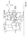
- FIG. 1Ba block diagram of a flash memory DIMM (FMDIMM) 100 B is illustrated.
- Several address/control buffer ASICsmay be integrated into a multi-chip package or multi-chip module (MCM) to form a multi-chip packaged address/control ASIC part 157 to reduce the height of the PCB.
- MCMmulti-chip package or multi-chip module
- a plurality of flash memory dice or die(e.g., four) may be mounted together into one multi-chip package or multi-chip module (MCM) to form a multi-chip packaged flash memory part 118 to reduce the height of the PCB.
- a support ASIC die and one or more flash memory dicemay be mounted together into one multi-chip package or multi-chip module (MCM) to form a multi-chip packaged flash memory/support ASIC part to further reduce the number of packaged parts mounted to the PCB of a FMDIMM.
- MCMmulti-chip package or multi-chip module
- hybrid packagean integrated circuit package with multiple chips mounted therein may have been referred to as a hybrid package or a multi-chip module. More recently, hybrid packages and multi-chip modules are referred to as multi-chip packages (MCP) or chip-scale packages (CSP), ignoring whether or not the chips are stacked upon each other or not.
- MCPmulti-chip packages
- CSPchip-scale packages
- the data support ASIC part 155multiplexes and de-multiplexes the data lines of the plurality of flash memory die with an external data bus.
- a four to one bus multiplexer and a one to four bus demultiplexeris provided by the data support ASIC part 155 .
- the flash memory DIMM 100 Bincludes a plurality of flash memory chips 118 with other memory support application integrated circuit (ASIC) chips that operate with a power supply that matches the expected signal levels and power supply of the computer system into which the FMDIMM 100 B may be plugged.
- ASICapplication integrated circuit
- the chipsuse a one and eight-tenths (1.8) volt power supply.
- the FMDIMM 100 Bis configured with two ranks (rank zero and rank one) of flash memory each having eighteen flash memory chips 118 with address lines 140 A, 140 B, 141 A, 141 B coupled into each flash memory chip 118 to address memory space.
- Rank zero and rank onemay each have nine flash memory chips 118 mounted onto the front of the PCB and nine flash memory chips 118 mounted onto the back side of the PCB for a total of thirty-six flash memory packages 118 being included as part of the FMDIMM 100 B.
- a plurality of flash memory integrated circuitsmay be packaged into one multi-chip package such as an MCM integrated circuit package to further reduce the number of packages mounted to the printed circuit board (PCB) of the FMDIMM.
- the flash memory DIMM 100 Bfurther includes address/control support ASIC parts 157 and data support ASIC parts 155 coupled together and to the flash memory parts 118 as illustrated.
- the data support ASIC parts 155may be mounted to the printed circuit board in a row next to the edge connector 102 .
- the address/control support ASIC parts 157may be mounted to the printed circuit board between a left plurality of flash memory parts 118 in each row and a right plurality of flash memory parts 118 in each row. There may be five memory slices 128 A- 128 E to one side of the address/control support parts 157 and four memory slices 128 F- 128 I to the other side of the address support parts 157 .
- the flash memory DIMM 100 Bmay have four address/control support ASIC parts 157 , two of which may be mounted on the front side and two of which may be mounted on the back side of the PCB.
- Two address/control support ASICs 157may be provided for each rank or row of flash memory.
- Each of the address/control support ASICs 157may receive address lines 145 that are used to register or latch address/control information over two clock cycles. Typically, the lower address bits are sent in the first clock cycle and the upper address bits/control bits are sent in the second clock cycle.
- a rank control signalmay be used to designate which rank of memory the address information is for.
- the address/control informationmay be decoded to generate address lines 140 A- 140 B for rank zero, address lines 141 A- 141 B for rank one, and multiplexer control signals 142 A- 142 B coupled to the data support ASIC parts 155 .
- the address lines 141 A- 141 B, 140 A- 140 B for memory ranks zero and onemay be routed between front and back sides of the PCB such as by means of through-holes, vias, or wrapping around an edge (e.g. bottom or top edge) of the PCB.
- Half of the address linesmay be generated by address support/control ASICs 157 on a front side of the PCB and the other half of address lines may be generated by address/control support ASICs 157 on the back side of the PCB.
- the address/control support ASICs 157may buffer and broadcast the addresses to the flash memory parts 118 to reduce loading of the address lines at the edge connector.
- Each sidemay have nine memory slices or columns 128 A- 128 I with each memory slice 128 including a flash memory chip 118 in rank one, a flash memory chip 118 in rank zero, and a data support ASIC 155 coupled together as shown in FIG. 1B .
- Each of the data support ASICs 155may include a four to one multiplexer and one into four demultiplexer so that bidirectional data can be communicated between a sixteen bit data bus 138 in each slice and a four bit data bus 139 into the connector 102 . That is, sixteen bits of data in bus 138 may be multiplexed out to four bits of the data bus 139 over four consecutive cycles when reading out data from the FMDIMM 100 B. When writing data into the FMDIMM 100 B, four bits of data on the data bus 139 from each of four consecutive data cycles may be de-multiplexed into four of the sixteen bits of the data bus 138 .
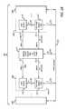
- FIG. 2Ais a functional block diagram of another configuration of a flash memory dual inline memory module (FMDIMM) 200 .
- the flash memory dual inline memory module (FMDIMM) 200includes a plurality of multi-chip packaged flash memory parts 118 , a plurality of multi-chip packaged flash memory/data support ASIC parts 210 , and a plurality of plurality of address support ASICs 157 coupled together as shown.
- the data support ASIC dieis of a relatively small die size so that it can be integrated with a flash memory chip into a multi-chip package 210 .
- the multi-chip packaged flash memory/data support ASIC part 210 including flash memorymay be used in one rank of memory, rank zero for example. This removes a number of the data support ASIC packages from the printed circuit board so that its height may be reduced.
- a plurality of address support ASICs 157may still be employed in the FMDIMM 200 so that the address pins/pads of the connector 102 are routed to both ranks (rank one and rank zero) independently, such that extra printed circuit board layers may be used to route the traces over other address lines.
- the FMDIMM 200includes a plurality of memory slices 228 A- 228 I (generally referred to as memory slice 228 ) on each side.
- Each memory slice 228includes one packaged flash memory chip 118 and one multi-chip packaged flash memory/data support ASIC packaged part 210 .
- the data on bus 139may be routed through the multi-chip packaged flash memory/data support ASIC part 210 to and from the flash memory chip 118 over the bus 138 .
- FIG. 2Bis a functional block diagram of the multi-chip packaged flash memory/data support ASIC part 210 of FIG. 2A .
- the multi-chip packaged flash memory/data support ASIC part 210includes one or more unpackaged flash memory dice 118 ′ and an unpackaged data support ASIC die 155 ′ coupled together as shown.
- the unpackaged flash memory and the unpackaged data support ASIC diceare mounted to a substrate of the multi-chip packaged with traces of the bus 138 routed between each.
- the four bit bus 139is coupled into the data support ASIC chip 155 ′.
- eighteen multi-chip packaged flash memory/data support ASIC parts 210 in a rankeighteen data support ASIC dice 155 ′ are used per FMDIMM 200 .
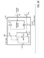
- the flash memory DIMM 300includes a plurality of multi-chip packaged flash memory/support ASIC parts 310 A- 310 B (collectively referred to by the reference number 310 ) and standard DDR2 address registers 301 - 302 coupled together.
- a portion of the address/control support ASIC 157is combined with the data support ASIC 155 into one die and mounted with flash memory dice into a multi-chip package (MCP) to form the multi-chip packaged flash memory/support ASIC part 310 .
- MCPmulti-chip package
- the number of address linesmay be reduced and the number of PCB board layers may be reduced to lower cost of manufacturing the FMDIMM.
- the multi-chip packaged flash memory/support ASIC part 310provides data, address, and control support, it may also be referred to as a multi-chip packaged flash memory/address, control, & data support ASIC part 310 .
- the FMDIMM 300includes a plurality of memory slices 328 A- 328 I on each side. Each memory slice 328 includes a pair of multi-chip packaged flash memory/support ASIC parts 310 A- 310 B.
- the data on bus 139may be routed through the multi-chip packaged flash memory/support ASIC part 310 A to and from the multi-chip packaged flash memory/support ASIC part 310 B over the bus 138 .
- the multi-chip packaged flash memory/support ASIC part 310 Bmay be substantially similar to the multi-chip packaged flash memory/support ASIC part 310 A. However, the multi-chip packaged flash memory/support ASIC packaged part 310 B is not directly coupled to the connector 102 of the DIMM 300 so it may be simplified and with data being passed to it, it may operate somewhat differently.
- the multi-chip packaged flash memory/support ASIC packaged part 310 Apasses data from the edge connector 102 through it to the multi-chip packaged flash memory/support ASIC packaged part 310 B over the bus 138 .
- the multi-chip packaged flash memory/support ASIC packaged part 310 Amay receive data from the multi-chip packaged flash memory/support ASIC packaged part 310 B on the bus 138 and pass it through it to the edge connector 102 .
- the address lines 145 from the edge connector 102are coupled into the address register 302 .
- the addressmay be passed from the address register 302 to the address register 301 over the address bus 345 .
- Each of the address registersdrives address lines out each side.
- the address register 301drives address lines 340 A to the slices 328 A- 328 E and address lines 340 B to the slices 328 F- 328 I.
- the address register 302drives address lines 341 A to the slices 328 A- 328 E and address lines 341 B to the slices 328 F- 328 I.
- the number of address linesis reduced because the addresses are buffered and fully formed in the support ASIC residing in the packages 310 A- 310 B reducing the routing traces and the space used on the PCB.
- the multi-chip integrated circuit packageshave fewer pins which may reduce packaging costs.
- the address bus widthis cut in half by sending the complete address over 2 cycles reducing the number of address traces on the PCB, the number of PCB board layers may be reduced as a result.
- FIG. 3Bis a functional block diagram of the multi-chip packaged flash memory/support ASIC part 310 A of FIG. 3A .
- the multi-chip packaged flash memory/support ASIC part 310 Aincludes one or more unpackaged flash memory dice 118 ′ and an unpackaged address/control/data support ASIC die 350 coupled together as shown.
- the chipsare mounted to a substrate of the multi-chip package with traces of the data bus 138 and the flash address bus 348 routed between each as illustrated.
- the bit data bus bits 139 and the input address bus 341are coupled to the address/control/data support ASIC chip 350 .
- the address/control/data support ASIC 157may be integrated with the function of the data support ASIC 155 into one chip, the address/control/data support ASIC chip 350 .
- the address/control/data support ASIC chip 350requires the use of more input/output pins.
- the data latency into and out of the FMDIMMmay be increased by one clock cycle.
- the flash memory DIMM 400includes a plurality of multi-chip packaged flash memory/support ASIC parts 410 and address registers 301 - 302 coupled together.
- the multi-chip packaged flash memory/support ASIC part 410provides data, address, and control support, it may also be referred to as a multi-chip packaged flash memory/address, control, & data support ASIC part 410 .
- the FMDIMM 400includes a plurality of memory slices 428 A- 428 I on each side. In one implementation, nine memory slices 428 A- 428 I on each side are divided by the address registers 301 - 302 into five and four memory slices into a row. Each memory slice 428 includes a pair of multi-chip packaged flash memory/support ASIC packaged parts 410 .
- the data bus 139is coupled to each of the multi-chip packaged flash memory/support ASIC packaged parts 410 so that a pass through bus 138 is not needed, thereby reducing the number of routing traces on the printed circuit board.
- the FMDIMM 400has a data bus shared between memory ranks zero and one. With the number of lines of an address bus cut in half and the number of lines of a data bus significantly reduced, the number of layers in the PCB may be reduced as well.
- the address register 301drives 20 address lines 340 A to the slices 428 A- 428 E and 20 address lines 340 B to the slices 428 A- 428 I coupling to the upper row multi-chip packaged flash memory/support ASIC packaged parts 410 in each.
- the address register 302drives 20 address lines 341 A to the slices 428 A- 428 E and 20 address lines 341 B to the slices 428 F- 428 I coupling to the lower row multi-chip packaged flash memory/support ASIC packaged parts 410 in each.
- FIG. 4Bis a functional block diagram of the multi-chip flash memory/support ASIC packaged part 410 of FIG. 4A .
- the multi-chip packaged flash memory/support ASIC part 410includes one or more unpackaged flash memory dice 118 ′ and an unpackaged address/control/data support ASIC die 450 coupled together as shown.
- the diceare mounted to a substrate of the multi-chip packaged package with traces of the data bus 438 and an address bus 348 routed between each as illustrated.
- the four bit data bus 139 and the address bus 341are coupled to the address/control/data support ASIC die 450 .
- a portion of the function of the address/control support ASIC 157may be integrated with the function of the data support ASIC 155 into one die, the address/control/data support ASIC die 450 .
- the extra functionality, the address/control/data support ASIC die 450may use additional input/output pins.
- the address/control/data support ASIC die 450is functionally more complex with more gates and thus has a larger die size and may cost more to manufacture. If the address/control/data support ASIC die 450 is implemented as a programmable logic device, it is a complex programmable logic device (CPLD). For thirty-six multi-chip packaged parts 410 in each FMDIMM, there may be a total of thirty six address/control/data support ASIC dice on a PCB, one in each package.
- CPLDcomplex programmable logic device
- the multi-chip packaged flash memory/support ASIC part 410may have fewer pins that the MCP flash memory/support ASIC part 310 A as the pass through bus 138 need not be supported by it. Instead, the data bus 438 is internal within the multi-chip packaged flash memory/support ASIC part 410 . With fewer pins, the multi-chip packaged flash memory/support ASIC part 410 may cost less.
- the FMDIMM 300may apply less parasitic load onto the edge connector 102 than the FMDIMM 400 . However without the shared wider data bus, there is less routing traces on the printed circuit board as the data bus 138 is not used to pass data between parts in a slice.
- FIGS. 5A-5Drespectively represent a functional block diagram of a front side 500 F and a back side 500 B of another implementation of a FMDIMM 500 .
- the front side 500 F of the FMDIMM 500includes multi-chip packaged flash memory parts 518 F, and 518 B, and multi-chip packaged flash memory/support ASIC parts 510 F, and an address register 301 F coupled together as shown.
- the address register 301 Fis an off-the-shelf or standard DDR2 memory address register.
- the multi-chip packaged flash memory/support ASIC part 510 Fprovides data, address, and control support, it may also be referred to as a multi-chip packaged flash memory/address, control, & data support ASIC part 510 F.
- the FMDIMM 500includes a plurality of memory slices 528 A- 528 I on one side and a plurality of memory slices 528 I′- 528 A′ on the other side of the FMDIMM 500 .
- a front side address register 301 Fmay be connected to the nine front side packages 510 F through the traces 540 A- 540 B.
- a back side address register 301 Bmay be connected to the nine back side packages 510 B through the traces 540 A′- 540 B′.
- Each front side memory slice 528includes a multi-chip packaged flash memory part 518 F and a multi-chip packaged flash memory/support ASIC part 510 F coupled together as shown by a pass through data bus 538 F and a pass through address/control bus 548 F.
- the front side address/control bus 548 F in each sliceis also routed through vias 568 to the back side of the FMDIMM 500 connecting to a multi-chip packaged flash memory part 518 B on the back side.
- a back side address/control bus 548 Bmay be routed from the back side to the front side of the FMDIMM 500 such as through vias or feed-throughs (or alternatively by wrapping around an edge of the PCB) and is coupled into the front side flash memory part 518 F.
- Front side data bus bits 139 Fa subset of the respective data bits of the edge connector 102 , are coupled to each of the multi-chip packaged flash memory/support ASIC parts 510 F in each memory slice 528 A- 528 I on the front side.
- Each memory slicecouples to a respective subset of the total data bits at the edge connector of the DIMM. This may reduce the number of data bus signals routed over each side of the chip to reduce the size of the PCB, reduce the number of layers in the PCB, and/or reduce the loading on the edge connector 102 . With the number of address lines routed across the FMDIMM being reduced as well, the size of the PCB and the number of layers in the PCB may be further reduced.
- the front side address register 301 Freceives address lines from the connector 102 and registers an address or control signals that may be multiplexed on the address lines.
- the address register 301 Fcan then drive out the address or control signals on the address/control lines 540 A to the slices 528 A- 528 E and address/control lines 540 B to the slices 528 F- 528 I coupling to the multi-chip packaged flash memory/support ASIC packaged parts 510 F in each.
- a front/back signal line 541 Ais coupled into the slices 528 A- 528 E and a front/back signal line 541 B to the slices 528 F- 528 I coupling to the hybrid flash memory/ASIC packaged parts 510 F in each.
- the front/back signal line 541 Ais tied to power (VDD) or to ground (VSS) in the package or externally.
- the front/back signal line 541 Atells the memory support ASIC if it is to operate in a front mode or a back mode.
- the front/back signal line 541 A signalwill be used by the memory support ASIC to send upper or lower address bits to flash memory part 518 F above it in the memory slice 528 .
- the front/back signal linetells the ASIC 510 F to send the upper 16 or lower 16 address bits to the flash memory packages 518 in the top rank.
- the front/back signal lines 541 A- 541 Bare tied to power VDD for the front side flash memory 518 F and the front side hybrid part 510 F to operate in a front side mode on the FMDIMM 500 .
- FIG. 5Billustrates a back side 500 B of the PCB and the flash memory DIMM 500 mirroring the front side of the FMDIMM 500 so that the PCB traces are further reduced to minimize the size of the printed circuit board.
- the back side of the flash memory DIMM 500includes back side flash memory parts 518 B, hybrid flash memory/ASIC parts 510 B, and an address register 301 B coupled together as shown.
- the address register 301 Bis an off-the-shelf or standard DDR2 memory address register.
- the back side memory slice 528 A′ on the rightis parallel to the front side memory slice 528 A.
- the back side memory slice 528 I′ on the leftis parallel to the front size memory slice 528 I.
- the flash memory parts 518 F- 518 Bmay be mounted substantially in parallel to each other on opposite sides of the PCB.
- the hybrid parts 510 F and 510 Bmay be mounted substantially in parallel to each other and the flash memory parts 518 F and 518 B on opposite sides of the PCB to minimize the length and number of PCB routing traces.
- the front side address/control bus 548 Fis also routed through vias 568 to the back side of the FMDIMM 500 and coupled into the backside flash memory parts 518 B.
- the back side address/control bus 548 B generated by the back side hybrid flash memory/memory support ASIC part 510 Bis coupled into the back side flash memory part 518 B and routed from the back side to the front side of the FMDIMM to couple into the front side flash memory part 518 F.
- a four bit data bus 139 B of a respective four data bits of the connector 102is coupled to the hybrid flash memory/ASIC packaged part 510 B.
- address lines routed across the FMDIMMbeing further reduced, the size of the PCB and the number of layers in the PCB may be reduced.
- the address register 301 Breceives 20 address lines from the connector 102 and registers the address to then drive 20 address lines 540 A′ to the slices 528 F′- 528 I′ and 20 address lines 540 B′ to the slices 528 A′- 528 E′ coupling to the hybrid flash memory/ASIC packaged parts 510 B in each.
- the address register and data support ASICmay be combined into one address and data support ASIC 510 ′ in one implementation to further reduce the number of packages on the PCB (see FIG. 5D ).
- a front/back signal line 541 A′is coupled into the slices 528 A′- 528 E′ and a front/back signal line 541 B′ to the slices 528 F′- 528 I′ coupling to the hybrid flash memory/ASIC packaged parts 510 B in each.
- the front/back signal lines 541 A′- 541 B′are similar to the front/back signal lines 541 A- 541 B previously described. However in one configuration, the front/back signal lines 541 A′- 541 B′ are tied to ground VSS as illustrated for the back side flash memory 518 B and the back side hybrid part 510 B to operate in a back side mode on the FMDIMM 500 .
- the back side flash memory parts 518 B, MCP flash memory/support ASIC parts 510 B, and the address register 301 Bare mirror images of their front side counter parts 518 F, 510 F, 301 F to reduce conductive traces on a printed circuit board of the memory module and the number of layers needed. That is, the pinouts are mirror images. A mirror imaged pinout may be accomplished in a number of ways.
- the package for the flash memory part 518 Bmay be constructed to use the same dice as used in the front flash memory part 518 F, but the package for the back side flash memory part 518 B may be internally wired differently to mount to the backside of the memory module and mirror the front side flash memory part 518 F on a front side of the memory module.
- the integrated circuit die for the back sidemay be altered from the front side die. That is, the pinout of the flash memory die for the back side parts 518 B may be altered to mirror the pinout of the front side flash memory parts 518 F.
- the layouts of the back side flash memory partsdiffer physically from the layouts of the front side flash memory parts to mirror the pinout.
- a front/back control signalmay be tied logically high or low and used to electronically alter the pinout configuration to provide a mirrored pinout.
- the packages for the flash memory parts 518 F and 518 Bhave been described as having mirrored pinouts in different implementations, the multi-chip packaged flash memory/support ASIC parts 510 F, 510 B and the address register parts 301 F, 301 B may be similarly implemented to provide mirrored pinouts for the respective front and back sides of the FMDIMM 500 .
- a front/back control signal 541 A, 541 B and 541 A′, 541 B′may be used to electronically alter the pinout configuration of multi-chip packaged flash memory/support ASIC parts 510 F, 510 B to provide a mirrored pinout.
- the chipselectronically alter their pinout configurations by rerouting signal lines to different input/output pads on the chip.
- the front/back control signal 541 A, 541 Bmay be tied logically high to VDD routing the signals into a first routing pattern to provide a front side pinout for the multi-chip packaged flash memory/support ASIC parts 510 F mounted to the front of the DIMM.
- the front/back control signal 541 A′, 541 B′may be tied logically low to VSS routing the signals into a second routing pattern to provide a mirroring back side pinout for the multi-chip packaged flash memory/support ASIC parts 510 B mounted to the back side of the DIMM.
- the multi-chip packaged flash memory/support ASIC part 510includes one or more unpackaged flash memory dice 118 ′ and an unpackaged address/control/data support ASIC die 550 coupled together as shown.
- the chipsare mounted to a substrate of the multi-chip package with traces of the data bus 538 and the address bus 348 routed between each as illustrated.
- a plurality of data bus bits 139 and a plurality of address bus bits 341are coupled to the address/control/data support ASIC die 550 .
- the address/control buses 548 F and 548 B to Rank 1are shared between the front and back Rank zero flash memory packages 518 so each package only outputs one multiplexed address/control bus to reduce the pin count.
- the address/control/data support ASIC die 550has an address/control bus 548 that is shared with the flash memory chip 518 in each respective memory slice for addressing the top rank (rank one) of flash memory 518 .
- the data bus 538is extended out of the multi-chip package to be shared with the flash memory chip 518 in each respective memory slice as well.
- a front/back signal line 541is coupled into ASIC die 541 .
- the front/back signal line 541is tied to power (VDD) or to ground (VSS) in the package 510 or externally.
- the front/back signal line 541tells the memory support ASIC 550 if it is to operate in a front mode or a back mode.
- the front/back signal line 541 signalwill be used by the memory support ASIC to send upper or lower address bits to the flash memory part 518 above it in the memory slice 528 .
- the front/back signal linetells the ASIC 550 to send the upper 16 or lower 16 address bits on the bus 548 to the flash memory packages 518 in the top rank.
- the address/control/data support ASIC chip 550may be integrated with the function of the data support ASIC 155 into one chip, the address/control/data support ASIC chip 550 .
- the address/control/data support ASIC chip 550requires extra input/output pins.
- the address/control/data support ASIC chip 550is functionally more complex with more gates and thus has a large die size and a greater cost. If implemented as a programmable logic device, it is a complex programmable logic device (CPLD). For two ranks with eighteen multi-chip packaged flash memory/support ASIC parts 510 in the bottom rank, there are a total of eighteen CPLD ASICs for one FMDIMM 500 .
- CPLDcomplex programmable logic device
- the data latency into and out of the FMDIMMmay be increased by one clock cycle.
- the memory support ASIC 550is integrated a multi-chip package such as a multi-chip module (MCM) integrated circuit package.
- MCMmulti-chip module
- the FMDIMM 500may use one standard off the shelf DDR2 address register part 301 for both ranks of memory. As the buses 538 and 548 can be readily routed between parts in each slice, it may be easy to route conductors between all of the parts mounted onto the PCB of the FMDIMM 500 . This may result in area or space savings on the PCB to further reduce the size. Moreover, the flash memory 518 for the top rank, (rank one), may be packaged in a standard multi-chip module integrated circuit package. The package part 510 has extra pins added to its package to provide the pass-through of data, address, and controls to the flash memory part 518 .
- FIG. 5Da functional block diagram of the multi-chip packaged flash memory/support ASIC part 510 ′ is illustrated.
- the multi-chip packaged flash memory/support ASIC part 510 ′is similar to the multi-chip packaged flash memory/support ASIC part 510 .
- the multi-chip packaged flash memory/support ASIC part 510 ′includes an integrated address register 301 to avoid the separate packaged address registers 301 F and 301 B in one implementation to further reduce the number of packages mounted on the PCB.
- the ASIC die 550 ′receives the address bits 145 from the connector 120 and couples them into the address register 301 .
- the ASIC die 550 ′buffers the address signals and drives them out onto the address lines 540 A and 540 B to the other multi-chip packaged flash memory/support ASIC parts 510 in the row.
- the number of multi-chip packaged flash memory/support ASIC parts 510 mounted on the DIMMmay be reduced. For two ranks with only nine multi-chip packaged flash memory/support ASIC parts in the bottom rank, there are a total of nine CPLD ASICs for one FMDIMM.
- the flash memory partincludes one or more unpackaged flash memory die 118 ′ (e.g., a monolithic semiconductor substrate) mounted to a package substrate 601 of an integrated circuit package 600 .
- the integrated circuit package 600is a standard multi-chip module integrated circuit package.
- Address and/or control lines 141 , 548 F, 548 Bare coupled to the one or more unpackaged flash memory dice 118 ′.
- Data lines 138 , 538are also coupled to the one or more unpackaged flash memory dice 118 ′.
- FIGS. 8A and 8Brepresent a functional block diagram of a front side 800 A and a back side 800 B of an FMDIMM 800 is illustrated.
- the FMDIMM 800includes multi-chip packaged flash memory parts 818 F and 818 B respectively on front and back side, multi-chip packaged flash memory/support ASIC parts 810 F on the front side, and an address register 301 on the front side coupled together as shown.
- the address register 301 Fis an off-the-shelf or standard DDR2 memory address register.
- the multi-chip packaged flash memory/support ASIC part 810 Fprovides data, address, and control support, it may also be referred to as a multi-chip packaged flash memory/address, control, & data support ASIC part 810 F.
- the FMDIMM 800includes a plurality of memory slices 828 A- 828 I on one side (e.g., front side 800 F) and a plurality of memory slices 828 I′- 828 A′ on the other side (e.g., back side 800 B) of the FMDIMM 800 .
- the address register 301 Fis connected to the nine multi-chip packaged flash memory/support ASIC part 810 F on via traces 840 .
- Each front side memory slice 828includes a multi-chip packaged flash memory part 818 F and a multi-chip packaged flash memory/support ASIC part 810 F coupled together as shown by a pass through address low/data bus 838 and a pass through address high/control bus 848 .
- the address high/control bus 848is also routed through vias or feed-throughs 868 to the back side of the FMDIMM 800 connecting to the multi-chip packaged flash memory parts 818 B mounted on the back side 800 B in each respective slice.
- the address low/data bus 838is also routed through vias or feed-throughs 869 to the back side of the FMDIMM 800 connecting to the multi-chip packaged flash memory parts 818 B mounted on the back side 800 B in each respective slice.
- Data bus bits 139 F of respective data bits of the connector 102are coupled to the multi-chip packaged flash memory/support ASIC part 810 F.
- the address register 301 Freceives address lines from the connector 102 and registers the address to then drives address lines 840 A to the slices 828 A- 828 I coupling to the hybrid flash memory/support ASIC packaged parts 810 F in each. With address lines routed across the FMDIMM being further reduced, the size of the PCB and the number of layers in the PCB may be reduced
- FIG. 8Billustrates a back side 800 B of the PCB and the flash memory DIMM 800 .
- the back side of the flash memory DIMM 800includes back side flash memory parts 818 B in each respective memory slice 828 I′- 828 A′ as shown.
- the memory slices 828 I′- 828 A′ on the back sidemirror the memory slices 828 A- 828 I on the front side so that the PCB traces to minimize the size of the printed circuit board.
- the back side memory slice 828 A′ on the rightis behind the front side memory slice 828 A.
- the back side memory slice 828 I′ on the leftis behind the front size memory slice 828 I.
- the flash memory parts 818 F and 818 Bmay be mounted substantially in parallel to each other on opposite sides of the PCB.
- the MCP flash memory/support ASIC parts 810 Fmay be mounted substantially in parallel to flash memory parts 818 B on opposite sides of the PCB to minimize the length and number of PCB routing traces.
- the address high/control bus 848 and the address low/data bus 838are routed from the front side to the back side through the vias or feedthroughs 868 and 869 respectively.
- portions of the address high/control bus 848 and the address low/data bus 838are coupled into the two rows of backside flash memory parts 818 B.
- back side flash memory parts 818 Bsuch as address/high control pins, may have signal assignments which mirror images of their front side counter parts to reduce conductive traces on a printed circuit board of the memory module and the number of layers needed. That is, one or more of the pin outs of the back side flash memory parts 818 B are mirror images of the front side flash memory parts 818 F.
- Various ways of implementing mirror imaged pinoutswere previously described and are incorporated here by reference.
- the multi-chip packaged part 810includes one or more unpackaged flash memory dice 118 ′ and an unpackaged address/control/data support ASIC die 850 coupled together as shown.
- the chipsare mounted to a substrate of the multi-chip package with traces of the address low/data bus 838 and address high/control bus 848 , 848 I routed between each as illustrated.
- Data bus bits 139 and a multiplexed address/control bus 840are coupled into the address/control/data support ASIC die 850 .
- the support ASIC 850drives out the higher address bits and control bits directly to the flash memory die(s) over internal signal lines 848 I while driving out higher address bits and control bits for the other front side flash memory packages 818 F and the back side flash memory packages 818 B on bus 848 .
- the row of components on the front and back sides closest to the edge connector 102may be referred to as memory rank zero.
- the upper row of components on the front and back sides furthest away from the edge connector 102may be referred to as memory rank one.
- the subset of the bits of the address/control bus 848 which pertain to memory rank zeroare shared between the front and back memory rank zero flash memory in the multi-chip packages 810 and 818 B so that each package connects to one address/control bus to reduce the printed circuit board trace count.
- a subset of the address/control bus which connects to rank oneis respectively shared between the front and back rank one flash memory parts 818 F and 818 B.
- the address/control/data support ASIC die 850has an address/control bus 848 that is shared with the flash memory chip 818 F on the front side and the flash memory packages 818 B on the back side in each respective memory slice.
- the address low/data bus 838is extended out of the multi-chip packaged integrated circuit package to be shared with the flash memory in the multi-chip packages 810 and 818 F on the front side connecting to half the bus 838 and the multi-chip flash memory packages 818 B on the back side connecting to the other half of the bus 838 in each respective memory slice as well.
- the address/control/data support ASIC chip 850may be integrated with the function of the data support ASIC 155 into one chip, the address/control/data support ASIC chip 850 .
- the address/control/data support ASIC chip 850requires extra input/output pins.
- the address/control/data support ASIC chip 850may be functionally more complex with more gates and thus may have a large die size and be manufactured at greater cost. If implemented as a programmable logic device, it is a complex programmable logic device (CPLD). For two ranks with nine MCP flash memory/support ASIC parts 810 in the bottom rank, there are a total of nine CPLD ASICs for one FMDIMM 800 .
- CPLDcomplex programmable logic device
- the data latency into and out of the FMDIMMmay be increased by one or more clock cycles.
- the FMDIMM 800may use one standard off the shelf DDR2 address register part 301 for both ranks of memory. As the address register part 301 connects to the front support ASIC parts 810 , and as buses 838 and 848 are routed between parts in each slice, there may be area or space savings on the PCB to further reduce its size. Moreover, the flash memory parts 818 F on the front side and the flash memory parts 818 B on the back side may be packaged in a multi-chip package. The multi-chip packaged flash memory/support ASIC part 810 has extra pins added to its package to provide data pass-through of data signals, address pass-through of address signals, and control pass-through of control signals to the flash memory parts 818 F, 818 B.
- the flash memory part 818includes one or more unpackaged flash memory die(s) 118 ′ (e.g., a monolithic semiconductor substrate) mounted to a package substrate 801 of an integrated circuit package 800 .
- the flash memory dicemay be NOR-gate flash electrically erasable programmable read only memory (EEPROM) integrated circuit in some implementations.
- the integrated circuit package 800may be a multi-chip module integrated circuit package.
- Selected address/control lines of the address high/control bus 848are coupled into the one or more unpackaged flash memory dice 118 ′ depending upon the mounting (front or back) of the part 818 and the rank of memory (e.g., rank one or zero) it is to operate on the DIMM.
- Selected address/data lines of the address low/data bus 838are also coupled into the one or more unpackaged flash memory dice 118 ′ depending upon the mounting (front or back) of the part 818 and the rank of memory (e.g., rank one or zero) it is to operate on the DIMM.
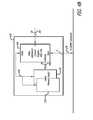
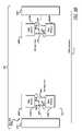
- the flash memory support ASIC die 900may provide data, address, and control support for the flash memory on a DIMM.
- the flash memory support ASIC die 900includes an address/control block 902 , a data path buffer 904 , a data multiplexer/de-multiplexer 906 , and clock/status block 908 coupled together as shown.
- the address/control block 902is coupled to the address/control bus 913 to receive input addresses and control signals that may be multiplexed thereon.
- the address/control block 902may further be coupled to control signal lines 914 to further receive clock signals to synchronize address and data and generate control signals at the appropriate moments.
- the address/control block 902In response to the input signals 913 and 914 , the address/control block 902 generates control signals 924 coupled to the data path buffer 904 to store data into and/or write data out there-from.
- the address/control block 902further generates control signals 922 coupled to the multiplexer/de-multiplexer 906 and the data path buffer 904 to synchronously control their functional operations.
- the address/control block 902further generates addresses and control signals onto a pair of external address high/control buses 912 A- 912 B for memory ranks zero and one, as well as address signals on the internal address bus 923 to couple them into the multiplexer/de-multiplexer 906 for multiplexing onto the external address low/data bus 911 as required.
- flash memory integrated circuitssuch as NOR FLASH EEPROM integrated circuits
- read access timeswhere an address is presented and data returned
- read and write operations to flash memorymay be asymmetric.
- a data write operation into flash memorymay take much more time than a data read operation from flash memory.
- a data erase operation in flash memorymay also take much more time than a data read operation.
- the data path buffer 904may be used to store data so that the asymmetry in read and write operations with flash memory may be emolliated. Data may be quickly written into the data path buffer 904 and then controlled to program large amounts of data into the flash memory at another moment in time. Similarly, a plurality of data read operations into flash memory may be made with data being stored into the data path buffer 904 . The data may be read out in bursts from the data path buffer. Additionally, signal timing differences between a data bus to the flash memory die and an external data bus to the edge connector of a DIMM may be emolliated by the buffering provided by the data path buffer 904 .
- the data bus 911 coupled to flash memory dice and consequently internal data bus 921may have data clocked in/out every twenty nano-seconds (ns) while the data bus 916 coupled to the edge connector may have data clocked in and out data every five nano-seconds.
- the buffering provided by the data path buffer 904can smoother over these timing differences so they are transparent to each of the flash memory dice coupled to bus 911 and the devices coupled to bus 916 through the edge connector.
- the data path buffer 904is a data buffer includes memory, registers or other data storage means for each data bus 916 and 921 coupled to it to provide the buffering.
- the parallel bits (e.g., eight) of the data bus 916 coupled into the data path buffer 904may be less than the parallel bits (e.g., thirty-two) of internal data bus 921 coupled to the multiplexer/de-multiplexer 906 .
- the data path buffer 904facilitates packing data into wider bit widths for storage into one or more flash memory parts and unpacking the wide data bytes read out from one or more flash memory parts into narrower data bytes for reading over a fewer number of bits of the external memory input/output data bus 916 .
- the multiplexer/de-multiplexer 906is coupled to the data buffer 904 over the internal data bus 921 and the address and control block 902 over the internal address bus 923 .
- the multiplexer/de-multiplexer 906further receives control signals 922 from the address and control block 902 to control its multiplexing/demultiplexing functions.
- the multiplexer/de-multiplexer 906is further coupled to the multiplexed address low/data bus 911 that is coupled to flash memory dice.
- the multiplexer/de-multiplexer 906includes a many-to-one bus multiplexer and a one-to-many bus de-multiplexer jointly functioning similar to a cross-bar switch.
- a cross-bar switchmay be alternatively used to implement the functions of the many-to-one bus multiplexer and the one-to-many bus de-multiplexer.
- the many-to-one bus multiplexerallows a large amount of data to be read accessed in parallel, and then transferred out through the data path buffer 904 over a narrower data bus in a burst of cycles.
- the one-to-many bus demultiplexer in conjunction with the data path buffer 904may be used over a burst of cycles to receive parallel data of a narrower width from the external data bus and to write out the aggregated data out to the flash memory die.
- the bus multiplexing provided by the multiplexer/de-multiplexer 906allows extra flash memory dice to be stacked up behind the ASIC support chip on each side of the DIMM so that is has a greater memory capacity available than otherwise possible without the support chips.
- the use of the memory support ASIC chipavoids adding extra capacitive loading onto a memory channel bus from the extra flash memory dice in the memory module.
- the clock/status block 908is coupled to the data path buffer 904 to receive control signals and status information 925 regarding data being written out from the support ASIC 900 onto the external memory data input/output bus 916 .
- the clock/status block 908further receives input control signals 919 .
- the clock/status block 908may generate clock signals 918 to couple to the flash memory dice to synchronize the signal timing on the buses 911 and 912 A- 912 B coupled to the flash memory dice.
- the clock/status block 908further generates data synchronization clocks and a ready/busy signal(s) 917 to be provided over the edge connector to synchronize the signal timing on the data bus 916 for data driven out from the data path buffer 904 .
- the ready/busy signal(s) of the control signals 917is a status signal and provides status of a requested operation with the flash memory.
- the ready/busy signalmay be generated by the clock/status block 908 of the support ASIC 900 so that so that the flash memory dice may be more efficiently accessed.
- the status signalmay indicate whether or not the flash memory coupled to the support ASIC is busy or ready for another write or erase access to alleviate the non-deterministic nature of erase and write operations to flash memory.
- the control input signals 919may be used to determine what information a support ASIC die reports in the clock/status block 908 .
- the memory support ASICis integrated with flash memory into a multi-chip package (MCP).
- MCPmulti-chip package
- FIG. 7Aa side cutaway view of a multi-chip packaged flash memory/support ASIC part 700 A is illustrated.
- multi-chip packagesmay have been referred to as hybrid packages or multi-chip module packages.
- Mounted in the package 701 Ais a top flash memory die 118 ′, a combined spacer/memory support ASIC die 702 , and a lower flash memory die 118 ′.
- the spacer/memory support ASIC die 702includes a spacer 712 in a middle portion and active devices 704 A- 704 B near outer portions beyond the dimensions of the top and bottom flash memory die 118 ′.
- the spacer 712may be a dielectric or insulator so that the active devices 704 A- 704 B of the spacer/memory support ASIC die 702 do not short to any circuitry of the flash memory die 118 ′. Otherwise, the middle portion does not include any active devices or metal routing near its surfaces so that it can act as a non-shorting spacer to the top and bottom flash memory die.
- Metal routing or interconnectmay be buried and insulated in the spacer 712 in the middle portion of spacer/memory support ASIC die 702 to couple active devices 704 A- 704 B in the outer portions together.
- Conductors 705 A- 705 Bmay couple the top flash memory die 118 ′ to the active portions 704 A- 704 B of the memory support ASIC die 702 .
- Conductors 706 A- 706 Bmay couple the bottom flash memory die 118 ′ to the active portions 704 A- 704 B of the combined spacer/memory support ASIC die 702 .
- Conductors 714 A- 714 Bmay couple the combined spacer/memory support ASIC die 702 to pin-out connections 750 .
- Conductors 715 - 716may respectively couple the top and bottom flash memory die 118 ′ to the pin-out connections 750 .
- An encapsulant 721may be used to protect the devices mounted in the package 701 A and keep conductors from shorting to each other.
- FIG. 7Ba side cutaway view of a multi-chip packaged flash memory/support ASIC part 700 B is illustrated.
- a memory support ASIC die 703Mounted in the multi-chip module package 701 B is a memory support ASIC die 703 , and pairs of a spacer and a flash memory die including a first spacer 722 A and a first flash memory die 118 ′, a second spacer 722 B and a second flash memory die 118 ′, a third spacer 722 C and a third flash memory die 118 ′, and an Nth spacer 722 N and an Nth flash memory die 118 ′ stacked together as shown.
- the spacer 722 Amay be the size of the support ASIC 703 as shown or somewhat smaller than the size of the flash memory 118 ′ so that contacts may be made to the support ASIC die 703 and the first flash memory die 118 ′.
- the flash memory die 118 ′is larger than the spacers 722 B- 722 N to provide an opening into a perimeter of the flash memory dice 118 ′ so that electrical connections may be made.
- the spacermay be applied after a flash die 118 ′ is connected to a substrate of the package.
- the spacermay cover the areas on the flash memory die 118 ′ to which it was connected.
- the spacers 722 A- 722 Nmay be a dielectric or insulator so that the memory support ASIC die 703 and flash memory dice 118 ′ do not short out to each other. Otherwise, the spacers do not include any active devices or metal routing, unless buried under the surface, so that it will not short wires or signal lines together.
- the support ASIC and the flash memory dice 118 ′may be coupled together at joint package pads/pins 750 J.
- conductors 705 A and 705 Bmay couple signals of the support ASIC die 703 to a connection on the top flash memory die 118 ′ and thence to the joint package pads 750 J by means of conductors 710 A and 711 A respectively.
- Connections on other levels of flash memory die 118 ′may couple to the same joint package pad 750 J by conductors 710 B- 710 N and 711 B- 711 N respectively. That is, the other flash memory dies 118 ′ are connected to the ASIC die by way of multiple connections to the joint package pads/pins 750 J.
- the memory support ASIC 703 and each flash memory dice 118 ′may directly and independently couple to independent package pads/pins 7501 of the package.
- the support ASIC die 703may couple to independent package pads/pins 7501 by means of conductors 706 A- 706 N and 708 .
- the N flash memory dice 118 ′may directly and independently couple to their own respective independent package pads/pins 7501 by means of conductors 707 A- 707 N.
- the conductors 707 A- 707 N coupled to the respective independent package pads/pins 7501may be a chip enable signal to activate the flash memory die or not.
- An encapsulant 721may also be used to protect the devices mounted in the package 701 B and keep conductors from shorting to each other.
- the FMDIMMs descried hereinmay be used to swap out one or more DRAM memory modules in a memory channel to reduce average power consumption in main memory of a system.
- the FMDIMMsare plugged into the one or more sockets replacing DRAM memory modules in the respective memory channel.
- the flash memory DIMMswere described herein and illustrated with reference to bit widths of address busses, bit widths of data busses, and in some instances, bit widths of control busses.
- the embodiments of the inventionmay be applied to a wide range of bit widths of address busses, data busses, and control busses, and therefor must not be so limited.
- flash memory DIMMSwere described herein as having a multiplexed address low/data bus. Other implementations may not share the address low bits on the data bus but may increase the size of the address high/control bus to carry the entire address separate from the data bus
- flash memory DIMMSwere described herein as sharing the address high bus between memory ranks on the FMDIMM. Other implementations may not share the address high bus between ranks but may have separate address busses for each rank of memory on the FMDIMM.
- flash memory DIMMhas been used to describe the embodiments of the invention, the embodiments of the invention may be applied to any memory module incorporating a non-volatile memory device.
Landscapes
- Engineering & Computer Science (AREA)
- Microelectronics & Electronic Packaging (AREA)
- Power Engineering (AREA)
- Dram (AREA)
- Semiconductor Memories (AREA)
- Semiconductor Integrated Circuits (AREA)
- Read Only Memory (AREA)
Abstract
Description
Claims (28)
Priority Applications (5)
| Application Number | Priority Date | Filing Date | Title |
|---|---|---|---|
| US11/876,479US8189328B2 (en) | 2006-10-23 | 2007-10-22 | Methods and apparatus of dual inline memory modules for flash memory |
| US13/457,170US8881389B2 (en) | 2006-10-23 | 2012-04-26 | Methods of flash dual inline memory modules with flash memory |
| US14/016,250US9336835B2 (en) | 2006-10-23 | 2013-09-03 | Flash dual inline memory modules with multiplexing support circuits |
| US14/016,235US9318156B2 (en) | 2006-10-23 | 2013-09-03 | Multi-chip packaged flash memory/support application specific integrated circuit for flash dual inline memory modules |
| US15/133,217US9905303B2 (en) | 2006-10-23 | 2016-04-19 | Front/back control of integrated circuits for flash dual inline memory modules |
Applications Claiming Priority (3)
| Application Number | Priority Date | Filing Date | Title |
|---|---|---|---|
| US86259706P | 2006-10-23 | 2006-10-23 | |
| US89286407P | 2007-03-04 | 2007-03-04 | |
| US11/876,479US8189328B2 (en) | 2006-10-23 | 2007-10-22 | Methods and apparatus of dual inline memory modules for flash memory |
Related Child Applications (1)
| Application Number | Title | Priority Date | Filing Date |
|---|---|---|---|
| US13/457,170DivisionUS8881389B2 (en) | 2006-10-23 | 2012-04-26 | Methods of flash dual inline memory modules with flash memory |
Publications (2)
| Publication Number | Publication Date |
|---|---|
| US20080094808A1 US20080094808A1 (en) | 2008-04-24 |
| US8189328B2true US8189328B2 (en) | 2012-05-29 |
Family
ID=39325318
Family Applications (5)
| Application Number | Title | Priority Date | Filing Date |
|---|---|---|---|
| US11/876,479ActiveUS8189328B2 (en) | 2006-10-23 | 2007-10-22 | Methods and apparatus of dual inline memory modules for flash memory |
| US13/457,170ActiveUS8881389B2 (en) | 2006-10-23 | 2012-04-26 | Methods of flash dual inline memory modules with flash memory |
| US14/016,235Active2028-04-03US9318156B2 (en) | 2006-10-23 | 2013-09-03 | Multi-chip packaged flash memory/support application specific integrated circuit for flash dual inline memory modules |
| US14/016,250Active2028-01-20US9336835B2 (en) | 2006-10-23 | 2013-09-03 | Flash dual inline memory modules with multiplexing support circuits |
| US15/133,217Active2027-12-04US9905303B2 (en) | 2006-10-23 | 2016-04-19 | Front/back control of integrated circuits for flash dual inline memory modules |
Family Applications After (4)
| Application Number | Title | Priority Date | Filing Date |
|---|---|---|---|
| US13/457,170ActiveUS8881389B2 (en) | 2006-10-23 | 2012-04-26 | Methods of flash dual inline memory modules with flash memory |
| US14/016,235Active2028-04-03US9318156B2 (en) | 2006-10-23 | 2013-09-03 | Multi-chip packaged flash memory/support application specific integrated circuit for flash dual inline memory modules |
| US14/016,250Active2028-01-20US9336835B2 (en) | 2006-10-23 | 2013-09-03 | Flash dual inline memory modules with multiplexing support circuits |
| US15/133,217Active2027-12-04US9905303B2 (en) | 2006-10-23 | 2016-04-19 | Front/back control of integrated circuits for flash dual inline memory modules |
Country Status (3)
| Country | Link |
|---|---|
| US (5) | US8189328B2 (en) |
| TW (2) | TWI537973B (en) |
| WO (1) | WO2008051940A2 (en) |
Cited By (34)
| Publication number | Priority date | Publication date | Assignee | Title |
|---|---|---|---|---|
| US20110138093A1 (en)* | 2009-12-07 | 2011-06-09 | Stmicroelectronics (R&D) Ltd | Integrated circuit package with multiple dies and interrupt processing |
| US20110133825A1 (en)* | 2009-12-07 | 2011-06-09 | Stmicroelectronics (R&D) Ltd | Integrated circuit package with multiple dies and sampled control signals |
| US20110133826A1 (en)* | 2009-12-07 | 2011-06-09 | Stmicroelectronics (R&D) Ltd | Integrated circuit package with multiple dies and queue allocation |
| US20110134705A1 (en)* | 2009-12-07 | 2011-06-09 | Stmicroelectronics (R&D) Ltd | Integrated circuit package with multiple dies and a multiplexed communications interface |
| US20110135046A1 (en)* | 2009-12-07 | 2011-06-09 | Stmicroelectronics (R&D) Ltd | Integrated circuit package with multiple dies and a synchronizer |
| USD673921S1 (en)* | 2011-04-21 | 2013-01-08 | Kabushiki Kaisha Toshiba | Portion of a substrate for an electronic circuit |
| USD673922S1 (en)* | 2011-04-21 | 2013-01-08 | Kabushiki Kaisha Toshiba | Portion of a substrate for an electronic circuit |
| US20130107443A1 (en)* | 2011-11-02 | 2013-05-02 | Mosaid Technologies Incorporated | Flash memory module and memory subsystem |
| US8521937B2 (en) | 2011-02-16 | 2013-08-27 | Stmicroelectronics (Grenoble 2) Sas | Method and apparatus for interfacing multiple dies with mapping to modify source identity |
| US8653638B2 (en) | 2009-12-07 | 2014-02-18 | Stmicroelectronics (Research & Development) Limited | Integrated circuit package with multiple dies and bundling of control signals |
| US20140211406A1 (en)* | 2013-01-30 | 2014-07-31 | Hon Hai Precision Industry Co., Ltd. | Storage device and motherboard for supporting the storage device |
| US8930647B1 (en) | 2011-04-06 | 2015-01-06 | P4tents1, LLC | Multiple class memory systems |
| US20150019784A1 (en)* | 2013-07-15 | 2015-01-15 | Hon Hai Precision Industry Co., Ltd. | Storage device and motherboard able to support the storage device |
| US8990489B2 (en) | 2004-01-05 | 2015-03-24 | Smart Modular Technologies, Inc. | Multi-rank memory module that emulates a memory module having a different number of ranks |
| US9037809B1 (en) | 2008-04-14 | 2015-05-19 | Netlist, Inc. | Memory module with circuit providing load isolation and noise reduction |
| US9037774B2 (en) | 2004-03-05 | 2015-05-19 | Netlist, Inc. | Memory module with load reducing circuit and method of operation |
| US9128632B2 (en) | 2009-07-16 | 2015-09-08 | Netlist, Inc. | Memory module with distributed data buffers and method of operation |
| US9158546B1 (en) | 2011-04-06 | 2015-10-13 | P4tents1, LLC | Computer program product for fetching from a first physical memory between an execution of a plurality of threads associated with a second physical memory |
| US9164679B2 (en) | 2011-04-06 | 2015-10-20 | Patents1, Llc | System, method and computer program product for multi-thread operation involving first memory of a first memory class and second memory of a second memory class |
| US9170744B1 (en) | 2011-04-06 | 2015-10-27 | P4tents1, LLC | Computer program product for controlling a flash/DRAM/embedded DRAM-equipped system |
| US9176671B1 (en) | 2011-04-06 | 2015-11-03 | P4tents1, LLC | Fetching data between thread execution in a flash/DRAM/embedded DRAM-equipped system |
| US9237670B2 (en) | 2014-02-26 | 2016-01-12 | Samsung Electronics Co., Ltd. | Socket interposer and computer system using the socket |
| US9318160B2 (en) | 2010-11-03 | 2016-04-19 | Netlist, Inc. | Memory package with optimized driver load and method of operation |
| US9417754B2 (en) | 2011-08-05 | 2016-08-16 | P4tents1, LLC | User interface system, method, and computer program product |
| US9606907B2 (en) | 2009-07-16 | 2017-03-28 | Netlist, Inc. | Memory module with distributed data buffers and method of operation |
| US10007579B2 (en) | 2016-03-11 | 2018-06-26 | Microsoft Technology Licensing, Llc | Memory backup management in computing systems |
| US10217523B1 (en) | 2008-04-14 | 2019-02-26 | Netlist, Inc. | Multi-mode memory module with data handlers |
| US10324841B2 (en) | 2013-07-27 | 2019-06-18 | Netlist, Inc. | Memory module with local synchronization |
| US10324869B2 (en) | 2015-09-11 | 2019-06-18 | Samsung Electronics Co., Ltd. | Storage device including random access memory devices and nonvolatile memory devices |
| US10437722B2 (en) | 2009-07-16 | 2019-10-08 | Micron Technology, Inc. | Phase change memory in a dual inline memory module |
| US20190341081A1 (en)* | 2015-12-30 | 2019-11-07 | Shenzhen Longsys Electronics Co., Ltd. | Ssd storage module, ssd component, and ssd |
| US10477705B1 (en)* | 2019-03-28 | 2019-11-12 | Apacer Technology Inc. | Storage device |
| US10839904B2 (en) | 2016-12-09 | 2020-11-17 | Rambus Inc. | Memory module for platform with non-volatile storage |
| US11399434B2 (en)* | 2018-10-11 | 2022-07-26 | Intel Corporation | Electronic package and method of forming an electronic package |
Families Citing this family (53)
| Publication number | Priority date | Publication date | Assignee | Title |
|---|---|---|---|---|
| US7224595B2 (en)* | 2004-07-30 | 2007-05-29 | International Business Machines Corporation | 276-Pin buffered memory module with enhanced fault tolerance |
| US7761625B2 (en)* | 2006-09-28 | 2010-07-20 | Virident Systems, Inc. | Methods for main memory with non-volatile type memory modules, and related technologies |
| WO2008040028A2 (en)* | 2006-09-28 | 2008-04-03 | Virident Systems, Inc. | Systems, methods, and apparatus with programmable memory control for heterogeneous main memory |
| US9984012B2 (en) | 2006-09-28 | 2018-05-29 | Virident Systems, Llc | Read writeable randomly accessible non-volatile memory modules |
| US7761624B2 (en)* | 2006-09-28 | 2010-07-20 | Virident Systems, Inc. | Systems and apparatus for main memory with non-volatile type memory modules, and related technologies |
| US20080082750A1 (en)* | 2006-09-28 | 2008-04-03 | Okin Kenneth A | Methods of communicating to, memory modules in a memory channel |
| US7761626B2 (en)* | 2006-09-28 | 2010-07-20 | Virident Systems, Inc. | Methods for main memory in a system with a memory controller configured to control access to non-volatile memory, and related technologies |
| US8074022B2 (en) | 2006-09-28 | 2011-12-06 | Virident Systems, Inc. | Programmable heterogeneous memory controllers for main memory with different memory modules |
| US7761623B2 (en)* | 2006-09-28 | 2010-07-20 | Virident Systems, Inc. | Main memory in a system with a memory controller configured to control access to non-volatile memory, and related technologies |
| US8949555B1 (en) | 2007-08-30 | 2015-02-03 | Virident Systems, Inc. | Methods for sustained read and write performance with non-volatile memory |
| WO2008051940A2 (en)* | 2006-10-23 | 2008-05-02 | Virident Systems, Inc. | Methods and apparatus of dual inline memory modules for flash memory |
| US9921896B2 (en) | 2007-08-30 | 2018-03-20 | Virident Systems, Llc | Shutdowns and data recovery to avoid read errors weak pages in a non-volatile memory system |
| US8856464B2 (en)* | 2008-02-12 | 2014-10-07 | Virident Systems, Inc. | Systems for two-dimensional main memory including memory modules with read-writeable non-volatile memory devices |
| KR101470994B1 (en)* | 2008-05-01 | 2014-12-09 | 휴렛-팩커드 디벨롭먼트 컴퍼니, 엘.피. | Storing checkpoint data in non-volatile memory |
| US9513695B2 (en) | 2008-06-24 | 2016-12-06 | Virident Systems, Inc. | Methods of managing power in network computer systems |
| US8417873B1 (en) | 2008-06-24 | 2013-04-09 | Virident Systems, Inc. | Random read and read/write block accessible memory |
| US10236032B2 (en)* | 2008-09-18 | 2019-03-19 | Novachips Canada Inc. | Mass data storage system with non-volatile memory modules |
| US9390035B2 (en)* | 2009-12-21 | 2016-07-12 | Sanmina-Sci Corporation | Method and apparatus for supporting storage modules in standard memory and/or hybrid memory bus architectures |
| KR101712102B1 (en)* | 2010-07-29 | 2017-03-14 | 삼성전자 주식회사 | Method and apparatus for transmitting/receiving streaming data based on RTSP session |
| TW201221981A (en)* | 2010-11-24 | 2012-06-01 | Inventec Corp | Multi-chip testing system and testing method thereof |
| US9698044B2 (en)* | 2011-12-01 | 2017-07-04 | Taiwan Semiconductor Manufacturing Company, Ltd. | Localized carrier lifetime reduction |
| US8554963B1 (en) | 2012-03-23 | 2013-10-08 | DSSD, Inc. | Storage system with multicast DMA and unified address space |
| US20130318269A1 (en) | 2012-05-22 | 2013-11-28 | Xockets IP, LLC | Processing structured and unstructured data using offload processors |
| US20130318084A1 (en) | 2012-05-22 | 2013-11-28 | Xockets IP, LLC | Processing structured and unstructured data using offload processors |
| US9280497B2 (en) | 2012-12-21 | 2016-03-08 | Dell Products Lp | Systems and methods for support of non-volatile memory on a DDR memory channel |
| US9250954B2 (en) | 2013-01-17 | 2016-02-02 | Xockets, Inc. | Offload processor modules for connection to system memory, and corresponding methods and systems |
| US9378161B1 (en) | 2013-01-17 | 2016-06-28 | Xockets, Inc. | Full bandwidth packet handling with server systems including offload processors |
| US9436563B2 (en) | 2013-10-01 | 2016-09-06 | Globalfoundries Inc. | Memory system for mirroring data |
| WO2017153339A1 (en)* | 2016-03-09 | 2017-09-14 | Telefonaktiebolaget Lm Ericsson (Publ) | Systems and methods of interconnecting electrical devices |
| CN107180000B (en)* | 2016-03-10 | 2020-04-14 | 华为技术有限公司 | Storage device and data access method |
| US10078567B2 (en)* | 2016-03-18 | 2018-09-18 | Alibaba Group Holding Limited | Implementing fault tolerance in computer system memory |
| US10073644B2 (en) | 2016-03-21 | 2018-09-11 | Toshiba Memory Corporation | Electronic apparatus including memory modules that can operate in either memory mode or storage mode |
| KR102534732B1 (en) | 2016-06-14 | 2023-05-19 | 삼성전자 주식회사 | semiconductor package |
| KR20250020732A (en)* | 2016-12-07 | 2025-02-11 | 플라트프로그 라보라토리즈 에이비 | An improved touch device |
| CN110300950B (en) | 2017-02-06 | 2023-06-16 | 平蛙实验室股份公司 | Optical coupling in touch sensing systems |
| US11256371B2 (en) | 2017-09-01 | 2022-02-22 | Flatfrog Laboratories Ab | Optical component |
| CN107507637B (en)* | 2017-09-18 | 2024-02-27 | 深圳市江波龙电子股份有限公司 | Low-power-consumption dual-in-line memory and enhanced driving method thereof |
| US10466919B2 (en) | 2018-03-20 | 2019-11-05 | Dell Products, Lp | Information handling system with elastic configuration pools in flash dual in-line memory modules |
| US10635311B2 (en)* | 2018-04-25 | 2020-04-28 | Dell Products, L.P. | Information handling system with reduced reset during dual in-line memory module goal reconfiguration |
| US10657052B2 (en) | 2018-04-25 | 2020-05-19 | Dell Products, L.P. | Information handling system with priority based cache flushing of flash dual in-line memory module pool |
| WO2020080992A1 (en) | 2018-10-20 | 2020-04-23 | Flatfrog Laboratories Ab | Frame for a touch-sensitive device and tool therefor |
| CN109753732B (en)* | 2019-01-07 | 2022-02-18 | 郑州云海信息技术有限公司 | PCB design drawing editing method and related device |
| US11036667B2 (en) | 2019-04-01 | 2021-06-15 | Dell Products L.P. | System and method to scale baseboard management controller management of storage instrumentation |
| ES2991658T3 (en) | 2019-11-25 | 2024-12-04 | Flatfrog Lab Ab | A touch device |
| CN113051199A (en) | 2019-12-26 | 2021-06-29 | 阿里巴巴集团控股有限公司 | Data transmission method and device |
| US11228126B2 (en)* | 2020-01-09 | 2022-01-18 | Intel Corporation | Dual in-line memory modules (DIMM) connector towers with removable and/or lay-flat latches |
| US12282653B2 (en) | 2020-02-08 | 2025-04-22 | Flatfrog Laboratories Ab | Touch apparatus with low latency interactions |
| US12170277B2 (en)* | 2021-02-09 | 2024-12-17 | Taiwan Semiconductor Manufacturing Company, Ltd. | Integrated circuit and manufacturing method of the same |
| CN112949251B (en)* | 2021-04-22 | 2022-05-06 | 中科一芯科技(深圳)有限公司 | Design and use method based on ASIC main control chip pin customization |
| CN114266335A (en)* | 2021-12-27 | 2022-04-01 | 至誉科技(武汉)有限公司 | Solid-state memory card |
| US20220358072A1 (en)* | 2022-07-26 | 2022-11-10 | Intel Corporation | Memory module adapter card with multiplexer circuitry |
| TWI831326B (en)* | 2022-08-12 | 2024-02-01 | 宇達資訊事業股份有限公司 | Memory module |
| JP2024128715A (en)* | 2023-03-10 | 2024-09-24 | キオクシア株式会社 | Memory System |
Citations (61)
| Publication number | Priority date | Publication date | Assignee | Title |
|---|---|---|---|---|
| US4757533A (en) | 1985-09-11 | 1988-07-12 | Computer Security Corporation | Security system for microcomputers |
| US5012408A (en) | 1990-03-15 | 1991-04-30 | Digital Equipment Corporation | Memory array addressing system for computer systems with multiple memory arrays |
| US5379401A (en) | 1992-03-31 | 1995-01-03 | Intel Corporation | Flash memory card including circuitry for selectively providing masked and unmasked ready/busy output signals |
| US5404485A (en) | 1993-03-08 | 1995-04-04 | M-Systems Flash Disk Pioneers Ltd. | Flash file system |
| US5701438A (en) | 1995-09-29 | 1997-12-23 | Intel Corporation | Logical relocation of memory based on memory device type |
| US5710733A (en) | 1996-01-22 | 1998-01-20 | Silicon Graphics, Inc. | Processor-inclusive memory module |
| US6088750A (en) | 1994-12-13 | 2000-07-11 | International Business Machines Corporation | Method and system for arbitrating between bus masters having diverse bus acquisition protocols |
| US6185704B1 (en) | 1997-04-11 | 2001-02-06 | Texas Instruments Incorporated | System signaling schemes for processor and memory module |
| US20020017720A1 (en)* | 2000-03-03 | 2002-02-14 | Hirotaka Nishizawa | Semiconductor device |
| US20020051350A1 (en) | 2000-10-20 | 2002-05-02 | Mitsubishi Denki Kabushiki Kaisha | Load adjustment board and data processing apparatus |
| US6393545B1 (en) | 1919-04-30 | 2002-05-21 | Canon Kabushiki Kaisha | Method apparatus and system for managing virtual memory with virtual-physical mapping |
| US20020118593A1 (en) | 2001-02-27 | 2002-08-29 | Fujitsu Limited | Memory system |
| US20020133684A1 (en) | 2001-01-17 | 2002-09-19 | Honeywell International, Inc. | Enhanced memory module architecture |
| US20020138600A1 (en) | 2001-03-26 | 2002-09-26 | International Business Machines Corporation | Method, apparatus and program for multi-machine network install using writeable media |
| US6549959B1 (en) | 1999-08-30 | 2003-04-15 | Ati International Srl | Detecting modification to computer memory by a DMA device |
| US6564326B2 (en) | 1999-07-06 | 2003-05-13 | Walter A. Helbig, Sr. | Method and apparatus for enhancing computer system security |
| US20030090879A1 (en) | 2001-06-14 | 2003-05-15 | Doblar Drew G. | Dual inline memory module |
| US20030137862A1 (en) | 2001-07-12 | 2003-07-24 | Brunelle Steven J. | Reversed memory module socket, motherboard and test system including same, and method of modifying motherboard |
| US20030174569A1 (en) | 2002-03-12 | 2003-09-18 | Hossein Amidi | System and method for translation of SDRAM and DDR signals |
| US20030188083A1 (en) | 2002-03-27 | 2003-10-02 | Kumar Mohan J. | Method and apparatus for setting timing parameters |
| US20040026791A1 (en)* | 1998-03-09 | 2004-02-12 | King Jerrold L. | Apparatus for forming a stack of packaged memory dice |
| US20040117581A1 (en) | 2002-12-13 | 2004-06-17 | Samsung Electronics Co., Ltd. | Computer system and control method thereof |
| US20040160835A1 (en) | 2000-12-14 | 2004-08-19 | Altman Erik R. | Symmetric multi-processing system |
| US6785780B1 (en) | 2000-08-31 | 2004-08-31 | Micron Technology, Inc. | Distributed processor memory module and method |
| US20040186948A1 (en) | 1991-07-26 | 2004-09-23 | Lofgren Karl M. J. | Device and method for controlling solid-state memory system |
| US20040193783A1 (en) | 2003-03-26 | 2004-09-30 | Manish Sharma | Computer system with operating system permitting dynamic reallocation of main memory |
| US20040236877A1 (en)* | 1997-12-17 | 2004-11-25 | Lee A. Burton | Switch/network adapter port incorporating shared memory resources selectively accessible by a direct execution logic element and one or more dense logic devices in a fully buffered dual in-line memory module format (FB-DIMM) |
| US20050044303A1 (en) | 2000-01-05 | 2005-02-24 | Perego Richard E. | Memory system including an integrated circuit buffer device |
| US20050166026A1 (en) | 2000-01-05 | 2005-07-28 | Fred Ware | Configurable width buffered module having switch elements |
| US20050235131A1 (en) | 2004-04-20 | 2005-10-20 | Ware Frederick A | Memory controller for non-homogeneous memory system |
| US20050240745A1 (en) | 2003-12-18 | 2005-10-27 | Sundar Iyer | High speed memory control and I/O processor system |
| US20050251617A1 (en) | 2004-05-07 | 2005-11-10 | Sinclair Alan W | Hybrid non-volatile memory system |
| US6970968B1 (en) | 1998-02-13 | 2005-11-29 | Intel Corporation | Memory module controller for providing an interface between a system memory controller and a plurality of memory devices on a memory module |
| US20050273570A1 (en) | 2004-06-03 | 2005-12-08 | Desouter Marc A | Virtual space manager for computer having a physical address extension feature |
| US20050289317A1 (en) | 2004-06-24 | 2005-12-29 | Ming-Shi Liou | Method and related apparatus for accessing memory |
| US6990044B2 (en) | 2002-12-18 | 2006-01-24 | Hynix Semiconductor Inc. | Composite memory device |
| US20060050488A1 (en)* | 2004-09-03 | 2006-03-09 | Staktel Group, L.P. | High capacity thin module system and method |
| US7034955B2 (en) | 2000-12-11 | 2006-04-25 | Texas Instruments Incorporated | Using a processor enhanced memory module to accelerate hardcopy image processing within existing printer controller |
| US20060106984A1 (en) | 2004-11-18 | 2006-05-18 | International Business Machines Corporation | Methods and apparatus for efficient memory usage |
| US20060149857A1 (en) | 1997-12-05 | 2006-07-06 | Holman Thomas J | Memory system including a memory module having a memory module controller |
| US7091598B2 (en)* | 2001-01-19 | 2006-08-15 | Renesas Technology Corporation | Electronic circuit device |
| US20060195631A1 (en) | 2005-01-31 | 2006-08-31 | Ramasubramanian Rajamani | Memory buffers for merging local data from memory modules |
| US20060230250A1 (en) | 2005-04-12 | 2006-10-12 | Nokia Corporation | Memory interface for volatile and non-volatile memory devices |
| US20070016704A1 (en) | 1993-09-01 | 2007-01-18 | Eliyahou Harari | Removable Mother/Daughter Peripheral Card |
| US7196554B2 (en) | 2003-07-07 | 2007-03-27 | Infineon Technologies Ag | Integrated clock supply chip for a memory module, memory module comprising the integrated clock supply chip, and method for operating the memory module under test conditions |
| US20070070669A1 (en) | 2005-09-26 | 2007-03-29 | Rambus Inc. | Memory module including a plurality of integrated circuit memory devices and a plurality of buffer devices in a matrix topology |
| US20070195613A1 (en) | 2006-02-09 | 2007-08-23 | Rajan Suresh N | Memory module with memory stack and interface with enhanced capabilities |
| US20070276977A1 (en)* | 2006-05-24 | 2007-11-29 | International Business Machines Corporation | Systems and methods for providing memory modules with multiple hub devices |
| US20080001303A1 (en)* | 2006-06-29 | 2008-01-03 | Sandisk Corporation | Stacked, interconnected semiconductor packages |
| US20080024899A1 (en) | 2006-07-27 | 2008-01-31 | Hitachi Global Storage Technologies Netherlands B.V. | Disk drive with nonvolatile memory having multiple modes of operation |
| US20080028186A1 (en) | 2006-07-28 | 2008-01-31 | Drc Computer Corporation | FPGA Co-Processor For Accelerated Computation |
| US20080082734A1 (en) | 2006-09-28 | 2008-04-03 | Vijay Karamcheti | Methods for main memory in a system with a memory controller configured to control access to non-volatile memory, and related technologies |
| US20080082751A1 (en) | 2006-09-28 | 2008-04-03 | Okin Kenneth A | Memory modules and programmable heterogeneous memory controllers for main memory |
| US20080082750A1 (en) | 2006-09-28 | 2008-04-03 | Okin Kenneth A | Methods of communicating to, memory modules in a memory channel |
| US20080082732A1 (en) | 2006-09-28 | 2008-04-03 | Vijay Karamcheti | Systems and apparatus for main memory with non-volatile type memory modules, and related technologies |
| US20080082731A1 (en) | 2006-09-28 | 2008-04-03 | Vijay Karamcheti | Main memory in a system with a memory controller configured to control access to non-volatile memory, and related technologies |
| US20080082733A1 (en) | 2006-09-28 | 2008-04-03 | Vijay Karamcheti | Methods for main memory with non-volatile type memory modules, and related technologies |
| US20080082766A1 (en) | 2006-09-28 | 2008-04-03 | Okin Kenneth A | Systems and apparatus with programmable memory control for heterogeneous main memory |
| US20080115006A1 (en) | 2006-07-31 | 2008-05-15 | Michael John Sebastian Smith | System and method for adjusting the timing of signals associated with a memory system |
| US20090210616A1 (en) | 2008-02-12 | 2009-08-20 | Vijay Karamcheti | Memory modules for two-dimensional main memory |
| US20090254689A1 (en) | 2008-02-12 | 2009-10-08 | Vijay Karamcheti | Methods and apparatus for two-dimensional main memory |
Family Cites Families (15)
| Publication number | Priority date | Publication date | Assignee | Title |
|---|---|---|---|---|
| US6262933B1 (en)* | 1999-01-29 | 2001-07-17 | Altera Corporation | High speed programmable address decoder |
| DE20108758U1 (en)* | 2001-05-25 | 2001-08-09 | Infineon Technologies AG, 81669 München | Arrangement of memory chip packages on DIMM board |
| US6953893B1 (en)* | 2004-03-31 | 2005-10-11 | Infineon Technologies Ag | Circuit board for connecting an integrated circuit to a support and IC BGA package using same |
| US7260691B2 (en)* | 2004-06-30 | 2007-08-21 | Intel Corporation | Apparatus and method for initialization of a double-sided DIMM having at least one pair of mirrored pins |
| DE102004046793B3 (en)* | 2004-09-27 | 2006-05-11 | Austriamicrosystems Ag | Non-volatile memory element |
| US7266639B2 (en)* | 2004-12-10 | 2007-09-04 | Infineon Technologies Ag | Memory rank decoder for a multi-rank Dual Inline Memory Module (DIMM) |
| US7200021B2 (en)* | 2004-12-10 | 2007-04-03 | Infineon Technologies Ag | Stacked DRAM memory chip for a dual inline memory module (DIMM) |
| US20060129712A1 (en)* | 2004-12-10 | 2006-06-15 | Siva Raghuram | Buffer chip for a multi-rank dual inline memory module (DIMM) |
| US7780972B2 (en)* | 2006-07-07 | 2010-08-24 | Ididit, Inc. | Pet collar with replaceable insecticide element |
| WO2008051940A2 (en)* | 2006-10-23 | 2008-05-02 | Virident Systems, Inc. | Methods and apparatus of dual inline memory modules for flash memory |
| US20080123305A1 (en)* | 2006-11-28 | 2008-05-29 | Smart Modular Technologies, Inc. | Multi-channel memory modules for computing devices |
| DE102007035180B4 (en)* | 2007-07-27 | 2009-05-14 | Qimonda Ag | memory module |
| US7796458B2 (en)* | 2007-10-18 | 2010-09-14 | Rao G R Mohan | Selectively-powered memories |
| US7930469B2 (en)* | 2008-01-24 | 2011-04-19 | International Business Machines Corporation | System to provide memory system power reduction without reducing overall memory system performance |
| US20100005219A1 (en)* | 2008-07-01 | 2010-01-07 | International Business Machines Corporation | 276-pin buffered memory module with enhanced memory system interconnect and features |
- 2007
- 2007-10-22WOPCT/US2007/082162patent/WO2008051940A2/enactiveApplication Filing
- 2007-10-22USUS11/876,479patent/US8189328B2/enactiveActive
- 2007-10-23TWTW103143950Apatent/TWI537973B/ennot_activeIP Right Cessation
- 2007-10-23TWTW96139736Apatent/TWI471861B/enactive
- 2012
- 2012-04-26USUS13/457,170patent/US8881389B2/enactiveActive
- 2013
- 2013-09-03USUS14/016,235patent/US9318156B2/enactiveActive
- 2013-09-03USUS14/016,250patent/US9336835B2/enactiveActive
- 2016
- 2016-04-19USUS15/133,217patent/US9905303B2/enactiveActive
Patent Citations (65)
| Publication number | Priority date | Publication date | Assignee | Title |
|---|---|---|---|---|
| US6393545B1 (en) | 1919-04-30 | 2002-05-21 | Canon Kabushiki Kaisha | Method apparatus and system for managing virtual memory with virtual-physical mapping |
| US4757533A (en) | 1985-09-11 | 1988-07-12 | Computer Security Corporation | Security system for microcomputers |
| US5012408A (en) | 1990-03-15 | 1991-04-30 | Digital Equipment Corporation | Memory array addressing system for computer systems with multiple memory arrays |
| US20040186948A1 (en) | 1991-07-26 | 2004-09-23 | Lofgren Karl M. J. | Device and method for controlling solid-state memory system |
| US5379401A (en) | 1992-03-31 | 1995-01-03 | Intel Corporation | Flash memory card including circuitry for selectively providing masked and unmasked ready/busy output signals |
| US5404485A (en) | 1993-03-08 | 1995-04-04 | M-Systems Flash Disk Pioneers Ltd. | Flash file system |
| US20070016704A1 (en) | 1993-09-01 | 2007-01-18 | Eliyahou Harari | Removable Mother/Daughter Peripheral Card |
| US6088750A (en) | 1994-12-13 | 2000-07-11 | International Business Machines Corporation | Method and system for arbitrating between bus masters having diverse bus acquisition protocols |
| US5701438A (en) | 1995-09-29 | 1997-12-23 | Intel Corporation | Logical relocation of memory based on memory device type |
| US5710733A (en) | 1996-01-22 | 1998-01-20 | Silicon Graphics, Inc. | Processor-inclusive memory module |
| US6185704B1 (en) | 1997-04-11 | 2001-02-06 | Texas Instruments Incorporated | System signaling schemes for processor and memory module |
| US20060149857A1 (en) | 1997-12-05 | 2006-07-06 | Holman Thomas J | Memory system including a memory module having a memory module controller |
| US20040236877A1 (en)* | 1997-12-17 | 2004-11-25 | Lee A. Burton | Switch/network adapter port incorporating shared memory resources selectively accessible by a direct execution logic element and one or more dense logic devices in a fully buffered dual in-line memory module format (FB-DIMM) |
| US6970968B1 (en) | 1998-02-13 | 2005-11-29 | Intel Corporation | Memory module controller for providing an interface between a system memory controller and a plurality of memory devices on a memory module |
| US20040026791A1 (en)* | 1998-03-09 | 2004-02-12 | King Jerrold L. | Apparatus for forming a stack of packaged memory dice |
| US6564326B2 (en) | 1999-07-06 | 2003-05-13 | Walter A. Helbig, Sr. | Method and apparatus for enhancing computer system security |
| US6549959B1 (en) | 1999-08-30 | 2003-04-15 | Ati International Srl | Detecting modification to computer memory by a DMA device |
| US20050166026A1 (en) | 2000-01-05 | 2005-07-28 | Fred Ware | Configurable width buffered module having switch elements |
| US20050044303A1 (en) | 2000-01-05 | 2005-02-24 | Perego Richard E. | Memory system including an integrated circuit buffer device |
| US20020017720A1 (en)* | 2000-03-03 | 2002-02-14 | Hirotaka Nishizawa | Semiconductor device |
| US6785780B1 (en) | 2000-08-31 | 2004-08-31 | Micron Technology, Inc. | Distributed processor memory module and method |
| US20020051350A1 (en) | 2000-10-20 | 2002-05-02 | Mitsubishi Denki Kabushiki Kaisha | Load adjustment board and data processing apparatus |
| US7034955B2 (en) | 2000-12-11 | 2006-04-25 | Texas Instruments Incorporated | Using a processor enhanced memory module to accelerate hardcopy image processing within existing printer controller |
| US20040160835A1 (en) | 2000-12-14 | 2004-08-19 | Altman Erik R. | Symmetric multi-processing system |
| US20020133684A1 (en) | 2001-01-17 | 2002-09-19 | Honeywell International, Inc. | Enhanced memory module architecture |
| US6765812B2 (en) | 2001-01-17 | 2004-07-20 | Honeywell International Inc. | Enhanced memory module architecture |
| US7091598B2 (en)* | 2001-01-19 | 2006-08-15 | Renesas Technology Corporation | Electronic circuit device |
| US20020118593A1 (en) | 2001-02-27 | 2002-08-29 | Fujitsu Limited | Memory system |
| US20020138600A1 (en) | 2001-03-26 | 2002-09-26 | International Business Machines Corporation | Method, apparatus and program for multi-machine network install using writeable media |
| US20030090879A1 (en) | 2001-06-14 | 2003-05-15 | Doblar Drew G. | Dual inline memory module |
| US20030137862A1 (en) | 2001-07-12 | 2003-07-24 | Brunelle Steven J. | Reversed memory module socket, motherboard and test system including same, and method of modifying motherboard |
| US20030174569A1 (en) | 2002-03-12 | 2003-09-18 | Hossein Amidi | System and method for translation of SDRAM and DDR signals |
| US20030188083A1 (en) | 2002-03-27 | 2003-10-02 | Kumar Mohan J. | Method and apparatus for setting timing parameters |
| US20040117581A1 (en) | 2002-12-13 | 2004-06-17 | Samsung Electronics Co., Ltd. | Computer system and control method thereof |
| US6990044B2 (en) | 2002-12-18 | 2006-01-24 | Hynix Semiconductor Inc. | Composite memory device |
| US20040193783A1 (en) | 2003-03-26 | 2004-09-30 | Manish Sharma | Computer system with operating system permitting dynamic reallocation of main memory |
| US7196554B2 (en) | 2003-07-07 | 2007-03-27 | Infineon Technologies Ag | Integrated clock supply chip for a memory module, memory module comprising the integrated clock supply chip, and method for operating the memory module under test conditions |
| US20050240745A1 (en) | 2003-12-18 | 2005-10-27 | Sundar Iyer | High speed memory control and I/O processor system |
| US20050235131A1 (en) | 2004-04-20 | 2005-10-20 | Ware Frederick A | Memory controller for non-homogeneous memory system |
| US20050251617A1 (en) | 2004-05-07 | 2005-11-10 | Sinclair Alan W | Hybrid non-volatile memory system |
| US20050273570A1 (en) | 2004-06-03 | 2005-12-08 | Desouter Marc A | Virtual space manager for computer having a physical address extension feature |
| US20050289317A1 (en) | 2004-06-24 | 2005-12-29 | Ming-Shi Liou | Method and related apparatus for accessing memory |
| US7324352B2 (en) | 2004-09-03 | 2008-01-29 | Staktek Group L.P. | High capacity thin module system and method |
| US20060050488A1 (en)* | 2004-09-03 | 2006-03-09 | Staktel Group, L.P. | High capacity thin module system and method |
| US20060106984A1 (en) | 2004-11-18 | 2006-05-18 | International Business Machines Corporation | Methods and apparatus for efficient memory usage |
| US20060195631A1 (en) | 2005-01-31 | 2006-08-31 | Ramasubramanian Rajamani | Memory buffers for merging local data from memory modules |
| US20060230250A1 (en) | 2005-04-12 | 2006-10-12 | Nokia Corporation | Memory interface for volatile and non-volatile memory devices |
| US20070070669A1 (en) | 2005-09-26 | 2007-03-29 | Rambus Inc. | Memory module including a plurality of integrated circuit memory devices and a plurality of buffer devices in a matrix topology |
| US20070088995A1 (en)* | 2005-09-26 | 2007-04-19 | Rambus Inc. | System including a buffered memory module |
| US20070195613A1 (en) | 2006-02-09 | 2007-08-23 | Rajan Suresh N | Memory module with memory stack and interface with enhanced capabilities |
| US20070276977A1 (en)* | 2006-05-24 | 2007-11-29 | International Business Machines Corporation | Systems and methods for providing memory modules with multiple hub devices |
| US20080001303A1 (en)* | 2006-06-29 | 2008-01-03 | Sandisk Corporation | Stacked, interconnected semiconductor packages |
| US20080024899A1 (en) | 2006-07-27 | 2008-01-31 | Hitachi Global Storage Technologies Netherlands B.V. | Disk drive with nonvolatile memory having multiple modes of operation |
| US20080028186A1 (en) | 2006-07-28 | 2008-01-31 | Drc Computer Corporation | FPGA Co-Processor For Accelerated Computation |
| US20080115006A1 (en) | 2006-07-31 | 2008-05-15 | Michael John Sebastian Smith | System and method for adjusting the timing of signals associated with a memory system |
| US20080082751A1 (en) | 2006-09-28 | 2008-04-03 | Okin Kenneth A | Memory modules and programmable heterogeneous memory controllers for main memory |
| US20080082750A1 (en) | 2006-09-28 | 2008-04-03 | Okin Kenneth A | Methods of communicating to, memory modules in a memory channel |
| US20080082732A1 (en) | 2006-09-28 | 2008-04-03 | Vijay Karamcheti | Systems and apparatus for main memory with non-volatile type memory modules, and related technologies |
| US20080082731A1 (en) | 2006-09-28 | 2008-04-03 | Vijay Karamcheti | Main memory in a system with a memory controller configured to control access to non-volatile memory, and related technologies |
| US20080082733A1 (en) | 2006-09-28 | 2008-04-03 | Vijay Karamcheti | Methods for main memory with non-volatile type memory modules, and related technologies |
| US20080082766A1 (en) | 2006-09-28 | 2008-04-03 | Okin Kenneth A | Systems and apparatus with programmable memory control for heterogeneous main memory |
| US20080082734A1 (en) | 2006-09-28 | 2008-04-03 | Vijay Karamcheti | Methods for main memory in a system with a memory controller configured to control access to non-volatile memory, and related technologies |
| US20090210616A1 (en) | 2008-02-12 | 2009-08-20 | Vijay Karamcheti | Memory modules for two-dimensional main memory |
| US20090210636A1 (en) | 2008-02-12 | 2009-08-20 | Vijay Karamcheti | Methods and systems for two-dimensional main memory |
| US20090254689A1 (en) | 2008-02-12 | 2009-10-08 | Vijay Karamcheti | Methods and apparatus for two-dimensional main memory |
Non-Patent Citations (31)
| Title |
|---|
| Arie Tal, NAND Vs. NOR Flash Technology, Feb. 1, 2002, Whole Document, http://www2.electronicproducts.com/NAND vs NOR flash-technology-article-FEBMSYI-feb2002-html.aspx, 5 pages. |
| Arie Tal, NAND Vs. NOR Flash Technology, Feb. 1, 2002, Whole Document, http://www2.electronicproducts.com/NAND vs NOR flash—technology-article-FEBMSYI-feb2002-html.aspx, 5 pages. |
| Axelson, J. "USB Mass Storage" Independent Publishers Group, 2006. pp. 1-24. |
| BA Chappell et al. "Main Memory Database Computer Architecture." Aug. 1991. IBM TDB. No. 3. pp. 6-12. |
| Brown, W. ; Brewer,J. "Nonvolatile Semiconductor Memory Technology." IEEE Press, New York. 1998. pp. 189-194, 289-308. |
| Candea, George et al., "Microreboot A Technique for Cheap Recovery", 2004, Publisher: USENIX Association. |
| Cappelletti, P. ; Golla, C. ; Olivo, P. ; Zanoni, E. "Flash Memories" Kluwer Academic Publishers. 1999. pp. 1-3, 241-257, 446-447, 481-526. |
| Cheung, Raymond, "AQ1207:MPC824x Architecture and Applications", "Smart Networks Developer Forum 2003 Asia", Oct. 20, 2003, Publisher: Motorola, Published in: US. |
| Connor, Deni, "Kmart shines its Blue Light on solid state disks", May 7, 2001, Publisher: itworld.com, Published in: US. |
| Dipert, B. ; Levy, M. "Designing with Flash Memory" Annabooks. 1993. San Diego, CA. pp. 1-421. |
| Eland, Shawn, "Office Action in U.S. Appl. No. 11/864,763 Mailed Dec. 24, 2008", Publisher: USPTO, Published in: US. |
| Eland, Shawn, "Office Action in U.S. Appl. No. 11/864,763 Mailed Sep. 16, 2009", Publisher: USPTO, Published in: US. |
| Galen A. Grimes. "Sams Teach Yourself Upgrading and Fixing PCs in 24 Hours". Aug. 1998. Sams Publishing, 1st Ed. pp. 53-65. |
| Gary Million, Aug. 2000, PowerPC-MPC107 Design Guide, section 1.5, http://cache.freescale.com/files/32bitldoc/app-note/AN1849.pdf, 36 pages. |
| Gary Million, Aug. 2000, PowerPC—MPC107 Design Guide, section 1.5, http://cache.freescale.com/files/32bitldoc/app—note/AN1849.pdf, 36 pages. |
| Lee, H.G and Chang, N. "Energy-aware Memory Allocation in Heterogeneous Non-Volatile Memory Systems" Low Power Electronics and Design. Aug. 2003. |
| Martinez, David E., "Office Action in U.S. Appl No. 11/848,040 Mailed May 26, 2009",, Publisher: USPTO, Published in: US. |
| Martinez, David E., "Office Action in U.S. Appl. No. 11/847,986 Mailed May 12, 2009", Publisher: USPTO, Published in: US. |
| Martinez, David E., "Office Action in U.S. Appl. No. 11/848,013 Mailed Jun. 1, 2009", Publisher: USPTO, Published in: US. |
| Martinez, David E., "Office Action in U.S. Appl. No. 11/848,083 Mailed May 12, 2009", Publisher: USPTO, Published in: US. |
| Micron Technical Note TN-04-02: Memory Module Serial Presence-Detect; Micron Technoloyg, Inc.; 2002; 13 pages. |
| Sharma, A. "Semiconductor Memories" IEEE Press, New York. 1997. pp. 81-139, 412-449. |
| Thomas, Deborah A., "PCT/US07/080015 Written Opinion and Search Report Mailed Aug. 13, 2008". |
| Tseng, H.W ; Li, H.L ; and Yang, C. L. "An energy-efficient Virtual Memory Systems with Flash Memory as the Secondary Storage" Low Power Electronics and Design 2006. |
| Unknown Author, "3.5 in SATA SSD Drive", "www.SuperTalent.com", Aug. 17, 2007, pp. 1-3, Publisher: Super Talent Technology, Published in: US. |
| Walter , Craig E., "Office Action in U.S. Appl. No. 11/864,763 Mailed Jun. 16, 2008", Publisher: USPTO, Published in: US. |
| Williams, Martyn, "Solid-state disks coming on strong", "Infoworld.com", Jun. 7, 2007, Publisher: Macworld, The Mac Experts, Published in: US. |
| Young, Lee W., "PCT/US07/079622 Written Opinion and Search Report Mailed Apr. 19, 2008". |
| Young, Lee W., "PCT/US07/79619 Written Opinion and Search Report Mailed Mar. 31, 2008". |
| Young, Lee W., "PCT/US07/82162 Written Opinion and Search Report Mailed Jun. 9, 2008". |
| Young, Lee W., "PCT/US09/33843 Written Opinion and Search Report Mailed Oct. 22, 2009". |
Cited By (119)
| Publication number | Priority date | Publication date | Assignee | Title |
|---|---|---|---|---|
| US10755757B2 (en) | 2004-01-05 | 2020-08-25 | Smart Modular Technologies, Inc. | Multi-rank memory module that emulates a memory module having a different number of ranks |
| US8990489B2 (en) | 2004-01-05 | 2015-03-24 | Smart Modular Technologies, Inc. | Multi-rank memory module that emulates a memory module having a different number of ranks |
| US9037774B2 (en) | 2004-03-05 | 2015-05-19 | Netlist, Inc. | Memory module with load reducing circuit and method of operation |
| US9858215B1 (en) | 2004-03-05 | 2018-01-02 | Netlist, Inc. | Memory module with data buffering |
| US12222878B2 (en) | 2004-03-05 | 2025-02-11 | Netlist, Inc. | Memory module with data buffering |
| US11093417B2 (en) | 2004-03-05 | 2021-08-17 | Netlist, Inc. | Memory module with data buffering |
| US10489314B2 (en) | 2004-03-05 | 2019-11-26 | Netlist, Inc. | Memory module with data buffering |
| US11862267B2 (en) | 2008-04-14 | 2024-01-02 | Netlist, Inc. | Multi mode memory module with data handlers |
| US9037809B1 (en) | 2008-04-14 | 2015-05-19 | Netlist, Inc. | Memory module with circuit providing load isolation and noise reduction |
| US10217523B1 (en) | 2008-04-14 | 2019-02-26 | Netlist, Inc. | Multi-mode memory module with data handlers |
| US11494302B2 (en) | 2009-07-16 | 2022-11-08 | Micron Technology, Inc. | Phase change memory in a dual inline memory module |
| US9128632B2 (en) | 2009-07-16 | 2015-09-08 | Netlist, Inc. | Memory module with distributed data buffers and method of operation |
| US11994982B2 (en) | 2009-07-16 | 2024-05-28 | Netlist, Inc. | Memory module with distributed data buffers |
| US9606907B2 (en) | 2009-07-16 | 2017-03-28 | Netlist, Inc. | Memory module with distributed data buffers and method of operation |
| US10949339B2 (en) | 2009-07-16 | 2021-03-16 | Netlist, Inc. | Memory module with controlled byte-wise buffers |
| US10437722B2 (en) | 2009-07-16 | 2019-10-08 | Micron Technology, Inc. | Phase change memory in a dual inline memory module |
| US9367517B2 (en) | 2009-12-07 | 2016-06-14 | Stmicroelectronics (Research & Development) Limited | Integrated circuit package with multiple dies and queue allocation |
| US20110135046A1 (en)* | 2009-12-07 | 2011-06-09 | Stmicroelectronics (R&D) Ltd | Integrated circuit package with multiple dies and a synchronizer |
| US8653638B2 (en) | 2009-12-07 | 2014-02-18 | Stmicroelectronics (Research & Development) Limited | Integrated circuit package with multiple dies and bundling of control signals |
| US8629544B2 (en)* | 2009-12-07 | 2014-01-14 | Stmicroelectronics (Research & Development) Limited | Integrated circuit package with multiple dies and a multiplexed communications interface |
| US9105316B2 (en) | 2009-12-07 | 2015-08-11 | Stmicroelectronics (Research & Development) Limited | Integrated circuit package with multiple dies and a multiplexed communications interface |
| US8610258B2 (en) | 2009-12-07 | 2013-12-17 | Stmicroelectronics (Research & Development) Limited | Integrated circuit package with multiple dies and sampled control signals |
| US20110138093A1 (en)* | 2009-12-07 | 2011-06-09 | Stmicroelectronics (R&D) Ltd | Integrated circuit package with multiple dies and interrupt processing |
| US20110133825A1 (en)* | 2009-12-07 | 2011-06-09 | Stmicroelectronics (R&D) Ltd | Integrated circuit package with multiple dies and sampled control signals |
| US20110133826A1 (en)* | 2009-12-07 | 2011-06-09 | Stmicroelectronics (R&D) Ltd | Integrated circuit package with multiple dies and queue allocation |
| US20110134705A1 (en)* | 2009-12-07 | 2011-06-09 | Stmicroelectronics (R&D) Ltd | Integrated circuit package with multiple dies and a multiplexed communications interface |
| US8468381B2 (en) | 2009-12-07 | 2013-06-18 | Stmicroelectronics (R&D) Limited | Integrated circuit package with multiple dies and a synchronizer |
| US8504751B2 (en) | 2009-12-07 | 2013-08-06 | STMicroelectronics (R&D) Ltd. | Integrated circuit package with multiple dies and interrupt processing |
| US9659601B2 (en) | 2010-11-03 | 2017-05-23 | Netlist, Inc. | Memory module with packages of stacked memory chips |
| US12308087B2 (en) | 2010-11-03 | 2025-05-20 | Netlist, Inc. | Memory package having stacked array dies and reduced driver load |
| US10290328B2 (en) | 2010-11-03 | 2019-05-14 | Netlist, Inc. | Memory module with packages of stacked memory chips |
| US9318160B2 (en) | 2010-11-03 | 2016-04-19 | Netlist, Inc. | Memory package with optimized driver load and method of operation |
| US10902886B2 (en) | 2010-11-03 | 2021-01-26 | Netlist, Inc. | Memory module with buffered memory packages |
| US8521937B2 (en) | 2011-02-16 | 2013-08-27 | Stmicroelectronics (Grenoble 2) Sas | Method and apparatus for interfacing multiple dies with mapping to modify source identity |
| US9164679B2 (en) | 2011-04-06 | 2015-10-20 | Patents1, Llc | System, method and computer program product for multi-thread operation involving first memory of a first memory class and second memory of a second memory class |
| US9195395B1 (en) | 2011-04-06 | 2015-11-24 | P4tents1, LLC | Flash/DRAM/embedded DRAM-equipped system and method |
| US9189442B1 (en) | 2011-04-06 | 2015-11-17 | P4tents1, LLC | Fetching data between thread execution in a flash/DRAM/embedded DRAM-equipped system |
| US9176671B1 (en) | 2011-04-06 | 2015-11-03 | P4tents1, LLC | Fetching data between thread execution in a flash/DRAM/embedded DRAM-equipped system |
| US9170744B1 (en) | 2011-04-06 | 2015-10-27 | P4tents1, LLC | Computer program product for controlling a flash/DRAM/embedded DRAM-equipped system |
| US8930647B1 (en) | 2011-04-06 | 2015-01-06 | P4tents1, LLC | Multiple class memory systems |
| US9182914B1 (en) | 2011-04-06 | 2015-11-10 | P4tents1, LLC | System, method and computer program product for multi-thread operation involving first memory of a first memory class and second memory of a second memory class |
| US9223507B1 (en) | 2011-04-06 | 2015-12-29 | P4tents1, LLC | System, method and computer program product for fetching data between an execution of a plurality of threads |
| US9158546B1 (en) | 2011-04-06 | 2015-10-13 | P4tents1, LLC | Computer program product for fetching from a first physical memory between an execution of a plurality of threads associated with a second physical memory |
| USD673922S1 (en)* | 2011-04-21 | 2013-01-08 | Kabushiki Kaisha Toshiba | Portion of a substrate for an electronic circuit |
| USD673921S1 (en)* | 2011-04-21 | 2013-01-08 | Kabushiki Kaisha Toshiba | Portion of a substrate for an electronic circuit |
| US10275086B1 (en) | 2011-08-05 | 2019-04-30 | P4tents1, LLC | Gesture-equipped touch screen system, method, and computer program product |
| US10656759B1 (en) | 2011-08-05 | 2020-05-19 | P4tents1, LLC | Devices, methods, and graphical user interfaces for manipulating user interface objects with visual and/or haptic feedback |
| US10209808B1 (en) | 2011-08-05 | 2019-02-19 | P4tents1, LLC | Pressure-based interface system, method, and computer program product with virtual display layers |
| US10209809B1 (en) | 2011-08-05 | 2019-02-19 | P4tents1, LLC | Pressure-sensitive touch screen system, method, and computer program product for objects |
| US10209807B1 (en) | 2011-08-05 | 2019-02-19 | P4tents1, LLC | Pressure sensitive touch screen system, method, and computer program product for hyperlinks |
| US10203794B1 (en) | 2011-08-05 | 2019-02-12 | P4tents1, LLC | Pressure-sensitive home interface system, method, and computer program product |
| US10222893B1 (en) | 2011-08-05 | 2019-03-05 | P4tents1, LLC | Pressure-based touch screen system, method, and computer program product with virtual display layers |
| US10222895B1 (en) | 2011-08-05 | 2019-03-05 | P4tents1, LLC | Pressure-based touch screen system, method, and computer program product with virtual display layers |
| US10222891B1 (en) | 2011-08-05 | 2019-03-05 | P4tents1, LLC | Setting interface system, method, and computer program product for a multi-pressure selection touch screen |
| US10222892B1 (en) | 2011-08-05 | 2019-03-05 | P4tents1, LLC | System, method, and computer program product for a multi-pressure selection touch screen |
| US10222894B1 (en) | 2011-08-05 | 2019-03-05 | P4tents1, LLC | System, method, and computer program product for a multi-pressure selection touch screen |
| US11740727B1 (en) | 2011-08-05 | 2023-08-29 | P4Tents1 Llc | Devices, methods, and graphical user interfaces for manipulating user interface objects with visual and/or haptic feedback |
| US10162448B1 (en) | 2011-08-05 | 2018-12-25 | P4tents1, LLC | System, method, and computer program product for a pressure-sensitive touch screen for messages |
| US10275087B1 (en) | 2011-08-05 | 2019-04-30 | P4tents1, LLC | Devices, methods, and graphical user interfaces for manipulating user interface objects with visual and/or haptic feedback |
| US10156921B1 (en) | 2011-08-05 | 2018-12-18 | P4tents1, LLC | Tri-state gesture-equipped touch screen system, method, and computer program product |
| US9417754B2 (en) | 2011-08-05 | 2016-08-16 | P4tents1, LLC | User interface system, method, and computer program product |
| US11061503B1 (en) | 2011-08-05 | 2021-07-13 | P4tents1, LLC | Devices, methods, and graphical user interfaces for manipulating user interface objects with visual and/or haptic feedback |
| US10338736B1 (en) | 2011-08-05 | 2019-07-02 | P4tents1, LLC | Devices, methods, and graphical user interfaces for manipulating user interface objects with visual and/or haptic feedback |
| US10345961B1 (en) | 2011-08-05 | 2019-07-09 | P4tents1, LLC | Devices and methods for navigating between user interfaces |
| US10365758B1 (en) | 2011-08-05 | 2019-07-30 | P4tents1, LLC | Devices, methods, and graphical user interfaces for manipulating user interface objects with visual and/or haptic feedback |
| US10386960B1 (en) | 2011-08-05 | 2019-08-20 | P4tents1, LLC | Devices, methods, and graphical user interfaces for manipulating user interface objects with visual and/or haptic feedback |
| US10146353B1 (en) | 2011-08-05 | 2018-12-04 | P4tents1, LLC | Touch screen system, method, and computer program product |
| US10996787B1 (en) | 2011-08-05 | 2021-05-04 | P4tents1, LLC | Gesture-equipped touch screen system, method, and computer program product |
| US10936114B1 (en) | 2011-08-05 | 2021-03-02 | P4tents1, LLC | Gesture-equipped touch screen system, method, and computer program product |
| US10120480B1 (en) | 2011-08-05 | 2018-11-06 | P4tents1, LLC | Application-specific pressure-sensitive touch screen system, method, and computer program product |
| US10521047B1 (en) | 2011-08-05 | 2019-12-31 | P4tents1, LLC | Gesture-equipped touch screen system, method, and computer program product |
| US10534474B1 (en) | 2011-08-05 | 2020-01-14 | P4tents1, LLC | Gesture-equipped touch screen system, method, and computer program product |
| US10540039B1 (en) | 2011-08-05 | 2020-01-21 | P4tents1, LLC | Devices and methods for navigating between user interface |
| US10551966B1 (en) | 2011-08-05 | 2020-02-04 | P4tents1, LLC | Gesture-equipped touch screen system, method, and computer program product |
| US10592039B1 (en) | 2011-08-05 | 2020-03-17 | P4tents1, LLC | Gesture-equipped touch screen system, method, and computer program product for displaying multiple active applications |
| US10606396B1 (en) | 2011-08-05 | 2020-03-31 | P4tents1, LLC | Gesture-equipped touch screen methods for duration-based functions |
| US10642413B1 (en) | 2011-08-05 | 2020-05-05 | P4tents1, LLC | Gesture-equipped touch screen system, method, and computer program product |
| US10649579B1 (en) | 2011-08-05 | 2020-05-12 | P4tents1, LLC | Devices, methods, and graphical user interfaces for manipulating user interface objects with visual and/or haptic feedback |
| US10649581B1 (en) | 2011-08-05 | 2020-05-12 | P4tents1, LLC | Devices, methods, and graphical user interfaces for manipulating user interface objects with visual and/or haptic feedback |
| US10649578B1 (en) | 2011-08-05 | 2020-05-12 | P4tents1, LLC | Gesture-equipped touch screen system, method, and computer program product |
| US10649580B1 (en) | 2011-08-05 | 2020-05-12 | P4tents1, LLC | Devices, methods, and graphical use interfaces for manipulating user interface objects with visual and/or haptic feedback |
| US10649571B1 (en) | 2011-08-05 | 2020-05-12 | P4tents1, LLC | Devices, methods, and graphical user interfaces for manipulating user interface objects with visual and/or haptic feedback |
| US10209806B1 (en) | 2011-08-05 | 2019-02-19 | P4tents1, LLC | Tri-state gesture-equipped touch screen system, method, and computer program product |
| US10656752B1 (en) | 2011-08-05 | 2020-05-19 | P4tents1, LLC | Gesture-equipped touch screen system, method, and computer program product |
| US10656756B1 (en) | 2011-08-05 | 2020-05-19 | P4tents1, LLC | Gesture-equipped touch screen system, method, and computer program product |
| US10656753B1 (en) | 2011-08-05 | 2020-05-19 | P4tents1, LLC | Gesture-equipped touch screen system, method, and computer program product |
| US10656758B1 (en) | 2011-08-05 | 2020-05-19 | P4tents1, LLC | Gesture-equipped touch screen system, method, and computer program product |
| US10656757B1 (en) | 2011-08-05 | 2020-05-19 | P4tents1, LLC | Gesture-equipped touch screen system, method, and computer program product |
| US10656754B1 (en) | 2011-08-05 | 2020-05-19 | P4tents1, LLC | Devices and methods for navigating between user interfaces |
| US10656755B1 (en) | 2011-08-05 | 2020-05-19 | P4tents1, LLC | Gesture-equipped touch screen system, method, and computer program product |
| US10664097B1 (en) | 2011-08-05 | 2020-05-26 | P4tents1, LLC | Devices, methods, and graphical user interfaces for manipulating user interface objects with visual and/or haptic feedback |
| US10671213B1 (en) | 2011-08-05 | 2020-06-02 | P4tents1, LLC | Devices, methods, and graphical user interfaces for manipulating user interface objects with visual and/or haptic feedback |
| US10671212B1 (en) | 2011-08-05 | 2020-06-02 | P4tents1, LLC | Gesture-equipped touch screen system, method, and computer program product |
| US10838542B1 (en) | 2011-08-05 | 2020-11-17 | P4tents1, LLC | Gesture-equipped touch screen system, method, and computer program product |
| US10725581B1 (en) | 2011-08-05 | 2020-07-28 | P4tents1, LLC | Devices, methods and graphical user interfaces for manipulating user interface objects with visual and/or haptic feedback |
| US10031607B1 (en) | 2011-08-05 | 2018-07-24 | P4tents1, LLC | System, method, and computer program product for a multi-pressure selection touch screen |
| US10782819B1 (en) | 2011-08-05 | 2020-09-22 | P4tents1, LLC | Gesture-equipped touch screen system, method, and computer program product |
| US10788931B1 (en) | 2011-08-05 | 2020-09-29 | P4tents1, LLC | Devices, methods, and graphical user interfaces for manipulating user interface objects with visual and/or haptic feedback |
| US20130107443A1 (en)* | 2011-11-02 | 2013-05-02 | Mosaid Technologies Incorporated | Flash memory module and memory subsystem |
| US9159374B2 (en)* | 2011-11-02 | 2015-10-13 | Novachips Canada Inc. | Flash memory module and memory subsystem |
| US10860506B2 (en) | 2012-07-27 | 2020-12-08 | Netlist, Inc. | Memory module with timing-controlled data buffering |
| US11762788B2 (en) | 2012-07-27 | 2023-09-19 | Netlist, Inc. | Memory module with timing-controlled data buffering |
| US10268608B2 (en) | 2012-07-27 | 2019-04-23 | Netlist, Inc. | Memory module with timing-controlled data paths in distributed data buffers |
| US20140211406A1 (en)* | 2013-01-30 | 2014-07-31 | Hon Hai Precision Industry Co., Ltd. | Storage device and motherboard for supporting the storage device |
| US20150019784A1 (en)* | 2013-07-15 | 2015-01-15 | Hon Hai Precision Industry Co., Ltd. | Storage device and motherboard able to support the storage device |
| US9703745B2 (en)* | 2013-07-15 | 2017-07-11 | Hong Fu Jin Industry (Shenzhen) Co., Ltd. | Storage device and motherboard able to support the storage device |
| US10884923B2 (en) | 2013-07-27 | 2021-01-05 | Netlist, Inc. | Memory module with local synchronization and method of operation |
| US10324841B2 (en) | 2013-07-27 | 2019-06-18 | Netlist, Inc. | Memory module with local synchronization |
| US9237670B2 (en) | 2014-02-26 | 2016-01-12 | Samsung Electronics Co., Ltd. | Socket interposer and computer system using the socket |
| US11216394B2 (en) | 2015-09-11 | 2022-01-04 | Samsung Electronics Co., Ltd. | Storage device including random access memory devices and nonvolatile memory devices |
| US10324869B2 (en) | 2015-09-11 | 2019-06-18 | Samsung Electronics Co., Ltd. | Storage device including random access memory devices and nonvolatile memory devices |
| US10714148B2 (en)* | 2015-12-30 | 2020-07-14 | Shenzhen Longsys Electronics Co., Ltd. | SSD storage module, SSD component, and SSD |
| US20190341081A1 (en)* | 2015-12-30 | 2019-11-07 | Shenzhen Longsys Electronics Co., Ltd. | Ssd storage module, ssd component, and ssd |
| US10007579B2 (en) | 2016-03-11 | 2018-06-26 | Microsoft Technology Licensing, Llc | Memory backup management in computing systems |
| US11322203B2 (en) | 2016-12-09 | 2022-05-03 | Rambus Inc. | Memory module for platform with non-volatile storage |
| US11776627B2 (en) | 2016-12-09 | 2023-10-03 | Rambus Inc. | Memory module for platform with non-volatile storage |
| US10839904B2 (en) | 2016-12-09 | 2020-11-17 | Rambus Inc. | Memory module for platform with non-volatile storage |
| US11399434B2 (en)* | 2018-10-11 | 2022-07-26 | Intel Corporation | Electronic package and method of forming an electronic package |
| US10477705B1 (en)* | 2019-03-28 | 2019-11-12 | Apacer Technology Inc. | Storage device |
Also Published As
| Publication number | Publication date |
|---|---|
| US20140071757A1 (en) | 2014-03-13 |
| US20140071610A1 (en) | 2014-03-13 |
| TW200839767A (en) | 2008-10-01 |
| TW201511025A (en) | 2015-03-16 |
| US20130003288A1 (en) | 2013-01-03 |
| TWI471861B (en) | 2015-02-01 |
| US20160254061A1 (en) | 2016-09-01 |
| US9905303B2 (en) | 2018-02-27 |
| US9336835B2 (en) | 2016-05-10 |
| TWI537973B (en) | 2016-06-11 |
| WO2008051940A3 (en) | 2008-08-14 |
| US9318156B2 (en) | 2016-04-19 |
| WO2008051940A2 (en) | 2008-05-02 |
| US20080094808A1 (en) | 2008-04-24 |
| US8881389B2 (en) | 2014-11-11 |
Similar Documents
| Publication | Publication Date | Title |
|---|---|---|
| US9905303B2 (en) | Front/back control of integrated circuits for flash dual inline memory modules | |
| US12142348B2 (en) | Memory device comprising programmable command-and-address and/or data interfaces | |
| US11994982B2 (en) | Memory module with distributed data buffers | |
| US8275936B1 (en) | Load reduction system and method for DIMM-based memory systems | |
| EP1723526B1 (en) | Dynamic command and/or address mirroring system and method for memory modules | |
| US7948786B2 (en) | Rank select using a global select pin | |
| US7869243B2 (en) | Memory module | |
| EP4312104A1 (en) | Memory module adapter card with multiplexer circuitry | |
| CN100541447C (en) | Systems, devices and methods for improved mirror mode operation | |
| US8243484B2 (en) | Adjustable width strobe interface | |
| JP2005332407A (en) | IMPROVED MIRROR MODE OPERATION SYSTEM AND DEVICE FOR SEMICONDUCTOR MEMORY DEVICE AND METHOD THEREOF | |
| KR20250027175A (en) | Semiconductor package |
Legal Events
| Date | Code | Title | Description |
|---|---|---|---|
| AS | Assignment | Owner name:VIRIDENT SYSTEMS, INC., CALIFORNIA Free format text:ASSIGNMENT OF ASSIGNORS INTEREST;ASSIGNORS:KANAPATHIPPILLAI, RUBAN;OKIN, KENNETH A.;REEL/FRAME:019997/0185 Effective date:20071022 | |
| STCF | Information on status: patent grant | Free format text:PATENTED CASE | |
| FEPP | Fee payment procedure | Free format text:PAT HOLDER NO LONGER CLAIMS SMALL ENTITY STATUS, ENTITY STATUS SET TO UNDISCOUNTED (ORIGINAL EVENT CODE: STOL); ENTITY STATUS OF PATENT OWNER: LARGE ENTITY | |
| FPAY | Fee payment | Year of fee payment:4 | |
| AS | Assignment | Owner name:VIRIDENT SYSTEMS, LLC, CALIFORNIA Free format text:CHANGE OF NAME;ASSIGNOR:VIRIDENT SYSTEMS, INC;REEL/FRAME:048196/0580 Effective date:20160725 | |
| MAFP | Maintenance fee payment | Free format text:PAYMENT OF MAINTENANCE FEE, 8TH YEAR, LARGE ENTITY (ORIGINAL EVENT CODE: M1552); ENTITY STATUS OF PATENT OWNER: LARGE ENTITY Year of fee payment:8 | |
| AS | Assignment | Owner name:WESTERN DIGITAL TECHNOLOGIES, INC., CALIFORNIA Free format text:ASSIGNMENT OF ASSIGNORS INTEREST;ASSIGNOR:VIRIDENT SYSTEMS, LLC;REEL/FRAME:053180/0472 Effective date:20200610 | |
| AS | Assignment | Owner name:JPMORGAN CHASE BANK, N.A., AS AGENT, ILLINOIS Free format text:SECURITY INTEREST;ASSIGNOR:WESTERN DIGITAL TECHNOLOGIES, INC.;REEL/FRAME:053926/0446 Effective date:20200828 | |
| AS | Assignment | Owner name:WESTERN DIGITAL TECHNOLOGIES, INC., CALIFORNIA Free format text:RELEASE OF SECURITY INTEREST AT REEL 053926 FRAME 0446;ASSIGNOR:JPMORGAN CHASE BANK, N.A.;REEL/FRAME:058966/0321 Effective date:20220203 | |
| AS | Assignment | Owner name:JPMORGAN CHASE BANK, N.A., ILLINOIS Free format text:PATENT COLLATERAL AGREEMENT - A&R LOAN AGREEMENT;ASSIGNOR:WESTERN DIGITAL TECHNOLOGIES, INC.;REEL/FRAME:064715/0001 Effective date:20230818 Owner name:JPMORGAN CHASE BANK, N.A., ILLINOIS Free format text:PATENT COLLATERAL AGREEMENT - DDTL LOAN AGREEMENT;ASSIGNOR:WESTERN DIGITAL TECHNOLOGIES, INC.;REEL/FRAME:067045/0156 Effective date:20230818 | |
| MAFP | Maintenance fee payment | Free format text:PAYMENT OF MAINTENANCE FEE, 12TH YEAR, LARGE ENTITY (ORIGINAL EVENT CODE: M1553); ENTITY STATUS OF PATENT OWNER: LARGE ENTITY Year of fee payment:12 | |
| AS | Assignment | Owner name:SANDISK TECHNOLOGIES, INC., CALIFORNIA Free format text:ASSIGNMENT OF ASSIGNORS INTEREST;ASSIGNOR:WESTERN DIGITAL TECHNOLOGIES, INC.;REEL/FRAME:067567/0682 Effective date:20240503 | |
| AS | Assignment | Owner name:SANDISK TECHNOLOGIES, INC., CALIFORNIA Free format text:CHANGE OF NAME;ASSIGNOR:SANDISK TECHNOLOGIES, INC.;REEL/FRAME:067982/0032 Effective date:20240621 | |
| AS | Assignment | Owner name:JPMORGAN CHASE BANK, N.A., AS THE AGENT, ILLINOIS Free format text:PATENT COLLATERAL AGREEMENT;ASSIGNOR:SANDISK TECHNOLOGIES, INC.;REEL/FRAME:068762/0494 Effective date:20240820 | |
| AS | Assignment | Owner name:WESTERN DIGITAL TECHNOLOGIES, INC., CALIFORNIA Free format text:ASSIGNMENT OF ASSIGNORS INTEREST;ASSIGNOR:SANDISK TECHNOLOGIES, INC.;REEL/FRAME:069168/0273 Effective date:20241008 | |
| AS | Assignment | Owner name:JPMORGAN CHASE BANK, N.A., AS COLLATERAL AGENT, ILLINOIS Free format text:SECURITY AGREEMENT (SUPPLEMENTAL);ASSIGNOR:WESTERN DIGITAL TECHNOLOGIES, INC.;REEL/FRAME:069411/0208 Effective date:20241030 |