US8188584B1 - Direct-write wafer level chip scale package - Google Patents
Direct-write wafer level chip scale packageDownload PDFInfo
- Publication number
- US8188584B1 US8188584B1US12/661,597US66159710AUS8188584B1US 8188584 B1US8188584 B1US 8188584B1US 66159710 AUS66159710 AUS 66159710AUS 8188584 B1US8188584 B1US 8188584B1
- Authority
- US
- United States
- Prior art keywords
- dielectric layer
- conductive structure
- silicon wafer
- principles
- structure portion
- Prior art date
- Legal status (The legal status is an assumption and is not a legal conclusion. Google has not performed a legal analysis and makes no representation as to the accuracy of the status listed.)
- Active
Links
- XUIMIQQOPSSXEZ-UHFFFAOYSA-NSiliconChemical compound[Si]XUIMIQQOPSSXEZ-UHFFFAOYSA-N0.000claimsdescription67
- 229910052710siliconInorganic materials0.000claimsdescription67
- 239000010703siliconSubstances0.000claimsdescription67
- 239000000853adhesiveSubstances0.000claimsdescription3
- 230000001070adhesive effectEffects0.000claimsdescription3
- 238000003475laminationMethods0.000claims1
- 238000000034methodMethods0.000abstractdescription90
- 239000000463materialSubstances0.000abstractdescription47
- 238000000576coating methodMethods0.000abstractdescription9
- 238000001259photo etchingMethods0.000abstractdescription4
- 239000010410layerSubstances0.000description229
- 235000012431wafersNutrition0.000description80
- 229910000679solderInorganic materials0.000description32
- 238000005530etchingMethods0.000description28
- 239000004020conductorSubstances0.000description20
- 239000012790adhesive layerSubstances0.000description19
- 239000002184metalSubstances0.000description11
- 229910052751metalInorganic materials0.000description11
- 239000000654additiveSubstances0.000description9
- 230000000996additive effectEffects0.000description9
- 238000000059patterningMethods0.000description9
- RYGMFSIKBFXOCR-UHFFFAOYSA-NCopperChemical compound[Cu]RYGMFSIKBFXOCR-UHFFFAOYSA-N0.000description8
- 229910052802copperInorganic materials0.000description8
- 239000010949copperSubstances0.000description8
- 230000000873masking effectEffects0.000description7
- 238000000206photolithographyMethods0.000description7
- 239000003989dielectric materialSubstances0.000description5
- 238000002679ablationMethods0.000description4
- 238000012858packaging processMethods0.000description4
- 238000010561standard procedureMethods0.000description4
- 238000004806packaging method and processMethods0.000description3
- 238000010420art techniqueMethods0.000description2
- 229920000642polymerPolymers0.000description2
- 238000009987spinningMethods0.000description2
- 238000005507sprayingMethods0.000description2
- 239000004642PolyimideSubstances0.000description1
- 230000001419dependent effectEffects0.000description1
- 238000000151depositionMethods0.000description1
- 239000013071indirect materialSubstances0.000description1
- 229920002120photoresistant polymerPolymers0.000description1
- 229920001721polyimidePolymers0.000description1
Images


Classifications
- H—ELECTRICITY
- H01—ELECTRIC ELEMENTS
- H01L—SEMICONDUCTOR DEVICES NOT COVERED BY CLASS H10
- H01L23/00—Details of semiconductor or other solid state devices
- H01L23/28—Encapsulations, e.g. encapsulating layers, coatings, e.g. for protection
- H01L23/31—Encapsulations, e.g. encapsulating layers, coatings, e.g. for protection characterised by the arrangement or shape
- H01L23/3107—Encapsulations, e.g. encapsulating layers, coatings, e.g. for protection characterised by the arrangement or shape the device being completely enclosed
- H01L23/3114—Encapsulations, e.g. encapsulating layers, coatings, e.g. for protection characterised by the arrangement or shape the device being completely enclosed the device being a chip scale package, e.g. CSP
- H—ELECTRICITY
- H01—ELECTRIC ELEMENTS
- H01L—SEMICONDUCTOR DEVICES NOT COVERED BY CLASS H10
- H01L24/00—Arrangements for connecting or disconnecting semiconductor or solid-state bodies; Methods or apparatus related thereto
- H01L24/01—Means for bonding being attached to, or being formed on, the surface to be connected, e.g. chip-to-package, die-attach, "first-level" interconnects; Manufacturing methods related thereto
- H01L24/02—Bonding areas ; Manufacturing methods related thereto
- H01L24/03—Manufacturing methods
- H—ELECTRICITY
- H01—ELECTRIC ELEMENTS
- H01L—SEMICONDUCTOR DEVICES NOT COVERED BY CLASS H10
- H01L24/00—Arrangements for connecting or disconnecting semiconductor or solid-state bodies; Methods or apparatus related thereto
- H01L24/01—Means for bonding being attached to, or being formed on, the surface to be connected, e.g. chip-to-package, die-attach, "first-level" interconnects; Manufacturing methods related thereto
- H01L24/02—Bonding areas ; Manufacturing methods related thereto
- H01L24/04—Structure, shape, material or disposition of the bonding areas prior to the connecting process
- H01L24/05—Structure, shape, material or disposition of the bonding areas prior to the connecting process of an individual bonding area
- H—ELECTRICITY
- H01—ELECTRIC ELEMENTS
- H01L—SEMICONDUCTOR DEVICES NOT COVERED BY CLASS H10
- H01L24/00—Arrangements for connecting or disconnecting semiconductor or solid-state bodies; Methods or apparatus related thereto
- H01L24/01—Means for bonding being attached to, or being formed on, the surface to be connected, e.g. chip-to-package, die-attach, "first-level" interconnects; Manufacturing methods related thereto
- H01L24/10—Bump connectors ; Manufacturing methods related thereto
- H01L24/11—Manufacturing methods
- H—ELECTRICITY
- H01—ELECTRIC ELEMENTS
- H01L—SEMICONDUCTOR DEVICES NOT COVERED BY CLASS H10
- H01L24/00—Arrangements for connecting or disconnecting semiconductor or solid-state bodies; Methods or apparatus related thereto
- H01L24/93—Batch processes
- H01L24/94—Batch processes at wafer-level, i.e. with connecting carried out on a wafer comprising a plurality of undiced individual devices
- H—ELECTRICITY
- H01—ELECTRIC ELEMENTS
- H01L—SEMICONDUCTOR DEVICES NOT COVERED BY CLASS H10
- H01L2224/00—Indexing scheme for arrangements for connecting or disconnecting semiconductor or solid-state bodies and methods related thereto as covered by H01L24/00
- H01L2224/01—Means for bonding being attached to, or being formed on, the surface to be connected, e.g. chip-to-package, die-attach, "first-level" interconnects; Manufacturing methods related thereto
- H01L2224/02—Bonding areas; Manufacturing methods related thereto
- H01L2224/04—Structure, shape, material or disposition of the bonding areas prior to the connecting process
- H01L2224/0401—Bonding areas specifically adapted for bump connectors, e.g. under bump metallisation [UBM]
- H—ELECTRICITY
- H01—ELECTRIC ELEMENTS
- H01L—SEMICONDUCTOR DEVICES NOT COVERED BY CLASS H10
- H01L2224/00—Indexing scheme for arrangements for connecting or disconnecting semiconductor or solid-state bodies and methods related thereto as covered by H01L24/00
- H01L2224/01—Means for bonding being attached to, or being formed on, the surface to be connected, e.g. chip-to-package, die-attach, "first-level" interconnects; Manufacturing methods related thereto
- H01L2224/02—Bonding areas; Manufacturing methods related thereto
- H01L2224/04—Structure, shape, material or disposition of the bonding areas prior to the connecting process
- H01L2224/05—Structure, shape, material or disposition of the bonding areas prior to the connecting process of an individual bonding area
- H01L2224/0554—External layer
- H01L2224/05599—Material
- H—ELECTRICITY
- H01—ELECTRIC ELEMENTS
- H01L—SEMICONDUCTOR DEVICES NOT COVERED BY CLASS H10
- H01L2224/00—Indexing scheme for arrangements for connecting or disconnecting semiconductor or solid-state bodies and methods related thereto as covered by H01L24/00
- H01L2224/01—Means for bonding being attached to, or being formed on, the surface to be connected, e.g. chip-to-package, die-attach, "first-level" interconnects; Manufacturing methods related thereto
- H01L2224/10—Bump connectors; Manufacturing methods related thereto
- H01L2224/11—Manufacturing methods
- H01L2224/114—Manufacturing methods by blanket deposition of the material of the bump connector
- H—ELECTRICITY
- H01—ELECTRIC ELEMENTS
- H01L—SEMICONDUCTOR DEVICES NOT COVERED BY CLASS H10
- H01L2224/00—Indexing scheme for arrangements for connecting or disconnecting semiconductor or solid-state bodies and methods related thereto as covered by H01L24/00
- H01L2224/01—Means for bonding being attached to, or being formed on, the surface to be connected, e.g. chip-to-package, die-attach, "first-level" interconnects; Manufacturing methods related thereto
- H01L2224/10—Bump connectors; Manufacturing methods related thereto
- H01L2224/11—Manufacturing methods
- H01L2224/1147—Manufacturing methods using a lift-off mask
- H—ELECTRICITY
- H01—ELECTRIC ELEMENTS
- H01L—SEMICONDUCTOR DEVICES NOT COVERED BY CLASS H10
- H01L2224/00—Indexing scheme for arrangements for connecting or disconnecting semiconductor or solid-state bodies and methods related thereto as covered by H01L24/00
- H01L2224/01—Means for bonding being attached to, or being formed on, the surface to be connected, e.g. chip-to-package, die-attach, "first-level" interconnects; Manufacturing methods related thereto
- H01L2224/10—Bump connectors; Manufacturing methods related thereto
- H01L2224/11—Manufacturing methods
- H01L2224/116—Manufacturing methods by patterning a pre-deposited material
- H—ELECTRICITY
- H01—ELECTRIC ELEMENTS
- H01L—SEMICONDUCTOR DEVICES NOT COVERED BY CLASS H10
- H01L2224/00—Indexing scheme for arrangements for connecting or disconnecting semiconductor or solid-state bodies and methods related thereto as covered by H01L24/00
- H01L2224/01—Means for bonding being attached to, or being formed on, the surface to be connected, e.g. chip-to-package, die-attach, "first-level" interconnects; Manufacturing methods related thereto
- H01L2224/10—Bump connectors; Manufacturing methods related thereto
- H01L2224/12—Structure, shape, material or disposition of the bump connectors prior to the connecting process
- H01L2224/13—Structure, shape, material or disposition of the bump connectors prior to the connecting process of an individual bump connector
- H01L2224/13001—Core members of the bump connector
- H01L2224/13099—Material
- H01L2224/131—Material with a principal constituent of the material being a metal or a metalloid, e.g. boron [B], silicon [Si], germanium [Ge], arsenic [As], antimony [Sb], tellurium [Te] and polonium [Po], and alloys thereof
- H—ELECTRICITY
- H01—ELECTRIC ELEMENTS
- H01L—SEMICONDUCTOR DEVICES NOT COVERED BY CLASS H10
- H01L2224/00—Indexing scheme for arrangements for connecting or disconnecting semiconductor or solid-state bodies and methods related thereto as covered by H01L24/00
- H01L2224/01—Means for bonding being attached to, or being formed on, the surface to be connected, e.g. chip-to-package, die-attach, "first-level" interconnects; Manufacturing methods related thereto
- H01L2224/26—Layer connectors, e.g. plate connectors, solder or adhesive layers; Manufacturing methods related thereto
- H01L2224/27—Manufacturing methods
- H01L2224/274—Manufacturing methods by blanket deposition of the material of the layer connector
- H—ELECTRICITY
- H01—ELECTRIC ELEMENTS
- H01L—SEMICONDUCTOR DEVICES NOT COVERED BY CLASS H10
- H01L2224/00—Indexing scheme for arrangements for connecting or disconnecting semiconductor or solid-state bodies and methods related thereto as covered by H01L24/00
- H01L2224/80—Methods for connecting semiconductor or other solid state bodies using means for bonding being attached to, or being formed on, the surface to be connected
- H01L2224/82—Methods for connecting semiconductor or other solid state bodies using means for bonding being attached to, or being formed on, the surface to be connected by forming build-up interconnects at chip-level, e.g. for high density interconnects [HDI]
- H01L2224/82009—Pre-treatment of the connector or the bonding area
- H01L2224/8203—Reshaping, e.g. forming vias
- H01L2224/82035—Reshaping, e.g. forming vias by heating means
- H01L2224/82039—Reshaping, e.g. forming vias by heating means using a laser
- H—ELECTRICITY
- H01—ELECTRIC ELEMENTS
- H01L—SEMICONDUCTOR DEVICES NOT COVERED BY CLASS H10
- H01L2224/00—Indexing scheme for arrangements for connecting or disconnecting semiconductor or solid-state bodies and methods related thereto as covered by H01L24/00
- H01L2224/91—Methods for connecting semiconductor or solid state bodies including different methods provided for in two or more of groups H01L2224/80 - H01L2224/90
- H01L2224/92—Specific sequence of method steps
- H01L2224/921—Connecting a surface with connectors of different types
- H01L2224/9212—Sequential connecting processes
- H01L2224/92142—Sequential connecting processes the first connecting process involving a layer connector
- H01L2224/92144—Sequential connecting processes the first connecting process involving a layer connector the second connecting process involving a build-up interconnect
- H—ELECTRICITY
- H01—ELECTRIC ELEMENTS
- H01L—SEMICONDUCTOR DEVICES NOT COVERED BY CLASS H10
- H01L2924/00—Indexing scheme for arrangements or methods for connecting or disconnecting semiconductor or solid-state bodies as covered by H01L24/00
- H01L2924/0001—Technical content checked by a classifier
- H01L2924/00013—Fully indexed content
- H—ELECTRICITY
- H01—ELECTRIC ELEMENTS
- H01L—SEMICONDUCTOR DEVICES NOT COVERED BY CLASS H10
- H01L2924/00—Indexing scheme for arrangements or methods for connecting or disconnecting semiconductor or solid-state bodies as covered by H01L24/00
- H01L2924/0001—Technical content checked by a classifier
- H01L2924/00014—Technical content checked by a classifier the subject-matter covered by the group, the symbol of which is combined with the symbol of this group, being disclosed without further technical details
- H—ELECTRICITY
- H01—ELECTRIC ELEMENTS
- H01L—SEMICONDUCTOR DEVICES NOT COVERED BY CLASS H10
- H01L2924/00—Indexing scheme for arrangements or methods for connecting or disconnecting semiconductor or solid-state bodies as covered by H01L24/00
- H01L2924/01—Chemical elements
- H01L2924/01013—Aluminum [Al]
- H—ELECTRICITY
- H01—ELECTRIC ELEMENTS
- H01L—SEMICONDUCTOR DEVICES NOT COVERED BY CLASS H10
- H01L2924/00—Indexing scheme for arrangements or methods for connecting or disconnecting semiconductor or solid-state bodies as covered by H01L24/00
- H01L2924/01—Chemical elements
- H01L2924/01014—Silicon [Si]
- H—ELECTRICITY
- H01—ELECTRIC ELEMENTS
- H01L—SEMICONDUCTOR DEVICES NOT COVERED BY CLASS H10
- H01L2924/00—Indexing scheme for arrangements or methods for connecting or disconnecting semiconductor or solid-state bodies as covered by H01L24/00
- H01L2924/01—Chemical elements
- H01L2924/01027—Cobalt [Co]
- H—ELECTRICITY
- H01—ELECTRIC ELEMENTS
- H01L—SEMICONDUCTOR DEVICES NOT COVERED BY CLASS H10
- H01L2924/00—Indexing scheme for arrangements or methods for connecting or disconnecting semiconductor or solid-state bodies as covered by H01L24/00
- H01L2924/01—Chemical elements
- H01L2924/01029—Copper [Cu]
- H—ELECTRICITY
- H01—ELECTRIC ELEMENTS
- H01L—SEMICONDUCTOR DEVICES NOT COVERED BY CLASS H10
- H01L2924/00—Indexing scheme for arrangements or methods for connecting or disconnecting semiconductor or solid-state bodies as covered by H01L24/00
- H01L2924/01—Chemical elements
- H01L2924/01033—Arsenic [As]
- H—ELECTRICITY
- H01—ELECTRIC ELEMENTS
- H01L—SEMICONDUCTOR DEVICES NOT COVERED BY CLASS H10
- H01L2924/00—Indexing scheme for arrangements or methods for connecting or disconnecting semiconductor or solid-state bodies as covered by H01L24/00
- H01L2924/013—Alloys
- H01L2924/014—Solder alloys
- H—ELECTRICITY
- H01—ELECTRIC ELEMENTS
- H01L—SEMICONDUCTOR DEVICES NOT COVERED BY CLASS H10
- H01L2924/00—Indexing scheme for arrangements or methods for connecting or disconnecting semiconductor or solid-state bodies as covered by H01L24/00
- H01L2924/10—Details of semiconductor or other solid state devices to be connected
- H01L2924/11—Device type
- H01L2924/14—Integrated circuits
Definitions
- the present inventionrelates to the field of integrated circuit packaging and, in particular, to wafer level chip scale packaging processes and structures.
- wafer level chip scale packaging techniquestypically involved adding various layers to integrated circuit wafers and then patterning the layers using a complex series of masking and photo etching steps.
- additive layerswere spun-on, sprayed-on as a vapor, or printed on the integrated circuit wafers.
- prior art techniquesalso typically required the use of photoimagable materials such as CyclotoneTM products or polyimides and the use of extensive photo-definition processes, i.e., masking and photo-etching of the layers.
- the prior art photoimagable materialshad to be of specific and limited thickness for the prior art processes to work, and be practical. In the prior art, these thicknesses were typically limited to less than twenty (20) microns. Consequently, the resulting structures typically offered limited flexibility and opportunity for “compliance” between interconnections, and the surfaces of the dies comprising the integrated circuit wafers.
- a method and structure according to one embodiment of the inventionprovides a Direct Write Wafer Level Chip Scale Package (DWWLCSP) that utilizes permanent layers/coatings and direct write techniques to pattern these layers/coatings.
- DWWLCSPDirect Write Wafer Level Chip Scale Package
- a Direct Write Wafer Level Chip Scale Packageis created by first preparing a silicon wafer and then a dielectric layer is attached directly to the wafer.
- the dielectric layeris a layer of InterVia® 8000 or a similar material.
- the dielectric layeris then ablated to form vias and trench patterns.
- the surface of the dielectric layeris then plated with a conductive layer, such as copper, or another suitable metal, to fill in all of the related via and trench patterns and thereby form conductive patterns and connections to the die pads.
- the conductive layeris then partially removed through a controlled etching process, leaving only the conductor patterns and connections to the die pads. In one embodiment of the invention, these patterns are then processed through standard solder application techniques such as solder masking and/or other solder application methods known in the art.
- the dielectric layeris ablated in such a way as to form patterned vias to the die pads.
- the viascan be patterned in any way that the user of the invention deems necessary. For instance, in one embodiment of the invention, rather than simply ablating a single cylindrical or rectangular via to the die pads, a pattern of multiple smaller cylindrical or rectangular vias are formed.
- This particular structureprovides a cushion of dielectric material between sub-vias for thermal expansion and therefore provides better compliance properties between solder bumps, or other interconnections, and the surfaces of the dies comprising the silicon wafers.
- a Direct Write Wafer Level Chip Scale Packageis created by first preparing a silicon wafer and then a dielectric layer is attached to the wafer using an adhesive layer. The dielectric layer is then ablated to form via and trench patterns. The surface of the dielectric layer is then plated with a conductive layer, such as copper or another suitable conductive material, to fill in all of via and trench patterns and thereby form conductor patterns and connections to the die pads. According to one embodiment of the invention, the conductive layer is then partially removed through a controlled etching process, leaving only the conductor patterns and connections to the die pads. In one embodiment of the invention, these patterns are then processed through any standard solder application techniques, such as solder masking and/or other solder application methods known in the art.
- the dielectric and conductive layers of the inventioncan be laminated, which enables the creation of multilayer Direct Write Wafer Level Chip Scale Package structures at lower costs, and with improved reliability of the finished Direct Write Wafer Level Chip Scale Packaged electronic component.
- the Direct Write Wafer Level Chip Scale Packages of the inventioninclude dielectric and conductive materials applied directly onto the wafer surface.
- the dielectric layersare then ablated, as opposed to imaged using photolithography. Consequently, using the method and structure of the present invention, the materials used need not be photoimagable materials, thus saving the cost of the materials themselves and the cost of indirect materials required for the masking and etching steps.
- the dielectric layerscan be attached to the wafer with an adhesive layer and this adhesive layer need not be patterned using standard techniques.
- the conductive layer building processis solely additive, using the ablated dielectric layer as its mask. Consequently, the need for subsequent patterning and etching is eliminated.
- the materials usedneed not be photoimagable materials, the materials need not be of the prior art specified limited thickness. Consequently, the resulting structures of the invention provide the opportunity for greater flexibility and “compliance” between solder bumps, or other interconnections, and the surfaces of the dies comprising the silicon wafers.
- the dielectric layeris ablated in such a way as to form patterned vias to the die pads.
- the viascan be patterned in any way that the user of the invention deems necessary. For instance, in one embodiment of the invention, rather than simply ablating a single cylindrical or rectangular via to the die pads, a pattern of multiple smaller cylindrical or rectangular vias are formed. This particular structure provides a cushion of dielectric material between sub-vias for thermal expansion and therefore provides better compliance properties.
- FIG. 1Ashows a silicon wafer, including one or more electronic components such as integrated circuits;
- FIG. 1Bshows the silicon wafer of FIG. 1A , including a dielectric layer applied to the silicon wafer in accordance with the principles of one embodiment of the present invention
- FIG. 1Cshows the silicon wafer of FIG. 1B after the dielectric layer has been ablated to form vias and trenches in accordance with the principles of one embodiment of the present invention
- FIG. 1Dshows a layer of conductive material applied to the structure of FIG. 1C in accordance with the principles of one embodiment of the present invention
- FIG. 1Eshows the structure of FIG. 1D after the layer of conductive material is etched using a controlled etching process in accordance with the principles of one embodiment of the present invention
- FIG. 1Fshows the structure of FIG. 1E with solder bumps attached to points on the conductive layer in accordance with the principles of one embodiment of the present invention
- FIG. 1Gshows the structure of FIG. 1F being singulated into individual Direct Write Wafer Level Chip Scale Packaged electronic components, in accordance with the principles of one embodiment of the present invention
- FIG. 1Hshows a singulated Direct Write Wafer Level Chip Scale Package in accordance with the principles of one embodiment of the present invention
- FIG. 2Ashows a silicon wafer, including an adhesive layer applied in to the silicon wafer in accordance with the principles of one embodiment of the present invention
- FIG. 2Bshows the structure of FIG. 2A , including a dielectric layer applied to the silicon wafer using the adhesive layer of FIG. 2A in accordance with the principles of one embodiment of the present invention
- FIG. 2Cshows the structure of FIG. 2B after the dielectric layer has been ablated to form vias and trenches in accordance with the principles of one embodiment of the present invention
- FIG. 2Dshows a layer of conductive material applied to the structure of FIG. 2C in accordance with the principles of one embodiment of the present invention
- FIG. 2Eshows the structure of FIG. 2D after the layer of conductive material is etched using a controlled etching process in accordance with the principles of one embodiment of the present invention
- FIG. 2Fshows the structure of FIG. 2E with solder bumps attached to points on the conductive layer in accordance with the principles of one embodiment of the present invention
- FIG. 2Gshows the structure of FIG. 2F being singulated into individual Direct Write Wafer Level Chip Scale Packaged electronic components, in accordance with the principles of one embodiment of the present invention
- FIG. 2Hshows a singulated Direct Write Wafer Level Chip Scale Packaged electronic component in accordance with the principles of one embodiment of the present invention
- FIG. 3Ashows the silicon wafer, including an adhesive layer applied in to the silicon wafer in accordance with the principles of one embodiment of the present invention
- FIG. 3Bshows the structure of FIG. 3A , including a dielectric layer applied to the silicon wafer using the adhesive layer of FIG. 3A in accordance with the principles of one embodiment of the present invention
- FIG. 3Cshows the structure of FIG. 3B after the dielectric layer has been ablated to form vias and trenches in accordance with the principles of one embodiment of the present invention
- FIG. 3Dshows a layer of conductive material applied to the structure of FIG. 3C in accordance with the principles of one embodiment of the present invention
- FIG. 3Eshows the structure of FIG. 3D after the layer of conductive material is etched using a controlled etching process in accordance with the principles of one embodiment of the present invention
- FIG. 3Fshows the structure of FIG. 3E , including a second dielectric layer applied in accordance with the principles of one embodiment of the present invention
- FIG. 3Gshows the structure of FIG. 3F after the second dielectric layer has been ablated to form vias and trenches in accordance with the principles of one embodiment of the present invention
- FIG. 3Hshows a second layer of conductive material applied to the structure of FIG. 3G in accordance with the principles of one embodiment of the present invention
- FIG. 3Ishows the structure of FIG. 3H after the second layer of conductive material has been etched using a controlled etching process in accordance with the principles of one embodiment of the present invention
- FIG. 3Jshows the structure of FIG. 3I with solder bumps attached to points on the second conductive layer in accordance with the principles of one embodiment of the present invention
- FIG. 3Kshows the structure of FIG. 3J being singulated into multi-layer Direct Write Wafer Level Chip Scale Packaged electronic components, in accordance with the principles of one embodiment of the present invention
- FIG. 3Lshows a singulated multi-layer Direct Write Wafer Level Chip Scale Packaged electronic component in accordance with the principles of one embodiment of the present invention
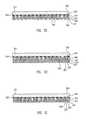
- FIG. 3Mshows the singulated multi-layer Direct Write Wafer Level Chip Scale Packaged electronic component of FIG. 3L in detail in accordance with the principles of one embodiment of the present invention
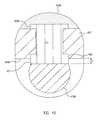
- FIG. 4Ashows a detail portion of a Direct Write Wafer Level Chip Scale Packaged electronic component wherein a dielectric layer has been ablated in such a way as to form patterned vias;
- FIG. 4Bshows a detail portion of a Direct Write Wafer Level Chip Scale Packaged electronic component wherein a metal buildup region is formed on bonding points of a conductive layer second surface.
- a method and structure according to one embodiment of the inventionprovides a Direct Write Wafer Level Chip Scale Package (DWWLCSP) that utilizes permanent coatings/layers and direct write techniques to pattern these coatings/layers.
- DWWLCSPDirect Write Wafer Level Chip Scale Package
- a Direct Write Wafer Level Chip Scale Package( 121 in FIG. 1H ) is created by first preparing a silicon wafer ( 100 in FIG. 1A ) and then a dielectric layer, also called a first dielectric layer, ( 107 in FIG. 1B ) is attached directly to the wafer. The dielectric layer is then ablated to form vias and trench patterns ( 104 in FIG. 1C ). In one embodiment of the invention, the dielectric layer ( 407 in FIG. 4B ) is ablated in such a way as to form patterned vias ( 411 in FIG. 4B ) to the die pads ( 498 in FIG. 4B ). The vias can be patterned in any way that the user of the invention deems necessary.
- a pattern of multiple smaller cylindrical or rectangular sub-vias( 416 A, 416 B, 416 C in FIG. 4A ) are formed.
- This particular structureprovides a cushion of dielectric material ( 407 A and 407 B) between sub-vias for thermal expansion and therefore provides better compliance properties between solder bumps, or other interconnections, and the surfaces of the dies comprising the silicon wafers.
- the surface of the dielectric layeris then plated with a conductive layer, also called a first conductive layer, ( 111 in FIG.
- the conductive layeris then partially removed through a controlled etching process, leaving only the conductor patterns and connections to the die pads ( FIG. 1E ). In one embodiment of the invention, these patterns are then processed through standard solder application techniques ( FIG. 1F ).
- a Direct Write Wafer Level Chip Scale Package( 221 in FIG. 2H ) is created by first preparing a silicon wafer ( 200 in FIG. 2A ) and then a dielectric layer, also called a first dielectric layer, ( 207 in FIG. 2B ) is attached to the wafer using an adhesive ( 204 in FIG. 2B ). The dielectric layer is then ablated to form via and trench patterns ( FIG. 2C ). In one embodiment of the invention, the dielectric layer is ablated in such a way as to form patterned vias to the die pads. The vias can be patterned in any way that the user of the invention deems necessary.
- a pattern of multiple smaller cylindrical or rectangular viasare formed.
- this particular structureprovides for thermal expansion and therefore provides better compliance properties between solder bumps, or other interconnections, and the surfaces of the dies comprising the silicon wafers.
- the surface of the dielectric layeris then plated with a conductive layer, also called a first conductive layer, ( 211 in FIG. 2D ), such as copper or another suitable conductive material, to fill in all of via and trench patterns and thereby form conductor patterns and connections to the die pads ( FIG. 2D ).
- the conductive layeris then partially removed through a controlled etching process, leaving only the conductor patterns and connections to the die pads ( FIG. 2E ). In one embodiment of the invention, these patterns are then processed through any standard solder application techniques ( FIG. 2F ).
- the dielectric and conductive layers of the inventioncan be laminated ( FIGS. 3A to 3M ), which enables the creation of multilayer Direct Write Wafer Level Chip Scale Package structures ( FIG. 3M ) at lower costs, and with improved reliability of the finished Direct Write Wafer Level Chip Scale Package.
- the Direct Write Wafer Level Chip Scale Packages of the inventioninclude dielectric and conductive materials applied directly onto the wafer surface.
- the dielectric layersare then ablated, as opposed to imaged using photolithography. Consequently, using the method and structure of the present invention.
- the materials usedneed not be photoimagable materials, thus saving the cost of the materials themselves and the cost of the masking and etching steps.
- the dielectric layerscan be attached to the wafer with an adhesive layer and this adhesive layer need not be patterned using standard techniques.
- the conductive layer building processis solely additive using the ablated dielectric layer as its mask. Consequently, the need for subsequent patterning and etching is eliminated.
- the materials usedneed not be photoimagable materials, the materials need not be of the prior art predetermined and specified thicknesses. Consequently, the resulting structures of the invention provide the opportunity for greater flexibility and “compliance” between solder bumps, or other interconnections, and the surfaces of the dies comprising the silicon wafers.
- the materials usedneed not be photoimagable materials, any one of numerous known adhesives and intermediate layer materials can be used with the method and structure of the invention.
- FIG. 1Ashows a silicon wafer 100 that has been prepared for the packaging process and includes bonding locations, or pads, 105 .
- silicon wafer 100has a silicon wafer first surface 101 and a silicon wafer second surface 103 .
- Silicon wafersare well known to those of skill in the art and typically include one or more electronic components, such as integrated circuits, (not shown) formed in, or on, silicon wafer 100 by methods well known to those of skill in the art.
- FIG. 1Bshows silicon wafer 100 of FIG. 1A including a dielectric layer, also called a first dielectric layer, 107 applied directly to silicon wafer second surface 103 of silicon wafer 100 in accordance with the principles of one embodiment of the present invention.
- a dielectric layer first surface 110 of dielectric layer 107is applied directly to silicon wafer second surface 103 of silicon wafer 100 .
- dielectric layer 107is a polymer layer.
- dielectric layer 107is made of InterVia® 8000 material and has a thickness of approximately forty ( 40 ) microns.
- InterVia® 8000 materialhas a thickness of approximately forty ( 40 ) microns.
- those of skill in the artwill readily recognize, in light of this disclosure, that many different types of materials and thicknesses can be used for dielectric layer 107 .
- dielectric layer 107is then ablated, using a laser or other ablation means, to form various predetermined patterns 104 in dielectric layer 107 .
- FIG. 1Cshows the structure of FIG. 1B after dielectric layer 107 has been ablated to form vias and trenches 104 in accordance with the principles of one embodiment of the present invention.
- dielectric layer 107is ablated in such a way as to form patterned vias to the die pads.
- the viascan be patterned in any way that the user of the invention deems necessary.
- a pattern or multiple smaller cylindrical or rectangular viasare formed.
- this particular structureprovides for thermal expansion and therefore provides better compliance properties between solder bumps, or other interconnections, and the surfaces of the dies comprising the silicon wafers.
- the Direct Write Wafer Level Chip Scale Packages of the inventioninclude dielectric layer 107 laminated directly onto the silicon wafer second surface 103 and the dielectric layer 107 is then ablated, as opposed to imaged using the photolithography techniques of the prior art. Consequently, using the method and structure of the present invention, the materials used need not be photoimagable materials.
- a conductive layer, also called a first conductive layer, 111is then applied to silicon wafer second surface 103 and dielectric layer second surface 109 .
- conductive layer 111is copper, or another suitable metal, and is applied to an approximate thickness of approximately five (5) microns above dielectric layer second surface 109 .
- conductive layer 111includes a conductive layer first surface 115 that is in electrical contact with bonding locations 105 and a conductive layer second surface 113 .
- conductive layer 111is then etched away in a controlled etch process that results in conductive layer second surface 113 being made level with dielectric layer second surface 109 .
- electrically conductive traces and vias 116are formed As discussed in more detail below with respect to FIG.
- portions of conductive layer second surface 113can, in one embodiment of the invention, be left higher that dielectric layer second surface 109 to facilitate better bonding and compliance.
- FIG. 1Eshows the structure of FIG. 1D after conductive layer 111 is etched using the controlled etching process in accordance with the principles of one embodiment of the present invention.
- Depth controlled etching processessuch as that used to bring conductive layer second surface 113 level with, or with potions slightly raised above, dielectric layer second surface 109 are well known to those of skill in the art and are therefore not discussed in further detail herein to avoid detracting from the present invention.
- the conductive layer 111 building processis solely additive using the ablated dielectric layer 107 as a mask. Consequently, the need for subsequent masks, patterning, and etching, as required in the prior art, is eliminated.
- the materials used for dielectric layer 107need not be photoimagable materials, the materials need not be of the prior art predetermined and specific thicknesses. Consequently, the resulting structures of the invention provide the opportunity for greater flexibility and “compliance” between solder bumps, or other interconnections, and the surfaces of the dies comprising the integrated circuit wafers.
- FIG. 1Fshows the structure of FIG. 1E with solder bumps 119 attached to selected bonding points 198 on conductive layer 111 using standard bumping techniques in accordance with the principles of one embodiment of the present invention.
- FIG. 1Gshows the structure of FIG. 1F being singulated into individual Direct Write Wafer Level Chip Scale Packaged electronic components 121 , 123 and 125 using a standard cutting means 127 such as a saw.
- FIG. 1Hshows a singulated Direct Write Wafer Level Chip Scale Packaged electronic component 121 in accordance with the principles of one embodiment of the present invention.
- a silicon wafer 200is first prepared for the packaging process, as discussed above.
- silicon wafer 200includes a silicon wafer first surface 201 , a silicon wafer second surface 203 , and bonding locations, or pads, 205 .
- an adhesive layer 204is applied to silicon wafer second surface 203 using methods well known to those of skill in the art such as spinning or spraying.
- FIG. 2Bshows the structure of FIG. 2A , including a dielectric layer, also called a first dielectric layer, 207 applied to silicon wafer second surface 203 using adhesive layer 204 of FIG. 2A .
- dielectric layer 207is then ablated, using a laser or other ablation means, to form various predetermined patterns 206 in dielectric layer 207 .
- dielectric layer 207is ablated in such a way as to form patterned vias to the die pads.
- the viascan be patterned in any way that the user of the invention deems necessary.
- FIG. 2Cshows silicon wafer 200 of FIG. 2B after dielectric layer 207 and adhesive layer 204 have been ablated to form vias and trenches 206 in accordance with the principles of one embodiment of the present invention.
- the Direct Write Wafer Level Chip Scale Packages of the inventioninclude dielectric layer 207 applied onto the silicon wafer second surface 203 and dielectric layer 207 is then ablated, as opposed to imaged using the photolithography techniques of the prior art. Consequently, using the method and structure of the present invention, the materials used need not be photoimagable materials.
- a conductive layeralso called a first conductive layer, 211 is then applied to silicon wafer second surface 203 and dielectric layer second surface 209 .
- conductive layer 211is copper, or another suitable metal, and is applied to an approximate thickness of five (5) microns above dielectric layer second surface 209 .
- conductive layer 211includes a conductive layer first surface 215 that is in electrical contact with bonding locations 205 and a conductive layer second surface 213 . According to the principles of one embodiment of the invention, conductive layer 211 is then etched away in a controlled etch process that results in conductive layer second surface 213 being made level with dielectric layer second surface 209 . In this way electrically conductive traces and vias 216 are formed. As discussed in more detail below with respect to FIG.
- portions of conductive layer second surface 213can, in one embodiment of the invention, be left higher than dielectric layer second surface 209 to facilitate better bonding and compliance.
- FIG. 2Eshows the structure of FIG. 2D after conductive layer 211 is etched using the controlled etching process in accordance with the principles of one embodiment of the present invention.
- Depth controlled etching processessuch as that used to bring conductive layer second surface 213 level with, or with selected portions raised above, dielectric layer second surface 209 are well known to those of skill in the art and are therefore not discussed in further detail herein to avoid detracting from the present invention.
- the conductive layer 211 building processis solely additive using the ablated dielectric layer 207 as a mask. Consequently, the need for subsequent masks, patterning, and etching, as required in the prior art, is eliminated.
- the materials used for dielectric layer 207need not be photoimagable materials, the materials need not be of the prior art predetermined and specific thicknesses. Consequently, the resulting structures of the invention provide the opportunity for greater flexibility and “compliance” between solder bumps, or other interconnections, and the surfaces of the dies comprising the integrated circuit wafers.
- FIG. 2Fshows the structure of FIG. 2E with solder bumps 219 attached to selected bonding points 298 on conductive layer 211 using standard bumping techniques in accordance with the principles of one embodiment of the present invention.
- FIG. 2Gshows the structure of FIG. 2F being singulated into individual Direct Write Wafer Level Chip Scale Packaged electronic components 221 , 223 and 225 using a standard cutting means 227 such as a saw.
- FIG. 2Hshows a singulated Direct Write Wafer Level Chip Scale Packaged electronic component 221 in accordance with the principles of one embodiment of the present invention.
- the permanent layers of the inventioni.e., the dielectric and conductive layers 107 , 207 and 111 , 211 respectively can be laminated or glued, which enables the creation of multilayer Direct Write Wafer Level Chip Scale Packaged electronic components at lower costs, and with improved reliability of the finished package.
- FIGS. 3A to 3Mshow the process and structure for a multilayer Direct Write Wafer Level Chip Scale Package in which a first dielectric layer is attached using an adhesive layer, such as discussed above with respect to FIGS. 2A to 2H , and a second dielectric layer is directly attached, such as discussed above with respect to FIGS. 1A to 1H .
- a silicon wafer 300is first prepared for the packaging process, as discussed above.
- silicon wafer 300includes a silicon wafer first surface 301 , a silicon wafer second surface 303 , and bonding locations or pads 305 .
- an adhesive layer 304is applied to silicon wafer second surface 303 using methods well known to those of skill in the art such as spinning or spraying.
- FIG. 3Bshows the structure of FIG. 3A , including a first dielectric layer 307 applied to silicon wafer second surface 303 using adhesive layer 304 of FIG. 3A .
- first dielectric layer 307is then ablated, using a laser or other ablation means, to form various predetermined patterns 306 in first dielectric layer 307 .
- FIG. 3Cshows silicon wafer 300 of FIG. 3B after first dielectric layer 307 has been ablated to form vias and trenches 306 in accordance with the principles of one embodiment of the present invention.
- one embodiment of the multilayer Direct Write Wafer Level Chip Scale Packages of the inventionincludes first dielectric layer 307 laminated directly onto the silicon wafer second surface 303 and first dielectric layer 307 is then ablated, as opposed to imaged using the photolithography techniques of the prior art. Consequently, using the method and structure of the present invention, the materials used need not be photoimagable materials.
- first layer of conductive material 311is then applied to silicon wafer second surface 303 and first dielectric layer second surface 309 of first dielectric layer 307 .
- first conductive layer 311is copper, or another suitable metal, and is applied to an approximate thickness of five (5) microns above first dielectric layer second surface 309 of first dielectric layer 307 .
- first conductive layer 311includes a first conductive layer first surface 315 that is in electrical contact with bonding locations 305 and a first conductive layer second surface 313 .
- first conductive layer 311is then etched away in a controlled etch process that results in first conductive layer second surface 313 of first conductive layer 311 being made level with first dielectric layer second surface 309 of first dielectric layer 307 .
- FIG. 3Eshows the structure of FIG. 3D after first conductive layer 311 is etched using the controlled etching process in accordance with the principles of one embodiment of the present invention.
- Depth controlled etching processescan be used to bring first conductive layer second surface 313 of first conductive layer 311 level with first dielectric layer second surface 309 of first dielectric layer 307 as well known to those of skill in the art and are therefore not discussed in further detail herein to avoid detracting from the present invention.
- the conductive layer 311 building processis solely additive using the ablated first dielectric layer 307 as its mask. Consequently, the need for subsequent masks, patterning, and etching, as required in the prior art, is eliminated using the present invention.
- FIG. 3Fshows the structure of FIG. 3E including a second dielectric layer 337 .
- a second dielectric layer first surface 336 of second dielectric layer 337is applied directly to first dielectric layer second surface 309 of first dielectric layer 307 and first conductive layer second surface 313 of first conductive layer 311 in accordance with the principles of one embodiment of the present invention.
- second dielectric layer 337is a polymer layer of InterVia° 8000, or a similar material having a thickness of forty ( 40 ) microns.
- InterVia° 8000or a similar material having a thickness of forty ( 40 ) microns.
- second dielectric layer 337is then ablated, using a laser or other ablation means, to form various predetermined patterns 344 in dielectric layer 337 .
- dielectric layer 337is ablated in such a way as to form patterned vias to the die pads.
- the viascan be patterned in any way that the user of the invention deems necessary. For instance, in one embodiment of the invention, rather than simply ablating a single cylindrical or rectangular via to the die pads, a pattern of multiple smaller cylindrical or rectangular vias are formed.
- FIG. 3Gshows the structure of FIG. 3F after second dielectric layer 337 has been ablated to form vias and trenches 344 in accordance with the principles of one embodiment of the present invention.
- a second conductive layer 345is then applied to second dielectric layer second surface 339 of second dielectric layer 337 .
- second conductive layer 345is copper, or another suitable metal, and is applied to an approximate thickness of five (5) microns or less.
- second conductive layer 345includes a second conductive layer first surface 346 that is in electrical contact with bonding locations 305 and a second conductive layer second surface 353 .
- second conductive layer 345is then etched away in a controlled etch process that results in second conductive layer second surface 353 of second conductive layer 345 being made level with second dielectric layer second surface 339 of second dielectric layer 337 .
- FIG. 3Ishows the structure of FIG. 3H after second conductive layer 345 is etched using the controlled etching process in accordance with the principles of one embodiment of the present invention.
- the second conductive layer 345 building processis solely additive using the ablated second dielectric layer 337 as a mask. Consequently, the need for subsequent masks, patterning, and etching, as required in the prior art, is eliminated.
- the materials used for second dielectric layer 337need not be photoimagable materials, the materials need not limited to the prior art predetermined and specific thicknesses. Consequently, the resulting structures of the invention provide the opportunity for greater flexibility and “compliance” between solder bumps, or other interconnections, and the surfaces of the dies comprising the integrated circuit wafers.
- FIG. 3Jshows the structure of FIG. 3I with solder bumps 319 attached to selected points on second conductive layer 345 using standard techniques in accordance with the principles of one embodiment of the present invention.
- FIG. 3Kshows the structure of FIG. 3J being singulated into individual multilayer Direct Write Wafer Level Chip Scale Packaged electronic components 321 , 323 and 325 using a standard cutting means 327 , such as a saw.
- FIG. 3Lshows a singulated multilayer Direct Write Wafer Level Chip Scale Packaged electronic component 321 in accordance with the principles of one embodiment of the present invention.
- FIG. 3Mshows the singulated multilayer Direct Write Wafer Level Chip Scale Packaged electronic component 321 of FIG. 3L in more detail.
- FIGS. 3A to 3MThe process and structure shown in FIGS. 3A to 3M is for a multilayer Direct Write Wafer Level Chip Scale Package 321 in which a first dielectric layer is attached using an adhesive layer, such as discussed above with respect to FIGS. 2A to 2H , and a second dielectric layer is directly attached, such as discussed above with respect to FIGS. 1A to 1H .
- a first dielectric layeris attached using an adhesive layer, such as discussed above with respect to FIGS. 2A to 2H
- a second dielectric layeris directly attached, such as discussed above with respect to FIGS. 1A to 1H .
- the multilayer Direct Write Wafer Level Chip Scale Packages of the inventioncan also be formed where all dielectric layers are attached using an adhesive layer, such as discussed above with respect to FIGS. 2A to 2H , or all dielectric layers are directly attached, such as discussed above with respect to FIGS. 1A to 1H .
- the dielectric layerssuch as dielectric layer 107 , dielectric layer 207 , and dielectric layer 337 are ablated in such a way as to form patterned vias to the die pads.
- the viascan be patterned in any way that the user of the invention deems necessary. For instance, in one embodiment of the invention, rather than simply ablating a single cylindrical or rectangular via to the die pads, a pattern of multiple smaller cylindrical or rectangular vias are formed. This particular structure provides for thermal expansion and therefore provides better compliance properties between solder bumps, or other interconnections, and the surfaces of the dies comprising the silicon wafers.
- FIG. 4Ashows a detail portion 400 A, such as portion 299 of FIG. 2F , of a Direct Write Wafer Level Chip Scale Packaged electronic component of the invention, such as Direct Write Wafer Level Chip Scale Packaged electronic component 121 or 221 discussed above, wherein a dielectric layer 407 , such as dielectric layer 107 or dielectric layer 207 discussed above, has it's dielectric layer second surface 409 A ablated in such a way as to form a patterned via 416 A, such as electrically conductive vias 116 and 216 discussed above, between bonding location or pad 405 , such as bonding locations or pads 105 and 205 discussed above, and bonding point 498 , such as bonding points 198 and 298 discussed above.
- a dielectric layer 407such as dielectric layer 107 or dielectric layer 207 discussed above
- a patterned via 416 Asuch as electrically conductive vias 116 and 216 discussed above
- patterned via 416includes multiple sub-vias 416 A, 416 B and 416 C as opposed to a single cylindrical or rectangular opening.
- This particular structureallows for better thermal expansion by providing dielectric columns 407 A and 407 B to absorb thermal expansion of sub-vias 416 A, 416 B and 416 C. Consequently, this particular embodiment of the invention provides better compliance properties between solder bump 419 and bonding point 498 and bonding location or pad 405 on the surfaces of the dies comprising the silicon wafers (not shown).
- portions of conductive layer second surfaces 113 , 213such as bonding points 198 and 298 for solder bumps 119 and 219 discussed above, and other interconnections, are be left higher that dielectric layer second surfaces 109 , 209 , respectively, to facilitate better bonding and compliance.
- FIG. 4Bshows detail portion 400 B, such as portion 299 of FIG. 2F , of a Direct Write Wafer Level Chip Scale Packaged electronic component of the invention, such as Direct Write Wafer Level Chip Scale Packaged electronic component 121 or 221 discussed above, wherein bonding point 498 includes a metal buildup region 451 that extends a height “h” above dielectric second surface 409 B.
- Metal buildup region 451is formed by either selective etching away of conductive layer second surfaces 113 , 213 (see FIGS. 1D and 1E and FIGS. 2D and 2E ) or by an additive process wherein metal buildup region 451 is applied after conductive layer second surface 113 or 213 is etched away.
- the present inventionprovides a method and structure for Direct Write Wafer Level Chip Scale Package (DWWLCSP) that utilizes permanent layers/coatings and direct write techniques to pattern these layers/coatings.
- DWWLCSPDirect Write Wafer Level Chip Scale Package
- the Direct Write Wafer Level Chip Scale Packages of the inventioninclude materials laminated directly onto the wafer surface. The layers are then ablated, as opposed to imaged using photolithography. Consequently, using the method and structure of the present invention, the materials used need not be photoimagable materials, thus saving the cost of the materials themselves and the cost of the masking steps.
- the dielectric layerscan be attached to the wafer with an adhesive layer and this adhesive layer need not be patterned using standard techniques.
- the metal layer building processis solely additive using the ablated dielectric layer as its mask. Consequently, the need for subsequent patterning and etching is eliminated.
- the materials usedneed not be photoimagable materials, the materials need not be limited to the prior art predetermined and specific thicknesses. Consequently, the resulting structures of the invention provide the opportunity for greater flexibility and “compliance” between solder bumps, or other interconnections, and the surfaces of the dies comprising the integrated circuit wafers.
Landscapes
- Engineering & Computer Science (AREA)
- Microelectronics & Electronic Packaging (AREA)
- Computer Hardware Design (AREA)
- Power Engineering (AREA)
- Manufacturing & Machinery (AREA)
- Physics & Mathematics (AREA)
- Condensed Matter Physics & Semiconductors (AREA)
- General Physics & Mathematics (AREA)
- Internal Circuitry In Semiconductor Integrated Circuit Devices (AREA)
Abstract
Description
Claims (7)
Priority Applications (2)
| Application Number | Priority Date | Filing Date | Title |
|---|---|---|---|
| US12/661,597US8188584B1 (en) | 2002-11-08 | 2010-03-19 | Direct-write wafer level chip scale package |
| US13/472,961US8501543B1 (en) | 2002-11-08 | 2012-05-16 | Direct-write wafer level chip scale package |
Applications Claiming Priority (5)
| Application Number | Priority Date | Filing Date | Title |
|---|---|---|---|
| US10/291,050US6905914B1 (en) | 2002-11-08 | 2002-11-08 | Wafer level package and fabrication method |
| US11/047,848US7247523B1 (en) | 2002-11-08 | 2005-01-31 | Two-sided wafer escape package |
| US28982605A | 2005-11-29 | 2005-11-29 | |
| US11/810,799US7723210B2 (en) | 2002-11-08 | 2007-06-06 | Direct-write wafer level chip scale package |
| US12/661,597US8188584B1 (en) | 2002-11-08 | 2010-03-19 | Direct-write wafer level chip scale package |
Related Parent Applications (1)
| Application Number | Title | Priority Date | Filing Date |
|---|---|---|---|
| US11/810,799DivisionUS7723210B2 (en) | 2002-11-08 | 2007-06-06 | Direct-write wafer level chip scale package |
Related Child Applications (1)
| Application Number | Title | Priority Date | Filing Date |
|---|---|---|---|
| US13/472,961DivisionUS8501543B1 (en) | 2002-11-08 | 2012-05-16 | Direct-write wafer level chip scale package |
Publications (1)
| Publication Number | Publication Date |
|---|---|
| US8188584B1true US8188584B1 (en) | 2012-05-29 |
Family
ID=46327997
Family Applications (2)
| Application Number | Title | Priority Date | Filing Date |
|---|---|---|---|
| US11/810,799Active2026-06-24US7723210B2 (en) | 2002-11-08 | 2007-06-06 | Direct-write wafer level chip scale package |
| US12/661,597ActiveUS8188584B1 (en) | 2002-11-08 | 2010-03-19 | Direct-write wafer level chip scale package |
Family Applications Before (1)
| Application Number | Title | Priority Date | Filing Date |
|---|---|---|---|
| US11/810,799Active2026-06-24US7723210B2 (en) | 2002-11-08 | 2007-06-06 | Direct-write wafer level chip scale package |
Country Status (1)
| Country | Link |
|---|---|
| US (2) | US7723210B2 (en) |
Cited By (16)
| Publication number | Priority date | Publication date | Assignee | Title |
|---|---|---|---|---|
| US20120032340A1 (en)* | 2010-08-06 | 2012-02-09 | Stats Chippac, Ltd. | Semiconductor Die and Method of Forming FO-WLCSP Vertical Interconnect Using TSV and TMV |
| US8486764B1 (en) | 2002-11-08 | 2013-07-16 | Amkor Technology, Inc. | Wafer level package and fabrication method |
| US8552548B1 (en) | 2011-11-29 | 2013-10-08 | Amkor Technology, Inc. | Conductive pad on protruding through electrode semiconductor device |
| US8786100B2 (en) | 2010-03-15 | 2014-07-22 | Stats Chippac, Ltd. | Semiconductor device and method of forming repassivation layer with reduced opening to contact pad of semiconductor die |
| US8846454B2 (en) | 2007-12-14 | 2014-09-30 | Stats Chippac, Ltd. | Semiconductor device and method of forming interconnect structure for encapsulated die having pre-applied protective layer |
| US8900995B1 (en) | 2010-10-05 | 2014-12-02 | Amkor Technology, Inc. | Semiconductor device and manufacturing method thereof |
| US8907476B2 (en) | 2010-03-12 | 2014-12-09 | Stats Chippac, Ltd. | Semiconductor device and method of forming sacrificial protective layer to protect semiconductor die edge during singulation |
| US9048298B1 (en) | 2012-03-29 | 2015-06-02 | Amkor Technology, Inc. | Backside warpage control structure and fabrication method |
| US9082833B1 (en) | 2011-01-06 | 2015-07-14 | Amkor Technology, Inc. | Through via recessed reveal structure and method |
| US9129943B1 (en) | 2012-03-29 | 2015-09-08 | Amkor Technology, Inc. | Embedded component package and fabrication method |
| US9159672B1 (en) | 2010-08-02 | 2015-10-13 | Amkor Technology, Inc. | Through via connected backside embedded circuit features structure and method |
| US9318441B2 (en) | 2007-12-14 | 2016-04-19 | Stats Chippac, Ltd. | Semiconductor device and method of forming sacrificial adhesive over contact pads of semiconductor die |
| US9548240B2 (en) | 2010-03-15 | 2017-01-17 | STATS ChipPAC Pte. Ltd. | Semiconductor device and method of forming repassivation layer for robust low cost fan-out semiconductor package |
| US9666500B2 (en) | 2007-12-14 | 2017-05-30 | STATS ChipPAC Pte. Ltd. | Semiconductor device and method of forming insulating layer disposed over the semiconductor die for stress relief |
| US20190035686A1 (en)* | 2017-07-25 | 2019-01-31 | Semiconductor Manufacturing International (Shanghai) Corporation | Packaging structure and fabrication method thereof |
| US20210280481A1 (en)* | 2020-03-03 | 2021-09-09 | Yangtze Memory Technologies Co., Ltd. | Protection structures in semiconductor chips and methods for forming the same |
Families Citing this family (5)
| Publication number | Priority date | Publication date | Assignee | Title |
|---|---|---|---|---|
| US8327532B2 (en)* | 2009-11-23 | 2012-12-11 | Freescale Semiconductor, Inc. | Method for releasing a microelectronic assembly from a carrier substrate |
| US9691734B1 (en) | 2009-12-07 | 2017-06-27 | Amkor Technology, Inc. | Method of forming a plurality of electronic component packages |
| US8324511B1 (en) | 2010-04-06 | 2012-12-04 | Amkor Technology, Inc. | Through via nub reveal method and structure |
| US8294276B1 (en) | 2010-05-27 | 2012-10-23 | Amkor Technology, Inc. | Semiconductor device and fabricating method thereof |
| US8791501B1 (en) | 2010-12-03 | 2014-07-29 | Amkor Technology, Inc. | Integrated passive device structure and method |
Citations (389)
| Publication number | Priority date | Publication date | Assignee | Title |
|---|---|---|---|---|
| US2596993A (en) | 1949-01-13 | 1952-05-20 | United Shoe Machinery Corp | Method and mold for covering of eyelets by plastic injection |
| US3435815A (en) | 1966-07-15 | 1969-04-01 | Micro Tech Mfg Inc | Wafer dicer |
| US3734660A (en) | 1970-01-09 | 1973-05-22 | Tuthill Pump Co | Apparatus for fabricating a bearing device |
| US3781596A (en) | 1972-07-07 | 1973-12-25 | R Galli | Semiconductor chip carriers and strips thereof |
| US3838984A (en) | 1973-04-16 | 1974-10-01 | Sperry Rand Corp | Flexible carrier and interconnect for uncased ic chips |
| US4054238A (en) | 1976-03-23 | 1977-10-18 | Western Electric Company, Inc. | Method, apparatus and lead frame for assembling leads with terminals on a substrate |
| US4189342A (en) | 1971-10-07 | 1980-02-19 | U.S. Philips Corporation | Semiconductor device comprising projecting contact layers |
| US4258381A (en) | 1977-12-07 | 1981-03-24 | Steag, Kernergie Gmbh | Lead frame for a semiconductor device suitable for mass production |
| US4289922A (en) | 1979-09-04 | 1981-09-15 | Plessey Incorporated | Integrated circuit package and lead frame |
| US4301464A (en) | 1978-08-02 | 1981-11-17 | Hitachi, Ltd. | Lead frame and semiconductor device employing the same with improved arrangement of supporting leads for securing the semiconductor supporting member |
| US4332537A (en) | 1978-07-17 | 1982-06-01 | Dusan Slepcevic | Encapsulation mold with removable cavity plates |
| US4417266A (en) | 1981-08-14 | 1983-11-22 | Amp Incorporated | Power and ground plane structure for chip carrier |
| US4451224A (en) | 1982-03-25 | 1984-05-29 | General Electric Company | Mold device for making plastic articles from resin |
| US4530152A (en) | 1982-04-01 | 1985-07-23 | Compagnie Industrielle Des Telecommunications Cit-Alcatel | Method for encapsulating semiconductor components using temporary substrates |
| US4541003A (en) | 1978-12-27 | 1985-09-10 | Hitachi, Ltd. | Semiconductor device including an alpha-particle shield |
| US4646710A (en) | 1982-09-22 | 1987-03-03 | Crystal Systems, Inc. | Multi-wafer slicing with a fixed abrasive |
| US4707724A (en) | 1984-06-04 | 1987-11-17 | Hitachi, Ltd. | Semiconductor device and method of manufacturing thereof |
| US4729061A (en) | 1985-04-29 | 1988-03-01 | Advanced Micro Devices, Inc. | Chip on board package for integrated circuit devices using printed circuit boards and means for conveying the heat to the opposite side of the package from the chip mounting side to permit the heat to dissipate therefrom |
| US4727633A (en) | 1985-08-08 | 1988-03-01 | Tektronix, Inc. | Method of securing metallic members together |
| US4737839A (en) | 1984-03-19 | 1988-04-12 | Trilogy Computer Development Partners, Ltd. | Semiconductor chip mounting system |
| US4756080A (en) | 1986-01-27 | 1988-07-12 | American Microsystems, Inc. | Metal foil semiconductor interconnection method |
| US4812896A (en) | 1986-11-13 | 1989-03-14 | Olin Corporation | Metal electronic package sealed with thermoplastic having a grafted metal deactivator and antioxidant |
| US4862246A (en) | 1984-09-26 | 1989-08-29 | Hitachi, Ltd. | Semiconductor device lead frame with etched through holes |
| US4862245A (en) | 1985-04-18 | 1989-08-29 | International Business Machines Corporation | Package semiconductor chip |
| US4907067A (en) | 1988-05-11 | 1990-03-06 | Texas Instruments Incorporated | Thermally efficient power device package |
| US4920074A (en) | 1987-02-25 | 1990-04-24 | Hitachi, Ltd. | Surface mount plastic package semiconductor integrated circuit, manufacturing method thereof, as well as mounting method and mounted structure thereof |
| US4935803A (en) | 1988-09-09 | 1990-06-19 | Motorola, Inc. | Self-centering electrode for power devices |
| US4942454A (en) | 1987-08-05 | 1990-07-17 | Mitsubishi Denki Kabushiki Kaisha | Resin sealed semiconductor device |
| US4987475A (en) | 1988-02-29 | 1991-01-22 | Digital Equipment Corporation | Alignment of leads for ceramic integrated circuit packages |
| US5018003A (en) | 1988-10-20 | 1991-05-21 | Mitsubishi Denki Kabushiki Kaisha | Lead frame and semiconductor device |
| US5029386A (en) | 1990-09-17 | 1991-07-09 | Hewlett-Packard Company | Hierarchical tape automated bonding method |
| US5041902A (en) | 1989-12-14 | 1991-08-20 | Motorola, Inc. | Molded electronic package with compression structures |
| US5057900A (en) | 1988-10-17 | 1991-10-15 | Semiconductor Energy Laboratory Co., Ltd. | Electronic device and a manufacturing method for the same |
| US5059379A (en) | 1987-07-20 | 1991-10-22 | Mitsubishi Denki Kabushiki Kaisha | Method of resin sealing semiconductor devices |
| US5065223A (en) | 1989-05-31 | 1991-11-12 | Fujitsu Vlsi Limited | Packaged semiconductor device |
| US5070039A (en) | 1989-04-13 | 1991-12-03 | Texas Instruments Incorporated | Method of making an integrated circuit using a pre-served dam bar to reduce mold flash and to facilitate flash removal |
| US5087961A (en) | 1987-01-28 | 1992-02-11 | Lsi Logic Corporation | Semiconductor device package |
| US5091341A (en) | 1989-05-22 | 1992-02-25 | Kabushiki Kaisha Toshiba | Method of sealing semiconductor device with resin by pressing a lead frame to a heat sink using an upper mold pressure member |
| US5096852A (en) | 1988-06-02 | 1992-03-17 | Burr-Brown Corporation | Method of making plastic encapsulated multichip hybrid integrated circuits |
| US5118298A (en) | 1991-04-04 | 1992-06-02 | Advanced Interconnections Corporation | Through hole mounting of integrated circuit adapter leads |
| US5122860A (en) | 1987-08-26 | 1992-06-16 | Matsushita Electric Industrial Co., Ltd. | Integrated circuit device and manufacturing method thereof |
| US5134773A (en) | 1989-05-26 | 1992-08-04 | Gerard Lemaire | Method for making a credit card containing a microprocessor chip |
| US5151039A (en) | 1990-04-06 | 1992-09-29 | Advanced Interconnections Corporation | Integrated circuit adapter having gullwing-shaped leads |
| US5157475A (en) | 1988-07-08 | 1992-10-20 | Oki Electric Industry Co., Ltd. | Semiconductor device having a particular conductive lead structure |
| US5157480A (en) | 1991-02-06 | 1992-10-20 | Motorola, Inc. | Semiconductor device having dual electrical contact sites |
| US5168368A (en) | 1991-05-09 | 1992-12-01 | International Business Machines Corporation | Lead frame-chip package with improved configuration |
| US5172213A (en) | 1991-05-23 | 1992-12-15 | At&T Bell Laboratories | Molded circuit package having heat dissipating post |
| US5172214A (en) | 1991-02-06 | 1992-12-15 | Motorola, Inc. | Leadless semiconductor device and method for making the same |
| US5175060A (en) | 1989-07-01 | 1992-12-29 | Ibiden Co., Ltd. | Leadframe semiconductor-mounting substrate having a roughened adhesive conductor circuit substrate and method of producing the same |
| US5200809A (en) | 1991-09-27 | 1993-04-06 | Vlsi Technology, Inc. | Exposed die-attach heatsink package |
| US5200362A (en) | 1989-09-06 | 1993-04-06 | Motorola, Inc. | Method of attaching conductive traces to an encapsulated semiconductor die using a removable transfer film |
| US5214845A (en) | 1992-05-11 | 1993-06-01 | Micron Technology, Inc. | Method for producing high speed integrated circuits |
| US5216278A (en) | 1990-12-04 | 1993-06-01 | Motorola, Inc. | Semiconductor device having a pad array carrier package |
| US5218231A (en) | 1989-08-30 | 1993-06-08 | Kabushiki Kaisha Toshiba | Mold-type semiconductor device |
| US5221642A (en) | 1991-08-15 | 1993-06-22 | Staktek Corporation | Lead-on-chip integrated circuit fabrication method |
| US5250843A (en) | 1991-03-27 | 1993-10-05 | Integrated System Assemblies Corp. | Multichip integrated circuit modules |
| US5250841A (en) | 1992-04-06 | 1993-10-05 | Motorola, Inc. | Semiconductor device with test-only leads |
| US5252853A (en) | 1991-09-19 | 1993-10-12 | Mitsubishi Denki Kabushiki Kaisha | Packaged semiconductor device having tab tape and particular power distribution lead structure |
| US5258094A (en) | 1991-09-18 | 1993-11-02 | Nec Corporation | Method for producing multilayer printed wiring boards |
| US5266834A (en) | 1989-03-13 | 1993-11-30 | Hitachi Ltd. | Semiconductor device and an electronic device with the semiconductor devices mounted thereon |
| US5268310A (en) | 1992-11-25 | 1993-12-07 | M/A-Com, Inc. | Method for making a mesa type PIN diode |
| US5277972A (en) | 1988-09-29 | 1994-01-11 | Tomoegawa Paper Co., Ltd. | Adhesive tapes |
| US5278446A (en) | 1992-07-06 | 1994-01-11 | Motorola, Inc. | Reduced stress plastic package |
| US5279029A (en) | 1990-08-01 | 1994-01-18 | Staktek Corporation | Ultra high density integrated circuit packages method |
| US5281849A (en) | 1991-05-07 | 1994-01-25 | Singh Deo Narendra N | Semiconductor package with segmented lead frame |
| US5294897A (en) | 1992-07-20 | 1994-03-15 | Mitsubishi Denki Kabushiki Kaisha | Microwave IC package |
| US5327008A (en) | 1993-03-22 | 1994-07-05 | Motorola Inc. | Semiconductor device having universal low-stress die support and method for making the same |
| US5332864A (en) | 1991-12-27 | 1994-07-26 | Vlsi Technology, Inc. | Integrated circuit package having an interposer |
| US5336931A (en) | 1993-09-03 | 1994-08-09 | Motorola, Inc. | Anchoring method for flow formed integrated circuit covers |
| US5335771A (en) | 1990-09-25 | 1994-08-09 | R. H. Murphy Company, Inc. | Spacer trays for stacking storage trays with integrated circuits |
| US5343076A (en) | 1990-07-21 | 1994-08-30 | Mitsui Petrochemical Industries, Ltd. | Semiconductor device with an airtight space formed internally within a hollow package |
| US5353498A (en) | 1993-02-08 | 1994-10-11 | General Electric Company | Method for fabricating an integrated circuit module |
| US5358905A (en) | 1993-04-02 | 1994-10-25 | Texas Instruments Incorporated | Semiconductor device having die pad locking to substantially reduce package cracking |
| US5365106A (en) | 1992-10-27 | 1994-11-15 | Kabushiki Kaisha Toshiba | Resin mold semiconductor device |
| US5381042A (en) | 1992-03-31 | 1995-01-10 | Amkor Electronics, Inc. | Packaged integrated circuit including heat slug having an exposed surface |
| EP0393997B1 (en) | 1989-04-20 | 1995-02-01 | Honeywell Inc. | Method of providing a variable-pitch leadframe assembly |
| US5391439A (en) | 1990-09-27 | 1995-02-21 | Dai Nippon Printing Co., Ltd. | Leadframe adapted to support semiconductor elements |
| US5394303A (en) | 1992-09-11 | 1995-02-28 | Kabushiki Kaisha Toshiba | Semiconductor device |
| US5406124A (en) | 1992-12-04 | 1995-04-11 | Mitsui Toatsu Chemicals, Inc. | Insulating adhesive tape, and lead frame and semiconductor device employing the tape |
| US5410180A (en) | 1992-07-28 | 1995-04-25 | Shinko Electric Industries Co., Ltd. | Metal plane support for multi-layer lead frames and a process for manufacturing such frames |
| US5414299A (en) | 1993-09-24 | 1995-05-09 | Vlsi Technology, Inc. | Semi-conductor device interconnect package assembly for improved package performance |
| US5417905A (en) | 1989-05-26 | 1995-05-23 | Esec (Far East) Limited | Method of making a card having decorations on both faces |
| US5428248A (en) | 1992-08-21 | 1995-06-27 | Goldstar Electron Co., Ltd. | Resin molded semiconductor package |
| US5432677A (en) | 1993-02-09 | 1995-07-11 | Texas Instruments Incorporated | Multi-chip integrated circuit module |
| US5435057A (en) | 1990-10-30 | 1995-07-25 | International Business Machines Corporation | Interconnection method and structure for organic circuit boards |
| US5444301A (en) | 1993-06-23 | 1995-08-22 | Goldstar Electron Co. Ltd. | Semiconductor package and method for manufacturing the same |
| US5452511A (en) | 1993-11-04 | 1995-09-26 | Chang; Alexander H. C. | Composite lead frame manufacturing method |
| US5454904A (en) | 1993-01-04 | 1995-10-03 | General Electric Company | Micromachining methods for making micromechanical moving structures including multiple contact switching system |
| US5454905A (en) | 1994-08-09 | 1995-10-03 | National Semiconductor Corporation | Method for manufacturing fine pitch lead frame |
| US5474958A (en) | 1993-05-04 | 1995-12-12 | Motorola, Inc. | Method for making semiconductor device having no die supporting surface |
| US5484274A (en) | 1992-11-24 | 1996-01-16 | Neu Dynamics Corp. | Encapsulation molding equipment |
| US5493151A (en) | 1993-07-15 | 1996-02-20 | Kabushiki Kaisha Toshiba | Semiconductor device, lead frame and method for manufacturing semiconductor devices |
| US5508556A (en) | 1994-09-02 | 1996-04-16 | Motorola, Inc. | Leaded semiconductor device having accessible power supply pad terminals |
| US5517056A (en) | 1993-09-30 | 1996-05-14 | Motorola, Inc. | Molded carrier ring leadframe having a particular resin injecting area design for gate removal and semiconductor device employing the same |
| US5521429A (en) | 1993-11-25 | 1996-05-28 | Sanyo Electric Co., Ltd. | Surface-mount flat package semiconductor device |
| US5528076A (en) | 1995-02-01 | 1996-06-18 | Motorola, Inc. | Leadframe having metal impregnated silicon carbide mounting area |
| US5534467A (en) | 1993-03-18 | 1996-07-09 | Lsi Logic Corporation | Semiconductor packages for high I/O semiconductor dies |
| US5539251A (en) | 1992-05-11 | 1996-07-23 | Micron Technology, Inc. | Tie bar over chip lead frame design |
| US5543657A (en) | 1994-10-07 | 1996-08-06 | International Business Machines Corporation | Single layer leadframe design with groundplane capability |
| US5544412A (en) | 1994-05-24 | 1996-08-13 | Motorola, Inc. | Method for coupling a power lead to a bond pad in an electronic module |
| US5545923A (en) | 1993-10-22 | 1996-08-13 | Lsi Logic Corporation | Semiconductor device assembly with minimized bond finger connections |
| US5576517A (en) | 1994-05-23 | 1996-11-19 | General Electric Company | Low Dielectric constant materials for high speed electronics |
| US5578525A (en) | 1993-12-13 | 1996-11-26 | Fujitsu Limited | Semiconductor device and a fabrication process thereof |
| US5581122A (en) | 1994-10-25 | 1996-12-03 | Industrial Technology Research Institute | Packaging assembly with consolidated common voltage connections for integrated circuits |
| US5592025A (en) | 1992-08-06 | 1997-01-07 | Motorola, Inc. | Pad array semiconductor device |
| US5592019A (en) | 1994-04-19 | 1997-01-07 | Mitsubishi Denki Kabushiki Kaisha | Semiconductor device and module |
| US5594274A (en) | 1993-07-01 | 1997-01-14 | Nec Corporation | Lead frame for use in a semiconductor device and method of manufacturing the semiconductor device using the same |
| US5595934A (en) | 1995-05-17 | 1997-01-21 | Samsung Electronics Co., Ltd. | Method for forming oxide protective film on bonding pads of semiconductor chips by UV/O3 treatment |
| US5604376A (en) | 1994-06-30 | 1997-02-18 | Digital Equipment Corporation | Paddleless molded plastic semiconductor chip package |
| US5608267A (en) | 1992-09-17 | 1997-03-04 | Olin Corporation | Molded plastic semiconductor package including heat spreader |
| US5608265A (en) | 1993-03-17 | 1997-03-04 | Hitachi, Ltd. | Encapsulated semiconductor device package having holes for electrically conductive material |
| US5619068A (en) | 1995-04-28 | 1997-04-08 | Lucent Technologies Inc. | Externally bondable overmolded package arrangements |
| US5625222A (en) | 1993-11-18 | 1997-04-29 | Fujitsu Limited | Semiconductor device in a resin package housed in a frame having high thermal conductivity |
| US5633528A (en) | 1994-05-25 | 1997-05-27 | Texas Instruments Incorporated | Lead frame structure for IC devices with strengthened encapsulation adhesion |
| US5639990A (en) | 1992-06-05 | 1997-06-17 | Mitsui Toatsu Chemicals, Inc. | Solid printed substrate and electronic circuit package using the same |
| US5640047A (en) | 1995-09-25 | 1997-06-17 | Mitsui High-Tec, Inc. | Ball grid assembly type semiconductor device having a heat diffusion function and an electric and magnetic shielding function |
| US5641997A (en) | 1993-09-14 | 1997-06-24 | Kabushiki Kaisha Toshiba | Plastic-encapsulated semiconductor device |
| US5643433A (en) | 1992-12-23 | 1997-07-01 | Shinko Electric Industries Co., Ltd. | Lead frame and method for manufacturing same |
| US5644169A (en) | 1993-03-04 | 1997-07-01 | Goldstar Electron Co., Ltd. | Mold and method for manufacturing a package for a semiconductor chip and the package manufactured thereby |
| US5646831A (en) | 1995-12-28 | 1997-07-08 | Vlsi Technology, Inc. | Electrically enhanced power quad flat pack arrangement |
| US5650663A (en) | 1995-07-03 | 1997-07-22 | Olin Corporation | Electronic package with improved thermal properties |
| US5661088A (en) | 1996-01-11 | 1997-08-26 | Motorola, Inc. | Electronic component and method of packaging |
| US5665996A (en) | 1994-12-30 | 1997-09-09 | Siliconix Incorporated | Vertical power mosfet having thick metal layer to reduce distributed resistance |
| EP0794572A2 (en) | 1996-03-07 | 1997-09-10 | Matsushita Electronics Corporation | Electronic component, method for making the same, and lead frame and mold assembly for use therein |
| US5673479A (en) | 1993-12-20 | 1997-10-07 | Lsi Logic Corporation | Method for mounting a microelectronic circuit peripherally-leaded package including integral support member with spacer |
| US5683806A (en) | 1988-09-29 | 1997-11-04 | Tomoegawa Paper Co., Ltd. | Adhesive tapes |
| US5689135A (en) | 1995-12-19 | 1997-11-18 | Micron Technology, Inc. | Multi-chip device and method of fabrication employing leads over and under processes |
| US5696666A (en) | 1995-10-11 | 1997-12-09 | Motorola, Inc. | Low profile exposed die chip carrier package |
| US5701034A (en) | 1994-05-03 | 1997-12-23 | Amkor Electronics, Inc. | Packaged semiconductor die including heat sink with locking feature |
| US5703407A (en) | 1995-02-14 | 1997-12-30 | Kabushiki Kaisha Toshiba | Resin-sealed type semiconductor device |
| US5710064A (en) | 1994-08-16 | 1998-01-20 | Samsung Electronics Co., Ltd. | Method for manufacturing a semiconductor package |
| US5724233A (en) | 1993-07-09 | 1998-03-03 | Fujitsu Limited | Semiconductor device having first and second semiconductor chips with a gap therebetween, a die stage in the gap and associated lead frames disposed in a package, the lead frames providing electrical connections from the chips to an exterior of the packag |
| US5723899A (en) | 1994-08-30 | 1998-03-03 | Amkor Electronics, Inc. | Semiconductor lead frame having connection bar and guide rings |
| US5726493A (en) | 1994-06-13 | 1998-03-10 | Fujitsu Limited | Semiconductor device and semiconductor device unit having ball-grid-array type package structure |
| US5736432A (en) | 1996-09-20 | 1998-04-07 | National Semiconductor Corporation | Lead frame with lead finger locking feature and method for making same |
| US5736448A (en) | 1995-12-04 | 1998-04-07 | General Electric Company | Fabrication method for thin film capacitors |
| US5745984A (en) | 1995-07-10 | 1998-05-05 | Martin Marietta Corporation | Method for making an electronic module |
| US5753977A (en) | 1996-03-22 | 1998-05-19 | Mitsubishi Denki Kabushiki Kaisha | Semiconductor device and lead frame therefor |
| US5753532A (en) | 1995-08-30 | 1998-05-19 | Samsung Electronics Co., Ltd. | Method of manufacturing semiconductor chip package |
| US5766972A (en) | 1994-06-02 | 1998-06-16 | Mitsubishi Denki Kabushiki Kaisha | Method of making resin encapsulated semiconductor device with bump electrodes |
| US5770888A (en) | 1995-12-29 | 1998-06-23 | Lg Semicon Co., Ltd. | Integrated chip package with reduced dimensions and leads exposed from the top and bottom of the package |
| US5769989A (en) | 1995-09-19 | 1998-06-23 | International Business Machines Corporation | Method and system for reworkable direct chip attach (DCA) structure with thermal enhancement |
| US5776798A (en) | 1996-09-04 | 1998-07-07 | Motorola, Inc. | Semiconductor package and method thereof |
| US5783861A (en) | 1994-03-29 | 1998-07-21 | Lg Semicon Co., Ltd. | Semiconductor package and lead frame |
| US5786238A (en) | 1997-02-13 | 1998-07-28 | Generyal Dynamics Information Systems, Inc. | Laminated multilayer substrates |
| US5801440A (en) | 1995-10-10 | 1998-09-01 | Acc Microelectronics Corporation | Chip package board having utility rings |
| US5814883A (en) | 1995-10-04 | 1998-09-29 | Mitsubishi Denki Kabushiki Kaisha | Packaged semiconductor chip |
| US5814884A (en) | 1996-10-24 | 1998-09-29 | International Rectifier Corporation | Commonly housed diverse semiconductor die |
| US5814881A (en) | 1996-12-20 | 1998-09-29 | Lsi Logic Corporation | Stacked integrated chip package and method of making same |
| US5818105A (en) | 1994-07-22 | 1998-10-06 | Nec Corporation | Semiconductor device with plastic material covering a semiconductor chip mounted on a substrate of the device |
| US5817540A (en) | 1996-09-20 | 1998-10-06 | Micron Technology, Inc. | Method of fabricating flip-chip on leads devices and resulting assemblies |
| US5821457A (en) | 1994-03-11 | 1998-10-13 | The Panda Project | Semiconductor die carrier having a dielectric epoxy between adjacent leads |
| US5821615A (en) | 1995-12-06 | 1998-10-13 | Lg Semicon Co., Ltd. | Semiconductor chip package having clip-type outlead and fabrication method of same |
| US5835988A (en) | 1996-03-27 | 1998-11-10 | Mitsubishi Denki Kabushiki Kaisha | Packed semiconductor device with wrap around external leads |
| US5834830A (en) | 1995-12-18 | 1998-11-10 | Lg Semicon Co., Ltd. | LOC (lead on chip) package and fabricating method thereof |
| US5841193A (en) | 1996-05-20 | 1998-11-24 | Epic Technologies, Inc. | Single chip modules, repairable multichip modules, and methods of fabrication thereof |
| US5844306A (en) | 1995-09-28 | 1998-12-01 | Mitsubishi Denki Kabushiki Kaisha | Die pad structure for solder bonding |
| US5856911A (en) | 1996-11-12 | 1999-01-05 | National Semiconductor Corporation | Attachment assembly for integrated circuits |
| US5859475A (en) | 1996-04-24 | 1999-01-12 | Amkor Technology, Inc. | Carrier strip and molded flex circuit ball grid array |
| US5859471A (en) | 1992-11-17 | 1999-01-12 | Shinko Electric Industries Co., Ltd. | Semiconductor device having tab tape lead frame with reinforced outer leads |
| US5866939A (en) | 1996-01-21 | 1999-02-02 | Anam Semiconductor Inc. | Lead end grid array semiconductor package |
| US5871782A (en) | 1995-12-30 | 1999-02-16 | Lg Semicon Co. Ltd. | Transfer molding apparatus having laminated chase block |
| US5874784A (en) | 1995-10-25 | 1999-02-23 | Sharp Kabushiki Kaisha | Semiconductor device having external connection terminals provided on an interconnection plate and fabrication process therefor |
| US5874770A (en) | 1996-10-10 | 1999-02-23 | General Electric Company | Flexible interconnect film including resistor and capacitor layers |
| US5877043A (en) | 1996-02-01 | 1999-03-02 | International Business Machines Corporation | Electronic package with strain relief means and method of making |
| US5886398A (en) | 1997-09-26 | 1999-03-23 | Lsi Logic Corporation | Molded laminate package with integral mold gate |
| US5886397A (en) | 1996-09-05 | 1999-03-23 | International Rectifier Corporation | Crushable bead on lead finger side surface to improve moldability |
| US5894108A (en) | 1997-02-11 | 1999-04-13 | National Semiconductor Corporation | Plastic package with exposed die |
| US5897339A (en) | 1996-09-11 | 1999-04-27 | Samsung Electronics Co., Ltd. | Lead-on-chip semiconductor device package having an adhesive layer formed from liquid adhesive and method for manufacturing the same |
| US5900676A (en) | 1996-08-19 | 1999-05-04 | Samsung Electronics Co., Ltd. | Semiconductor device package structure having column leads and a method for production thereof |
| US5903049A (en) | 1997-10-29 | 1999-05-11 | Mitsubishi Denki Kabushiki Kaisha | Semiconductor module comprising semiconductor packages |
| US5903050A (en) | 1998-04-30 | 1999-05-11 | Lsi Logic Corporation | Semiconductor package having capacitive extension spokes and method for making the same |
| US5915998A (en) | 1996-06-19 | 1999-06-29 | Erico International Corporation | Electrical connector and method of making |
| US5917242A (en) | 1996-05-20 | 1999-06-29 | Micron Technology, Inc. | Combination of semiconductor interconnect |
| US5937324A (en) | 1996-08-26 | 1999-08-10 | Motorola, Inc. | Method for forming a line-on-line multi-level metal interconnect structure for use in integrated circuits |
| US5939779A (en) | 1996-05-17 | 1999-08-17 | Lg Semicon Co., Ltd. | Bottom lead semiconductor chip stack package |
| US5942794A (en) | 1996-10-22 | 1999-08-24 | Matsushita Electronics Corporation | Plastic encapsulated semiconductor device and method of manufacturing the same |
| KR100220154B1 (en) | 1996-04-01 | 1999-09-01 | 김규현 | Method manufacture of semiconductor package |
| US5951305A (en) | 1998-07-09 | 1999-09-14 | Tessera, Inc. | Lidless socket and method of making same |
| US5959356A (en) | 1995-11-25 | 1999-09-28 | Samsung Electronics Co., Ltd. | Solder ball grid array carrier package with heat sink |
| US5969426A (en) | 1994-12-14 | 1999-10-19 | Mitsubishi Denki Kabushiki Kaisha | Substrateless resin encapsulated semiconductor device |
| US5973388A (en) | 1998-01-26 | 1999-10-26 | Motorola, Inc. | Leadframe, method of manufacturing a leadframe, and method of packaging an electronic component utilizing the leadframe |
| EP0844665A3 (en) | 1996-11-21 | 1999-10-27 | Texas Instruments Incorporated | Wafer level packaging |
| US5977615A (en) | 1996-12-24 | 1999-11-02 | Matsushita Electronics Corporation | Lead frame, method of manufacturing lead frame, semiconductor device and method of manufacturing semiconductor device |
| US5976912A (en) | 1994-03-18 | 1999-11-02 | Hitachi Chemical Company, Ltd. | Fabrication process of semiconductor package and semiconductor package |
| US5977630A (en) | 1997-08-15 | 1999-11-02 | International Rectifier Corp. | Plural semiconductor die housed in common package with split heat sink |
| US5982632A (en) | 1995-01-24 | 1999-11-09 | Intel Corporation | Short power signal path integrated circuit package |
| US5981314A (en) | 1996-10-31 | 1999-11-09 | Amkor Technology, Inc. | Near chip size integrated circuit package |
| US5986333A (en) | 1997-02-27 | 1999-11-16 | Oki Electric Industry Co., Ltd. | Semiconductor apparatus and method for fabricating the same |
| US5986885A (en) | 1997-04-08 | 1999-11-16 | Integrated Device Technology, Inc. | Semiconductor package with internal heatsink and assembly method |
| US6001671A (en) | 1996-04-18 | 1999-12-14 | Tessera, Inc. | Methods for manufacturing a semiconductor package having a sacrificial layer |
| US6013947A (en) | 1997-06-27 | 2000-01-11 | Trimecs Co., Ltd. | Substrate having gate recesses or slots and molding device and molding method thereof |
| US6018189A (en) | 1997-03-31 | 2000-01-25 | Nec Corporation | Lead frame for face-down bonding |
| US6020625A (en) | 1998-03-27 | 2000-02-01 | Mitsubishi Denki Kabushiki Kaisha | Lead frame including hanging leads and hanging lead reinforcement in a semiconductor device including the lead frame |
| US6025640A (en) | 1997-07-16 | 2000-02-15 | Dai Nippon Insatsu Kabushiki Kaisha | Resin-sealed semiconductor device, circuit member for use therein and method of manufacturing resin-sealed semiconductor device |
| US6031279A (en) | 1996-09-02 | 2000-02-29 | Siemens Aktiengesellschaft | Power semiconductor component |
| US6034423A (en) | 1998-04-02 | 2000-03-07 | National Semiconductor Corporation | Lead frame design for increased chip pinout |
| USRE36613E (en) | 1993-04-06 | 2000-03-14 | Micron Technology, Inc. | Multi-chip stacked devices |
| US6040626A (en) | 1998-09-25 | 2000-03-21 | International Rectifier Corp. | Semiconductor package |
| US6043430A (en) | 1997-03-14 | 2000-03-28 | Lg Semicon Co., Ltd. | Bottom lead semiconductor chip package |
| US6060768A (en) | 1995-05-09 | 2000-05-09 | Fujitsu Limited | Semiconductor device, method of manufacturing the semiconductor device, and method of manufacturing lead frame |
| JP2000150765A (en) | 1998-10-21 | 2000-05-30 | Amkor Technology Inc | Semiconductor integrated circuit plastic package, ultra- compact lead frame for manufacture thereof, and its manufacture |
| US6072228A (en) | 1996-10-25 | 2000-06-06 | Micron Technology, Inc. | Multi-part lead frame with dissimilar materials and method of manufacturing |
| US6075284A (en) | 1998-06-30 | 2000-06-13 | Hyundai Electronics Industries Co., Ltd. | Stack package |
| US6081029A (en) | 1998-03-12 | 2000-06-27 | Matsushita Electronics Corporation | Resin encapsulated semiconductor device having a reduced thickness and improved reliability |
| US6084310A (en) | 1997-04-21 | 2000-07-04 | Nec Corporation | Semiconductor device, lead frame, and lead bonding |
| US6087715A (en) | 1997-04-22 | 2000-07-11 | Kabushiki Kaisha Toshiba | Semiconductor device, and manufacturing method of the same |
| US6087722A (en) | 1998-05-28 | 2000-07-11 | Samsung Electronics Co., Ltd. | Multi-chip package |
| US6097089A (en) | 1998-01-28 | 2000-08-01 | Mitsubishi Gas Chemical Company, Inc. | Semiconductor plastic package, metal plate for said package, and method of producing copper-clad board for said package |
| US6100594A (en) | 1998-01-14 | 2000-08-08 | Sharp Kabushiki Kaisha | Semiconductor device and method of manufacturing the same |
| US6114752A (en) | 1998-11-10 | 2000-09-05 | Siliconware Precision Industries Co., Ltd. | Semiconductor package having lead frame with an exposed base pad |
| US6113474A (en) | 1997-10-01 | 2000-09-05 | Cummins Engine Company, Inc. | Constant force truing and dressing apparatus and method |
| US6118184A (en) | 1997-07-18 | 2000-09-12 | Sharp Kabushiki Kaisha | Semiconductor device sealed with a sealing resin and including structure to balance sealing resin flow |
| US6118174A (en) | 1996-12-28 | 2000-09-12 | Lg Semicon Co., Ltd. | Bottom lead frame and bottom lead semiconductor package using the same |
| US6127633A (en) | 1995-04-28 | 2000-10-03 | Victor Company Of Japan, Ltd. | Multilayer print circuit board having a blind hole in an insulation layer with a roughened surface formed by application of an oxidizing agent and method of production |
| US6130473A (en) | 1998-04-02 | 2000-10-10 | National Semiconductor Corporation | Lead frame chip scale package |
| USRE36907E (en) | 1992-12-07 | 2000-10-10 | Integrated Device Technology, Inc. | Leadframe with power and ground planes |
| US6133623A (en) | 1996-07-03 | 2000-10-17 | Seiko Epson Corporation | Resin sealing type semiconductor device that includes a plurality of leads and method of making the same |
| US6143981A (en) | 1998-06-24 | 2000-11-07 | Amkor Technology, Inc. | Plastic integrated circuit package and method and leadframe for making the package |
| US6154366A (en) | 1999-11-23 | 2000-11-28 | Intel Corporation | Structures and processes for fabricating moisture resistant chip-on-flex packages |
| US6169329B1 (en) | 1996-04-02 | 2001-01-02 | Micron Technology, Inc. | Semiconductor devices having interconnections using standardized bonding locations and methods of designing |
| US6177718B1 (en) | 1998-04-28 | 2001-01-23 | Kabushiki Kaisha Toshiba | Resin-sealed semiconductor device |
| US6181002B1 (en) | 1998-12-22 | 2001-01-30 | Sharp Kabushiki Kaisha | Semiconductor device having a plurality of semiconductor chips |
| US6184573B1 (en) | 1999-05-13 | 2001-02-06 | Siliconware Precision Industries Co., Ltd. | Chip packaging |
| US6184465B1 (en) | 1998-11-12 | 2001-02-06 | Micron Technology, Inc. | Semiconductor package |
| US6194777B1 (en) | 1998-06-27 | 2001-02-27 | Texas Instruments Incorporated | Leadframes with selective palladium plating |
| US6194250B1 (en) | 1998-09-14 | 2001-02-27 | Motorola, Inc. | Low-profile microelectronic package |
| US6198171B1 (en) | 1999-12-30 | 2001-03-06 | Siliconware Precision Industries Co., Ltd. | Thermally enhanced quad flat non-lead package of semiconductor |
| JP2001060648A (en) | 1999-08-23 | 2001-03-06 | Dainippon Printing Co Ltd | Lead frame, method of manufacturing the same, and semiconductor device |
| US6197615B1 (en) | 1997-04-04 | 2001-03-06 | Samsung Electronics Co., Ltd. | Method of producing lead frame having uneven surfaces |
| US6201186B1 (en) | 1998-06-29 | 2001-03-13 | Motorola, Inc. | Electronic component assembly and method of making the same |
| US6201292B1 (en) | 1997-04-02 | 2001-03-13 | Dai Nippon Insatsu Kabushiki Kaisha | Resin-sealed semiconductor device, circuit member used therefor |
| US6204554B1 (en) | 1996-09-05 | 2001-03-20 | International Rectifier Corporation | Surface mount semiconductor package |
| US6208021B1 (en) | 1996-03-27 | 2001-03-27 | Oki Electric Industry Co., Ltd. | Semiconductor device, manufacturing method thereof and aggregate type semiconductor device |
| US6208023B1 (en) | 1997-07-31 | 2001-03-27 | Matsushita Electronics Corporation | Lead frame for use with an RF powered semiconductor |
| US6208020B1 (en) | 1999-02-24 | 2001-03-27 | Matsushita Electronics Corporation | Leadframe for use in manufacturing a resin-molded semiconductor device |
| US6211462B1 (en) | 1998-11-05 | 2001-04-03 | Texas Instruments Incorporated | Low inductance power package for integrated circuits |
| US6214525B1 (en) | 1996-09-06 | 2001-04-10 | International Business Machines Corp. | Printed circuit board with circuitized cavity and methods of producing same |
| US6217987B1 (en) | 1996-11-20 | 2001-04-17 | Ibiden Co. Ltd. | Solder resist composition and printed circuit boards |
| US6218731B1 (en) | 1999-05-21 | 2001-04-17 | Siliconware Precision Industries Co., Ltd. | Tiny ball grid array package |
| US6222259B1 (en) | 1998-09-15 | 2001-04-24 | Hyundai Electronics Industries Co., Ltd. | Stack package and method of fabricating the same |
| US6222258B1 (en) | 1996-11-11 | 2001-04-24 | Fujitsu Limited | Semiconductor device and method for producing a semiconductor device |
| US6221754B1 (en) | 1998-08-21 | 2001-04-24 | United Microelectronics Corp. | Method of fabricating a plug |
| JP2001118947A (en) | 1999-10-19 | 2001-04-27 | Nec Corp | Semiconductor device and method of manufacturing package therefor |
| US6229205B1 (en) | 1997-06-30 | 2001-05-08 | Samsung Electronics Co., Ltd. | Semiconductor device package having twice-bent tie bar and small die pad |
| US6229200B1 (en) | 1998-06-10 | 2001-05-08 | Asat Limited | Saw-singulated leadless plastic chip carrier |
| US6239384B1 (en) | 1995-09-18 | 2001-05-29 | Tessera, Inc. | Microelectric lead structures with plural conductors |
| US6239367B1 (en) | 1999-01-29 | 2001-05-29 | United Microelectronics Corp. | Multi-chip chip scale package |
| US6256200B1 (en) | 1999-05-27 | 2001-07-03 | Allen K. Lam | Symmetrical package for semiconductor die |
| US6258629B1 (en) | 1999-08-09 | 2001-07-10 | Amkor Technology, Inc. | Electronic device package and leadframe and method for making the package |
| US6258192B1 (en) | 1999-02-10 | 2001-07-10 | International Business Machines Corporation | Multi-thickness, multi-layer green sheet processing |
| US6261918B1 (en) | 1999-10-04 | 2001-07-17 | Conexant Systems, Inc. | Method for creating and preserving alignment marks for aligning mask layers in integrated circuit manufacture |
| US20010008305A1 (en) | 1998-06-10 | 2001-07-19 | Asat Ltd. | Leadless plastic chip carrier with etch back pad singulation |
| US20010011654A1 (en) | 1998-07-16 | 2001-08-09 | The University Of Texas System | Method for rapid drying of coated materials with close capture of vapors |
| US20010012704A1 (en) | 1998-07-13 | 2001-08-09 | Benjamin N. Eldridge | Interconnect assemblies and methods |
| US20010014538A1 (en) | 1998-06-10 | 2001-08-16 | Asat Ltd. | Leadless plastic chip carrier with etch back pad singulation and die attach pad array |
| EP0459493B1 (en) | 1990-06-01 | 2001-08-16 | Kabushiki Kaisha Toshiba | A semiconductor device comprising a TAB tape and its manufacturing method |
| US6281566B1 (en) | 1996-09-30 | 2001-08-28 | Sgs-Thomson Microelectronics S.R.L. | Plastic package for electronic devices |
| US6282095B1 (en) | 1999-02-02 | 2001-08-28 | Compaq Computer Corporation | Method and system for controlling radio frequency radiation in microelectronic packages using heat dissipation structures |
| US6285075B1 (en) | 1998-11-02 | 2001-09-04 | Asat, Limited | Integrated circuit package with bonding planes on a ceramic ring using an adhesive assembly |
| US6291273B1 (en) | 1996-12-26 | 2001-09-18 | Hitachi, Ltd. | Plastic molded type semiconductor device and fabrication process thereof |
| US6291271B1 (en) | 1999-09-14 | 2001-09-18 | Advanced Semiconductor Engineering, Inc. | Method of making semiconductor chip package |
| US6294100B1 (en) | 1998-06-10 | 2001-09-25 | Asat Ltd | Exposed die leadless plastic chip carrier |
| US6295977B1 (en) | 1998-11-05 | 2001-10-02 | Wacker Chemie Gmbh | Method and device for simultaneously cutting off a multiplicity of wafers from a workpiece |
| US6297548B1 (en) | 1998-06-30 | 2001-10-02 | Micron Technology, Inc. | Stackable ceramic FBGA for high thermal applications |
| US6303997B1 (en) | 1998-04-08 | 2001-10-16 | Anam Semiconductor, Inc. | Thin, stackable semiconductor packages |
| US6303984B1 (en) | 1997-08-12 | 2001-10-16 | Micron Technology, Inc. | Lead frame including angle iron tie bar |
| US6307272B1 (en) | 1998-05-27 | 2001-10-23 | Hitachi, Ltd. | Semiconductor device and method for manufacturing the same |
| US6309909B1 (en) | 1998-07-02 | 2001-10-30 | Mitsubishi Denki Kabushiki Kaisha | Semiconductor device and method of manufacturing the same |
| US6316838B1 (en) | 1999-10-29 | 2001-11-13 | Fujitsu Limited | Semiconductor device |
| US6316822B1 (en) | 1998-09-16 | 2001-11-13 | Texas Instruments Incorporated | Multichip assembly semiconductor |
| US6323550B1 (en) | 1995-06-06 | 2001-11-27 | Analog Devices, Inc. | Package for sealing an integrated circuit die |
| US6326243B1 (en) | 1995-08-15 | 2001-12-04 | Kabushiki Kaisha Toshiba | Resin sealed semiconductor device including a die pad uniformly having heat conducting paths and circulating holes for fluid resin |
| US6326678B1 (en) | 1993-09-03 | 2001-12-04 | Asat, Limited | Molded plastic package with heat sink and enhanced electrical performance |
| US6326244B1 (en) | 1998-09-03 | 2001-12-04 | Micron Technology, Inc. | Method of making a cavity ball grid array apparatus |
| US6335564B1 (en) | 1998-05-06 | 2002-01-01 | Conexant Systems, Inc. | Single Paddle having a semiconductor device and a passive electronic component |
| US6337510B1 (en) | 2000-11-17 | 2002-01-08 | Walsin Advanced Electronics Ltd | Stackable QFN semiconductor package |
| US6339255B1 (en) | 1998-10-24 | 2002-01-15 | Hyundai Electronics Industries Co., Ltd. | Stacked semiconductor chips in a single semiconductor package |
| JP2002043497A (en) | 2000-07-27 | 2002-02-08 | Mitsubishi Electric Corp | Semiconductor device |
| US6348726B1 (en) | 2001-01-18 | 2002-02-19 | National Semiconductor Corporation | Multi row leadless leadframe package |
| US20020024122A1 (en) | 2000-08-25 | 2002-02-28 | Samsung Electronics Co., Ltd. | Lead frame having a side ring pad and semiconductor chip package including the same |
| US20020027297A1 (en) | 2000-09-04 | 2002-03-07 | Chikao Ikenaga | Semiconductor package |
| US6355502B1 (en) | 2000-04-25 | 2002-03-12 | National Science Council | Semiconductor package and method for making the same |
| US6365974B1 (en) | 1999-03-23 | 2002-04-02 | Texas Instruments Incorporated | Flex circuit substrate for an integrated circuit package |
| US6369454B1 (en) | 1998-12-31 | 2002-04-09 | Amkor Technology, Inc. | Semiconductor package and method for fabricating the same |
| US6369447B2 (en) | 1998-04-20 | 2002-04-09 | Mitsubishi Denki Kabushiki Kaisha | Plastic-packaged semiconductor device including a plurality of chips |
| US6373127B1 (en) | 1998-09-29 | 2002-04-16 | Texas Instruments Incorporated | Integrated capacitor on the back of a chip |
| US6380048B1 (en) | 2001-08-02 | 2002-04-30 | St Assembly Test Services Pte Ltd | Die paddle enhancement for exposed pad in semiconductor packaging |
| US6384472B1 (en) | 2000-03-24 | 2002-05-07 | Siliconware Precision Industries Co., Ltd | Leadless image sensor package structure and method for making the same |
| US6388336B1 (en) | 1999-09-15 | 2002-05-14 | Texas Instruments Incorporated | Multichip semiconductor assembly |
| US20020061642A1 (en) | 1999-09-02 | 2002-05-23 | Matsushita Electric Industrial Co., Ltd. | Semiconductor device and method of manufacturing the same |
| US6396148B1 (en) | 2000-02-10 | 2002-05-28 | Epic Technologies, Inc. | Electroless metal connection structures and methods |
| US6395578B1 (en) | 1999-05-20 | 2002-05-28 | Amkor Technology, Inc. | Semiconductor package and method for fabricating the same |
| US6396153B2 (en) | 1999-10-04 | 2002-05-28 | General Electric Company | Circuit chip package and fabrication method |
| US6400004B1 (en) | 2000-08-17 | 2002-06-04 | Advanced Semiconductor Engineering, Inc. | Leadless semiconductor package |
| US6410979B2 (en) | 1998-12-21 | 2002-06-25 | Nec Corporation | Ball-grid-array semiconductor device with protruding terminals |
| KR20020049944A (en) | 2000-12-20 | 2002-06-26 | 박종섭 | semiconductor package and method for fabricating the same |
| US6414385B1 (en) | 1999-11-08 | 2002-07-02 | Siliconware Precisionindustries Co., Ltd. | Quad flat non-lead package of semiconductor |
| US6418615B1 (en) | 1999-03-11 | 2002-07-16 | Shinko Electronics Industries, Co., Ltd. | Method of making multilayered substrate for semiconductor device |
| US6420779B1 (en) | 1999-09-14 | 2002-07-16 | St Assembly Test Services Ltd. | Leadframe based chip scale package and method of producing the same |
| US6429508B1 (en) | 2000-08-09 | 2002-08-06 | Kostat Semiconductor Co., Ltd. | Semiconductor package having implantable conductive lands and method for manufacturing the same |
| US6437429B1 (en) | 2001-05-11 | 2002-08-20 | Walsin Advanced Electronics Ltd | Semiconductor package with metal pads |
| US6444499B1 (en) | 2000-03-30 | 2002-09-03 | Amkor Technology, Inc. | Method for fabricating a snapable multi-package array substrate, snapable multi-package array and snapable packaged electronic components |
| US6448633B1 (en) | 1998-11-20 | 2002-09-10 | Amkor Technology, Inc. | Semiconductor package and method of making using leadframe having lead locks to secure leads to encapsulant |
| US6452279B2 (en) | 2000-07-14 | 2002-09-17 | Mitsubishi Denki Kabushiki Kaisha | Semiconductor device |
| US6459148B1 (en) | 2000-11-13 | 2002-10-01 | Walsin Advanced Electronics Ltd | QFN semiconductor package |
| US20020140068A1 (en) | 2001-03-28 | 2002-10-03 | Ming-Hsun Lee | Leadframe-based semiconductor package for multi-media card |
| US20020140061A1 (en) | 2001-03-27 | 2002-10-03 | Lee Hyung Ju | Lead frame for semiconductor package |
| US6464121B2 (en) | 2000-12-21 | 2002-10-15 | Xerox Corporation | Specialized tool adapted for a process for manufacture and interconnection between adjoining printed wiring boards |
| US6476474B1 (en) | 2000-10-10 | 2002-11-05 | Siliconware Precision Industries Co., Ltd. | Dual-die package structure and method for fabricating the same |
| US6476469B2 (en) | 2000-11-23 | 2002-11-05 | Siliconware Precision Industries Co., Ltd. | Quad flat non-leaded package structure for housing CMOS sensor |
| US20020163015A1 (en) | 2001-02-27 | 2002-11-07 | Chippac, Inc. | Plastic semiconductor package |
| US6482680B1 (en) | 2001-07-20 | 2002-11-19 | Carsem Semiconductor Sdn, Bhd. | Flip-chip on lead frame |
| US6486005B1 (en) | 2000-04-03 | 2002-11-26 | Hynix Semiconductor Inc. | Semiconductor package and method for fabricating the same |
| US6498099B1 (en) | 1998-06-10 | 2002-12-24 | Asat Ltd. | Leadless plastic chip carrier with etch back pad singulation |
| US6498392B2 (en) | 2000-01-24 | 2002-12-24 | Nec Corporation | Semiconductor devices having different package sizes made by using common parts |
| US6507096B2 (en) | 2000-08-09 | 2003-01-14 | Kostat Semiconductor Co., Ltd. | Tape having implantable conductive lands for semiconductor packaging process and method for manufacturing the same |
| US6507120B2 (en) | 2000-12-22 | 2003-01-14 | Siliconware Precision Industries Co., Ltd. | Flip chip type quad flat non-leaded package |
| US20030013232A1 (en) | 2001-07-11 | 2003-01-16 | Intel Corporation | Method for fabricating a microelectronic device using wafer-level adhesion layer deposition |
| US20030030131A1 (en) | 2000-09-15 | 2003-02-13 | Samsung Techwin Co., Ltd., | Semiconductor package apparatus and method |
| US6521530B2 (en) | 1998-11-13 | 2003-02-18 | Fujitsu Limited | Composite interposer and method for producing a composite interposer |
| US6524885B2 (en) | 2000-12-15 | 2003-02-25 | Eaglestone Partners I, Llc | Method, apparatus and system for building an interposer onto a semiconductor wafer using laser techniques |
| US20030064548A1 (en) | 2000-06-21 | 2003-04-03 | Isaak Harlan R. | Panel stacking of BGA devices to form three-dimensional modules |
| US6545345B1 (en) | 2001-03-20 | 2003-04-08 | Amkor Technology, Inc. | Mounting for a package containing a chip |
| US6545332B2 (en) | 2001-01-17 | 2003-04-08 | Siliconware Precision Industries Co., Ltd. | Image sensor of a quad flat package |
| US6549891B1 (en) | 1996-03-26 | 2003-04-15 | Recovery Management Corporation | Method for managing inventory |
| US6548898B2 (en) | 2000-12-28 | 2003-04-15 | Fujitsu Limited | External connection terminal and semiconductor device |
| US20030073265A1 (en) | 2001-10-12 | 2003-04-17 | Tom Hu | Semiconductor package with singulation crease |
| US6559525B2 (en) | 2000-01-13 | 2003-05-06 | Siliconware Precision Industries Co., Ltd. | Semiconductor package having heat sink at the outer surface |
| EP0936671B1 (en) | 1998-02-12 | 2003-05-07 | Hitachi, Ltd. | Resin-moulded semiconductor hybrid module and manufacturing method thereof |
| US6583503B2 (en) | 1997-03-10 | 2003-06-24 | Micron Technology, Inc. | Semiconductor package with stacked substrates and multiple semiconductor dice |
| US6593645B2 (en) | 1999-09-24 | 2003-07-15 | United Microelectronics Corp. | Three-dimensional system-on-chip structure |
| US20030134455A1 (en) | 2002-01-15 | 2003-07-17 | Jao-Chin Cheng | Method of forming IC package having upward-facing chip cavity |
| US6624005B1 (en) | 2000-09-06 | 2003-09-23 | Amkor Technology, Inc. | Semiconductor memory cards and method of making same |
| US6667546B2 (en) | 2001-11-15 | 2003-12-23 | Siliconware Precision Industries Co., Ltd. | Ball grid array semiconductor package and substrate without power ring or ground ring |
| US6671398B2 (en) | 1998-09-09 | 2003-12-30 | Applied Materials, Inc. | Method and apparatus for inspection of patterned semiconductor wafers |
| US20040004293A1 (en) | 2001-04-27 | 2004-01-08 | Shinko Electric Industries Co., Ltd | Semiconductor package |
| US6680529B2 (en) | 2002-02-15 | 2004-01-20 | Advanced Semiconductor Engineering, Inc. | Semiconductor build-up package |
| KR20040012028A (en) | 2002-07-31 | 2004-02-11 | 앰코 테크놀로지 코리아 주식회사 | chip size package |
| US20040026781A1 (en) | 2001-09-28 | 2004-02-12 | Toru Nakai | Printed wiring board and production method for printed wiring board |
| US20040046244A1 (en) | 2001-10-31 | 2004-03-11 | Shinko Electric Industries Co., Ltd. | Multilayered substrate for semiconductor device |
| US20040056277A1 (en) | 2002-09-17 | 2004-03-25 | Chippac, Inc. | Semiconductor multi-package module including stacked-die package and having wire bond interconnect between stacked packages |
| US20040063242A1 (en) | 2002-09-17 | 2004-04-01 | Chippac, Inc. | Semiconductor multi-package module having package stacked over ball grid array package and having wire bond interconnect between stacked packages |
| US20040061213A1 (en) | 2002-09-17 | 2004-04-01 | Chippac, Inc. | Semiconductor multi-package module having package stacked over die-up flip chip ball grid array package and having wire bond interconnect between stacked packages |
| US20040063246A1 (en) | 2002-09-17 | 2004-04-01 | Chippac, Inc. | Semiconductor multi-package module having package stacked over die-down flip chip ball grid array package and having wire bond interconnect between stacked packages |
| US20040061212A1 (en) | 2002-09-17 | 2004-04-01 | Chippac, Inc. | Semiconductor multi-package module having wire bond interconnect between stacked packages |
| US6727576B2 (en) | 2001-10-31 | 2004-04-27 | Infineon Technologies Ag | Transfer wafer level packaging |
| US6730857B2 (en) | 2001-03-13 | 2004-05-04 | International Business Machines Corporation | Structure having laser ablated features and method of fabricating |
| US6740964B2 (en) | 2000-11-17 | 2004-05-25 | Oki Electric Industry Co., Ltd. | Semiconductor package for three-dimensional mounting, fabrication method thereof, and semiconductor device |
| US20040113260A1 (en) | 2002-11-26 | 2004-06-17 | Shinko Electric Industries Co., Ltd. | Electronic parts packaging structure and method of manufacturing the same |
| DE19734794B4 (en) | 1997-01-09 | 2004-09-23 | Mitsubishi Denki K.K. | A lead frame with a plurality of wiring parts for use in a semiconductor device |
| EP0720225B1 (en) | 1994-12-30 | 2004-10-27 | SILICONIX Incorporated | Lateral power MOSFET having metal strap layer to reduce distributed resistance and method of fabricating the same |
| US6831371B1 (en) | 2002-03-16 | 2004-12-14 | Amkor Technology, Inc. | Integrated circuit substrate having embedded wire conductors and method therefor |
| US6838776B2 (en) | 2003-04-18 | 2005-01-04 | Freescale Semiconductor, Inc. | Circuit device with at least partial packaging and method for forming |
| US20050001309A1 (en) | 2003-06-20 | 2005-01-06 | Akinori Tanaka | Printed wiring board for mounting semiconductor |
| US6845554B2 (en) | 2001-11-22 | 2005-01-25 | Infineon Technologies Ag | Method for connection of circuit units |
| US6853060B1 (en) | 2003-04-22 | 2005-02-08 | Amkor Technology, Inc. | Semiconductor package using a printed circuit board and a method of manufacturing the same |
| US20050124093A1 (en) | 2003-12-03 | 2005-06-09 | Wen-Kun Yang | Fan out type wafer level package structure and method of the same |
| US6905914B1 (en) | 2002-11-08 | 2005-06-14 | Amkor Technology, Inc. | Wafer level package and fabrication method |
| US6921975B2 (en) | 2003-04-18 | 2005-07-26 | Freescale Semiconductor, Inc. | Circuit device with at least partial packaging, exposed active surface and a voltage reference plane |
| US6930256B1 (en) | 2002-05-01 | 2005-08-16 | Amkor Technology, Inc. | Integrated circuit substrate having laser-embedded conductive patterns and method therefor |
| US20050242425A1 (en) | 2004-04-30 | 2005-11-03 | Leal George R | Semiconductor device with a protected active die region and method therefor |
| US20050266608A1 (en) | 2004-05-28 | 2005-12-01 | Via Technologies, Inc. | Packaging substrate without plating bar and a method of forming the same |
| US20050282314A1 (en) | 2004-06-17 | 2005-12-22 | Advanced Semiconductor Engineering Inc. | Printed circuit boards and methods for fabricating the same |
| US7015075B2 (en) | 2004-02-09 | 2006-03-21 | Freescale Semiconuctor, Inc. | Die encapsulation using a porous carrier |
| US7041534B2 (en) | 2003-08-28 | 2006-05-09 | Advanced Semiconductor Engineering, Inc. | Semiconductor chip package and method for making the same |
| US20060145343A1 (en) | 2004-12-30 | 2006-07-06 | Samsung Electro-Mechanics Co., Ltd. | BGA package having half-etched bonding pad and cut plating line and method of fabricating same |
| US20060209497A1 (en) | 2003-10-03 | 2006-09-21 | Kazuhiko Ooi | Pad structure of wiring board and wiring board |
| US20060225918A1 (en) | 2005-03-17 | 2006-10-12 | Hitachi Cable, Ltd. | Electronic device substrate and its fabrication method, and electronic device and its fabrication method |
| US20060231958A1 (en) | 2003-12-03 | 2006-10-19 | Advanced Chip Engineering Technology, Inc. | Fan out type wafer level package structure and method of the same |
| US20060243478A1 (en) | 2004-02-04 | 2006-11-02 | Ibiden Co., Ltd | Multilayer printed wiring board |
| US20060284309A1 (en) | 2005-06-16 | 2006-12-21 | Samsung Electronics Co., Ltd. | Integrated circuit package and integrated circuit module |
| US7190062B1 (en) | 2004-06-15 | 2007-03-13 | Amkor Technology, Inc. | Embedded leadframe semiconductor package |
| US7202107B2 (en) | 2003-07-28 | 2007-04-10 | Infineon Technologies Ag | Method for producing a semiconductor component with a plastic housing and carrier plate for performing the method |
| US7238602B2 (en) | 2004-10-26 | 2007-07-03 | Advanced Chip Engineering Technology Inc. | Chip-size package structure and method of the same |
| US7242081B1 (en) | 2006-04-24 | 2007-07-10 | Advanced Semiconductor Engineering Inc. | Stacked package structure |
| US7272444B2 (en) | 2003-05-07 | 2007-09-18 | Cardiac Pacemakers, Inc. | Medical device interface system with automatic rate threshold adjustment |
| US20070273049A1 (en) | 2006-05-12 | 2007-11-29 | Broadcom Corporation | Interconnect structure and formation for package stacking of molded plastic area array package |
| US20070290376A1 (en) | 2006-06-20 | 2007-12-20 | Broadcom Corporation | Integrated circuit (IC) package stacking and IC packages formed by same |
| US7326592B2 (en) | 2005-04-04 | 2008-02-05 | Infineon Technologies Ag | Stacked die package |
| US7345361B2 (en) | 2003-12-04 | 2008-03-18 | Intel Corporation | Stackable integrated circuit packaging |
| US7361533B1 (en) | 2002-11-08 | 2008-04-22 | Amkor Technology, Inc. | Stacked embedded leadframe |
| US7372151B1 (en) | 2003-09-12 | 2008-05-13 | Asat Ltd. | Ball grid array package and process for manufacturing same |
| US7405102B2 (en) | 2006-06-09 | 2008-07-29 | Freescale Semiconductor, Inc. | Methods and apparatus for thermal management in a multi-layer embedded chip structure |
| US7405484B2 (en) | 2003-09-30 | 2008-07-29 | Sanyo Electric Co., Ltd. | Semiconductor device containing stacked semiconductor chips and manufacturing method thereof |
| US20080182363A1 (en) | 2007-01-31 | 2008-07-31 | Freescale Semiconductor, Inc. | Method for forming a microelectronic assembly including encapsulating a die using a sacrificial layer |
| US7408261B2 (en) | 2004-07-26 | 2008-08-05 | Samsung Electro-Mechanics Co., Ltd. | BGA package board and method for manufacturing the same |
| US20080230887A1 (en) | 2007-03-23 | 2008-09-25 | Advanced Semiconductor Engineering, Inc. | Semiconductor package and the method of making the same |
| US7572681B1 (en) | 2005-12-08 | 2009-08-11 | Amkor Technology, Inc. | Embedded electronic component package |
- 2007
- 2007-06-06USUS11/810,799patent/US7723210B2/enactiveActive
- 2010
- 2010-03-19USUS12/661,597patent/US8188584B1/enactiveActive
Patent Citations (429)
| Publication number | Priority date | Publication date | Assignee | Title |
|---|---|---|---|---|
| US2596993A (en) | 1949-01-13 | 1952-05-20 | United Shoe Machinery Corp | Method and mold for covering of eyelets by plastic injection |
| US3435815A (en) | 1966-07-15 | 1969-04-01 | Micro Tech Mfg Inc | Wafer dicer |
| US3734660A (en) | 1970-01-09 | 1973-05-22 | Tuthill Pump Co | Apparatus for fabricating a bearing device |
| US4189342A (en) | 1971-10-07 | 1980-02-19 | U.S. Philips Corporation | Semiconductor device comprising projecting contact layers |
| US3781596A (en) | 1972-07-07 | 1973-12-25 | R Galli | Semiconductor chip carriers and strips thereof |
| US3838984A (en) | 1973-04-16 | 1974-10-01 | Sperry Rand Corp | Flexible carrier and interconnect for uncased ic chips |
| US4054238A (en) | 1976-03-23 | 1977-10-18 | Western Electric Company, Inc. | Method, apparatus and lead frame for assembling leads with terminals on a substrate |
| US4258381A (en) | 1977-12-07 | 1981-03-24 | Steag, Kernergie Gmbh | Lead frame for a semiconductor device suitable for mass production |
| US4332537A (en) | 1978-07-17 | 1982-06-01 | Dusan Slepcevic | Encapsulation mold with removable cavity plates |
| US4301464A (en) | 1978-08-02 | 1981-11-17 | Hitachi, Ltd. | Lead frame and semiconductor device employing the same with improved arrangement of supporting leads for securing the semiconductor supporting member |
| US4541003A (en) | 1978-12-27 | 1985-09-10 | Hitachi, Ltd. | Semiconductor device including an alpha-particle shield |
| US4289922A (en) | 1979-09-04 | 1981-09-15 | Plessey Incorporated | Integrated circuit package and lead frame |
| US4417266A (en) | 1981-08-14 | 1983-11-22 | Amp Incorporated | Power and ground plane structure for chip carrier |
| US4451224A (en) | 1982-03-25 | 1984-05-29 | General Electric Company | Mold device for making plastic articles from resin |
| US4530152A (en) | 1982-04-01 | 1985-07-23 | Compagnie Industrielle Des Telecommunications Cit-Alcatel | Method for encapsulating semiconductor components using temporary substrates |
| US4646710A (en) | 1982-09-22 | 1987-03-03 | Crystal Systems, Inc. | Multi-wafer slicing with a fixed abrasive |
| US4737839A (en) | 1984-03-19 | 1988-04-12 | Trilogy Computer Development Partners, Ltd. | Semiconductor chip mounting system |
| US4707724A (en) | 1984-06-04 | 1987-11-17 | Hitachi, Ltd. | Semiconductor device and method of manufacturing thereof |
| US4862246A (en) | 1984-09-26 | 1989-08-29 | Hitachi, Ltd. | Semiconductor device lead frame with etched through holes |
| US4862245A (en) | 1985-04-18 | 1989-08-29 | International Business Machines Corporation | Package semiconductor chip |
| US4729061A (en) | 1985-04-29 | 1988-03-01 | Advanced Micro Devices, Inc. | Chip on board package for integrated circuit devices using printed circuit boards and means for conveying the heat to the opposite side of the package from the chip mounting side to permit the heat to dissipate therefrom |
| US4727633A (en) | 1985-08-08 | 1988-03-01 | Tektronix, Inc. | Method of securing metallic members together |
| US4756080A (en) | 1986-01-27 | 1988-07-12 | American Microsystems, Inc. | Metal foil semiconductor interconnection method |
| US4812896A (en) | 1986-11-13 | 1989-03-14 | Olin Corporation | Metal electronic package sealed with thermoplastic having a grafted metal deactivator and antioxidant |
| US5087961A (en) | 1987-01-28 | 1992-02-11 | Lsi Logic Corporation | Semiconductor device package |
| US4920074A (en) | 1987-02-25 | 1990-04-24 | Hitachi, Ltd. | Surface mount plastic package semiconductor integrated circuit, manufacturing method thereof, as well as mounting method and mounted structure thereof |
| US5059379A (en) | 1987-07-20 | 1991-10-22 | Mitsubishi Denki Kabushiki Kaisha | Method of resin sealing semiconductor devices |
| US4942454A (en) | 1987-08-05 | 1990-07-17 | Mitsubishi Denki Kabushiki Kaisha | Resin sealed semiconductor device |
| US5122860A (en) | 1987-08-26 | 1992-06-16 | Matsushita Electric Industrial Co., Ltd. | Integrated circuit device and manufacturing method thereof |
| US4987475A (en) | 1988-02-29 | 1991-01-22 | Digital Equipment Corporation | Alignment of leads for ceramic integrated circuit packages |
| US4907067A (en) | 1988-05-11 | 1990-03-06 | Texas Instruments Incorporated | Thermally efficient power device package |
| US5096852A (en) | 1988-06-02 | 1992-03-17 | Burr-Brown Corporation | Method of making plastic encapsulated multichip hybrid integrated circuits |
| US5157475A (en) | 1988-07-08 | 1992-10-20 | Oki Electric Industry Co., Ltd. | Semiconductor device having a particular conductive lead structure |
| US4935803A (en) | 1988-09-09 | 1990-06-19 | Motorola, Inc. | Self-centering electrode for power devices |
| US5277972A (en) | 1988-09-29 | 1994-01-11 | Tomoegawa Paper Co., Ltd. | Adhesive tapes |
| US5683806A (en) | 1988-09-29 | 1997-11-04 | Tomoegawa Paper Co., Ltd. | Adhesive tapes |
| US5277972B1 (en) | 1988-09-29 | 1996-11-05 | Tomoegawa Paper Co Ltd | Adhesive tapes |
| US5057900A (en) | 1988-10-17 | 1991-10-15 | Semiconductor Energy Laboratory Co., Ltd. | Electronic device and a manufacturing method for the same |
| US5018003A (en) | 1988-10-20 | 1991-05-21 | Mitsubishi Denki Kabushiki Kaisha | Lead frame and semiconductor device |
| US5266834A (en) | 1989-03-13 | 1993-11-30 | Hitachi Ltd. | Semiconductor device and an electronic device with the semiconductor devices mounted thereon |
| US5070039A (en) | 1989-04-13 | 1991-12-03 | Texas Instruments Incorporated | Method of making an integrated circuit using a pre-served dam bar to reduce mold flash and to facilitate flash removal |
| EP0393997B1 (en) | 1989-04-20 | 1995-02-01 | Honeywell Inc. | Method of providing a variable-pitch leadframe assembly |
| US5091341A (en) | 1989-05-22 | 1992-02-25 | Kabushiki Kaisha Toshiba | Method of sealing semiconductor device with resin by pressing a lead frame to a heat sink using an upper mold pressure member |
| US5134773A (en) | 1989-05-26 | 1992-08-04 | Gerard Lemaire | Method for making a credit card containing a microprocessor chip |
| US5417905A (en) | 1989-05-26 | 1995-05-23 | Esec (Far East) Limited | Method of making a card having decorations on both faces |
| US5065223A (en) | 1989-05-31 | 1991-11-12 | Fujitsu Vlsi Limited | Packaged semiconductor device |
| US5175060A (en) | 1989-07-01 | 1992-12-29 | Ibiden Co., Ltd. | Leadframe semiconductor-mounting substrate having a roughened adhesive conductor circuit substrate and method of producing the same |
| US5218231A (en) | 1989-08-30 | 1993-06-08 | Kabushiki Kaisha Toshiba | Mold-type semiconductor device |
| US5200362A (en) | 1989-09-06 | 1993-04-06 | Motorola, Inc. | Method of attaching conductive traces to an encapsulated semiconductor die using a removable transfer film |
| US5273938A (en) | 1989-09-06 | 1993-12-28 | Motorola, Inc. | Method for attaching conductive traces to plural, stacked, encapsulated semiconductor die using a removable transfer film |
| US5041902A (en) | 1989-12-14 | 1991-08-20 | Motorola, Inc. | Molded electronic package with compression structures |
| US5151039A (en) | 1990-04-06 | 1992-09-29 | Advanced Interconnections Corporation | Integrated circuit adapter having gullwing-shaped leads |
| EP0459493B1 (en) | 1990-06-01 | 2001-08-16 | Kabushiki Kaisha Toshiba | A semiconductor device comprising a TAB tape and its manufacturing method |
| US5343076A (en) | 1990-07-21 | 1994-08-30 | Mitsui Petrochemical Industries, Ltd. | Semiconductor device with an airtight space formed internally within a hollow package |
| US5279029A (en) | 1990-08-01 | 1994-01-18 | Staktek Corporation | Ultra high density integrated circuit packages method |
| US5029386A (en) | 1990-09-17 | 1991-07-09 | Hewlett-Packard Company | Hierarchical tape automated bonding method |
| US5335771A (en) | 1990-09-25 | 1994-08-09 | R. H. Murphy Company, Inc. | Spacer trays for stacking storage trays with integrated circuits |
| US5391439A (en) | 1990-09-27 | 1995-02-21 | Dai Nippon Printing Co., Ltd. | Leadframe adapted to support semiconductor elements |
| US5435057A (en) | 1990-10-30 | 1995-07-25 | International Business Machines Corporation | Interconnection method and structure for organic circuit boards |
| US5216278A (en) | 1990-12-04 | 1993-06-01 | Motorola, Inc. | Semiconductor device having a pad array carrier package |
| US5172214A (en) | 1991-02-06 | 1992-12-15 | Motorola, Inc. | Leadless semiconductor device and method for making the same |
| US5157480A (en) | 1991-02-06 | 1992-10-20 | Motorola, Inc. | Semiconductor device having dual electrical contact sites |
| US5250843A (en) | 1991-03-27 | 1993-10-05 | Integrated System Assemblies Corp. | Multichip integrated circuit modules |
| US5118298A (en) | 1991-04-04 | 1992-06-02 | Advanced Interconnections Corporation | Through hole mounting of integrated circuit adapter leads |
| US5281849A (en) | 1991-05-07 | 1994-01-25 | Singh Deo Narendra N | Semiconductor package with segmented lead frame |
| US5168368A (en) | 1991-05-09 | 1992-12-01 | International Business Machines Corporation | Lead frame-chip package with improved configuration |
| US5172213A (en) | 1991-05-23 | 1992-12-15 | At&T Bell Laboratories | Molded circuit package having heat dissipating post |
| US5221642A (en) | 1991-08-15 | 1993-06-22 | Staktek Corporation | Lead-on-chip integrated circuit fabrication method |
| US5258094A (en) | 1991-09-18 | 1993-11-02 | Nec Corporation | Method for producing multilayer printed wiring boards |
| US5252853A (en) | 1991-09-19 | 1993-10-12 | Mitsubishi Denki Kabushiki Kaisha | Packaged semiconductor device having tab tape and particular power distribution lead structure |
| US5200809A (en) | 1991-09-27 | 1993-04-06 | Vlsi Technology, Inc. | Exposed die-attach heatsink package |
| US5332864A (en) | 1991-12-27 | 1994-07-26 | Vlsi Technology, Inc. | Integrated circuit package having an interposer |
| US5381042A (en) | 1992-03-31 | 1995-01-10 | Amkor Electronics, Inc. | Packaged integrated circuit including heat slug having an exposed surface |
| US5250841A (en) | 1992-04-06 | 1993-10-05 | Motorola, Inc. | Semiconductor device with test-only leads |
| US5539251A (en) | 1992-05-11 | 1996-07-23 | Micron Technology, Inc. | Tie bar over chip lead frame design |
| US5214845A (en) | 1992-05-11 | 1993-06-01 | Micron Technology, Inc. | Method for producing high speed integrated circuits |
| US5639990A (en) | 1992-06-05 | 1997-06-17 | Mitsui Toatsu Chemicals, Inc. | Solid printed substrate and electronic circuit package using the same |
| US5278446A (en) | 1992-07-06 | 1994-01-11 | Motorola, Inc. | Reduced stress plastic package |
| US5294897A (en) | 1992-07-20 | 1994-03-15 | Mitsubishi Denki Kabushiki Kaisha | Microwave IC package |
| US5410180A (en) | 1992-07-28 | 1995-04-25 | Shinko Electric Industries Co., Ltd. | Metal plane support for multi-layer lead frames and a process for manufacturing such frames |
| US5592025A (en) | 1992-08-06 | 1997-01-07 | Motorola, Inc. | Pad array semiconductor device |
| US5428248A (en) | 1992-08-21 | 1995-06-27 | Goldstar Electron Co., Ltd. | Resin molded semiconductor package |
| US5394303A (en) | 1992-09-11 | 1995-02-28 | Kabushiki Kaisha Toshiba | Semiconductor device |
| US5608267A (en) | 1992-09-17 | 1997-03-04 | Olin Corporation | Molded plastic semiconductor package including heat spreader |
| US5365106A (en) | 1992-10-27 | 1994-11-15 | Kabushiki Kaisha Toshiba | Resin mold semiconductor device |
| US5859471A (en) | 1992-11-17 | 1999-01-12 | Shinko Electric Industries Co., Ltd. | Semiconductor device having tab tape lead frame with reinforced outer leads |
| US5484274A (en) | 1992-11-24 | 1996-01-16 | Neu Dynamics Corp. | Encapsulation molding equipment |
| US5268310A (en) | 1992-11-25 | 1993-12-07 | M/A-Com, Inc. | Method for making a mesa type PIN diode |
| US5406124A (en) | 1992-12-04 | 1995-04-11 | Mitsui Toatsu Chemicals, Inc. | Insulating adhesive tape, and lead frame and semiconductor device employing the tape |
| USRE36907E (en) | 1992-12-07 | 2000-10-10 | Integrated Device Technology, Inc. | Leadframe with power and ground planes |
| US5909053A (en) | 1992-12-23 | 1999-06-01 | Shinko Electric Industries Co. Ltd. | Lead frame and method for manufacturing same |
| US5643433A (en) | 1992-12-23 | 1997-07-01 | Shinko Electric Industries Co., Ltd. | Lead frame and method for manufacturing same |
| US5454904A (en) | 1993-01-04 | 1995-10-03 | General Electric Company | Micromachining methods for making micromechanical moving structures including multiple contact switching system |
| US5353498A (en) | 1993-02-08 | 1994-10-11 | General Electric Company | Method for fabricating an integrated circuit module |
| US5497033A (en) | 1993-02-08 | 1996-03-05 | Martin Marietta Corporation | Embedded substrate for integrated circuit modules |
| US5432677A (en) | 1993-02-09 | 1995-07-11 | Texas Instruments Incorporated | Multi-chip integrated circuit module |
| US5644169A (en) | 1993-03-04 | 1997-07-01 | Goldstar Electron Co., Ltd. | Mold and method for manufacturing a package for a semiconductor chip and the package manufactured thereby |
| US5608265A (en) | 1993-03-17 | 1997-03-04 | Hitachi, Ltd. | Encapsulated semiconductor device package having holes for electrically conductive material |
| US5534467A (en) | 1993-03-18 | 1996-07-09 | Lsi Logic Corporation | Semiconductor packages for high I/O semiconductor dies |
| US5327008A (en) | 1993-03-22 | 1994-07-05 | Motorola Inc. | Semiconductor device having universal low-stress die support and method for making the same |
| US5424576A (en) | 1993-03-22 | 1995-06-13 | Motorola, Inc. | Semiconductor device having x-shaped die support member and method for making the same |
| US5358905A (en) | 1993-04-02 | 1994-10-25 | Texas Instruments Incorporated | Semiconductor device having die pad locking to substantially reduce package cracking |
| USRE36613E (en) | 1993-04-06 | 2000-03-14 | Micron Technology, Inc. | Multi-chip stacked devices |
| US5474958A (en) | 1993-05-04 | 1995-12-12 | Motorola, Inc. | Method for making semiconductor device having no die supporting surface |
| US5444301A (en) | 1993-06-23 | 1995-08-22 | Goldstar Electron Co. Ltd. | Semiconductor package and method for manufacturing the same |
| US5594274A (en) | 1993-07-01 | 1997-01-14 | Nec Corporation | Lead frame for use in a semiconductor device and method of manufacturing the semiconductor device using the same |
| US5724233A (en) | 1993-07-09 | 1998-03-03 | Fujitsu Limited | Semiconductor device having first and second semiconductor chips with a gap therebetween, a die stage in the gap and associated lead frames disposed in a package, the lead frames providing electrical connections from the chips to an exterior of the packag |
| US5493151A (en) | 1993-07-15 | 1996-02-20 | Kabushiki Kaisha Toshiba | Semiconductor device, lead frame and method for manufacturing semiconductor devices |
| US5336931A (en) | 1993-09-03 | 1994-08-09 | Motorola, Inc. | Anchoring method for flow formed integrated circuit covers |
| US6326678B1 (en) | 1993-09-03 | 2001-12-04 | Asat, Limited | Molded plastic package with heat sink and enhanced electrical performance |
| US5641997A (en) | 1993-09-14 | 1997-06-24 | Kabushiki Kaisha Toshiba | Plastic-encapsulated semiconductor device |
| US5414299A (en) | 1993-09-24 | 1995-05-09 | Vlsi Technology, Inc. | Semi-conductor device interconnect package assembly for improved package performance |
| US5517056A (en) | 1993-09-30 | 1996-05-14 | Motorola, Inc. | Molded carrier ring leadframe having a particular resin injecting area design for gate removal and semiconductor device employing the same |
| US5545923A (en) | 1993-10-22 | 1996-08-13 | Lsi Logic Corporation | Semiconductor device assembly with minimized bond finger connections |
| US5452511A (en) | 1993-11-04 | 1995-09-26 | Chang; Alexander H. C. | Composite lead frame manufacturing method |
| US5625222A (en) | 1993-11-18 | 1997-04-29 | Fujitsu Limited | Semiconductor device in a resin package housed in a frame having high thermal conductivity |
| US5521429A (en) | 1993-11-25 | 1996-05-28 | Sanyo Electric Co., Ltd. | Surface-mount flat package semiconductor device |
| US5578525A (en) | 1993-12-13 | 1996-11-26 | Fujitsu Limited | Semiconductor device and a fabrication process thereof |
| US5673479A (en) | 1993-12-20 | 1997-10-07 | Lsi Logic Corporation | Method for mounting a microelectronic circuit peripherally-leaded package including integral support member with spacer |
| US5821457A (en) | 1994-03-11 | 1998-10-13 | The Panda Project | Semiconductor die carrier having a dielectric epoxy between adjacent leads |
| US5976912A (en) | 1994-03-18 | 1999-11-02 | Hitachi Chemical Company, Ltd. | Fabrication process of semiconductor package and semiconductor package |
| US5783861A (en) | 1994-03-29 | 1998-07-21 | Lg Semicon Co., Ltd. | Semiconductor package and lead frame |
| US5592019A (en) | 1994-04-19 | 1997-01-07 | Mitsubishi Denki Kabushiki Kaisha | Semiconductor device and module |
| US5701034A (en) | 1994-05-03 | 1997-12-23 | Amkor Electronics, Inc. | Packaged semiconductor die including heat sink with locking feature |
| US5576517A (en) | 1994-05-23 | 1996-11-19 | General Electric Company | Low Dielectric constant materials for high speed electronics |
| US5544412A (en) | 1994-05-24 | 1996-08-13 | Motorola, Inc. | Method for coupling a power lead to a bond pad in an electronic module |
| US5633528A (en) | 1994-05-25 | 1997-05-27 | Texas Instruments Incorporated | Lead frame structure for IC devices with strengthened encapsulation adhesion |
| US5766972A (en) | 1994-06-02 | 1998-06-16 | Mitsubishi Denki Kabushiki Kaisha | Method of making resin encapsulated semiconductor device with bump electrodes |
| US5726493A (en) | 1994-06-13 | 1998-03-10 | Fujitsu Limited | Semiconductor device and semiconductor device unit having ball-grid-array type package structure |
| US5604376A (en) | 1994-06-30 | 1997-02-18 | Digital Equipment Corporation | Paddleless molded plastic semiconductor chip package |
| US5818105A (en) | 1994-07-22 | 1998-10-06 | Nec Corporation | Semiconductor device with plastic material covering a semiconductor chip mounted on a substrate of the device |
| US5454905A (en) | 1994-08-09 | 1995-10-03 | National Semiconductor Corporation | Method for manufacturing fine pitch lead frame |
| US5710064A (en) | 1994-08-16 | 1998-01-20 | Samsung Electronics Co., Ltd. | Method for manufacturing a semiconductor package |
| US5723899A (en) | 1994-08-30 | 1998-03-03 | Amkor Electronics, Inc. | Semiconductor lead frame having connection bar and guide rings |
| US5508556A (en) | 1994-09-02 | 1996-04-16 | Motorola, Inc. | Leaded semiconductor device having accessible power supply pad terminals |
| US5543657A (en) | 1994-10-07 | 1996-08-06 | International Business Machines Corporation | Single layer leadframe design with groundplane capability |
| US5814877A (en) | 1994-10-07 | 1998-09-29 | International Business Machines Corporation | Single layer leadframe design with groundplane capability |
| US5581122A (en) | 1994-10-25 | 1996-12-03 | Industrial Technology Research Institute | Packaging assembly with consolidated common voltage connections for integrated circuits |
| US5969426A (en) | 1994-12-14 | 1999-10-19 | Mitsubishi Denki Kabushiki Kaisha | Substrateless resin encapsulated semiconductor device |
| US5665996A (en) | 1994-12-30 | 1997-09-09 | Siliconix Incorporated | Vertical power mosfet having thick metal layer to reduce distributed resistance |
| EP0720225B1 (en) | 1994-12-30 | 2004-10-27 | SILICONIX Incorporated | Lateral power MOSFET having metal strap layer to reduce distributed resistance and method of fabricating the same |
| EP0720234B1 (en) | 1994-12-30 | 2006-03-08 | SILICONIX Incorporated | Vertical power MOSFET having thick metal layer to reduce distributed resistance and method of fabricating the same |
| US5982632A (en) | 1995-01-24 | 1999-11-09 | Intel Corporation | Short power signal path integrated circuit package |
| US5528076A (en) | 1995-02-01 | 1996-06-18 | Motorola, Inc. | Leadframe having metal impregnated silicon carbide mounting area |
| US5703407A (en) | 1995-02-14 | 1997-12-30 | Kabushiki Kaisha Toshiba | Resin-sealed type semiconductor device |
| US6127633A (en) | 1995-04-28 | 2000-10-03 | Victor Company Of Japan, Ltd. | Multilayer print circuit board having a blind hole in an insulation layer with a roughened surface formed by application of an oxidizing agent and method of production |
| US5619068A (en) | 1995-04-28 | 1997-04-08 | Lucent Technologies Inc. | Externally bondable overmolded package arrangements |
| US6060768A (en) | 1995-05-09 | 2000-05-09 | Fujitsu Limited | Semiconductor device, method of manufacturing the semiconductor device, and method of manufacturing lead frame |
| US5595934A (en) | 1995-05-17 | 1997-01-21 | Samsung Electronics Co., Ltd. | Method for forming oxide protective film on bonding pads of semiconductor chips by UV/O3 treatment |
| US6323550B1 (en) | 1995-06-06 | 2001-11-27 | Analog Devices, Inc. | Package for sealing an integrated circuit die |
| US5650663A (en) | 1995-07-03 | 1997-07-22 | Olin Corporation | Electronic package with improved thermal properties |
| US5745984A (en) | 1995-07-10 | 1998-05-05 | Martin Marietta Corporation | Method for making an electronic module |
| US6326243B1 (en) | 1995-08-15 | 2001-12-04 | Kabushiki Kaisha Toshiba | Resin sealed semiconductor device including a die pad uniformly having heat conducting paths and circulating holes for fluid resin |
| US5753532A (en) | 1995-08-30 | 1998-05-19 | Samsung Electronics Co., Ltd. | Method of manufacturing semiconductor chip package |
| US6239384B1 (en) | 1995-09-18 | 2001-05-29 | Tessera, Inc. | Microelectric lead structures with plural conductors |
| US5769989A (en) | 1995-09-19 | 1998-06-23 | International Business Machines Corporation | Method and system for reworkable direct chip attach (DCA) structure with thermal enhancement |
| US5640047A (en) | 1995-09-25 | 1997-06-17 | Mitsui High-Tec, Inc. | Ball grid assembly type semiconductor device having a heat diffusion function and an electric and magnetic shielding function |
| US5844306A (en) | 1995-09-28 | 1998-12-01 | Mitsubishi Denki Kabushiki Kaisha | Die pad structure for solder bonding |
| US5814883A (en) | 1995-10-04 | 1998-09-29 | Mitsubishi Denki Kabushiki Kaisha | Packaged semiconductor chip |
| US5801440A (en) | 1995-10-10 | 1998-09-01 | Acc Microelectronics Corporation | Chip package board having utility rings |
| US5696666A (en) | 1995-10-11 | 1997-12-09 | Motorola, Inc. | Low profile exposed die chip carrier package |
| US5874784A (en) | 1995-10-25 | 1999-02-23 | Sharp Kabushiki Kaisha | Semiconductor device having external connection terminals provided on an interconnection plate and fabrication process therefor |
| US5959356A (en) | 1995-11-25 | 1999-09-28 | Samsung Electronics Co., Ltd. | Solder ball grid array carrier package with heat sink |
| US5736448A (en) | 1995-12-04 | 1998-04-07 | General Electric Company | Fabrication method for thin film capacitors |
| US5821615A (en) | 1995-12-06 | 1998-10-13 | Lg Semicon Co., Ltd. | Semiconductor chip package having clip-type outlead and fabrication method of same |
| US5834830A (en) | 1995-12-18 | 1998-11-10 | Lg Semicon Co., Ltd. | LOC (lead on chip) package and fabricating method thereof |
| US5689135A (en) | 1995-12-19 | 1997-11-18 | Micron Technology, Inc. | Multi-chip device and method of fabrication employing leads over and under processes |
| US5646831A (en) | 1995-12-28 | 1997-07-08 | Vlsi Technology, Inc. | Electrically enhanced power quad flat pack arrangement |
| US5770888A (en) | 1995-12-29 | 1998-06-23 | Lg Semicon Co., Ltd. | Integrated chip package with reduced dimensions and leads exposed from the top and bottom of the package |
| US5871782A (en) | 1995-12-30 | 1999-02-16 | Lg Semicon Co. Ltd. | Transfer molding apparatus having laminated chase block |
| US5661088A (en) | 1996-01-11 | 1997-08-26 | Motorola, Inc. | Electronic component and method of packaging |
| US5866939A (en) | 1996-01-21 | 1999-02-02 | Anam Semiconductor Inc. | Lead end grid array semiconductor package |
| US5877043A (en) | 1996-02-01 | 1999-03-02 | International Business Machines Corporation | Electronic package with strain relief means and method of making |
| EP0794572A2 (en) | 1996-03-07 | 1997-09-10 | Matsushita Electronics Corporation | Electronic component, method for making the same, and lead frame and mold assembly for use therein |
| US5977613A (en) | 1996-03-07 | 1999-11-02 | Matsushita Electronics Corporation | Electronic component, method for making the same, and lead frame and mold assembly for use therein |
| US5753977A (en) | 1996-03-22 | 1998-05-19 | Mitsubishi Denki Kabushiki Kaisha | Semiconductor device and lead frame therefor |
| US6549891B1 (en) | 1996-03-26 | 2003-04-15 | Recovery Management Corporation | Method for managing inventory |
| US5835988A (en) | 1996-03-27 | 1998-11-10 | Mitsubishi Denki Kabushiki Kaisha | Packed semiconductor device with wrap around external leads |
| US6208021B1 (en) | 1996-03-27 | 2001-03-27 | Oki Electric Industry Co., Ltd. | Semiconductor device, manufacturing method thereof and aggregate type semiconductor device |
| KR100220154B1 (en) | 1996-04-01 | 1999-09-01 | 김규현 | Method manufacture of semiconductor package |
| US6169329B1 (en) | 1996-04-02 | 2001-01-02 | Micron Technology, Inc. | Semiconductor devices having interconnections using standardized bonding locations and methods of designing |
| US6001671A (en) | 1996-04-18 | 1999-12-14 | Tessera, Inc. | Methods for manufacturing a semiconductor package having a sacrificial layer |
| US6294830B1 (en) | 1996-04-18 | 2001-09-25 | Tessera, Inc. | Microelectronic assembly with conductive terminals having an exposed surface through a dielectric layer |
| US5859475A (en) | 1996-04-24 | 1999-01-12 | Amkor Technology, Inc. | Carrier strip and molded flex circuit ball grid array |
| US5939779A (en) | 1996-05-17 | 1999-08-17 | Lg Semicon Co., Ltd. | Bottom lead semiconductor chip stack package |
| US5917242A (en) | 1996-05-20 | 1999-06-29 | Micron Technology, Inc. | Combination of semiconductor interconnect |
| US5841193A (en) | 1996-05-20 | 1998-11-24 | Epic Technologies, Inc. | Single chip modules, repairable multichip modules, and methods of fabrication thereof |
| US6159767A (en) | 1996-05-20 | 2000-12-12 | Epic Technologies, Inc. | Single chip modules, repairable multichip modules, and methods of fabrication thereof |
| US5915998A (en) | 1996-06-19 | 1999-06-29 | Erico International Corporation | Electrical connector and method of making |
| US6133623A (en) | 1996-07-03 | 2000-10-17 | Seiko Epson Corporation | Resin sealing type semiconductor device that includes a plurality of leads and method of making the same |
| US5900676A (en) | 1996-08-19 | 1999-05-04 | Samsung Electronics Co., Ltd. | Semiconductor device package structure having column leads and a method for production thereof |
| US5937324A (en) | 1996-08-26 | 1999-08-10 | Motorola, Inc. | Method for forming a line-on-line multi-level metal interconnect structure for use in integrated circuits |
| US6031279A (en) | 1996-09-02 | 2000-02-29 | Siemens Aktiengesellschaft | Power semiconductor component |
| US5776798A (en) | 1996-09-04 | 1998-07-07 | Motorola, Inc. | Semiconductor package and method thereof |
| US5886397A (en) | 1996-09-05 | 1999-03-23 | International Rectifier Corporation | Crushable bead on lead finger side surface to improve moldability |
| US6204554B1 (en) | 1996-09-05 | 2001-03-20 | International Rectifier Corporation | Surface mount semiconductor package |
| US6214525B1 (en) | 1996-09-06 | 2001-04-10 | International Business Machines Corp. | Printed circuit board with circuitized cavity and methods of producing same |
| US5897339A (en) | 1996-09-11 | 1999-04-27 | Samsung Electronics Co., Ltd. | Lead-on-chip semiconductor device package having an adhesive layer formed from liquid adhesive and method for manufacturing the same |
| US6060769A (en) | 1996-09-20 | 2000-05-09 | Micron Technology, Inc. | Flip-chip on leads devices |
| US5736432A (en) | 1996-09-20 | 1998-04-07 | National Semiconductor Corporation | Lead frame with lead finger locking feature and method for making same |
| US5817540A (en) | 1996-09-20 | 1998-10-06 | Micron Technology, Inc. | Method of fabricating flip-chip on leads devices and resulting assemblies |
| US6281566B1 (en) | 1996-09-30 | 2001-08-28 | Sgs-Thomson Microelectronics S.R.L. | Plastic package for electronic devices |
| US5874770A (en) | 1996-10-10 | 1999-02-23 | General Electric Company | Flexible interconnect film including resistor and capacitor layers |
| US5942794A (en) | 1996-10-22 | 1999-08-24 | Matsushita Electronics Corporation | Plastic encapsulated semiconductor device and method of manufacturing the same |
| US6130115A (en) | 1996-10-22 | 2000-10-10 | Matsushita Electronics Corporation | Plastic encapsulated semiconductor device and method of manufacturing the same |
| US5814884A (en) | 1996-10-24 | 1998-09-29 | International Rectifier Corporation | Commonly housed diverse semiconductor die |
| US5814884C1 (en) | 1996-10-24 | 2002-01-29 | Int Rectifier Corp | Commonly housed diverse semiconductor die |
| US6072228A (en) | 1996-10-25 | 2000-06-06 | Micron Technology, Inc. | Multi-part lead frame with dissimilar materials and method of manufacturing |
| US6140154A (en) | 1996-10-25 | 2000-10-31 | Micron Technology, Inc. | Multi-part lead frame with dissimilar materials and method of manufacturing |
| US5981314A (en) | 1996-10-31 | 1999-11-09 | Amkor Technology, Inc. | Near chip size integrated circuit package |
| US6222258B1 (en) | 1996-11-11 | 2001-04-24 | Fujitsu Limited | Semiconductor device and method for producing a semiconductor device |
| US5856911A (en) | 1996-11-12 | 1999-01-05 | National Semiconductor Corporation | Attachment assembly for integrated circuits |
| US6217987B1 (en) | 1996-11-20 | 2001-04-17 | Ibiden Co. Ltd. | Solder resist composition and printed circuit boards |
| EP0844665A3 (en) | 1996-11-21 | 1999-10-27 | Texas Instruments Incorporated | Wafer level packaging |
| US5814881A (en) | 1996-12-20 | 1998-09-29 | Lsi Logic Corporation | Stacked integrated chip package and method of making same |
| US6225146B1 (en) | 1996-12-24 | 2001-05-01 | Matsushita Electronics Corporation | Lead frame, method of manufacturing lead frame, semiconductor device and method of manufacturing semiconductor device |
| US5977615A (en) | 1996-12-24 | 1999-11-02 | Matsushita Electronics Corporation | Lead frame, method of manufacturing lead frame, semiconductor device and method of manufacturing semiconductor device |
| US6291273B1 (en) | 1996-12-26 | 2001-09-18 | Hitachi, Ltd. | Plastic molded type semiconductor device and fabrication process thereof |
| US6118174A (en) | 1996-12-28 | 2000-09-12 | Lg Semicon Co., Ltd. | Bottom lead frame and bottom lead semiconductor package using the same |
| DE19734794B4 (en) | 1997-01-09 | 2004-09-23 | Mitsubishi Denki K.K. | A lead frame with a plurality of wiring parts for use in a semiconductor device |
| US5894108A (en) | 1997-02-11 | 1999-04-13 | National Semiconductor Corporation | Plastic package with exposed die |
| US5786238A (en) | 1997-02-13 | 1998-07-28 | Generyal Dynamics Information Systems, Inc. | Laminated multilayer substrates |
| US5986333A (en) | 1997-02-27 | 1999-11-16 | Oki Electric Industry Co., Ltd. | Semiconductor apparatus and method for fabricating the same |
| US6583503B2 (en) | 1997-03-10 | 2003-06-24 | Micron Technology, Inc. | Semiconductor package with stacked substrates and multiple semiconductor dice |
| US6043430A (en) | 1997-03-14 | 2000-03-28 | Lg Semicon Co., Ltd. | Bottom lead semiconductor chip package |
| US6018189A (en) | 1997-03-31 | 2000-01-25 | Nec Corporation | Lead frame for face-down bonding |
| US6201292B1 (en) | 1997-04-02 | 2001-03-13 | Dai Nippon Insatsu Kabushiki Kaisha | Resin-sealed semiconductor device, circuit member used therefor |
| US6197615B1 (en) | 1997-04-04 | 2001-03-06 | Samsung Electronics Co., Ltd. | Method of producing lead frame having uneven surfaces |
| US5986885A (en) | 1997-04-08 | 1999-11-16 | Integrated Device Technology, Inc. | Semiconductor package with internal heatsink and assembly method |
| US6084310A (en) | 1997-04-21 | 2000-07-04 | Nec Corporation | Semiconductor device, lead frame, and lead bonding |
| US6087715A (en) | 1997-04-22 | 2000-07-11 | Kabushiki Kaisha Toshiba | Semiconductor device, and manufacturing method of the same |
| US6013947A (en) | 1997-06-27 | 2000-01-11 | Trimecs Co., Ltd. | Substrate having gate recesses or slots and molding device and molding method thereof |
| US6229205B1 (en) | 1997-06-30 | 2001-05-08 | Samsung Electronics Co., Ltd. | Semiconductor device package having twice-bent tie bar and small die pad |
| US6025640A (en) | 1997-07-16 | 2000-02-15 | Dai Nippon Insatsu Kabushiki Kaisha | Resin-sealed semiconductor device, circuit member for use therein and method of manufacturing resin-sealed semiconductor device |
| US6118184A (en) | 1997-07-18 | 2000-09-12 | Sharp Kabushiki Kaisha | Semiconductor device sealed with a sealing resin and including structure to balance sealing resin flow |
| US6208023B1 (en) | 1997-07-31 | 2001-03-27 | Matsushita Electronics Corporation | Lead frame for use with an RF powered semiconductor |
| US6303984B1 (en) | 1997-08-12 | 2001-10-16 | Micron Technology, Inc. | Lead frame including angle iron tie bar |
| US5977630A (en) | 1997-08-15 | 1999-11-02 | International Rectifier Corp. | Plural semiconductor die housed in common package with split heat sink |
| US5886398A (en) | 1997-09-26 | 1999-03-23 | Lsi Logic Corporation | Molded laminate package with integral mold gate |
| US6113474A (en) | 1997-10-01 | 2000-09-05 | Cummins Engine Company, Inc. | Constant force truing and dressing apparatus and method |
| US5903049A (en) | 1997-10-29 | 1999-05-11 | Mitsubishi Denki Kabushiki Kaisha | Semiconductor module comprising semiconductor packages |
| US6100594A (en) | 1998-01-14 | 2000-08-08 | Sharp Kabushiki Kaisha | Semiconductor device and method of manufacturing the same |
| US5973388A (en) | 1998-01-26 | 1999-10-26 | Motorola, Inc. | Leadframe, method of manufacturing a leadframe, and method of packaging an electronic component utilizing the leadframe |
| US6097089A (en) | 1998-01-28 | 2000-08-01 | Mitsubishi Gas Chemical Company, Inc. | Semiconductor plastic package, metal plate for said package, and method of producing copper-clad board for said package |
| EP0936671B1 (en) | 1998-02-12 | 2003-05-07 | Hitachi, Ltd. | Resin-moulded semiconductor hybrid module and manufacturing method thereof |
| US6081029A (en) | 1998-03-12 | 2000-06-27 | Matsushita Electronics Corporation | Resin encapsulated semiconductor device having a reduced thickness and improved reliability |
| US6020625A (en) | 1998-03-27 | 2000-02-01 | Mitsubishi Denki Kabushiki Kaisha | Lead frame including hanging leads and hanging lead reinforcement in a semiconductor device including the lead frame |
| US6130473A (en) | 1998-04-02 | 2000-10-10 | National Semiconductor Corporation | Lead frame chip scale package |
| US6034423A (en) | 1998-04-02 | 2000-03-07 | National Semiconductor Corporation | Lead frame design for increased chip pinout |
| US6303997B1 (en) | 1998-04-08 | 2001-10-16 | Anam Semiconductor, Inc. | Thin, stackable semiconductor packages |
| US6369447B2 (en) | 1998-04-20 | 2002-04-09 | Mitsubishi Denki Kabushiki Kaisha | Plastic-packaged semiconductor device including a plurality of chips |
| US6177718B1 (en) | 1998-04-28 | 2001-01-23 | Kabushiki Kaisha Toshiba | Resin-sealed semiconductor device |
| US5903050A (en) | 1998-04-30 | 1999-05-11 | Lsi Logic Corporation | Semiconductor package having capacitive extension spokes and method for making the same |
| US6335564B1 (en) | 1998-05-06 | 2002-01-01 | Conexant Systems, Inc. | Single Paddle having a semiconductor device and a passive electronic component |
| US6307272B1 (en) | 1998-05-27 | 2001-10-23 | Hitachi, Ltd. | Semiconductor device and method for manufacturing the same |
| US6087722A (en) | 1998-05-28 | 2000-07-11 | Samsung Electronics Co., Ltd. | Multi-chip package |
| US6242281B1 (en) | 1998-06-10 | 2001-06-05 | Asat, Limited | Saw-singulated leadless plastic chip carrier |
| US20010014538A1 (en) | 1998-06-10 | 2001-08-16 | Asat Ltd. | Leadless plastic chip carrier with etch back pad singulation and die attach pad array |
| US6229200B1 (en) | 1998-06-10 | 2001-05-08 | Asat Limited | Saw-singulated leadless plastic chip carrier |
| US6294100B1 (en) | 1998-06-10 | 2001-09-25 | Asat Ltd | Exposed die leadless plastic chip carrier |
| US20010008305A1 (en) | 1998-06-10 | 2001-07-19 | Asat Ltd. | Leadless plastic chip carrier with etch back pad singulation |
| US6498099B1 (en) | 1998-06-10 | 2002-12-24 | Asat Ltd. | Leadless plastic chip carrier with etch back pad singulation |
| US6143981A (en) | 1998-06-24 | 2000-11-07 | Amkor Technology, Inc. | Plastic integrated circuit package and method and leadframe for making the package |
| US6194777B1 (en) | 1998-06-27 | 2001-02-27 | Texas Instruments Incorporated | Leadframes with selective palladium plating |
| US6201186B1 (en) | 1998-06-29 | 2001-03-13 | Motorola, Inc. | Electronic component assembly and method of making the same |
| US6075284A (en) | 1998-06-30 | 2000-06-13 | Hyundai Electronics Industries Co., Ltd. | Stack package |
| US6297548B1 (en) | 1998-06-30 | 2001-10-02 | Micron Technology, Inc. | Stackable ceramic FBGA for high thermal applications |
| US6309909B1 (en) | 1998-07-02 | 2001-10-30 | Mitsubishi Denki Kabushiki Kaisha | Semiconductor device and method of manufacturing the same |
| US5951305A (en) | 1998-07-09 | 1999-09-14 | Tessera, Inc. | Lidless socket and method of making same |
| US20010012704A1 (en) | 1998-07-13 | 2001-08-09 | Benjamin N. Eldridge | Interconnect assemblies and methods |
| US20010011654A1 (en) | 1998-07-16 | 2001-08-09 | The University Of Texas System | Method for rapid drying of coated materials with close capture of vapors |
| US6221754B1 (en) | 1998-08-21 | 2001-04-24 | United Microelectronics Corp. | Method of fabricating a plug |
| US6326244B1 (en) | 1998-09-03 | 2001-12-04 | Micron Technology, Inc. | Method of making a cavity ball grid array apparatus |
| US6671398B2 (en) | 1998-09-09 | 2003-12-30 | Applied Materials, Inc. | Method and apparatus for inspection of patterned semiconductor wafers |
| US6194250B1 (en) | 1998-09-14 | 2001-02-27 | Motorola, Inc. | Low-profile microelectronic package |
| US6222259B1 (en) | 1998-09-15 | 2001-04-24 | Hyundai Electronics Industries Co., Ltd. | Stack package and method of fabricating the same |
| US6316822B1 (en) | 1998-09-16 | 2001-11-13 | Texas Instruments Incorporated | Multichip assembly semiconductor |
| EP0989608A3 (en) | 1998-09-21 | 2001-01-10 | Amkor Technology Inc. | Plastic integrated circuit device package and method of making the same |
| US6040626A (en) | 1998-09-25 | 2000-03-21 | International Rectifier Corp. | Semiconductor package |
| US6373127B1 (en) | 1998-09-29 | 2002-04-16 | Texas Instruments Incorporated | Integrated capacitor on the back of a chip |
| US6281568B1 (en) | 1998-10-21 | 2001-08-28 | Amkor Technology, Inc. | Plastic integrated circuit device package and leadframe having partially undercut leads and die pad |
| JP2000150765A (en) | 1998-10-21 | 2000-05-30 | Amkor Technology Inc | Semiconductor integrated circuit plastic package, ultra- compact lead frame for manufacture thereof, and its manufacture |
| US6339255B1 (en) | 1998-10-24 | 2002-01-15 | Hyundai Electronics Industries Co., Ltd. | Stacked semiconductor chips in a single semiconductor package |
| US6285075B1 (en) | 1998-11-02 | 2001-09-04 | Asat, Limited | Integrated circuit package with bonding planes on a ceramic ring using an adhesive assembly |
| US6295977B1 (en) | 1998-11-05 | 2001-10-02 | Wacker Chemie Gmbh | Method and device for simultaneously cutting off a multiplicity of wafers from a workpiece |
| US6211462B1 (en) | 1998-11-05 | 2001-04-03 | Texas Instruments Incorporated | Low inductance power package for integrated circuits |
| US6114752A (en) | 1998-11-10 | 2000-09-05 | Siliconware Precision Industries Co., Ltd. | Semiconductor package having lead frame with an exposed base pad |
| US6184465B1 (en) | 1998-11-12 | 2001-02-06 | Micron Technology, Inc. | Semiconductor package |
| US6521530B2 (en) | 1998-11-13 | 2003-02-18 | Fujitsu Limited | Composite interposer and method for producing a composite interposer |
| US6448633B1 (en) | 1998-11-20 | 2002-09-10 | Amkor Technology, Inc. | Semiconductor package and method of making using leadframe having lead locks to secure leads to encapsulant |
| US6410979B2 (en) | 1998-12-21 | 2002-06-25 | Nec Corporation | Ball-grid-array semiconductor device with protruding terminals |
| US6181002B1 (en) | 1998-12-22 | 2001-01-30 | Sharp Kabushiki Kaisha | Semiconductor device having a plurality of semiconductor chips |
| US6369454B1 (en) | 1998-12-31 | 2002-04-09 | Amkor Technology, Inc. | Semiconductor package and method for fabricating the same |
| US6239367B1 (en) | 1999-01-29 | 2001-05-29 | United Microelectronics Corp. | Multi-chip chip scale package |
| US6282095B1 (en) | 1999-02-02 | 2001-08-28 | Compaq Computer Corporation | Method and system for controlling radio frequency radiation in microelectronic packages using heat dissipation structures |
| US6258192B1 (en) | 1999-02-10 | 2001-07-10 | International Business Machines Corporation | Multi-thickness, multi-layer green sheet processing |
| EP1032037B1 (en) | 1999-02-24 | 2004-06-09 | Matsushita Electric Industrial Co., Ltd. | Resin-moulded semiconductor device, method for manufacturing the same, and leadframe |
| US6208020B1 (en) | 1999-02-24 | 2001-03-27 | Matsushita Electronics Corporation | Leadframe for use in manufacturing a resin-molded semiconductor device |
| US6418615B1 (en) | 1999-03-11 | 2002-07-16 | Shinko Electronics Industries, Co., Ltd. | Method of making multilayered substrate for semiconductor device |
| US6365974B1 (en) | 1999-03-23 | 2002-04-02 | Texas Instruments Incorporated | Flex circuit substrate for an integrated circuit package |
| US6184573B1 (en) | 1999-05-13 | 2001-02-06 | Siliconware Precision Industries Co., Ltd. | Chip packaging |
| US6395578B1 (en) | 1999-05-20 | 2002-05-28 | Amkor Technology, Inc. | Semiconductor package and method for fabricating the same |
| US6218731B1 (en) | 1999-05-21 | 2001-04-17 | Siliconware Precision Industries Co., Ltd. | Tiny ball grid array package |
| US6256200B1 (en) | 1999-05-27 | 2001-07-03 | Allen K. Lam | Symmetrical package for semiconductor die |
| US6258629B1 (en) | 1999-08-09 | 2001-07-10 | Amkor Technology, Inc. | Electronic device package and leadframe and method for making the package |
| JP2001060648A (en) | 1999-08-23 | 2001-03-06 | Dainippon Printing Co Ltd | Lead frame, method of manufacturing the same, and semiconductor device |
| US20020061642A1 (en) | 1999-09-02 | 2002-05-23 | Matsushita Electric Industrial Co., Ltd. | Semiconductor device and method of manufacturing the same |
| US6420779B1 (en) | 1999-09-14 | 2002-07-16 | St Assembly Test Services Ltd. | Leadframe based chip scale package and method of producing the same |
| US6291271B1 (en) | 1999-09-14 | 2001-09-18 | Advanced Semiconductor Engineering, Inc. | Method of making semiconductor chip package |
| US6388336B1 (en) | 1999-09-15 | 2002-05-14 | Texas Instruments Incorporated | Multichip semiconductor assembly |
| US6593645B2 (en) | 1999-09-24 | 2003-07-15 | United Microelectronics Corp. | Three-dimensional system-on-chip structure |
| US6261918B1 (en) | 1999-10-04 | 2001-07-17 | Conexant Systems, Inc. | Method for creating and preserving alignment marks for aligning mask layers in integrated circuit manufacture |
| US6396153B2 (en) | 1999-10-04 | 2002-05-28 | General Electric Company | Circuit chip package and fabrication method |
| JP2001118947A (en) | 1999-10-19 | 2001-04-27 | Nec Corp | Semiconductor device and method of manufacturing package therefor |
| US6316838B1 (en) | 1999-10-29 | 2001-11-13 | Fujitsu Limited | Semiconductor device |
| US6414385B1 (en) | 1999-11-08 | 2002-07-02 | Siliconware Precisionindustries Co., Ltd. | Quad flat non-lead package of semiconductor |
| US6154366A (en) | 1999-11-23 | 2000-11-28 | Intel Corporation | Structures and processes for fabricating moisture resistant chip-on-flex packages |
| US6198171B1 (en) | 1999-12-30 | 2001-03-06 | Siliconware Precision Industries Co., Ltd. | Thermally enhanced quad flat non-lead package of semiconductor |
| US6559525B2 (en) | 2000-01-13 | 2003-05-06 | Siliconware Precision Industries Co., Ltd. | Semiconductor package having heat sink at the outer surface |
| US6498392B2 (en) | 2000-01-24 | 2002-12-24 | Nec Corporation | Semiconductor devices having different package sizes made by using common parts |
| US6396148B1 (en) | 2000-02-10 | 2002-05-28 | Epic Technologies, Inc. | Electroless metal connection structures and methods |
| US6384472B1 (en) | 2000-03-24 | 2002-05-07 | Siliconware Precision Industries Co., Ltd | Leadless image sensor package structure and method for making the same |
| US6444499B1 (en) | 2000-03-30 | 2002-09-03 | Amkor Technology, Inc. | Method for fabricating a snapable multi-package array substrate, snapable multi-package array and snapable packaged electronic components |
| US6486005B1 (en) | 2000-04-03 | 2002-11-26 | Hynix Semiconductor Inc. | Semiconductor package and method for fabricating the same |
| US6355502B1 (en) | 2000-04-25 | 2002-03-12 | National Science Council | Semiconductor package and method for making the same |
| US20030064548A1 (en) | 2000-06-21 | 2003-04-03 | Isaak Harlan R. | Panel stacking of BGA devices to form three-dimensional modules |
| US6452279B2 (en) | 2000-07-14 | 2002-09-17 | Mitsubishi Denki Kabushiki Kaisha | Semiconductor device |
| JP2002043497A (en) | 2000-07-27 | 2002-02-08 | Mitsubishi Electric Corp | Semiconductor device |
| US6566168B2 (en) | 2000-08-09 | 2003-05-20 | Kostat Semiconductor Co., Inc. | Semiconductor package having implantable conductive lands and method for manufacturing the same |
| US6429508B1 (en) | 2000-08-09 | 2002-08-06 | Kostat Semiconductor Co., Ltd. | Semiconductor package having implantable conductive lands and method for manufacturing the same |
| US6534849B1 (en) | 2000-08-09 | 2003-03-18 | Kostat Semiconductor Co., Ltd. | Tape having implantable conductive lands for semiconductor packaging process and method for manufacturing the same |
| US6507096B2 (en) | 2000-08-09 | 2003-01-14 | Kostat Semiconductor Co., Ltd. | Tape having implantable conductive lands for semiconductor packaging process and method for manufacturing the same |
| US6400004B1 (en) | 2000-08-17 | 2002-06-04 | Advanced Semiconductor Engineering, Inc. | Leadless semiconductor package |
| US20020024122A1 (en) | 2000-08-25 | 2002-02-28 | Samsung Electronics Co., Ltd. | Lead frame having a side ring pad and semiconductor chip package including the same |
| US20020027297A1 (en) | 2000-09-04 | 2002-03-07 | Chikao Ikenaga | Semiconductor package |
| US6624005B1 (en) | 2000-09-06 | 2003-09-23 | Amkor Technology, Inc. | Semiconductor memory cards and method of making same |
| US20030030131A1 (en) | 2000-09-15 | 2003-02-13 | Samsung Techwin Co., Ltd., | Semiconductor package apparatus and method |
| US6476474B1 (en) | 2000-10-10 | 2002-11-05 | Siliconware Precision Industries Co., Ltd. | Dual-die package structure and method for fabricating the same |
| US6459148B1 (en) | 2000-11-13 | 2002-10-01 | Walsin Advanced Electronics Ltd | QFN semiconductor package |
| US6337510B1 (en) | 2000-11-17 | 2002-01-08 | Walsin Advanced Electronics Ltd | Stackable QFN semiconductor package |
| US6740964B2 (en) | 2000-11-17 | 2004-05-25 | Oki Electric Industry Co., Ltd. | Semiconductor package for three-dimensional mounting, fabrication method thereof, and semiconductor device |
| US6476469B2 (en) | 2000-11-23 | 2002-11-05 | Siliconware Precision Industries Co., Ltd. | Quad flat non-leaded package structure for housing CMOS sensor |
| US6524885B2 (en) | 2000-12-15 | 2003-02-25 | Eaglestone Partners I, Llc | Method, apparatus and system for building an interposer onto a semiconductor wafer using laser techniques |
| KR20020049944A (en) | 2000-12-20 | 2002-06-26 | 박종섭 | semiconductor package and method for fabricating the same |
| US6464121B2 (en) | 2000-12-21 | 2002-10-15 | Xerox Corporation | Specialized tool adapted for a process for manufacture and interconnection between adjoining printed wiring boards |
| US6507120B2 (en) | 2000-12-22 | 2003-01-14 | Siliconware Precision Industries Co., Ltd. | Flip chip type quad flat non-leaded package |
| US6548898B2 (en) | 2000-12-28 | 2003-04-15 | Fujitsu Limited | External connection terminal and semiconductor device |
| US6545332B2 (en) | 2001-01-17 | 2003-04-08 | Siliconware Precision Industries Co., Ltd. | Image sensor of a quad flat package |
| US6348726B1 (en) | 2001-01-18 | 2002-02-19 | National Semiconductor Corporation | Multi row leadless leadframe package |
| US20020163015A1 (en) | 2001-02-27 | 2002-11-07 | Chippac, Inc. | Plastic semiconductor package |
| US6730857B2 (en) | 2001-03-13 | 2004-05-04 | International Business Machines Corporation | Structure having laser ablated features and method of fabricating |
| US6919514B2 (en) | 2001-03-13 | 2005-07-19 | International Business Machines Corporation | Structure having laser ablated features and method of fabricating |
| US6545345B1 (en) | 2001-03-20 | 2003-04-08 | Amkor Technology, Inc. | Mounting for a package containing a chip |
| US20020140061A1 (en) | 2001-03-27 | 2002-10-03 | Lee Hyung Ju | Lead frame for semiconductor package |
| US6603196B2 (en) | 2001-03-28 | 2003-08-05 | Siliconware Precision Industries Co., Ltd. | Leadframe-based semiconductor package for multi-media card |
| US20020140068A1 (en) | 2001-03-28 | 2002-10-03 | Ming-Hsun Lee | Leadframe-based semiconductor package for multi-media card |
| US20040004293A1 (en) | 2001-04-27 | 2004-01-08 | Shinko Electric Industries Co., Ltd | Semiconductor package |
| US6437429B1 (en) | 2001-05-11 | 2002-08-20 | Walsin Advanced Electronics Ltd | Semiconductor package with metal pads |
| US20030013232A1 (en) | 2001-07-11 | 2003-01-16 | Intel Corporation | Method for fabricating a microelectronic device using wafer-level adhesion layer deposition |
| US6482680B1 (en) | 2001-07-20 | 2002-11-19 | Carsem Semiconductor Sdn, Bhd. | Flip-chip on lead frame |
| US6380048B1 (en) | 2001-08-02 | 2002-04-30 | St Assembly Test Services Pte Ltd | Die paddle enhancement for exposed pad in semiconductor packaging |
| US20040026781A1 (en) | 2001-09-28 | 2004-02-12 | Toru Nakai | Printed wiring board and production method for printed wiring board |
| US7129158B2 (en) | 2001-09-28 | 2006-10-31 | Ibiden Co., Ltd. | Printed wiring board and production method for printed wiring board |
| US20030073265A1 (en) | 2001-10-12 | 2003-04-17 | Tom Hu | Semiconductor package with singulation crease |
| US20040046244A1 (en) | 2001-10-31 | 2004-03-11 | Shinko Electric Industries Co., Ltd. | Multilayered substrate for semiconductor device |
| US6727576B2 (en) | 2001-10-31 | 2004-04-27 | Infineon Technologies Ag | Transfer wafer level packaging |
| US6667546B2 (en) | 2001-11-15 | 2003-12-23 | Siliconware Precision Industries Co., Ltd. | Ball grid array semiconductor package and substrate without power ring or ground ring |
| US6845554B2 (en) | 2001-11-22 | 2005-01-25 | Infineon Technologies Ag | Method for connection of circuit units |
| US20030134455A1 (en) | 2002-01-15 | 2003-07-17 | Jao-Chin Cheng | Method of forming IC package having upward-facing chip cavity |
| US6680529B2 (en) | 2002-02-15 | 2004-01-20 | Advanced Semiconductor Engineering, Inc. | Semiconductor build-up package |
| US6831371B1 (en) | 2002-03-16 | 2004-12-14 | Amkor Technology, Inc. | Integrated circuit substrate having embedded wire conductors and method therefor |
| US6930256B1 (en) | 2002-05-01 | 2005-08-16 | Amkor Technology, Inc. | Integrated circuit substrate having laser-embedded conductive patterns and method therefor |
| KR20040012028A (en) | 2002-07-31 | 2004-02-11 | 앰코 테크놀로지 코리아 주식회사 | chip size package |
| US20040061213A1 (en) | 2002-09-17 | 2004-04-01 | Chippac, Inc. | Semiconductor multi-package module having package stacked over die-up flip chip ball grid array package and having wire bond interconnect between stacked packages |
| US20040056277A1 (en) | 2002-09-17 | 2004-03-25 | Chippac, Inc. | Semiconductor multi-package module including stacked-die package and having wire bond interconnect between stacked packages |
| US20040063242A1 (en) | 2002-09-17 | 2004-04-01 | Chippac, Inc. | Semiconductor multi-package module having package stacked over ball grid array package and having wire bond interconnect between stacked packages |
| US20040063246A1 (en) | 2002-09-17 | 2004-04-01 | Chippac, Inc. | Semiconductor multi-package module having package stacked over die-down flip chip ball grid array package and having wire bond interconnect between stacked packages |
| US20040061212A1 (en) | 2002-09-17 | 2004-04-01 | Chippac, Inc. | Semiconductor multi-package module having wire bond interconnect between stacked packages |
| US7247523B1 (en) | 2002-11-08 | 2007-07-24 | Amkor Technology, Inc. | Two-sided wafer escape package |
| US6905914B1 (en) | 2002-11-08 | 2005-06-14 | Amkor Technology, Inc. | Wafer level package and fabrication method |
| US7361533B1 (en) | 2002-11-08 | 2008-04-22 | Amkor Technology, Inc. | Stacked embedded leadframe |
| US7714431B1 (en) | 2002-11-08 | 2010-05-11 | Amkor Technology, Inc. | Electronic component package comprising fan-out and fan-in traces |
| US7692286B1 (en) | 2002-11-08 | 2010-04-06 | Amkor Technology, Inc. | Two-sided fan-out wafer escape package |
| US7192807B1 (en) | 2002-11-08 | 2007-03-20 | Amkor Technology, Inc. | Wafer level package and fabrication method |
| US7420272B1 (en) | 2002-11-08 | 2008-09-02 | Amkor Technology, Inc. | Two-sided wafer escape package |
| US20040113260A1 (en) | 2002-11-26 | 2004-06-17 | Shinko Electric Industries Co., Ltd. | Electronic parts packaging structure and method of manufacturing the same |
| US7361987B2 (en) | 2003-04-18 | 2008-04-22 | Freescale Semiconductor, Inc. | Circuit device with at least partial packaging and method for forming |
| US6921975B2 (en) | 2003-04-18 | 2005-07-26 | Freescale Semiconductor, Inc. | Circuit device with at least partial packaging, exposed active surface and a voltage reference plane |
| US6838776B2 (en) | 2003-04-18 | 2005-01-04 | Freescale Semiconductor, Inc. | Circuit device with at least partial packaging and method for forming |
| US20080142960A1 (en) | 2003-04-18 | 2008-06-19 | Freescale Semiconductor, Inc. | Circuit device with at least partial packaging and method for forming |
| US6853060B1 (en) | 2003-04-22 | 2005-02-08 | Amkor Technology, Inc. | Semiconductor package using a printed circuit board and a method of manufacturing the same |
| US7272444B2 (en) | 2003-05-07 | 2007-09-18 | Cardiac Pacemakers, Inc. | Medical device interface system with automatic rate threshold adjustment |
| US20050001309A1 (en) | 2003-06-20 | 2005-01-06 | Akinori Tanaka | Printed wiring board for mounting semiconductor |
| US7202107B2 (en) | 2003-07-28 | 2007-04-10 | Infineon Technologies Ag | Method for producing a semiconductor component with a plastic housing and carrier plate for performing the method |
| US7041534B2 (en) | 2003-08-28 | 2006-05-09 | Advanced Semiconductor Engineering, Inc. | Semiconductor chip package and method for making the same |
| US7372151B1 (en) | 2003-09-12 | 2008-05-13 | Asat Ltd. | Ball grid array package and process for manufacturing same |
| US7405484B2 (en) | 2003-09-30 | 2008-07-29 | Sanyo Electric Co., Ltd. | Semiconductor device containing stacked semiconductor chips and manufacturing method thereof |
| US20060209497A1 (en) | 2003-10-03 | 2006-09-21 | Kazuhiko Ooi | Pad structure of wiring board and wiring board |
| US20050124093A1 (en) | 2003-12-03 | 2005-06-09 | Wen-Kun Yang | Fan out type wafer level package structure and method of the same |
| US20090051025A1 (en) | 2003-12-03 | 2009-02-26 | Advanced Chip Engineering Technology Inc. | Fan out type wafer level package structure and method of the same |
| US7196408B2 (en) | 2003-12-03 | 2007-03-27 | Wen-Kun Yang | Fan out type wafer level package structure and method of the same |
| US20070059866A1 (en) | 2003-12-03 | 2007-03-15 | Advanced Chip Engineering Technology Inc. | Fan out type wafer level package structure and method of the same |
| US20080105967A1 (en) | 2003-12-03 | 2008-05-08 | Advanced Chip Engineering Technology Inc. | Fan out type wafer level package structure and method of the same |
| US7262081B2 (en) | 2003-12-03 | 2007-08-28 | Wen-Kun Yang | Fan out type wafer level package structure and method of the same |
| US7459781B2 (en) | 2003-12-03 | 2008-12-02 | Wen-Kun Yang | Fan out type wafer level package structure and method of the same |
| US20060231958A1 (en) | 2003-12-03 | 2006-10-19 | Advanced Chip Engineering Technology, Inc. | Fan out type wafer level package structure and method of the same |
| US7345361B2 (en) | 2003-12-04 | 2008-03-18 | Intel Corporation | Stackable integrated circuit packaging |
| US20060243478A1 (en) | 2004-02-04 | 2006-11-02 | Ibiden Co., Ltd | Multilayer printed wiring board |
| US7015075B2 (en) | 2004-02-09 | 2006-03-21 | Freescale Semiconuctor, Inc. | Die encapsulation using a porous carrier |
| US20050242425A1 (en) | 2004-04-30 | 2005-11-03 | Leal George R | Semiconductor device with a protected active die region and method therefor |
| US20060192301A1 (en) | 2004-04-30 | 2006-08-31 | Leal George R | Semiconductor device with a protected active die region and method therefor |
| US20050266608A1 (en) | 2004-05-28 | 2005-12-01 | Via Technologies, Inc. | Packaging substrate without plating bar and a method of forming the same |
| US7190062B1 (en) | 2004-06-15 | 2007-03-13 | Amkor Technology, Inc. | Embedded leadframe semiconductor package |
| US20050282314A1 (en) | 2004-06-17 | 2005-12-22 | Advanced Semiconductor Engineering Inc. | Printed circuit boards and methods for fabricating the same |
| US7408261B2 (en) | 2004-07-26 | 2008-08-05 | Samsung Electro-Mechanics Co., Ltd. | BGA package board and method for manufacturing the same |
| US7339279B2 (en) | 2004-10-26 | 2008-03-04 | Advanced Chip Engineering Technology Inc. | Chip-size package structure and method of the same |
| US7238602B2 (en) | 2004-10-26 | 2007-07-03 | Advanced Chip Engineering Technology Inc. | Chip-size package structure and method of the same |
| US20060145343A1 (en) | 2004-12-30 | 2006-07-06 | Samsung Electro-Mechanics Co., Ltd. | BGA package having half-etched bonding pad and cut plating line and method of fabricating same |
| US20060225918A1 (en) | 2005-03-17 | 2006-10-12 | Hitachi Cable, Ltd. | Electronic device substrate and its fabrication method, and electronic device and its fabrication method |
| US20080128884A1 (en) | 2005-04-04 | 2008-06-05 | Torsten Meyer | Stacked Die Package |
| US7326592B2 (en) | 2005-04-04 | 2008-02-05 | Infineon Technologies Ag | Stacked die package |
| US20060284309A1 (en) | 2005-06-16 | 2006-12-21 | Samsung Electronics Co., Ltd. | Integrated circuit package and integrated circuit module |
| US7572681B1 (en) | 2005-12-08 | 2009-08-11 | Amkor Technology, Inc. | Embedded electronic component package |
| US7242081B1 (en) | 2006-04-24 | 2007-07-10 | Advanced Semiconductor Engineering Inc. | Stacked package structure |
| US20070273049A1 (en) | 2006-05-12 | 2007-11-29 | Broadcom Corporation | Interconnect structure and formation for package stacking of molded plastic area array package |
| US7405102B2 (en) | 2006-06-09 | 2008-07-29 | Freescale Semiconductor, Inc. | Methods and apparatus for thermal management in a multi-layer embedded chip structure |
| US20070290376A1 (en) | 2006-06-20 | 2007-12-20 | Broadcom Corporation | Integrated circuit (IC) package stacking and IC packages formed by same |
| US20080182363A1 (en) | 2007-01-31 | 2008-07-31 | Freescale Semiconductor, Inc. | Method for forming a microelectronic assembly including encapsulating a die using a sacrificial layer |
| US20080230887A1 (en) | 2007-03-23 | 2008-09-25 | Advanced Semiconductor Engineering, Inc. | Semiconductor package and the method of making the same |
Non-Patent Citations (10)
| Title |
|---|
| Berry et al., "Direct-write Wafer Level Chip Scale Package", U.S. Appl. No. 11/289,826, filed Nov. 29, 2005. |
| Berry et al., "Direct-write Wafer Level Chip Scale Package", U.S. Appl. No. 11/810,799, filed Jun. 6, 2007. |
| Berry et al., "Thin Stacked Interposer Package", U.S. Appl. No. 11/865,617, filed Oct. 1, 2007. |
| Huemoeller et al., "Electronic Component Package Comprising Fan-out and Fan-in Traces", U.S. Appl. No. 11/605,740, filed Nov. 28, 2006. |
| Huemoeller et al., "Embedded Electronic Component Package Fabrication Method", U.S. Appl. No. 12/459,532, filed Jul. 2, 2009. |
| Huemoeller et al., "Integrated Circuit Film Substrate Having Embedded Conductive Patterns and Vias", U.S. Appl. No. 10/261,868, filed Oct. 1, 2002. |
| Huemoeller et al., "Two-sided Fan-out Wafer Escape Package", U.S. Appl. No. 12/221,797, filed Aug. 5, 2008. |
| Kim et al., "Application of Through Mold Via (TMV) as PoP base package", 58th ECTC Proceedings, May 2008, Lake Buena Vista, FL, 6 pages, IEEE. |
| Lee et al., "Substrate for Semiconductor Device and Manufacturing Method Thereof", U.S. Appl. No. 11/440,548, filed May 24, 2006. |
| Scanlan, "Package-on-package (PoP) with Through-mold Vias", Advanced Packaging, Jan. 2008, 3 pages, vol. 17, Issue 1, PennWell Corporation. |
Cited By (41)
| Publication number | Priority date | Publication date | Assignee | Title |
|---|---|---|---|---|
| US9406645B1 (en) | 2002-11-08 | 2016-08-02 | Amkor Technology, Inc. | Wafer level package and fabrication method |
| US8952522B1 (en) | 2002-11-08 | 2015-02-10 | Amkor Technology, Inc. | Wafer level package and fabrication method |
| US8486764B1 (en) | 2002-11-08 | 2013-07-16 | Amkor Technology, Inc. | Wafer level package and fabrication method |
| US8691632B1 (en) | 2002-11-08 | 2014-04-08 | Amkor Technology, Inc. | Wafer level package and fabrication method |
| US8710649B1 (en) | 2002-11-08 | 2014-04-29 | Amkor Technology, Inc. | Wafer level package and fabrication method |
| US9871015B1 (en) | 2002-11-08 | 2018-01-16 | Amkor Technology, Inc. | Wafer level package and fabrication method |
| US9054117B1 (en) | 2002-11-08 | 2015-06-09 | Amkor Technology, Inc. | Wafer level package and fabrication method |
| US10665567B1 (en) | 2002-11-08 | 2020-05-26 | Amkor Technology, Inc. | Wafer level package and fabrication method |
| US9318441B2 (en) | 2007-12-14 | 2016-04-19 | Stats Chippac, Ltd. | Semiconductor device and method of forming sacrificial adhesive over contact pads of semiconductor die |
| US9252066B2 (en) | 2007-12-14 | 2016-02-02 | Stats Chippac, Ltd. | Semiconductor device and method of forming interconnect structure for encapsulated die having pre-applied protective layer |
| US9666500B2 (en) | 2007-12-14 | 2017-05-30 | STATS ChipPAC Pte. Ltd. | Semiconductor device and method of forming insulating layer disposed over the semiconductor die for stress relief |
| US9559029B2 (en) | 2007-12-14 | 2017-01-31 | STATS ChipPAC Pte. Ltd. | Semiconductor device and method of forming interconnect structure for encapsulated die having pre-applied protective layer |
| US8846454B2 (en) | 2007-12-14 | 2014-09-30 | Stats Chippac, Ltd. | Semiconductor device and method of forming interconnect structure for encapsulated die having pre-applied protective layer |
| US10998248B2 (en) | 2007-12-14 | 2021-05-04 | JCET Semiconductor (Shaoxing) Co. Ltd. | Semiconductor device and method of forming sacrificial adhesive over contact pads of semiconductor die |
| US10204866B2 (en) | 2010-03-12 | 2019-02-12 | STATS ChipPAC Pte. Ltd. | Semiconductor device and method of forming sacrificial protective layer to protect semiconductor die edge during singulation |
| US9558958B2 (en) | 2010-03-12 | 2017-01-31 | STATS ChipPAC Pte. Ltd. | Semiconductor device and method of forming sacrificial protective layer to protect semiconductor die edge during singulation |
| US8907476B2 (en) | 2010-03-12 | 2014-12-09 | Stats Chippac, Ltd. | Semiconductor device and method of forming sacrificial protective layer to protect semiconductor die edge during singulation |
| US9472452B2 (en) | 2010-03-15 | 2016-10-18 | STATS ChipPAC Pte. Ltd. | Semiconductor device and method of forming repassivation layer with reduced opening to contact pad of semiconductor die |
| US9754867B2 (en) | 2010-03-15 | 2017-09-05 | STATS ChipPAC Pte. Ltd. | Semiconductor device and method of forming repassivation layer for robust low cost fan-out semiconductor package |
| US8786100B2 (en) | 2010-03-15 | 2014-07-22 | Stats Chippac, Ltd. | Semiconductor device and method of forming repassivation layer with reduced opening to contact pad of semiconductor die |
| US9548240B2 (en) | 2010-03-15 | 2017-01-17 | STATS ChipPAC Pte. Ltd. | Semiconductor device and method of forming repassivation layer for robust low cost fan-out semiconductor package |
| US9159672B1 (en) | 2010-08-02 | 2015-10-13 | Amkor Technology, Inc. | Through via connected backside embedded circuit features structure and method |
| US9153494B2 (en) | 2010-08-06 | 2015-10-06 | Stats Chippac, Ltd. | Semiconductor die and method of forming Fo-WLCSP vertical interconnect using TSV and TMV |
| US20120032340A1 (en)* | 2010-08-06 | 2012-02-09 | Stats Chippac, Ltd. | Semiconductor Die and Method of Forming FO-WLCSP Vertical Interconnect Using TSV and TMV |
| US8895440B2 (en)* | 2010-08-06 | 2014-11-25 | Stats Chippac, Ltd. | Semiconductor die and method of forming Fo-WLCSP vertical interconnect using TSV and TMV |
| US8900995B1 (en) | 2010-10-05 | 2014-12-02 | Amkor Technology, Inc. | Semiconductor device and manufacturing method thereof |
| US9082833B1 (en) | 2011-01-06 | 2015-07-14 | Amkor Technology, Inc. | Through via recessed reveal structure and method |
| US9431323B1 (en) | 2011-11-29 | 2016-08-30 | Amkor Technology, Inc. | Conductive pad on protruding through electrode |
| US11043458B2 (en) | 2011-11-29 | 2021-06-22 | Amkor Technology Singapore Holding Pte. Ltd. | Method of manufacturing an electronic device comprising a conductive pad on a protruding-through electrode |
| US9947623B1 (en) | 2011-11-29 | 2018-04-17 | Amkor Technology, Inc. | Semiconductor device comprising a conductive pad on a protruding-through electrode |
| US8552548B1 (en) | 2011-11-29 | 2013-10-08 | Amkor Technology, Inc. | Conductive pad on protruding through electrode semiconductor device |
| US8981572B1 (en) | 2011-11-29 | 2015-03-17 | Amkor Technology, Inc. | Conductive pad on protruding through electrode semiconductor device |
| US10410967B1 (en) | 2011-11-29 | 2019-09-10 | Amkor Technology, Inc. | Electronic device comprising a conductive pad on a protruding-through electrode |
| US9048298B1 (en) | 2012-03-29 | 2015-06-02 | Amkor Technology, Inc. | Backside warpage control structure and fabrication method |
| US10014240B1 (en) | 2012-03-29 | 2018-07-03 | Amkor Technology, Inc. | Embedded component package and fabrication method |
| US9129943B1 (en) | 2012-03-29 | 2015-09-08 | Amkor Technology, Inc. | Embedded component package and fabrication method |
| US20190035686A1 (en)* | 2017-07-25 | 2019-01-31 | Semiconductor Manufacturing International (Shanghai) Corporation | Packaging structure and fabrication method thereof |
| US10672662B2 (en)* | 2017-07-25 | 2020-06-02 | Semiconductor Manufacturing International (Shanghai) Corporation | Packaging structure and fabrication method thereof |
| US11462440B2 (en)* | 2017-07-25 | 2022-10-04 | Semiconductor Manufacturing International (Shanghai) Corporation | Packaging structure |
| US20210280481A1 (en)* | 2020-03-03 | 2021-09-09 | Yangtze Memory Technologies Co., Ltd. | Protection structures in semiconductor chips and methods for forming the same |
| US11791229B2 (en)* | 2020-03-03 | 2023-10-17 | Yangtze Memory Technologies Co., Ltd. | Protection structures in semiconductor chips and methods for forming the same |
Also Published As
| Publication number | Publication date |
|---|---|
| US20070241446A1 (en) | 2007-10-18 |
| US7723210B2 (en) | 2010-05-25 |
Similar Documents
| Publication | Publication Date | Title |
|---|---|---|
| US8188584B1 (en) | Direct-write wafer level chip scale package | |
| US8501543B1 (en) | Direct-write wafer level chip scale package | |
| US6025995A (en) | Integrated circuit module and method | |
| US6852607B2 (en) | Wafer level package having a side package | |
| US7115483B2 (en) | Stacked chip package having upper chip provided with trenches and method of manufacturing the same | |
| US6566232B1 (en) | Method of fabricating semiconductor device | |
| US6251705B1 (en) | Low profile integrated circuit packages | |
| WO1999057763A1 (en) | Leadframe having a paddle with an isolated area and a single paddle having a semiconductor device and a passive electronic component | |
| US8153516B2 (en) | Method of ball grid array package construction with raised solder ball pads | |
| US7241679B2 (en) | Method of manufacturing semiconductor device | |
| DE102020112941A1 (en) | SENSOR PACKAGE AND PROCEDURE | |
| US6673710B1 (en) | Method of connecting a conductive trace and an insulative base to a semiconductor chip | |
| US5882957A (en) | Ball grid array packaging method for an integrated circuit and structure realized by the method | |
| EP1193750A3 (en) | Micro soldering method and apparatus | |
| US20090175022A1 (en) | Multi-layer package structure and fabrication method thereof | |
| EP1291906A4 (en) | Semiconductor device and fabrication method therefor | |
| US7135779B2 (en) | Method for packaging integrated circuit chips | |
| US6653168B2 (en) | LSI package and internal connecting method used therefor | |
| JP3235586B2 (en) | Semiconductor device and method of manufacturing semiconductor device | |
| US6777648B2 (en) | Method and system to manufacture stacked chip devices | |
| JP2002515651A (en) | Semiconductor device and method of manufacturing semiconductor device | |
| JP3207266B2 (en) | Manufacturing method of circuit wiring board with circuit component mounting terminals | |
| US7041590B2 (en) | Formation method for conductive bump | |
| US6506631B2 (en) | Method for manufacturing integrated circuits and semiconductor wafer which has integrated circuits | |
| JP2000164774A (en) | Semiconductor device and manufacture thereof |
Legal Events
| Date | Code | Title | Description |
|---|---|---|---|
| STCF | Information on status: patent grant | Free format text:PATENTED CASE | |
| CC | Certificate of correction | ||
| AS | Assignment | Owner name:BANK OF AMERICA, N.A., TEXAS Free format text:PATENT SECURITY AGREEMENT;ASSIGNOR:AMKOR TECHNOLOGY, INC.;REEL/FRAME:029422/0178 Effective date:20120913 | |
| FPAY | Fee payment | Year of fee payment:4 | |
| AS | Assignment | Owner name:BANK OF AMERICA, N.A., AS AGENT, CALIFORNIA Free format text:SECURITY INTEREST;ASSIGNOR:AMKOR TECHNOLOGY, INC.;REEL/FRAME:046683/0139 Effective date:20180713 | |
| MAFP | Maintenance fee payment | Free format text:PAYMENT OF MAINTENANCE FEE, 8TH YEAR, LARGE ENTITY (ORIGINAL EVENT CODE: M1552); ENTITY STATUS OF PATENT OWNER: LARGE ENTITY Year of fee payment:8 | |
| AS | Assignment | Owner name:AMKOR TECHNOLOGY SINGAPORE HOLDING PTE.LTD., SINGAPORE Free format text:ASSIGNMENT OF ASSIGNORS INTEREST;ASSIGNOR:AMKOR TECHNOLOGY, INC.;REEL/FRAME:054067/0135 Effective date:20191119 | |
| MAFP | Maintenance fee payment | Free format text:PAYMENT OF MAINTENANCE FEE, 12TH YEAR, LARGE ENTITY (ORIGINAL EVENT CODE: M1553); ENTITY STATUS OF PATENT OWNER: LARGE ENTITY Year of fee payment:12 |