US8184507B1 - Slider with integrated thermally-assisted recording (TAR) head and long laser diode with optical body for directing laser radiation - Google Patents
Slider with integrated thermally-assisted recording (TAR) head and long laser diode with optical body for directing laser radiationDownload PDFInfo
- Publication number
- US8184507B1 US8184507B1US12/969,307US96930710AUS8184507B1US 8184507 B1US8184507 B1US 8184507B1US 96930710 AUS96930710 AUS 96930710AUS 8184507 B1US8184507 B1US 8184507B1
- Authority
- US
- United States
- Prior art keywords
- slider
- head structure
- external
- trailing end
- cavity
- Prior art date
- Legal status (The legal status is an assumption and is not a legal conclusion. Google has not performed a legal analysis and makes no representation as to the accuracy of the status listed.)
- Active
Links
- 230000005855radiationEffects0.000titleclaimsabstractdescription63
- 230000003287optical effectEffects0.000titleclaimsabstractdescription29
- 238000007514turningMethods0.000claimsabstractdescription4
- 239000000758substrateSubstances0.000claimsdescription41
- 239000004065semiconductorSubstances0.000claimsdescription37
- 239000000463materialSubstances0.000claimsdescription21
- 239000000853adhesiveSubstances0.000claimsdescription8
- 230000001070adhesive effectEffects0.000claimsdescription8
- 229910000679solderInorganic materials0.000claimsdescription4
- 239000004020conductorSubstances0.000claimsdescription3
- 239000012780transparent materialSubstances0.000claimsdescription2
- 238000000034methodMethods0.000description6
- 239000000725suspensionSubstances0.000description6
- PNEYBMLMFCGWSK-UHFFFAOYSA-Naluminium oxideInorganic materials[O-2].[O-2].[O-2].[Al+3].[Al+3]PNEYBMLMFCGWSK-UHFFFAOYSA-N0.000description5
- 229910001218Gallium arsenideInorganic materials0.000description3
- 238000005253claddingMethods0.000description3
- 230000004907fluxEffects0.000description3
- 239000011521glassSubstances0.000description3
- 239000011810insulating materialSubstances0.000description3
- 238000004519manufacturing processMethods0.000description3
- 239000004593EpoxySubstances0.000description2
- VYPSYNLAJGMNEJ-UHFFFAOYSA-NSilicium dioxideChemical compoundO=[Si]=OVYPSYNLAJGMNEJ-UHFFFAOYSA-N0.000description2
- 229910052782aluminiumInorganic materials0.000description2
- 239000011162core materialSubstances0.000description2
- 229910052593corundumInorganic materials0.000description2
- 229910052737goldInorganic materials0.000description2
- 239000010931goldSubstances0.000description2
- 239000012212insulatorSubstances0.000description2
- 229910052751metalInorganic materials0.000description2
- 239000002184metalSubstances0.000description2
- 239000013307optical fiberSubstances0.000description2
- 230000001681protective effectEffects0.000description2
- 239000007787solidSubstances0.000description2
- 239000010409thin filmSubstances0.000description2
- 229910001845yogo sapphireInorganic materials0.000description2
- FRWYFWZENXDZMU-UHFFFAOYSA-N2-iodoquinolineChemical compoundC1=CC=CC2=NC(I)=CC=C21FRWYFWZENXDZMU-UHFFFAOYSA-N0.000description1
- 229910000980Aluminium gallium arsenideInorganic materials0.000description1
- 230000002411adverseEffects0.000description1
- XAGFODPZIPBFFR-UHFFFAOYSA-NaluminiumChemical compound[Al]XAGFODPZIPBFFR-UHFFFAOYSA-N0.000description1
- LTPBRCUWZOMYOC-UHFFFAOYSA-Nberyllium oxideInorganic materialsO=[Be]LTPBRCUWZOMYOC-UHFFFAOYSA-N0.000description1
- 239000000919ceramicSubstances0.000description1
- 229910052681coesiteInorganic materials0.000description1
- 238000004891communicationMethods0.000description1
- 239000002131composite materialSubstances0.000description1
- 239000012141concentrateSubstances0.000description1
- 229910052802copperInorganic materials0.000description1
- PMHQVHHXPFUNSP-UHFFFAOYSA-Mcopper(1+);methylsulfanylmethane;bromideChemical compoundBr[Cu].CSCPMHQVHHXPFUNSP-UHFFFAOYSA-M0.000description1
- 229910052906cristobaliteInorganic materials0.000description1
- 238000001514detection methodMethods0.000description1
- 239000003989dielectric materialSubstances0.000description1
- 230000005672electromagnetic fieldEffects0.000description1
- 238000005516engineering processMethods0.000description1
- 229920006335epoxy gluePolymers0.000description1
- 239000000835fiberSubstances0.000description1
- PCHJSUWPFVWCPO-UHFFFAOYSA-NgoldChemical compound[Au]PCHJSUWPFVWCPO-UHFFFAOYSA-N0.000description1
- 238000010438heat treatmentMethods0.000description1
- 238000002955isolationMethods0.000description1
- 238000003754machiningMethods0.000description1
- 239000000696magnetic materialSubstances0.000description1
- 230000005415magnetizationEffects0.000description1
- 230000010355oscillationEffects0.000description1
- 235000012771pancakesNutrition0.000description1
- 238000000059patterningMethods0.000description1
- 229910052710siliconInorganic materials0.000description1
- 239000010703siliconSubstances0.000description1
- 239000000377silicon dioxideSubstances0.000description1
- 229910052709silverInorganic materials0.000description1
- 239000011343solid materialSubstances0.000description1
- 229910052682stishoviteInorganic materials0.000description1
- PBCFLUZVCVVTBY-UHFFFAOYSA-Ntantalum pentoxideInorganic materialsO=[Ta](=O)O[Ta](=O)=OPBCFLUZVCVVTBY-UHFFFAOYSA-N0.000description1
- 238000000427thin-film depositionMethods0.000description1
- 229910052905tridymiteInorganic materials0.000description1
- MTPVUVINMAGMJL-UHFFFAOYSA-Ntrimethyl(1,1,2,2,2-pentafluoroethyl)silaneChemical compoundC[Si](C)(C)C(F)(F)C(F)(F)FMTPVUVINMAGMJL-UHFFFAOYSA-N0.000description1
- 230000005641tunnelingEffects0.000description1
Images


Classifications
- G—PHYSICS
- G11—INFORMATION STORAGE
- G11B—INFORMATION STORAGE BASED ON RELATIVE MOVEMENT BETWEEN RECORD CARRIER AND TRANSDUCER
- G11B5/00—Recording by magnetisation or demagnetisation of a record carrier; Reproducing by magnetic means; Record carriers therefor
- G11B5/48—Disposition or mounting of heads or head supports relative to record carriers ; arrangements of heads, e.g. for scanning the record carrier to increase the relative speed
- G11B5/58—Disposition or mounting of heads or head supports relative to record carriers ; arrangements of heads, e.g. for scanning the record carrier to increase the relative speed with provision for moving the head for the purpose of maintaining alignment of the head relative to the record carrier during transducing operation, e.g. to compensate for surface irregularities of the latter or for track following
- G11B5/60—Fluid-dynamic spacing of heads from record-carriers
- G11B5/6005—Specially adapted for spacing from a rotating disc using a fluid cushion
- G11B5/6088—Optical waveguide in or on flying head
- G—PHYSICS
- G11—INFORMATION STORAGE
- G11B—INFORMATION STORAGE BASED ON RELATIVE MOVEMENT BETWEEN RECORD CARRIER AND TRANSDUCER
- G11B5/00—Recording by magnetisation or demagnetisation of a record carrier; Reproducing by magnetic means; Record carriers therefor
- G11B5/127—Structure or manufacture of heads, e.g. inductive
- G11B5/1278—Structure or manufacture of heads, e.g. inductive specially adapted for magnetisations perpendicular to the surface of the record carrier
- G—PHYSICS
- G11—INFORMATION STORAGE
- G11B—INFORMATION STORAGE BASED ON RELATIVE MOVEMENT BETWEEN RECORD CARRIER AND TRANSDUCER
- G11B5/00—Recording by magnetisation or demagnetisation of a record carrier; Reproducing by magnetic means; Record carriers therefor
- G11B5/127—Structure or manufacture of heads, e.g. inductive
- G11B5/31—Structure or manufacture of heads, e.g. inductive using thin films
- G11B5/3109—Details
- G11B5/313—Disposition of layers
- G11B5/3133—Disposition of layers including layers not usually being a part of the electromagnetic transducer structure and providing additional features, e.g. for improving heat radiation, reduction of power dissipation, adaptations for measurement or indication of gap depth or other properties of the structure
- G11B5/314—Disposition of layers including layers not usually being a part of the electromagnetic transducer structure and providing additional features, e.g. for improving heat radiation, reduction of power dissipation, adaptations for measurement or indication of gap depth or other properties of the structure where the layers are extra layers normally not provided in the transducing structure, e.g. optical layers
- G—PHYSICS
- G11—INFORMATION STORAGE
- G11B—INFORMATION STORAGE BASED ON RELATIVE MOVEMENT BETWEEN RECORD CARRIER AND TRANSDUCER
- G11B5/00—Recording by magnetisation or demagnetisation of a record carrier; Reproducing by magnetic means; Record carriers therefor
- G11B2005/0002—Special dispositions or recording techniques
- G11B2005/0005—Arrangements, methods or circuits
- G11B2005/0021—Thermally assisted recording using an auxiliary energy source for heating the recording layer locally to assist the magnetization reversal
Definitions
- This inventionrelates generally to a thermally-assisted recording (TAR) disk drive, in which data are written while the magnetic recording layer on the disk is at an elevated temperature, and more specifically to a TAR slider with an integrated TAR head and integrated long laser diode, like an external-cavity vertical-cavity surface-emitting laser (VCSEL).
- TARthermally-assisted recording
- TARThermally-assisted recording
- HAMRheat-assisted magnetic recording
- NFTnear-field transducer
- the TAR headwhich includes the optical waveguide, write head and read head, is formed on the trailing surface of a head carrier, such as a slider with an air-bearing surface (ABS) that allows the slider to ride on a thin film of air above the surface of the rotating disk.
- a head carriersuch as a slider with an air-bearing surface (ABS) that allows the slider to ride on a thin film of air above the surface of the rotating disk.
- ABSair-bearing surface
- the top surface of the slider(the surface opposite the ABS) is attached to a flexure/suspension assembly so that the slider can be moved across the disk surface by the disk drive actuator. Electrical connections are made from the write head and read head to the disk drive electronics by conductors on the flexure/suspension that connect to electrical contact pads on the trailing surface of the slider.
- the laserwhich is typically a laser diode
- the sliderso that the laser light is directed to the optical waveguide on the slider.
- Thisdoes not present a significant problem for laser diodes, like a vertical-cavity surface-emitting laser (VCSEL), which typically have a relatively short length of about 100 ⁇ m, as compared to the slider length of about 850 ⁇ m.
- VCSELvertical-cavity surface-emitting laser
- TAR sliders with various means for attachment of relatively short laser diodeshave been proposed.
- the laser diodeis formed on a substrate surface that faces the trailing end of the slider, and the substrate is attached by bonding pads that connect the same substrate surface directly to the trailing end of the slider.
- a typical VCSELhas power output of about 10 mW, which is not adequate for currently proposed TAR disk drives, which need a power output of about 50 mW.
- an external-cavity VCSELwhere a third mirror is on the back side of the VCSEL semiconductor substrate.
- the external cavity and third mirrorallow for higher single mode power than can be achieved with a conventional VCSEL.
- An external-cavity VCSELis described in U.S. Pat. No. 6,778,582 B1 and by J. G. McInerney, et al., “High brightness 980 nm pump lasers based on the Novalux Extended Cavity Surface-Emitting Laser (NECSEL) concept”, Proc. of SPIE Vol. 4947 (2003), pp. 240-251.
- an external-cavity VCSELhas a length of at least at 300 ⁇ m and the length of current disk drive sliders is only around 850 ⁇ m
- the trailing end of the slideris not a desirable location because of limited surface area for attachment and because heat from the laser may adversely affect the write and read heads.
- the top surface of the slideris not a desirable location because the thickness of the slider (the slider “height” between the ABS and the top surface) and its connection to the flexure/suspension assembly cannot be increased without increasing the disk-to-disk spacing in the disk drive, which would undesirably increase the overall size of the disk drive.
- the inventionrelates to a TAR slider with integrated TAR head and an integrated relatively long (greater than 300 ⁇ m) laser diode.
- the laser diodemay be an external-cavity VCSEL.
- the external-cavity VCSELincludes a semiconductor substrate with the VCSEL formed on one surface, an external cavity on the opposite surface, and an output third mirror on the output surface of the external cavity.
- the external-cavitymay be the semiconductor substrate or the semiconductor substrate together with a block of material that is transparent to the laser radiation and is attached to the semiconductor substrate.
- the TAR headis integrated with the slider at the trailing end and includes an optical waveguide having a grating coupler oriented in a plane generally parallel to the slider trailing end, and a near-field transducer (NFT) at the slider ABS and coupled to the waveguide.
- a carrieris attached to the slider front end and supports the external-cavity VCSEL so that the linear path of its output laser beam is directed from the slider front end to the slider trailing end.
- An optical body formed of material, like glass or plastic, that is transparent to the laser radiationis attached to the slider trailing end.
- the optical bodyhas an input surface for receipt of the laser radiation from the laser diode, an output surface for directing the laser radiation to the grating coupler, and at least one reflective surface for turning the laser radiation from the input surface to the output surface.
- the grating couplerreceives the laser radiation and turns it into the waveguide, which directs the laser radiation to the NFT at the ABS.
- the height of the carrier, the attached external-cavity VCSEL and the optical bodyis preferably less than the height of the slider, i.e., the spacing distance between the slider ABS and the slider top surface opposite the ABS.
- FIG. 1is sectional view of a prior art external-cavity vertical cavity surface emitting laser (VCSEL).
- VCSELvertical cavity surface emitting laser
- FIG. 2is a sectional view through a portion of a disk and an air-bearing slider that supports a thermally-assisted recording (TAR) head according to the prior art.
- TARthermally-assisted recording
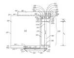
- FIG. 3is a top view of a slider with integrated TAR head and integrated external-cavity VCSEL according to one embodiment of the invention wherein the carrier is attached to the front end of the slider and an optical body is attached to the trailing end of the slider.
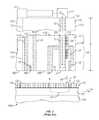
- FIG. 4is a sectional view along a plane through the length of the slider showing the attachment of the optical body to the slider trailing end and the alignment of the laser radiation beam orthogonal to the slider trailing end for the embodiment of FIG. 3 .
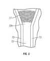
- FIG. 5is a view of the grating coupler and waveguide portion according to the invention as viewed from a direction orthogonal to the slider trailing end.
- FIG. 6Ais a top view of a slider with integrated TAR head and integrated external-cavity VCSEL according to another embodiment of the invention wherein the optical body attached to the slider trailing end has only a single reflective surface.
- FIG. 6Bis an end view of the slider and attached optical body for the embodiment of FIG. 6A and illustrates the grating coupler and optical body attachment being near a side of the slider.
- FIG. 1is a sectional view of a monolithic external-cavity VCSEL according to the prior art and as described in U.S. Pat. No. 6,778,582 B1 and in the previously-cited article by J. G. McInerney, et al.
- the external-cavity VCSELhas a semiconductor substrate 10 with front surface 10 a , back surface 10 b and thickness L.
- a VCSEL with active region 1is formed on front surface 10 a and includes gain layer 16 located between partially reflecting intermediate Bragg reflector or mirror 14 and bottom Bragg mirror 18 , and an oxide layer 22 that defines an aperture 22 a .
- a partially reflecting output mirror 28is formed on the back surface 10 b of semiconductor substrate 10 and functions as a third mirror.
- the laser radiationis emitted through the third mirror 28 .
- the semiconductor substrate 10 with thickness Lfunctions as an external cavity for the VCSEL.
- the external cavityallows for higher single mode power than can be achieved with a typical VCSEL without the external cavity and third mirror.
- the external cavityis made from GaAs, the external-cavity VCSEL may be designed to generate laser radiation with a wavelength of greater than approximately 920 nm. For example, the wavelength may be between 920 nm and 1000 nm. Shorter wavelengths require the use of a different substrate due to optical losses in the in GaAs.
- FIG. 1is a single device that has been cut from a semiconductor wafer onto which the materials making up the various layers have been deposited and patterned using well-known semiconductor lithographic and fabrication processes. Thus a large number of devices are formed on a single wafer.
- the materials, dimensions and fabrication methods for the external-cavity VCSEL shown in FIG. 1are described in detail in U.S. Pat. No. 6,778,582 B1.
- FIG. 2is a sectional view through a portion of a TAR disk 100 and air-bearing slider 110 that functions as the head carrier with integrated TAR head, as proposed in the prior art.
- FIG. 2is not drawn to scale because of the difficulty in showing the very small features.
- the TAR disk 100is depicted as a patterned-media disk with a disk substrate 118 and discrete magnetic islands 130 and nonmagnetic regions 132 .
- the islands 130are spaced apart by nonmagnetic regions 132 , which may formed of polymeric material for planarizing disk 100 .
- the islands 130are magnetized perpendicularly, resulting in the recorded bits being stored in the recording layer of the islands 130 in a generally perpendicular or out-of-plane orientation.
- the islands 130are discrete magnetic islands that function as the patterned bits.
- a heat sink layer 121may be located below the islands 130 and nonmagnetic regions 132 .
- the TAR disk 100may also be a conventional continuous-media magnetic recording disk wherein the recording layer is not patterned but is a continuous layer.
- ABSdisk-facing surface or air-bearing surface
- the ABS of slider 110is the surface that faces the disk 100 and is shown without the thin protective overcoat typically present in an actual slider.
- the ABSshall mean the surface of the head carrier that is covered with a thin protective overcoat, the actual outer surface of the head carrier if there is no overcoat, or the outer surface of the overcoat.
- Write currentpasses through a coil 56 of the write head 50 to generate a magnetic field (arrow 42 ) at the write pole 52 .
- This magnetic fieldmagnetizes the recording layer on the island 130 beneath the write pole 52 as the disk 100 moves past the write head 50 in the direction of arrow 123 .
- the detection or reading of the recorded bitsis by a read head 60 having a sensing edge 60 a at the ABS.
- the read headis typically a magnetoresistive (MR) read head, such as a tunneling MR (TMR) read head in which a sense current passes perpendicularly through the layers making up the head.
- MRmagnetoresistive
- TMRtunneling MR
- a pair of magnetic permeable shields S 1 and S 2are located on opposite sides of read head 60 to prevent magnetic flux from bits other than the bit being read from reaching the read head 60 .
- the write coil 56is shown as a conventional flat or “pancake” coil wrapped around the yoke that connects the write pole 52 with the return pole 54 , with the electrical current directions being shown as into the paper by the coil cross-sections marked with an “X” and out of the paper by the coil cross-sections marked with a solid circle.
- the coilmay also be a conventional helical coil wrapped around the portion of the yoke that directly supports the write pole 52 .
- the slider 110 with integrated TAR headhas an outer surface or trailing end 115 with electrically conductive pads (not shown) that connect through the insulating layers 113 to the read head 60 and coil 56 of write head 50 .
- the slider 110also supports a laser 70 , mirror 71 , optical channel or waveguide 72 and near-field transducer (NFT) 74 , which has its output at the ABS.
- the laser 70 and mirror 71are shown as being supported on the top surface 150 of slider 110 .
- the spacing between the generally parallel ABS and top surface 150defines the height H of the slider 110 , which for conventional sliders is in the range of about 180 to 300 ⁇ m.
- the optical waveguide 72is depicted in FIG. 2 as extending through the yoke of write head 50 and being located between the write pole 52 and return pole 54 . However the optical waveguide 72 may be located at other locations, such as between shield S 2 and return pole 54 , or between the write pole 52 and the outer face of the slider 110 .
- the waveguide 72is formed of a core material such as Ta 2 O 5 or another high index dielectric material that is transmissive to radiation at the wavelength of the laser and is surrounded by a dielectric cladding layer 73 (for example SiO 2 or Al 2 O 3 ) of lower refractive index than the core material. While the slider 110 in FIG. 2 is depicted as supporting mirror 71 for directing the laser radiation from laser 70 into waveguide 72 , it is known to use a grating coupler coupled to the waveguide, as described for example in U.S. 20090310459 A1.
- the NFT 74is located at the output of waveguide 72 at the ABS of the slider 110 .
- the laser radiationstrikes the NFT 74 , creating concentrated near-field radiation to the islands 130 as the disk rotates in the direction 123 past the slider 110 .
- a “near-field” transducerrefers to “near-field optics”, wherein the passage of light is to, from, through, or near an element with subwavelength features and the light is coupled to a second element located a subwavelength distance from the first.
- NFTstypically use a low-loss metal (e.g., Au, Ag, Al or Cu) shaped in such a way to concentrate surface charge motion at a surface feature shaped as a primary apex or tip.
- Oscillating tip chargecreates an intense near-field pattern.
- the metal structurecan create resonant charge motion, called surface plasmons or local plasmons, to further increase intensity.
- the electromagnetic field of the oscillating tip chargethen gives rise to optical output in the near field, which is directed to the data islands on the disk.
- the NFT 74has features less than the wavelength of the laser radiation and the spacing between the NFT 74 and the islands is less than the wavelength of the laser radiation.
- the write pole 52When write-current is directed through coil 56 , the write pole 52 directs magnetic flux to the data islands 130 .
- the dashed line 117 with arrowsshows the flux return path back to the return pole 54 .
- the NFT 74directs near-field radiation, as represented by wavy arrow 82 , to the data islands 130 as the TAR disk 100 moves in the direction 123 relative to the slider 110 .
- the electric charge oscillations in the NFT 74heat the data islands 130 . This raises the temperature of the magnetic recording material in a data island to near or above its Curie temperature to thereby lower the coercivity of the material and enable the magnetization of the data island to be switched by the write field from the write pole 52 .
- the TAR head elementsi.e., read head 60 , shields S 1 , S 2 , return pole 54 , write pole 52 , coil 56 and waveguide 72 , are fabricated on a trailing surface 112 of slider 110 using well-known conventional thin film deposition and patterning techniques.
- the TAR headis thus integrated with the slider 110 , with resulting trailing end 115 .
- Insulating materialtypically alumina, is deposited at various times during the fabrication process to separate the various TAR head elements and refill recessed areas, as shown by insulating layers 113 .
- the insulating materialgenerally surrounds the TAR head elements and provides a portion of the ABS.
- the slider 110is typically formed of an alumina/titanium-carbide (Al 2 O 3 /TiC) composite material.
- the trailing surface 112is the surface of a wafer onto which a large number of TAR heads are patterned. The wafer is then diced into individual sliders with the length of the sliders (in the direction perpendicular to trailing surface 112 ) corresponding generally to the thickness of the wafer.
- US 20090258186 A1assigned to the same assignee as this application, describes a wafer-level process for fabricating TAR heads with thin film waveguides and NFTs.
- the inventionis a slider with integrated TAR head and an integrated relatively long (greater than 300 ⁇ m) laser diode.
- the laser diodeis an external-cavity VCSEL.
- An embodiment of the inventionis shown in the top view of FIG. 3 .
- the slider 210 with integrated TAR headhas a top surface 250 , a front end 225 , a trailing end 215 , and generally parallel sides 260 , 265 .
- the sliderhas a typical length between front end 225 and trailing end 215 of about 850 to 1250 ⁇ m.
- the TAR headis depicted as being integrated with the slider 210 and formed between trailing surface 212 and trailing end 215 .
- the TAR headincludes a grating coupler 77 , which is located in a plane generally parallel to trailing end 215 and is thus depicted in edge view.
- the external-cavity VCSEL 300is attached to carrier 400 which is attached to the front end 225 of slider 210 .
- the external-cavity VCSEL 300is mounted to carrier 400 so that it is located along a side 265 of slider 210 with its laser radiation beam 350 in the direction from the slider front end 225 toward the slider trailing end 215 .
- a solid optical body 500 of radiation-transparent materialis attached to the slider 210 and directs the laser radiation from the external-cavity VCSEL 300 to the grating coupler 77 .
- the external-cavity VCSEL 300includes semiconductor substrate 310 having generally parallel first and second surfaces 310 a , 310 b .
- the semiconductor substrate 310may be formed of GaAs or AlGaAs.
- the first surface 310 ahas deposited on it in succession first Bragg mirror 314 , gain layer 316 , dielectric layer 322 with aperture 322 a , and second Bragg mirror 318 .
- An annular isolation trench 323separates second mirror 318 from the semiconductor substrate 310 .
- a first electrode layer 324 aprovides electrical contact with second mirror 318 and a second electrode layer 324 b provides electrical contact with semiconductor substrate 310 .
- the electrodes 324 a , 324 ballow electrical current to flow through the aperture 322 a .
- the second surface 310 b of semiconductor substrate 310has a block of material 330 attached.
- the material 330may be glass or another material transparent to the laser radiation, such as plastic, and may be attached to surface 310 b by a conventional adhesive, such as epoxy glue.
- the third mirror 328 for the external-cavity VCSEL 300is formed on the output side of material 330 opposite to the side attached to semiconductor substrate surface 310 b .
- the semiconductor substrate 310has a thickness T S and the block of material 330 has a length L 0 .
- the semiconductor substrate 310may have a thickness of L 0 so that the semiconductor substrate 310 alone functions as the external cavity, in the manner as shown in FIG. 1 .
- the semiconductor substrate 310 alone or together with material 330may have a total length L 1 in the range of about 300 to 1500 ⁇ m.
- the carrier 400is attached to the front end 225 of slider 210 , preferably by a layer of adhesive 401 like epoxy, and supports the laser diode.
- the carrier 400is attached at the first surface 310 a of the semiconductor substrate 310 .
- the carrier 400may be formed of various materials, including silicon, aluminum nitride ceramic, or beryllium oxide, and fabricated by known microfabrication processes or by conventional machining.
- the carrier 400has electrically conductive contact pads 405 a , 405 b that connect with contact pads 325 a , 325 b connected to electrodes 324 a , 324 b , respectively, of the external-cavity VCSEL 300 , preferably by reflow solder joints 406 , 408 .
- the electrically conductive contact pads 405 a , 405 bare connected to respective electrically conductive contact pads 407 , 409 on the top surface 402 of carrier 400 .
- the top surface 250 of the slider 210is attached to a flexure/suspension assembly (not shown) which has electrical leads that connect to the contact pads 407 , 409 and thus allow for electrical connection with the laser diode power supply.
- the attachment of the external-cavity VCSEL 300 to carrier 400 by solder reflow joints 406 , 408provides for heat sinking from the external-cavity VCSEL 300 through the contact pads 405 a , 405 b to the carrier 400 and back to the front end 225 of slider 210. This prevents heating of the write head and read head, which are located at the trailing end 225 of slider 210.
- the body 500is depicted with its input surface input surface 510 being generally parallel to output mirror 328 and thus orthogonal to the laser radiation beam 350 . However, the body input surface 510 may make an angle with the laser beam 350 to prevent refection back into the external-cavity VCSEL 300 .
- the body 500is attached to the trailing end 215 of slider 210 , preferably by a layer of adhesive 501 like epoxy, and has an output surface 520 generally parallel to the trailing end 215 of slider 210 and two reflective surfaces 512 and 514 .
- Each reflective surface 512 , 514may be a collimator mirror of reflective material, like gold or aluminum, patterned on the outer surface of body 500 .
- Reflective surface 512turns the radiation from a direction generally parallel to a side 265 of slider 210 to a direction generally parallel to the trailing end 215
- reflective surface 514turns the radiation from a direction generally parallel to the trailing end 215 to a direction generally orthogonal to the trailing end 215 .
- the laser radiationis then directed to output surface 520 and then to grating coupler 77 .
- FIG. 4is a sectional view along a plane through the length of slider 210 showing the attachment of body 500 by a layer of adhesive 501 to the slider trailing end 215 and the alignment of the laser radiation beam orthogonal to the slider trailing end 215 .
- Dashed lines 210 a , 210 brepresent extensions of the slider planes corresponding to the slider top surface 250 and bottom surface (ABS), respectively.
- the carrier 400 ( FIG. 3 ), the attached external-cavity VCSEL 300 ( FIG. 3 ), and the body 500are all located preferably within the region bounded by the two planes 210 a , 210 b .
- the attached external-cavity VCSEL 300 and the body 500may extend slightly above line 210 a if allowed by the design of the suspension that attaches to the top surface 250 of slider 210 , for example by providing a hole in the suspension to allow for the slight extension.
- the carrier 400 , attached external-cavity VCSEL 300 , and optical body 500do not substantially increase the overall height H of the slider, so there is no need to increase the disk-to-disk spacing of the disk drive.
- the laser radiation beam 350 output from output surface 520has a generally linear path that is depicted as being substantially orthogonal to slider trailing end 215 .
- the laser beam 350does not have to be orthogonal to slider trailing end 215 , but can make a small angle, which may make the design of coupler 77 easier, as described by Van Laere et al., “Compact Focusing Grating Couplers Between Optical Fibers and Silicon-on-Insulator Photonic Wire Waveguides”, Optical Fiber Communication and the National Fiber Optic Engineers Conference on 25-29 March 2007.
- the laser beam 350travels through insulating layer 113 to grating coupler 77 that lies in a plane generally parallel to trailing end 215 .
- the insulating material 113is transparent to the laser radiation, which may have a wavelength between about 920 and 1000 nm.
- the grating coupler 77turns the incoming laser radiation and directs it into waveguide 72 , which is located between cladding layers 73 .
- the waveguide 72directs the laser radiation to NFT 74 at the ABS.
- FIG. 5is a view of grating coupler 77 and shows the tapered input end 72 a of waveguide 72 as viewed from a direction orthogonal to trailing end 215 .
- the grating coupler 77is coupled to the tapered end 72 a of waveguide 72 , which is located between cladding layers 73 .
- Grating couplersare well-known and have been proposed for use in TAR heads, as described for example in U.S. 20090310459 A1. Focusing grating couplers and grating couplers coupled to tapered waveguides are described by Van Laere, et al., “Compact Focusing Grating Couplers for Silicon-on-Insulator Integrated Circuits”, IEEE PHOTONICS TECHNOLOGY LETTERS , VOL.19, NO. 23, Dec. 1, 2007, pp. 1919-1921.
- FIG. 6Ais a top view of a slider with integrated TAR head and integrated external-cavity VCSEL according to another embodiment of the invention wherein the optical body 600 has input and output surfaces 610 , 620 , respectively, but only a single reflective surface 612 .
- the external-cavity VCSEL 300is identical to that shown and described in FIG. 3 , so not all details are illustrated.
- the reflective surface 612is located in a plane that makes an angle with the incoming laser radiation beam 350 from output mirror 328 so that it is directed from a direction generally parallel to the side 265 of slider 210 to output surface 620 and then through insulating layer 113 to grating coupler 77 .
- the radiation beam 350is depicted as being generally orthogonal to input surface 610 , but input surface 610 may be oriented to be non-orthogonal to radiation beam 350 to prevent refection back to the external cavity VCSEL.
- the radiation beam 350enters trailing end 215 at a non-orthogonal angle.
- the grating coupler 77is offset from the midline between slider edges 260 , 265 , but the waveguide 72 (shown in dotted lines) to which it is coupled is angled downward toward the midline to NFT 74 , which is located at the midline at the slider ABS.
- FIG. 6Bis an end view of the slider 210 and attached optical body 600 and illustrates the advantage that the grating coupler 77 and the attachment of optical body 600 are located near a side 265 of the slider 210 away from the write head 50 and read head.
- FIG. 6Balso illustrates that, like the embodiment of FIG. 3 , the carrier 400 , attached external-cavity VCSEL 300 , and optical body 600 do not increase the overall height H of the slider, so there is no need to increase the disk-to-disk spacing of the disk drive.
Landscapes
- Engineering & Computer Science (AREA)
- Manufacturing & Machinery (AREA)
- Physics & Mathematics (AREA)
- Electromagnetism (AREA)
- Recording Or Reproducing By Magnetic Means (AREA)
- Optical Head (AREA)
- Adjustment Of The Magnetic Head Position Track Following On Tapes (AREA)
Abstract
Description
Claims (26)
Priority Applications (1)
| Application Number | Priority Date | Filing Date | Title |
|---|---|---|---|
| US12/969,307US8184507B1 (en) | 2010-12-15 | 2010-12-15 | Slider with integrated thermally-assisted recording (TAR) head and long laser diode with optical body for directing laser radiation |
Applications Claiming Priority (1)
| Application Number | Priority Date | Filing Date | Title |
|---|---|---|---|
| US12/969,307US8184507B1 (en) | 2010-12-15 | 2010-12-15 | Slider with integrated thermally-assisted recording (TAR) head and long laser diode with optical body for directing laser radiation |
Publications (1)
| Publication Number | Publication Date |
|---|---|
| US8184507B1true US8184507B1 (en) | 2012-05-22 |
Family
ID=46061287
Family Applications (1)
| Application Number | Title | Priority Date | Filing Date |
|---|---|---|---|
| US12/969,307ActiveUS8184507B1 (en) | 2010-12-15 | 2010-12-15 | Slider with integrated thermally-assisted recording (TAR) head and long laser diode with optical body for directing laser radiation |
Country Status (1)
| Country | Link |
|---|---|
| US (1) | US8184507B1 (en) |
Cited By (11)
| Publication number | Priority date | Publication date | Assignee | Title |
|---|---|---|---|---|
| US20110267930A1 (en)* | 2010-04-30 | 2011-11-03 | Seagate Technology Llc | Method and Apparatus for Aligning a Laser Diode on a Slider |
| US20120327752A1 (en)* | 2011-06-23 | 2012-12-27 | Seagate Technology Llc | Transducer Bonded To A Laser Module For Heat Assisted Magnetic Recording |
| US20120327754A1 (en)* | 2011-06-23 | 2012-12-27 | Seagate Technology Llc | Vertical Cavity Surface Emitting Laser With Integrated Mirror And Waveguide |
| US20140168632A1 (en)* | 2012-12-19 | 2014-06-19 | Robert Bosch Gmbh | Measuring Apparatus and Referencing Method for a Digital Laser Distance Meter, and Laser Distance Meter |
| US8837261B1 (en) | 2013-08-27 | 2014-09-16 | HGST Netherlands B.V. | Electrical contact for an energy-assisted magnetic recording laser sub-mount |
| US8923102B1 (en) | 2013-07-16 | 2014-12-30 | Western Digital (Fremont), Llc | Optical grating coupling for interferometric waveguides in heat assisted magnetic recording heads |
| US20150069113A1 (en)* | 2013-09-11 | 2015-03-12 | Princeton Optronics Inc. | VCSEL Packaging |
| US9065236B2 (en) | 2010-04-30 | 2015-06-23 | Seagate Technology | Method and apparatus for aligning a laser diode on a slider |
| US9129634B1 (en)* | 2014-06-17 | 2015-09-08 | HGST Netherlands B.V. | Integrated compound DBR laser for HAMR applications |
| US20220407288A1 (en)* | 2021-06-16 | 2022-12-22 | Western Digital Technologies, Inc. | Vertical cavity surface emitting laser, head gimbal assembly, and fabrication process |
| US11867956B2 (en)* | 2021-08-19 | 2024-01-09 | Advanced Semiconductor Engineering, Inc. | Optoelectronic device |
Citations (20)
| Publication number | Priority date | Publication date | Assignee | Title |
|---|---|---|---|---|
| US6404706B1 (en) | 1999-02-12 | 2002-06-11 | Read-Rite Corporation | Laser mounting for a thermally assisted GMR head |
| US20030007442A1 (en) | 2001-07-09 | 2003-01-09 | Henrichs Joseph Reid | Light intensity modulated direct overwrite magneto-optical microhead array chip hard disk drive |
| US6549506B1 (en) | 2000-07-17 | 2003-04-15 | Iomega Corporation | Photo detector mounting in a head gimbal assembly used in an optical data storage device |
| US6614827B1 (en) | 1997-03-21 | 2003-09-02 | Novalux, Inc. | High power laser |
| US6771589B2 (en) | 2000-05-10 | 2004-08-03 | Fuji Xerox Co., Ltd. | Flying recording head having semiconductor laser formed by growing semiconductor crystal, and method of manufacturing same |
| US6778582B1 (en) | 2000-03-06 | 2004-08-17 | Novalux, Inc. | Coupled cavity high power semiconductor laser |
| US20050226304A1 (en) | 2004-01-30 | 2005-10-13 | Osram Opto Semiconductors Gmbh | Surface emitting semiconductor laser having an interference filter |
| US20060187564A1 (en) | 2004-12-28 | 2006-08-24 | Tdk Corporation | Heat assisted magnetic recording head and heat assisted magnetic recording apparatus |
| US7133230B2 (en) | 2002-11-05 | 2006-11-07 | Hitachi, Ltd. | Recording head and information recording apparatus |
| US20080002298A1 (en) | 2006-06-30 | 2008-01-03 | Seagate Technology Llc | Optoelectronic emitter mounted on a slider |
| US20080316872A1 (en) | 2007-06-21 | 2008-12-25 | Junichiro Shimizu | Optical device integrated head |
| US20090196128A1 (en) | 2008-01-31 | 2009-08-06 | Lille Jeffrey S | Thermally assisted recording systems with low loss light redirection structure |
| JP2009277285A (en) | 2008-05-14 | 2009-11-26 | Konica Minolta Opto Inc | Head mechanism, optical assist type magnetic recording device, and optical recording device |
| US20090310459A1 (en) | 2008-06-12 | 2009-12-17 | Seagate Technology Llc | Laser On Slider For A Heat Assisted Magnetic Recording Head |
| JP2009301597A (en) | 2008-06-10 | 2009-12-24 | Hitachi Ltd | Thermally-assisted magnetic recording head |
| US20100002332A1 (en) | 2002-06-19 | 2010-01-07 | Dugas Matthew P | Optical Path for a Thermal-Assisted Magnetic Recording Head |
| US20100007980A1 (en) | 2006-05-17 | 2010-01-14 | Samsung Electronics Co., Ltd. | Heat-assisted magnetic recording head gimbal assembly |
| JP2010027185A (en) | 2008-07-24 | 2010-02-04 | Toshiba Storage Device Corp | Head gimbal assembly and information storage device |
| US20100165801A1 (en)* | 2008-12-31 | 2010-07-01 | Hitachi Global Storage Technologies Netherlands Bv | System, method and apparatus for internal polarization rotation for horizontal cavity, surface emitting laser beam for thermally assisted recording in disk drive |
| US20120008233A1 (en)* | 2010-07-09 | 2012-01-12 | Hitachi Global Storage Technologies Netherlands B.V. | Extended Cavity VCSEL Mounted to Substrate with Electrical and Thermal Contact to Substrate and Optical Power Directed Toward Substrate |
- 2010
- 2010-12-15USUS12/969,307patent/US8184507B1/enactiveActive
Patent Citations (21)
| Publication number | Priority date | Publication date | Assignee | Title |
|---|---|---|---|---|
| US6614827B1 (en) | 1997-03-21 | 2003-09-02 | Novalux, Inc. | High power laser |
| US6404706B1 (en) | 1999-02-12 | 2002-06-11 | Read-Rite Corporation | Laser mounting for a thermally assisted GMR head |
| US6778582B1 (en) | 2000-03-06 | 2004-08-17 | Novalux, Inc. | Coupled cavity high power semiconductor laser |
| US6771589B2 (en) | 2000-05-10 | 2004-08-03 | Fuji Xerox Co., Ltd. | Flying recording head having semiconductor laser formed by growing semiconductor crystal, and method of manufacturing same |
| US6549506B1 (en) | 2000-07-17 | 2003-04-15 | Iomega Corporation | Photo detector mounting in a head gimbal assembly used in an optical data storage device |
| US20030007442A1 (en) | 2001-07-09 | 2003-01-09 | Henrichs Joseph Reid | Light intensity modulated direct overwrite magneto-optical microhead array chip hard disk drive |
| US20100002332A1 (en) | 2002-06-19 | 2010-01-07 | Dugas Matthew P | Optical Path for a Thermal-Assisted Magnetic Recording Head |
| US7133230B2 (en) | 2002-11-05 | 2006-11-07 | Hitachi, Ltd. | Recording head and information recording apparatus |
| US20050226304A1 (en) | 2004-01-30 | 2005-10-13 | Osram Opto Semiconductors Gmbh | Surface emitting semiconductor laser having an interference filter |
| US20060187564A1 (en) | 2004-12-28 | 2006-08-24 | Tdk Corporation | Heat assisted magnetic recording head and heat assisted magnetic recording apparatus |
| US20100007980A1 (en) | 2006-05-17 | 2010-01-14 | Samsung Electronics Co., Ltd. | Heat-assisted magnetic recording head gimbal assembly |
| US7643248B2 (en) | 2006-06-30 | 2010-01-05 | Seagate Technology Llc | Optoelectronic emitter mounted on a slider |
| US20080002298A1 (en) | 2006-06-30 | 2008-01-03 | Seagate Technology Llc | Optoelectronic emitter mounted on a slider |
| US20080316872A1 (en) | 2007-06-21 | 2008-12-25 | Junichiro Shimizu | Optical device integrated head |
| US20090196128A1 (en) | 2008-01-31 | 2009-08-06 | Lille Jeffrey S | Thermally assisted recording systems with low loss light redirection structure |
| JP2009277285A (en) | 2008-05-14 | 2009-11-26 | Konica Minolta Opto Inc | Head mechanism, optical assist type magnetic recording device, and optical recording device |
| JP2009301597A (en) | 2008-06-10 | 2009-12-24 | Hitachi Ltd | Thermally-assisted magnetic recording head |
| US20090310459A1 (en) | 2008-06-12 | 2009-12-17 | Seagate Technology Llc | Laser On Slider For A Heat Assisted Magnetic Recording Head |
| JP2010027185A (en) | 2008-07-24 | 2010-02-04 | Toshiba Storage Device Corp | Head gimbal assembly and information storage device |
| US20100165801A1 (en)* | 2008-12-31 | 2010-07-01 | Hitachi Global Storage Technologies Netherlands Bv | System, method and apparatus for internal polarization rotation for horizontal cavity, surface emitting laser beam for thermally assisted recording in disk drive |
| US20120008233A1 (en)* | 2010-07-09 | 2012-01-12 | Hitachi Global Storage Technologies Netherlands B.V. | Extended Cavity VCSEL Mounted to Substrate with Electrical and Thermal Contact to Substrate and Optical Power Directed Toward Substrate |
Non-Patent Citations (5)
| Title |
|---|
| "Thermally Assisted Recording Head with heat source on side of slider and method for producing the same", published on web at http://ip.com/IPCOM/000157835, Sep. 5, 2007. |
| Hadley, et al., "High single-transverse-mode output from external-cavity surface-emitting laser diodes", Appl. Phys. Lett. 63 (12), Sep. 20, 1993, pp. 1607-1609. |
| J. G. McInerney, et al., "High brightness 980 nm pump lasers based on the Novalux Extended Cavity Surface-Emitting Laser (NECSEL) concept", Proc. of SPIE vol. 4947 (2003), pp. 240 251. |
| Van Laere et al., "Compact Focusing Grating Couplers Between Optical Fibers and Silicon-on-Insulator Photonic Wire Waveguides", Optical Fiber Communication and the National Fiber Optic Engineers Conference on Mar. 25-29, 2007. |
| Van Laere, et al., "Compact Focusing Grating Couplers for Silicon-on-Insulator Integrated Circuits", IEEE Photonics Technology Letters, vol. 19, No. 23, Dec. 1, 2007, pp. 1919-1921. |
Cited By (19)
| Publication number | Priority date | Publication date | Assignee | Title |
|---|---|---|---|---|
| US20110267930A1 (en)* | 2010-04-30 | 2011-11-03 | Seagate Technology Llc | Method and Apparatus for Aligning a Laser Diode on a Slider |
| US9489967B2 (en) | 2010-04-30 | 2016-11-08 | Seagate Technology Llc | Method and apparatus for aligning a laser diode on a slider |
| US9065236B2 (en) | 2010-04-30 | 2015-06-23 | Seagate Technology | Method and apparatus for aligning a laser diode on a slider |
| US8345517B2 (en)* | 2010-04-30 | 2013-01-01 | Seagate Technology Llc | Method and apparatus for aligning a laser diode on a slider |
| US8451695B2 (en)* | 2011-06-23 | 2013-05-28 | Seagate Technology Llc | Vertical cavity surface emitting laser with integrated mirror and waveguide |
| US20120327752A1 (en)* | 2011-06-23 | 2012-12-27 | Seagate Technology Llc | Transducer Bonded To A Laser Module For Heat Assisted Magnetic Recording |
| US8488435B2 (en)* | 2011-06-23 | 2013-07-16 | Seagate Technology Llc | Transducer bonded to a laser module for heat assisted magnetic recording |
| US20120327754A1 (en)* | 2011-06-23 | 2012-12-27 | Seagate Technology Llc | Vertical Cavity Surface Emitting Laser With Integrated Mirror And Waveguide |
| US9041918B2 (en)* | 2012-12-19 | 2015-05-26 | Robert Bosch Gmbh | Measuring apparatus and referencing method for a digital laser distance meter, and laser distance meter |
| US20140168632A1 (en)* | 2012-12-19 | 2014-06-19 | Robert Bosch Gmbh | Measuring Apparatus and Referencing Method for a Digital Laser Distance Meter, and Laser Distance Meter |
| US8923102B1 (en) | 2013-07-16 | 2014-12-30 | Western Digital (Fremont), Llc | Optical grating coupling for interferometric waveguides in heat assisted magnetic recording heads |
| US8837261B1 (en) | 2013-08-27 | 2014-09-16 | HGST Netherlands B.V. | Electrical contact for an energy-assisted magnetic recording laser sub-mount |
| US9038883B2 (en)* | 2013-09-11 | 2015-05-26 | Princeton Optronics Inc. | VCSEL packaging |
| US20150069113A1 (en)* | 2013-09-11 | 2015-03-12 | Princeton Optronics Inc. | VCSEL Packaging |
| US9129634B1 (en)* | 2014-06-17 | 2015-09-08 | HGST Netherlands B.V. | Integrated compound DBR laser for HAMR applications |
| US20220407288A1 (en)* | 2021-06-16 | 2022-12-22 | Western Digital Technologies, Inc. | Vertical cavity surface emitting laser, head gimbal assembly, and fabrication process |
| WO2022266001A1 (en)* | 2021-06-16 | 2022-12-22 | Western Digital Technologies, Inc. | Vertical cavity surface emitting laser, head gimbal assembly, and fabrication process |
| US11817677B2 (en)* | 2021-06-16 | 2023-11-14 | Western Digital Technologies, Inc. | Vertical cavity surface emitting laser, head gimbal assembly, and fabrication process |
| US11867956B2 (en)* | 2021-08-19 | 2024-01-09 | Advanced Semiconductor Engineering, Inc. | Optoelectronic device |
Similar Documents
| Publication | Publication Date | Title |
|---|---|---|
| US8107326B1 (en) | Slider with integrated thermally-assisted recording (TAR) head and integrated long laser diode | |
| US8184507B1 (en) | Slider with integrated thermally-assisted recording (TAR) head and long laser diode with optical body for directing laser radiation | |
| US8194512B2 (en) | Head structure for thermally-assisted recording (TAR) disk drive | |
| JP5668965B2 (en) | Thermally assisted magnetic recording device and method for making an integrated thermally assisted magnetic recording device | |
| US8102736B2 (en) | Near-field light generator comprising waveguide with inclined end surface | |
| JP5528832B2 (en) | Thermally assisted magnetic recording head with laser diode fixed to slider | |
| JP5008101B2 (en) | Thermally assisted magnetic recording head with converging lens | |
| US8116171B1 (en) | Method and system for providing energy assisted magnetic recording disk drive using a vertical surface emitting laser | |
| US8422342B1 (en) | Energy assisted magnetic recording disk drive using a distributed feedback laser | |
| US8495813B1 (en) | Method of making an energy-assisted magnetic recording apparatus | |
| CN101329872B (en) | Optical element integrated head | |
| US8406089B2 (en) | Heat-assisted magnetic recording head with laser diode fixed to slider | |
| US8395972B2 (en) | Thermally assisted magnetic head, head gimbal assembly, and hard disk drive | |
| US8139448B1 (en) | Slider with integrated thermally-assisted recording (TAR) head and vertical-cavity surface-emitting laser (VCSEL) with angled external cavity | |
| US8107192B2 (en) | Heat-assisted magnetic recording head with laser diode fixed to slider | |
| US8223596B2 (en) | Thermally-assisted magnetic recording head with plane-emission type light source | |
| JP2008059645A (en) | Recording head | |
| JP2010040112A (en) | Heat-assisted magnetic recording head | |
| US9431043B2 (en) | Integrated compound DBR laser for HAMR applications | |
| US10734019B1 (en) | Curved-edge optical mode converter for heat-assisted magnetic recording | |
| US10971179B1 (en) | Compact mode converter having first and second straight portions for a heat-assisted magnetic recording device | |
| JP5379759B2 (en) | Thermally assisted integrated head and thermally assisted recording device | |
| US12345915B1 (en) | Heterogeneous integration of active layers on a heat-assisted magnetic recording slider |
Legal Events
| Date | Code | Title | Description |
|---|---|---|---|
| AS | Assignment | Owner name:HITACHI GLOBAL STORAGE TECHNOLOGIES NETHERLANDS B. Free format text:ASSIGNMENT OF ASSIGNORS INTEREST;ASSIGNORS:HIRANO, TOSHIKI;STIPE, BARRY CUSHING;STRAND, TIMOTHY CARL;SIGNING DATES FROM 20101206 TO 20101214;REEL/FRAME:025507/0427 | |
| FEPP | Fee payment procedure | Free format text:PAYOR NUMBER ASSIGNED (ORIGINAL EVENT CODE: ASPN); ENTITY STATUS OF PATENT OWNER: LARGE ENTITY | |
| STCF | Information on status: patent grant | Free format text:PATENTED CASE | |
| AS | Assignment | Owner name:HGST, NETHERLANDS B.V., NETHERLANDS Free format text:CHANGE OF NAME;ASSIGNOR:HGST, NETHERLANDS B.V.;REEL/FRAME:029341/0777 Effective date:20120723 Owner name:HGST NETHERLANDS B.V., NETHERLANDS Free format text:CHANGE OF NAME;ASSIGNOR:HITACHI GLOBAL STORAGE TECHNOLOGIES NETHERLANDS B.V.;REEL/FRAME:029341/0777 Effective date:20120723 | |
| FPAY | Fee payment | Year of fee payment:4 | |
| AS | Assignment | Owner name:WESTERN DIGITAL TECHNOLOGIES, INC., CALIFORNIA Free format text:ASSIGNMENT OF ASSIGNORS INTEREST;ASSIGNOR:HGST NETHERLANDS B.V.;REEL/FRAME:040826/0327 Effective date:20160831 | |
| MAFP | Maintenance fee payment | Free format text:PAYMENT OF MAINTENANCE FEE, 8TH YEAR, LARGE ENTITY (ORIGINAL EVENT CODE: M1552); ENTITY STATUS OF PATENT OWNER: LARGE ENTITY Year of fee payment:8 | |
| AS | Assignment | Owner name:JPMORGAN CHASE BANK, N.A., AS AGENT, ILLINOIS Free format text:SECURITY INTEREST;ASSIGNOR:WESTERN DIGITAL TECHNOLOGIES, INC.;REEL/FRAME:052915/0566 Effective date:20200113 | |
| AS | Assignment | Owner name:WESTERN DIGITAL TECHNOLOGIES, INC., CALIFORNIA Free format text:RELEASE OF SECURITY INTEREST AT REEL 052915 FRAME 0566;ASSIGNOR:JPMORGAN CHASE BANK, N.A.;REEL/FRAME:059127/0001 Effective date:20220203 | |
| AS | Assignment | Owner name:JPMORGAN CHASE BANK, N.A., ILLINOIS Free format text:PATENT COLLATERAL AGREEMENT - A&R LOAN AGREEMENT;ASSIGNOR:WESTERN DIGITAL TECHNOLOGIES, INC.;REEL/FRAME:064715/0001 Effective date:20230818 Owner name:JPMORGAN CHASE BANK, N.A., ILLINOIS Free format text:PATENT COLLATERAL AGREEMENT - DDTL LOAN AGREEMENT;ASSIGNOR:WESTERN DIGITAL TECHNOLOGIES, INC.;REEL/FRAME:067045/0156 Effective date:20230818 | |
| MAFP | Maintenance fee payment | Free format text:PAYMENT OF MAINTENANCE FEE, 12TH YEAR, LARGE ENTITY (ORIGINAL EVENT CODE: M1553); ENTITY STATUS OF PATENT OWNER: LARGE ENTITY Year of fee payment:12 |