US8183678B2 - Semiconductor device having an interposer - Google Patents
Semiconductor device having an interposerDownload PDFInfo
- Publication number
- US8183678B2 US8183678B2US12/535,316US53531609AUS8183678B2US 8183678 B2US8183678 B2US 8183678B2US 53531609 AUS53531609 AUS 53531609AUS 8183678 B2US8183678 B2US 8183678B2
- Authority
- US
- United States
- Prior art keywords
- semiconductor die
- interposer
- semiconductor device
- semiconductor
- regions
- Prior art date
- Legal status (The legal status is an assumption and is not a legal conclusion. Google has not performed a legal analysis and makes no representation as to the accuracy of the status listed.)
- Active, expires
Links
Images


Classifications
- H—ELECTRICITY
- H01—ELECTRIC ELEMENTS
- H01L—SEMICONDUCTOR DEVICES NOT COVERED BY CLASS H10
- H01L24/00—Arrangements for connecting or disconnecting semiconductor or solid-state bodies; Methods or apparatus related thereto
- H01L24/80—Methods for connecting semiconductor or other solid state bodies using means for bonding being attached to, or being formed on, the surface to be connected
- H01L24/85—Methods for connecting semiconductor or other solid state bodies using means for bonding being attached to, or being formed on, the surface to be connected using a wire connector
- H—ELECTRICITY
- H01—ELECTRIC ELEMENTS
- H01L—SEMICONDUCTOR DEVICES NOT COVERED BY CLASS H10
- H01L23/00—Details of semiconductor or other solid state devices
- H01L23/48—Arrangements for conducting electric current to or from the solid state body in operation, e.g. leads, terminal arrangements ; Selection of materials therefor
- H01L23/488—Arrangements for conducting electric current to or from the solid state body in operation, e.g. leads, terminal arrangements ; Selection of materials therefor consisting of soldered or bonded constructions
- H01L23/498—Leads, i.e. metallisations or lead-frames on insulating substrates, e.g. chip carriers
- H01L23/49827—Via connections through the substrates, e.g. pins going through the substrate, coaxial cables
- H—ELECTRICITY
- H01—ELECTRIC ELEMENTS
- H01L—SEMICONDUCTOR DEVICES NOT COVERED BY CLASS H10
- H01L23/00—Details of semiconductor or other solid state devices
- H01L23/48—Arrangements for conducting electric current to or from the solid state body in operation, e.g. leads, terminal arrangements ; Selection of materials therefor
- H01L23/488—Arrangements for conducting electric current to or from the solid state body in operation, e.g. leads, terminal arrangements ; Selection of materials therefor consisting of soldered or bonded constructions
- H01L23/498—Leads, i.e. metallisations or lead-frames on insulating substrates, e.g. chip carriers
- H01L23/49833—Leads, i.e. metallisations or lead-frames on insulating substrates, e.g. chip carriers the chip support structure consisting of a plurality of insulating substrates
- H—ELECTRICITY
- H01—ELECTRIC ELEMENTS
- H01L—SEMICONDUCTOR DEVICES NOT COVERED BY CLASS H10
- H01L24/00—Arrangements for connecting or disconnecting semiconductor or solid-state bodies; Methods or apparatus related thereto
- H01L24/73—Means for bonding being of different types provided for in two or more of groups H01L24/10, H01L24/18, H01L24/26, H01L24/34, H01L24/42, H01L24/50, H01L24/63, H01L24/71
- H—ELECTRICITY
- H01—ELECTRIC ELEMENTS
- H01L—SEMICONDUCTOR DEVICES NOT COVERED BY CLASS H10
- H01L25/00—Assemblies consisting of a plurality of semiconductor or other solid state devices
- H01L25/03—Assemblies consisting of a plurality of semiconductor or other solid state devices all the devices being of a type provided for in a single subclass of subclasses H10B, H10D, H10F, H10H, H10K or H10N, e.g. assemblies of rectifier diodes
- H01L25/04—Assemblies consisting of a plurality of semiconductor or other solid state devices all the devices being of a type provided for in a single subclass of subclasses H10B, H10D, H10F, H10H, H10K or H10N, e.g. assemblies of rectifier diodes the devices not having separate containers
- H01L25/065—Assemblies consisting of a plurality of semiconductor or other solid state devices all the devices being of a type provided for in a single subclass of subclasses H10B, H10D, H10F, H10H, H10K or H10N, e.g. assemblies of rectifier diodes the devices not having separate containers the devices being of a type provided for in group H10D89/00
- H01L25/0657—Stacked arrangements of devices
- H—ELECTRICITY
- H01—ELECTRIC ELEMENTS
- H01L—SEMICONDUCTOR DEVICES NOT COVERED BY CLASS H10
- H01L2224/00—Indexing scheme for arrangements for connecting or disconnecting semiconductor or solid-state bodies and methods related thereto as covered by H01L24/00
- H01L2224/01—Means for bonding being attached to, or being formed on, the surface to be connected, e.g. chip-to-package, die-attach, "first-level" interconnects; Manufacturing methods related thereto
- H01L2224/02—Bonding areas; Manufacturing methods related thereto
- H01L2224/04—Structure, shape, material or disposition of the bonding areas prior to the connecting process
- H01L2224/06—Structure, shape, material or disposition of the bonding areas prior to the connecting process of a plurality of bonding areas
- H01L2224/061—Disposition
- H01L2224/0618—Disposition being disposed on at least two different sides of the body, e.g. dual array
- H01L2224/06181—On opposite sides of the body
- H—ELECTRICITY
- H01—ELECTRIC ELEMENTS
- H01L—SEMICONDUCTOR DEVICES NOT COVERED BY CLASS H10
- H01L2224/00—Indexing scheme for arrangements for connecting or disconnecting semiconductor or solid-state bodies and methods related thereto as covered by H01L24/00
- H01L2224/01—Means for bonding being attached to, or being formed on, the surface to be connected, e.g. chip-to-package, die-attach, "first-level" interconnects; Manufacturing methods related thereto
- H01L2224/02—Bonding areas; Manufacturing methods related thereto
- H01L2224/04—Structure, shape, material or disposition of the bonding areas prior to the connecting process
- H01L2224/06—Structure, shape, material or disposition of the bonding areas prior to the connecting process of a plurality of bonding areas
- H01L2224/061—Disposition
- H01L2224/0618—Disposition being disposed on at least two different sides of the body, e.g. dual array
- H01L2224/06183—On contiguous sides of the body
- H—ELECTRICITY
- H01—ELECTRIC ELEMENTS
- H01L—SEMICONDUCTOR DEVICES NOT COVERED BY CLASS H10
- H01L2224/00—Indexing scheme for arrangements for connecting or disconnecting semiconductor or solid-state bodies and methods related thereto as covered by H01L24/00
- H01L2224/01—Means for bonding being attached to, or being formed on, the surface to be connected, e.g. chip-to-package, die-attach, "first-level" interconnects; Manufacturing methods related thereto
- H01L2224/10—Bump connectors; Manufacturing methods related thereto
- H01L2224/12—Structure, shape, material or disposition of the bump connectors prior to the connecting process
- H01L2224/13—Structure, shape, material or disposition of the bump connectors prior to the connecting process of an individual bump connector
- H01L2224/13001—Core members of the bump connector
- H01L2224/1302—Disposition
- H01L2224/13025—Disposition the bump connector being disposed on a via connection of the semiconductor or solid-state body
- H—ELECTRICITY
- H01—ELECTRIC ELEMENTS
- H01L—SEMICONDUCTOR DEVICES NOT COVERED BY CLASS H10
- H01L2224/00—Indexing scheme for arrangements for connecting or disconnecting semiconductor or solid-state bodies and methods related thereto as covered by H01L24/00
- H01L2224/01—Means for bonding being attached to, or being formed on, the surface to be connected, e.g. chip-to-package, die-attach, "first-level" interconnects; Manufacturing methods related thereto
- H01L2224/10—Bump connectors; Manufacturing methods related thereto
- H01L2224/15—Structure, shape, material or disposition of the bump connectors after the connecting process
- H01L2224/16—Structure, shape, material or disposition of the bump connectors after the connecting process of an individual bump connector
- H01L2224/161—Disposition
- H01L2224/16151—Disposition the bump connector connecting between a semiconductor or solid-state body and an item not being a semiconductor or solid-state body, e.g. chip-to-substrate, chip-to-passive
- H01L2224/16221—Disposition the bump connector connecting between a semiconductor or solid-state body and an item not being a semiconductor or solid-state body, e.g. chip-to-substrate, chip-to-passive the body and the item being stacked
- H01L2224/16225—Disposition the bump connector connecting between a semiconductor or solid-state body and an item not being a semiconductor or solid-state body, e.g. chip-to-substrate, chip-to-passive the body and the item being stacked the item being non-metallic, e.g. insulating substrate with or without metallisation
- H01L2224/16227—Disposition the bump connector connecting between a semiconductor or solid-state body and an item not being a semiconductor or solid-state body, e.g. chip-to-substrate, chip-to-passive the body and the item being stacked the item being non-metallic, e.g. insulating substrate with or without metallisation the bump connector connecting to a bond pad of the item
- H—ELECTRICITY
- H01—ELECTRIC ELEMENTS
- H01L—SEMICONDUCTOR DEVICES NOT COVERED BY CLASS H10
- H01L2224/00—Indexing scheme for arrangements for connecting or disconnecting semiconductor or solid-state bodies and methods related thereto as covered by H01L24/00
- H01L2224/01—Means for bonding being attached to, or being formed on, the surface to be connected, e.g. chip-to-package, die-attach, "first-level" interconnects; Manufacturing methods related thereto
- H01L2224/10—Bump connectors; Manufacturing methods related thereto
- H01L2224/15—Structure, shape, material or disposition of the bump connectors after the connecting process
- H01L2224/17—Structure, shape, material or disposition of the bump connectors after the connecting process of a plurality of bump connectors
- H01L2224/171—Disposition
- H01L2224/1718—Disposition being disposed on at least two different sides of the body, e.g. dual array
- H01L2224/17181—On opposite sides of the body
- H—ELECTRICITY
- H01—ELECTRIC ELEMENTS
- H01L—SEMICONDUCTOR DEVICES NOT COVERED BY CLASS H10
- H01L2224/00—Indexing scheme for arrangements for connecting or disconnecting semiconductor or solid-state bodies and methods related thereto as covered by H01L24/00
- H01L2224/01—Means for bonding being attached to, or being formed on, the surface to be connected, e.g. chip-to-package, die-attach, "first-level" interconnects; Manufacturing methods related thereto
- H01L2224/26—Layer connectors, e.g. plate connectors, solder or adhesive layers; Manufacturing methods related thereto
- H01L2224/31—Structure, shape, material or disposition of the layer connectors after the connecting process
- H01L2224/32—Structure, shape, material or disposition of the layer connectors after the connecting process of an individual layer connector
- H01L2224/321—Disposition
- H01L2224/32151—Disposition the layer connector connecting between a semiconductor or solid-state body and an item not being a semiconductor or solid-state body, e.g. chip-to-substrate, chip-to-passive
- H01L2224/32221—Disposition the layer connector connecting between a semiconductor or solid-state body and an item not being a semiconductor or solid-state body, e.g. chip-to-substrate, chip-to-passive the body and the item being stacked
- H01L2224/32225—Disposition the layer connector connecting between a semiconductor or solid-state body and an item not being a semiconductor or solid-state body, e.g. chip-to-substrate, chip-to-passive the body and the item being stacked the item being non-metallic, e.g. insulating substrate with or without metallisation
- H—ELECTRICITY
- H01—ELECTRIC ELEMENTS
- H01L—SEMICONDUCTOR DEVICES NOT COVERED BY CLASS H10
- H01L2224/00—Indexing scheme for arrangements for connecting or disconnecting semiconductor or solid-state bodies and methods related thereto as covered by H01L24/00
- H01L2224/01—Means for bonding being attached to, or being formed on, the surface to be connected, e.g. chip-to-package, die-attach, "first-level" interconnects; Manufacturing methods related thereto
- H01L2224/42—Wire connectors; Manufacturing methods related thereto
- H01L2224/47—Structure, shape, material or disposition of the wire connectors after the connecting process
- H01L2224/48—Structure, shape, material or disposition of the wire connectors after the connecting process of an individual wire connector
- H01L2224/4805—Shape
- H01L2224/4809—Loop shape
- H01L2224/48091—Arched
- H—ELECTRICITY
- H01—ELECTRIC ELEMENTS
- H01L—SEMICONDUCTOR DEVICES NOT COVERED BY CLASS H10
- H01L2224/00—Indexing scheme for arrangements for connecting or disconnecting semiconductor or solid-state bodies and methods related thereto as covered by H01L24/00
- H01L2224/01—Means for bonding being attached to, or being formed on, the surface to be connected, e.g. chip-to-package, die-attach, "first-level" interconnects; Manufacturing methods related thereto
- H01L2224/42—Wire connectors; Manufacturing methods related thereto
- H01L2224/47—Structure, shape, material or disposition of the wire connectors after the connecting process
- H01L2224/48—Structure, shape, material or disposition of the wire connectors after the connecting process of an individual wire connector
- H01L2224/481—Disposition
- H01L2224/48151—Connecting between a semiconductor or solid-state body and an item not being a semiconductor or solid-state body, e.g. chip-to-substrate, chip-to-passive
- H01L2224/48221—Connecting between a semiconductor or solid-state body and an item not being a semiconductor or solid-state body, e.g. chip-to-substrate, chip-to-passive the body and the item being stacked
- H01L2224/48225—Connecting between a semiconductor or solid-state body and an item not being a semiconductor or solid-state body, e.g. chip-to-substrate, chip-to-passive the body and the item being stacked the item being non-metallic, e.g. insulating substrate with or without metallisation
- H01L2224/48227—Connecting between a semiconductor or solid-state body and an item not being a semiconductor or solid-state body, e.g. chip-to-substrate, chip-to-passive the body and the item being stacked the item being non-metallic, e.g. insulating substrate with or without metallisation connecting the wire to a bond pad of the item
- H—ELECTRICITY
- H01—ELECTRIC ELEMENTS
- H01L—SEMICONDUCTOR DEVICES NOT COVERED BY CLASS H10
- H01L2224/00—Indexing scheme for arrangements for connecting or disconnecting semiconductor or solid-state bodies and methods related thereto as covered by H01L24/00
- H01L2224/73—Means for bonding being of different types provided for in two or more of groups H01L2224/10, H01L2224/18, H01L2224/26, H01L2224/34, H01L2224/42, H01L2224/50, H01L2224/63, H01L2224/71
- H01L2224/732—Location after the connecting process
- H01L2224/73201—Location after the connecting process on the same surface
- H01L2224/73215—Layer and wire connectors
- H—ELECTRICITY
- H01—ELECTRIC ELEMENTS
- H01L—SEMICONDUCTOR DEVICES NOT COVERED BY CLASS H10
- H01L2224/00—Indexing scheme for arrangements for connecting or disconnecting semiconductor or solid-state bodies and methods related thereto as covered by H01L24/00
- H01L2224/73—Means for bonding being of different types provided for in two or more of groups H01L2224/10, H01L2224/18, H01L2224/26, H01L2224/34, H01L2224/42, H01L2224/50, H01L2224/63, H01L2224/71
- H01L2224/732—Location after the connecting process
- H01L2224/73251—Location after the connecting process on different surfaces
- H01L2224/73265—Layer and wire connectors
- H—ELECTRICITY
- H01—ELECTRIC ELEMENTS
- H01L—SEMICONDUCTOR DEVICES NOT COVERED BY CLASS H10
- H01L2224/00—Indexing scheme for arrangements for connecting or disconnecting semiconductor or solid-state bodies and methods related thereto as covered by H01L24/00
- H01L2224/80—Methods for connecting semiconductor or other solid state bodies using means for bonding being attached to, or being formed on, the surface to be connected
- H01L2224/85—Methods for connecting semiconductor or other solid state bodies using means for bonding being attached to, or being formed on, the surface to be connected using a wire connector
- H—ELECTRICITY
- H01—ELECTRIC ELEMENTS
- H01L—SEMICONDUCTOR DEVICES NOT COVERED BY CLASS H10
- H01L2225/00—Details relating to assemblies covered by the group H01L25/00 but not provided for in its subgroups
- H01L2225/03—All the devices being of a type provided for in the same main group of the same subclass of class H10, e.g. assemblies of rectifier diodes
- H01L2225/04—All the devices being of a type provided for in the same main group of the same subclass of class H10, e.g. assemblies of rectifier diodes the devices not having separate containers
- H01L2225/065—All the devices being of a type provided for in the same main group of the same subclass of class H10
- H01L2225/06503—Stacked arrangements of devices
- H01L2225/06506—Wire or wire-like electrical connections between devices
- H—ELECTRICITY
- H01—ELECTRIC ELEMENTS
- H01L—SEMICONDUCTOR DEVICES NOT COVERED BY CLASS H10
- H01L2225/00—Details relating to assemblies covered by the group H01L25/00 but not provided for in its subgroups
- H01L2225/03—All the devices being of a type provided for in the same main group of the same subclass of class H10, e.g. assemblies of rectifier diodes
- H01L2225/04—All the devices being of a type provided for in the same main group of the same subclass of class H10, e.g. assemblies of rectifier diodes the devices not having separate containers
- H01L2225/065—All the devices being of a type provided for in the same main group of the same subclass of class H10
- H01L2225/06503—Stacked arrangements of devices
- H01L2225/06541—Conductive via connections through the device, e.g. vertical interconnects, through silicon via [TSV]
- H—ELECTRICITY
- H01—ELECTRIC ELEMENTS
- H01L—SEMICONDUCTOR DEVICES NOT COVERED BY CLASS H10
- H01L2225/00—Details relating to assemblies covered by the group H01L25/00 but not provided for in its subgroups
- H01L2225/03—All the devices being of a type provided for in the same main group of the same subclass of class H10, e.g. assemblies of rectifier diodes
- H01L2225/04—All the devices being of a type provided for in the same main group of the same subclass of class H10, e.g. assemblies of rectifier diodes the devices not having separate containers
- H01L2225/065—All the devices being of a type provided for in the same main group of the same subclass of class H10
- H01L2225/06503—Stacked arrangements of devices
- H01L2225/06551—Conductive connections on the side of the device
- H—ELECTRICITY
- H01—ELECTRIC ELEMENTS
- H01L—SEMICONDUCTOR DEVICES NOT COVERED BY CLASS H10
- H01L2225/00—Details relating to assemblies covered by the group H01L25/00 but not provided for in its subgroups
- H01L2225/03—All the devices being of a type provided for in the same main group of the same subclass of class H10, e.g. assemblies of rectifier diodes
- H01L2225/04—All the devices being of a type provided for in the same main group of the same subclass of class H10, e.g. assemblies of rectifier diodes the devices not having separate containers
- H01L2225/065—All the devices being of a type provided for in the same main group of the same subclass of class H10
- H01L2225/06503—Stacked arrangements of devices
- H01L2225/06572—Auxiliary carrier between devices, the carrier having an electrical connection structure
- H—ELECTRICITY
- H01—ELECTRIC ELEMENTS
- H01L—SEMICONDUCTOR DEVICES NOT COVERED BY CLASS H10
- H01L23/00—Details of semiconductor or other solid state devices
- H01L23/28—Encapsulations, e.g. encapsulating layers, coatings, e.g. for protection
- H01L23/31—Encapsulations, e.g. encapsulating layers, coatings, e.g. for protection characterised by the arrangement or shape
- H01L23/3107—Encapsulations, e.g. encapsulating layers, coatings, e.g. for protection characterised by the arrangement or shape the device being completely enclosed
- H01L23/3121—Encapsulations, e.g. encapsulating layers, coatings, e.g. for protection characterised by the arrangement or shape the device being completely enclosed a substrate forming part of the encapsulation
- H01L23/3128—Encapsulations, e.g. encapsulating layers, coatings, e.g. for protection characterised by the arrangement or shape the device being completely enclosed a substrate forming part of the encapsulation the substrate having spherical bumps for external connection
- H—ELECTRICITY
- H01—ELECTRIC ELEMENTS
- H01L—SEMICONDUCTOR DEVICES NOT COVERED BY CLASS H10
- H01L23/00—Details of semiconductor or other solid state devices
- H01L23/48—Arrangements for conducting electric current to or from the solid state body in operation, e.g. leads, terminal arrangements ; Selection of materials therefor
- H01L23/488—Arrangements for conducting electric current to or from the solid state body in operation, e.g. leads, terminal arrangements ; Selection of materials therefor consisting of soldered or bonded constructions
- H01L23/498—Leads, i.e. metallisations or lead-frames on insulating substrates, e.g. chip carriers
- H01L23/49811—Additional leads joined to the metallisation on the insulating substrate, e.g. pins, bumps, wires, flat leads
- H01L23/49816—Spherical bumps on the substrate for external connection, e.g. ball grid arrays [BGA]
- H—ELECTRICITY
- H01—ELECTRIC ELEMENTS
- H01L—SEMICONDUCTOR DEVICES NOT COVERED BY CLASS H10
- H01L24/00—Arrangements for connecting or disconnecting semiconductor or solid-state bodies; Methods or apparatus related thereto
- H01L24/01—Means for bonding being attached to, or being formed on, the surface to be connected, e.g. chip-to-package, die-attach, "first-level" interconnects; Manufacturing methods related thereto
- H01L24/42—Wire connectors; Manufacturing methods related thereto
- H01L24/47—Structure, shape, material or disposition of the wire connectors after the connecting process
- H01L24/48—Structure, shape, material or disposition of the wire connectors after the connecting process of an individual wire connector
- H—ELECTRICITY
- H01—ELECTRIC ELEMENTS
- H01L—SEMICONDUCTOR DEVICES NOT COVERED BY CLASS H10
- H01L2924/00—Indexing scheme for arrangements or methods for connecting or disconnecting semiconductor or solid-state bodies as covered by H01L24/00
- H01L2924/0001—Technical content checked by a classifier
- H01L2924/00014—Technical content checked by a classifier the subject-matter covered by the group, the symbol of which is combined with the symbol of this group, being disclosed without further technical details
- H—ELECTRICITY
- H01—ELECTRIC ELEMENTS
- H01L—SEMICONDUCTOR DEVICES NOT COVERED BY CLASS H10
- H01L2924/00—Indexing scheme for arrangements or methods for connecting or disconnecting semiconductor or solid-state bodies as covered by H01L24/00
- H01L2924/01—Chemical elements
- H01L2924/01029—Copper [Cu]
- H—ELECTRICITY
- H01—ELECTRIC ELEMENTS
- H01L—SEMICONDUCTOR DEVICES NOT COVERED BY CLASS H10
- H01L2924/00—Indexing scheme for arrangements or methods for connecting or disconnecting semiconductor or solid-state bodies as covered by H01L24/00
- H01L2924/01—Chemical elements
- H01L2924/01033—Arsenic [As]
- H—ELECTRICITY
- H01—ELECTRIC ELEMENTS
- H01L—SEMICONDUCTOR DEVICES NOT COVERED BY CLASS H10
- H01L2924/00—Indexing scheme for arrangements or methods for connecting or disconnecting semiconductor or solid-state bodies as covered by H01L24/00
- H01L2924/01—Chemical elements
- H01L2924/01047—Silver [Ag]
- H—ELECTRICITY
- H01—ELECTRIC ELEMENTS
- H01L—SEMICONDUCTOR DEVICES NOT COVERED BY CLASS H10
- H01L2924/00—Indexing scheme for arrangements or methods for connecting or disconnecting semiconductor or solid-state bodies as covered by H01L24/00
- H01L2924/01—Chemical elements
- H01L2924/01082—Lead [Pb]
- H—ELECTRICITY
- H01—ELECTRIC ELEMENTS
- H01L—SEMICONDUCTOR DEVICES NOT COVERED BY CLASS H10
- H01L2924/00—Indexing scheme for arrangements or methods for connecting or disconnecting semiconductor or solid-state bodies as covered by H01L24/00
- H01L2924/013—Alloys
- H01L2924/014—Solder alloys
- H—ELECTRICITY
- H01—ELECTRIC ELEMENTS
- H01L—SEMICONDUCTOR DEVICES NOT COVERED BY CLASS H10
- H01L2924/00—Indexing scheme for arrangements or methods for connecting or disconnecting semiconductor or solid-state bodies as covered by H01L24/00
- H01L2924/10—Details of semiconductor or other solid state devices to be connected
- H01L2924/11—Device type
- H01L2924/12—Passive devices, e.g. 2 terminal devices
- H01L2924/1204—Optical Diode
- H01L2924/12042—LASER
- H—ELECTRICITY
- H01—ELECTRIC ELEMENTS
- H01L—SEMICONDUCTOR DEVICES NOT COVERED BY CLASS H10
- H01L2924/00—Indexing scheme for arrangements or methods for connecting or disconnecting semiconductor or solid-state bodies as covered by H01L24/00
- H01L2924/10—Details of semiconductor or other solid state devices to be connected
- H01L2924/11—Device type
- H01L2924/14—Integrated circuits
- H—ELECTRICITY
- H01—ELECTRIC ELEMENTS
- H01L—SEMICONDUCTOR DEVICES NOT COVERED BY CLASS H10
- H01L2924/00—Indexing scheme for arrangements or methods for connecting or disconnecting semiconductor or solid-state bodies as covered by H01L24/00
- H01L2924/15—Details of package parts other than the semiconductor or other solid state devices to be connected
- H01L2924/151—Die mounting substrate
- H01L2924/153—Connection portion
- H01L2924/1531—Connection portion the connection portion being formed only on the surface of the substrate opposite to the die mounting surface
- H01L2924/15311—Connection portion the connection portion being formed only on the surface of the substrate opposite to the die mounting surface being a ball array, e.g. BGA
- H—ELECTRICITY
- H01—ELECTRIC ELEMENTS
- H01L—SEMICONDUCTOR DEVICES NOT COVERED BY CLASS H10
- H01L2924/00—Indexing scheme for arrangements or methods for connecting or disconnecting semiconductor or solid-state bodies as covered by H01L24/00
- H01L2924/15—Details of package parts other than the semiconductor or other solid state devices to be connected
- H01L2924/181—Encapsulation
- H—ELECTRICITY
- H01—ELECTRIC ELEMENTS
- H01L—SEMICONDUCTOR DEVICES NOT COVERED BY CLASS H10
- H01L2924/00—Indexing scheme for arrangements or methods for connecting or disconnecting semiconductor or solid-state bodies as covered by H01L24/00
- H01L2924/19—Details of hybrid assemblies other than the semiconductor or other solid state devices to be connected
- H01L2924/1901—Structure
- H01L2924/19011—Structure including integrated passive components
- H—ELECTRICITY
- H01—ELECTRIC ELEMENTS
- H01L—SEMICONDUCTOR DEVICES NOT COVERED BY CLASS H10
- H01L2924/00—Indexing scheme for arrangements or methods for connecting or disconnecting semiconductor or solid-state bodies as covered by H01L24/00
- H01L2924/19—Details of hybrid assemblies other than the semiconductor or other solid state devices to be connected
- H01L2924/1901—Structure
- H01L2924/1904—Component type
- H01L2924/19041—Component type being a capacitor
- H—ELECTRICITY
- H01—ELECTRIC ELEMENTS
- H01L—SEMICONDUCTOR DEVICES NOT COVERED BY CLASS H10
- H01L2924/00—Indexing scheme for arrangements or methods for connecting or disconnecting semiconductor or solid-state bodies as covered by H01L24/00
- H01L2924/19—Details of hybrid assemblies other than the semiconductor or other solid state devices to be connected
- H01L2924/191—Disposition
- H01L2924/19101—Disposition of discrete passive components
- H01L2924/19102—Disposition of discrete passive components in a stacked assembly with the semiconductor or solid state device
- H01L2924/19103—Disposition of discrete passive components in a stacked assembly with the semiconductor or solid state device interposed between the semiconductor or solid-state device and the die mounting substrate, i.e. chip-on-passive
- H—ELECTRICITY
- H01—ELECTRIC ELEMENTS
- H01L—SEMICONDUCTOR DEVICES NOT COVERED BY CLASS H10
- H01L2924/00—Indexing scheme for arrangements or methods for connecting or disconnecting semiconductor or solid-state bodies as covered by H01L24/00
- H01L2924/19—Details of hybrid assemblies other than the semiconductor or other solid state devices to be connected
- H01L2924/191—Disposition
- H01L2924/19101—Disposition of discrete passive components
- H01L2924/19102—Disposition of discrete passive components in a stacked assembly with the semiconductor or solid state device
- H01L2924/19104—Disposition of discrete passive components in a stacked assembly with the semiconductor or solid state device on the semiconductor or solid-state device, i.e. passive-on-chip
- H—ELECTRICITY
- H01—ELECTRIC ELEMENTS
- H01L—SEMICONDUCTOR DEVICES NOT COVERED BY CLASS H10
- H01L2924/00—Indexing scheme for arrangements or methods for connecting or disconnecting semiconductor or solid-state bodies as covered by H01L24/00
- H01L2924/19—Details of hybrid assemblies other than the semiconductor or other solid state devices to be connected
- H01L2924/191—Disposition
- H01L2924/19101—Disposition of discrete passive components
- H01L2924/19107—Disposition of discrete passive components off-chip wires
- H—ELECTRICITY
- H01—ELECTRIC ELEMENTS
- H01L—SEMICONDUCTOR DEVICES NOT COVERED BY CLASS H10
- H01L2924/00—Indexing scheme for arrangements or methods for connecting or disconnecting semiconductor or solid-state bodies as covered by H01L24/00
- H01L2924/30—Technical effects
- H01L2924/301—Electrical effects
- H01L2924/3011—Impedance
Definitions
- the present inventionrelates to a semiconductor device including an interposer and a method of fabricating the same.
- ESDelectrostatic discharge
- parasitic componentsdelay or prohibit the transmission of signals to prevent the semiconductor device from immediately operating.
- FIG. 1is a sectional view illustrating a semiconductor device according to an embodiment of the present invention
- FIG. 2is a sectional view illustrating a semiconductor device according to another embodiment of the present invention.
- FIG. 3is a sectional view illustrating a semiconductor device according to still another embodiment of the present invention.
- FIG. 4is a sectional view illustrating a semiconductor device according to still another embodiment of the present invention.
- FIG. 5is a sectional view illustrating a semiconductor device according to still another embodiment of the present invention.
- FIG. 6is a sectional view illustrating a semiconductor device according to a still another embodiment of the present invention.
- FIG. 7is a sectional view illustrating a semiconductor device according to still another embodiment of the present invention.
- FIG. 8is a flowchart illustrating a method of fabricating a semiconductor device according to an embodiment of the present invention.
- FIGS. 9A to 9Eare views illustrating a method of fabricating a semiconductor device according to an embodiment of the present.
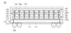
- FIG. 1a sectional view of a semiconductor device 100 according to an embodiment of the present invention is illustrated.
- the semiconductor device 100includes a substrate 110 , a first semiconductor die 120 formed on the substrate 110 , an interposer 130 formed on the substrate 110 , a second semiconductor die 140 formed on the interposer 130 , an encapsulant 170 formed to surround the first semiconductor die 120 , the interposer 130 and the second semiconductor die 140 , and solder balls 180 formed under the substrate 110 .
- the substrate 110provides a basis of the semiconductor device 100 according to an embodiment of the present invention.
- the substrate 110includes lands 112 formed on the lower surface of an insulating layer 111 , a plurality of conductive patterns 113 formed on the insulating layer 111 , conductive vias 114 penetrating the insulating layer 111 to connect the lands 112 to the conductive patterns 113 , and a solder mask 115 insulating the regions excluding the regions in which the lands 112 are formed.
- the insulating layer 111is plate-shaped.
- the insulating layer 111is made of an electrically insulating material such as thermosetting resin, polyimide, and polymer and primarily insulates electric elements on the insulating layer 111 from the outside.
- At least one or more lands 112are provided under the insulating layer 111 .
- the lands 112are electrically connected to an external circuit.
- the lands 112are electrically connected to the external circuit through the solder balls 180 .
- the lands 112are commonly made of copper having high conductivity or an equivalent thereof.
- the conductive patterns 113are formed on the insulating layer 111 .
- the conductive patterns 113are electrically connected to the first semiconductor die 120 , the interposer 130 , and/or the second semiconductor die 140 .
- the conductive patterns 113are commonly made of copper having high conductivity or an equivalent thereof.
- the conductive vias 114penetrate the insulating layer 111 and electrically connect the lands 112 to the conductive patterns 113 .
- the conductive vias 114may be formed by filling metal in via holes in forming the conductive patterns 113 .
- the solder mask 115is formed on the lower surface of the insulating layer 111 .
- the solder mask 115covers the regions excluding the regions in which the lands 112 are exposed to insulate the exclusive regions.
- the solder mask 115is made of benzocyclobutene (BCB) resin having high insulativity, polyimide, and an equivalent thereof.
- the first semiconductor die 120is formed on the substrate 110 using conductive bumps 120 a .
- the first semiconductor die 120has a through silicon via (TSV) structure. That is, the first semiconductor die 120 includes a plurality of bond pads 121 formed on one surface of the first semiconductor die 120 and through electrodes 122 that pass through the semiconductor die 120 .
- TSVthrough silicon via
- the bond pads 121are formed on the first semiconductor die 120 .
- the bond pads 121are illustrated to protrude above the first semiconductor die 120 .
- the bond pads 121may be actually formed inside the first semiconductor die 120 .
- the active surface of the first semiconductor die 120 , on which the bond pads 121 are formed,is illustrated to face upward, however, may be flipped if necessary.
- the through electrodes 122pass through the first semiconductor die 120 .
- the through electrodes 122are connected to correspond to the bond pads 121 . Therefore, an electric signal can be transmitted to the bond pads 121 from the lower surface of the first semiconductor die 120 .
- the through electrodes 122are connected to the conductive bumps 120 a to transmit the electric signal to the first semiconductor die 120 .
- the interposer 130is formed on the substrate 110 .
- the interposer 130is formed on the first semiconductor die 120 using conductive bumps 130 a to be electrically connected to the bond pads 121 .
- the interposer 130includes first regions 131 formed on the lower side thereof, second regions 132 formed thereon, conductive vias 133 for connecting the first regions 131 and the second regions 132 to each other, and integrated circuits 134 connected to the conductive vias 133 .
- the plurality of first regions 131are formed on the lower side of the interposer 130 .
- the first regions 131are connected to the bond pads 121 of the first semiconductor die 120 through the conductive bumps 130 a to input and output the electric signal.
- the first regions 131are made of copper having high conductivity or an equivalent thereof.
- the plurality of second regions 132are formed on the interposer 130 .
- the second regions 132are formed vertically on the first regions 131 to correspond to the first regions 131 .
- the second regions 132are also formed of copper having high conductivity or an equivalent thereof.
- the conductive vias 133are formed to pass through the interposer 130 to electrically connect the first regions 131 and the second regions 132 to each other.
- the conductive vias 133may be formed by filling metal in the via holes in forming the second regions 132 .
- the at least one or more integrated circuits 134are electrically connected to the conductive vias 133 .
- Each of the integrated circuits 134has a plurality of layers in the interposer 130 to perform individual functions.
- the integrated circuits 134may constitute a decoupling capacitor.
- the semiconductor device 100includes a second semiconductor die 140 provided on the first semiconductor die 120 .
- the integrated circuits 134 of the interposer 130 as decoupling capacitorsare provided between the first semiconductor die 120 and the second semiconductor die 140 to store the energy at the voltage applied from the substrate 110 .
- the energy stored in the integrated circuits 134is applied to the second semiconductor die 140 so that a constant voltage can be applied to the second semiconductor die 140 and that the reliability of operation can be improved.
- the integrated circuits 134may constitute an electrostatic discharge (ESD) protection circuit.
- ESDelectrostatic discharge
- the integrated circuits 134absorb the static electricity to prevent the electrostatic from being discharged.
- the integrated circuits 134may constitute an impedance matching circuit. There are various parasitic components in the first semiconductor die 120 or the second semiconductor die 140 in accordance with the structure of the first semiconductor die 120 or the second semiconductor die 140 and the transmission of a signal may be delayed. Therefore, the integrated circuits 134 perform phase compensation for the parasitic components through impedance matching.
- the plurality of integrated circuits 134perform one function selected from the functions, respectively.
- the integrated circuits 134are electrically connected to the second semiconductor die 140 through the second regions 132 connected through the conductive vias 133 .
- wiring linesare previously formed to the second semiconductor die 140 by fuses. Among the wiring lines, unnecessary wiring lines are removed by laser so that only some of the integrated circuits 134 may be connected to the second semiconductor die 140 .
- the second semiconductor die 140is formed on the interposer 130 and is electrically connected to the interposer 130 through conductive bumps 140 a .
- Bond pads 141are provided on one surface of the second semiconductor die 140 .
- the second semiconductor die 140is provided in the form of a flip-chip such that the bond pads 141 face downward.
- the second semiconductor die 141is connected to the second regions 132 of the interposer 130 to electrically transmit and receive a signal to and from the first semiconductor die 120 and the substrate 110 .
- FIG. 1illustrates the bond pads 141 of the second semiconductor die 140 to be flipped to face downward.
- the second semiconductor die 140may have a through silicon via (TSV) structure and may be formed such that the bond pads 141 face upward.
- TSVthrough silicon via
- the encapsulant 170is formed on the substrate 110 .
- the encapsulant 170encapsulates the first semiconductor die 120 , the interposer 130 , and the second semiconductor die 140 .
- the encapsulant 170protects the internal elements.
- the encapsulant 170may be made of one selected from the group consisting of common epoxy resin, silicon resin, and equivalents thereof.
- the solder balls 180are formed on the lower surface of the substrate 110 in the form of a ball to be electrically connected to the lands 112 .
- the solder balls 180are electrically connected to an external circuit so that an electric signal can be input to and output from the first semiconductor die 120 , the interposer 130 , and the second semiconductor die 140 .
- the solder balls 180may be made of a solder material.
- the integrated circuits 134 that perform the functions of the decoupling capacitor, the ESD preventing circuit, the impedance matching circuit, and the terminationare formed in the interposer 130 . Therefore, electric power can be smoothly supplied to the second semiconductor die 140 , the semiconductor device 100 can be protected from the ESD, and a signal can be smoothly transmitted so that the reliability of operation can be guaranteed.
- FIG. 2a sectional view of the semiconductor device 200 according to another embodiment of the present invention is illustrated.
- the semiconductor device 200includes a substrate 110 , a first semiconductor die 120 , an interposer 230 formed on the substrate 110 , a second semiconductor die 140 , an encapsulant 170 , and solder balls 180 .
- the interposer 230is formed on the first semiconductor die 120 using conductive bumps 230 a .
- the interposer 230is larger than the first semiconductor die 120 .
- the interposer 230includes first regions 231 formed on the lower surface of the interpose, second regions 232 formed thereon, conductive vias 233 connecting the first regions 231 and the second regions 232 to each other, and integrated circuits 234 connected to the conductive vias 233 .
- the interposer 230further includes passive elements 235 formed on the lower surface thereof.
- the passive elements 235are electrically connected to the first regions 231 through conductive bumps 236 .
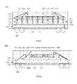
- FIG. 3a sectional view of a semiconductor device 300 according to still another embodiment of the present invention is illustrated.
- the semiconductor device 300includes a substrate 110 , a first die 120 , an interposer 330 formed on the first semiconductor die 120 , a second semiconductor die 340 formed on the first semiconductor die 120 , a third semiconductor die 350 formed on the second semiconductor die 340 , an encapsulant 170 , and solder balls 180 .
- the interposer 330is formed on one side of the first semiconductor die 120 .
- first regions 331 provided on the lower surface of the interposer 330are connected to the bond pads 121 of the first semiconductor die 120 through conductive bumps 330 a .
- Integrated circuits 334are electrically connected to conductive vias 333 for connecting the first regions 331 and second regions 332 to each other to function as the decoupling capacitor, the ESD preventing circuit, the impedance matching circuit, and the termination that are described above.
- the interposer 330divides the upper region of the first semiconductor die 120 from the second semiconductor die 340 . As a result, the interposer 330 supports the third semiconductor die 350 together with the second semiconductor die 340 . Therefore, when the third semiconductor die 350 larger than the second semiconductor die 340 is stacked, the third semiconductor die 350 is stably supported so that the physical force applied to the second semiconductor die 340 can be reduced.
- the second semiconductor die 340is formed on one side of the first semiconductor die 120 . Bond pads 341 are provided on the second semiconductor die 340 .
- the second semiconductor die 340is electrically connected to the first semiconductor die 120 through electrodes 342 connected to conductive bumps 340 a .
- the second semiconductor die 340is illustrated to be smaller than the first semiconductor die 120 and to run parallel with the interposer 330 . In addition, the second semiconductor die 340 may be flipped so that the surface on which the bond pads 341 are formed faces downward.
- the third semiconductor die 350is formed on the interposer 330 and the second semiconductor die 340 .
- the third semiconductor die 350is supported by the interposer 330 and the second semiconductor die 340 .
- the third semiconductor die 350is provided in the form of a flip chip so that bond pads 351 face downward and is connected to the second regions 332 of the interposer 330 through conductive bumps 350 a .
- the third semiconductor die 350has a TSV structure such that the bond pads 351 may face upward.
- FIG. 4a sectional view of the semiconductor device 400 according to still another embodiment of the present invention is illustrated.
- the semiconductor device 400includes a substrate 110 , a first die 420 formed on the substrate 110 , an interposer 430 formed on the first semiconductor die 420 , a second semiconductor die 440 formed on the interposer 430 , side interposers 460 formed on the sides of the second semiconductor die 440 , an encapsulant 170 , and solder balls 180 .
- the first semiconductor die 420is formed on the substrate 110 .
- the first semiconductor die 420includes bond pads 421 formed thereon, through electrodes 422 connected to the bond pads 421 passing through the semiconductor die 420 , and circumferential electrodes 423 positioned at the edges of the first semiconductor die 420 among the through electrodes 422 .
- the first semiconductor die 420may be flipped so that the bond pads 421 face downward.
- the circumferential electrodes 423 of the first semiconductor die 420are exposed to the sides of the first semiconductor die 420 . That is, the circumferential electrodes 423 are exposed through the sides of the first semiconductor die 420 as the edges of the first semiconductor die 420 are removed.
- the circumferential electrodes 422may be connected to the side interposers 460 .
- the interposer 430is formed on the first semiconductor die 420 .
- the interposer 430includes first regions 431 formed on the lower side thereof, second regions 432 formed thereon, conductive vias 433 for connecting the first regions 431 and the second regions 432 to each other, integrated circuits 434 , and circumferential vias 435 formed on the sides of the interposer 430 .
- the circumferential vias 435are formed at the edges of the interposer 430 among the conductive vias 433 and are exposed to the sides of the interposer 430 as the edges of the interposer 430 are removed.
- the circumferential vias 434may be connected to the side interposer 460 .
- the second semiconductor die 440is formed on the interposer 430 .
- the second semiconductor die 440is connected to the interposer 430 through conductive bumps 440 a by making bond pads 441 face downward.
- the second semiconductor die 440includes circumferential electrodes 442 having the TSV structure and formed at the edges.
- the circumferential electrodes 442penetrate the second semiconductor die 440 and are exposed to the sides of the second semiconductor die 440 .
- the circumferential electrodes 442may be connected to the side interposer 460 .
- the second semiconductor die 440may be positioned so that the bond pads 441 face upward.
- the side interposer 460is connected to at least one selected from the group consisting of the first semiconductor die 420 , the interposer 430 , and the second semiconductor die 440 .
- the side interposer 460includes first regions 461 formed on one surface, second regions 462 formed on the opposite surface thereof conductive vias 463 for connecting the first regions 461 and the second regions 462 to each other, and integrated circuits 464 connected to the conductive vias 463 .
- the first regions 461are connected to the first semiconductor die 420 , the interposer 430 , and/or the second semiconductor die 440 through conductive bumps 460 a .
- the integrated circuits 464may perform the same function as the integrated circuits 434 of the interposer 430 .
- the side interposers 460are positioned on the circumferences of the first semiconductor die 420 and the second semiconductor die 440 , it is possible to improve the space usability of the semiconductor device 400 according to still another embodiment of the present invention. Therefore, the side interposers 460 are provided so that it is possible to make the semiconductor device 400 according to still another embodiment of the present invention light, thin, short, and small.
- FIG. 5a sectional view of the semiconductor device 500 according to still another embodiment of the present invention is illustrated.
- the semiconductor device 500includes a substrate 110 , a first semiconductor die 120 , an interposer 130 , a second semiconductor die 540 formed on the interposer 130 , an encapsulant 170 , and solder balls 180 .
- the second semiconductor die 540is formed on the interposer 130 .
- the second semiconductor die 540is attached onto the interposer 130 by an adhesive 540 a .
- the adhesive 540 aelectrically insulates the lower surface of the second semiconductor die 540 from the second regions 132 of the interposer 130 .
- the second semiconductor die 540is electrically connected to the second regions 132 of the interposer 130 through conductive wires 540 b . Therefore, only parts having necessary functions among the integrated circuits 134 of the interposer 130 may be selectively connected to the second semiconductor die 540 .
- the second regions 132 of the interposer 130are independent of the integrated circuits 134 corresponding to the second regions 132 . If necessary, the second regions 132 may be selectively connected through the conductive wires 540 b . Therefore, since a fabrication method is simple, a large amount of interposers 130 can be produced.
- FIG. 6a sectional view of the semiconductor device 600 according to still another embodiment of the present invention is illustrated.
- the semiconductor device 600includes a substrate 110 , a first semiconductor die 620 formed on the substrate 110 , an interposer 630 formed on the first semiconductor die 620 , an encapsulant 170 , and solder balls 180 .
- the first semiconductor die 620is attached onto the substrate 110 by an adhesive 620 a .
- the first semiconductor die 620includes a plurality of bond pads 621 formed thereon.
- the bond pads 621are electrically connected to the conductive patterns 113 of the substrate 110 by conductive wires 620 b .
- the first semiconductor die 620 having the TSV structuremay be formed so that the bond pads 621 face the substrate 110 .
- the interposer 630is formed on the first semiconductor die 620 .
- the interposer 630is attached onto the first semiconductor die 620 by an adhesive 620 a.
- the interposer 630includes first regions 631 formed on the lower side thereof, second regions 632 formed thereon, conductive vias 633 for connecting the first regions 631 and the second regions 632 to each other, and integrated circuits 634 connected to the conductive vias 633 .
- the first regions 631are electrically independent of the first semiconductor die 620 by the adhesive 620 a .
- the second regions 632are electrically connected to the substrate 110 and/or the first semiconductor die 620 by the conductive wires 640 b.
- FIG. 7a sectional view of the semiconductor device 700 according to still another embodiment of the present invention is illustrated.
- the semiconductor device 700includes a substrate 110 , a first semiconductor die 620 , an interposer 730 formed on the first semiconductor die 620 , an encapsulant 170 , and solder balls 180 .
- the interposer 730is formed on the first semiconductor die 620 .
- the interposer 730is electrically connected to the bond pads 621 of the first semiconductor die 620 through conductive bumps 730 a . To this end, the interposer 730 is aligned with the bond pads 621 of the first semiconductor die 620 .
- the interposer 730includes first regions 731 formed on the lower surface thereof, second regions 732 formed thereon, conductive vias 733 for connecting the first regions 731 and the second regions 732 to each other, and integrated circuits 734 connected to the conductive vias 733 .
- FIG. 8is a flowchart illustrating a method of fabricating the semiconductor device 100 according to the embodiment of the present invention.
- FIGS. 9A to 9Eillustrate the method of fabricating the semiconductor device 100 according to the embodiment of the present invention.
- the semiconductor device 100includes forming a first semiconductor die (S 1 ), forming an interposer (S 2 ), forming a second semiconductor die (S 3 ), performing encapsulation (S 4 ), and forming solder balls (S 5 ).
- S 1first semiconductor die
- S 2interposer
- S 3second semiconductor die
- S 4performing encapsulation
- S 5solder balls
- the step (S 1 ) of forming the first semiconductor 120 on a substrate 110is performed.
- the first semiconductor die 120is formed to have the TSV structure.
- a plurality of bond pads 121are provided on the first semiconductor die 120 .
- the through electrodes 122 that pass through the first semiconductor die 120are connected to the bond pads 121 .
- the through electrodes 122 of the first semiconductor die 120are connected to the conductive patterns 113 of the substrate 110 through conductive bumps 120 a.
- the step (S 2 ) of forming the interposer 130 on the first semiconductor die 120is performed.
- the interposer 130is formed on the first semiconductor die 120 using the conductive bumps 130 a.
- the interposer 130includes first regions 131 formed on the lower surface thereof, second regions 132 formed thereon, conductive vias 133 for connecting the first regions 131 and the second regions 132 to each other, and at least one or more integrated circuits 134 connected to the conductive vias 133 .
- the integrated circuits 134may perform one function selected among the group consisting of a decoupling capacitor, an ESD preventing circuit, an impedance matching circuit, and termination.
- the step (S 3 ) of forming the second semiconductor die 140 on the interposer 130is performed.
- the second semiconductor die 140is formed on the interposer 130 using the conductive bumps 140 a.
- channelsmay be set to the region where the second semiconductor die 140 is attached by wiring lines through fuses. Then, when the remaining wiring lines excluding the wiring lines of the integrated circuits 134 having functions required for the second semiconductor die 140 and the second regions 132 connected thereto are removed by laser, only the integrated circuits 134 having the necessary functions can be connected to the second semiconductor die 140 .
- the second semiconductor die 140when the second semiconductor die 140 is connected onto the interposer 130 through conductive wires, it is not necessary for the second regions 132 of the interposer 130 to include additional wiring lines.
- the second regions 132 of the interposer 130 and the integrated circuits 134 connected theretomay be selectively connected to the second semiconductor die 140 by the conductive wires.
- the step (S 4 ) of performing encapsulation such that an encapsulant 170 surrounds the first semiconductor die 120 , the interposer 130 , and the second semiconductor die 140is performed.
- the encapsulant 170 used for encapsulationmay be formed of common epoxy resin and silicon resin and equivalents thereof. However, the content of the present invention is not limited to the above materials.
- the step (S 5 ) of forming solder balls 180 on the lower surface of the substrate 110is performed.
- the solder balls 180are electrically connected to the lands 112 of the substrate 110 .
- the solder balls 180may be made of at least one selected among the group consisting of tin, lead, silver, and a silver alloy or a combination of the above materials.
- the semiconductor device 100may be fabricated.
- the integrated circuits 134are provided in the interposer 130 to provide the functions of the decoupling capacitor, the ESD preventing circuit, the impedance matching circuit, and the termination and to improve reliability.
Landscapes
- Engineering & Computer Science (AREA)
- Microelectronics & Electronic Packaging (AREA)
- Power Engineering (AREA)
- Computer Hardware Design (AREA)
- Physics & Mathematics (AREA)
- Condensed Matter Physics & Semiconductors (AREA)
- General Physics & Mathematics (AREA)
- Semiconductor Integrated Circuits (AREA)
Abstract
Description
Claims (13)
Priority Applications (2)
| Application Number | Priority Date | Filing Date | Title |
|---|---|---|---|
| US12/535,316US8183678B2 (en) | 2009-08-04 | 2009-08-04 | Semiconductor device having an interposer |
| US13/454,972US8802494B2 (en) | 2009-08-04 | 2012-04-24 | Method of fabricating a semiconductor device having an interposer |
Applications Claiming Priority (1)
| Application Number | Priority Date | Filing Date | Title |
|---|---|---|---|
| US12/535,316US8183678B2 (en) | 2009-08-04 | 2009-08-04 | Semiconductor device having an interposer |
Related Child Applications (1)
| Application Number | Title | Priority Date | Filing Date |
|---|---|---|---|
| US13/454,972DivisionUS8802494B2 (en) | 2009-08-04 | 2012-04-24 | Method of fabricating a semiconductor device having an interposer |
Publications (2)
| Publication Number | Publication Date |
|---|---|
| US20110031598A1 US20110031598A1 (en) | 2011-02-10 |
| US8183678B2true US8183678B2 (en) | 2012-05-22 |
Family
ID=43534185
Family Applications (2)
| Application Number | Title | Priority Date | Filing Date |
|---|---|---|---|
| US12/535,316Active2030-07-20US8183678B2 (en) | 2009-08-04 | 2009-08-04 | Semiconductor device having an interposer |
| US13/454,972Active2029-11-10US8802494B2 (en) | 2009-08-04 | 2012-04-24 | Method of fabricating a semiconductor device having an interposer |
Family Applications After (1)
| Application Number | Title | Priority Date | Filing Date |
|---|---|---|---|
| US13/454,972Active2029-11-10US8802494B2 (en) | 2009-08-04 | 2012-04-24 | Method of fabricating a semiconductor device having an interposer |
Country Status (1)
| Country | Link |
|---|---|
| US (2) | US8183678B2 (en) |
Cited By (5)
| Publication number | Priority date | Publication date | Assignee | Title |
|---|---|---|---|---|
| US20110304010A1 (en)* | 2010-06-11 | 2011-12-15 | Industrial Technology Research Institute | Electrostatic discharge protection scheme for semiconductor device stacking process |
| US20120292757A1 (en)* | 2011-05-17 | 2012-11-22 | Infineon Technologies Ag | Semiconductor component and method of manufacturing a semiconductor component |
| US20140346668A1 (en)* | 2011-11-15 | 2014-11-27 | Rohm Co., Ltd. | Semiconductor device, method for manufacturing same, and electronic component |
| US9129935B1 (en) | 2012-10-05 | 2015-09-08 | Altera Corporation | Multi-chip packages with reduced power distribution network noise |
| US20150303172A1 (en)* | 2014-04-22 | 2015-10-22 | Broadcom Corporation | Reconstitution techniques for semiconductor packages |
Families Citing this family (65)
| Publication number | Priority date | Publication date | Assignee | Title |
|---|---|---|---|---|
| TWI420640B (en) | 2008-05-28 | 2013-12-21 | 矽品精密工業股份有限公司 | Semiconductor package device, semiconductor package structure, and method for fabricating the same |
| KR101563630B1 (en)* | 2009-09-17 | 2015-10-28 | 에스케이하이닉스 주식회사 | Semiconductor package |
| US8391018B2 (en)* | 2009-09-28 | 2013-03-05 | Qualcomm Incorporated | Semiconductor die-based packaging interconnect |
| US8053898B2 (en)* | 2009-10-05 | 2011-11-08 | Samsung Electronics Co., Ltd. | Connection for off-chip electrostatic discharge protection |
| US8618629B2 (en)* | 2009-10-08 | 2013-12-31 | Qualcomm Incorporated | Apparatus and method for through silicon via impedance matching |
| KR101046394B1 (en)* | 2010-02-03 | 2011-07-05 | 주식회사 하이닉스반도체 | Stack package |
| JP5826532B2 (en)* | 2010-07-15 | 2015-12-02 | 新光電気工業株式会社 | Semiconductor device and manufacturing method thereof |
| US8482111B2 (en) | 2010-07-19 | 2013-07-09 | Tessera, Inc. | Stackable molded microelectronic packages |
| US8598695B2 (en)* | 2010-07-23 | 2013-12-03 | Tessera, Inc. | Active chip on carrier or laminated chip having microelectronic element embedded therein |
| US8754516B2 (en)* | 2010-08-26 | 2014-06-17 | Intel Corporation | Bumpless build-up layer package with pre-stacked microelectronic devices |
| US8421245B2 (en)* | 2010-12-22 | 2013-04-16 | Intel Corporation | Substrate with embedded stacked through-silicon via die |
| US9064781B2 (en)* | 2011-03-03 | 2015-06-23 | Broadcom Corporation | Package 3D interconnection and method of making same |
| US8508045B2 (en) | 2011-03-03 | 2013-08-13 | Broadcom Corporation | Package 3D interconnection and method of making same |
| JP2012230961A (en)* | 2011-04-25 | 2012-11-22 | Elpida Memory Inc | Semiconductor device |
| KR101140113B1 (en)* | 2011-04-26 | 2012-04-30 | 앰코 테크놀로지 코리아 주식회사 | Semiconductor device |
| KR101128063B1 (en) | 2011-05-03 | 2012-04-23 | 테세라, 인코포레이티드 | Package-on-package assembly with wire bonds to encapsulation surface |
| US8836136B2 (en) | 2011-10-17 | 2014-09-16 | Invensas Corporation | Package-on-package assembly with wire bond vias |
| US8779849B2 (en)* | 2012-01-27 | 2014-07-15 | Micron Technology, Inc. | Apparatuses and methods for providing capacitance in a multi-chip module |
| US8946757B2 (en) | 2012-02-17 | 2015-02-03 | Invensas Corporation | Heat spreading substrate with embedded interconnects |
| US8835228B2 (en) | 2012-05-22 | 2014-09-16 | Invensas Corporation | Substrate-less stackable package with wire-bond interconnect |
| US20140001623A1 (en)* | 2012-06-28 | 2014-01-02 | Pramod Malatkar | Microelectronic structure having a microelectronic device disposed between an interposer and a substrate |
| US9502390B2 (en) | 2012-08-03 | 2016-11-22 | Invensas Corporation | BVA interposer |
| US9213386B2 (en) | 2012-10-22 | 2015-12-15 | Micron Technology, Inc. | Apparatuses and methods and for providing power responsive to a power loss |
| JP5543567B2 (en)* | 2012-10-22 | 2014-07-09 | 誠 雫石 | Manufacturing method of semiconductor device |
| US9799592B2 (en) | 2013-11-19 | 2017-10-24 | Amkor Technology, Inc. | Semicondutor device with through-silicon via-less deep wells |
| KR101366461B1 (en) | 2012-11-20 | 2014-02-26 | 앰코 테크놀로지 코리아 주식회사 | Semiconductor device and manufacturing method thereof |
| US9362252B2 (en) | 2013-03-13 | 2016-06-07 | Taiwan Semiconductor Manufacturing Company, Ltd. | Method and apparatus of ESD protection in stacked die semiconductor device |
| KR101473093B1 (en)* | 2013-03-22 | 2014-12-16 | 앰코 테크놀로지 코리아 주식회사 | Semiconductor device and manufacturing method thereof |
| US9167710B2 (en) | 2013-08-07 | 2015-10-20 | Invensas Corporation | Embedded packaging with preformed vias |
| US20150076714A1 (en) | 2013-09-16 | 2015-03-19 | Invensas Corporation | Microelectronic element with bond elements to encapsulation surface |
| US9583456B2 (en) | 2013-11-22 | 2017-02-28 | Invensas Corporation | Multiple bond via arrays of different wire heights on a same substrate |
| US9379074B2 (en) | 2013-11-22 | 2016-06-28 | Invensas Corporation | Die stacks with one or more bond via arrays of wire bond wires and with one or more arrays of bump interconnects |
| US9583411B2 (en) | 2014-01-17 | 2017-02-28 | Invensas Corporation | Fine pitch BVA using reconstituted wafer with area array accessible for testing |
| US10381326B2 (en)* | 2014-05-28 | 2019-08-13 | Invensas Corporation | Structure and method for integrated circuits packaging with increased density |
| US9412806B2 (en) | 2014-06-13 | 2016-08-09 | Invensas Corporation | Making multilayer 3D capacitors using arrays of upstanding rods or ridges |
| US9613857B2 (en)* | 2014-10-30 | 2017-04-04 | Taiwan Semiconductor Manufacturing Company, Ltd. | Electrostatic discharge protection structure and method |
| US9397038B1 (en) | 2015-02-27 | 2016-07-19 | Invensas Corporation | Microelectronic components with features wrapping around protrusions of conductive vias protruding from through-holes passing through substrates |
| US9888579B2 (en) | 2015-03-05 | 2018-02-06 | Invensas Corporation | Pressing of wire bond wire tips to provide bent-over tips |
| US9502372B1 (en) | 2015-04-30 | 2016-11-22 | Invensas Corporation | Wafer-level packaging using wire bond wires in place of a redistribution layer |
| US9761554B2 (en) | 2015-05-07 | 2017-09-12 | Invensas Corporation | Ball bonding metal wire bond wires to metal pads |
| US9490222B1 (en) | 2015-10-12 | 2016-11-08 | Invensas Corporation | Wire bond wires for interference shielding |
| US10490528B2 (en) | 2015-10-12 | 2019-11-26 | Invensas Corporation | Embedded wire bond wires |
| US10332854B2 (en) | 2015-10-23 | 2019-06-25 | Invensas Corporation | Anchoring structure of fine pitch bva |
| US10181457B2 (en) | 2015-10-26 | 2019-01-15 | Invensas Corporation | Microelectronic package for wafer-level chip scale packaging with fan-out |
| US10043779B2 (en) | 2015-11-17 | 2018-08-07 | Invensas Corporation | Packaged microelectronic device for a package-on-package device |
| JP6449760B2 (en)* | 2015-12-18 | 2019-01-09 | ルネサスエレクトロニクス株式会社 | Semiconductor device |
| US9984992B2 (en) | 2015-12-30 | 2018-05-29 | Invensas Corporation | Embedded wire bond wires for vertical integration with separate surface mount and wire bond mounting surfaces |
| US10734333B2 (en) | 2016-06-15 | 2020-08-04 | Intel Corporation | Semiconductor package having inductive lateral interconnects |
| US20180019194A1 (en)* | 2016-07-14 | 2018-01-18 | Semtech Corporation | Low Parasitic Surface Mount Circuit Over Wirebond IC |
| US9935075B2 (en) | 2016-07-29 | 2018-04-03 | Invensas Corporation | Wire bonding method and apparatus for electromagnetic interference shielding |
| US9960328B2 (en) | 2016-09-06 | 2018-05-01 | Amkor Technology, Inc. | Semiconductor device and manufacturing method thereof |
| KR102592640B1 (en)* | 2016-11-04 | 2023-10-23 | 삼성전자주식회사 | Semiconductor package and method of manufacturing the semiconductor package |
| US10299368B2 (en) | 2016-12-21 | 2019-05-21 | Invensas Corporation | Surface integrated waveguides and circuit structures therefor |
| US10374106B2 (en)* | 2017-04-13 | 2019-08-06 | Globalfoundaries Inc. | Integrated graphene detectors with waveguides |
| US10757800B1 (en) | 2017-06-22 | 2020-08-25 | Flex Ltd. | Stripline transmission lines with cross-hatched pattern return plane, where the striplines do not overlap any intersections in the cross-hatched pattern |
| KR102444290B1 (en)* | 2017-07-18 | 2022-09-16 | 삼성전자주식회사 | Interposer and integrated circuit chip bonding method, and ultrasonic probe using same |
| US10804115B2 (en) | 2017-08-03 | 2020-10-13 | General Electric Company | Electronics package with integrated interconnect structure and method of manufacturing thereof |
| US10541153B2 (en)* | 2017-08-03 | 2020-01-21 | General Electric Company | Electronics package with integrated interconnect structure and method of manufacturing thereof |
| US10541209B2 (en) | 2017-08-03 | 2020-01-21 | General Electric Company | Electronics package including integrated electromagnetic interference shield and method of manufacturing thereof |
| EP4170712A3 (en) | 2018-03-29 | 2023-07-12 | AT & S Austria Technologie & Systemtechnik Aktiengesellschaft | Electronic assembly and electronic system with impedance matched interconnect structures |
| US11224117B1 (en) | 2018-07-05 | 2022-01-11 | Flex Ltd. | Heat transfer in the printed circuit board of an SMPS by an integrated heat exchanger |
| US10964660B1 (en) | 2018-11-20 | 2021-03-30 | Flex Ltd. | Use of adhesive films for 3D pick and place assembly of electronic components |
| US10896877B1 (en)* | 2018-12-14 | 2021-01-19 | Flex Ltd. | System in package with double side mounted board |
| KR102762396B1 (en)* | 2019-02-14 | 2025-02-05 | 삼성전자주식회사 | An interposer and an electronic device including the same |
| US12244137B2 (en)* | 2022-05-13 | 2025-03-04 | Infineon Technologies Ag | ESD protection for multi-die integrated circuits (ICs) including integrated passive devices |
Citations (17)
| Publication number | Priority date | Publication date | Assignee | Title |
|---|---|---|---|---|
| US6104082A (en)* | 1998-04-24 | 2000-08-15 | International Business Machines Corporation | Metallization structure for altering connections |
| US6137161A (en)* | 1999-09-14 | 2000-10-24 | International Business Machines Corporation | Interposer array module for capacitive decoupling and filtering |
| US20020132533A1 (en)* | 2000-03-31 | 2002-09-19 | Figueroa David G, | Discrete device socket and method of fabrication therefor |
| US20040067605A1 (en)* | 2002-10-02 | 2004-04-08 | Shinko Electric Industries, Co., Ltd. | Semiconductor device having additional functional element and method of manufacturing thereof |
| US20040257749A1 (en)* | 2003-06-20 | 2004-12-23 | Ngk Spark Plug Co., Ltd. | Capacitor, capacitor equipped semiconductor device assembly, capacitor equipped circuit substrate assembly and electronic unit including semiconductor device, capacitor and circuit substrate |
| US20060012966A1 (en)* | 2000-07-31 | 2006-01-19 | Intel Corporation | Electronic assemblies and systems comprising interposer with embedded capacitors |
| US20060092595A1 (en)* | 2004-11-04 | 2006-05-04 | Samsung Electro-Mechanics Co., Ltd. | Multilayered chip capacitor array |
| US20060228855A1 (en)* | 2005-03-29 | 2006-10-12 | Intel Corporation | Capacitor with co-planar electrodes |
| US20070291448A1 (en)* | 2004-06-17 | 2007-12-20 | Apple Inc. | Interposer containing bypass capacitors for reducing voltage noise in an ic device |
| US20080054429A1 (en)* | 2006-08-25 | 2008-03-06 | Bolken Todd O | Spacers for separating components of semiconductor device assemblies, semiconductor device assemblies and systems including spacers and methods of making spacers |
| US7378733B1 (en)* | 2006-08-29 | 2008-05-27 | Xilinx, Inc. | Composite flip-chip package with encased components and method of fabricating same |
| US20080247116A1 (en)* | 2007-04-06 | 2008-10-09 | Ibiden Co., Ltd | Interposer, a method for manufacturing the same and an electronic circuit package |
| US20080296697A1 (en)* | 2007-05-29 | 2008-12-04 | Chao-Shun Hsu | Programmable semiconductor interposer for electronic package and method of forming |
| US20090079454A1 (en)* | 2006-08-04 | 2009-03-26 | John Ulrich Knickerbocker | Method of testing using a temporary chip attach carrier |
| US7863524B2 (en)* | 2006-09-26 | 2011-01-04 | Fujitsu Limited | Interposer and method for manufacturing the same |
| US20110096521A1 (en)* | 2007-02-12 | 2011-04-28 | Michael Randall | Electronic passive device |
| US7936060B2 (en)* | 2009-04-29 | 2011-05-03 | International Business Machines Corporation | Reworkable electronic device assembly and method |
Family Cites Families (2)
| Publication number | Priority date | Publication date | Assignee | Title |
|---|---|---|---|---|
| KR100486832B1 (en)* | 2002-02-06 | 2005-05-03 | 삼성전자주식회사 | Semiconductor Chip, Chip Stack Package And Manufacturing Method |
| KR100621991B1 (en)* | 2003-01-03 | 2006-09-13 | 삼성전자주식회사 | Chip Scale Stacking Package |
- 2009
- 2009-08-04USUS12/535,316patent/US8183678B2/enactiveActive
- 2012
- 2012-04-24USUS13/454,972patent/US8802494B2/enactiveActive
Patent Citations (18)
| Publication number | Priority date | Publication date | Assignee | Title |
|---|---|---|---|---|
| US6104082A (en)* | 1998-04-24 | 2000-08-15 | International Business Machines Corporation | Metallization structure for altering connections |
| US6137161A (en)* | 1999-09-14 | 2000-10-24 | International Business Machines Corporation | Interposer array module for capacitive decoupling and filtering |
| US20020132533A1 (en)* | 2000-03-31 | 2002-09-19 | Figueroa David G, | Discrete device socket and method of fabrication therefor |
| US20060012966A1 (en)* | 2000-07-31 | 2006-01-19 | Intel Corporation | Electronic assemblies and systems comprising interposer with embedded capacitors |
| US20040067605A1 (en)* | 2002-10-02 | 2004-04-08 | Shinko Electric Industries, Co., Ltd. | Semiconductor device having additional functional element and method of manufacturing thereof |
| US20040257749A1 (en)* | 2003-06-20 | 2004-12-23 | Ngk Spark Plug Co., Ltd. | Capacitor, capacitor equipped semiconductor device assembly, capacitor equipped circuit substrate assembly and electronic unit including semiconductor device, capacitor and circuit substrate |
| US20070291448A1 (en)* | 2004-06-17 | 2007-12-20 | Apple Inc. | Interposer containing bypass capacitors for reducing voltage noise in an ic device |
| US20060092595A1 (en)* | 2004-11-04 | 2006-05-04 | Samsung Electro-Mechanics Co., Ltd. | Multilayered chip capacitor array |
| US20060228855A1 (en)* | 2005-03-29 | 2006-10-12 | Intel Corporation | Capacitor with co-planar electrodes |
| US20090079454A1 (en)* | 2006-08-04 | 2009-03-26 | John Ulrich Knickerbocker | Method of testing using a temporary chip attach carrier |
| US20080054429A1 (en)* | 2006-08-25 | 2008-03-06 | Bolken Todd O | Spacers for separating components of semiconductor device assemblies, semiconductor device assemblies and systems including spacers and methods of making spacers |
| US7378733B1 (en)* | 2006-08-29 | 2008-05-27 | Xilinx, Inc. | Composite flip-chip package with encased components and method of fabricating same |
| US7696006B1 (en)* | 2006-08-29 | 2010-04-13 | Xilinx, Inc. | Composite flip-chip package with encased components and method of fabricating same |
| US7863524B2 (en)* | 2006-09-26 | 2011-01-04 | Fujitsu Limited | Interposer and method for manufacturing the same |
| US20110096521A1 (en)* | 2007-02-12 | 2011-04-28 | Michael Randall | Electronic passive device |
| US20080247116A1 (en)* | 2007-04-06 | 2008-10-09 | Ibiden Co., Ltd | Interposer, a method for manufacturing the same and an electronic circuit package |
| US20080296697A1 (en)* | 2007-05-29 | 2008-12-04 | Chao-Shun Hsu | Programmable semiconductor interposer for electronic package and method of forming |
| US7936060B2 (en)* | 2009-04-29 | 2011-05-03 | International Business Machines Corporation | Reworkable electronic device assembly and method |
Cited By (7)
| Publication number | Priority date | Publication date | Assignee | Title |
|---|---|---|---|---|
| US20110304010A1 (en)* | 2010-06-11 | 2011-12-15 | Industrial Technology Research Institute | Electrostatic discharge protection scheme for semiconductor device stacking process |
| US20120292757A1 (en)* | 2011-05-17 | 2012-11-22 | Infineon Technologies Ag | Semiconductor component and method of manufacturing a semiconductor component |
| US9177893B2 (en)* | 2011-05-17 | 2015-11-03 | Infineon Technologies Ag | Semiconductor component with a front side and a back side metallization layer and manufacturing method thereof |
| US20140346668A1 (en)* | 2011-11-15 | 2014-11-27 | Rohm Co., Ltd. | Semiconductor device, method for manufacturing same, and electronic component |
| US9478481B2 (en)* | 2011-11-15 | 2016-10-25 | Rohm Co., Ltd. | Semiconductor device, method for manufacturing same, and electronic component |
| US9129935B1 (en) | 2012-10-05 | 2015-09-08 | Altera Corporation | Multi-chip packages with reduced power distribution network noise |
| US20150303172A1 (en)* | 2014-04-22 | 2015-10-22 | Broadcom Corporation | Reconstitution techniques for semiconductor packages |
Also Published As
| Publication number | Publication date |
|---|---|
| US8802494B2 (en) | 2014-08-12 |
| US20130109135A1 (en) | 2013-05-02 |
| US20110031598A1 (en) | 2011-02-10 |
Similar Documents
| Publication | Publication Date | Title |
|---|---|---|
| US8183678B2 (en) | Semiconductor device having an interposer | |
| US6731009B1 (en) | Multi-die assembly | |
| KR101978020B1 (en) | Structure and formation method for chip package | |
| US12362263B2 (en) | Electronic package and method of fabricating the same | |
| US9449941B2 (en) | Connecting function chips to a package to form package-on-package | |
| KR100692441B1 (en) | Semiconductor device and manufacturing method of semiconductor device | |
| JP5514560B2 (en) | Semiconductor device | |
| US20140124907A1 (en) | Semiconductor packages | |
| US20140021591A1 (en) | Emi shielding semiconductor element and semiconductor stack structure | |
| KR101695846B1 (en) | Stacked semiconductor packages | |
| EP3051585A1 (en) | Chip package with embedded passive device | |
| US20080246135A1 (en) | Stacked package module | |
| US10950554B2 (en) | Semiconductor packages with electromagnetic interference shielding layer and methods of forming the same | |
| US12040304B2 (en) | Semiconductor package and method of fabricating the same | |
| KR20140057982A (en) | Semiconductor package and method of manufacturing the semiconductor package | |
| US20070096249A1 (en) | Three-dimensionally integrated electronic assembly | |
| US11728274B2 (en) | Semiconductor package and method of manufacturing the same | |
| US20080230886A1 (en) | Stacked package module | |
| KR101037827B1 (en) | Semiconductor package | |
| KR20140071561A (en) | Circuit board and semiconductor package including the same | |
| CN114121833A (en) | Electronic package, manufacturing method thereof and electronic structure | |
| KR20140082305A (en) | Stacked semiconductor package using of interposer | |
| US8603911B2 (en) | Semiconductor device and fabrication method thereof | |
| KR20160060380A (en) | Semiconductor package structure | |
| CN107403764B (en) | Electronic package |
Legal Events
| Date | Code | Title | Description |
|---|---|---|---|
| AS | Assignment | Owner name:AMKOR TECHNOLOGY KOREA, INC., KOREA, REPUBLIC OF Free format text:ASSIGNMENT OF ASSIGNORS INTEREST;ASSIGNORS:LEE, CHOON HEUNG;BAE, KI CHEOL;NA, DO HYUN;REEL/FRAME:023050/0318 Effective date:20090803 | |
| STCF | Information on status: patent grant | Free format text:PATENTED CASE | |
| AS | Assignment | Owner name:BANK OF AMERICA, N.A., TEXAS Free format text:PATENT SECURITY AGREEMENT;ASSIGNOR:AMKOR TECHNOLOGY, INC.;REEL/FRAME:029422/0178 Effective date:20120913 | |
| FPAY | Fee payment | Year of fee payment:4 | |
| AS | Assignment | Owner name:BANK OF AMERICA, N.A., AS AGENT, CALIFORNIA Free format text:SECURITY INTEREST;ASSIGNOR:AMKOR TECHNOLOGY, INC.;REEL/FRAME:046683/0139 Effective date:20180713 | |
| MAFP | Maintenance fee payment | Free format text:PAYMENT OF MAINTENANCE FEE, 8TH YEAR, LARGE ENTITY (ORIGINAL EVENT CODE: M1552); ENTITY STATUS OF PATENT OWNER: LARGE ENTITY Year of fee payment:8 | |
| AS | Assignment | Owner name:AMKOR TECHNOLOGY SINGAPORE HOLDING PTE.LTD., SINGAPORE Free format text:ASSIGNMENT OF ASSIGNORS INTEREST;ASSIGNOR:AMKOR TECHNOLOGY, INC.;REEL/FRAME:054067/0135 Effective date:20191119 | |
| MAFP | Maintenance fee payment | Free format text:PAYMENT OF MAINTENANCE FEE, 12TH YEAR, LARGE ENTITY (ORIGINAL EVENT CODE: M1553); ENTITY STATUS OF PATENT OWNER: LARGE ENTITY Year of fee payment:12 |