US8179639B2 - Head gimbal assembly without bus traces for plating - Google Patents
Head gimbal assembly without bus traces for platingDownload PDFInfo
- Publication number
- US8179639B2 US8179639B2US12/395,933US39593309AUS8179639B2US 8179639 B2US8179639 B2US 8179639B2US 39593309 AUS39593309 AUS 39593309AUS 8179639 B2US8179639 B2US 8179639B2
- Authority
- US
- United States
- Prior art keywords
- trace
- head gimbal
- gimbal assembly
- dielectric layer
- circuit
- Prior art date
- Legal status (The legal status is an assumption and is not a legal conclusion. Google has not performed a legal analysis and makes no representation as to the accuracy of the status listed.)
- Expired - Fee Related, expires
Links
Images


Classifications
- G—PHYSICS
- G11—INFORMATION STORAGE
- G11B—INFORMATION STORAGE BASED ON RELATIVE MOVEMENT BETWEEN RECORD CARRIER AND TRANSDUCER
- G11B5/00—Recording by magnetisation or demagnetisation of a record carrier; Reproducing by magnetic means; Record carriers therefor
- G11B5/48—Disposition or mounting of heads or head supports relative to record carriers ; arrangements of heads, e.g. for scanning the record carrier to increase the relative speed
- G11B5/4806—Disposition or mounting of heads or head supports relative to record carriers ; arrangements of heads, e.g. for scanning the record carrier to increase the relative speed specially adapted for disk drive assemblies, e.g. assembly prior to operation, hard or flexible disk drives
- G11B5/4853—Constructional details of the electrical connection between head and arm
Definitions
- a typical hard disc driveincludes one or more magnetic discs that are rotated by a spindle motor at a substantially constant high speed and accessed by an array of read/write heads that store data on tracks defined on the disc surfaces. Each head is carried by a slider which is designed to “fly” just over the surface of the rotating disc. Each slider is attached to a head gimbal assembly. Each head gimbal assembly includes a suspension and a head gimbal assembly circuit that carries electrical signals between the read/write head and hard disc drive electronics.
- Head gimbal assembliescan be manufactured in part by using an electroplating process. Electroplate processing requires that an electrical power or current source be connected to the head gimbal assemblies.
- the head gimbal assembliestypically will include bus traces to accomplish this electrical connection. Bus traces extend outside of the head gimbal assembly circuitry area to a point where they can be connected to a power source for electroplating. After electroplating, the bus traces are usually sheared, leaving a number of bus traces on the head gimbal assemblies with no further use. These bus traces and their associated processing have certain disadvantages such as causing distortion in electrical signals sent to and received from the read/write heads. Bus traces also require that an additional amount of area be added to HGA circuits. This may increase manufacturing costs and limit how close multiple head gimbal assemblies can be stacked together.
- Head gimbal assembliesfor data storage systems are provided.
- Head gimbal assembliesillustratively include a dielectric layer having a first and a second side. Some embodiments include a first conductive layer on the first dielectric layer. The first conductive layer illustratively includes a pad and a trace. Some embodiments include a second conductive layer on the second dielectric side. Some embodiments include a via that extends from the first dielectric layer side to the second dielectric layer side. The via illustratively electrically connects the first conductive layer to the second conductive layer.
- FIG. 1is a top view of a head gimbal assembly (HGA).
- HGAhead gimbal assembly
- FIG. 2is top view of a tail section of a HGA circuit.
- FIG. 3is a cross-section of a HGA circuit.
- FIG. 4is a bottom view of a tail section of a HGA circuit.
- FIG. 5-1is a cross-section of a HGA circuit.
- FIG. 5-2is a cross-section of another embodiment of a HGA circuit.
- FIG. 6is a bottom view of a head gimbal assembly.
- FIG. 7is a process flow for manufacturing a HGA circuit.
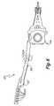
- FIG. 1is a top view of an embodiment of a head gimbal assembly (HGA) 200 .
- HGA 200may be incorporated into a disc drive.
- Each HGA 200includes a suspension 210 and a HGA circuit 250 .
- Each HGA circuitprovides an electrical pathway that facilitates communication between a slider read/write head and associated hard disc drive system electrical components including preamplifiers, controllers, flexures, printed circuit boards, or other components.
- Each suspensionmechanically supports a HGA circuit and a slider, and transfers motion from an actuator arm to a slider.
- suspension 210 and HGA circuit 250are two separate pieces. In another embodiment, suspension 210 and HGA circuit 250 are formed as one piece. Suspension 210 includes features such as aperture 215 that facilitate connecting HGA 200 to an actuator arm. Suspension 210 also includes features in its head gimbal region 220 that facilitate connecting a slider and an HGA circuit such as HGA circuit 250 to the suspension. HGA circuit 250 includes a tail section 255 , a body section 260 , and a head gimbal section 265 .
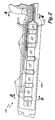
- FIG. 2is top view of tail section 255 of HGA circuit 250 .
- Tail section 255includes six pads 270 and six traces 275 .
- pads 270 and traces 275are made from an electrically conductive material such as copper, and are formed such that one pad and one trace are electrically connected to each other and are electrically isolated from the other pads and traces.
- Traces 275continue from tail section 255 and extend across HGA circuit body section 260 (shown in FIG. 1 ) until they reach HGA circuit head gimbal section 265 (also shown in FIG. 1 ). At head gimbal section 265 , traces 275 connect to and terminate at read/write head connection points.
- pads 270are electrically connected to a hard disc drive system electrical component such as a preamplifier, and read/write head connection points are electrically connected to a read/write head.
- tail section 255includes substrate openings 217 . Substrate openings 217 could be eliminated as design considerations warrant.
- HGA circuit 250facilitates communication from the slider read/write head to the hard disc drive components such that data can be read from and written to a recording medium.
- FIG. 3is an illustrative cross-section 300 of HGA circuit 250 at line 4 - 4 in FIG. 2 .
- Cross-section 300includes traces 275 .
- traces 275are made from an electrically conductive material such as copper. Traces 275 can be made from any conductive material.
- tracesare made from copper surrounded or encased by gold or by a gold/nickel alloy to reduce the possibility of exposed copper corroding.
- Cross-section 300also includes a coverlay layer 305 .
- coverlay 305covers or at least partially covers traces 275 .
- Embodiments of coverlay 305are made from a dielectric material such as polyimide that electrically isolates traces 275 .
- Coverlay 305also illustratively reduces the exposure of traces to harmful environmental conditions such as humidity and oxygen that could cause the traces to corrode.
- Cross-section 300also includes dielectric layer 310 .
- Dielectric layer 310is illustratively made from any electrically isolating material, in some embodiments polyimide.
- Dielectric layer 310provides physical support for traces 275 .
- Dielectric layer 310also electrically isolates traces 275 , pads 270 (shown in FIG. 2 ), and HGA circuit read/write head connections.
- cross-section 300includes substrate 315 .
- substrate 315provides physical support for the HGA circuit's electrically conductive and isolative layers, and provides features that are used in connecting the HGA circuit to a suspension such as suspension 210 (shown in FIG. 1 ).
- Substrate 315is made from any conductive material such as a metal (e.g. stainless steel). Substrate 315 can also be illustratively made from non-conductive materials.
- FIG. 4is a bottom view of tail section 255 of HGA circuit 250 .
- FIG. 4shows the same region of HGA circuit 250 as FIG. 2 including optional substrate openings 217 , but FIG. 4 shows the device lying on its opposite side (i.e. the side facing up in FIG. 2 is facing down in FIG. 4 ).
- FIG. 4includes substrate 315 and dielectric layer 310 (shown and previously discussed in describing FIG. 3 ).
- FIG. 4also includes islands 320 .
- Embodiments of HGA circuit 250also include vias as well as islands. As will be discussed later, islands and vias provide many advantages in device performance and manufacturing.
- islands 320are made from an electrically conductive material.
- islands 320 and substrate 315are made from the same material.
- each island 320is electrically isolated from one another and from substrate 315 .
- each island 320corresponds to one pad 270 (shown in FIG. 2 ).
- FIG. 5-1is an illustrative cross-section 400 of HGA circuit 250 at line 6 - 6 in FIG. 2 .
- Cross-section 400includes many of the features previously discussed such as coverlay 305 , pad 270 , traces 275 , dielectric layer 310 , substrate 315 , and island 320 .
- the configuration of trace 275 shown in FIG. 5-1is one embodiment. Other embodiments include different locations and sizes for trace 275 connecting to pad 270 .
- FIG. 5-1also includes via 405 .
- via 405is made from any electrically conductive material such as copper or stainless steel, and electrically connects island 320 and pad 270 .
- each island 320(shown in FIG.
- island 320is electrically connected throughout the HGA circuit 250 because it is electrically connected to pad 270 .
- island 320is electrically isolated from substrate 315 by isolation zone 317 .
- Isolation zone 317can be an area devoid of material in some embodiments. In other embodiments, isolation zone 317 can comprise an electrically insulating material like dielectric.
- FIG. 5-2is a cross-section of another embodiment of a HGA circuit.
- FIG. 5-2shows the same or similar features as FIG. 5-1 and is numbered accordingly.
- island 320 and via 405are not electrically connected to trace 275 through a pad such as pad 270 shown in FIG. 5-1 . Instead, island 320 and via 405 are directly connected to trace 275 .
- FIG. 6is a bottom view of an embodiment of a head gimbal assembly 200 .
- FIG. 6shows the same HGA 200 as FIG. 1 , but FIG. 6 shows the device lying on its opposite side (i.e. the side facing up in FIG. 1 is facing down in FIG. 6 ).
- FIG. 6includes HGA circuit islands 320 , HGA circuit substrate 315 , and suspension 210 .
- Islands 320 and vias 405may be positioned anywhere so long as they form an electrical connection to the pad and trace circuitry. Since the circuitry passes throughout the HGA circuit, this means that the islands and vias can be located almost anywhere on the HGA circuit. For example, FIG. 6 shows a large region 316 that is currently occupied by substrate 315 .
- this area or portions of this areainclude islands and vias 325 .
- Islands and vias 325are shown as circular in this alternate location embodiment. Embodiments of islands and vias are not however limited to any shape, size, or material.
- the HGA circuit head gimbal section 265(shown in FIG. 1 ) is largely obstructed by suspension 210 . In embodiments, that area, section 265 , includes islands and vias.
- HGA circuit manufacturingfrequently involves electroplating.
- padssuch as pads 270 and traces such as traces 275 are first formed out of copper or an alloy primarily consisting of copper. These largely copper pads and traces are then electroplated to form a gold, gold/nickel, or similar layer on top of the copper. These plated layers prevent copper corrosion and can improve electrical performance.
- One requirement of electroplating processesis that an electrical current needs to be ran through the metal being plated.
- Embodiments of HGA circuits with vias and islands such as HGA circuit 250do not need bus traces for electroplate processing. These HGA circuits provide higher performance by reducing the distortion in the high-speed electrical signals sent between the preamplifier and the read/write head caused by the bus traces. These HGA circuits also do not require the extra space on the device to include the bus traces. This enables these devices to be stacked more closely together to enable higher head and disc counts in disc drives.
- FIG. 7is an illustrative process flow 600 for manufacturing a HGA circuit with vias and islands such as HGA circuit 250 .
- Embodiments of HGA circuit 250are not limited to any particular process flow. Other embodiments of process flows for manufacturing HGA circuits with vias and islands also exist, and some illustrative examples of those will be described following the description of FIG. 7 . It should be noted that none of these process flows require bus traces for plating.
- Process 600begins at step 610 .
- a uniform piece of material that will be used as a substrateis obtained.
- An illustrative substrateis a flat and relatively thin piece of metal such as stainless steel. The material is uniform in that it has approximately the same thickness throughout its length and width.
- the length and width of the substrateneeds to be at least large enough to contain one HGA circuit.
- substratesare large enough that multiple HGA circuits are made from one substrate.
- An example of at least a portion of a substrate in a finished deviceis substrate 315 (shown in FIG. 3 ).
- a uniform layer of dielectric materialsuch as polyimide is deposited on the substrate.
- Process flow 600 and step 620are not limited to any one method of depositing the dielectric material. Illustrative methods include laminating a film of dielectric to the substrate, pouring a liquid mixture of dielectric material on the substrate surface and then drying it, and using chemical vapor deposition techniques.
- An example of at least a portion of a layer of dielectric material in a finished deviceis dielectric 310 (shown in FIG. 3 ).
- the dielectric material deposited at step 620is patterned so that the only material that will be left is the material that will form the dielectric layer in the finished devices such as dielectric layer 310 (shown in FIGS. 4 , 5 - 1 , and 5 - 2 ). It should be noted that this step includes patterning a hole where a via such as via 405 (shown in FIGS. 5-1 and 5 - 2 ) will be formed.
- process 600is not limited to any single patterning method
- one example of a patterning methodis to use a photolithographic process to form photoresist over the areas of the dielectric layer where dielectric is to remain, then to remove the exposed/unwanted dielectric with reactive ion etching, ion milling, or a wet etch, and then to remove the photoresist with a wet stripping process or an oxygen ashing process.
- An example of at least a portion of a patterned dielectric layer in a finished deviceis dielectric 310 (shown in FIGS. 5-1 and 5 - 2 to have been patterned for a hole for via 405 ).
- a seed layeris deposited on the substrate and the patterned dielectric layer.
- the seed layerfacilitates electroplating at step 660 by allowing material to be plated where the seed layer is deposited.
- photoresistis deposited on top of the seed layer. It is patterned such that photoresist blocks the areas that will not be covered by the plating material, and that the areas to be plated are free from photoresist.
- the areas that will be platedinclude the areas where the vias will be formed, where the traces will be formed, and where the pads will be formed.
- plating of the primary conductor layeris performed. It is worth noting that at this point in the process flow that the substrate material is still uniform (i.e. it has not been patterned).
- a power sourcei.e. source of electrical current
- a power sourceis connected to the substrate and one or more of another layer such as the dielectric layer, seed layer, or photoresist. After the power source is connected, the substrate and attached layers are put into a plating bath.
- copperis plated to form the vias, the pads, and the traces.
- Process 600is not limited to any specific type of plating machinery, process, or plating materials (e.g. copper, gold, nickel, etc.). Examples of at least a portion of plating in a finished device are via 405 , pad 270 (both shown in FIGS. 5-1 and 5 - 2 ), and traces 275 (shown in FIG. 3 ).
- Step 665the photoresist used to define the primary conductor layer is removed.
- Step 665is not limited to any particular methods, materials, or processes.
- Illustrative photoresist removal stepsinclude removing the photoresist with a wet stripping process, removing the photoresist with an oxygen ashing process, or removing the photoresist with a physical etch such as ion milling.
- the seed layer that was deposited at step 640is removed from the areas that were not plated with the primary conductor layer at step 660 (e.g. areas surrounding but not including the traces, pads, and vias).
- a protective coverlay layeris deposited on top of at least a portion of the plated traces.
- the coverlaymay also optionally be deposited on top of dielectric deposited at step 620 or the substrate at step 610 .
- the coverlayis of the same or similar type of material as the dielectric layer, and it is also deposited and patterned in a similar manner.
- the coverlayis patterned to only cover the desired portions of the devices.
- tracesare covered, but the pads and connections to the read/write head are not.
- Embodiments of HGA circuitsdo not have coverlay and thus do not include this processing step (i.e. this step is optional).
- An example of at least a portion of a coverlay layer in a finished deviceis coverlay 305 (shown in FIGS. 3 , 5 - 1 , and 5 - 2 ).
- plating of additional conductor layersis performed.
- Plating of additional conductor layersis optional.
- Additional conductor layers that may be platedinclude, but are not limited to, gold, nickel, or a combination of gold/nickel.
- the additional layersare illustratively used to prevent corrosion or improve device performance.
- Step 675is not limited to any particular methods, materials, or processes. Methods such as those described at step 660 are illustratively used.
- plating of additional conductor layersis not limited to any particular sequential order.
- the plating of additional conductor layerscan optionally be performed between steps 667 and steps 670 (i.e. plating the additional layers before depositing coverlay).
- the substrateis patterned.
- the same or similar methods used to pattern the dielectric layerare used to pattern the substrate (e.g. photolithography followed by wet etch).
- the substrateis patterned such that the only or substantially only areas of substrate remaining are the parts of the substrate that will be part of the finished HGA circuit.
- a substantial portion of substrate that will not be part of a HGA circuitmay be left to hold HGA circuits together for further processing.
- islandssuch as islands 320 (shown in FIG. 4 ) are patterned. As has been previously described, islands are electrically connected to vias and then to the pads, traces, and remaining HGA circuit circuitry.
- forming islandsare important to electrically isolate the signals traveling through the traces.
- further optional processesmay be done as needed or as desired. For example, if multiple HGA circuits are formed from one substrate, an optional mechanical separation process such as punching, stamping, or shearing may be needed to separate the devices into individual HGA circuits. Examples of at least a portion of patterned substrate in a finished device are island 320 and substrate 315 (both shown in FIGS. 5-1 and 5 - 2 ).
- the plating step 660occurred before the substrate patterning step 680 .
- the substrate patterning stepoccurs before the plating step.
- the substrateis first patterned. This patterning includes forming islands. Then, a conductive film is placed across the patterned substrate including the islands.
- the power or current sourceis electrically connected to the conductive film.
- the substrate, its attached layers, and the conductive filmare then placed in the plating bath or baths for plating. Following plating, the conductive film is removed. It is worth noting that in both this alternative process flow and flow 600 , that the plating step is performed without the use of bus traces as previously described.
- Embodimentsdescribe a HGA circuit manufacturing process commonly referred to as an additive process. That means that the circuit elements are formed by adding material to a simple substrate such as a flat piece of stainless steel.
- Embodimentsalso include a subtractive process.
- the starting substrateis more complex such as a stack of stainless steel, polyimide, and copper (with the polyimide between the stainless steel and copper).
- a subtractive processat least a couple parts of the finished circuit are formed by the starting substrate.
- a substratesuch as stainless steel, polyimide (or other dielectric), and copper is used.
- the stainless steel and dielectric layerare then patterned to form a via hole.
- a conductive materialis then filled or deposited in the hole to form a via and to electrically connect the via to the stainless steel.
- the copperis plated with, gold, gold/nickel, etc. by connecting the stainless steel to the electroplating power source.
- the copper and dielectric layerare patterned to form a via hole. Then after any desired process such as copper and dielectric patterning, a seed layer and photoresist are added on top of the copper side. The copper layer is then gold or nickel/gold plated by connecting the stainless steel to the electroplating power source.
- HGA circuit manufacturing process flows described aboveare only illustrative embodiments. Embodiments are not limited to any particular process flow. Numerous variations and methods are possible, and all are included in embodiments. Similarly, changes and new developments in HGA circuit manufacturing process flows are also included in embodiments.
- HGA circuit 250includes six traces and six pads. Embodiments include any number of traces and pads, including more or less than the illustrated six. Embodiments also include any additional circuitry known in the art or will be developed in the art that is added to HGA circuits.
Landscapes
- Adjustment Of The Magnetic Head Position Track Following On Tapes (AREA)
Abstract
Description
Claims (16)
Priority Applications (1)
| Application Number | Priority Date | Filing Date | Title |
|---|---|---|---|
| US12/395,933US8179639B2 (en) | 2009-03-02 | 2009-03-02 | Head gimbal assembly without bus traces for plating |
Applications Claiming Priority (1)
| Application Number | Priority Date | Filing Date | Title |
|---|---|---|---|
| US12/395,933US8179639B2 (en) | 2009-03-02 | 2009-03-02 | Head gimbal assembly without bus traces for plating |
Publications (2)
| Publication Number | Publication Date |
|---|---|
| US20100220414A1 US20100220414A1 (en) | 2010-09-02 |
| US8179639B2true US8179639B2 (en) | 2012-05-15 |
Family
ID=42666963
Family Applications (1)
| Application Number | Title | Priority Date | Filing Date |
|---|---|---|---|
| US12/395,933Expired - Fee RelatedUS8179639B2 (en) | 2009-03-02 | 2009-03-02 | Head gimbal assembly without bus traces for plating |
Country Status (1)
| Country | Link |
|---|---|
| US (1) | US8179639B2 (en) |
Cited By (2)
| Publication number | Priority date | Publication date | Assignee | Title |
|---|---|---|---|---|
| US9117469B1 (en)* | 2014-12-01 | 2015-08-25 | HGST Netherlands B.V. | Suspension design with split substrate for improved interference signal immunity |
| US20160104503A1 (en)* | 2010-05-24 | 2016-04-14 | Hutchinson Technology Incorporated | Low resistance ground joints for dual stage actuation disk drive suspensions |
Families Citing this family (27)
| Publication number | Priority date | Publication date | Assignee | Title |
|---|---|---|---|---|
| US8542465B2 (en) | 2010-03-17 | 2013-09-24 | Western Digital Technologies, Inc. | Suspension assembly having a microactuator electrically connected to a gold coating on a stainless steel surface |
| US8665567B2 (en) | 2010-06-30 | 2014-03-04 | Western Digital Technologies, Inc. | Suspension assembly having a microactuator grounded to a flexure |
| US9633680B2 (en) | 2010-10-29 | 2017-04-25 | Western Digital Technologies, Inc. | Head suspension having a flexure tail with a covered conductive layer and structural layer bond pads |
| US9165580B2 (en) | 2013-12-10 | 2015-10-20 | Western Digital Technologies, Inc. | Disk drive head suspension tail with stiffened edge alignment features |
| US8467153B1 (en) | 2010-10-29 | 2013-06-18 | Western Digital Technologies, Inc. | Disk drive head gimbal assembly having a flexure tail with folded bond pads |
| US9324344B1 (en) | 2013-12-10 | 2016-04-26 | Western Digital Technologies, Inc. | Disk drive head suspension tail with ground pad outside of bonding region |
| JP5075970B2 (en)* | 2010-11-30 | 2012-11-21 | 株式会社東芝 | Head gimbal assembly and disk device provided with the same |
| JP5713718B2 (en)* | 2011-02-17 | 2015-05-07 | 日本発條株式会社 | Flexure and head suspension provided with the same |
| JP6016047B2 (en)* | 2011-06-15 | 2016-10-26 | 大日本印刷株式会社 | Suspension board, suspension, suspension with head and hard disk drive |
| US8817423B2 (en)* | 2011-10-28 | 2014-08-26 | Nitto Denko Corporation | Circuit integrated suspension and method of manufacture thereof |
| WO2013138619A1 (en) | 2012-03-16 | 2013-09-19 | Hutchinson Technology Incorporated | Mid-loadbeam dual stage actuated (dsa) disk drive head suspension |
| CN104205216A (en) | 2012-03-22 | 2014-12-10 | 哈特奇桑科技公司 | Grounding Features for Disk Drive Head Suspension Flexures |
| JP6251745B2 (en) | 2012-09-14 | 2017-12-20 | ハッチンソン テクノロジー インコーポレイテッドHutchinson Technology Incorporated | Gimbal-type flexible member having two-stage starting structure and suspension |
| WO2014059128A2 (en) | 2012-10-10 | 2014-04-17 | Hutchinson Technology Incorporated | Co-located gimbal-based dual stage actuation disk drive suspensions with dampers |
| US8941951B2 (en) | 2012-11-28 | 2015-01-27 | Hutchinson Technology Incorporated | Head suspension flexure with integrated strain sensor and sputtered traces |
| US8891206B2 (en) | 2012-12-17 | 2014-11-18 | Hutchinson Technology Incorporated | Co-located gimbal-based dual stage actuation disk drive suspensions with motor stiffener |
| US8896969B1 (en) | 2013-05-23 | 2014-11-25 | Hutchinson Technology Incorporated | Two-motor co-located gimbal-based dual stage actuation disk drive suspensions with motor stiffeners |
| US8717712B1 (en) | 2013-07-15 | 2014-05-06 | Hutchinson Technology Incorporated | Disk drive suspension assembly having a partially flangeless load point dimple |
| US9330695B1 (en) | 2013-12-10 | 2016-05-03 | Western Digital Technologies, Inc. | Disk drive head suspension tail with a noble metal layer disposed on a plurality of structural backing islands |
| US8896970B1 (en) | 2013-12-31 | 2014-11-25 | Hutchinson Technology Incorporated | Balanced co-located gimbal-based dual stage actuation disk drive suspensions |
| US8867173B1 (en) | 2014-01-03 | 2014-10-21 | Hutchinson Technology Incorporated | Balanced multi-trace transmission in a hard disk drive flexure |
| US8934199B1 (en) | 2014-03-31 | 2015-01-13 | Western Digital Technologies, Inc. | Disk drive head suspension tail with bond pad edge alignment features |
| US9070392B1 (en) | 2014-12-16 | 2015-06-30 | Hutchinson Technology Incorporated | Piezoelectric disk drive suspension motors having plated stiffeners |
| US9318136B1 (en) | 2014-12-22 | 2016-04-19 | Hutchinson Technology Incorporated | Multilayer disk drive motors having out-of-plane bending |
| US9296188B1 (en) | 2015-02-17 | 2016-03-29 | Hutchinson Technology Incorporated | Partial curing of a microactuator mounting adhesive in a disk drive suspension |
| CN107735834B (en) | 2015-06-30 | 2019-11-19 | 哈钦森技术股份有限公司 | Disk drive head suspension structure with improved reliability |
| US9646638B1 (en) | 2016-05-12 | 2017-05-09 | Hutchinson Technology Incorporated | Co-located gimbal-based DSA disk drive suspension with traces routed around slider pad |
Citations (9)
| Publication number | Priority date | Publication date | Assignee | Title |
|---|---|---|---|---|
| US5401913A (en) | 1993-06-08 | 1995-03-28 | Minnesota Mining And Manufacturing Company | Electrical interconnections between adjacent circuit board layers of a multi-layer circuit board |
| US5883759A (en) | 1996-02-22 | 1999-03-16 | Seagate Technology, Inc. | Flex circuit head interconnect for improved electrical performance and ease of assembly |
| US6025988A (en) | 1998-12-17 | 2000-02-15 | Read-Rite Corporation | Interconnect adapter and head suspension assembly |
| US6534723B1 (en) | 1999-11-26 | 2003-03-18 | Ibiden Co., Ltd. | Multilayer printed-circuit board and semiconductor device |
| US7059868B1 (en) | 2000-03-07 | 2006-06-13 | Western Digital (Fremont), Inc. | Connection of trace circuitry in a computer disk drive system |
| US7203033B2 (en)* | 2002-10-02 | 2007-04-10 | Seagate Technology Llc | Head gimbal assembly with an integrated mechanical and electrical attachment and a stiff plate |
| US7372669B2 (en) | 2004-08-09 | 2008-05-13 | Hitachi Global Storage Technologies Netherlands B.V. | Magnetic disk drive, wiring connection structure and terminal structure |
| US7595963B1 (en)* | 2006-06-07 | 2009-09-29 | Western Digital Technologies, Inc. | Head gimbal assembly including a flexure with a first conductive trace disposed between a slider and a dielectric layer |
| US7924532B2 (en)* | 2006-12-05 | 2011-04-12 | Samsung Electronics Co., Ltd. | Head gimbal assembly of hard disk drive having support element in a bonding region of a slider |
- 2009
- 2009-03-02USUS12/395,933patent/US8179639B2/ennot_activeExpired - Fee Related
Patent Citations (9)
| Publication number | Priority date | Publication date | Assignee | Title |
|---|---|---|---|---|
| US5401913A (en) | 1993-06-08 | 1995-03-28 | Minnesota Mining And Manufacturing Company | Electrical interconnections between adjacent circuit board layers of a multi-layer circuit board |
| US5883759A (en) | 1996-02-22 | 1999-03-16 | Seagate Technology, Inc. | Flex circuit head interconnect for improved electrical performance and ease of assembly |
| US6025988A (en) | 1998-12-17 | 2000-02-15 | Read-Rite Corporation | Interconnect adapter and head suspension assembly |
| US6534723B1 (en) | 1999-11-26 | 2003-03-18 | Ibiden Co., Ltd. | Multilayer printed-circuit board and semiconductor device |
| US7059868B1 (en) | 2000-03-07 | 2006-06-13 | Western Digital (Fremont), Inc. | Connection of trace circuitry in a computer disk drive system |
| US7203033B2 (en)* | 2002-10-02 | 2007-04-10 | Seagate Technology Llc | Head gimbal assembly with an integrated mechanical and electrical attachment and a stiff plate |
| US7372669B2 (en) | 2004-08-09 | 2008-05-13 | Hitachi Global Storage Technologies Netherlands B.V. | Magnetic disk drive, wiring connection structure and terminal structure |
| US7595963B1 (en)* | 2006-06-07 | 2009-09-29 | Western Digital Technologies, Inc. | Head gimbal assembly including a flexure with a first conductive trace disposed between a slider and a dielectric layer |
| US7924532B2 (en)* | 2006-12-05 | 2011-04-12 | Samsung Electronics Co., Ltd. | Head gimbal assembly of hard disk drive having support element in a bonding region of a slider |
Cited By (3)
| Publication number | Priority date | Publication date | Assignee | Title |
|---|---|---|---|---|
| US20160104503A1 (en)* | 2010-05-24 | 2016-04-14 | Hutchinson Technology Incorporated | Low resistance ground joints for dual stage actuation disk drive suspensions |
| US9812160B2 (en)* | 2010-05-24 | 2017-11-07 | Hutchinson Technology Incorporated | Low resistance ground joints for dual stage actuation disk drive suspensions |
| US9117469B1 (en)* | 2014-12-01 | 2015-08-25 | HGST Netherlands B.V. | Suspension design with split substrate for improved interference signal immunity |
Also Published As
| Publication number | Publication date |
|---|---|
| US20100220414A1 (en) | 2010-09-02 |
Similar Documents
| Publication | Publication Date | Title |
|---|---|---|
| US8179639B2 (en) | Head gimbal assembly without bus traces for plating | |
| US7129418B2 (en) | Suspension board with circuit and producing method thereof | |
| JP2778627B2 (en) | Method for manufacturing combined transducer / sliding / suspension assembly | |
| EP0265721B1 (en) | A means of fabricating thin film magnetic read-write head/arm assemblies | |
| JP4909844B2 (en) | Integrated lead flexure with embedded traces | |
| CN103068152B (en) | Substrate for suspension | |
| CN101304635B (en) | Wiring circuit board | |
| JP5136311B2 (en) | Suspension board | |
| CN101727917A (en) | Suspension board with circuit | |
| US7851706B2 (en) | Flexible printed circuit and manufacturing method thereof | |
| US7489479B2 (en) | Electrical lead suspension having partitioned air slots | |
| JP5601563B2 (en) | Suspension substrate, suspension, suspension with head, hard disk drive, and method for manufacturing suspension substrate | |
| JP2011198402A (en) | Flexure substrate for suspension, suspension, suspension with head, and hard disk drive | |
| US5771569A (en) | Manufacturing method for magnetic head suspension | |
| KR100842780B1 (en) | Magnetic head and method of producing the same | |
| JP5601564B2 (en) | Suspension substrate, suspension, suspension with head, hard disk drive, and method for manufacturing suspension substrate | |
| JP2017117513A (en) | Suspension substrate, suspension, suspension with head, and hard disk drive | |
| JP2013206488A (en) | Substrate for suspension, suspension, element equipping suspension, hard disc drive, and manufacturing method of substrate for suspension | |
| US8320083B1 (en) | Electrical interconnect with improved corrosion resistance for a disk drive head suspension | |
| JP5640600B2 (en) | Flexure substrate for suspension, suspension, suspension with head, hard disk drive, and method for manufacturing suspension flexure substrate | |
| JP2016167334A (en) | Manufacturing method of suspension substrate | |
| JP6174843B2 (en) | Suspension substrate, suspension, suspension with element, hard disk drive, and manufacturing method of suspension substrate | |
| JP6145975B2 (en) | Suspension board, suspension, suspension with head, and hard disk drive | |
| JPH08235526A (en) | Magnetic head device and its production | |
| JP2000268314A (en) | Magnetic head and manufacturing method of magnetic head |
Legal Events
| Date | Code | Title | Description |
|---|---|---|---|
| AS | Assignment | Owner name:SEAGATE TECHNOLOGY LLC, CALIFORNIA Free format text:ASSIGNMENT OF ASSIGNORS INTEREST;ASSIGNORS:KLARQVIST, JON KARSTEN;RUSSELL, KEEFE MICHAEL;REEL/FRAME:022392/0476 Effective date:20090227 | |
| AS | Assignment | Owner name:WELLS FARGO BANK, NATIONAL ASSOCIATION, AS COLLATERAL AGENT AND SECOND PRIORITY REPRESENTATIVE, CALIFORNIA Free format text:SECURITY AGREEMENT;ASSIGNORS:MAXTOR CORPORATION;SEAGATE TECHNOLOGY LLC;SEAGATE TECHNOLOGY INTERNATIONAL;REEL/FRAME:022757/0017 Effective date:20090507 Owner name:JPMORGAN CHASE BANK, N.A., AS ADMINISTRATIVE AGENT AND FIRST PRIORITY REPRESENTATIVE, NEW YORK Free format text:SECURITY AGREEMENT;ASSIGNORS:MAXTOR CORPORATION;SEAGATE TECHNOLOGY LLC;SEAGATE TECHNOLOGY INTERNATIONAL;REEL/FRAME:022757/0017 Effective date:20090507 Owner name:JPMORGAN CHASE BANK, N.A., AS ADMINISTRATIVE AGENT Free format text:SECURITY AGREEMENT;ASSIGNORS:MAXTOR CORPORATION;SEAGATE TECHNOLOGY LLC;SEAGATE TECHNOLOGY INTERNATIONAL;REEL/FRAME:022757/0017 Effective date:20090507 Owner name:WELLS FARGO BANK, NATIONAL ASSOCIATION, AS COLLATE Free format text:SECURITY AGREEMENT;ASSIGNORS:MAXTOR CORPORATION;SEAGATE TECHNOLOGY LLC;SEAGATE TECHNOLOGY INTERNATIONAL;REEL/FRAME:022757/0017 Effective date:20090507 | |
| AS | Assignment | Owner name:SEAGATE TECHNOLOGY INTERNATIONAL, CALIFORNIA Free format text:RELEASE;ASSIGNOR:JPMORGAN CHASE BANK, N.A., AS ADMINISTRATIVE AGENT;REEL/FRAME:025662/0001 Effective date:20110114 Owner name:SEAGATE TECHNOLOGY LLC, CALIFORNIA Free format text:RELEASE;ASSIGNOR:JPMORGAN CHASE BANK, N.A., AS ADMINISTRATIVE AGENT;REEL/FRAME:025662/0001 Effective date:20110114 Owner name:SEAGATE TECHNOLOGY HDD HOLDINGS, CALIFORNIA Free format text:RELEASE;ASSIGNOR:JPMORGAN CHASE BANK, N.A., AS ADMINISTRATIVE AGENT;REEL/FRAME:025662/0001 Effective date:20110114 Owner name:MAXTOR CORPORATION, CALIFORNIA Free format text:RELEASE;ASSIGNOR:JPMORGAN CHASE BANK, N.A., AS ADMINISTRATIVE AGENT;REEL/FRAME:025662/0001 Effective date:20110114 | |
| AS | Assignment | Owner name:THE BANK OF NOVA SCOTIA, AS ADMINISTRATIVE AGENT, CANADA Free format text:SECURITY AGREEMENT;ASSIGNOR:SEAGATE TECHNOLOGY LLC;REEL/FRAME:026010/0350 Effective date:20110118 Owner name:THE BANK OF NOVA SCOTIA, AS ADMINISTRATIVE AGENT, Free format text:SECURITY AGREEMENT;ASSIGNOR:SEAGATE TECHNOLOGY LLC;REEL/FRAME:026010/0350 Effective date:20110118 | |
| ZAAA | Notice of allowance and fees due | Free format text:ORIGINAL CODE: NOA | |
| ZAAB | Notice of allowance mailed | Free format text:ORIGINAL CODE: MN/=. | |
| STCF | Information on status: patent grant | Free format text:PATENTED CASE | |
| AS | Assignment | Owner name:SEAGATE TECHNOLOGY INTERNATIONAL, CAYMAN ISLANDS Free format text:TERMINATION AND RELEASE OF SECURITY INTEREST IN PATENT RIGHTS;ASSIGNOR:WELLS FARGO BANK, NATIONAL ASSOCIATION, AS COLLATERAL AGENT AND SECOND PRIORITY REPRESENTATIVE;REEL/FRAME:030833/0001 Effective date:20130312 Owner name:SEAGATE TECHNOLOGY LLC, CALIFORNIA Free format text:TERMINATION AND RELEASE OF SECURITY INTEREST IN PATENT RIGHTS;ASSIGNOR:WELLS FARGO BANK, NATIONAL ASSOCIATION, AS COLLATERAL AGENT AND SECOND PRIORITY REPRESENTATIVE;REEL/FRAME:030833/0001 Effective date:20130312 Owner name:EVAULT INC. (F/K/A I365 INC.), CALIFORNIA Free format text:TERMINATION AND RELEASE OF SECURITY INTEREST IN PATENT RIGHTS;ASSIGNOR:WELLS FARGO BANK, NATIONAL ASSOCIATION, AS COLLATERAL AGENT AND SECOND PRIORITY REPRESENTATIVE;REEL/FRAME:030833/0001 Effective date:20130312 Owner name:SEAGATE TECHNOLOGY US HOLDINGS, INC., CALIFORNIA Free format text:TERMINATION AND RELEASE OF SECURITY INTEREST IN PATENT RIGHTS;ASSIGNOR:WELLS FARGO BANK, NATIONAL ASSOCIATION, AS COLLATERAL AGENT AND SECOND PRIORITY REPRESENTATIVE;REEL/FRAME:030833/0001 Effective date:20130312 | |
| FPAY | Fee payment | Year of fee payment:4 | |
| FEPP | Fee payment procedure | Free format text:7.5 YR SURCHARGE - LATE PMT W/IN 6 MO, LARGE ENTITY (ORIGINAL EVENT CODE: M1555); ENTITY STATUS OF PATENT OWNER: LARGE ENTITY | |
| MAFP | Maintenance fee payment | Free format text:PAYMENT OF MAINTENANCE FEE, 8TH YEAR, LARGE ENTITY (ORIGINAL EVENT CODE: M1552); ENTITY STATUS OF PATENT OWNER: LARGE ENTITY Year of fee payment:8 | |
| FEPP | Fee payment procedure | Free format text:MAINTENANCE FEE REMINDER MAILED (ORIGINAL EVENT CODE: REM.); ENTITY STATUS OF PATENT OWNER: LARGE ENTITY | |
| LAPS | Lapse for failure to pay maintenance fees | Free format text:PATENT EXPIRED FOR FAILURE TO PAY MAINTENANCE FEES (ORIGINAL EVENT CODE: EXP.); ENTITY STATUS OF PATENT OWNER: LARGE ENTITY | |
| STCH | Information on status: patent discontinuation | Free format text:PATENT EXPIRED DUE TO NONPAYMENT OF MAINTENANCE FEES UNDER 37 CFR 1.362 | |
| FP | Lapsed due to failure to pay maintenance fee | Effective date:20240515 | |
| AS | Assignment | Owner name:SEAGATE TECHNOLOGY PUBLIC LIMITED COMPANY, CALIFORNIA Free format text:RELEASE BY SECURED PARTY;ASSIGNOR:THE BANK OF NOVA SCOTIA;REEL/FRAME:072193/0001 Effective date:20250303 Owner name:SEAGATE TECHNOLOGY, CALIFORNIA Free format text:RELEASE BY SECURED PARTY;ASSIGNOR:THE BANK OF NOVA SCOTIA;REEL/FRAME:072193/0001 Effective date:20250303 Owner name:SEAGATE TECHNOLOGY HDD HOLDINGS, CALIFORNIA Free format text:RELEASE BY SECURED PARTY;ASSIGNOR:THE BANK OF NOVA SCOTIA;REEL/FRAME:072193/0001 Effective date:20250303 Owner name:I365 INC., CALIFORNIA Free format text:RELEASE BY SECURED PARTY;ASSIGNOR:THE BANK OF NOVA SCOTIA;REEL/FRAME:072193/0001 Effective date:20250303 Owner name:SEAGATE TECHNOLOGY LLC, CALIFORNIA Free format text:RELEASE BY SECURED PARTY;ASSIGNOR:THE BANK OF NOVA SCOTIA;REEL/FRAME:072193/0001 Effective date:20250303 Owner name:SEAGATE TECHNOLOGY INTERNATIONAL, CAYMAN ISLANDS Free format text:RELEASE BY SECURED PARTY;ASSIGNOR:THE BANK OF NOVA SCOTIA;REEL/FRAME:072193/0001 Effective date:20250303 Owner name:SEAGATE HDD CAYMAN, CAYMAN ISLANDS Free format text:RELEASE BY SECURED PARTY;ASSIGNOR:THE BANK OF NOVA SCOTIA;REEL/FRAME:072193/0001 Effective date:20250303 Owner name:SEAGATE TECHNOLOGY (US) HOLDINGS, INC., CALIFORNIA Free format text:RELEASE BY SECURED PARTY;ASSIGNOR:THE BANK OF NOVA SCOTIA;REEL/FRAME:072193/0001 Effective date:20250303 |