US8179051B2 - Serial configuration for dynamic power control in LED displays - Google Patents
Serial configuration for dynamic power control in LED displaysDownload PDFInfo
- Publication number
- US8179051B2 US8179051B2US12/367,672US36767209AUS8179051B2US 8179051 B2US8179051 B2US 8179051B2US 36767209 AUS36767209 AUS 36767209AUS 8179051 B2US8179051 B2US 8179051B2
- Authority
- US
- United States
- Prior art keywords
- led
- voltage
- indicator
- minimum
- led driver
- Prior art date
- Legal status (The legal status is an assumption and is not a legal conclusion. Google has not performed a legal analysis and makes no representation as to the accuracy of the status listed.)
- Expired - Fee Related, expires
Links
Images


Classifications
- H—ELECTRICITY
- H05—ELECTRIC TECHNIQUES NOT OTHERWISE PROVIDED FOR
- H05B—ELECTRIC HEATING; ELECTRIC LIGHT SOURCES NOT OTHERWISE PROVIDED FOR; CIRCUIT ARRANGEMENTS FOR ELECTRIC LIGHT SOURCES, IN GENERAL
- H05B45/00—Circuit arrangements for operating light-emitting diodes [LED]
- H05B45/40—Details of LED load circuits
- H05B45/44—Details of LED load circuits with an active control inside an LED matrix
- H05B45/46—Details of LED load circuits with an active control inside an LED matrix having LEDs disposed in parallel lines
- H—ELECTRICITY
- H05—ELECTRIC TECHNIQUES NOT OTHERWISE PROVIDED FOR
- H05B—ELECTRIC HEATING; ELECTRIC LIGHT SOURCES NOT OTHERWISE PROVIDED FOR; CIRCUIT ARRANGEMENTS FOR ELECTRIC LIGHT SOURCES, IN GENERAL
- H05B45/00—Circuit arrangements for operating light-emitting diodes [LED]
- H05B45/20—Controlling the colour of the light
- H—ELECTRICITY
- H05—ELECTRIC TECHNIQUES NOT OTHERWISE PROVIDED FOR
- H05B—ELECTRIC HEATING; ELECTRIC LIGHT SOURCES NOT OTHERWISE PROVIDED FOR; CIRCUIT ARRANGEMENTS FOR ELECTRIC LIGHT SOURCES, IN GENERAL
- H05B45/00—Circuit arrangements for operating light-emitting diodes [LED]
- H05B45/30—Driver circuits
- H05B45/37—Converter circuits
- H05B45/3725—Switched mode power supply [SMPS]
- H05B45/38—Switched mode power supply [SMPS] using boost topology
Definitions
- the present disclosurerelates generally to light emitting diodes (LEDs) and more particularly to LED drivers.
- LEDsLight emitting diodes
- LCDsliquid crystal displays
- the LEDsoften are arranged in parallel “strings” driven by a shared power source, each LED string having a plurality of LEDs connected in series. To provide consistent light output between the LED strings, each LED string typically is driven at a regulated current that is substantially equal among all of the LED strings.
- FIG. 1is a diagram illustrating a light emitting diode (LED) system having dynamic power management in accordance with at least one embodiment of the present disclosure.
- LEDlight emitting diode
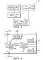
- FIG. 2is a flow diagram illustrating a method of operation of the LED system of FIG. 1 in accordance with at least one embodiment of the present disclosure.
- FIG. 3is a flow diagram illustrating a method for cascading an analog indicator of the minimum tail voltage of a plurality of LED strings for dynamic control in accordance with at least one embodiment of the present disclosure.
- FIG. 4is a flow diagram illustrating a method for cascading a digital indicator of the minimum tail voltage of a plurality of LED strings for dynamic control in accordance with at least one embodiment of the present disclosure.
- FIG. 5is a block diagram illustrating an example implementation of a cascaded LED driver of the LED system of FIG. 1 in accordance with at least one embodiment of the present disclosure.
- FIG. 6is a circuit diagram illustrating an analog implementation of a minimum detect module or a cascade controller of the cascaded LED driver of FIG. 5 in accordance with at least one embodiment of the present disclosure.
- FIG. 7is a diagram illustrating another analog implementation of a cascade controller of the cascaded LED driver of FIG. 5 in accordance with at least one embodiment of the present disclosure.
- FIG. 8is a diagram illustrating a digital implementation of the minimum detect module and the cascade controller of the cascaded LED driver of FIG. 5 in accordance with at least one embodiment of the present disclosure.
- FIG. 9is a diagram illustrating another digital implementation of the minimum detect module of the cascaded LED driver of FIG. 5 in accordance with at least one embodiment of the present disclosure.
- FIG. 10is a diagram illustrating an implementation of a feedback controller of the LED system of FIG. 1 based on a cascaded analog indicator of the minimum tail voltage of the plurality of LED strings of the LED system of FIG. 1 in accordance with at least one embodiment of the present disclosure.
- FIG. 11is a diagram illustrating an alternate implementation of the feedback controller of the LED system of FIG. 1 based on a cascaded indicator of the minimum tail voltage of the plurality of LED strings of the LED system of FIG. 1 in accordance with at least one embodiment of the present disclosure.
- FIG. 12is a diagram illustrating another example LED system implementing LED strings of different colors in accordance with at least one embodiment of the present disclosure.
- FIGS. 1-12illustrate example techniques for power management in a light emitting diode (LED) system having a plurality of LED strings.
- a power sourceprovides an output voltage to the head end of each of the plurality of LED strings to drive the LED strings.
- the LED systemincludes a plurality of LED drivers connected in series, each LED driver configured to regulate the current flowing through a corresponding subset of the plurality of LED strings.
- Each LED driverdetermines the minimum, or lowest, tail voltage of the LED strings of the corresponding subset, compares this with an indicator of a minimum tail voltage of one or more other subsets provided from an upstream LED driver in the series, and then provides an indicator of the lower voltage of the two tail voltages to the downstream LED driver in the series.
- an indicator of the overall minimum tail voltage of the plurality of LED stringsis cascaded through the series of LED drivers.
- a feedback controllermonitors the minimum tail voltage represented by the cascaded indicator and adjusts the output voltage of the power source accordingly.
- the feedback controlleradjusts the output voltage so as to maintain the overall minimum tail voltage of the plurality of LED strings at or near a predetermined threshold voltage. This ensures that the output voltage is sufficient to properly drive each active LED string at a regulated current with desired current accuracy and pulse width modulation (PWM) timing requirements without excessive power consumption.
- PWMpulse width modulation
- the series of LED driverscan be configured to cascade digital indicators of minimum tail voltages (e.g., as codes generated by analog-to-digital converters at the LED drivers) or to cascade analog indicators of minimum tail voltages (e.g., the minimum tail voltages themselves, or representations thereof).
- LED stringrefers to a grouping of one or more LEDs connected in series.
- the “head end” of a LED stringis the end or portion of the LED string which receives the driving voltage/current and the “tail end” of the LED string is the opposite end or portion of the LED string.
- tail voltagerefers the voltage at the tail end of a LED string or representation thereof (e.g., a voltage-divided representation, an amplified representation, etc.).
- subset of LED stringsrefers to one or more LED strings.
- FIG. 1illustrates a LED system 100 having dynamic power management in accordance with at least one embodiment of the present disclosure.
- the LED system 100includes a LED panel 102 , a plurality of LED drivers connected in series (e.g., LED drivers 104 , 105 , and 106 ), a feedback controller 108 , and a power source 110 .
- the LED panel 102includes a plurality of LED strings (e.g., LED strings 111 , 112 , 113 , 114 , 115 , and 116 ). Each LED string includes one or more LEDs 118 connected in series.
- the LEDs 118can include, for example, white LEDs, red, green, or blue (RGB) LEDs, organic LEDs (OLEDs), etc.
- the power source 110is configured to provide an output voltage V OUT having a magnitude adjusted based on an adjust signal 119 (ADJ). Each LED string is driven by the adjustable voltage V OUT received at the head end of the LED string via a voltage bus 120 (e.g., a conductive trace, wire, etc.).
- a voltage bus 120e.g., a conductive trace, wire, etc.
- the power source 110is implemented as a boost converter configured to drive the output voltage V OUT using an input voltage V IN .
- Each LED driverincludes a plurality of LED inputs and a corresponding plurality of current regulators.
- Each LED inputis configured to couple to a tail end of a corresponding LED string of a subset of the plurality of LED strings associated with the LED driver such that the current flow through the coupled LED string is regulated by the corresponding current regulator at or near a fixed current (e.g., 30 mA) when activated.
- a fixed currente.g. 30 mA
- the LED driver 104includes LED inputs 121 and 122 coupled to the tail ends of LED strings 111 and 112 , respectively, the LED driver 105 includes LED inputs 123 and 124 coupled to the tail ends of LED strings 113 and 114 , and the LED driver 106 includes LED inputs 125 and 126 coupled to the tail ends of LED strings 115 and 116 , respectively.
- the LED system 100is illustrated as having three LED drivers, with each LED driver being associated with a subset of two LED strings for ease of illustration, the techniques described herein are not limited to any particular number of LED drivers or any particular number of LED strings per LED driver.
- Each LED driveralso includes an input to receive pulse width modulation (PWM) data to control the activation, and timing thereof, of the LED strings of the corresponding subset via the current regulators of the LED driver.
- PWMpulse width modulation
- the LED driver 104includes an input 127 to receive PWM DATA A
- the LED driver 105includes an input 128 to receive PWM DATA B
- the LED driver 106includes an input 129 to receive PWM DATA C .
- Each LED drivercan receive the same PWM data or each LED driver can receive a different set of PWM data.
- each of the LED drivers 104 - 106may receive the same PWM data.
- each LED drivermay receive a different set of PWM data that is specific to the corresponding color type.
- each LED driverincludes an upstream interface and a downstream interface to facilitate connection of the LED drivers in series so as to serially communicate minimum tail voltage information between the LED drivers and to the feedback controller 108 .
- the LED driver 104includes an upstream interface 131 connected to an output interface 130 of the feedback controller 108 , and a downstream interface 132
- the LED driver 105includes an upstream interface 133 connected to the downstream interface 132 and a downstream interface 134
- the LED driver 106includes an upstream interface 135 connected to the downstream interface 134 and a downstream interface 136 connected to an input interface 138 of the feedback controller 108 .
- any of a variety of signaling architecturescan be used to facilitate communication between the downstream interface of one LED driver and the upstream interface of the next LED driver in the series (or between the output interface 130 and the upstream interface 131 or between the downstream interface 136 and the input interface 138 ).
- the serial connections between interfacescan include, for example, one wire interconnects (e.g., a 1-Wire® interconnect, an Inter-Integrated Circuit (I2C) interconnect, a System Management Bus (SMBus), or a proprietary interconnect architecture).
- the feedback controller 108includes the input interface 138 to receive an indicator of an overall minimum tail voltage of the plurality of LED strings 111 - 116 , the output interface 130 to provide a preset/trigger signal 140 to the first LED driver in the series (i.e., LED driver 104 ), and an output to provide the adjust signal 119 .
- the indicator of the overall minimum tail voltage of the plurality of LED strings 111 - 116can include a digital indicator (identified as code value C minFinal ), such as, for example, an ADC code value generated from the minimum tail voltage.
- the indicatorcan comprise an analog indicator (identified as voltage V TminFinal ), such as the minimum tail voltage itself, or a voltage derived from the minimum tail voltage.
- the feedback controller 108is configured to compare the overall minimum tail voltage represented by the received indicator to a threshold (voltage V thresh for an analog indicator or code value C thresh for a digital indicator) and adjust the adjust signal 119 based on the relationship between the overall minimum tail voltage and the threshold voltage so as to adjust the magnitude of the output voltage V OUT provided by the power source 110 based on this relationship.
- a thresholdvoltage V thresh for an analog indicator or code value C thresh for a digital indicator
- the LED system 100utilizes a feedback mechanism that permits the output voltage V OUT to be adjusted so as to reduce or minimize the power consumption of the LED drivers 104 , 105 and 106 in the presence of variances in voltage drop across the LED strings 111 - 116 , as described below with reference to the methods 200 , 300 , and 400 of FIG. 2 , 3 , and 4 , respectively.
- each of the LED drivers 104 - 106operates to activate the LED strings of their corresponding subsets based on activation and timing information determined from received PWM data.
- each of the LED driversoperates to determine the minimum tail voltage of the LED strings of its corresponding subset.
- the first LED driver in the seriesprovides, via the downstream interface, an indicator of the minimum tail voltage of the corresponding subset of LED strings to the upstream interface of the second LED string in the series.
- the second LED driver and each subsequent LED driver in the seriesdetermines the minimum tail voltage of the LED strings of its corresponding subset (referred to herein as the “local minimum tail voltage”), compares this local minimum tail voltage with the minimum tail voltage represented by the indicator received from the upstream LED driver, and then provides to the next LED driver an indicator that represents the lower of the local minimum tail voltage and the minimum tail voltage represented by the indicator received from the upstream LED driver.
- the last LED driver in the seriesprovides its indicator to the feedback controller 108 , which then uses the overall minimum tail voltage represented by the received indicator to adjust the output voltage V OUT as appropriate.
- the first LED driver in the cascaded seriesdoes not have an upstream LED driver (and thus an upstream minimum tail voltage with which to compare its local minimum tail voltage)
- the first LED driveris configured differently than the remainder of LED drivers in the cascaded series.
- the upstream interface of the first LED drivercan be fixedly pulled to a high voltage via one or more pull-up resistors so that when the first LED driver compares its local minimum tail voltage with the voltage at the upstream interface, the local minimum tail voltage is always the lower than the high voltage and thus always provided as the first indicator to the next LED driver in the series.
- the feedback controller 130can transmit a code having a particular predefined value (e.g., a code value of all “1's”) as the preset/trigger signal 140 so as to signal to the first LED driver that it is the first LED driver in the series.
- the first LED driverconfigures its operation so as to automatically provide the local minimum tail voltage as the first indicator without first requiring comparison with another indicator.
- the LED driver 104is the first LED driver in the series.
- the LED driver 104determines the local minimum tail voltage between the tail voltage V T1 of the LED string 111 and the tail voltage V T2 of the LED string 112 .
- the LED driver 104automatically provides an indicator 142 of the local minimum tail voltage of the LED strings 111 and 112 (identified as V TminA ) to the upstream interface 133 of the LED driver 105 .
- the provided indicator 142is an analog indicator, such as the voltage V TminA itself or a voltage derived therefrom.
- the LED driver 105digitizes the minimum tail voltage V TminA and provides a digital code value C minA as the indicator 142 .
- the LED driver 105determines the local minimum tail voltage between the tail voltage V T3 of the LED string 113 and the tail voltage V T4 of the LED string 114 , compares this local minimum tail voltage with the minimum tail voltage V TminA represented by the indicator 142 received from the LED driver 104 , and provides an indicator 144 of the lower of the two voltages.
- the indicator 144can be an analog indicator (identified as the voltage V TminB ) or a digital representation (identified as code C minB ).
- the LED driver 105then provides the indicator 144 to the upstream interface 135 of the LED driver 106 .
- the LED driver 106determines the local minimum tail voltage between the tail voltages V T5 and V T6 of the LED strings 115 and 116 , respectively, compares this local minimum tail voltage with the minimum tail voltage V TminB represented by the indicator 144 , and determines an indicator 146 as the lower of the two voltages (identified as voltage V TminC ).
- the indicator 146likewise can be an analog indicator or a digital indicator (identified as code C minC ).
- the indicator 146then is provided from the LED driver 106 to the feedback controller 108 as an indicator of the overall minimum tail voltage (V TminFinal or C minFinal ) of the plurality of LED strings 111 - 116 for use in controlling the output voltage V OUT as described herein.
- the indicator(either analog or digital) or other representation of the overall minimum tail voltage of the entire plurality of LED strings 111 - 116 is cascaded through the LED drivers 104 - 106 using a compare-and-forward approach such that the indicator output by the last LED driver in the series (e.g., LED driver 106 ) to the feedback controller 108 is an indicator of the lowest tail voltage of all of the LED strings 111 - 116 .
- This serial cascade between the LED drivers of the LED system 100 for minimum tail voltage feedback purposesrequires fewer and shorter interconnects between the LED drivers 105 - 107 and the feedback controller 108 than a star-type or spoke-and-hub-type configuration whereby each LED driver communicates the respective minimum tail voltage for its respective subset of LED strings directly back to the feedback controller.
- the feedback mechanism implemented by the cascaded LED drivers 104 - 106 and the feedback controller 108operates substantially continuously such that indicators of the minimum tail voltage of the plurality of LED strings 111 - 116 are continuously being cascaded through the LED drivers 104 - 106 and the feedback controller 108 is continuously adjusting the output voltage V OUT based on this continuous stream of indicators.
- frequent adjustment to the output voltage V OUTcan lead to overshooting or undershooting and other negative effects.
- the feedback mechanismoperates in a more periodic context whereby the minimum tail voltage of the plurality of LED strings 111 - 116 is determined once for any given feedback cycle and the corresponding indicator is then cascaded through the LED drivers 104 - 106 for use by the feedback controller 108 in periodically adjusting the output voltage V OUT .
- the feedback cycle of this mechanismcan include, for example, a PWM cycle or a portion thereof, multiple PWM cycles, a display frame cycle or a portion thereof, a certain number of clock cycles, a duration between interrupts, and the like.
- the components of the LED system 100can be implemented in separate integrated circuit (IC) packages.
- each of the LED drivers 104 - 106may be implemented as a separate IC package and the feedback controller 108 and some or all of the components of the power source 110 may be implemented together as another IC package 150 .
- the series arrangement of the LED drivers 104 - 106 and the feedback controller 108can facilitate extension of the LED system 100 to incorporate any number of LED strings subject only to timing restraints and power constraints because the feedback controller 108 requires only one output interface 130 and one input interface 138 to interface with a cascaded series of LED drivers regardless of the number of LED drivers in the series.
- a spoke-type arrangementwould require a feedback controller to have a separate interface to each LED driver, thereby causing the IC package implementing the feedback controller to be unnecessarily large to accommodate a large number of package pins for the interface requirements of the feedback controller.
- FIG. 2illustrates an example method 200 of operation of the power management mechanism of the LED system 100 of FIG. 1 in accordance with at least one embodiment of the present disclosure.
- the LED system 100is initiated by, for example, application of power or a power-on-reset (POR).
- the power source 110provides the output voltage V OUT to the head end of each of the plurality of LED strings 111 - 116 and the LED drivers 104 - 106 selectively activate LED strings of their respective subsets according to one or more sets of PWM data received at the LED drivers 104 - 106 .
- the LED drivers 104 - 106determine the local minimum tail voltage for the LED strings of their corresponding subsets and cascade the overall minimum tail voltage of the entire plurality of LED strings 111 - 116 through the LED drivers 104 - 106 to the feedback controller 108 .
- Example methods of operation of the LED drivers 104 - 106 for cascading the minimum tail voltage of the plurality of LED stringsare described below with reference to FIGS. 3 and 4 .
- the feedback controller 108receives an indicator of the overall minimum tail voltage of the plurality of LED strings 111 - 116 for a given point in time or for a given feedback cycle from the LED driver 106 .
- the feedback controller 108compares the minimum tail voltage represented by the analog indicator with a threshold V thresh to determine the relationship between the two voltages.
- the threshold voltage V threshis the expected minimum threshold of the tail voltage of a LED string needed to ensure proper current regulation of the LED string.
- the analog indicator of the overall minimum tail voltage of the plurality of LED strings 111 - 116is below the threshold voltage V thresh , there is a risk that one or more of the current regulators in the LED drivers 104 - 106 will be unable to effectively regulate the current in the corresponding LED string. Conversely, a situation whereby the analog indicator of the overall minimum tail voltage of the plurality of LED strings 111 - 116 is above the threshold voltage V thresh can lead to unnecessary power consumption by the LED strings.
- the feedback controller 108configures the adjust signal 119 so as to direct the power source 110 to increase the output voltage V OUT . Otherwise, in the event that the minimum tail voltage is greater than the threshold voltage V thresh , at block 212 the feedback controller 108 configures the adjust signal 119 so as to direct the power source 110 to decrease the output voltage V OUT . If the two voltages are equal, the feedback controller 108 can maintain the output voltage V OUT at its current level, or the output voltage V OUT can be adjusted up or down as appropriate.
- the feedback controller 108compares the digital indicator with the threshold code C thresh to determine the relationship between the two code values, whereby the code value C thresh can represent the expected minimum threshold of the tail voltage of a LED string needed to ensure proper current regulation of the LED string. Accordingly, in the event that the digital indicator of the overall minimum tail voltage of the plurality of LED strings 111 - 116 is less than the threshold code C thresh , at block 210 the feedback controller 108 configures the adjust signal 119 so as to direct the power source 110 to increase the output voltage V OUT .
- the feedback controller 108configures the adjust signal 119 so as to direct the power source 110 to decrease the output voltage V OUT . If the two codes are equal, the feedback controller 108 can maintain the output voltage V OUT at its current level, or the output voltage V OUT can be adjusted up or down as appropriate.
- indicators of the minimum tail voltage of the plurality of LED strings 111 - 116can be continuously cascaded through the feedback mechanism of the LED system 100 and thus the feedback process represented by blocks 206 , 208 , 210 , and 212 can be continuously repeated for each concurring point in time.
- a feedback cyclecan be used to synchronize the feedback mechanism to a timing reference, such as a PWM cycle, a clock cycle, or a display frame cycle, and thus the feedback process of blocks 206 , 208 , 210 , and 212 can be repeated for each feedback cycle.
- V TminA /C minA , V TminB /C minB , V TminC /C minC , and V TminFinal /C minFinalare the minimum indicators over the respective feedback cycle.
- FIG. 3illustrates an example method 300 of operation of a LED driver of the LED system 100 of FIG. 1 in cascading an analog indicator as part of the cascading process of block 206 of FIG. 2 in accordance with at least one embodiment of the present disclosure.
- the method 300represents the process repeated by each LED driver in the series with the exception of the first LED driver in the series (e.g., LED driver 104 , FIG. 1 ).
- the LED driverdetermines the local minimum tail voltage (V TminLocal ) from the tail voltages of the subset of the LED strings associated with the LED driver.
- the LED driveris configured to continuously provide the local minimum tail voltage.
- the LED driveris configured to periodically determine the local minimum tail voltage in response to a synchronization signal, such as a PWM cycle signal or a frame rate signal.
- the LED driverreceives, via the upstream interface, an analog indicator of the minimum tail voltage (V TminX ) of all of the LED strings associated with the LED drivers upstream of the present LED driver.
- the analog indicatoris the upstream minimum tail voltage itself, or a voltage representative of the upstream minimum tail voltage.
- the LED drivercompares the local minimum tail voltage V TminLocal with the upstream minimum tail voltage V TminX of all of the LED strings associated with the upstream LED drivers and provides to the downstream interface an analog indicator that represents the lower of these two voltages.
- the analog indicatoris thereby transmitted to the upstream interface of the next, or downstream, LED driver in the series.
- the first LED driver in the seriesoperates in a slightly different manner. Because there is no upstream LED driver for the first LED driver in the series, the first LED driver, in one embodiment, receives a signal (e.g., a particular data value) from the feedback controller 108 that signals to the first LED driver that it is to automatically provide the local minimum tail voltage as an indicator to the next LED driver in the series without performing the comparison described above.
- a signale.g., a particular data value
- the upstream interface of the first LED drivercan be pulled to a high voltage such that the local minimum tail voltage determined by the first LED driver is always lower than the voltage at the upstream interface of the first LED driver, thereby ensuring that the first LED driver provides its local minimum tail voltage as the indicator to the next LED driver in the series.
- FIG. 4illustrates an example method 400 of operation of a LED driver of the LED system 100 of FIG. 1 in cascading a digital indicator as part of the cascading process of block 206 of FIG. 2 in accordance with at least one embodiment of the present disclosure.
- the method 400represents the process repeated by each LED driver in the series with the exception of the first LED driver in the series (e.g., LED driver 104 , FIG. 1 ).
- the LED driverdetermines the local minimum tail voltage (V TminLocal ) from the tail voltages of the subset of the LED strings associated with the LED driver as similarly described at block 302 of FIG. 3 .
- the LED driverdigitizes the local minimum tail voltage V TminLocal using, for example an analog-to-digital converter (ADC) to generate a corresponding digital code C minLocal .
- ADCanalog-to-digital converter
- the LED driverreceives, via the upstream interface, a digital indicator (code C minX ) of the upstream minimum tail voltage (V TminX ) of all of the LED strings associated with the LED drivers upstream of the present LED driver.
- the digital indicatorcan include, for example, a digital code value generated by an ADC of an upstream LED driver from the minimum tail voltage V TminX as part of the application of the process represented by blocks 402 and 403 at an upstream LED driver.
- the LED driverdetermines the relationship between the code C minLocal and the code C minX and provides the lower of the two values to the downstream interface a digital indicator that is thereby transmitted to the next, or downstream, LED driver in the series.
- each LED driver in the seriesoperates to output to the next LED driver in the series an indicator (analog or digital) of the lowest minimum tail voltage of the LED strings determined by that point in the cascading series of LED drivers.
- FIG. 5illustrates an example implementation of a LED driver 500 (corresponding to the LED drivers 104 , 105 , and 106 of FIG. 1 ) in accordance with at least one embodiment of the present disclosure.
- the LED driver 500is described in the context of supporting a subset of two LED strings.
- the implementation of the LED driver 500is not limited to this number, or any particular number, of LED strings.
- the LED driver 500includes LED inputs 501 and 502 , an upstream interface 504 , a downstream interface 506 , a minimum detect module 508 , a cascade controller 510 , current regulators 511 and 512 , and a data/timing controller 514 .
- the LED input 501is configured to couple to a tail end of a first LED string (having a variable tail voltage V TX ) of the subset and the LED input 502 is configured to couple to a tail end of a second LED string (having a variable tail voltage V TY ) of the subset.
- the current regulator 511is configured to activate the first LED string and regulate the current through the first LED string based on control signaling from the data/timing controller 514 .
- the current regulator 512is configured to activate the second LED string and regulate the current through the second LED string based on control signaling from the data/timing controller 514 .
- the upstream interface 504is configured to couple to the downstream interface of an upstream LED driver and the downstream interface 506 is configured to couple to the upstream interface of a downstream LED driver.
- the minimum detect module 508includes inputs coupled to the LED inputs 501 and 502 to receive the tail voltages V TX and V TY and an output to provide an indicator of the lower of these two tail voltages as the indicator of the local minimum tail voltage for the subset of LED strings managed by the LED driver 500 .
- the minimum detect module 508continuously provides the indicator of the local minimum tail voltage.
- the indicator output of the minimum detect module 508can include, for example, the voltage V TminLocal that the minimum detect module 508 continuously varies as the voltages V TX and V TY vary.
- the indicator output of the minimum detect module 508can include a stream of code values generated by an ADC from the lower of the voltages V TX and V TY at any given point of a clock reference used by the ADC.
- the minimum detect module 508is synchronized to a given feedback cycle using a sync signal 516 such that the minimum detect module 508 outputs a single indicator (digital or analog) for every given feedback cycle.
- the sync signal 516can be generated by the data/timing controller 514 from the PWM data or the sync signal 516 can be received (as upstream sync signal from the upstream LED driver via the upstream interface 504 . Further, the sync signal 516 can be propagated to, or regenerated for, the downstream LED driver via the downstream interface 506 .
- Example implementations of the minimum detect module 508are illustrated below with reference to FIGS. 6 , 8 , and 9 .
- the cascade controller 510includes an input to receive, via the upstream interface 504 , an indicator (V TminA /C minA ) representative of the cumulative minimum tail voltage determined from the upstream LED drivers, an input to receive the local minimum tail voltage indicator(s) from the minimum detect module 508 , and an output to provide an indicator (V TminB /C minB ) representative of the cumulative minimum tail voltage determined from the upstream LED drivers and the LED driver 500 .
- the cascade controller 510compares the cumulative minimum tail voltage represented by the indicator received from the upstream LED driver with the local minimum tail voltage represented by the indicator received from the minimum detect module 508 and provides the indicator representative of the lower of the two as the downstream indicator (V TminB /C minB ).
- the cascade controller 510is configured to continuously perform this comparison process. In another embodiment, the cascade controller 510 is synchronized to a given feedback cycle using the sync signal 516 such that the cascade controller 510 outputs a single indicator (digital or analog) for every given feedback cycle. Example implementations of the cascade controller 510 are illustrated below with reference to FIGS. 7 and 8 .
- the data/timing control controller 514receives PWM data associated with the LED strings of the corresponding subset and is configured to provide control signals to the other components of the LED driver 500 based on the timing and activation information represented by the PWM data. To illustrate, the data/timing controller 514 provides control signals to the current regulators 511 and 512 to control which of the LED strings are active during corresponding portions of their respective PWM cycles. The data/timing control module 514 also can provide the sync signal 516 to control the timing of the minimum detect module 508 and the cascade controller 510 .
- FIG. 6illustrates an analog implementation of the minimum detect module 508 of FIG. 5 as a diode-OR circuit in accordance with at least one embodiment of the present disclosure.
- the diode-OR circuitcan include forward-biased diodes (e.g., LED diodes 601 and 602 for the two LED strings managed by the LED driver 500 ), each diode having an anode coupled to the tail end of a corresponding LED string of the subset and a cathode connected to an output node 603 that serves to provide the minimum tail voltage V TminLocal of the subset of LED strings connected to the diode-OR circuit (less the forward voltage drop of the diodes).
- the minimum detect module 508can include a compensation circuit 604 to cancel or compensate for the forward voltage drop of the diodes.
- FIG. 6also can be adapted for implementation of a diode-OR circuit for the cascade controller 510 ( FIG. 5 ) so as to select between the indicator of the local minimum tail voltage or an incoming indicator from an upstream LED driver.
- FIG. 7illustrates another analog implementation of the cascade controller 510 of FIG. 5 in accordance with at least one embodiment of the present disclosure.
- the cascade controller 510includes an analog multiplexer 702 (or switch) having one voltage input to receive the local minimum tail voltage V TminLocal generated by the minimum detect module 508 ( FIG. 5 ), another voltage input to receive the cumulative minimum tail voltage (V TminA ) represented by the indicator received from the upstream LED driver, and an output to provide a select one of the two input voltages as the cumulative minimum tail voltage (V TminB ) for the LED driver downstream of the LED driver 500 based on the state of a select signal 704 .
- V TminLocalgenerated by the minimum detect module 508 ( FIG. 5 )
- V TminAcumulative minimum tail voltage
- V TminBcumulative minimum tail voltage
- the analog multiplexer 702can include an enable input to receive the sync signal 516 ( FIG. 5 ) so that the analog multiplexer 702 synchronizes its output to the feedback cycle represented by the sync signal 516 .
- the cascade controller 510further includes an analog comparator 706 comprising an input to receive the local minimum tail voltage V TminLocal generated by the minimum detect module 508 , an input to receive the cumulative minimum tail voltage (V TminA ) represented by the indicator received from the upstream LED driver, and an output to configure the state of the select signal 704 based on the relationship between the voltage V TminLocal and the voltage V TminA so as to direct the analog multiplexer 702 to output the lower of the two voltages.
- FIG. 8illustrates an example implementation of the minimum detect module 508 and the cascade controller 510 in the context of digital indicators in accordance with at least one embodiment of the present disclosure.
- the minimum detect module 508includes a mechanism to determine the local minimum tail voltage V TminLocal of the subset of LED strings associated with the LED driver 500 ( FIG. 5 ), such as by using the diode-OR circuit of FIG. 6 .
- the minimum detect module 508further includes an ADC 802 to generate a code value C minLocal representative of the level of the local minimum tail voltage V TminLocal at a particular point in time or during a feedback cycle (e.g., as signaled by the sync signal 516 ).
- the ADC 802 or another minimum select modulecan be configured to select the lowest code value generated for the feedback cycle as the code value C minLocal .
- the cascade controller 510includes a digital multiplexer 804 , a digital comparator 806 , and buffers 808 , 810 , and 812 .
- the buffer 808stores the code C minA received from the upstream LED driver (and which represents the cumulative minimum tail voltage of the LED strings of the upstream LED drivers), the buffer 810 stores the code value C minLocal generated by the ADC 802 , and the buffer 812 stores a code C minB that is provided to the LED driver downstream of the LED driver 500 .
- the multiplexer 804includes an input coupled to the buffer 808 , an input coupled to the buffer 810 , an input to receive a select signal 814 , and an output coupled to the buffer 812 , whereby the digital multiplexer 804 selects either the value stored in the buffer 808 or the value stored in the buffer 810 for output to the buffer 812 based on the state of the select signal 814 .
- the digital comparator 806includes an input coupled to the buffer 808 , an input coupled to the buffer 810 and an output to provide the select signal 814 .
- the digital comparator 806compares the code C minA in the buffer 808 with the code C minLocal in the buffer 810 and directs the multiplexer 804 to output the lower of the two codes via the select signal 814 . Further, either or both the multiplexer 804 and the digital comparator 806 can be synchronized to a feedback cycle via the sync signal 516 .
- FIG. 9illustrates another example implementation of the minimum detect module 508 ( FIG. 5 ) in a digital indicator context in accordance with at least one embodiment of the present disclosure.
- the minimum detect module 508includes ADCs 902 and 904 and a code selector 906 .
- the ADC 902has an input coupled to the tail end of a first LED string and an output to provide one or more codes C 1 representative of the level of the tail voltage V TX of the first LED string at corresponding points in time.
- the ADC 904has an input coupled to the tail end of a second LED string and an output to provide one or more codes C 2 representative of the level of the tail voltage V TY of the second LED string at corresponding points in time.
- the code selector 906receives the codes output by the ADCs 902 and 904 and selects the lowest code of the received codes for output as the code C minLocal described above. In one embodiment, the code selector 906 compares codes as they are received and thus produces a stream of codes C minLocal at the rate of the code generation by the ADCs 902 and 904 . In another embodiment, the ADCs 902 and 904 each generate a respective stream of codes over a given feedback cycle and the code selector 906 continuously monitors the generated codes to identify the lowest code generated during the feedback cycle.
- the code selector 906outputs the lowest code for the feedback cycle as the code C minLocal for that feedback cycle.
- the code C minLocalthen can be forwarded to the downstream LED driver as part of the cascading process described above.
- FIG. 10illustrates an example implementation of the feedback controller 108 of the LED system 100 of FIG. 1 in an analog indicator context in accordance with at least one embodiment of the present disclosure.
- the feedback controller 108includes a voltage reference 1002 to generate the threshold voltage V thresh and a error amplifier 1004 having an input to receive the final analog indicator (V TminFinal ) from the last LED driver in the series, an input to receive the threshold voltage V thresh , and an output to provide the adjust signal 119 based on the relationship of the two input voltages.
- the error amplifier 1004configures the adjust signal 119 so as to direct the power source 110 ( FIG.
- FIG. 11illustrates another example implementation of the feedback controller 108 of the LED system 100 of FIG. 1 in a digital indicator context in accordance with at least one embodiment of the present disclosure.
- the feedback controller 108includes a code processing module 1102 , a digital-to-analog converter (DAC) 1104 , an error amplifier 1106 , and a voltage divider 1108 .
- DACdigital-to-analog converter
- the voltage divider 1108includes resistors 1111 and 1112 connected in series.
- the resistor 1111has a terminal coupled to the output of the power source 110 ( FIG. 1 ) to receive the output voltage and a terminal coupled to a node 1113 that provides a voltage V fb , whereby the resistor 1111 has a resistance R f1 .
- the resistor 1112has a terminal coupled to the node 1113 , a terminal connected to a ground reference, and a resistance R f2 .
- the code processing module 1102receives the cascaded code C minFinal from the last LED driver in the series and generates a code value C reg based on the relationship of the minimum tail voltage V TminFinal to the threshold voltage V thresh revealed by the comparison of the code value C minFinal to a code value C thresh that represents the voltage V thresh .
- the value of the code value C regaffects the resulting change in the output voltage V OUT .
- the code processing module 1102compares the code value C minFinal to the code value C thresh . If the code value C minFinal is less than the code value C thresh , an updated value for C reg is generated so as to increase the output voltage V OUT .
- the code value C minFinalis greater than the code value C thresh
- an updated value for C regis generated so as to decrease the output voltage V OUT .
- the resulting code C regis provided to the DAC 1104 , which converts the code C reg to a corresponding voltage V reg .
- the error amplifier 1106configures the adjust signal 119 based on the relationship of the voltage V reg to the voltage V fb so as to adjust the output voltage V OUT as described above.
- the control of the output voltage V OUTis based on the relationship between the feedback voltage V fb and the voltage V reg and thus dependent on the resistances R f1 and R f2 of the voltage divider 1108 , the gain of the DAC 1104 , and the gain of the ADC of the LED driver that generated the code C minFinal .
- the updated value for C regcan be set to
- the offset 1 valuecan be either positive or negative.
- FIG. 12illustrates an example LED system 1200 utilizing LED strings of different colors in accordance with at least one embodiment of the present disclosure.
- different color LEDsare used to provide the color components of the displayed image.
- certain LED systemsemploy separate red, green, and blue LED strings to achieve the RGB color scheme.
- LEDs of different colorsoften have different operating characteristics and thus often are operated at different fixed currents or experience a significantly different voltage drops for the same number of LEDs in sequence. Accordingly, it often is advantageous to drive each color LED string with a different power source.
- the present inventioncan be advantageously implemented in such system as illustrated by FIG. 12 .
- FIG. 12illustrates an implementation using digital indicators
- the implementation of FIG. 12can be likewise adapted for use with analog indicators.
- the LED system 1200includes power sources 1201 , 1202 , and 1203 to provide output voltage V OUTR , V OUTG , and V OUTB , respectively.
- the LED system 1200further includes a LED panel having a plurality of red LED strings 1211 , 1212 , 1213 , and 1214 , a plurality of green LED strings 1215 , 1216 , 1217 , and 1218 , and a plurality of blue LED strings 1219 , 1220 , 1221 , and 1222 .
- the red LED stringsare driven by the output voltage V OUTR
- the green LED stringsare driven by the output voltage V OUTG
- the blue LED stringsare driven by the output voltage V OUTB .
- the LED driver 1231controls the LED strings 1211 , 1212 , 1215 , 1216 , 1219 , and 1220 and the LED driver 1232 controls the LED strings 1213 , 1214 1217 , 1218 , 1221 , and 1222 .
- the LED system 1200further includes a feedback controller 1208 to control the power supplies 1201 , 1202 , and 1203 via adjust signals 1205 , 1206 , and 1207 .
- each of the power supplies 1201 , 1202 , and 1203supplies the corresponding output voltage to the associated color LED strings.
- the LED drivers 1231 and 1232regulate the currents through their associated LED string subsets based on received PWM data. Concurrently, the LED driver 1231 determines the minimum tail voltages for each color-type, digitizes the minimum tail voltages into codes C minR1 , C minG1 , and C minB1 , for the red, green, and blue LED string subsets, respectively, and transmits these codes to the LED driver 1232 .
- the LED driver 1232likewise determines the minimum tail voltages for each color-type, digitizes the minimum tail voltages into corresponding codes, and then compares these codes with the received codes C minR1 , C minG1 , and C minB1 to determine the lowest code values for each color type. The LED driver 1232 then provides the lowest code for each color type as codes C minR2 , C minG2 , and C minB2 , for the red, green, and blue color types, respectively.
- the feedback controller 1208receives the codes C minR2 , C minG2 , and C minB2 and uses each code to adjust the output voltage of the corresponding power supply in the manner described above.
- the indicator for each coloris provided in series between LED drivers and the feedback controller 1208 .
- each LED drivercan have separate, parallel lines so as to receive and transmit analog indicators for each color.
Landscapes
- Control Of Indicators Other Than Cathode Ray Tubes (AREA)
Abstract
Description
whereby Rf1and Rf2represent the resistances of the
Creg(updated)=Creg(current)+offset2 EQ. 3
whereby offset2 corresponds to a predetermined voltage increase in the output voltage VOUT(e.g., 1 V increase) so as to affect a greater increase in the minimum tail voltage VTminFinal.
Claims (20)
Priority Applications (2)
| Application Number | Priority Date | Filing Date | Title |
|---|---|---|---|
| US12/367,672US8179051B2 (en) | 2009-02-09 | 2009-02-09 | Serial configuration for dynamic power control in LED displays |
| US12/690,972US8493003B2 (en) | 2009-02-09 | 2010-01-21 | Serial cascade of minimium tail voltages of subsets of LED strings for dynamic power control in LED displays |
Applications Claiming Priority (1)
| Application Number | Priority Date | Filing Date | Title |
|---|---|---|---|
| US12/367,672US8179051B2 (en) | 2009-02-09 | 2009-02-09 | Serial configuration for dynamic power control in LED displays |
Related Child Applications (1)
| Application Number | Title | Priority Date | Filing Date |
|---|---|---|---|
| US12/690,972Continuation-In-PartUS8493003B2 (en) | 2009-02-09 | 2010-01-21 | Serial cascade of minimium tail voltages of subsets of LED strings for dynamic power control in LED displays |
Publications (2)
| Publication Number | Publication Date |
|---|---|
| US20100201278A1 US20100201278A1 (en) | 2010-08-12 |
| US8179051B2true US8179051B2 (en) | 2012-05-15 |
Family
ID=42539861
Family Applications (1)
| Application Number | Title | Priority Date | Filing Date |
|---|---|---|---|
| US12/367,672Expired - Fee RelatedUS8179051B2 (en) | 2009-02-09 | 2009-02-09 | Serial configuration for dynamic power control in LED displays |
Country Status (1)
| Country | Link |
|---|---|
| US (1) | US8179051B2 (en) |
Cited By (11)
| Publication number | Priority date | Publication date | Assignee | Title |
|---|---|---|---|---|
| US20100201279A1 (en)* | 2009-02-09 | 2010-08-12 | Freescale Semiconductor, Inc. | Serial cascade of minimium tail voltages of subsets of led strings for dynamic power control in led displays |
| US20110001433A1 (en)* | 2009-07-01 | 2011-01-06 | Silicon Mitus, Inc. | Led light emitting device and method of driving the same |
| US20110050682A1 (en)* | 2009-08-31 | 2011-03-03 | Au Optronics Corporation | Liquid Crystal Display Device and Back Light Module of the Liquid Crystal Display Device |
| US20120049745A1 (en)* | 2010-09-01 | 2012-03-01 | Osram Sylvania Inc. | Led control using modulation frequency detection techniques |
| US20120212152A1 (en)* | 2011-02-21 | 2012-08-23 | Samsung Electro-Mechanics Co., Ltd. | Led driving device |
| US20120250379A1 (en)* | 2011-04-04 | 2012-10-04 | Advanced Analogic Technologies, Inc. | OTA Feedback Mechanism for Fixed Feedback Voltage Regulators |
| US20130169175A1 (en)* | 2009-06-16 | 2013-07-04 | Lexxus Lighting, Inc. | Continuous Step Driver |
| US8729815B2 (en) | 2012-03-12 | 2014-05-20 | Osram Sylvania Inc. | Current control system |
| US9071139B2 (en) | 2008-08-19 | 2015-06-30 | Advanced Analogic Technologies Incorporated | High current switching converter for LED applications |
| US9429965B2 (en) | 2009-11-03 | 2016-08-30 | Advanced Analogic Technologies Incorporated | Multiple chip voltage feedback technique for driving LED's |
| US9577610B2 (en) | 2011-04-05 | 2017-02-21 | Advanced Analogic Technologies Incorporated | Active LED voltage clamp |
Families Citing this family (26)
| Publication number | Priority date | Publication date | Assignee | Title |
|---|---|---|---|---|
| US20110133659A1 (en)* | 2009-12-06 | 2011-06-09 | Jian-Shen Li | Power Source Control Method for a Multi-module LED Circuit and Related Control Device and LED Circuit |
| US9055687B2 (en)* | 2010-08-20 | 2015-06-09 | Rockwell Automation Technologies, Inc. | Input/output circuits and devices having physically corresponding status indicators |
| US9491822B2 (en)* | 2010-10-01 | 2016-11-08 | Intersil Americas LLC | LED driver with adaptive dynamic headroom voltage control |
| JP5666268B2 (en)* | 2010-11-26 | 2015-02-12 | ルネサスエレクトロニクス株式会社 | Semiconductor integrated circuit and operation method thereof |
| CN102159010A (en)* | 2011-03-28 | 2011-08-17 | 上海华为技术有限公司 | Device and method for controlling indicator lights |
| US8760068B1 (en)* | 2011-09-07 | 2014-06-24 | Iml International | Driving LEDs in LCD backlight |
| ES2413563B2 (en)* | 2011-09-28 | 2014-05-19 | Universidad De Málaga | LIGHTING SYSTEM WITH VARIABLE IMPEDANCE LED MATRIX FEEDED BY A BATTERY-BASED AUTONOMOUS SYSTEM |
| US8884553B2 (en)* | 2011-10-19 | 2014-11-11 | Justin Hai | Current monitor for indicating condition of attached electrical apparatus |
| JP2014157862A (en)* | 2013-02-14 | 2014-08-28 | Rohm Co Ltd | Semiconductor integrated circuit, display device, and electronic device |
| CN104062532B (en)* | 2013-03-18 | 2017-03-22 | 戴泺格集成电路(天津)有限公司 | Method and system used for detecting LED short circuit in LED strings or LED string matching |
| CN104320872B (en)* | 2014-09-02 | 2017-01-25 | 深圳市华星光电技术有限公司 | Light source driving circuit and method |
| DE102017119849B4 (en) | 2016-08-29 | 2023-12-28 | Elmos Semiconductor Se | Method for error-resistant and energy-efficient power supply for LEDs |
| DE102017119851B4 (en) | 2016-08-29 | 2023-12-28 | Elmos Semiconductor Se | Method for wireless control of the operating voltage for consumers with a consumer-related fixed operating voltage (especially LEDs) |
| DE102017119853B4 (en) | 2016-08-29 | 2023-12-28 | Elmos Semiconductor Se | Method for wireless control of the operating voltage for LED lighting |
| DE102017119847B4 (en) | 2016-08-29 | 2023-12-28 | Elmos Semiconductor Se | Fault-robust and energy-efficient power supply device for supplying a plurality of LED groups with electrical energy based on the detection of voltage drops across their power sources |
| DE102017119852B4 (en) | 2016-08-29 | 2023-12-28 | Elmos Semiconductor Se | Method for power line-based control of the operating voltage for consumers with a consumer-related fixed operating voltage (especially LEDs) |
| DE102017119848B4 (en) | 2016-08-29 | 2023-12-28 | Elmos Semiconductor Se | Fault-robust and energy-efficient device for supplying electrical energy to a plurality of LED groups based on the detection of voltage drops across the LEDs |
| DE102016116489A1 (en)* | 2016-08-29 | 2017-10-05 | Elmos Semiconductor Aktiengesellschaft | Device for fault-tolerant power supply of LEDs based on the voltage drops across their power sources |
| DE102017119850B4 (en) | 2016-08-29 | 2023-12-28 | Elmos Semiconductor Se | Method for power line-based control of the supply voltage of LEDs |
| WO2018198594A1 (en)* | 2017-04-28 | 2018-11-01 | ローム株式会社 | Led driver, and led drive circuit device and electronic equipment that use said led driver |
| CN110891346B (en)* | 2018-08-16 | 2021-10-01 | 安沛科技股份有限公司 | A bidirectional transmission control circuit and method for single-wire series-connected light-emitting diodes |
| DE102019113864B4 (en) | 2019-05-23 | 2023-06-15 | Elmos Semiconductor Se | Process for controlling the output voltage of a voltage regulator |
| DE102019113858A1 (en) | 2019-05-23 | 2020-11-26 | Elmos Semiconductor Se | Methods and devices for regulating the output voltage of a voltage regulator |
| US11266019B2 (en)* | 2019-10-22 | 2022-03-01 | Hayward Industries, Inc. | Modular wiring system for actuators |
| CN113939063B (en)* | 2021-12-17 | 2022-03-22 | 深圳市明微电子股份有限公司 | LED system power supply control method and LED system with controllable power supply |
| US11810499B2 (en)* | 2022-01-28 | 2023-11-07 | Prilit Optronics, Inc. | Micro-light-emitting diode display panel |
Citations (56)
| Publication number | Priority date | Publication date | Assignee | Title |
|---|---|---|---|---|
| US3973197A (en) | 1974-07-22 | 1976-08-03 | Koehring Company | Peak detector |
| US4162444A (en) | 1977-07-08 | 1979-07-24 | Tuscan Corporation | Peak level detector |
| US4615029A (en) | 1984-12-03 | 1986-09-30 | Texas Instruments Incorporated | Ring transmission network for interfacing control functions between master and slave devices |
| US4649432A (en) | 1984-01-27 | 1987-03-10 | Sony Corporation | Video display system |
| US4686640A (en) | 1984-12-12 | 1987-08-11 | Honeywell Inc. | Programmable digital hysteresis circuit |
| US5025176A (en) | 1989-01-31 | 1991-06-18 | Fujitsu Limited | Peak level detection circuit |
| US5038055A (en) | 1988-12-02 | 1991-08-06 | Kabushiki Kaisha Toshiba | Peak level detecting device and method |
| US5455868A (en) | 1994-02-14 | 1995-10-03 | Edward W. Sergent | Gunshot detector |
| US5508909A (en) | 1994-04-26 | 1996-04-16 | Patriot Sensors And Controls | Method and systems for use with an industrial controller |
| US5635864A (en) | 1995-06-07 | 1997-06-03 | Discovision Associates | Comparator circuit |
| US5723950A (en) | 1996-06-10 | 1998-03-03 | Motorola | Pre-charge driver for light emitting devices and method |
| US6002356A (en) | 1997-10-17 | 1999-12-14 | Microchip Technology Incorporated | Power saving flash A/D converter |
| US6281822B1 (en) | 1999-05-28 | 2001-08-28 | Dot Wireless, Inc. | Pulse density modulator with improved pulse distribution |
| US6373423B1 (en) | 1999-12-14 | 2002-04-16 | National Instruments Corporation | Flash analog-to-digital conversion system and method with reduced comparators |
| US6636104B2 (en) | 2000-06-13 | 2003-10-21 | Microsemi Corporation | Multiple output charge pump |
| JP2003332624A (en) | 2002-05-07 | 2003-11-21 | Rohm Co Ltd | Light emitting element driving device, and electronic apparatus including light emitting element |
| US20040233144A1 (en) | 2003-05-09 | 2004-11-25 | Rader William E. | Method and apparatus for driving leds |
| US6864641B2 (en) | 2003-02-20 | 2005-03-08 | Visteon Global Technologies, Inc. | Method and apparatus for controlling light emitting diodes |
| WO2005022596A2 (en) | 2003-08-27 | 2005-03-10 | Osram Sylvania Inc. | Driver circuit for led vehicle lamp |
| JP2005116199A (en) | 2003-10-03 | 2005-04-28 | Arueido Kk | LED lighting control device and LED lighting control method |
| US6943500B2 (en) | 2001-10-19 | 2005-09-13 | Clare Micronix Integrated Systems, Inc. | Matrix element precharge voltage adjusting apparatus and method |
| US20060164162A1 (en) | 2004-12-30 | 2006-07-27 | Broadcom Corporation | Low noise variable gain amplifier |
| US20060186830A1 (en) | 2005-02-07 | 2006-08-24 | California Micro Devices | Automatic voltage selection for series driven LEDs |
| US20060261895A1 (en) | 2005-05-23 | 2006-11-23 | Kocaman Namik K | Automatic gain control using multi-comparators |
| US20070080911A1 (en) | 2005-10-11 | 2007-04-12 | Da Liu | Controller circuitry for light emitting diodes |
| US7211958B2 (en) | 2004-08-17 | 2007-05-01 | Dialog Semiconductor Gmbh | Modulation of a background light or any illumination of a mobile phone |
| US20070146191A1 (en) | 2005-12-22 | 2007-06-28 | Kabushiki Kaisha Toshiba | Analog-to-digital converter |
| KR20070082004A (en) | 2006-02-14 | 2007-08-20 | 한양대학교 산학협력단 | Digital / Analog Converter for Flat Panel Display Panel and its Conversion Method |
| US7262724B2 (en) | 2005-03-31 | 2007-08-28 | Freescale Semiconductor, Inc. | System and method for adjusting dynamic range of analog-to-digital converter |
| US20070253330A1 (en) | 2005-01-07 | 2007-11-01 | Yuji Tochio | Node setting apparatus, network system, node setting method, and computer product |
| US7307614B2 (en) | 2004-04-29 | 2007-12-11 | Micrel Inc. | Light emitting diode driver circuit |
| US7315095B2 (en) | 2004-03-30 | 2008-01-01 | Rohm Co., Ltd. | Voltage regulating apparatus supplying a drive voltage to a plurality of loads |
| US20080054815A1 (en)* | 2006-09-01 | 2008-03-06 | Broadcom Corporation | Single inductor serial-parallel LED driver |
| US20080129224A1 (en) | 2006-12-01 | 2008-06-05 | Industrial Technology Research Institute | Method for driving a light source and a backing light source |
| US20080143576A1 (en) | 2006-12-18 | 2008-06-19 | Industrial Technology Research Institute | Analog-to-digital converting system |
| US7391280B2 (en) | 2004-02-17 | 2008-06-24 | Sunplus Technology Co., Ltd. | Circuit and method for pulse width modulation |
| US20080238341A1 (en) | 2007-03-29 | 2008-10-02 | Microsemi Corp. - Analog Mixed Signal Group Ltd. | Color Control for Dynamic Scanning Backlight |
| US20080297067A1 (en) | 2007-05-31 | 2008-12-04 | Texas Instruments Incorporated | Power regulation for led strings |
| US7511545B1 (en) | 2007-09-13 | 2009-03-31 | Delphi Technologies, Inc. | Analog duty cycle replicating frequency converter for PWM signals |
| US20090108775A1 (en) | 2007-10-30 | 2009-04-30 | Texas Instruments Deutschland Gmbh | Led driver with adaptive algorithm for storage capacitor pre-charge |
| US20090128045A1 (en) | 2007-11-16 | 2009-05-21 | Gregory Szczeszynski | Electronic Circuits for Driving Series Connected Light Emitting Diode Strings |
| US20090187925A1 (en) | 2008-01-17 | 2009-07-23 | Delta Electronic Inc. | Driver that efficiently regulates current in a plurality of LED strings |
| US20090230874A1 (en) | 2008-03-12 | 2009-09-17 | Freescale Semiconductor, Inc. | Led driver with segmented dynamic headroom control |
| US20090230891A1 (en) | 2008-03-12 | 2009-09-17 | Freescale Semiconductor, Inc. | Led driver with dynamic power management |
| US7598686B2 (en) | 1997-12-17 | 2009-10-06 | Philips Solid-State Lighting Solutions, Inc. | Organic light emitting diode methods and apparatus |
| US20090273288A1 (en) | 2008-03-12 | 2009-11-05 | Freescale Semiconductor, Inc. | Led driver with dynamic power management |
| US20090315481A1 (en) | 2008-06-23 | 2009-12-24 | Freescale Semiconductor, Inc. | Method and device for led channel managment in led driver |
| US20100013412A1 (en) | 2008-07-15 | 2010-01-21 | Intersil Americas Inc | Transient suppression for boost regulator |
| US20100026203A1 (en) | 2008-07-31 | 2010-02-04 | Freescale Semiconductor, Inc. | Led driver with frame-based dynamic power management |
| US20100085295A1 (en) | 2008-10-03 | 2010-04-08 | Freescale Semiconductor, Inc. | Frequency synthesis and synchronization for led drivers |
| US7696915B2 (en) | 2008-04-24 | 2010-04-13 | Agere Systems Inc. | Analog-to-digital converter having reduced number of activated comparators |
| US20100156315A1 (en) | 2008-12-22 | 2010-06-24 | Freescale Semiconductor, Inc. | Led driver with feedback calibration |
| US7777704B2 (en) | 2007-01-12 | 2010-08-17 | Msilica, Incorporated | System and method for controlling a multi-string light emitting diode backlighting system for an electronic display |
| US7888888B2 (en)* | 2007-07-11 | 2011-02-15 | Industrial Technology Research Institute | Light source apparatus and driving apparatus thereof |
| US7973495B2 (en) | 2006-03-13 | 2011-07-05 | Koninklijke Philips Electronics N.V. | Adaptive control apparatus and method for a solid state lighting system |
| US8004207B2 (en)* | 2008-12-03 | 2011-08-23 | Freescale Semiconductor, Inc. | LED driver with precharge and track/hold |
- 2009
- 2009-02-09USUS12/367,672patent/US8179051B2/ennot_activeExpired - Fee Related
Patent Citations (61)
| Publication number | Priority date | Publication date | Assignee | Title |
|---|---|---|---|---|
| US3973197A (en) | 1974-07-22 | 1976-08-03 | Koehring Company | Peak detector |
| US4162444A (en) | 1977-07-08 | 1979-07-24 | Tuscan Corporation | Peak level detector |
| US4649432A (en) | 1984-01-27 | 1987-03-10 | Sony Corporation | Video display system |
| US4615029A (en) | 1984-12-03 | 1986-09-30 | Texas Instruments Incorporated | Ring transmission network for interfacing control functions between master and slave devices |
| US4686640A (en) | 1984-12-12 | 1987-08-11 | Honeywell Inc. | Programmable digital hysteresis circuit |
| US5038055A (en) | 1988-12-02 | 1991-08-06 | Kabushiki Kaisha Toshiba | Peak level detecting device and method |
| US5025176A (en) | 1989-01-31 | 1991-06-18 | Fujitsu Limited | Peak level detection circuit |
| US5455868A (en) | 1994-02-14 | 1995-10-03 | Edward W. Sergent | Gunshot detector |
| US5508909A (en) | 1994-04-26 | 1996-04-16 | Patriot Sensors And Controls | Method and systems for use with an industrial controller |
| US5635864A (en) | 1995-06-07 | 1997-06-03 | Discovision Associates | Comparator circuit |
| US5723950A (en) | 1996-06-10 | 1998-03-03 | Motorola | Pre-charge driver for light emitting devices and method |
| US6002356A (en) | 1997-10-17 | 1999-12-14 | Microchip Technology Incorporated | Power saving flash A/D converter |
| US7598686B2 (en) | 1997-12-17 | 2009-10-06 | Philips Solid-State Lighting Solutions, Inc. | Organic light emitting diode methods and apparatus |
| US6281822B1 (en) | 1999-05-28 | 2001-08-28 | Dot Wireless, Inc. | Pulse density modulator with improved pulse distribution |
| US6373423B1 (en) | 1999-12-14 | 2002-04-16 | National Instruments Corporation | Flash analog-to-digital conversion system and method with reduced comparators |
| US6636104B2 (en) | 2000-06-13 | 2003-10-21 | Microsemi Corporation | Multiple output charge pump |
| US6943500B2 (en) | 2001-10-19 | 2005-09-13 | Clare Micronix Integrated Systems, Inc. | Matrix element precharge voltage adjusting apparatus and method |
| US20040208011A1 (en) | 2002-05-07 | 2004-10-21 | Sachito Horiuchi | Light emitting element drive device and electronic device having light emitting element |
| US6822403B2 (en) | 2002-05-07 | 2004-11-23 | Rohm Co., Ltd. | Light emitting element drive device and electronic device having light emitting element |
| JP2003332624A (en) | 2002-05-07 | 2003-11-21 | Rohm Co Ltd | Light emitting element driving device, and electronic apparatus including light emitting element |
| US6864641B2 (en) | 2003-02-20 | 2005-03-08 | Visteon Global Technologies, Inc. | Method and apparatus for controlling light emitting diodes |
| US7459959B2 (en) | 2003-05-09 | 2008-12-02 | Semtech Corporation | Method and apparatus for driving LED's |
| US20040233144A1 (en) | 2003-05-09 | 2004-11-25 | Rader William E. | Method and apparatus for driving leds |
| WO2005022596A2 (en) | 2003-08-27 | 2005-03-10 | Osram Sylvania Inc. | Driver circuit for led vehicle lamp |
| JP2005116199A (en) | 2003-10-03 | 2005-04-28 | Arueido Kk | LED lighting control device and LED lighting control method |
| US7436378B2 (en)* | 2003-10-03 | 2008-10-14 | Al-Aid Corporation | LED-switching controller and LED-switching control method |
| US7391280B2 (en) | 2004-02-17 | 2008-06-24 | Sunplus Technology Co., Ltd. | Circuit and method for pulse width modulation |
| US7315095B2 (en) | 2004-03-30 | 2008-01-01 | Rohm Co., Ltd. | Voltage regulating apparatus supplying a drive voltage to a plurality of loads |
| US7307614B2 (en) | 2004-04-29 | 2007-12-11 | Micrel Inc. | Light emitting diode driver circuit |
| US7211958B2 (en) | 2004-08-17 | 2007-05-01 | Dialog Semiconductor Gmbh | Modulation of a background light or any illumination of a mobile phone |
| US20060164162A1 (en) | 2004-12-30 | 2006-07-27 | Broadcom Corporation | Low noise variable gain amplifier |
| US20070253330A1 (en) | 2005-01-07 | 2007-11-01 | Yuji Tochio | Node setting apparatus, network system, node setting method, and computer product |
| US20060186830A1 (en) | 2005-02-07 | 2006-08-24 | California Micro Devices | Automatic voltage selection for series driven LEDs |
| US7262724B2 (en) | 2005-03-31 | 2007-08-28 | Freescale Semiconductor, Inc. | System and method for adjusting dynamic range of analog-to-digital converter |
| US20060261895A1 (en) | 2005-05-23 | 2006-11-23 | Kocaman Namik K | Automatic gain control using multi-comparators |
| US20070080911A1 (en) | 2005-10-11 | 2007-04-12 | Da Liu | Controller circuitry for light emitting diodes |
| US20070146191A1 (en) | 2005-12-22 | 2007-06-28 | Kabushiki Kaisha Toshiba | Analog-to-digital converter |
| KR20070082004A (en) | 2006-02-14 | 2007-08-20 | 한양대학교 산학협력단 | Digital / Analog Converter for Flat Panel Display Panel and its Conversion Method |
| US7973495B2 (en) | 2006-03-13 | 2011-07-05 | Koninklijke Philips Electronics N.V. | Adaptive control apparatus and method for a solid state lighting system |
| US20080054815A1 (en)* | 2006-09-01 | 2008-03-06 | Broadcom Corporation | Single inductor serial-parallel LED driver |
| US20080129224A1 (en) | 2006-12-01 | 2008-06-05 | Industrial Technology Research Institute | Method for driving a light source and a backing light source |
| US20080143576A1 (en) | 2006-12-18 | 2008-06-19 | Industrial Technology Research Institute | Analog-to-digital converting system |
| US7777704B2 (en) | 2007-01-12 | 2010-08-17 | Msilica, Incorporated | System and method for controlling a multi-string light emitting diode backlighting system for an electronic display |
| US20080238341A1 (en) | 2007-03-29 | 2008-10-02 | Microsemi Corp. - Analog Mixed Signal Group Ltd. | Color Control for Dynamic Scanning Backlight |
| US20080297067A1 (en) | 2007-05-31 | 2008-12-04 | Texas Instruments Incorporated | Power regulation for led strings |
| US7888888B2 (en)* | 2007-07-11 | 2011-02-15 | Industrial Technology Research Institute | Light source apparatus and driving apparatus thereof |
| US7511545B1 (en) | 2007-09-13 | 2009-03-31 | Delphi Technologies, Inc. | Analog duty cycle replicating frequency converter for PWM signals |
| US20090108775A1 (en) | 2007-10-30 | 2009-04-30 | Texas Instruments Deutschland Gmbh | Led driver with adaptive algorithm for storage capacitor pre-charge |
| US20090128045A1 (en) | 2007-11-16 | 2009-05-21 | Gregory Szczeszynski | Electronic Circuits for Driving Series Connected Light Emitting Diode Strings |
| US20090187925A1 (en) | 2008-01-17 | 2009-07-23 | Delta Electronic Inc. | Driver that efficiently regulates current in a plurality of LED strings |
| US20090230874A1 (en) | 2008-03-12 | 2009-09-17 | Freescale Semiconductor, Inc. | Led driver with segmented dynamic headroom control |
| US20090273288A1 (en) | 2008-03-12 | 2009-11-05 | Freescale Semiconductor, Inc. | Led driver with dynamic power management |
| US20090230891A1 (en) | 2008-03-12 | 2009-09-17 | Freescale Semiconductor, Inc. | Led driver with dynamic power management |
| US7696915B2 (en) | 2008-04-24 | 2010-04-13 | Agere Systems Inc. | Analog-to-digital converter having reduced number of activated comparators |
| US20090315481A1 (en) | 2008-06-23 | 2009-12-24 | Freescale Semiconductor, Inc. | Method and device for led channel managment in led driver |
| US20100013412A1 (en) | 2008-07-15 | 2010-01-21 | Intersil Americas Inc | Transient suppression for boost regulator |
| US20100013395A1 (en) | 2008-07-15 | 2010-01-21 | Intersil Americas, Inc | Dynamic headroom control for lcd driver |
| US20100026203A1 (en) | 2008-07-31 | 2010-02-04 | Freescale Semiconductor, Inc. | Led driver with frame-based dynamic power management |
| US20100085295A1 (en) | 2008-10-03 | 2010-04-08 | Freescale Semiconductor, Inc. | Frequency synthesis and synchronization for led drivers |
| US8004207B2 (en)* | 2008-12-03 | 2011-08-23 | Freescale Semiconductor, Inc. | LED driver with precharge and track/hold |
| US20100156315A1 (en) | 2008-12-22 | 2010-06-24 | Freescale Semiconductor, Inc. | Led driver with feedback calibration |
Non-Patent Citations (37)
| Title |
|---|
| Akira Takahashi, Electronic Products: "Methods and features of LED drivers," Mar. 2008, 3 pages. |
| Ex parte Quayle mailed Jul. 20, 2011 for U.S. Appl. No. 12/363,179, 25 pages. |
| International App. No. PCT/US2009/065913, Search Report mailed Jul. 7, 2010, 4 pages. |
| International Application No. PCT/US2009/035284, Search Report and Written Opinion, Oct. 28, 2009, 11 pages. |
| Luke Huiyong Chung, Electronic Products: "Driver ICs for LED BLUs," May 1, 2008, 3 pages. |
| Maxim: "Application Note 810, Understanding Flash ADCs," Oct. 2, 2001, 8 pages. |
| Mc Nerney, Tim, "constant-current power supply for Luxeon 5W LED with low-voltage warning and shut-off Software Documentation, as shipped to Mali in first 45 prototypes," Nov. 2004, www.designthatmatters.org/ke/pubs/kled-doc.txt, 5 pages. |
| National Semiconductor Data Sheet: "LM3432/LM3432B 6-Channel Current Regulator for LED Backlight Application," May 22, 2008, pp. 1-18. |
| Non-Final Office Action mailed Apr. 19, 2011 for U.S. Appl. No. 12/363,294, 19 pages. |
| Non-Final Office Action mailed Apr. 19, 2011 for U.S. Appl. No. 12/363,607, 17 pages. |
| Non-Final Office Action mailed Jan. 18, 2012 for U.S. Appl. No. 12/183,492, filed Jul. 31, 2008, 37 pages. |
| Non-Final Office Action mailed Mar. 13, 2012 for U.S. Appl. No. 12/504,841, filed Jul. 17, 2009, 38 pages. |
| Notice of Allowance mailed Apr. 7, 2011 for U.S. Appl. No. 12/326,963, 20 pages. |
| Notice of Allowance mailed Aug. 1, 2011 for U.S. Appl. No. 12/363,294, 11 pages. |
| Notice of Allowance mailed Aug. 11, 2011 for U.S. Appl. No. 12/363,607, 9 pages. |
| Notice of Allowance mailed Jul. 19, 2011 for U.S. Appl. No. 12/424,326, 27 pages. |
| Notice of Allowance mailed Jun. 21, 2011 for U.S. Appl. No. 12/340,985, 27 pages. |
| Notice of Allowance mailed Sep. 27, 2011 for U.S. Appl. No. 12/504,335, 35 pages. |
| Office Action-TS48276ZC NFOA Feb. 4, 2010, 11 pages. |
| Office Action—TS48276ZC NFOA Feb. 4, 2010, 11 pages. |
| Office Action-TS48276ZC NOA Jul. 9, 2010, 12 pages. |
| Office Action—TS48276ZC NOA Jul. 9, 2010, 12 pages. |
| Office Action-TS48276ZC NOA Jun. 2, 2010, 7 pages. |
| Office Action—TS48276ZC NOA Jun. 2, 2010, 7 pages. |
| PCT Application No. PCT/US2010/028289; Search Report and Written Opinion dated Dec. 15, 2010. |
| Texas Instruments Publication, "Interleaved Dual PWM Controller with Programmable Max Duty Cycle," SLUS544A, (UCC28220, UCC28221) Sep. 2003, pp. 1-28. |
| U.S. Appl. No. 12/326,963, filed Dec. 3, 2008, entitled "LED Driver With Precharge and Track/Hold". |
| U.S. Appl. No. 12/340,985, filed Dec. 22, 2008, entitled "LED Driver With Feedback Calibration". |
| U.S. Appl. No. 12/363,607, filed Jan. 30, 2009, entitled "LED Driver With Dynamic Headroom Control". |
| U.S. Appl. No. 12/424,326, filed Apr. 15, 2009, entitled "Peak Detection With Digital Conversion". |
| U.S. Appl. No. 12/504,841, filed Jul. 17, 2009, entitled "Analog-To-Digital Converter With Non-Uniform Accuracy". |
| U.S. Appl. No. 12/537,443, filed Aug. 7, 2009, entitled "Pulse Width Modulation Frequency Conversion". |
| U.S. Appl. No. 12/537,692, filed Aug. 7, 2009, entitled "Phase-Shifted Pulse Width Modulation Signal Generation". |
| U.S. Appl. No. 12/625,818, filed Nov. 25, 2009, entitled "Synchronized Phase-Shifted Pulse Width Modulation Signal Generation". |
| U.S. Appl. No. 12/690,972, filed Jan. 21, 2010, entitled "Serial Cascade of Minimum Tail Voltages of Subsets of LED Strings for Dynamic Power Contrl in LED Displays". |
| U.S. Appl. No. 12/703,239, filed Feb. 10, 2010, entitled "Pulse Width Modulation With Effective High Duty Resolution". |
| U.S. Appl. No. 12/703,249, filed Feb. 10, 2010, entitled "Duty Transition Control in Pulse Width Modulation Signaling". |
Cited By (18)
| Publication number | Priority date | Publication date | Assignee | Title |
|---|---|---|---|---|
| US9071139B2 (en) | 2008-08-19 | 2015-06-30 | Advanced Analogic Technologies Incorporated | High current switching converter for LED applications |
| US20100201279A1 (en)* | 2009-02-09 | 2010-08-12 | Freescale Semiconductor, Inc. | Serial cascade of minimium tail voltages of subsets of led strings for dynamic power control in led displays |
| US8493003B2 (en)* | 2009-02-09 | 2013-07-23 | Freescale Semiconductor, Inc. | Serial cascade of minimium tail voltages of subsets of LED strings for dynamic power control in LED displays |
| US20130169175A1 (en)* | 2009-06-16 | 2013-07-04 | Lexxus Lighting, Inc. | Continuous Step Driver |
| US20110001433A1 (en)* | 2009-07-01 | 2011-01-06 | Silicon Mitus, Inc. | Led light emitting device and method of driving the same |
| US8525433B2 (en)* | 2009-07-01 | 2013-09-03 | Silicon Mitus, Inc. | LED light emitting device and method of driving the same |
| US20110050682A1 (en)* | 2009-08-31 | 2011-03-03 | Au Optronics Corporation | Liquid Crystal Display Device and Back Light Module of the Liquid Crystal Display Device |
| US10091845B2 (en) | 2009-11-03 | 2018-10-02 | Advanced Analogic Technologies Incorporated | System and method for driving light emitting diodes |
| US9429965B2 (en) | 2009-11-03 | 2016-08-30 | Advanced Analogic Technologies Incorporated | Multiple chip voltage feedback technique for driving LED's |
| US20120049745A1 (en)* | 2010-09-01 | 2012-03-01 | Osram Sylvania Inc. | Led control using modulation frequency detection techniques |
| US8390205B2 (en)* | 2010-09-01 | 2013-03-05 | Osram Sylvania Inc. | LED control using modulation frequency detection techniques |
| US20120212152A1 (en)* | 2011-02-21 | 2012-08-23 | Samsung Electro-Mechanics Co., Ltd. | Led driving device |
| US8653749B2 (en)* | 2011-02-21 | 2014-02-18 | Samsung Electro-Mechanics Co., Ltd. | LED driving device |
| US9063557B2 (en) | 2011-04-04 | 2015-06-23 | Advanced Analogic Technologies Incorporated | Operational transconductance amplifier feedback mechanism for fixed feedback voltage regulators |
| US8531164B2 (en)* | 2011-04-04 | 2013-09-10 | Advanced Analogic Technologies Incorporated | Operational transconductance amplifier feedback mechanism for fixed feedback voltage regulators |
| US20120250379A1 (en)* | 2011-04-04 | 2012-10-04 | Advanced Analogic Technologies, Inc. | OTA Feedback Mechanism for Fixed Feedback Voltage Regulators |
| US9577610B2 (en) | 2011-04-05 | 2017-02-21 | Advanced Analogic Technologies Incorporated | Active LED voltage clamp |
| US8729815B2 (en) | 2012-03-12 | 2014-05-20 | Osram Sylvania Inc. | Current control system |
Also Published As
| Publication number | Publication date |
|---|---|
| US20100201278A1 (en) | 2010-08-12 |
Similar Documents
| Publication | Publication Date | Title |
|---|---|---|
| US8179051B2 (en) | Serial configuration for dynamic power control in LED displays | |
| US8493003B2 (en) | Serial cascade of minimium tail voltages of subsets of LED strings for dynamic power control in LED displays | |
| US8115414B2 (en) | LED driver with segmented dynamic headroom control | |
| US8106604B2 (en) | LED driver with dynamic power management | |
| US7825610B2 (en) | LED driver with dynamic power management | |
| US8049439B2 (en) | LED driver with dynamic headroom control | |
| US8279144B2 (en) | LED driver with frame-based dynamic power management | |
| JP5591848B2 (en) | Adaptive switch mode LED system | |
| KR101508418B1 (en) | Predictive control of power converter for led driver | |
| US10091845B2 (en) | System and method for driving light emitting diodes | |
| US8035315B2 (en) | LED driver with feedback calibration | |
| US8120287B2 (en) | High efficiency power system for a LED display system | |
| EP1694099B1 (en) | LED driver device | |
| US8004207B2 (en) | LED driver with precharge and track/hold | |
| US8193724B2 (en) | Power supply apparatus | |
| CN102900998B (en) | Back light unit and current control method thereof | |
| KR101341021B1 (en) | Apparatus and method of driving light source | |
| US20120105024A1 (en) | Feedback Regulating Circuit | |
| KR102061667B1 (en) | A driving apparatus for AC direct multi-channel LED light with ability of improving power-factor | |
| US20250254771A1 (en) | Light-emitting diode driver with dynamic feedback | |
| US20230156880A1 (en) | Driving circuit and voltage modulation method | |
| KR101029885B1 (en) | LED constant current drive |
Legal Events
| Date | Code | Title | Description |
|---|---|---|---|
| AS | Assignment | Owner name:FREESCALE SEMICONDUCTOR, INC., TEXAS Free format text:ASSIGNMENT OF ASSIGNORS INTEREST;ASSIGNOR:ZHAO, BIN;REEL/FRAME:022225/0560 Effective date:20090206 | |
| AS | Assignment | Owner name:CITIBANK, N.A., NEW YORK Free format text:SECURITY AGREEMENT;ASSIGNOR:FREESCALE SEMICONDUCTOR, INC.;REEL/FRAME:022703/0405 Effective date:20090428 | |
| FEPP | Fee payment procedure | Free format text:PAYOR NUMBER ASSIGNED (ORIGINAL EVENT CODE: ASPN); ENTITY STATUS OF PATENT OWNER: LARGE ENTITY | |
| ZAAA | Notice of allowance and fees due | Free format text:ORIGINAL CODE: NOA | |
| ZAAB | Notice of allowance mailed | Free format text:ORIGINAL CODE: MN/=. | |
| STCF | Information on status: patent grant | Free format text:PATENTED CASE | |
| AS | Assignment | Owner name:CITIBANK, N.A., AS NOTES COLLATERAL AGENT, NEW YORK Free format text:SECURITY AGREEMENT;ASSIGNOR:FREESCALE SEMICONDUCTOR, INC.;REEL/FRAME:030633/0424 Effective date:20130521 Owner name:CITIBANK, N.A., AS NOTES COLLATERAL AGENT, NEW YOR Free format text:SECURITY AGREEMENT;ASSIGNOR:FREESCALE SEMICONDUCTOR, INC.;REEL/FRAME:030633/0424 Effective date:20130521 | |
| AS | Assignment | Owner name:CITIBANK, N.A., AS NOTES COLLATERAL AGENT, NEW YORK Free format text:SECURITY AGREEMENT;ASSIGNOR:FREESCALE SEMICONDUCTOR, INC.;REEL/FRAME:031591/0266 Effective date:20131101 Owner name:CITIBANK, N.A., AS NOTES COLLATERAL AGENT, NEW YOR Free format text:SECURITY AGREEMENT;ASSIGNOR:FREESCALE SEMICONDUCTOR, INC.;REEL/FRAME:031591/0266 Effective date:20131101 | |
| FPAY | Fee payment | Year of fee payment:4 | |
| AS | Assignment | Owner name:FREESCALE SEMICONDUCTOR, INC., TEXAS Free format text:PATENT RELEASE;ASSIGNOR:CITIBANK, N.A., AS COLLATERAL AGENT;REEL/FRAME:037354/0793 Effective date:20151207 | |
| AS | Assignment | Owner name:MORGAN STANLEY SENIOR FUNDING, INC., MARYLAND Free format text:ASSIGNMENT AND ASSUMPTION OF SECURITY INTEREST IN PATENTS;ASSIGNOR:CITIBANK, N.A.;REEL/FRAME:037486/0517 Effective date:20151207 | |
| AS | Assignment | Owner name:MORGAN STANLEY SENIOR FUNDING, INC., MARYLAND Free format text:ASSIGNMENT AND ASSUMPTION OF SECURITY INTEREST IN PATENTS;ASSIGNOR:CITIBANK, N.A.;REEL/FRAME:037518/0292 Effective date:20151207 | |
| AS | Assignment | Owner name:MORGAN STANLEY SENIOR FUNDING, INC., MARYLAND Free format text:SECURITY AGREEMENT SUPPLEMENT;ASSIGNOR:NXP B.V.;REEL/FRAME:038017/0058 Effective date:20160218 | |
| AS | Assignment | Owner name:MORGAN STANLEY SENIOR FUNDING, INC., MARYLAND Free format text:SUPPLEMENT TO THE SECURITY AGREEMENT;ASSIGNOR:FREESCALE SEMICONDUCTOR, INC.;REEL/FRAME:039138/0001 Effective date:20160525 | |
| AS | Assignment | Owner name:MORGAN STANLEY SENIOR FUNDING, INC., MARYLAND Free format text:CORRECTIVE ASSIGNMENT TO CORRECT THE REMOVE APPLICATION 12092129 PREVIOUSLY RECORDED ON REEL 038017 FRAME 0058. ASSIGNOR(S) HEREBY CONFIRMS THE SECURITY AGREEMENT SUPPLEMENT;ASSIGNOR:NXP B.V.;REEL/FRAME:039361/0212 Effective date:20160218 | |
| AS | Assignment | Owner name:NXP, B.V., F/K/A FREESCALE SEMICONDUCTOR, INC., NETHERLANDS Free format text:RELEASE BY SECURED PARTY;ASSIGNOR:MORGAN STANLEY SENIOR FUNDING, INC.;REEL/FRAME:040925/0001 Effective date:20160912 Owner name:NXP, B.V., F/K/A FREESCALE SEMICONDUCTOR, INC., NE Free format text:RELEASE BY SECURED PARTY;ASSIGNOR:MORGAN STANLEY SENIOR FUNDING, INC.;REEL/FRAME:040925/0001 Effective date:20160912 | |
| AS | Assignment | Owner name:NXP B.V., NETHERLANDS Free format text:RELEASE BY SECURED PARTY;ASSIGNOR:MORGAN STANLEY SENIOR FUNDING, INC.;REEL/FRAME:040928/0001 Effective date:20160622 | |
| AS | Assignment | Owner name:NXP USA, INC., TEXAS Free format text:CHANGE OF NAME;ASSIGNOR:FREESCALE SEMICONDUCTOR, INC.;REEL/FRAME:040652/0241 Effective date:20161107 Owner name:NXP USA, INC., TEXAS Free format text:MERGER;ASSIGNOR:FREESCALE SEMICONDUCTOR, INC.;REEL/FRAME:040652/0241 Effective date:20161107 | |
| AS | Assignment | Owner name:NXP USA, INC., TEXAS Free format text:CORRECTIVE ASSIGNMENT TO CORRECT THE NATURE OF CONVEYANCE PREVIOUSLY RECORDED AT REEL: 040652 FRAME: 0241. ASSIGNOR(S) HEREBY CONFIRMS THE MERGER AND CHANGE OF NAME;ASSIGNOR:FREESCALE SEMICONDUCTOR, INC.;REEL/FRAME:041260/0850 Effective date:20161107 | |
| AS | Assignment | Owner name:MORGAN STANLEY SENIOR FUNDING, INC., MARYLAND Free format text:CORRECTIVE ASSIGNMENT TO CORRECT THE REMOVE PATENTS 8108266 AND 8062324 AND REPLACE THEM WITH 6108266 AND 8060324 PREVIOUSLY RECORDED ON REEL 037518 FRAME 0292. ASSIGNOR(S) HEREBY CONFIRMS THE ASSIGNMENT AND ASSUMPTION OF SECURITY INTEREST IN PATENTS;ASSIGNOR:CITIBANK, N.A.;REEL/FRAME:041703/0536 Effective date:20151207 | |
| AS | Assignment | Owner name:MORGAN STANLEY SENIOR FUNDING, INC., MARYLAND Free format text:CORRECTIVE ASSIGNMENT TO CORRECT THE REMOVE APPLICATION 12681366 PREVIOUSLY RECORDED ON REEL 039361 FRAME 0212. ASSIGNOR(S) HEREBY CONFIRMS THE SECURITY AGREEMENT SUPPLEMENT;ASSIGNOR:NXP B.V.;REEL/FRAME:042762/0145 Effective date:20160218 Owner name:MORGAN STANLEY SENIOR FUNDING, INC., MARYLAND Free format text:CORRECTIVE ASSIGNMENT TO CORRECT THE REMOVE APPLICATION 12681366 PREVIOUSLY RECORDED ON REEL 038017 FRAME 0058. ASSIGNOR(S) HEREBY CONFIRMS THE SECURITY AGREEMENT SUPPLEMENT;ASSIGNOR:NXP B.V.;REEL/FRAME:042985/0001 Effective date:20160218 | |
| AS | Assignment | Owner name:SHENZHEN XINGUODU TECHNOLOGY CO., LTD., CHINA Free format text:CORRECTIVE ASSIGNMENT TO CORRECT THE TO CORRECT THE APPLICATION NO. FROM 13,883,290 TO 13,833,290 PREVIOUSLY RECORDED ON REEL 041703 FRAME 0536. ASSIGNOR(S) HEREBY CONFIRMS THE THE ASSIGNMENT AND ASSUMPTION OF SECURITYINTEREST IN PATENTS.;ASSIGNOR:MORGAN STANLEY SENIOR FUNDING, INC.;REEL/FRAME:048734/0001 Effective date:20190217 | |
| AS | Assignment | Owner name:NXP B.V., NETHERLANDS Free format text:RELEASE BY SECURED PARTY;ASSIGNOR:MORGAN STANLEY SENIOR FUNDING, INC.;REEL/FRAME:050744/0097 Effective date:20190903 Owner name:NXP B.V., NETHERLANDS Free format text:RELEASE BY SECURED PARTY;ASSIGNOR:MORGAN STANLEY SENIOR FUNDING, INC.;REEL/FRAME:050745/0001 Effective date:20190903 | |
| MAFP | Maintenance fee payment | Free format text:PAYMENT OF MAINTENANCE FEE, 8TH YEAR, LARGE ENTITY (ORIGINAL EVENT CODE: M1552); ENTITY STATUS OF PATENT OWNER: LARGE ENTITY Year of fee payment:8 | |
| AS | Assignment | Owner name:MORGAN STANLEY SENIOR FUNDING, INC., MARYLAND Free format text:CORRECTIVE ASSIGNMENT TO CORRECT THE REMOVE APPLICATION 12298143 PREVIOUSLY RECORDED ON REEL 042985 FRAME 0001. ASSIGNOR(S) HEREBY CONFIRMS THE SECURITY AGREEMENT SUPPLEMENT;ASSIGNOR:NXP B.V.;REEL/FRAME:051029/0001 Effective date:20160218 Owner name:MORGAN STANLEY SENIOR FUNDING, INC., MARYLAND Free format text:CORRECTIVE ASSIGNMENT TO CORRECT THE REMOVE APPLICATION 12298143 PREVIOUSLY RECORDED ON REEL 042762 FRAME 0145. ASSIGNOR(S) HEREBY CONFIRMS THE SECURITY AGREEMENT SUPPLEMENT;ASSIGNOR:NXP B.V.;REEL/FRAME:051145/0184 Effective date:20160218 Owner name:MORGAN STANLEY SENIOR FUNDING, INC., MARYLAND Free format text:CORRECTIVE ASSIGNMENT TO CORRECT THE REMOVE APPLICATION 12298143 PREVIOUSLY RECORDED ON REEL 039361 FRAME 0212. ASSIGNOR(S) HEREBY CONFIRMS THE SECURITY AGREEMENT SUPPLEMENT;ASSIGNOR:NXP B.V.;REEL/FRAME:051029/0387 Effective date:20160218 Owner name:MORGAN STANLEY SENIOR FUNDING, INC., MARYLAND Free format text:CORRECTIVE ASSIGNMENT TO CORRECT THE REMOVE APPLICATION12298143 PREVIOUSLY RECORDED ON REEL 042985 FRAME 0001. ASSIGNOR(S) HEREBY CONFIRMS THE SECURITY AGREEMENT SUPPLEMENT;ASSIGNOR:NXP B.V.;REEL/FRAME:051029/0001 Effective date:20160218 Owner name:MORGAN STANLEY SENIOR FUNDING, INC., MARYLAND Free format text:CORRECTIVE ASSIGNMENT TO CORRECT THE REMOVE APPLICATION12298143 PREVIOUSLY RECORDED ON REEL 039361 FRAME 0212. ASSIGNOR(S) HEREBY CONFIRMS THE SECURITY AGREEMENT SUPPLEMENT;ASSIGNOR:NXP B.V.;REEL/FRAME:051029/0387 Effective date:20160218 Owner name:MORGAN STANLEY SENIOR FUNDING, INC., MARYLAND Free format text:CORRECTIVE ASSIGNMENT TO CORRECT THE REMOVE APPLICATION 12298143 PREVIOUSLY RECORDED ON REEL 038017 FRAME 0058. ASSIGNOR(S) HEREBY CONFIRMS THE SECURITY AGREEMENT SUPPLEMENT;ASSIGNOR:NXP B.V.;REEL/FRAME:051030/0001 Effective date:20160218 Owner name:MORGAN STANLEY SENIOR FUNDING, INC., MARYLAND Free format text:CORRECTIVE ASSIGNMENT TO CORRECT THE REMOVE APPLICATION12298143 PREVIOUSLY RECORDED ON REEL 042762 FRAME 0145. ASSIGNOR(S) HEREBY CONFIRMS THE SECURITY AGREEMENT SUPPLEMENT;ASSIGNOR:NXP B.V.;REEL/FRAME:051145/0184 Effective date:20160218 | |
| AS | Assignment | Owner name:MORGAN STANLEY SENIOR FUNDING, INC., MARYLAND Free format text:CORRECTIVE ASSIGNMENT TO CORRECT THE REMOVE APPLICATION11759915 AND REPLACE IT WITH APPLICATION 11759935 PREVIOUSLY RECORDED ON REEL 037486 FRAME 0517. ASSIGNOR(S) HEREBY CONFIRMS THE ASSIGNMENT AND ASSUMPTION OF SECURITYINTEREST IN PATENTS;ASSIGNOR:CITIBANK, N.A.;REEL/FRAME:053547/0421 Effective date:20151207 | |
| AS | Assignment | Owner name:NXP B.V., NETHERLANDS Free format text:CORRECTIVE ASSIGNMENT TO CORRECT THE REMOVEAPPLICATION 11759915 AND REPLACE IT WITH APPLICATION11759935 PREVIOUSLY RECORDED ON REEL 040928 FRAME 0001. ASSIGNOR(S) HEREBY CONFIRMS THE RELEASE OF SECURITYINTEREST;ASSIGNOR:MORGAN STANLEY SENIOR FUNDING, INC.;REEL/FRAME:052915/0001 Effective date:20160622 | |
| AS | Assignment | Owner name:NXP, B.V. F/K/A FREESCALE SEMICONDUCTOR, INC., NETHERLANDS Free format text:CORRECTIVE ASSIGNMENT TO CORRECT THE REMOVEAPPLICATION 11759915 AND REPLACE IT WITH APPLICATION11759935 PREVIOUSLY RECORDED ON REEL 040925 FRAME 0001. ASSIGNOR(S) HEREBY CONFIRMS THE RELEASE OF SECURITYINTEREST;ASSIGNOR:MORGAN STANLEY SENIOR FUNDING, INC.;REEL/FRAME:052917/0001 Effective date:20160912 | |
| FEPP | Fee payment procedure | Free format text:MAINTENANCE FEE REMINDER MAILED (ORIGINAL EVENT CODE: REM.); ENTITY STATUS OF PATENT OWNER: LARGE ENTITY | |
| LAPS | Lapse for failure to pay maintenance fees | Free format text:PATENT EXPIRED FOR FAILURE TO PAY MAINTENANCE FEES (ORIGINAL EVENT CODE: EXP.); ENTITY STATUS OF PATENT OWNER: LARGE ENTITY | |
| STCH | Information on status: patent discontinuation | Free format text:PATENT EXPIRED DUE TO NONPAYMENT OF MAINTENANCE FEES UNDER 37 CFR 1.362 | |
| FP | Lapsed due to failure to pay maintenance fee | Effective date:20240515 |