US8178982B2 - Dual molded multi-chip package system - Google Patents
Dual molded multi-chip package systemDownload PDFInfo
- Publication number
- US8178982B2 US8178982B2US11/618,806US61880606AUS8178982B2US 8178982 B2US8178982 B2US 8178982B2US 61880606 AUS61880606 AUS 61880606AUS 8178982 B2US8178982 B2US 8178982B2
- Authority
- US
- United States
- Prior art keywords
- integrated circuit
- encapsulation
- lead
- circuit die
- package system
- Prior art date
- Legal status (The legal status is an assumption and is not a legal conclusion. Google has not performed a legal analysis and makes no representation as to the accuracy of the status listed.)
- Active, expires
Links
Images


Classifications
- H—ELECTRICITY
- H01—ELECTRIC ELEMENTS
- H01L—SEMICONDUCTOR DEVICES NOT COVERED BY CLASS H10
- H01L23/00—Details of semiconductor or other solid state devices
- H01L23/28—Encapsulations, e.g. encapsulating layers, coatings, e.g. for protection
- H—ELECTRICITY
- H01—ELECTRIC ELEMENTS
- H01L—SEMICONDUCTOR DEVICES NOT COVERED BY CLASS H10
- H01L23/00—Details of semiconductor or other solid state devices
- H01L23/28—Encapsulations, e.g. encapsulating layers, coatings, e.g. for protection
- H01L23/31—Encapsulations, e.g. encapsulating layers, coatings, e.g. for protection characterised by the arrangement or shape
- H01L23/3107—Encapsulations, e.g. encapsulating layers, coatings, e.g. for protection characterised by the arrangement or shape the device being completely enclosed
- H01L23/3121—Encapsulations, e.g. encapsulating layers, coatings, e.g. for protection characterised by the arrangement or shape the device being completely enclosed a substrate forming part of the encapsulation
- H01L23/3128—Encapsulations, e.g. encapsulating layers, coatings, e.g. for protection characterised by the arrangement or shape the device being completely enclosed a substrate forming part of the encapsulation the substrate having spherical bumps for external connection
- H—ELECTRICITY
- H01—ELECTRIC ELEMENTS
- H01L—SEMICONDUCTOR DEVICES NOT COVERED BY CLASS H10
- H01L21/00—Processes or apparatus adapted for the manufacture or treatment of semiconductor or solid state devices or of parts thereof
- H01L21/02—Manufacture or treatment of semiconductor devices or of parts thereof
- H01L21/04—Manufacture or treatment of semiconductor devices or of parts thereof the devices having potential barriers, e.g. a PN junction, depletion layer or carrier concentration layer
- H01L21/50—Assembly of semiconductor devices using processes or apparatus not provided for in a single one of the groups H01L21/18 - H01L21/326 or H10D48/04 - H10D48/07 e.g. sealing of a cap to a base of a container
- H01L21/56—Encapsulations, e.g. encapsulation layers, coatings
- H01L21/561—Batch processing
- H—ELECTRICITY
- H01—ELECTRIC ELEMENTS
- H01L—SEMICONDUCTOR DEVICES NOT COVERED BY CLASS H10
- H01L21/00—Processes or apparatus adapted for the manufacture or treatment of semiconductor or solid state devices or of parts thereof
- H01L21/02—Manufacture or treatment of semiconductor devices or of parts thereof
- H01L21/04—Manufacture or treatment of semiconductor devices or of parts thereof the devices having potential barriers, e.g. a PN junction, depletion layer or carrier concentration layer
- H01L21/50—Assembly of semiconductor devices using processes or apparatus not provided for in a single one of the groups H01L21/18 - H01L21/326 or H10D48/04 - H10D48/07 e.g. sealing of a cap to a base of a container
- H01L21/56—Encapsulations, e.g. encapsulation layers, coatings
- H01L21/568—Temporary substrate used as encapsulation process aid
- H—ELECTRICITY
- H01—ELECTRIC ELEMENTS
- H01L—SEMICONDUCTOR DEVICES NOT COVERED BY CLASS H10
- H01L21/00—Processes or apparatus adapted for the manufacture or treatment of semiconductor or solid state devices or of parts thereof
- H01L21/67—Apparatus specially adapted for handling semiconductor or electric solid state devices during manufacture or treatment thereof; Apparatus specially adapted for handling wafers during manufacture or treatment of semiconductor or electric solid state devices or components ; Apparatus not specifically provided for elsewhere
- H01L21/683—Apparatus specially adapted for handling semiconductor or electric solid state devices during manufacture or treatment thereof; Apparatus specially adapted for handling wafers during manufacture or treatment of semiconductor or electric solid state devices or components ; Apparatus not specifically provided for elsewhere for supporting or gripping
- H01L21/6835—Apparatus specially adapted for handling semiconductor or electric solid state devices during manufacture or treatment thereof; Apparatus specially adapted for handling wafers during manufacture or treatment of semiconductor or electric solid state devices or components ; Apparatus not specifically provided for elsewhere for supporting or gripping using temporarily an auxiliary support
- H—ELECTRICITY
- H01—ELECTRIC ELEMENTS
- H01L—SEMICONDUCTOR DEVICES NOT COVERED BY CLASS H10
- H01L23/00—Details of semiconductor or other solid state devices
- H01L23/28—Encapsulations, e.g. encapsulating layers, coatings, e.g. for protection
- H01L23/31—Encapsulations, e.g. encapsulating layers, coatings, e.g. for protection characterised by the arrangement or shape
- H01L23/3107—Encapsulations, e.g. encapsulating layers, coatings, e.g. for protection characterised by the arrangement or shape the device being completely enclosed
- H01L23/3135—Double encapsulation or coating and encapsulation
- H—ELECTRICITY
- H01—ELECTRIC ELEMENTS
- H01L—SEMICONDUCTOR DEVICES NOT COVERED BY CLASS H10
- H01L23/00—Details of semiconductor or other solid state devices
- H01L23/48—Arrangements for conducting electric current to or from the solid state body in operation, e.g. leads, terminal arrangements ; Selection of materials therefor
- H01L23/488—Arrangements for conducting electric current to or from the solid state body in operation, e.g. leads, terminal arrangements ; Selection of materials therefor consisting of soldered or bonded constructions
- H01L23/498—Leads, i.e. metallisations or lead-frames on insulating substrates, e.g. chip carriers
- H01L23/49861—Lead-frames fixed on or encapsulated in insulating substrates
- H—ELECTRICITY
- H01—ELECTRIC ELEMENTS
- H01L—SEMICONDUCTOR DEVICES NOT COVERED BY CLASS H10
- H01L23/00—Details of semiconductor or other solid state devices
- H01L23/52—Arrangements for conducting electric current within the device in operation from one component to another, i.e. interconnections, e.g. wires, lead frames
- H01L23/538—Arrangements for conducting electric current within the device in operation from one component to another, i.e. interconnections, e.g. wires, lead frames the interconnection structure between a plurality of semiconductor chips being formed on, or in, insulating substrates
- H01L23/5389—Arrangements for conducting electric current within the device in operation from one component to another, i.e. interconnections, e.g. wires, lead frames the interconnection structure between a plurality of semiconductor chips being formed on, or in, insulating substrates the chips being integrally enclosed by the interconnect and support structures
- H—ELECTRICITY
- H01—ELECTRIC ELEMENTS
- H01L—SEMICONDUCTOR DEVICES NOT COVERED BY CLASS H10
- H01L24/00—Arrangements for connecting or disconnecting semiconductor or solid-state bodies; Methods or apparatus related thereto
- H01L24/01—Means for bonding being attached to, or being formed on, the surface to be connected, e.g. chip-to-package, die-attach, "first-level" interconnects; Manufacturing methods related thereto
- H01L24/18—High density interconnect [HDI] connectors; Manufacturing methods related thereto
- H01L24/23—Structure, shape, material or disposition of the high density interconnect connectors after the connecting process
- H01L24/24—Structure, shape, material or disposition of the high density interconnect connectors after the connecting process of an individual high density interconnect connector
- H—ELECTRICITY
- H01—ELECTRIC ELEMENTS
- H01L—SEMICONDUCTOR DEVICES NOT COVERED BY CLASS H10
- H01L24/00—Arrangements for connecting or disconnecting semiconductor or solid-state bodies; Methods or apparatus related thereto
- H01L24/93—Batch processes
- H01L24/95—Batch processes at chip-level, i.e. with connecting carried out on a plurality of singulated devices, i.e. on diced chips
- H01L24/96—Batch processes at chip-level, i.e. with connecting carried out on a plurality of singulated devices, i.e. on diced chips the devices being encapsulated in a common layer, e.g. neo-wafer or pseudo-wafer, said common layer being separable into individual assemblies after connecting
- H—ELECTRICITY
- H01—ELECTRIC ELEMENTS
- H01L—SEMICONDUCTOR DEVICES NOT COVERED BY CLASS H10
- H01L24/00—Arrangements for connecting or disconnecting semiconductor or solid-state bodies; Methods or apparatus related thereto
- H01L24/93—Batch processes
- H01L24/95—Batch processes at chip-level, i.e. with connecting carried out on a plurality of singulated devices, i.e. on diced chips
- H01L24/97—Batch processes at chip-level, i.e. with connecting carried out on a plurality of singulated devices, i.e. on diced chips the devices being connected to a common substrate, e.g. interposer, said common substrate being separable into individual assemblies after connecting
- H—ELECTRICITY
- H01—ELECTRIC ELEMENTS
- H01L—SEMICONDUCTOR DEVICES NOT COVERED BY CLASS H10
- H01L25/00—Assemblies consisting of a plurality of semiconductor or other solid state devices
- H01L25/03—Assemblies consisting of a plurality of semiconductor or other solid state devices all the devices being of a type provided for in a single subclass of subclasses H10B, H10D, H10F, H10H, H10K or H10N, e.g. assemblies of rectifier diodes
- H01L25/04—Assemblies consisting of a plurality of semiconductor or other solid state devices all the devices being of a type provided for in a single subclass of subclasses H10B, H10D, H10F, H10H, H10K or H10N, e.g. assemblies of rectifier diodes the devices not having separate containers
- H01L25/065—Assemblies consisting of a plurality of semiconductor or other solid state devices all the devices being of a type provided for in a single subclass of subclasses H10B, H10D, H10F, H10H, H10K or H10N, e.g. assemblies of rectifier diodes the devices not having separate containers the devices being of a type provided for in group H10D89/00
- H01L25/0652—Assemblies consisting of a plurality of semiconductor or other solid state devices all the devices being of a type provided for in a single subclass of subclasses H10B, H10D, H10F, H10H, H10K or H10N, e.g. assemblies of rectifier diodes the devices not having separate containers the devices being of a type provided for in group H10D89/00 the devices being arranged next and on each other, i.e. mixed assemblies
- H—ELECTRICITY
- H01—ELECTRIC ELEMENTS
- H01L—SEMICONDUCTOR DEVICES NOT COVERED BY CLASS H10
- H01L25/00—Assemblies consisting of a plurality of semiconductor or other solid state devices
- H01L25/16—Assemblies consisting of a plurality of semiconductor or other solid state devices the devices being of types provided for in two or more different subclasses of H10B, H10D, H10F, H10H, H10K or H10N, e.g. forming hybrid circuits
- H01L25/165—Containers
- H—ELECTRICITY
- H01—ELECTRIC ELEMENTS
- H01L—SEMICONDUCTOR DEVICES NOT COVERED BY CLASS H10
- H01L2224/00—Indexing scheme for arrangements for connecting or disconnecting semiconductor or solid-state bodies and methods related thereto as covered by H01L24/00
- H01L2224/01—Means for bonding being attached to, or being formed on, the surface to be connected, e.g. chip-to-package, die-attach, "first-level" interconnects; Manufacturing methods related thereto
- H01L2224/10—Bump connectors; Manufacturing methods related thereto
- H01L2224/12—Structure, shape, material or disposition of the bump connectors prior to the connecting process
- H01L2224/12105—Bump connectors formed on an encapsulation of the semiconductor or solid-state body, e.g. bumps on chip-scale packages
- H—ELECTRICITY
- H01—ELECTRIC ELEMENTS
- H01L—SEMICONDUCTOR DEVICES NOT COVERED BY CLASS H10
- H01L2224/00—Indexing scheme for arrangements for connecting or disconnecting semiconductor or solid-state bodies and methods related thereto as covered by H01L24/00
- H01L2224/01—Means for bonding being attached to, or being formed on, the surface to be connected, e.g. chip-to-package, die-attach, "first-level" interconnects; Manufacturing methods related thereto
- H01L2224/18—High density interconnect [HDI] connectors; Manufacturing methods related thereto
- H01L2224/23—Structure, shape, material or disposition of the high density interconnect connectors after the connecting process
- H01L2224/24—Structure, shape, material or disposition of the high density interconnect connectors after the connecting process of an individual high density interconnect connector
- H01L2224/241—Disposition
- H01L2224/24135—Connecting between different semiconductor or solid-state bodies, i.e. chip-to-chip
- H01L2224/24137—Connecting between different semiconductor or solid-state bodies, i.e. chip-to-chip the bodies being arranged next to each other, e.g. on a common substrate
- H—ELECTRICITY
- H01—ELECTRIC ELEMENTS
- H01L—SEMICONDUCTOR DEVICES NOT COVERED BY CLASS H10
- H01L2224/00—Indexing scheme for arrangements for connecting or disconnecting semiconductor or solid-state bodies and methods related thereto as covered by H01L24/00
- H01L2224/01—Means for bonding being attached to, or being formed on, the surface to be connected, e.g. chip-to-package, die-attach, "first-level" interconnects; Manufacturing methods related thereto
- H01L2224/26—Layer connectors, e.g. plate connectors, solder or adhesive layers; Manufacturing methods related thereto
- H01L2224/31—Structure, shape, material or disposition of the layer connectors after the connecting process
- H01L2224/32—Structure, shape, material or disposition of the layer connectors after the connecting process of an individual layer connector
- H01L2224/321—Disposition
- H01L2224/32151—Disposition the layer connector connecting between a semiconductor or solid-state body and an item not being a semiconductor or solid-state body, e.g. chip-to-substrate, chip-to-passive
- H01L2224/32221—Disposition the layer connector connecting between a semiconductor or solid-state body and an item not being a semiconductor or solid-state body, e.g. chip-to-substrate, chip-to-passive the body and the item being stacked
- H01L2224/32225—Disposition the layer connector connecting between a semiconductor or solid-state body and an item not being a semiconductor or solid-state body, e.g. chip-to-substrate, chip-to-passive the body and the item being stacked the item being non-metallic, e.g. insulating substrate with or without metallisation
- H—ELECTRICITY
- H01—ELECTRIC ELEMENTS
- H01L—SEMICONDUCTOR DEVICES NOT COVERED BY CLASS H10
- H01L2224/00—Indexing scheme for arrangements for connecting or disconnecting semiconductor or solid-state bodies and methods related thereto as covered by H01L24/00
- H01L2224/01—Means for bonding being attached to, or being formed on, the surface to be connected, e.g. chip-to-package, die-attach, "first-level" interconnects; Manufacturing methods related thereto
- H01L2224/42—Wire connectors; Manufacturing methods related thereto
- H01L2224/44—Structure, shape, material or disposition of the wire connectors prior to the connecting process
- H01L2224/45—Structure, shape, material or disposition of the wire connectors prior to the connecting process of an individual wire connector
- H01L2224/45001—Core members of the connector
- H01L2224/4501—Shape
- H01L2224/45012—Cross-sectional shape
- H01L2224/45014—Ribbon connectors, e.g. rectangular cross-section
- H—ELECTRICITY
- H01—ELECTRIC ELEMENTS
- H01L—SEMICONDUCTOR DEVICES NOT COVERED BY CLASS H10
- H01L2224/00—Indexing scheme for arrangements for connecting or disconnecting semiconductor or solid-state bodies and methods related thereto as covered by H01L24/00
- H01L2224/01—Means for bonding being attached to, or being formed on, the surface to be connected, e.g. chip-to-package, die-attach, "first-level" interconnects; Manufacturing methods related thereto
- H01L2224/42—Wire connectors; Manufacturing methods related thereto
- H01L2224/47—Structure, shape, material or disposition of the wire connectors after the connecting process
- H01L2224/48—Structure, shape, material or disposition of the wire connectors after the connecting process of an individual wire connector
- H01L2224/4805—Shape
- H01L2224/4809—Loop shape
- H01L2224/48091—Arched
- H—ELECTRICITY
- H01—ELECTRIC ELEMENTS
- H01L—SEMICONDUCTOR DEVICES NOT COVERED BY CLASS H10
- H01L2224/00—Indexing scheme for arrangements for connecting or disconnecting semiconductor or solid-state bodies and methods related thereto as covered by H01L24/00
- H01L2224/01—Means for bonding being attached to, or being formed on, the surface to be connected, e.g. chip-to-package, die-attach, "first-level" interconnects; Manufacturing methods related thereto
- H01L2224/42—Wire connectors; Manufacturing methods related thereto
- H01L2224/47—Structure, shape, material or disposition of the wire connectors after the connecting process
- H01L2224/48—Structure, shape, material or disposition of the wire connectors after the connecting process of an individual wire connector
- H01L2224/481—Disposition
- H01L2224/48151—Connecting between a semiconductor or solid-state body and an item not being a semiconductor or solid-state body, e.g. chip-to-substrate, chip-to-passive
- H01L2224/48221—Connecting between a semiconductor or solid-state body and an item not being a semiconductor or solid-state body, e.g. chip-to-substrate, chip-to-passive the body and the item being stacked
- H01L2224/48225—Connecting between a semiconductor or solid-state body and an item not being a semiconductor or solid-state body, e.g. chip-to-substrate, chip-to-passive the body and the item being stacked the item being non-metallic, e.g. insulating substrate with or without metallisation
- H01L2224/48227—Connecting between a semiconductor or solid-state body and an item not being a semiconductor or solid-state body, e.g. chip-to-substrate, chip-to-passive the body and the item being stacked the item being non-metallic, e.g. insulating substrate with or without metallisation connecting the wire to a bond pad of the item
- H—ELECTRICITY
- H01—ELECTRIC ELEMENTS
- H01L—SEMICONDUCTOR DEVICES NOT COVERED BY CLASS H10
- H01L2224/00—Indexing scheme for arrangements for connecting or disconnecting semiconductor or solid-state bodies and methods related thereto as covered by H01L24/00
- H01L2224/01—Means for bonding being attached to, or being formed on, the surface to be connected, e.g. chip-to-package, die-attach, "first-level" interconnects; Manufacturing methods related thereto
- H01L2224/42—Wire connectors; Manufacturing methods related thereto
- H01L2224/47—Structure, shape, material or disposition of the wire connectors after the connecting process
- H01L2224/48—Structure, shape, material or disposition of the wire connectors after the connecting process of an individual wire connector
- H01L2224/481—Disposition
- H01L2224/48151—Connecting between a semiconductor or solid-state body and an item not being a semiconductor or solid-state body, e.g. chip-to-substrate, chip-to-passive
- H01L2224/48221—Connecting between a semiconductor or solid-state body and an item not being a semiconductor or solid-state body, e.g. chip-to-substrate, chip-to-passive the body and the item being stacked
- H01L2224/48245—Connecting between a semiconductor or solid-state body and an item not being a semiconductor or solid-state body, e.g. chip-to-substrate, chip-to-passive the body and the item being stacked the item being metallic
- H01L2224/48247—Connecting between a semiconductor or solid-state body and an item not being a semiconductor or solid-state body, e.g. chip-to-substrate, chip-to-passive the body and the item being stacked the item being metallic connecting the wire to a bond pad of the item
- H—ELECTRICITY
- H01—ELECTRIC ELEMENTS
- H01L—SEMICONDUCTOR DEVICES NOT COVERED BY CLASS H10
- H01L2224/00—Indexing scheme for arrangements for connecting or disconnecting semiconductor or solid-state bodies and methods related thereto as covered by H01L24/00
- H01L2224/73—Means for bonding being of different types provided for in two or more of groups H01L2224/10, H01L2224/18, H01L2224/26, H01L2224/34, H01L2224/42, H01L2224/50, H01L2224/63, H01L2224/71
- H01L2224/732—Location after the connecting process
- H01L2224/73251—Location after the connecting process on different surfaces
- H01L2224/73265—Layer and wire connectors
- H—ELECTRICITY
- H01—ELECTRIC ELEMENTS
- H01L—SEMICONDUCTOR DEVICES NOT COVERED BY CLASS H10
- H01L2224/00—Indexing scheme for arrangements for connecting or disconnecting semiconductor or solid-state bodies and methods related thereto as covered by H01L24/00
- H01L2224/80—Methods for connecting semiconductor or other solid state bodies using means for bonding being attached to, or being formed on, the surface to be connected
- H01L2224/85—Methods for connecting semiconductor or other solid state bodies using means for bonding being attached to, or being formed on, the surface to be connected using a wire connector
- H—ELECTRICITY
- H01—ELECTRIC ELEMENTS
- H01L—SEMICONDUCTOR DEVICES NOT COVERED BY CLASS H10
- H01L2224/00—Indexing scheme for arrangements for connecting or disconnecting semiconductor or solid-state bodies and methods related thereto as covered by H01L24/00
- H01L2224/91—Methods for connecting semiconductor or solid state bodies including different methods provided for in two or more of groups H01L2224/80 - H01L2224/90
- H01L2224/92—Specific sequence of method steps
- H01L2224/922—Connecting different surfaces of the semiconductor or solid-state body with connectors of different types
- H01L2224/9222—Sequential connecting processes
- H01L2224/92242—Sequential connecting processes the first connecting process involving a layer connector
- H01L2224/92247—Sequential connecting processes the first connecting process involving a layer connector the second connecting process involving a wire connector
- H—ELECTRICITY
- H01—ELECTRIC ELEMENTS
- H01L—SEMICONDUCTOR DEVICES NOT COVERED BY CLASS H10
- H01L2224/00—Indexing scheme for arrangements for connecting or disconnecting semiconductor or solid-state bodies and methods related thereto as covered by H01L24/00
- H01L2224/93—Batch processes
- H01L2224/95—Batch processes at chip-level, i.e. with connecting carried out on a plurality of singulated devices, i.e. on diced chips
- H01L2224/97—Batch processes at chip-level, i.e. with connecting carried out on a plurality of singulated devices, i.e. on diced chips the devices being connected to a common substrate, e.g. interposer, said common substrate being separable into individual assemblies after connecting
- H—ELECTRICITY
- H01—ELECTRIC ELEMENTS
- H01L—SEMICONDUCTOR DEVICES NOT COVERED BY CLASS H10
- H01L24/00—Arrangements for connecting or disconnecting semiconductor or solid-state bodies; Methods or apparatus related thereto
- H01L24/01—Means for bonding being attached to, or being formed on, the surface to be connected, e.g. chip-to-package, die-attach, "first-level" interconnects; Manufacturing methods related thereto
- H01L24/26—Layer connectors, e.g. plate connectors, solder or adhesive layers; Manufacturing methods related thereto
- H01L24/28—Structure, shape, material or disposition of the layer connectors prior to the connecting process
- H01L24/29—Structure, shape, material or disposition of the layer connectors prior to the connecting process of an individual layer connector
- H—ELECTRICITY
- H01—ELECTRIC ELEMENTS
- H01L—SEMICONDUCTOR DEVICES NOT COVERED BY CLASS H10
- H01L24/00—Arrangements for connecting or disconnecting semiconductor or solid-state bodies; Methods or apparatus related thereto
- H01L24/01—Means for bonding being attached to, or being formed on, the surface to be connected, e.g. chip-to-package, die-attach, "first-level" interconnects; Manufacturing methods related thereto
- H01L24/42—Wire connectors; Manufacturing methods related thereto
- H01L24/44—Structure, shape, material or disposition of the wire connectors prior to the connecting process
- H01L24/45—Structure, shape, material or disposition of the wire connectors prior to the connecting process of an individual wire connector
- H—ELECTRICITY
- H01—ELECTRIC ELEMENTS
- H01L—SEMICONDUCTOR DEVICES NOT COVERED BY CLASS H10
- H01L24/00—Arrangements for connecting or disconnecting semiconductor or solid-state bodies; Methods or apparatus related thereto
- H01L24/01—Means for bonding being attached to, or being formed on, the surface to be connected, e.g. chip-to-package, die-attach, "first-level" interconnects; Manufacturing methods related thereto
- H01L24/42—Wire connectors; Manufacturing methods related thereto
- H01L24/47—Structure, shape, material or disposition of the wire connectors after the connecting process
- H01L24/48—Structure, shape, material or disposition of the wire connectors after the connecting process of an individual wire connector
- H—ELECTRICITY
- H01—ELECTRIC ELEMENTS
- H01L—SEMICONDUCTOR DEVICES NOT COVERED BY CLASS H10
- H01L24/00—Arrangements for connecting or disconnecting semiconductor or solid-state bodies; Methods or apparatus related thereto
- H01L24/73—Means for bonding being of different types provided for in two or more of groups H01L24/10, H01L24/18, H01L24/26, H01L24/34, H01L24/42, H01L24/50, H01L24/63, H01L24/71
- H—ELECTRICITY
- H01—ELECTRIC ELEMENTS
- H01L—SEMICONDUCTOR DEVICES NOT COVERED BY CLASS H10
- H01L24/00—Arrangements for connecting or disconnecting semiconductor or solid-state bodies; Methods or apparatus related thereto
- H01L24/80—Methods for connecting semiconductor or other solid state bodies using means for bonding being attached to, or being formed on, the surface to be connected
- H01L24/85—Methods for connecting semiconductor or other solid state bodies using means for bonding being attached to, or being formed on, the surface to be connected using a wire connector
- H—ELECTRICITY
- H01—ELECTRIC ELEMENTS
- H01L—SEMICONDUCTOR DEVICES NOT COVERED BY CLASS H10
- H01L2924/00—Indexing scheme for arrangements or methods for connecting or disconnecting semiconductor or solid-state bodies as covered by H01L24/00
- H01L2924/0001—Technical content checked by a classifier
- H01L2924/00014—Technical content checked by a classifier the subject-matter covered by the group, the symbol of which is combined with the symbol of this group, being disclosed without further technical details
- H—ELECTRICITY
- H01—ELECTRIC ELEMENTS
- H01L—SEMICONDUCTOR DEVICES NOT COVERED BY CLASS H10
- H01L2924/00—Indexing scheme for arrangements or methods for connecting or disconnecting semiconductor or solid-state bodies as covered by H01L24/00
- H01L2924/01—Chemical elements
- H01L2924/01006—Carbon [C]
- H—ELECTRICITY
- H01—ELECTRIC ELEMENTS
- H01L—SEMICONDUCTOR DEVICES NOT COVERED BY CLASS H10
- H01L2924/00—Indexing scheme for arrangements or methods for connecting or disconnecting semiconductor or solid-state bodies as covered by H01L24/00
- H01L2924/01—Chemical elements
- H01L2924/01033—Arsenic [As]
- H—ELECTRICITY
- H01—ELECTRIC ELEMENTS
- H01L—SEMICONDUCTOR DEVICES NOT COVERED BY CLASS H10
- H01L2924/00—Indexing scheme for arrangements or methods for connecting or disconnecting semiconductor or solid-state bodies as covered by H01L24/00
- H01L2924/01—Chemical elements
- H01L2924/01082—Lead [Pb]
- H—ELECTRICITY
- H01—ELECTRIC ELEMENTS
- H01L—SEMICONDUCTOR DEVICES NOT COVERED BY CLASS H10
- H01L2924/00—Indexing scheme for arrangements or methods for connecting or disconnecting semiconductor or solid-state bodies as covered by H01L24/00
- H01L2924/013—Alloys
- H01L2924/014—Solder alloys
- H—ELECTRICITY
- H01—ELECTRIC ELEMENTS
- H01L—SEMICONDUCTOR DEVICES NOT COVERED BY CLASS H10
- H01L2924/00—Indexing scheme for arrangements or methods for connecting or disconnecting semiconductor or solid-state bodies as covered by H01L24/00
- H01L2924/06—Polymers
- H01L2924/078—Adhesive characteristics other than chemical
- H—ELECTRICITY
- H01—ELECTRIC ELEMENTS
- H01L—SEMICONDUCTOR DEVICES NOT COVERED BY CLASS H10
- H01L2924/00—Indexing scheme for arrangements or methods for connecting or disconnecting semiconductor or solid-state bodies as covered by H01L24/00
- H01L2924/10—Details of semiconductor or other solid state devices to be connected
- H01L2924/11—Device type
- H01L2924/12—Passive devices, e.g. 2 terminal devices
- H01L2924/1204—Optical Diode
- H01L2924/12041—LED
- H—ELECTRICITY
- H01—ELECTRIC ELEMENTS
- H01L—SEMICONDUCTOR DEVICES NOT COVERED BY CLASS H10
- H01L2924/00—Indexing scheme for arrangements or methods for connecting or disconnecting semiconductor or solid-state bodies as covered by H01L24/00
- H01L2924/10—Details of semiconductor or other solid state devices to be connected
- H01L2924/11—Device type
- H01L2924/14—Integrated circuits
- H—ELECTRICITY
- H01—ELECTRIC ELEMENTS
- H01L—SEMICONDUCTOR DEVICES NOT COVERED BY CLASS H10
- H01L2924/00—Indexing scheme for arrangements or methods for connecting or disconnecting semiconductor or solid-state bodies as covered by H01L24/00
- H01L2924/15—Details of package parts other than the semiconductor or other solid state devices to be connected
- H01L2924/151—Die mounting substrate
- H01L2924/153—Connection portion
- H01L2924/1531—Connection portion the connection portion being formed only on the surface of the substrate opposite to the die mounting surface
- H01L2924/15311—Connection portion the connection portion being formed only on the surface of the substrate opposite to the die mounting surface being a ball array, e.g. BGA
- H—ELECTRICITY
- H01—ELECTRIC ELEMENTS
- H01L—SEMICONDUCTOR DEVICES NOT COVERED BY CLASS H10
- H01L2924/00—Indexing scheme for arrangements or methods for connecting or disconnecting semiconductor or solid-state bodies as covered by H01L24/00
- H01L2924/15—Details of package parts other than the semiconductor or other solid state devices to be connected
- H01L2924/181—Encapsulation
Definitions
- the present inventionrelates generally to integrated circuit packages and more particularly to multi-chip package system.
- Integrated circuit packaging technologyhas seen an increase in the number of integrated circuits mounted on a single circuit board or substrate.
- the new packaging designsare more compact in form factors, such as the physical size and shape of an integrated circuit, and providing a significant increase in overall integrated circuit density.
- integrated circuit densitycontinues to be limited by the “real estate” available for mounting individual integrated circuits on a substrate.
- portable personal electronicssuch as cell phones, digital cameras, music players, personal digital assistants, and location-based devices, have further driven the need for integrated circuit density.
- multi-chip packagesin which more than one integrated circuit can be packaged. Each package provides mechanical support for the individual integrated circuits and one or more layers of interconnect lines that enable the integrated circuits to be connected electrically to surrounding circuitry.
- Current multi-chip packagesalso commonly referred to as multi-chip modules, typically consist of a printed circuit board substrate onto which a set of separate integrated circuit components are attached. Such multi-chip packages have been found to increase integrated circuit density and miniaturization, improve signal propagation speed, reduce overall integrated circuit size and weight, improve performance, and lower costs—all primary goals of the computer industry.
- Multi-chip packageswhether vertically or horizontally arranged, can also present problems because they usually must be pre-assembled before the integrated circuit and integrated circuit connections can be tested.
- the individual integrated circuits and connectionscannot be tested individually, and it is not possible to identify known-good-die (“KGD”) before being assembled into larger circuits. Consequently, conventional multi-chip packages lead to assembly process yield problems. This fabrication process, which does not identify KGD, is therefore less reliable and more prone to assembly defects.
- vertically stacked integrated circuits in typical multi-chip packagescan present problems beyond those of horizontally arranged integrated circuit packages, further complicating the manufacturing process. It is more difficult to test and thus determine the actual failure mode of the individual integrated circuits. The substrate and integrated circuit are often damaged during assembly or testing, complicating the manufacturing process and increasing costs.
- the vertically stacked integrated circuit problemscan be greater than the benefits.
- multi-chip packagesgenerally provide higher density of integrated circuits but present yet other challenges. Additional structures, such as printed circuit boards, interposers, or flexible wiring, must be currently used to connect the integrated circuits in the multi-chip package. These additional structures add cost, manufacturing complexity, potential failure areas, and potential reliability problems.
- the present inventionprovides a dual molded multi-chip package system including forming an embedded integrated circuit package system having a first encapsulation partially covering a first integrated circuit die and a lead connected thereto, mounting a semiconductor device over the first encapsulation and connected to the lead, and forming a second encapsulation over the semiconductor device and the embedded integrated circuit package system.
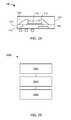
- FIG. 1is a bottom plan view of a dual molded multi-chip package system in an embodiment of the present invention
- FIG. 2is a cross-sectional view of the dual molded multi-chip package system along a line segment 2 - 2 of FIG. 1 ;
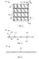
- FIG. 3is a top view of a lead frame in an embodiment of the present invention.
- FIG. 4is a first cross-sectional view of the lead frame along a line segment 4 - 4 of FIG. 3 ;
- FIG. 5is a second cross-sectional view of the lead frame along a line segment 5 - 5 of FIG. 3 ;
- FIG. 6is the structure of FIG. 3 in a taping phase
- FIG. 7is a cross-sectional view of the structure of FIG. 6 along a line segment 7 - 7 of FIG. 6 ;
- FIG. 8is the structure of FIG. 6 in a die-attaching phase
- FIG. 9is a cross-sectional view of the structure of FIG. 8 along a line segment 9 - 9 of FIG. 8 ;
- FIG. 10is the structure of FIG. 8 in a first molding phase
- FIG. 11is a cross-sectional view of the structure of FIG. 10 along a line segment 11 - 11 of FIG. 10 ;
- FIG. 12is the structure of FIG. 10 in a de-taping phase
- FIG. 13is a bottom view of FIG. 12 ;
- FIG. 14is a cross-sectional view of the structure of FIG. 12 along a line segment 14 - 14 of FIG. 12 ;
- FIG. 15is the structure of FIG. 13 in a mounting phase
- FIG. 16is the structure of FIG. 15 in a route-forming phase
- FIG. 17is the structure of FIG. 16 in a masking phase
- FIG. 18is the structure of FIG. 17 in a strip-forming phase
- FIG. 19is a bottom view of FIG. 18 ;
- FIG. 20is a cross-sectional view of the structure of FIG. 18 along a line segment 20 - 20 of FIG. 18 ;
- FIG. 21is the structure of FIG. 20 in a device-stacking phase
- FIG. 22is the structure of FIG. 21 in a device-connecting phase
- FIG. 23is the structure of FIG. 22 in a second molding phase
- FIG. 24is the structure of FIG. 23 in a singulating phase.
- FIG. 25is a flow chart of a dual molded multi-chip package system for manufacture of the dual molded multi-chip package system in an embodiment of the present invention.
- the term “horizontal” as used hereinis defined as a plane parallel to the plane or surface of the integrated circuit, regardless of its orientation.
- the term “vertical”refers to a direction perpendicular to the horizontal as just defined. Terms, such as “above”, “below”, “bottom”, “top”, “side” (as in “sidewall”), “higher”, “lower”, “upper”, “over”, and “under”, are defined with respect to the horizontal plane.
- the term “on”means there is direct contact among elements.
- processingas used herein includes deposition of material, patterning, exposure, development, etching, cleaning, molding, and/or removal of the material or as required in forming a described structure.
- systemas used herein means and refers to the method and to the apparatus of the present invention in accordance with the context in which the term is used.
- FIG. 1therein is shown a bottom plan view of a dual molded multi-chip package system 100 in an embodiment of the present invention.
- the bottom plan viewdepicts the dual molded multi-chip package system 100 without a solder mask that will be described in FIG. 17 .
- the bottom plan viewdepicts a first integrated circuit die 102 and a second integrated circuit die 104 connected by traces 106 , such as routing traces.
- the traces 106are entirely planar and in direct contact with a bottom surface of the first encapsulation 112 .
- the traces 106are further depicted as exposed to the external environment not internal to the first encapsulation 112 .
- the traces 106connect the first integrated circuit die 102 and the second integrated circuit die 104 with external interconnects 108 .
- the external interconnects 108are depicted exposed to the external environment, and can be a solder ball or solder bumps, that are formed in direct contact with an end of the traces 106 .
- the traces 106further connect between and are in direct contact with the first integrated circuit die 102 and leads 110 .
- the first integrated circuit die 102 and the second integrated circuit die 104are both between the leads 110 .
- a first encapsulation 112such as an epoxy mold compound, is around the first integrated circuit die 102 , the second integrated circuit die 104 , and the traces 106 .
- the first encapsulation 112exposes a first active side 114 of the first integrated circuit die 102 and a second active side 116 of the second integrated circuit die 104 .
- FIG. 2therein is shown a cross-sectional view of the dual molded multi-chip package system 100 along a line segment 2 - 2 of FIG. 1 .
- the cross-sectional viewdepicts the dual molded multi-chip package system 100 including an embedded integrated circuit package system 202 .
- the embedded integrated circuit package system 202has the first integrated circuit die 102 , the second integrated circuit die 104 of FIG. 1 , and the leads 110 partially encapsulated in the first encapsulation 112 .
- the first active side 114 and the second active side 116 of FIG. 1are substantially coplanar.
- Each of the leads 110has an extension 208 , a first surface 210 , and a second surface 212 .
- the extension 208may be a lead finger of the leads 110 .
- the first surface 210is the surface including the extension 208 .
- the second surface 212is the opposite surface of the first surface 210 .
- the cross-sectional viewdepicts the first encapsulation 112 partially covering the leads 110 , the extension 208 , and the first integrated circuit die 102 .
- the first encapsulation 112exposes the first surface 210 , the second surface 212 , and periphery sides 214 of the leads 110 .
- the first encapsulation 112 , the leads 110 , the extension 208 , the first integrated circuit die 102 , the second integrated circuit die 104 , and the traces 106are over the external interconnects 108 .
- the leads 110 with the extension 208may form mold locks improving the dual molded multi-chip package system 100 in moisture sensitivity level (MSL) test.
- the second surface 212 and the periphery sides 214may be used for further connections to the next system level (not shown), such as another integrated circuit package system, another dual molded multi-chip package system, or a printed circuit board.
- the cross-sectional viewdepicts the extension 208 substantially the same between the leads 110 , although it is understood that the extension 208 may differ.
- a semiconductor device 216such as an integrated circuit die, is over the embedded integrated circuit package system 202 .
- Internal interconnects 218such as bond wires or ribbon bond wires, are between the semiconductor device 216 and the leads 110 .
- the extension 208 or the first surface 210may serve as bond pads for the internal interconnects 218 .
- the leads 110may serve as communication structures between the semiconductor device 216 and the first integrated circuit die 102 as well as between the semiconductor device 216 and the second integrated circuit die 104 .
- the leads 110are not traditional electrical vias, wherein the electrical vias are defined as electrical conduction structures between different conduction levels and surrounded by insulating material, such as a dielectric.
- a second encapsulation 220covers the semiconductor device 216 , the internal interconnects 218 , the first surface 210 , and a surface of the first encapsulation 112 approximate to the first surface 210 .
- the cross-sectional viewdepicts encapsulation sides 222 of the second encapsulation 220 and the periphery sides 214 of the leads 110 as substantially coplanar.
- the encapsulation sides 222 and the periphery sides 214are shown as substantially coplanar, although it is understood that the encapsulation sides 222 and the periphery sides 214 may not be coplanar, such as the encapsulation sides 222 may have an angled configuration.
- FIG. 3therein is shown a top view of a lead frame 300 in an embodiment of the present invention.
- the lead frame 300has an array of window frames 302 , strip lines 304 , and holes 306 .
- the lead frame 300is used to form the dual molded multi-chip package system 100 of FIG. 1 .
- Each of the window frames 302has an opening 308 in a frame 310 and a number of instances of the extension 208 extending into the opening 308 at opposite sides of the frame 310 .
- the window frames 302 , the opening 308 , and the extension 208may be formed by a number of different processes, such as stamping, etching, half etching, or preformed.
- the extension 208is shown not extending from side to side of the frame 310 , although it is understood that the extension 208 may extend from side to side of the frame 310 .
- the holes 306are at the corners of the lead frame 300 and may be serve as alignment guides for further processing of the lead frame 300 .
- the holes 306may be formed by a number of different processes, such as stamping, etching, or preformed.
- the holes 306are shown at the corners of the lead frame 300 , although it is understood that the holes 306 may be at different locations of the lead frame 300 .
- the lead frame 300has the holes 306 as potential alignment guides although it is understood that the lead frame 300 may have different alignment structures, such as notches along the sides of the lead frame 300 .
- the strip lines 304are between rows of the window frames 302 .
- the strip lines 304may be formed by a number of different processes, such as half etching.
- the top viewdepicts the strip lines 304 delineating rows of the window frames 302 , although it is understood that the strip lines 304 may delineate columns of the window frames 302 .
- FIG. 4therein is shown a first cross-sectional view of the lead frame 300 along a line segment 4 - 4 of FIG. 3 .
- the first cross-sectional viewdepicts the window frames 302 having the frame 310 .
- the leads 110 and the extension 208 of each of the leads 110extend from the frame 310 into the opening 308 . Instances of the extension 208 at the opposite sides of the frame 310 are along a top side 402 of the lead frame 300 .
- the instances of the extension 208are shown at the top side 402 , although it is understood that the instances of the extension 208 may not be at the top side 402 , such as a bottom side 404 of the frame 310 . Also for illustrative purposes, the instances of the extension 208 are shown at the top side 402 , although it is understood that the instances of the extension 208 may not be along the same side of the frame 310 .
- FIG. 5therein is shown a second cross-sectional view of the lead frame 300 along a line segment 5 - 5 of FIG. 3 .
- the second cross-sectional viewshows the strip lines 304 as recesses in the lead frame 300 .
- the strip lines 304do not affect the structural rigidity of the lead frame 300 to withstand handling of the lead frame 300 for further processing.
- FIG. 6therein is shown the structure of FIG. 3 in a taping phase.
- a tape 602such as a coverlay tape, is attached on the bottom side 404 of FIG. 4 of the lead frame 300 .
- the tape 602is visible through the opening 308 .
- the strip lines 304are shown not affected by the tape 602 .
- FIG. 7is a cross-sectional view of the structure of FIG. 6 along a line segment 7 - 7 of FIG. 6 .
- the tape 602 along the bottom side 404 of the lead frame 300forms a substantially coplanar surface in the opening 308 and the frame 310 .
- the top side 402is shown as unaffected by the tape 602 .
- FIG. 8therein is shown the structure of FIG. 6 in a die-attaching phase.
- the first integrated circuit die 102 and the second integrated circuit die 104are placed in the opening 308 in each of the window frames 302 and over the tape 602 .
- the first integrated circuit die 102 having a first non-active side 802 and the second integrated circuit die 104 having a second non-active side 804are facing down such that the first non-active side 802 and the second non-active side 804 are shown and not facing the tape 602 .
- the extension 208do not impede the first integrated circuit die 102 and the second integrated circuit die 104 in the opening 308 .
- FIG. 9therein is shown a cross-sectional view of the structure of FIG. 8 along a line segment 9 - 9 of FIG. 8 .
- the first integrated circuit die 102 of FIG. 8 having the first active side 114 of FIG. 1 and the second integrated circuit die 104 having the second active side 116are facing down in the opening 308 .
- the first active side 114 and the second active side 116face and are on the tape 602 .
- the first active side 114 , the second active side 116 , and the bottom side 404are substantially coplanar.
- the top side 402is above the first non-active side 802 and the second non-active side 804 .
- FIG. 10therein is shown the structure of FIG. 8 in a first molding phase.
- a molding compoundsuch as an epoxy mold compound, fills the opening 308 of each of the window frames 302 forming the first encapsulation 112 .
- the first encapsulation 112outlines the opening 308 and exposes the instances of the extension 208 of the frame 310 .
- the first encapsulation 112may be formed by a number of different processes, such as screen print or transfer molding.
- a planarization processmay be performed to expose the extension 208 .
- FIG. 11therein is shown a cross-sectional view of the structure of FIG. 10 along a line segment 11 - 11 of FIG. 10 .
- the cross-sectional viewdepicts the tape 602 attached to the bottom side 404 .
- the tape 602helps shape the first encapsulation 112 to be coplanar with the first active side 114 of FIG. 1 and the second active side 116 .
- the first encapsulation 112fills the opening 308 in the lead frame 300 and covers the first non-active side 802 of FIG. 8 and the second non-active side 804 .
- the first encapsulation 112exposes the extension 208 and the top side 402 .
- FIG. 12therein is shown the structure of FIG. 10 in a de-taping phase.
- the top view showndepicts the top side 402 and similar to that shown in FIG. 10 .
- the first encapsulation 112is in the opening 308 of each of the window frames 302 and exposes the instances of the extension 208 .
- the holes 306are not filled by the first encapsulation 112 .
- the strip lines 304are shown not affected by the first encapsulation 112 .
- FIG. 13therein is shown a bottom view of FIG. 12 .
- the bottom viewdepicts the tape 602 of FIG. 11 removed.
- the opening 308has the first encapsulation 112 , the first integrated circuit die 102 , the second integrated circuit die 104 , and the leads 110 .
- the first encapsulation 112exposes the first active side 114 , the second active side 116 , and the leads 110 .
- FIG. 14therein is shown a cross-sectional view of the structure of FIG. 12 along a line segment 14 - 14 of FIG. 12 .
- the cross-sectional viewdepicts the first encapsulation 112 exposing the second active side 116 .
- the first active side 114 of FIG. 1 , the second active side 116 , the bottom side 404 , the leads 110 , and the first encapsulation 112 along the bottom side 404are substantially coplanar.
- the first encapsulation 112fills the opening 308 covering the first integrated circuit die 102 and the second integrated circuit die 104 excluding the first active side 114 and the second active side 116 .
- the first encapsulation 112also exposes the extension 208 and the top side 402 .
- FIG. 15therein is shown the structure of FIG. 13 in a mounting phase.
- the structure of FIG. 13is mounted on a support structure 1402 , such as a wafer carrier, with the bottom side 404 facing up.
- the support structure 1402helps keeps the structure of FIG. 13 planar for further processing.
- the lead frame 300has the first integrated circuit die 102 and the second integrated circuit die 104 exposed and in the first encapsulation 112 .
- the first encapsulation 112also exposes the leads 110 from the lead frame 300 .
- the holes 306may be used with pins (not shown) from the support structure 1402 for aligning the lead frame 300 .
- Bond sites 1602 and the traces 106are formed on the first encapsulation 112 .
- the traces 106connect the first integrated circuit die 102 and the second integrated circuit die 104 .
- the traces 106also connect both the first integrated circuit die 102 and the second integrated circuit die 104 with the bond sites 1602 and the leads 110 .
- the bond sites 1602 and the traces 106may be formed by a number of different processes, such as depositing conductive materials.
- the bond sites 1602are shown at the periphery of the first encapsulation 112 , although it is understood that the bond sites 1602 may be at other locations, such as at an interior region of the first encapsulation 112 .
- the traces 106are shown as routing for the first integrated circuit die 102 , the second integrated circuit die 104 , the leads 110 , and the bond sites 1602 , although it is understood that the traces 106 may provide additional functions, such as a redistribution structure or forming a circuit element.
- the top side 402 of FIG. 12may also have the traces 106 and the bond sites 1602 .
- FIG. 17therein is the structure of FIG. 16 in a masking phase.
- a solder mask 1702is formed over the structure of FIG. 16 .
- the solder mask 1702has alignment guides 1704 that align with the holes 306 of FIG. 12 .
- the solder mask 1702exposes the bond sites 1602 for further processing.
- FIG. 18therein is shown the structure of FIG. 17 in a strip-forming phase.
- the structure of FIG. 17undergoes a singulation process forming a lead frame strip 1802 .
- the lead frame 300 shown in FIG. 15is singulated at the strip lines 304 shown in FIG. 3 .
- the singulation processmay be performed by a number of different processes, such as sawing or punching.
- the top side 402 of the lead frame strip 1802depicts the window frames 302 with the opening 308 .
- the first encapsulation 112is in the opening 308 and exposing the extension 208 .
- FIG. 19therein is shown a bottom view of FIG. 18 .
- the bottom viewdepicts the lead frame strip 1802 with the solder mask 1702 exposing the bond sites 1602 .
- FIG. 20therein is shown a cross-sectional view of the structure of FIG. 18 along a line segment 20 - 20 of FIG. 18 .
- the cross-sectional viewdepicts the lead frame strip 1802 with the first encapsulation 112 exposing the second active side 116 .
- the first active side 114 of FIG. 1 , the second active side 116 , the bottom side 404 , the leads 110 , and the first encapsulation 112 along the bottom side 404are substantially coplanar.
- the first encapsulation 112fills the opening 308 covering the first integrated circuit die 102 of FIG. 1 and the second integrated circuit die 104 excluding the first active side 114 and the second active side 116 .
- the first encapsulation 112also exposes the extension 208 and the top side 402 .
- FIG. 21therein is shown the structure of FIG. 20 in a device-stacking phase.
- the semiconductor device 216mounts over the first encapsulation 112 along the top side 402 of the lead frame strip 1802 .
- the semiconductor device 216mounts on the first encapsulation 112 with an adhesive 2122 , such as a die-attach adhesive, in each of the window frames 302 .
- the adhesive 2122 and the semiconductor device 216do not impede or contaminate the top side 402 of the extension 208 and the leads 110 .
- the bottom side 404 of the lead frame strip 1802is shown as unaffected.
- FIG. 22therein is shown the structure of FIG. 21 in a device-connecting phase.
- the lead frame strip 1802undergoes an electrical connecting process.
- the internal interconnects 218attach the semiconductor device 216 and the extension 208 or the top side 402 of the leads 110 .
- the internal interconnects 218may be attached by a number of different processes, such a wire bonding.
- the internal interconnects 218may form electrical connections between the semiconductor device 216 and the first integrated circuit die 102 of FIG. 1 as well as the second integrated circuit die 104 .
- the electrical connectionsare formed with the extension 208 , the leads 110 , the bond sites 1602 of FIG. 16 , and the traces 106 of FIG. 16 without traditional electrical vias (not shown).
- FIG. 23therein is shown the structure of FIG. 22 in a second molding phase.
- a molding compoundsuch as an epoxy molding compound, covers the top side 402 of the lead frame strip 1802 forming the second encapsulation 220 .
- the second encapsulation 220covers the semiconductor device 216 and the internal interconnects 218 .
- the external interconnects 108attach to the bond sites 1602 of FIG. 16 exposed in the solder mask 1702 of FIG. 19 .
- FIG. 24therein is shown the structure of FIG. 23 in a singulating phase.
- the singulationmay be performed by a number of different processes, such as sawing.
- the structure of FIG. 23undergoes a singulating process forming the dual molded multi-chip package system 100 .
- the cross-sectional viewdepicts singulating process forming the periphery sides 214 of the leads 110 coplanar with the encapsulation sides 222 of the second encapsulation 220 .
- the semiconductor device 216 , the internal interconnects 218 , and the second encapsulation 220are over the embedded integrated circuit package system 202 .
- the system 2500includes forming an embedded integrated circuit package system having a first encapsulation partially covering a first integrated circuit die and a lead connected thereto in a block 2502 ; mounting a semiconductor device over the first encapsulation and connected to the lead in a block 2504 ; and forming a second encapsulation over the semiconductor device and the embedded integrated circuit package system in a block 2506 .
- Yet another important aspect of the present inventionis that it valuably supports and services the historical trend of reducing costs, simplifying systems, and increasing performance.
- the dual molded multi-chip package system of the present inventionfurnishes important and heretofore unknown and unavailable solutions, capabilities, and functional aspects for improving reliability in systems.
- the resulting processes and configurationsare straightforward, cost-effective, uncomplicated, highly versatile, and effective, can be implemented by adapting known technologies, and are thus readily suited for efficiently and economically manufacturing integrated circuit package devices.
Landscapes
- Engineering & Computer Science (AREA)
- Microelectronics & Electronic Packaging (AREA)
- Power Engineering (AREA)
- Computer Hardware Design (AREA)
- Physics & Mathematics (AREA)
- Condensed Matter Physics & Semiconductors (AREA)
- General Physics & Mathematics (AREA)
- Manufacturing & Machinery (AREA)
- Structures Or Materials For Encapsulating Or Coating Semiconductor Devices Or Solid State Devices (AREA)
Abstract
Description
Claims (20)
Priority Applications (5)
| Application Number | Priority Date | Filing Date | Title |
|---|---|---|---|
| US11/618,806US8178982B2 (en) | 2006-12-30 | 2006-12-30 | Dual molded multi-chip package system |
| TW096149652ATWI441265B (en) | 2006-12-30 | 2007-12-24 | Dual molded multi-chip package system |
| JP2007339497AJP5348632B2 (en) | 2006-12-30 | 2007-12-28 | Dual mold multichip package system and manufacturing method thereof |
| KR1020070140692AKR101521254B1 (en) | 2006-12-30 | 2007-12-28 | Double-molded multi-chip package system |
| US13/443,067US8558399B2 (en) | 2006-12-30 | 2012-04-10 | Dual molded multi-chip package system |
Applications Claiming Priority (1)
| Application Number | Priority Date | Filing Date | Title |
|---|---|---|---|
| US11/618,806US8178982B2 (en) | 2006-12-30 | 2006-12-30 | Dual molded multi-chip package system |
Related Child Applications (1)
| Application Number | Title | Priority Date | Filing Date |
|---|---|---|---|
| US13/443,067ContinuationUS8558399B2 (en) | 2006-12-30 | 2012-04-10 | Dual molded multi-chip package system |
Publications (2)
| Publication Number | Publication Date |
|---|---|
| US20080157402A1 US20080157402A1 (en) | 2008-07-03 |
| US8178982B2true US8178982B2 (en) | 2012-05-15 |
Family
ID=39582767
Family Applications (2)
| Application Number | Title | Priority Date | Filing Date |
|---|---|---|---|
| US11/618,806Active2027-03-02US8178982B2 (en) | 2006-12-30 | 2006-12-30 | Dual molded multi-chip package system |
| US13/443,067ActiveUS8558399B2 (en) | 2006-12-30 | 2012-04-10 | Dual molded multi-chip package system |
Family Applications After (1)
| Application Number | Title | Priority Date | Filing Date |
|---|---|---|---|
| US13/443,067ActiveUS8558399B2 (en) | 2006-12-30 | 2012-04-10 | Dual molded multi-chip package system |
Country Status (4)
| Country | Link |
|---|---|
| US (2) | US8178982B2 (en) |
| JP (1) | JP5348632B2 (en) |
| KR (1) | KR101521254B1 (en) |
| TW (1) | TWI441265B (en) |
Cited By (2)
| Publication number | Priority date | Publication date | Assignee | Title |
|---|---|---|---|---|
| US20120049375A1 (en)* | 2010-08-31 | 2012-03-01 | Thorsten Meyer | Method and system for routing electrical connections of semiconductor chips |
| US9034692B2 (en)* | 2011-03-21 | 2015-05-19 | Stats Chippac Ltd. | Integrated circuit packaging system with a flip chip and method of manufacture thereof |
Families Citing this family (18)
| Publication number | Priority date | Publication date | Assignee | Title |
|---|---|---|---|---|
| TW200802751A (en)* | 2005-11-01 | 2008-01-01 | Koninkl Philips Electronics Nv | An air cavity package for a semiconductor die and methods of forming the air cavity package |
| US8178982B2 (en) | 2006-12-30 | 2012-05-15 | Stats Chippac Ltd. | Dual molded multi-chip package system |
| TWI360207B (en) | 2007-10-22 | 2012-03-11 | Advanced Semiconductor Eng | Chip package structure and method of manufacturing |
| US7888184B2 (en)* | 2008-06-20 | 2011-02-15 | Stats Chippac Ltd. | Integrated circuit packaging system with embedded circuitry and post, and method of manufacture thereof |
| US8076786B2 (en)* | 2008-07-11 | 2011-12-13 | Advanced Semiconductor Engineering, Inc. | Semiconductor package and method for packaging a semiconductor package |
| US7842542B2 (en) | 2008-07-14 | 2010-11-30 | Stats Chippac, Ltd. | Embedded semiconductor die package and method of making the same using metal frame carrier |
| US8354304B2 (en)* | 2008-12-05 | 2013-01-15 | Stats Chippac, Ltd. | Semiconductor device and method of forming conductive posts embedded in photosensitive encapsulant |
| US7993941B2 (en)* | 2008-12-05 | 2011-08-09 | Stats Chippac, Ltd. | Semiconductor package and method of forming Z-direction conductive posts embedded in structurally protective encapsulant |
| JP5238523B2 (en) | 2009-01-13 | 2013-07-17 | 株式会社日立国際電気 | Moving picture encoding apparatus, moving picture decoding apparatus, and moving picture decoding method |
| US8003445B2 (en)* | 2009-03-26 | 2011-08-23 | Stats Chippac Ltd. | Integrated circuit packaging system with z-interconnects having traces and method of manufacture thereof |
| US8569894B2 (en) | 2010-01-13 | 2013-10-29 | Advanced Semiconductor Engineering, Inc. | Semiconductor package with single sided substrate design and manufacturing methods thereof |
| TWI411075B (en) | 2010-03-22 | 2013-10-01 | Advanced Semiconductor Eng | Semiconductor package and manufacturing method thereof |
| US8409978B2 (en) | 2010-06-24 | 2013-04-02 | Stats Chippac, Ltd. | Semiconductor device and method of forming vertically offset bond on trace interconnect structure on leadframe |
| US8753926B2 (en)* | 2010-09-14 | 2014-06-17 | Qualcomm Incorporated | Electronic packaging with a variable thickness mold cap |
| US9406658B2 (en) | 2010-12-17 | 2016-08-02 | Advanced Semiconductor Engineering, Inc. | Embedded component device and manufacturing methods thereof |
| TWI590392B (en)* | 2015-08-03 | 2017-07-01 | 矽品精密工業股份有限公司 | Electronic package and method of manufacture thereof |
| JP7746888B2 (en)* | 2022-03-14 | 2025-10-01 | 住友電気工業株式会社 | Semiconductor device and manufacturing method thereof |
| CN117832190A (en)* | 2022-09-28 | 2024-04-05 | 星科金朋私人有限公司 | Integrated package and method of manufacturing the same |
Citations (14)
| Publication number | Priority date | Publication date | Assignee | Title |
|---|---|---|---|---|
| US5239198A (en)* | 1989-09-06 | 1993-08-24 | Motorola, Inc. | Overmolded semiconductor device having solder ball and edge lead connective structure |
| US5353498A (en) | 1993-02-08 | 1994-10-11 | General Electric Company | Method for fabricating an integrated circuit module |
| US6159767A (en) | 1996-05-20 | 2000-12-12 | Epic Technologies, Inc. | Single chip modules, repairable multichip modules, and methods of fabrication thereof |
| US6300679B1 (en)* | 1998-06-01 | 2001-10-09 | Semiconductor Components Industries, Llc | Flexible substrate for packaging a semiconductor component |
| US6309912B1 (en) | 2000-06-20 | 2001-10-30 | Motorola, Inc. | Method of interconnecting an embedded integrated circuit |
| US20040080025A1 (en) | 2002-09-17 | 2004-04-29 | Shinko Electric Industries Co., Ltd. | Lead frame, method of manufacturing the same, and semiconductor device manufactured with the same |
| US20050006737A1 (en) | 2002-04-29 | 2005-01-13 | Shafidul Islam | Partially patterned lead frames and methods of making and using the same in semiconductor packaging |
| US20050184377A1 (en) | 2004-01-30 | 2005-08-25 | Shinko Electric Industries Co., Ltd. | Semiconductor device and method of manufacturing the same |
| US6946325B2 (en) | 2003-03-14 | 2005-09-20 | Micron Technology, Inc. | Methods for packaging microelectronic devices |
| US20050269681A1 (en) | 2001-10-18 | 2005-12-08 | Matsushita Electric Industrial Co., Ltd. | Component built-in module and method for producing the same |
| US7084513B2 (en) | 2001-12-07 | 2006-08-01 | Fujitsu Limited | Semiconductor device having a plurality of semiconductor chips and method for manufacturing the same |
| US20060170098A1 (en) | 2005-02-01 | 2006-08-03 | Shih-Ping Hsu | Module structure having embedded chips |
| US20060197210A1 (en)* | 2005-03-04 | 2006-09-07 | Hyun-Ki Kim | Stack semiconductor package formed by multiple molding and method of manufacturing the same |
| US7208345B2 (en)* | 2005-05-11 | 2007-04-24 | Infineon Technologies Ag | Method of manufacturing a semiconductor device comprising stacked chips and a corresponding semiconductor device |
Family Cites Families (15)
| Publication number | Priority date | Publication date | Assignee | Title |
|---|---|---|---|---|
| KR100372153B1 (en)* | 1995-04-05 | 2003-06-19 | 내셔널 세미콘덕터 코포레이션 | Multi-layer lead frame |
| US20010052647A1 (en) | 1998-05-07 | 2001-12-20 | 3M Innovative Properties Company | Laminated integrated circuit package |
| KR100302593B1 (en)* | 1998-10-24 | 2001-09-22 | 김영환 | Semiconductor package and fabricating method thereof |
| US6078505A (en) | 1999-05-14 | 2000-06-20 | Triquint Semiconductor, Inc. | Circuit board assembly method |
| JP3497775B2 (en)* | 1999-08-23 | 2004-02-16 | 松下電器産業株式会社 | Semiconductor device |
| JP2001320015A (en)* | 2000-05-12 | 2001-11-16 | Sony Corp | Semiconductor device and its manufacturing method |
| JP2002134653A (en)* | 2000-10-23 | 2002-05-10 | Matsushita Electric Ind Co Ltd | Semiconductor device and manufacturing method thereof |
| US7548430B1 (en)* | 2002-05-01 | 2009-06-16 | Amkor Technology, Inc. | Buildup dielectric and metallization process and semiconductor package |
| JP2005317903A (en)* | 2004-03-31 | 2005-11-10 | Alps Electric Co Ltd | Circuit component module, circuit component module stack, recording medium and manufacturing method of them |
| JP2006120943A (en)* | 2004-10-22 | 2006-05-11 | Shinko Electric Ind Co Ltd | Chip built-in substrate and its manufacturing method |
| JP2006295051A (en)* | 2005-04-14 | 2006-10-26 | Sony Corp | Semiconductor device and its manufacturing method |
| US7408254B1 (en)* | 2005-08-26 | 2008-08-05 | Amkor Technology Inc | Stack land grid array package and method for manufacturing the same |
| US8178982B2 (en) | 2006-12-30 | 2012-05-15 | Stats Chippac Ltd. | Dual molded multi-chip package system |
| US7868445B2 (en) | 2007-06-25 | 2011-01-11 | Epic Technologies, Inc. | Integrated structures and methods of fabrication thereof with fan-out metallization on a chips-first chip layer |
| US7888184B2 (en) | 2008-06-20 | 2011-02-15 | Stats Chippac Ltd. | Integrated circuit packaging system with embedded circuitry and post, and method of manufacture thereof |
- 2006
- 2006-12-30USUS11/618,806patent/US8178982B2/enactiveActive
- 2007
- 2007-12-24TWTW096149652Apatent/TWI441265B/enactive
- 2007-12-28JPJP2007339497Apatent/JP5348632B2/enactiveActive
- 2007-12-28KRKR1020070140692Apatent/KR101521254B1/enactiveActive
- 2012
- 2012-04-10USUS13/443,067patent/US8558399B2/enactiveActive
Patent Citations (14)
| Publication number | Priority date | Publication date | Assignee | Title |
|---|---|---|---|---|
| US5239198A (en)* | 1989-09-06 | 1993-08-24 | Motorola, Inc. | Overmolded semiconductor device having solder ball and edge lead connective structure |
| US5353498A (en) | 1993-02-08 | 1994-10-11 | General Electric Company | Method for fabricating an integrated circuit module |
| US6159767A (en) | 1996-05-20 | 2000-12-12 | Epic Technologies, Inc. | Single chip modules, repairable multichip modules, and methods of fabrication thereof |
| US6300679B1 (en)* | 1998-06-01 | 2001-10-09 | Semiconductor Components Industries, Llc | Flexible substrate for packaging a semiconductor component |
| US6309912B1 (en) | 2000-06-20 | 2001-10-30 | Motorola, Inc. | Method of interconnecting an embedded integrated circuit |
| US20050269681A1 (en) | 2001-10-18 | 2005-12-08 | Matsushita Electric Industrial Co., Ltd. | Component built-in module and method for producing the same |
| US7084513B2 (en) | 2001-12-07 | 2006-08-01 | Fujitsu Limited | Semiconductor device having a plurality of semiconductor chips and method for manufacturing the same |
| US20050006737A1 (en) | 2002-04-29 | 2005-01-13 | Shafidul Islam | Partially patterned lead frames and methods of making and using the same in semiconductor packaging |
| US20040080025A1 (en) | 2002-09-17 | 2004-04-29 | Shinko Electric Industries Co., Ltd. | Lead frame, method of manufacturing the same, and semiconductor device manufactured with the same |
| US6946325B2 (en) | 2003-03-14 | 2005-09-20 | Micron Technology, Inc. | Methods for packaging microelectronic devices |
| US20050184377A1 (en) | 2004-01-30 | 2005-08-25 | Shinko Electric Industries Co., Ltd. | Semiconductor device and method of manufacturing the same |
| US20060170098A1 (en) | 2005-02-01 | 2006-08-03 | Shih-Ping Hsu | Module structure having embedded chips |
| US20060197210A1 (en)* | 2005-03-04 | 2006-09-07 | Hyun-Ki Kim | Stack semiconductor package formed by multiple molding and method of manufacturing the same |
| US7208345B2 (en)* | 2005-05-11 | 2007-04-24 | Infineon Technologies Ag | Method of manufacturing a semiconductor device comprising stacked chips and a corresponding semiconductor device |
Cited By (3)
| Publication number | Priority date | Publication date | Assignee | Title |
|---|---|---|---|---|
| US20120049375A1 (en)* | 2010-08-31 | 2012-03-01 | Thorsten Meyer | Method and system for routing electrical connections of semiconductor chips |
| US8598709B2 (en)* | 2010-08-31 | 2013-12-03 | Infineon Technologies Ag | Method and system for routing electrical connections of semiconductor chips |
| US9034692B2 (en)* | 2011-03-21 | 2015-05-19 | Stats Chippac Ltd. | Integrated circuit packaging system with a flip chip and method of manufacture thereof |
Also Published As
| Publication number | Publication date |
|---|---|
| TW200836272A (en) | 2008-09-01 |
| TWI441265B (en) | 2014-06-11 |
| JP2008166816A (en) | 2008-07-17 |
| US8558399B2 (en) | 2013-10-15 |
| US20120193805A1 (en) | 2012-08-02 |
| KR101521254B1 (en) | 2015-05-18 |
| US20080157402A1 (en) | 2008-07-03 |
| JP5348632B2 (en) | 2013-11-20 |
| KR20080063197A (en) | 2008-07-03 |
Similar Documents
| Publication | Publication Date | Title |
|---|---|---|
| US8178982B2 (en) | Dual molded multi-chip package system | |
| US7741707B2 (en) | Stackable integrated circuit package system | |
| US8163600B2 (en) | Bridge stack integrated circuit package-on-package system | |
| US7659609B2 (en) | Integrated circuit package-in-package system with carrier interposer | |
| US7566966B2 (en) | Integrated circuit package-on-package system with anti-mold flash feature | |
| US8084849B2 (en) | Integrated circuit package system with offset stacking | |
| US7368319B2 (en) | Stacked integrated circuit package-in-package system | |
| US8035207B2 (en) | Stackable integrated circuit package system with recess | |
| US8536692B2 (en) | Mountable integrated circuit package system with mountable integrated circuit die | |
| US7535086B2 (en) | Integrated circuit package-on-package stacking system | |
| US7871861B2 (en) | Stacked integrated circuit package system with intra-stack encapsulation | |
| US8143711B2 (en) | Integrated circuit package system with offset stacking and anti-flash structure | |
| US7687897B2 (en) | Mountable integrated circuit package-in-package system with adhesive spacing structures | |
| US7956449B2 (en) | Stacked integrated circuit package system | |
| US20090140408A1 (en) | Integrated circuit package-on-package system with stacking via interconnect | |
| US7985628B2 (en) | Integrated circuit package system with interconnect lock | |
| US8258614B2 (en) | Integrated circuit package system with package integration | |
| US8847413B2 (en) | Integrated circuit package system with leads having multiple sides exposed | |
| US7750451B2 (en) | Multi-chip package system with multiple substrates | |
| US8183675B2 (en) | Integrated circuit package-on-package system with anti-mold flash feature | |
| US8304898B2 (en) | Integrated circuit package system with overhang film |
Legal Events
| Date | Code | Title | Description |
|---|---|---|---|
| AS | Assignment | Owner name:STATS CHIPPAC LTD., SINGAPORE Free format text:ASSIGNMENT OF ASSIGNORS INTEREST;ASSIGNORS:RAMAKRISHNA, KAMBHAMPATI;SHIM, IL KWON;CHOW, SENG GUAN;REEL/FRAME:018819/0294;SIGNING DATES FROM 20070102 TO 20070105 Owner name:STATS CHIPPAC LTD., SINGAPORE Free format text:ASSIGNMENT OF ASSIGNORS INTEREST;ASSIGNORS:RAMAKRISHNA, KAMBHAMPATI;SHIM, IL KWON;CHOW, SENG GUAN;SIGNING DATES FROM 20070102 TO 20070105;REEL/FRAME:018819/0294 | |
| STCF | Information on status: patent grant | Free format text:PATENTED CASE | |
| AS | Assignment | Owner name:CITICORP INTERNATIONAL LIMITED, AS COMMON SECURITY AGENT, HONG KONG Free format text:SECURITY INTEREST;ASSIGNORS:STATS CHIPPAC, INC.;STATS CHIPPAC LTD.;REEL/FRAME:036288/0748 Effective date:20150806 Owner name:CITICORP INTERNATIONAL LIMITED, AS COMMON SECURITY Free format text:SECURITY INTEREST;ASSIGNORS:STATS CHIPPAC, INC.;STATS CHIPPAC LTD.;REEL/FRAME:036288/0748 Effective date:20150806 | |
| FPAY | Fee payment | Year of fee payment:4 | |
| AS | Assignment | Owner name:STATS CHIPPAC PTE. LTE., SINGAPORE Free format text:CHANGE OF NAME;ASSIGNOR:STATS CHIPPAC LTD.;REEL/FRAME:038388/0036 Effective date:20160329 | |
| MAFP | Maintenance fee payment | Free format text:PAYMENT OF MAINTENANCE FEE, 8TH YEAR, LARGE ENTITY (ORIGINAL EVENT CODE: M1552); ENTITY STATUS OF PATENT OWNER: LARGE ENTITY Year of fee payment:8 | |
| AS | Assignment | Owner name:STATS CHIPPAC PTE. LTD. FORMERLY KNOWN AS STATS CH Free format text:RELEASE BY SECURED PARTY;ASSIGNOR:CITICORP INTERNATIONAL LIMITED, AS COMMON SECURITY AGENT;REEL/FRAME:051285/0318 Effective date:20190503 Owner name:STATS CHIPPAC, INC., CALIFORNIA Free format text:RELEASE BY SECURED PARTY;ASSIGNOR:CITICORP INTERNATIONAL LIMITED, AS COMMON SECURITY AGENT;REEL/FRAME:051285/0318 Effective date:20190503 Owner name:STATS CHIPPAC PTE. LTD. FORMERLY KNOWN AS STATS CHIPPAC LTD., SINGAPORE Free format text:RELEASE BY SECURED PARTY;ASSIGNOR:CITICORP INTERNATIONAL LIMITED, AS COMMON SECURITY AGENT;REEL/FRAME:051285/0318 Effective date:20190503 | |
| AS | Assignment | Owner name:JCET SEMICONDUCTOR (SHAOXING) CO., LTD., CHINA Free format text:ASSIGNMENT OF ASSIGNORS INTEREST;ASSIGNOR:STATS CHIPPAC PTE. LTD.;REEL/FRAME:051365/0680 Effective date:20191128 | |
| AS | Assignment | Owner name:STATS CHIPPAC PTE. LTE., SINGAPORE Free format text:CORRECT ERROR IN ASSIGNMENT NAME FROM STATS CHIPPAC PTE. LTE. TO STATS CHIPPAC PTE. LTD. (REEL: 38388 FRAME: 0036;ASSIGNOR:STATS CHIPPAC LTD.;REEL/FRAME:064789/0885 Effective date:20160329 | |
| AS | Assignment | Owner name:STATS CHIPPAC PTE. LTD., SINGAPORE Free format text:CORRECTIVE ASSIGNMENT TO CORRECT A TYPOGRAPHICAL ERROR ON THE COVER SHEET PREVIOUSLY RECORDED AT REEL: 038388 FRAME: 0036. ASSIGNOR(S) HEREBY CONFIRMS THE CHANGE OF NAME;ASSIGNOR:STATS CHIPPAC LTD.;REEL/FRAME:064834/0911 Effective date:20160329 Owner name:STATS CHIPPAC PTE. LTD., SINGAPORE Free format text:CORRECTIVE ASSIGNMENT TO CORRECT A TYPOGRAPHICAL ERROR ON THE COVER SHEET PREVIOUSLY RECORDED AT REEL: 064789 FRAME: 0885. ASSIGNOR(S) HEREBY CONFIRMS THE CORRECTIVE ASSIGNMENT;ASSIGNOR:STATS CHIPPAC LTD.;REEL/FRAME:064836/0363 Effective date:20160329 | |
| MAFP | Maintenance fee payment | Free format text:PAYMENT OF MAINTENANCE FEE, 12TH YEAR, LARGE ENTITY (ORIGINAL EVENT CODE: M1553); ENTITY STATUS OF PATENT OWNER: LARGE ENTITY Year of fee payment:12 |