US8178964B2 - Semiconductor device package with die receiving through-hole and dual build-up layers over both side-surfaces for WLP and method of the same - Google Patents
Semiconductor device package with die receiving through-hole and dual build-up layers over both side-surfaces for WLP and method of the sameDownload PDFInfo
- Publication number
- US8178964B2 US8178964B2US11/694,719US69471907AUS8178964B2US 8178964 B2US8178964 B2US 8178964B2US 69471907 AUS69471907 AUS 69471907AUS 8178964 B2US8178964 B2US 8178964B2
- Authority
- US
- United States
- Prior art keywords
- die
- substrate
- layer
- rdl
- dielectric layer
- Prior art date
- Legal status (The legal status is an assumption and is not a legal conclusion. Google has not performed a legal analysis and makes no representation as to the accuracy of the status listed.)
- Active, expires
Links
- 239000004065semiconductorSubstances0.000titleclaimsabstractdescription10
- 238000000034methodMethods0.000titledescription55
- 230000009977dual effectEffects0.000titledescription3
- 239000000758substrateSubstances0.000claimsabstractdescription87
- 239000000463materialSubstances0.000claimsabstractdescription48
- 238000009826distributionMethods0.000claimsabstractdescription8
- 239000002184metalSubstances0.000claimsdescription35
- 229910052751metalInorganic materials0.000claimsdescription35
- 239000004593EpoxySubstances0.000claimsdescription9
- 239000004642PolyimideSubstances0.000claimsdescription8
- 229920001721polyimidePolymers0.000claimsdescription8
- 239000010703siliconSubstances0.000claimsdescription7
- 229910052710siliconInorganic materials0.000claimsdescription7
- 239000011521glassSubstances0.000claimsdescription6
- 229910001020Au alloyInorganic materials0.000claimsdescription5
- 229920001296polysiloxanePolymers0.000claimsdescription5
- 239000000919ceramicSubstances0.000claimsdescription4
- KPUWHANPEXNPJT-UHFFFAOYSA-NdisiloxaneChemical class[SiH3]O[SiH3]KPUWHANPEXNPJT-UHFFFAOYSA-N0.000claimsdescription4
- 229920000642polymerPolymers0.000claimsdescription4
- 229920002050silicone resinPolymers0.000claimsdescription4
- 229910000881Cu alloyInorganic materials0.000claimsdescription3
- 229910000990Ni alloyInorganic materials0.000claimsdescription3
- 229910045601alloyInorganic materials0.000claimsdescription3
- 239000000956alloySubstances0.000claimsdescription3
- JYEUMXHLPRZUAT-UHFFFAOYSA-N1,2,3-triazineChemical compoundC1=CN=NN=C1JYEUMXHLPRZUAT-UHFFFAOYSA-N0.000claimsdescription2
- XQUPVDVFXZDTLT-UHFFFAOYSA-N1-[4-[[4-(2,5-dioxopyrrol-1-yl)phenyl]methyl]phenyl]pyrrole-2,5-dioneChemical compoundO=C1C=CC(=O)N1C(C=C1)=CC=C1CC1=CC=C(N2C(C=CC2=O)=O)C=C1XQUPVDVFXZDTLT-UHFFFAOYSA-N0.000claimsdescription2
- 229920003192poly(bis maleimide)Polymers0.000claimsdescription2
- 230000035882stressEffects0.000description11
- 229910000679solderInorganic materials0.000description9
- 230000001351cycling effectEffects0.000description8
- 238000012360testing methodMethods0.000description7
- XUIMIQQOPSSXEZ-UHFFFAOYSA-NSiliconChemical compound[Si]XUIMIQQOPSSXEZ-UHFFFAOYSA-N0.000description6
- 150000001875compoundsChemical class0.000description6
- 238000001723curingMethods0.000description6
- 239000003989dielectric materialSubstances0.000description6
- 230000008646thermal stressEffects0.000description6
- 238000004806packaging method and processMethods0.000description5
- 229910052802copperInorganic materials0.000description4
- 238000009713electroplatingMethods0.000description4
- 238000001459lithographyMethods0.000description4
- 238000004519manufacturing processMethods0.000description4
- 241001133184Colletotrichum agavesSpecies0.000description3
- 239000013013elastic materialSubstances0.000description3
- 229910052737goldInorganic materials0.000description3
- 230000017525heat dissipationEffects0.000description3
- 238000003848UV Light-CuringMethods0.000description2
- 239000004020conductorSubstances0.000description2
- 238000005516engineering processMethods0.000description2
- 238000005530etchingMethods0.000description2
- 238000013100final testMethods0.000description2
- 230000009477glass transitionEffects0.000description2
- 239000003292glueSubstances0.000description2
- 238000013007heat curingMethods0.000description2
- 238000002347injectionMethods0.000description2
- 239000007924injectionSubstances0.000description2
- 238000000465mouldingMethods0.000description2
- 238000012858packaging processMethods0.000description2
- 238000007639printingMethods0.000description2
- 229920002379silicone rubberPolymers0.000description2
- 239000004945silicone rubberSubstances0.000description2
- 238000001039wet etchingMethods0.000description2
- 229910001069Ti alloyInorganic materials0.000description1
- 238000004458analytical methodMethods0.000description1
- 230000015572biosynthetic processEffects0.000description1
- 239000002131composite materialSubstances0.000description1
- 238000005520cutting processMethods0.000description1
- 238000011161developmentMethods0.000description1
- 229920001971elastomerPolymers0.000description1
- 238000005538encapsulationMethods0.000description1
- 239000003822epoxy resinSubstances0.000description1
- 239000000203mixtureSubstances0.000description1
- 238000012986modificationMethods0.000description1
- 230000004048modificationEffects0.000description1
- 238000012536packaging technologyMethods0.000description1
- 239000004033plasticSubstances0.000description1
- 238000007747platingMethods0.000description1
- 229920000647polyepoxidePolymers0.000description1
- 238000012545processingMethods0.000description1
- 229920005989resinPolymers0.000description1
- 239000011347resinSubstances0.000description1
- 239000000523sampleSubstances0.000description1
- 238000007789sealingMethods0.000description1
- 239000002210silicon-based materialSubstances0.000description1
- 239000000243solutionSubstances0.000description1
- 238000004544sputter depositionMethods0.000description1
- 238000001029thermal curingMethods0.000description1
Images


Classifications
- H—ELECTRICITY
- H01—ELECTRIC ELEMENTS
- H01L—SEMICONDUCTOR DEVICES NOT COVERED BY CLASS H10
- H01L23/00—Details of semiconductor or other solid state devices
- H01L23/52—Arrangements for conducting electric current within the device in operation from one component to another, i.e. interconnections, e.g. wires, lead frames
- H01L23/538—Arrangements for conducting electric current within the device in operation from one component to another, i.e. interconnections, e.g. wires, lead frames the interconnection structure between a plurality of semiconductor chips being formed on, or in, insulating substrates
- H01L23/5389—Arrangements for conducting electric current within the device in operation from one component to another, i.e. interconnections, e.g. wires, lead frames the interconnection structure between a plurality of semiconductor chips being formed on, or in, insulating substrates the chips being integrally enclosed by the interconnect and support structures
- H—ELECTRICITY
- H01—ELECTRIC ELEMENTS
- H01L—SEMICONDUCTOR DEVICES NOT COVERED BY CLASS H10
- H01L24/00—Arrangements for connecting or disconnecting semiconductor or solid-state bodies; Methods or apparatus related thereto
- H01L24/01—Means for bonding being attached to, or being formed on, the surface to be connected, e.g. chip-to-package, die-attach, "first-level" interconnects; Manufacturing methods related thereto
- H01L24/18—High density interconnect [HDI] connectors; Manufacturing methods related thereto
- H01L24/23—Structure, shape, material or disposition of the high density interconnect connectors after the connecting process
- H01L24/24—Structure, shape, material or disposition of the high density interconnect connectors after the connecting process of an individual high density interconnect connector
- H—ELECTRICITY
- H01—ELECTRIC ELEMENTS
- H01L—SEMICONDUCTOR DEVICES NOT COVERED BY CLASS H10
- H01L24/00—Arrangements for connecting or disconnecting semiconductor or solid-state bodies; Methods or apparatus related thereto
- H01L24/80—Methods for connecting semiconductor or other solid state bodies using means for bonding being attached to, or being formed on, the surface to be connected
- H01L24/82—Methods for connecting semiconductor or other solid state bodies using means for bonding being attached to, or being formed on, the surface to be connected by forming build-up interconnects at chip-level, e.g. for high density interconnects [HDI]
- H—ELECTRICITY
- H01—ELECTRIC ELEMENTS
- H01L—SEMICONDUCTOR DEVICES NOT COVERED BY CLASS H10
- H01L24/00—Arrangements for connecting or disconnecting semiconductor or solid-state bodies; Methods or apparatus related thereto
- H01L24/93—Batch processes
- H01L24/95—Batch processes at chip-level, i.e. with connecting carried out on a plurality of singulated devices, i.e. on diced chips
- H01L24/97—Batch processes at chip-level, i.e. with connecting carried out on a plurality of singulated devices, i.e. on diced chips the devices being connected to a common substrate, e.g. interposer, said common substrate being separable into individual assemblies after connecting
- H—ELECTRICITY
- H01—ELECTRIC ELEMENTS
- H01L—SEMICONDUCTOR DEVICES NOT COVERED BY CLASS H10
- H01L2224/00—Indexing scheme for arrangements for connecting or disconnecting semiconductor or solid-state bodies and methods related thereto as covered by H01L24/00
- H01L2224/01—Means for bonding being attached to, or being formed on, the surface to be connected, e.g. chip-to-package, die-attach, "first-level" interconnects; Manufacturing methods related thereto
- H01L2224/02—Bonding areas; Manufacturing methods related thereto
- H01L2224/04—Structure, shape, material or disposition of the bonding areas prior to the connecting process
- H01L2224/04105—Bonding areas formed on an encapsulation of the semiconductor or solid-state body, e.g. bonding areas on chip-scale packages
- H—ELECTRICITY
- H01—ELECTRIC ELEMENTS
- H01L—SEMICONDUCTOR DEVICES NOT COVERED BY CLASS H10
- H01L2224/00—Indexing scheme for arrangements for connecting or disconnecting semiconductor or solid-state bodies and methods related thereto as covered by H01L24/00
- H01L2224/01—Means for bonding being attached to, or being formed on, the surface to be connected, e.g. chip-to-package, die-attach, "first-level" interconnects; Manufacturing methods related thereto
- H01L2224/10—Bump connectors; Manufacturing methods related thereto
- H01L2224/12—Structure, shape, material or disposition of the bump connectors prior to the connecting process
- H01L2224/12105—Bump connectors formed on an encapsulation of the semiconductor or solid-state body, e.g. bumps on chip-scale packages
- H—ELECTRICITY
- H01—ELECTRIC ELEMENTS
- H01L—SEMICONDUCTOR DEVICES NOT COVERED BY CLASS H10
- H01L2224/00—Indexing scheme for arrangements for connecting or disconnecting semiconductor or solid-state bodies and methods related thereto as covered by H01L24/00
- H01L2224/01—Means for bonding being attached to, or being formed on, the surface to be connected, e.g. chip-to-package, die-attach, "first-level" interconnects; Manufacturing methods related thereto
- H01L2224/18—High density interconnect [HDI] connectors; Manufacturing methods related thereto
- H01L2224/23—Structure, shape, material or disposition of the high density interconnect connectors after the connecting process
- H01L2224/24—Structure, shape, material or disposition of the high density interconnect connectors after the connecting process of an individual high density interconnect connector
- H01L2224/241—Disposition
- H01L2224/24151—Connecting between a semiconductor or solid-state body and an item not being a semiconductor or solid-state body, e.g. chip-to-substrate, chip-to-passive
- H01L2224/24221—Connecting between a semiconductor or solid-state body and an item not being a semiconductor or solid-state body, e.g. chip-to-substrate, chip-to-passive the body and the item being stacked
- H01L2224/24225—Connecting between a semiconductor or solid-state body and an item not being a semiconductor or solid-state body, e.g. chip-to-substrate, chip-to-passive the body and the item being stacked the item being non-metallic, e.g. insulating substrate with or without metallisation
- H01L2224/24227—Connecting between a semiconductor or solid-state body and an item not being a semiconductor or solid-state body, e.g. chip-to-substrate, chip-to-passive the body and the item being stacked the item being non-metallic, e.g. insulating substrate with or without metallisation the HDI interconnect not connecting to the same level of the item at which the semiconductor or solid-state body is mounted, e.g. the semiconductor or solid-state body being mounted in a cavity or on a protrusion of the item
- H—ELECTRICITY
- H01—ELECTRIC ELEMENTS
- H01L—SEMICONDUCTOR DEVICES NOT COVERED BY CLASS H10
- H01L23/00—Details of semiconductor or other solid state devices
- H01L23/48—Arrangements for conducting electric current to or from the solid state body in operation, e.g. leads, terminal arrangements ; Selection of materials therefor
- H01L23/488—Arrangements for conducting electric current to or from the solid state body in operation, e.g. leads, terminal arrangements ; Selection of materials therefor consisting of soldered or bonded constructions
- H01L23/498—Leads, i.e. metallisations or lead-frames on insulating substrates, e.g. chip carriers
- H01L23/49811—Additional leads joined to the metallisation on the insulating substrate, e.g. pins, bumps, wires, flat leads
- H01L23/49816—Spherical bumps on the substrate for external connection, e.g. ball grid arrays [BGA]
- H—ELECTRICITY
- H01—ELECTRIC ELEMENTS
- H01L—SEMICONDUCTOR DEVICES NOT COVERED BY CLASS H10
- H01L2924/00—Indexing scheme for arrangements or methods for connecting or disconnecting semiconductor or solid-state bodies as covered by H01L24/00
- H01L2924/01—Chemical elements
- H01L2924/01005—Boron [B]
- H—ELECTRICITY
- H01—ELECTRIC ELEMENTS
- H01L—SEMICONDUCTOR DEVICES NOT COVERED BY CLASS H10
- H01L2924/00—Indexing scheme for arrangements or methods for connecting or disconnecting semiconductor or solid-state bodies as covered by H01L24/00
- H01L2924/01—Chemical elements
- H01L2924/01006—Carbon [C]
- H—ELECTRICITY
- H01—ELECTRIC ELEMENTS
- H01L—SEMICONDUCTOR DEVICES NOT COVERED BY CLASS H10
- H01L2924/00—Indexing scheme for arrangements or methods for connecting or disconnecting semiconductor or solid-state bodies as covered by H01L24/00
- H01L2924/01—Chemical elements
- H01L2924/01013—Aluminum [Al]
- H—ELECTRICITY
- H01—ELECTRIC ELEMENTS
- H01L—SEMICONDUCTOR DEVICES NOT COVERED BY CLASS H10
- H01L2924/00—Indexing scheme for arrangements or methods for connecting or disconnecting semiconductor or solid-state bodies as covered by H01L24/00
- H01L2924/01—Chemical elements
- H01L2924/01015—Phosphorus [P]
- H—ELECTRICITY
- H01—ELECTRIC ELEMENTS
- H01L—SEMICONDUCTOR DEVICES NOT COVERED BY CLASS H10
- H01L2924/00—Indexing scheme for arrangements or methods for connecting or disconnecting semiconductor or solid-state bodies as covered by H01L24/00
- H01L2924/01—Chemical elements
- H01L2924/01029—Copper [Cu]
- H—ELECTRICITY
- H01—ELECTRIC ELEMENTS
- H01L—SEMICONDUCTOR DEVICES NOT COVERED BY CLASS H10
- H01L2924/00—Indexing scheme for arrangements or methods for connecting or disconnecting semiconductor or solid-state bodies as covered by H01L24/00
- H01L2924/01—Chemical elements
- H01L2924/01033—Arsenic [As]
- H—ELECTRICITY
- H01—ELECTRIC ELEMENTS
- H01L—SEMICONDUCTOR DEVICES NOT COVERED BY CLASS H10
- H01L2924/00—Indexing scheme for arrangements or methods for connecting or disconnecting semiconductor or solid-state bodies as covered by H01L24/00
- H01L2924/01—Chemical elements
- H01L2924/01059—Praseodymium [Pr]
- H—ELECTRICITY
- H01—ELECTRIC ELEMENTS
- H01L—SEMICONDUCTOR DEVICES NOT COVERED BY CLASS H10
- H01L2924/00—Indexing scheme for arrangements or methods for connecting or disconnecting semiconductor or solid-state bodies as covered by H01L24/00
- H01L2924/01—Chemical elements
- H01L2924/01075—Rhenium [Re]
- H—ELECTRICITY
- H01—ELECTRIC ELEMENTS
- H01L—SEMICONDUCTOR DEVICES NOT COVERED BY CLASS H10
- H01L2924/00—Indexing scheme for arrangements or methods for connecting or disconnecting semiconductor or solid-state bodies as covered by H01L24/00
- H01L2924/01—Chemical elements
- H01L2924/01078—Platinum [Pt]
- H—ELECTRICITY
- H01—ELECTRIC ELEMENTS
- H01L—SEMICONDUCTOR DEVICES NOT COVERED BY CLASS H10
- H01L2924/00—Indexing scheme for arrangements or methods for connecting or disconnecting semiconductor or solid-state bodies as covered by H01L24/00
- H01L2924/01—Chemical elements
- H01L2924/01079—Gold [Au]
- H—ELECTRICITY
- H01—ELECTRIC ELEMENTS
- H01L—SEMICONDUCTOR DEVICES NOT COVERED BY CLASS H10
- H01L2924/00—Indexing scheme for arrangements or methods for connecting or disconnecting semiconductor or solid-state bodies as covered by H01L24/00
- H01L2924/01—Chemical elements
- H01L2924/01082—Lead [Pb]
- H—ELECTRICITY
- H01—ELECTRIC ELEMENTS
- H01L—SEMICONDUCTOR DEVICES NOT COVERED BY CLASS H10
- H01L2924/00—Indexing scheme for arrangements or methods for connecting or disconnecting semiconductor or solid-state bodies as covered by H01L24/00
- H01L2924/013—Alloys
- H01L2924/014—Solder alloys
- H—ELECTRICITY
- H01—ELECTRIC ELEMENTS
- H01L—SEMICONDUCTOR DEVICES NOT COVERED BY CLASS H10
- H01L2924/00—Indexing scheme for arrangements or methods for connecting or disconnecting semiconductor or solid-state bodies as covered by H01L24/00
- H01L2924/095—Indexing scheme for arrangements or methods for connecting or disconnecting semiconductor or solid-state bodies as covered by H01L24/00 with a principal constituent of the material being a combination of two or more materials provided in the groups H01L2924/013 - H01L2924/0715
- H01L2924/097—Glass-ceramics, e.g. devitrified glass
- H01L2924/09701—Low temperature co-fired ceramic [LTCC]
- H—ELECTRICITY
- H01—ELECTRIC ELEMENTS
- H01L—SEMICONDUCTOR DEVICES NOT COVERED BY CLASS H10
- H01L2924/00—Indexing scheme for arrangements or methods for connecting or disconnecting semiconductor or solid-state bodies as covered by H01L24/00
- H01L2924/10—Details of semiconductor or other solid state devices to be connected
- H01L2924/102—Material of the semiconductor or solid state bodies
- H01L2924/1025—Semiconducting materials
- H01L2924/10251—Elemental semiconductors, i.e. Group IV
- H01L2924/10253—Silicon [Si]
- H—ELECTRICITY
- H01—ELECTRIC ELEMENTS
- H01L—SEMICONDUCTOR DEVICES NOT COVERED BY CLASS H10
- H01L2924/00—Indexing scheme for arrangements or methods for connecting or disconnecting semiconductor or solid-state bodies as covered by H01L24/00
- H01L2924/10—Details of semiconductor or other solid state devices to be connected
- H01L2924/11—Device type
- H01L2924/14—Integrated circuits
- H—ELECTRICITY
- H01—ELECTRIC ELEMENTS
- H01L—SEMICONDUCTOR DEVICES NOT COVERED BY CLASS H10
- H01L2924/00—Indexing scheme for arrangements or methods for connecting or disconnecting semiconductor or solid-state bodies as covered by H01L24/00
- H01L2924/15—Details of package parts other than the semiconductor or other solid state devices to be connected
- H01L2924/151—Die mounting substrate
- H01L2924/153—Connection portion
- H01L2924/1531—Connection portion the connection portion being formed only on the surface of the substrate opposite to the die mounting surface
- H01L2924/15311—Connection portion the connection portion being formed only on the surface of the substrate opposite to the die mounting surface being a ball array, e.g. BGA
- H—ELECTRICITY
- H01—ELECTRIC ELEMENTS
- H01L—SEMICONDUCTOR DEVICES NOT COVERED BY CLASS H10
- H01L2924/00—Indexing scheme for arrangements or methods for connecting or disconnecting semiconductor or solid-state bodies as covered by H01L24/00
- H01L2924/15—Details of package parts other than the semiconductor or other solid state devices to be connected
- H01L2924/181—Encapsulation
- H—ELECTRICITY
- H01—ELECTRIC ELEMENTS
- H01L—SEMICONDUCTOR DEVICES NOT COVERED BY CLASS H10
- H01L2924/00—Indexing scheme for arrangements or methods for connecting or disconnecting semiconductor or solid-state bodies as covered by H01L24/00
- H01L2924/19—Details of hybrid assemblies other than the semiconductor or other solid state devices to be connected
- H01L2924/1901—Structure
- H01L2924/1904—Component type
- H01L2924/19043—Component type being a resistor
- H—ELECTRICITY
- H01—ELECTRIC ELEMENTS
- H01L—SEMICONDUCTOR DEVICES NOT COVERED BY CLASS H10
- H01L2924/00—Indexing scheme for arrangements or methods for connecting or disconnecting semiconductor or solid-state bodies as covered by H01L24/00
- H01L2924/30—Technical effects
- H01L2924/35—Mechanical effects
- H01L2924/351—Thermal stress
- H01L2924/3511—Warping
Definitions
- This inventionrelates to a structure of wafer level package (WLP), and more particularly to a fan-out wafer level package with dual build up layers formed over the both side-surfaces to improve the reliability and to reduce the device size.
- WLPwafer level package
- the device densityis increased and the device dimension is reduced, continuously.
- the demand for the packaging or interconnecting techniques in such high density devicesis also increased to fit the situation mentioned above.
- an array of solder bumpsis formed on the surface of the die.
- the formation of the solder bumpsmay be carried out by using a solder composite material through a solder mask for producing a desired pattern of solder bumps.
- the function of chip packageincludes power distribution, signal distribution, heat dissipation, protection and support . . . and so on.
- the traditional package techniquefor example lead frame package, flex package, rigid package technique, can't meet the demand of producing smaller chip with high density elements on the chip.
- Wafer level packageis to be understood as meaning that the entire packaging and all the interconnections on the wafer as well as other processing steps are carried out before the singulation (dicing) into chips (dies).
- singulationsingulation
- WLP techniqueis an advanced packaging technology, by which the die are manufactured and tested on the wafer, and then the wafer is singulated by dicing for assembly in a surface-mount line. Because the wafer level package technique utilizes the whole wafer as one object, not utilizing a single chip or die, therefore, before performing a scribing process, packaging and testing has been accomplished; furthermore, WLP is such an advanced technique so that the process of wire bonding, die mount and under-fill can be omitted. By utilizing WLP technique, the cost and manufacturing time can be reduced, and the resulting structure of WLP can be equal to the die; therefore, this technique can meet the demands of miniaturization of electronic devices.
- the pads of the semiconductor diewill be redistributed through redistribution processes involving a redistribution layer (RDL) into a plurality of metal pads in an area array type.
- RDLredistribution layer
- the build up layerwill increase the size of the package. Therefore, the thickness of the package is increased. This may conflict with the demand of reducing the size of a chip.
- the prior artsuffers complicated process to form the “Panel” type package. It needs the mold tool for encapsulation and the injection of mold material. It is unlikely to control the surface of die and compound at same level due to warp after heat curing the compound, the CMP process may be needed to polish the uneven surface. The cost is therefore increased.
- the present inventionprovides a fan-out wafer level packaging (FO-WLP) structure with good CTE matching performance and shrinkage size to overcome the aforementioned problem and also provide the better board level reliability test of temperature cycling.
- FO-WLPfan-out wafer level packaging
- the object of the present inventionis to provide a fan-out WLP with excellent CTE matching performance and shrinkage size.
- the further object of the present inventionis to provide a fan-out WLP with a substrate having die receiving through-hole for improving the reliability and shrinking the device size.
- the further object of the present inventionis to provide a fan-out WLP having dual build-up layers for increasing the number of fan-out traces. Therefore, the package of the present invention can improve the ability of heat dissipation through double build-up layer to redistribute the pitch of pads and dimension of conductive trace.
- the present inventiondiscloses a structure of package comprising: a substrate with a die receiving through hole, a connecting through hole structure and a first contact pad; a die is disposed within the die receiving through hole; a surrounding material is formed under the die and filled in the gap between the die and sidewall of the die receiving though hole, wherein the lower surface of the surrounding material is keeping the same level as the substrate; a first re-distribution layer (RDL) is formed above the active surface of the die and the substrate and coupled to the first contact pad; a second contact pad is formed at the lower surface of the substrate and under the connecting through hole structure. A second re-distribution layer is formed under the substrate and the surrounding material and coupled to the second contact pad.
- RDLre-distribution layer
- the material of the substrateincludes epoxy type FR5, FR4, BT, silicon, PCB (print circuit board) material, glass or ceramic.
- the material of the substrateincludes alloy or metal; it prefers that the CTE (Coefficient of Thermal Expansion) of the substrate is close to the CTE of mother board (PCB) having CTE around 16 to 20.
- the material of the dielectric layerincludes an elastic dielectric layer, a photosensitive layer, a silicone dielectric based layer, a siloxane polymer (SINR) layer, a polyimides (PI) layer or silicone resin layer.
- FIG. 1illustrates a cross-sectional view of a structure of fan-out WLP according to the present invention.
- FIG. 2illustrates a cross-sectional view of the substrate according to the present invention.
- FIG. 3illustrates a cross-sectional view of the combination of the substrate and the glass carrier according to the present invention.
- FIG. 4illustrates a top view of the substrate according to the present invention.
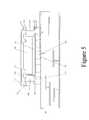
- FIG. 5illustrates a view of the semiconductor device package on board level temperature cycling test according to the present invention.
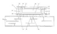
- the present inventiondiscloses a structure of fan-out WLP utilizing a substrate having predetermined terminal contact metal pads 104 formed thereon and a pre-formed through hole 106 formed into the substrate 102 .
- a dieis disposed within the die receiving through hole of the substrate and attached on core paste material, for example, an elastic core paste material is filled into the space between die edge and side wall of die receiving through hole of the substrate or under the die.
- a photosensitive materialis coated over the die and the pre-formed substrate (includes the core paste area), and forming the photosensitive material at lower surface thereof.
- the material of the photosensitive materialis formed of elastic material.
- FIG. 1illustrates a cross-sectional view of Fan-Out Wafer Level Package (FO-WLP) in accordance with one embodiment of the present invention.
- the structure of FO-WLPincludes a substrate 102 having a first terminal contact conductive pads 104 (for organic substrate) and die receiving through holes 106 formed therein to receive a die 108 .
- the die receiving through holes 106is formed from the upper surface of the substrate through the substrate to the lower surface.
- the through hole 106is pre-formed within the substrate 102 .
- the core paste material 110is printed/coated/dispensing under the lower surface of the die 108 , thereby sealing the die 108 .
- the core paste 110is also refilled within the space (gap) between the die edge 108 and the sidewalls of the through holes 108 .
- a conductive (metal) layer 112is coated on the sidewall of the die receiving through holes 106 as optional process to improve the adhesion between core paste and substrate.
- the die 108is disposed within the die receiving through holes 106 on the core paste material 110 .
- contact pads (Bonding pads) 114are formed on the die 108 in active surface site.
- a photosensitive layer or dielectric layer 116is formed over the die 108 and the upper surface of substrate 102 .
- Pluralities of openingsare formed within the dielectric layer 116 through the lithography process or exposure and develop procedure. The pluralities of openings are aligned to the contact pads (or I/O pads) 114 and the first terminal contact conductive pads 104 on the upper surface of the substrate 102 , respectively.
- the RDL (redistribution layer) 118is formed on the dielectric layer 116 by removing selected portions of metal layer formed over the layer 116 , wherein the RDL 118 keeps electrically connected with the die 108 through the I/O pads 114 and the first terminal contact conductive pads 104 .
- a protection layer 126is employed to cover the RDL 118 .
- the substrate 102further comprises connecting through holes 120 formed within the substrate 102 .
- the first terminal contact metal pads 104are formed over the connecting through holes 120 .
- the conductive materialis re-filled into the connecting through holes 120 for electrical connection.
- a scribe line 124is defined between the package units for separating each unit, optionally, there is no dielectric layer over the scribe line.
- Second terminal contact conductive pads 122are located at the lower surface of the substrate 102 and under the connecting through holes 120 and connected to the first terminal contact conductive pads 104 of the substrate 102 .
- a photosensitive layer or dielectric layer 128is formed over the second terminal contact conductive pads 122 , and at the lower surface of the core paste material 110 and substrate 102 . It may be sued the laser to open the core paste materials 110 under the die (die back site) if it is need to connect the back site of said die for grounding or heat dissipation. Pluralities of openings are formed within the dielectric layer 128 through the lithography process or exposure and develop procedure.
- the pluralities of openingsare aligned to the second terminal contact conductive pads 122 on the upper surface of the substrate 102 to form contact via, respectively.
- the RDL (conductive trace) 130is formed on the dielectric layer 128 by removing selected portions of metal layer formed over the layer 128 .
- a protection layer 132is formed to cover the RDL 130 , and pluralities of openings are formed on protection layer 132 to form UBM (Under Ball Metal) 134 .
- Conductive balls 136are formed on the UBM 134 .
- the dielectric layers 116 and 126 , and the core paste material 110act as buffer area that absorbs the thermal mechanical stress between the die 108 and substrate 102 during temperature cycling due to the dielectric layers have elastic property. Additionally, the dielectric layers 128 and 132 further aid in absorbing the thermal mechanical stress.
- the aforementioned structureconstructs a BGA type package.
- the material of the substrate 102is organic substrate likes epoxy type FR5, BT, PCB with defined through holes or Cu metal with pre-etching circuit.
- the CTEis the same as the one of the mother board (PCB).
- the organic substrate with high Glass transition temperature (Tg)are epoxy type FR5 or BT (Bismaleimide triazine) type substrate.
- the Cu metal (CTE around 16)can be used also.
- the glass, ceramic, siliconcan be used as the substrate.
- the elastic core pasteis formed of silicone rubber elastic materials.
- the CTE (X/Y direction) of the epoxy type organic substrate (FR5/BT)is around 16 and the CTE in Z direction is about 60, and the CTE of the tool for chip redistribution can be selected to close the CTE of substrate, then, it can reduce the die shift issue during the temperature curing of core paste materials.
- the FR5/BTis unlikely to return to original location after the temperature cycling (the temperature is close to Glass transition temperature Tg) if using the materials with CTE mismatching that causes the die shift in panel form during the WLP process which needs several high temperature process, for instant, the curing temperature of dielectric layers and core paste curing etc.
- the substratecould be round type such as wafer type, the diameter could be 200, 300 mm or higher. It could be employed for rectangular type such as panel form.
- the substrate 102is pre-formed with die receiving through holes 106 .
- the scribe line 124is defined between the units for separating each unit. Please refer to FIG. 2 , it shows that the substrate 102 includes a plurality of pre-formed die receiving through hole 106 and the connecting through holes 120 . Conductive material is re-filled into the connecting through holes 120 , thereby constructing the connecting through-hole structures.
- the dielectric layers 116 , 128 or 132are preferably an elastic dielectric material which is made by silicone dielectric based materials comprising siloxane polymers (SINR), Dow Corning WL5000 series, and the combination thereof.
- the dielectric layersare made by a material comprising, polyimides (PI) or silicone resin. Preferably, they are photosensitive layers for simple process.
- the elastic dielectric layeris a kind of material with CTE larger than 100 (ppm/° C.), elongation rate about 40 percent (preferably 30 percent-50 percent), and the hardness of the material is between plastic and rubber.
- the thickness of the elastic dielectric layersdepend on the stress accumulated in the RDL/dielectric layer interface during temperature cycling test.
- FIG. 3illustrates the tool 300 for BT/FR5 carrier (it maybe Glass, Silicon, Ceramic or metal/Alloy) and the substrate 102 .
- Adhesion materials 302such as UV curing type material are formed at the periphery area of the tool 300 .
- the toolcould be made of BT/FR5 with the shape of panel form.
- the connecting through holes structureswill not be formed at the edge of the substrate.
- the lower portion of FIG. 3illustrates the combination of the tool 300 and the substrate 102 .
- the panelwill be adhesion with the BT/FR5 carrier, it will stick and hold the panel during process.
- the thickness of carriercould be around 400 um to 600 um.
- FIG. 4illustrates the top view of the substrate 102 having die receiving through holes 106 .
- the edge area 400 of substrate 102does not have the die receiving through holes 106 , it is employed for sticking the BT/FR5 carrier during WLP process. After the WLP process is completed, the substrate 102 will be cut along the dot line from the glass carrier, or cutting the adhesion materials to separate the panel and carrier, it means that the inside area of dot line will be processed by the sawing process for package singulation.
- FIG. 5it illustrates the major portions that associate with the CTE issue.
- the silicon die 108(CTE is ⁇ 2.3) is packaged inside the package.
- FR5 or BT organic epoxy type material(CTE ⁇ 16) is employed as the substrate 102 and its CTE is the same as the PCB or Mother Board 502 .
- the space (gap) between the die 108 and the substrate 102is filled with filling material (prefer the elastic core paste) to absorb the thermal mechanical stress due to CTE mismatching (between die and the epoxy type FR5/BT).
- the dielectric layers 116include elastic materials to absorb the stress between the die I/O pads and the PCB 502 .
- the RDL metalis Cu/Au materials and the CTE is around 16 which is the same as the PCB 502 and organic substrate, and the UBM 134 of contact bumps 136 is located under the terminal contact metal pads 104 of substrate 102 (some of them).
- the metal land of PCB 502is Cu composition metal, the CTE of Cu is around 16 that is match to the one of PCB. From the description above, the present invention may provide excellent CTE (fully matching in X/Y direction) solution for the FO-WLP.
- CTE matching issue under the build up layers (PCB and substrate)is solved by the present scheme and it provides better reliability (no thermal stress in X/Y directions for terminal pads (solder balls/bumps) on the substrate during on board level condition) and the elastic dielectric layers are employed to absorb the Z direction stress.
- the space (gap) between chip 108 edge and sidewall of through holes 120 of substrate 102can be used to fill the elastic dielectric materials to absorb the mechanical/thermal stress.
- the material of the RDLcomprises Ti/Cu/Au alloy or Ti/Cu/Ni/Au alloy; the thickness of the RDL is the range of 2 um and 15 um.
- the Ti/Cu alloyis formed by sputtering technique also as seed metal layers, and the Cu/Au or Cu/Ni/Au alloy is formed by electroplating; exploiting the electro-plating process to form the RDL can make the RDL thick enough and better mechanical properties to withstand CTE mismatching during temperature cycling.
- the metal padscan be Al or Cu or combination thereof. If the structure of FO-WLP utilizes SINR as the elastic dielectric layer and Cu as the RDL, according the stress analysis not shown here, the stress accumulated in the RDL/dielectric layer interface is reduced.
- the RDLsfan out from the die 108 and they communicate toward the second terminal pads 122 and UBM 134 downwardly.
- the die 108is received within the pre-formed die receiving through hole 106 of the substrate 102 , thereby reducing the thickness of the package.
- the prior artviolates the rule to reduce the die package thickness.
- the package of the present inventionwill be thinner than the prior art.
- the substrateis pre-prepared before package.
- the through hole 106is pre-determined. Thus, the throughput will be improved than ever.
- the present inventiondiscloses a fan-out WLP with reduced thickness and good CTE matching performance.
- the present inventionincludes preparing a substrate (preferably organic substrate FR4/FR5/BT) and contact metal pads are formed on top and bottom surface through the connecting through hole.
- the die receiving through holeis formed with the size larger than die size plus >around 100 um/side.
- the depthis the same (or about 25 um thick than) with the thickness of dice thickness.
- the next stepis lapping the wafer by back-lapping to desired thickness.
- the waferis introduced to dicing procedure to separate the dice.
- process for the present inventionincludes providing a die redistribution (alignment) tool with alignment pattern formed thereon. Then, the patterned glues is printed on the tool (be used for sticking the surface of dice), followed by using pick and place fine alignment system with flip chip function to redistribute the desired dies on the tool with desired pitch. The patterned glues will stick the chips (active surface side) on the tool. Subsequently, the substrate (with die receiving through holes) is bound on the tool and followed by printing elastic core paste material on the space (gap) between die and side walls of through holes of the (FR5/BT) substrate and the die back side. It is preferred to keep the surface of the core paste and the substrate at the same level.
- the curing processis used to cure the core paste material and bonding the carrier by UV or thermal curing.
- the panel bonderis used to bond the carrier on to the substrate and die back side. Vacuum bonding is performed, followed by separating the tool from the panel wafer.
- a clean up procedureis performed to clean the dice surface by wet and/or dry clean.
- Next stepis to coat the dielectric materials on the surface of panel. Subsequently, lithography process is performed to open via (contact metal pads) and Al bonding pads or the scribe line (optional). Plasma clean step is then executed to clean the surface of via holes and Al bonding pads.
- Next stepis to sputter Ti/Cu as seed metal layers, and then Photo Resistor (PR) is coated over the dielectric layer and seed metal layers for forming the patterns of redistributed metal layers (RDL).
- PRPhoto Resistor
- the electro platingis processed to form Cu/Au or Cu/Ni/Au as the RDL metal, followed by stripping the PR and metal wet etching to form the RDL metal trace.
- the next stepis to coat or print the top dielectric layer and to open the contact metal via (optional for final testing) or to open the scribe line (optional). It can repeat the procedures to form multi-RDL layers and dielectric layer, such as seed layer, PR, E-plating or strip/etching.
- a clean up procedureis performed to clean the back side of the panel by wet and/or dry clean, optionally, to laser open the back site of die (if it is needed).
- Next stepis to coat the dielectric materials on the back surface of panel to form the dielectric layer. Subsequently, lithography process is performed to open via (contact metal pads) and/or the partial of back site of die.
- Next stepis to sputter Ti/Cu as seed metal layers on the dielectric layer, and then Photo Resistor (PR) is coated over the dielectric layer and seed metal layers for forming the patterns of redistributed metal layers (RDL).
- PRPhoto Resistor
- the electro platingis processed to form Cu/Au or Cu/Ni/Au as the RDL metal, followed by stripping the PR and metal wet etching to form the RDL metal trace. Subsequently, the next step is to coat or print the top dielectric layer and to open the contact metal pads to form UBM.
- the heat re-flow procedureis performed to re-flow on the ball side (for BGA type).
- the testingis executed.
- Panel wafer level final testingis performed by using vertical or epoxy probe card to contact the solder balls or bumps. After the testing, the substrate is sawed to singular the package into individual units. Then, the packages are respectively picked and placed the package on the tray or tape and reel.
- the processis simple for forming Panel wafer type and is easy to control the roughness of panel surface.
- the thickness of panelis easy to be controlled and die shift issue will be eliminated during process.
- the injection mold toolis omitted, CMP polish process will not be introduced either, and no warp result from the process.
- the panel waferis easy to be processed by wafer level packaging process.
- CTE match under the build up layers (PCB and substrate)has better reliability that no thermal stress results in X/Y direction on board and by using elastic dielectric layers to absorb the stress from Z direction. Single material is sawed during singulation.
- the substrateis pre-prepared with pre-form through holes, inter-connecting through holes and terminal contact metal pads (for organic substrate); the size of die receiving through hole is equal to die size plus around >100 um per/side; it can be used as stress buffer releasing area by filling the elastic core paste materials to absorb the thermal stress due to the CTE between silicon die and substrate (FR5/BT)) is difference, additionally, it can fill the elastic dielectric materials to the gap between die edge and side wall of the substrate to absorb the mechanical or thermal stress due to the CTE mismatch.
- the packaging throughputwill be increased (manufacturing cycle time was reduced) due to apply the simple build up layers on top the surface of die and bottom site.
- the terminal padsare formed on the opposite side of the dice active surface.
- the dice placement processis the same as the current process.
- Elastic core pasteresin, epoxy compound, silicone rubber, etc.
- CTE mismatching issueis overcome during panel form process (using the BT/FR5 carrier with same CTE of substrate).
- the deepness between the die and substrateis about 25 um, and the dielectric layer and RDL are formed on both the upper and lower surface of the panel. Only silicone dielectric material (preferably SINR) is coated on the active surface and the substrate (preferably FR45 or BT) surface.
- the contact padsare opened by using photo mask process only due to the dielectric layer (SINR) is photosensitive layer for opening the contacting open.
- the die and substratebe bonded together with carrier.
- the reliability for both package and board levelis better than ever, especially, for the board level temperature cycling test, it was due to the CTE of substrate and PCB mother board are identical, hence, no thermal mechanical stress be applied on the solder bumps/balls; and thickness of the package with protection is extremely thin which is less 200 um.
- the costis low and the process is simple. It is easy to form the multi-chips package as well.
Landscapes
- Engineering & Computer Science (AREA)
- Computer Hardware Design (AREA)
- Microelectronics & Electronic Packaging (AREA)
- Power Engineering (AREA)
- Physics & Mathematics (AREA)
- Condensed Matter Physics & Semiconductors (AREA)
- General Physics & Mathematics (AREA)
- Production Of Multi-Layered Print Wiring Board (AREA)
- Structures Or Materials For Encapsulating Or Coating Semiconductor Devices Or Solid State Devices (AREA)
- Internal Circuitry In Semiconductor Integrated Circuit Devices (AREA)
Abstract
Description
Claims (12)
Priority Applications (11)
| Application Number | Priority Date | Filing Date | Title |
|---|---|---|---|
| US11/694,719US8178964B2 (en) | 2007-03-30 | 2007-03-30 | Semiconductor device package with die receiving through-hole and dual build-up layers over both side-surfaces for WLP and method of the same |
| US11/933,703US20080157327A1 (en) | 2007-01-03 | 2007-11-01 | Package on package structure for semiconductor devices and method of the same |
| US11/936,596US20080237828A1 (en) | 2007-03-30 | 2007-11-07 | Semiconductor device package with die receiving through-hole and dual build-up layers over both side-surfaces for wlp and method of the same |
| US11/954,087US7423335B2 (en) | 2006-12-29 | 2007-12-11 | Sensor module package structure and method of the same |
| TW097102714ATWI360208B (en) | 2007-03-30 | 2008-01-24 | Semiconductor device package with die receiving th |
| TW097111497ATWI352413B (en) | 2007-03-30 | 2008-03-28 | Semiconductor device package with die receiving th |
| DE102008016324ADE102008016324A1 (en) | 2007-03-30 | 2008-03-28 | Semiconductor device package with a chip-receiving through hole and double-sided build-up layers on both surfaces sides for WLP and a method to do so |
| SG200802522-3ASG146596A1 (en) | 2007-03-30 | 2008-03-31 | Semiconductor device package with die receiving through-hole and dual side build-up layers over both side-surfaces for wlp and method of the same |
| JP2008090882AJP2008258621A (en) | 2007-03-30 | 2008-03-31 | Semiconductor device package structure and method for forming semiconductor device package structure |
| KR1020080029831AKR20080089311A (en) | 2007-03-30 | 2008-03-31 | Semiconductor device package and method having die receiving through holes for JP and double side build up layers on both surfaces |
| CNA2008100894210ACN101325188A (en) | 2007-03-30 | 2008-03-31 | Wafer level semiconductor package with double-sided build-up and method thereof |
Applications Claiming Priority (1)
| Application Number | Priority Date | Filing Date | Title |
|---|---|---|---|
| US11/694,719US8178964B2 (en) | 2007-03-30 | 2007-03-30 | Semiconductor device package with die receiving through-hole and dual build-up layers over both side-surfaces for WLP and method of the same |
Related Child Applications (2)
| Application Number | Title | Priority Date | Filing Date |
|---|---|---|---|
| US11/648,688Continuation-In-PartUS8178963B2 (en) | 2006-12-29 | 2007-01-03 | Wafer level package with die receiving through-hole and method of the same |
| US11/936,596Continuation-In-PartUS20080237828A1 (en) | 2007-03-30 | 2007-11-07 | Semiconductor device package with die receiving through-hole and dual build-up layers over both side-surfaces for wlp and method of the same |
Publications (2)
| Publication Number | Publication Date |
|---|---|
| US20080237879A1 US20080237879A1 (en) | 2008-10-02 |
| US8178964B2true US8178964B2 (en) | 2012-05-15 |
Family
ID=39792849
Family Applications (1)
| Application Number | Title | Priority Date | Filing Date |
|---|---|---|---|
| US11/694,719Active2029-04-07US8178964B2 (en) | 2006-12-29 | 2007-03-30 | Semiconductor device package with die receiving through-hole and dual build-up layers over both side-surfaces for WLP and method of the same |
Country Status (3)
| Country | Link |
|---|---|
| US (1) | US8178964B2 (en) |
| CN (1) | CN101325188A (en) |
| TW (1) | TWI360208B (en) |
Cited By (25)
| Publication number | Priority date | Publication date | Assignee | Title |
|---|---|---|---|---|
| US9093439B2 (en) | 2012-09-12 | 2015-07-28 | Samsung Electronics Co., Ltd. | Semiconductor package and method of fabricating the same |
| US9721933B2 (en) | 2014-02-27 | 2017-08-01 | Taiwan Semiconductor Manufacturing Company, Ltd. | Laser marking in packages |
| US9780014B1 (en) | 2011-11-29 | 2017-10-03 | Hrl Laboratories, Llc | Simultaneous controlled depth hot embossing and active side protection during packaging and assembly of wide bandgap devices |
| US9837372B1 (en) | 2015-05-22 | 2017-12-05 | Hrl Laboratories, Llc | Wafer-level die to package and die to die interconnects suspended over integrated heat sinks |
| US20180076147A1 (en)* | 2016-09-12 | 2018-03-15 | Samsung Electro-Mechanics Co., Ltd. | Semiconductor package, method of manufacturing the same, and electronic device module |
| US10026672B1 (en) | 2015-10-21 | 2018-07-17 | Hrl Laboratories, Llc | Recursive metal embedded chip assembly |
| US10079160B1 (en)* | 2013-06-21 | 2018-09-18 | Hrl Laboratories, Llc | Surface mount package for semiconductor devices with embedded heat spreaders |
| US10269723B2 (en) | 2014-05-29 | 2019-04-23 | Taiwan Semiconductor Manufacturing Company, Ltd. | Alignment mark design for packages |
| US10879226B2 (en) | 2016-05-19 | 2020-12-29 | Invensas Bonding Technologies, Inc. | Stacked dies and methods for forming bonded structures |
| US10950562B1 (en) | 2018-11-30 | 2021-03-16 | Hrl Laboratories, Llc | Impedance-matched through-wafer transition using integrated heat-spreader technology |
| US11056390B2 (en) | 2015-06-24 | 2021-07-06 | Invensas Corporation | Structures and methods for reliable packages |
| US11387214B2 (en) | 2017-06-15 | 2022-07-12 | Invensas Llc | Multi-chip modules formed using wafer-level processing of a reconstituted wafer |
| US11462419B2 (en) | 2018-07-06 | 2022-10-04 | Invensas Bonding Technologies, Inc. | Microelectronic assemblies |
| US11476213B2 (en) | 2019-01-14 | 2022-10-18 | Invensas Bonding Technologies, Inc. | Bonded structures without intervening adhesive |
| US11538781B2 (en) | 2020-06-30 | 2022-12-27 | Adeia Semiconductor Bonding Technologies Inc. | Integrated device packages including bonded structures |
| US11594509B2 (en) | 2016-10-06 | 2023-02-28 | Compass Technology Company Limited | Fabrication process and structure of fine pitch traces for a solid state diffusion bond on flip chip interconnect |
| US11652083B2 (en) | 2017-05-11 | 2023-05-16 | Adeia Semiconductor Bonding Technologies Inc. | Processed stacked dies |
| US11728273B2 (en) | 2020-09-04 | 2023-08-15 | Adeia Semiconductor Bonding Technologies Inc. | Bonded structure with interconnect structure |
| US11749595B2 (en) | 2016-10-06 | 2023-09-05 | Compass Technology Company Limited | Fabrication process and structure of fine pitch traces for a solid state diffusion bond on flip chip interconnect |
| US11764177B2 (en) | 2020-09-04 | 2023-09-19 | Adeia Semiconductor Bonding Technologies Inc. | Bonded structure with interconnect structure |
| US11764189B2 (en) | 2018-07-06 | 2023-09-19 | Adeia Semiconductor Bonding Technologies Inc. | Molded direct bonded and interconnected stack |
| US11916054B2 (en) | 2018-05-15 | 2024-02-27 | Adeia Semiconductor Bonding Technologies Inc. | Stacked devices and methods of fabrication |
| US11935907B2 (en) | 2014-12-11 | 2024-03-19 | Adeia Semiconductor Technologies Llc | Image sensor device |
| US11955463B2 (en) | 2019-06-26 | 2024-04-09 | Adeia Semiconductor Bonding Technologies Inc. | Direct bonded stack structures for increased reliability and improved yield in microelectronics |
| US12080672B2 (en) | 2019-09-26 | 2024-09-03 | Adeia Semiconductor Bonding Technologies Inc. | Direct gang bonding methods including directly bonding first element to second element to form bonded structure without adhesive |
Families Citing this family (40)
| Publication number | Priority date | Publication date | Assignee | Title |
|---|---|---|---|---|
| US9000461B2 (en)* | 2003-07-04 | 2015-04-07 | Epistar Corporation | Optoelectronic element and manufacturing method thereof |
| TWI360207B (en) | 2007-10-22 | 2012-03-11 | Advanced Semiconductor Eng | Chip package structure and method of manufacturing |
| TWI453877B (en)* | 2008-11-07 | 2014-09-21 | Advanced Semiconductor Eng | Structure and process of embedded chip package |
| US8237257B2 (en)* | 2008-09-25 | 2012-08-07 | King Dragon International Inc. | Substrate structure with die embedded inside and dual build-up layers over both side surfaces and method of the same |
| US8350377B2 (en)* | 2008-09-25 | 2013-01-08 | Wen-Kun Yang | Semiconductor device package structure and method for the same |
| US8106504B2 (en)* | 2008-09-25 | 2012-01-31 | King Dragon International Inc. | Stacking package structure with chip embedded inside and die having through silicon via and method of the same |
| WO2010106473A1 (en)* | 2009-03-16 | 2010-09-23 | Nxp B.V. | Packaged semiconductor product and method for manufacture thereof |
| US8531015B2 (en)* | 2009-03-26 | 2013-09-10 | Stats Chippac, Ltd. | Semiconductor device and method of forming a thin wafer without a carrier |
| TWI456715B (en)* | 2009-06-19 | 2014-10-11 | Advanced Semiconductor Eng | Chip package structure and manufacturing method thereof |
| TWI474447B (en)* | 2009-06-29 | 2015-02-21 | Advanced Semiconductor Eng | Semiconductor package structure and enveloping method thereof |
| US8569894B2 (en) | 2010-01-13 | 2013-10-29 | Advanced Semiconductor Engineering, Inc. | Semiconductor package with single sided substrate design and manufacturing methods thereof |
| US8320134B2 (en) | 2010-02-05 | 2012-11-27 | Advanced Semiconductor Engineering, Inc. | Embedded component substrate and manufacturing methods thereof |
| TWI411075B (en) | 2010-03-22 | 2013-10-01 | Advanced Semiconductor Eng | Semiconductor package and manufacturing method thereof |
| TWI426587B (en)* | 2010-08-12 | 2014-02-11 | 矽品精密工業股份有限公司 | Chip scale package and fabrication method thereof |
| US20120037935A1 (en)* | 2010-08-13 | 2012-02-16 | Wen-Kun Yang | Substrate Structure of LED (light emitting diode) Packaging and Method of the same |
| TWI533412B (en)* | 2010-08-13 | 2016-05-11 | 金龍國際公司 | Semiconductor device package structure and forming method of the same |
| US8941222B2 (en) | 2010-11-11 | 2015-01-27 | Advanced Semiconductor Engineering Inc. | Wafer level semiconductor package and manufacturing methods thereof |
| US9406658B2 (en) | 2010-12-17 | 2016-08-02 | Advanced Semiconductor Engineering, Inc. | Embedded component device and manufacturing methods thereof |
| US8487426B2 (en) | 2011-03-15 | 2013-07-16 | Advanced Semiconductor Engineering, Inc. | Semiconductor package with embedded die and manufacturing methods thereof |
| TWM421298U (en) | 2011-09-20 | 2012-01-21 | xue-li Dai | Bottle cap safety ring structure having carrying function |
| TWI466282B (en)* | 2011-11-23 | 2014-12-21 | Tong Hsing Electronic Ind Ltd | Image sensing module package structure and manufacturing method |
| US20130186676A1 (en) | 2012-01-20 | 2013-07-25 | Futurewei Technologies, Inc. | Methods and Apparatus for a Substrate Core Layer |
| US8809996B2 (en)* | 2012-06-29 | 2014-08-19 | Taiwan Semiconductor Manufacturing Company, Ltd. | Package with passive devices and method of forming the same |
| CN104124221B (en)* | 2013-04-23 | 2016-12-28 | 万国半导体(开曼)股份有限公司 | Slim power device and preparation method thereof |
| CN104576575B (en)* | 2013-10-10 | 2017-12-19 | 日月光半导体制造股份有限公司 | Semiconductor package and manufacturing method thereof |
| CN105280575A (en)* | 2014-07-17 | 2016-01-27 | 联华电子股份有限公司 | Semiconductor package structure and manufacturing method thereof |
| KR101634067B1 (en)* | 2014-10-01 | 2016-06-30 | 주식회사 네패스 | Semiconductor package and method of manufacturing the same |
| US9536753B2 (en)* | 2014-10-02 | 2017-01-03 | Texas Instruments Incorporated | Circuit substrate interconnect |
| CN104600185B (en)* | 2014-12-31 | 2017-10-27 | 江阴长电先进封装有限公司 | A kind of LED encapsulation structure and its wafer-level packaging method |
| US9508664B1 (en) | 2015-12-16 | 2016-11-29 | Taiwan Semiconductor Manufacturing Company, Ltd. | Semiconductor device structure comprising a plurality of metal oxide fibers and method for forming the same |
| US10103095B2 (en)* | 2016-10-06 | 2018-10-16 | Compass Technology Company Limited | Fabrication process and structure of fine pitch traces for a solid state diffusion bond on flip chip interconnect |
| US10541218B2 (en)* | 2016-11-29 | 2020-01-21 | Taiwan Semiconductor Manufacturing Company, Ltd. | Redistribution layer structure and fabrication method therefor |
| CN112352305B (en)* | 2018-06-26 | 2023-03-03 | 华为技术有限公司 | Chip packaging structure and chip packaging method |
| KR102589683B1 (en)* | 2018-11-16 | 2023-10-16 | 삼성전자주식회사 | Fan-out semiconductor package |
| CN109920763A (en)* | 2019-03-04 | 2019-06-21 | 积高电子(无锡)有限公司 | A kind of surface mount semiconductor resistance bridge package substrate and packaging technology |
| JP2020184589A (en)* | 2019-05-09 | 2020-11-12 | イビデン株式会社 | Electronic component built-in wiring board and method for manufacturing the same |
| CN112908943A (en)* | 2021-01-12 | 2021-06-04 | 华为技术有限公司 | Embedded packaging structure, preparation method thereof and terminal equipment |
| TWI765652B (en)* | 2021-04-09 | 2022-05-21 | 晶英科技股份有限公司 | Electrical inspection device formed on wafer substrate using semiconductor process |
| CN115201537A (en)* | 2021-04-12 | 2022-10-18 | 晶英科技股份有限公司 | Electrical inspection device formed on wafer substrate using semiconductor process |
| US20240063083A1 (en)* | 2022-08-19 | 2024-02-22 | Taiwan Semiconductor Manufacturing Co., Ltd. | Redistribution Structure with Warpage Tuning Layer |
Citations (3)
| Publication number | Priority date | Publication date | Assignee | Title |
|---|---|---|---|---|
| US6127634A (en)* | 1994-10-11 | 2000-10-03 | Fujitsu Limited | Wiring board with an insulating layer to prevent gap formation during etching |
| US20040106229A1 (en)* | 2002-06-27 | 2004-06-03 | Tongbi Jiang | Methods for assembling multiple semiconductor devices |
| US6952049B1 (en)* | 1999-03-30 | 2005-10-04 | Ngk Spark Plug Co., Ltd. | Capacitor-built-in type printed wiring substrate, printed wiring substrate, and capacitor |
- 2007
- 2007-03-30USUS11/694,719patent/US8178964B2/enactiveActive
- 2008
- 2008-01-24TWTW097102714Apatent/TWI360208B/enactive
- 2008-03-31CNCNA2008100894210Apatent/CN101325188A/ennot_activeWithdrawn
Patent Citations (3)
| Publication number | Priority date | Publication date | Assignee | Title |
|---|---|---|---|---|
| US6127634A (en)* | 1994-10-11 | 2000-10-03 | Fujitsu Limited | Wiring board with an insulating layer to prevent gap formation during etching |
| US6952049B1 (en)* | 1999-03-30 | 2005-10-04 | Ngk Spark Plug Co., Ltd. | Capacitor-built-in type printed wiring substrate, printed wiring substrate, and capacitor |
| US20040106229A1 (en)* | 2002-06-27 | 2004-06-03 | Tongbi Jiang | Methods for assembling multiple semiconductor devices |
Cited By (48)
| Publication number | Priority date | Publication date | Assignee | Title |
|---|---|---|---|---|
| US9780014B1 (en) | 2011-11-29 | 2017-10-03 | Hrl Laboratories, Llc | Simultaneous controlled depth hot embossing and active side protection during packaging and assembly of wide bandgap devices |
| US9093439B2 (en) | 2012-09-12 | 2015-07-28 | Samsung Electronics Co., Ltd. | Semiconductor package and method of fabricating the same |
| US10079160B1 (en)* | 2013-06-21 | 2018-09-18 | Hrl Laboratories, Llc | Surface mount package for semiconductor devices with embedded heat spreaders |
| US9721933B2 (en) | 2014-02-27 | 2017-08-01 | Taiwan Semiconductor Manufacturing Company, Ltd. | Laser marking in packages |
| US11742298B2 (en) | 2014-05-29 | 2023-08-29 | Taiwan Semiconductor Manufacturing Company, Ltd. | Alignment mark design for packages |
| US10522473B2 (en) | 2014-05-29 | 2019-12-31 | Taiwan Semiconductor Manufacturing Company, Ltd. | Alignment mark design for packages |
| US10269723B2 (en) | 2014-05-29 | 2019-04-23 | Taiwan Semiconductor Manufacturing Company, Ltd. | Alignment mark design for packages |
| US11935907B2 (en) | 2014-12-11 | 2024-03-19 | Adeia Semiconductor Technologies Llc | Image sensor device |
| US12324268B2 (en) | 2014-12-11 | 2025-06-03 | Adeia Semiconductor Technologies Llc | Image sensor device |
| US9837372B1 (en) | 2015-05-22 | 2017-12-05 | Hrl Laboratories, Llc | Wafer-level die to package and die to die interconnects suspended over integrated heat sinks |
| US11056390B2 (en) | 2015-06-24 | 2021-07-06 | Invensas Corporation | Structures and methods for reliable packages |
| US10483184B1 (en) | 2015-10-21 | 2019-11-19 | Hrl Laboratories, Llc | Recursive metal embedded chip assembly |
| US10026672B1 (en) | 2015-10-21 | 2018-07-17 | Hrl Laboratories, Llc | Recursive metal embedded chip assembly |
| US10879226B2 (en) | 2016-05-19 | 2020-12-29 | Invensas Bonding Technologies, Inc. | Stacked dies and methods for forming bonded structures |
| US12113056B2 (en) | 2016-05-19 | 2024-10-08 | Adeia Semiconductor Bonding Technologies Inc. | Stacked dies and methods for forming bonded structures |
| US11658173B2 (en) | 2016-05-19 | 2023-05-23 | Adeia Semiconductor Bonding Technologies Inc. | Stacked dies and methods for forming bonded structures |
| US11837596B2 (en) | 2016-05-19 | 2023-12-05 | Adeia Semiconductor Bonding Technologies Inc. | Stacked dies and methods for forming bonded structures |
| US12266650B2 (en) | 2016-05-19 | 2025-04-01 | Adeia Semiconductor Bonding Technologies Inc. | Stacked dies and methods for forming bonded structures |
| US10068855B2 (en)* | 2016-09-12 | 2018-09-04 | Samsung Electro-Mechanics Co., Ltd. | Semiconductor package, method of manufacturing the same, and electronic device module |
| US20180076147A1 (en)* | 2016-09-12 | 2018-03-15 | Samsung Electro-Mechanics Co., Ltd. | Semiconductor package, method of manufacturing the same, and electronic device module |
| US11749595B2 (en) | 2016-10-06 | 2023-09-05 | Compass Technology Company Limited | Fabrication process and structure of fine pitch traces for a solid state diffusion bond on flip chip interconnect |
| US11594509B2 (en) | 2016-10-06 | 2023-02-28 | Compass Technology Company Limited | Fabrication process and structure of fine pitch traces for a solid state diffusion bond on flip chip interconnect |
| US12068278B2 (en) | 2017-05-11 | 2024-08-20 | Adeia Semiconductor Bonding Technologies Inc. | Processed stacked dies |
| US11652083B2 (en) | 2017-05-11 | 2023-05-16 | Adeia Semiconductor Bonding Technologies Inc. | Processed stacked dies |
| US12374656B2 (en) | 2017-06-15 | 2025-07-29 | Adeia Semiconductor Bonding Technologies Inc. | Multi-chip modules formed using wafer-level processing of a reconstituted wafer |
| US11387214B2 (en) | 2017-06-15 | 2022-07-12 | Invensas Llc | Multi-chip modules formed using wafer-level processing of a reconstituted wafer |
| US12347820B2 (en) | 2018-05-15 | 2025-07-01 | Adeia Semiconductor Bonding Technologies Inc. | Stacked devices and methods of fabrication |
| US12401011B2 (en) | 2018-05-15 | 2025-08-26 | Adeia Semiconductor Bonding Technologies Inc. | Stacked devices and methods of fabrication |
| US11916054B2 (en) | 2018-05-15 | 2024-02-27 | Adeia Semiconductor Bonding Technologies Inc. | Stacked devices and methods of fabrication |
| US11764189B2 (en) | 2018-07-06 | 2023-09-19 | Adeia Semiconductor Bonding Technologies Inc. | Molded direct bonded and interconnected stack |
| US12341025B2 (en) | 2018-07-06 | 2025-06-24 | Adeia Semiconductor Bonding Technologies Inc. | Microelectronic assemblies |
| US11837582B2 (en) | 2018-07-06 | 2023-12-05 | Adeia Semiconductor Bonding Technologies Inc. | Molded direct bonded and interconnected stack |
| US11462419B2 (en) | 2018-07-06 | 2022-10-04 | Invensas Bonding Technologies, Inc. | Microelectronic assemblies |
| US12266640B2 (en) | 2018-07-06 | 2025-04-01 | Adeia Semiconductor Bonding Technologies Inc. | Molded direct bonded and interconnected stack |
| US12046482B2 (en) | 2018-07-06 | 2024-07-23 | Adeia Semiconductor Bonding Technologies, Inc. | Microelectronic assemblies |
| US10950562B1 (en) | 2018-11-30 | 2021-03-16 | Hrl Laboratories, Llc | Impedance-matched through-wafer transition using integrated heat-spreader technology |
| US11817409B2 (en) | 2019-01-14 | 2023-11-14 | Adeia Semiconductor Bonding Technologies Inc. | Directly bonded structures without intervening adhesive and methods for forming the same |
| US11476213B2 (en) | 2019-01-14 | 2022-10-18 | Invensas Bonding Technologies, Inc. | Bonded structures without intervening adhesive |
| US11955463B2 (en) | 2019-06-26 | 2024-04-09 | Adeia Semiconductor Bonding Technologies Inc. | Direct bonded stack structures for increased reliability and improved yield in microelectronics |
| US12272677B2 (en) | 2019-06-26 | 2025-04-08 | Adeia Semiconductor Bonding Technologies Inc. | Direct bonded stack structures for increased reliability and improved yield in microelectronics |
| US12080672B2 (en) | 2019-09-26 | 2024-09-03 | Adeia Semiconductor Bonding Technologies Inc. | Direct gang bonding methods including directly bonding first element to second element to form bonded structure without adhesive |
| US12046569B2 (en) | 2020-06-30 | 2024-07-23 | Adeia Semiconductor Bonding Technologies Inc. | Integrated device packages with integrated device die and dummy element |
| US11631647B2 (en) | 2020-06-30 | 2023-04-18 | Adeia Semiconductor Bonding Technologies Inc. | Integrated device packages with integrated device die and dummy element |
| US11538781B2 (en) | 2020-06-30 | 2022-12-27 | Adeia Semiconductor Bonding Technologies Inc. | Integrated device packages including bonded structures |
| US12176294B2 (en) | 2020-09-04 | 2024-12-24 | Adeia Semiconductor Bonding Technologies, Inc. | Bonded structure with interconnect structure |
| US12322718B2 (en) | 2020-09-04 | 2025-06-03 | Adeia Semiconductor Bonding Technologies Inc. | Bonded structure with interconnect structure |
| US11764177B2 (en) | 2020-09-04 | 2023-09-19 | Adeia Semiconductor Bonding Technologies Inc. | Bonded structure with interconnect structure |
| US11728273B2 (en) | 2020-09-04 | 2023-08-15 | Adeia Semiconductor Bonding Technologies Inc. | Bonded structure with interconnect structure |
Also Published As
| Publication number | Publication date |
|---|---|
| CN101325188A (en) | 2008-12-17 |
| TWI360208B (en) | 2012-03-11 |
| US20080237879A1 (en) | 2008-10-02 |
| TW200839988A (en) | 2008-10-01 |
Similar Documents
| Publication | Publication Date | Title |
|---|---|---|
| US8178964B2 (en) | Semiconductor device package with die receiving through-hole and dual build-up layers over both side-surfaces for WLP and method of the same | |
| US8178963B2 (en) | Wafer level package with die receiving through-hole and method of the same | |
| US7812434B2 (en) | Wafer level package with die receiving through-hole and method of the same | |
| US7459729B2 (en) | Semiconductor image device package with die receiving through-hole and method of the same | |
| US7655501B2 (en) | Wafer level package with good CTE performance | |
| US20080237828A1 (en) | Semiconductor device package with die receiving through-hole and dual build-up layers over both side-surfaces for wlp and method of the same | |
| US20080157358A1 (en) | Wafer level package with die receiving through-hole and method of the same | |
| US8237257B2 (en) | Substrate structure with die embedded inside and dual build-up layers over both side surfaces and method of the same | |
| US8350377B2 (en) | Semiconductor device package structure and method for the same | |
| US7911044B2 (en) | RF module package for releasing stress | |
| US7884461B2 (en) | System-in-package and manufacturing method of the same | |
| US20080116564A1 (en) | Wafer level package with die receiving cavity and method of the same | |
| US20080083980A1 (en) | Cmos image sensor chip scale package with die receiving through-hole and method of the same | |
| US20080217761A1 (en) | Structure of semiconductor device package and method of the same | |
| US20080136002A1 (en) | Multi-chips package and method of forming the same | |
| US20080224306A1 (en) | Multi-chips package and method of forming the same | |
| US20080197469A1 (en) | Multi-chips package with reduced structure and method for forming the same | |
| US7525185B2 (en) | Semiconductor device package having multi-chips with side-by-side configuration and method of the same | |
| US20080157340A1 (en) | RF module package | |
| US20080211075A1 (en) | Image sensor chip scale package having inter-adhesion with gap and method of the same |
Legal Events
| Date | Code | Title | Description |
|---|---|---|---|
| AS | Assignment | Owner name:ADVANCED CHIP ENGINEERING TECHNOLOGY, INC., TAIWAN Free format text:ASSIGNMENT OF ASSIGNORS INTEREST;ASSIGNOR:YANG, WEN-KUN;REEL/FRAME:019925/0285 Effective date:20070328 | |
| STCF | Information on status: patent grant | Free format text:PATENTED CASE | |
| FPAY | Fee payment | Year of fee payment:4 | |
| MAFP | Maintenance fee payment | Free format text:PAYMENT OF MAINTENANCE FEE, 8TH YR, SMALL ENTITY (ORIGINAL EVENT CODE: M2552); ENTITY STATUS OF PATENT OWNER: SMALL ENTITY Year of fee payment:8 | |
| AS | Assignment | Owner name:ADL ENERGY CORP., TAIWAN Free format text:CHANGE OF NAME;ASSIGNOR:ADL ENGINEERING INC.;REEL/FRAME:064927/0462 Effective date:20220105 Owner name:ADL ENGINEERING INC., TAIWAN Free format text:MERGER;ASSIGNORS:ADL ENGINEERING INC.;ADVANCED CHIP ENGINEERING TECHNOLOGY INC.;REEL/FRAME:064926/0845 Effective date:20120613 | |
| MAFP | Maintenance fee payment | Free format text:PAYMENT OF MAINTENANCE FEE, 12TH YR, SMALL ENTITY (ORIGINAL EVENT CODE: M2553); ENTITY STATUS OF PATENT OWNER: SMALL ENTITY Year of fee payment:12 | |
| AS | Assignment | Owner name:TAIWAN SEMICONDUCTOR MANUFACTURING COMPANY, LTD., TAIWAN Free format text:ASSIGNMENT OF ASSIGNORS INTEREST;ASSIGNOR:ADL ENERGY CORP.;REEL/FRAME:065957/0661 Effective date:20230914 |