US8174886B2 - Semiconductor memory having electrically floating body transistor - Google Patents
Semiconductor memory having electrically floating body transistorDownload PDFInfo
- Publication number
- US8174886B2 US8174886B2US13/244,839US201113244839AUS8174886B2US 8174886 B2US8174886 B2US 8174886B2US 201113244839 AUS201113244839 AUS 201113244839AUS 8174886 B2US8174886 B2US 8174886B2
- Authority
- US
- United States
- Prior art keywords
- cell
- terminal
- floating body
- region
- conductivity type
- Prior art date
- Legal status (The legal status is an assumption and is not a legal conclusion. Google has not performed a legal analysis and makes no representation as to the accuracy of the status listed.)
- Active
Links
- 238000007667floatingMethods0.000titleclaimsabstractdescription236
- 239000004065semiconductorSubstances0.000titleclaimsabstractdescription29
- 230000015654memoryEffects0.000claimsabstractdescription389
- 210000000746body regionAnatomy0.000claimsabstractdescription51
- 239000000758substrateSubstances0.000claimsdescription155
- 230000001186cumulative effectEffects0.000claimsdescription15
- 238000012544monitoring processMethods0.000claimsdescription11
- 230000006870functionEffects0.000claimsdescription9
- 230000000737periodic effectEffects0.000claimsdescription6
- 239000011159matrix materialSubstances0.000claimsdescription4
- 238000003491arrayMethods0.000abstractdescription2
- 238000000034methodMethods0.000description28
- 230000007246mechanismEffects0.000description16
- 230000008859changeEffects0.000description15
- 230000005641tunnelingEffects0.000description15
- 238000010586diagramMethods0.000description14
- 239000000463materialSubstances0.000description14
- 230000008569processEffects0.000description14
- 238000002347injectionMethods0.000description9
- 239000007924injectionSubstances0.000description9
- 238000013461designMethods0.000description6
- 229910052710siliconInorganic materials0.000description6
- 239000010703siliconSubstances0.000description6
- XUIMIQQOPSSXEZ-UHFFFAOYSA-NSiliconChemical compound[Si]XUIMIQQOPSSXEZ-UHFFFAOYSA-N0.000description5
- 238000005516engineering processMethods0.000description5
- 238000002513implantationMethods0.000description5
- 230000014759maintenance of locationEffects0.000description5
- JBRZTFJDHDCESZ-UHFFFAOYSA-NAsGaChemical compound[As]#[Ga]JBRZTFJDHDCESZ-UHFFFAOYSA-N0.000description4
- OKTJSMMVPCPJKN-UHFFFAOYSA-NCarbonChemical compound[C]OKTJSMMVPCPJKN-UHFFFAOYSA-N0.000description4
- 229910001218Gallium arsenideInorganic materials0.000description4
- VYPSYNLAJGMNEJ-UHFFFAOYSA-NSilicium dioxideChemical compoundO=[Si]=OVYPSYNLAJGMNEJ-UHFFFAOYSA-N0.000description4
- 229910000577Silicon-germaniumInorganic materials0.000description4
- LEVVHYCKPQWKOP-UHFFFAOYSA-N[Si].[Ge]Chemical compound[Si].[Ge]LEVVHYCKPQWKOP-UHFFFAOYSA-N0.000description4
- 239000003990capacitorSubstances0.000description4
- 239000002041carbon nanotubeSubstances0.000description4
- 229910021393carbon nanotubeInorganic materials0.000description4
- 230000008878couplingEffects0.000description4
- 238000010168coupling processMethods0.000description4
- 238000005859coupling reactionMethods0.000description4
- 239000003989dielectric materialSubstances0.000description4
- 229910052732germaniumInorganic materials0.000description4
- GNPVGFCGXDBREM-UHFFFAOYSA-Ngermanium atomChemical compound[Ge]GNPVGFCGXDBREM-UHFFFAOYSA-N0.000description4
- 230000007935neutral effectEffects0.000description4
- 229910052814silicon oxideInorganic materials0.000description4
- 229910052715tantalumInorganic materials0.000description4
- 238000005468ion implantationMethods0.000description3
- 229910052751metalInorganic materials0.000description3
- 239000002184metalSubstances0.000description3
- GWEVSGVZZGPLCZ-UHFFFAOYSA-NTitan oxideChemical compoundO=[Ti]=OGWEVSGVZZGPLCZ-UHFFFAOYSA-N0.000description2
- RTAQQCXQSZGOHL-UHFFFAOYSA-NTitaniumChemical compound[Ti]RTAQQCXQSZGOHL-UHFFFAOYSA-N0.000description2
- 230000008901benefitEffects0.000description2
- 230000007423decreaseEffects0.000description2
- 238000009792diffusion processMethods0.000description2
- 229910000449hafnium oxideInorganic materials0.000description2
- WIHZLLGSGQNAGK-UHFFFAOYSA-Nhafnium(4+);oxygen(2-)Chemical compound[O-2].[O-2].[Hf+4]WIHZLLGSGQNAGK-UHFFFAOYSA-N0.000description2
- 238000002955isolationMethods0.000description2
- 150000004767nitridesChemical class0.000description2
- TWNQGVIAIRXVLR-UHFFFAOYSA-Noxo(oxoalumanyloxy)alumaneChemical compoundO=[Al]O[Al]=OTWNQGVIAIRXVLR-UHFFFAOYSA-N0.000description2
- RVTZCBVAJQQJTK-UHFFFAOYSA-Noxygen(2-);zirconium(4+)Chemical compound[O-2].[O-2].[Zr+4]RVTZCBVAJQQJTK-UHFFFAOYSA-N0.000description2
- 229910021420polycrystalline siliconInorganic materials0.000description2
- 229920005591polysiliconPolymers0.000description2
- 238000005086pumpingMethods0.000description2
- 239000007787solidSubstances0.000description2
- GUVRBAGPIYLISA-UHFFFAOYSA-Ntantalum atomChemical compound[Ta]GUVRBAGPIYLISA-UHFFFAOYSA-N0.000description2
- -1tantalum peroxideChemical class0.000description2
- 229910052719titaniumInorganic materials0.000description2
- 239000010936titaniumSubstances0.000description2
- OGIDPMRJRNCKJF-UHFFFAOYSA-Ntitanium oxideInorganic materials[Ti]=OOGIDPMRJRNCKJF-UHFFFAOYSA-N0.000description2
- WFKWXMTUELFFGS-UHFFFAOYSA-NtungstenChemical compound[W]WFKWXMTUELFFGS-UHFFFAOYSA-N0.000description2
- 229910052721tungstenInorganic materials0.000description2
- 239000010937tungstenSubstances0.000description2
- 229910001928zirconium oxideInorganic materials0.000description2
- 230000009471actionEffects0.000description1
- 230000000694effectsEffects0.000description1
- 238000012423maintenanceMethods0.000description1
- 230000003446memory effectEffects0.000description1
- 238000005215recombinationMethods0.000description1
- 230000006798recombinationEffects0.000description1
- 230000009467reductionEffects0.000description1
- 230000002441reversible effectEffects0.000description1
- 230000003068static effectEffects0.000description1
- 238000012360testing methodMethods0.000description1
- 230000001052transient effectEffects0.000description1
- 238000012795verificationMethods0.000description1
Images


Classifications
- G—PHYSICS
- G11—INFORMATION STORAGE
- G11C—STATIC STORES
- G11C11/00—Digital stores characterised by the use of particular electric or magnetic storage elements; Storage elements therefor
- G11C11/21—Digital stores characterised by the use of particular electric or magnetic storage elements; Storage elements therefor using electric elements
- G11C11/34—Digital stores characterised by the use of particular electric or magnetic storage elements; Storage elements therefor using electric elements using semiconductor devices
- G11C11/40—Digital stores characterised by the use of particular electric or magnetic storage elements; Storage elements therefor using electric elements using semiconductor devices using transistors
- G11C11/401—Digital stores characterised by the use of particular electric or magnetic storage elements; Storage elements therefor using electric elements using semiconductor devices using transistors forming cells needing refreshing or charge regeneration, i.e. dynamic cells
- G11C11/403—Digital stores characterised by the use of particular electric or magnetic storage elements; Storage elements therefor using electric elements using semiconductor devices using transistors forming cells needing refreshing or charge regeneration, i.e. dynamic cells with charge regeneration common to a multiplicity of memory cells, i.e. external refresh
- G11C11/404—Digital stores characterised by the use of particular electric or magnetic storage elements; Storage elements therefor using electric elements using semiconductor devices using transistors forming cells needing refreshing or charge regeneration, i.e. dynamic cells with charge regeneration common to a multiplicity of memory cells, i.e. external refresh with one charge-transfer gate, e.g. MOS transistor, per cell
- G—PHYSICS
- G11—INFORMATION STORAGE
- G11C—STATIC STORES
- G11C14/00—Digital stores characterised by arrangements of cells having volatile and non-volatile storage properties for back-up when the power is down
- G11C14/0009—Digital stores characterised by arrangements of cells having volatile and non-volatile storage properties for back-up when the power is down in which the volatile element is a DRAM cell
- G11C14/0018—Digital stores characterised by arrangements of cells having volatile and non-volatile storage properties for back-up when the power is down in which the volatile element is a DRAM cell whereby the nonvolatile element is an EEPROM element, e.g. a floating gate or metal-nitride-oxide-silicon [MNOS] transistor
- G—PHYSICS
- G11—INFORMATION STORAGE
- G11C—STATIC STORES
- G11C14/00—Digital stores characterised by arrangements of cells having volatile and non-volatile storage properties for back-up when the power is down
- G11C14/0009—Digital stores characterised by arrangements of cells having volatile and non-volatile storage properties for back-up when the power is down in which the volatile element is a DRAM cell
- G11C14/0045—Digital stores characterised by arrangements of cells having volatile and non-volatile storage properties for back-up when the power is down in which the volatile element is a DRAM cell and the nonvolatile element is a resistive RAM element, i.e. programmable resistors, e.g. formed of phase change or chalcogenide material
- H—ELECTRICITY
- H10—SEMICONDUCTOR DEVICES; ELECTRIC SOLID-STATE DEVICES NOT OTHERWISE PROVIDED FOR
- H10B—ELECTRONIC MEMORY DEVICES
- H10B12/00—Dynamic random access memory [DRAM] devices
- H—ELECTRICITY
- H10—SEMICONDUCTOR DEVICES; ELECTRIC SOLID-STATE DEVICES NOT OTHERWISE PROVIDED FOR
- H10B—ELECTRONIC MEMORY DEVICES
- H10B12/00—Dynamic random access memory [DRAM] devices
- H10B12/20—DRAM devices comprising floating-body transistors, e.g. floating-body cells
- H—ELECTRICITY
- H10—SEMICONDUCTOR DEVICES; ELECTRIC SOLID-STATE DEVICES NOT OTHERWISE PROVIDED FOR
- H10D—INORGANIC ELECTRIC SEMICONDUCTOR DEVICES
- H10D30/00—Field-effect transistors [FET]
- H10D30/01—Manufacture or treatment
- H10D30/021—Manufacture or treatment of FETs having insulated gates [IGFET]
- H10D30/0411—Manufacture or treatment of FETs having insulated gates [IGFET] of FETs having floating gates
- H—ELECTRICITY
- H10—SEMICONDUCTOR DEVICES; ELECTRIC SOLID-STATE DEVICES NOT OTHERWISE PROVIDED FOR
- H10D—INORGANIC ELECTRIC SEMICONDUCTOR DEVICES
- H10D30/00—Field-effect transistors [FET]
- H10D30/01—Manufacture or treatment
- H10D30/021—Manufacture or treatment of FETs having insulated gates [IGFET]
- H10D30/0413—Manufacture or treatment of FETs having insulated gates [IGFET] of FETs having charge-trapping gate insulators, e.g. MNOS transistors
- H—ELECTRICITY
- H10—SEMICONDUCTOR DEVICES; ELECTRIC SOLID-STATE DEVICES NOT OTHERWISE PROVIDED FOR
- H10D—INORGANIC ELECTRIC SEMICONDUCTOR DEVICES
- H10D30/00—Field-effect transistors [FET]
- H10D30/60—Insulated-gate field-effect transistors [IGFET]
- H10D30/68—Floating-gate IGFETs
- H10D30/681—Floating-gate IGFETs having only two programming levels
- H—ELECTRICITY
- H10—SEMICONDUCTOR DEVICES; ELECTRIC SOLID-STATE DEVICES NOT OTHERWISE PROVIDED FOR
- H10D—INORGANIC ELECTRIC SEMICONDUCTOR DEVICES
- H10D30/00—Field-effect transistors [FET]
- H10D30/60—Insulated-gate field-effect transistors [IGFET]
- H10D30/711—Insulated-gate field-effect transistors [IGFET] having floating bodies
- G—PHYSICS
- G11—INFORMATION STORAGE
- G11C—STATIC STORES
- G11C11/00—Digital stores characterised by the use of particular electric or magnetic storage elements; Storage elements therefor
- G11C11/56—Digital stores characterised by the use of particular electric or magnetic storage elements; Storage elements therefor using storage elements with more than two stable states represented by steps, e.g. of voltage, current, phase, frequency
- G11C11/565—Digital stores characterised by the use of particular electric or magnetic storage elements; Storage elements therefor using storage elements with more than two stable states represented by steps, e.g. of voltage, current, phase, frequency using capacitive charge storage elements
- G—PHYSICS
- G11—INFORMATION STORAGE
- G11C—STATIC STORES
- G11C16/00—Erasable programmable read-only memories
- G11C16/02—Erasable programmable read-only memories electrically programmable
- G11C16/04—Erasable programmable read-only memories electrically programmable using variable threshold transistors, e.g. FAMOS
- G11C16/0408—Erasable programmable read-only memories electrically programmable using variable threshold transistors, e.g. FAMOS comprising cells containing floating gate transistors
- G11C16/0416—Erasable programmable read-only memories electrically programmable using variable threshold transistors, e.g. FAMOS comprising cells containing floating gate transistors comprising cells containing a single floating gate transistor and no select transistor, e.g. UV EPROM
- G—PHYSICS
- G11—INFORMATION STORAGE
- G11C—STATIC STORES
- G11C2211/00—Indexing scheme relating to digital stores characterized by the use of particular electric or magnetic storage elements; Storage elements therefor
- G11C2211/401—Indexing scheme relating to cells needing refreshing or charge regeneration, i.e. dynamic cells
- G11C2211/4016—Memory devices with silicon-on-insulator cells
- H—ELECTRICITY
- H10—SEMICONDUCTOR DEVICES; ELECTRIC SOLID-STATE DEVICES NOT OTHERWISE PROVIDED FOR
- H10B—ELECTRONIC MEMORY DEVICES
- H10B41/00—Electrically erasable-and-programmable ROM [EEPROM] devices comprising floating gates
- H10B41/30—Electrically erasable-and-programmable ROM [EEPROM] devices comprising floating gates characterised by the memory core region
Definitions
- the present inventionrelates to semiconductor memory technology. More specifically, the present invention relates to a semiconductor memory device having an electrically floating body transistor and method of maintaining the states thereof.
- SRAMStatic and Dynamic Random Access Memory
- DRAMDynamic Random Access Memory
- SRAMtypically consists of six transistors and hence has a large cell size. However, unlike DRAM, it does not require periodic refresh operations to maintain its memory state.
- Conventional DRAM cellsconsist of a one-transistor and one-capacitor (IT/IC) structure. As the IT/IC memory cell feature is being scaled, difficulties arise due to the necessity of maintaining the capacitance value.
- DRAMbased on the electrically floating body effect has been proposed (see for example “A Capacitor-less 1T-DRAM Cell”, S. Okhonin et al., pp. 85-87, IEEE Electron Device Letters, vol. 23, no. 2, February 2002 and “Memory Design Using One-Transistor Gain Cell on SOI”, T. Ohsawa et al., pp. 152-153, Tech. Digest, 2002 IEEE international Solid-State Circuits Conference, February 2002).
- Such memoryeliminates the capacitor used in the conventional 1T/1C memory cell, and thus is easier to scale to smaller feature size.
- such memoryallows for a smaller cell size compared to the conventional 1T/1C memory cell.
- unlike SRAMsuch DRAM memory cell still requires refresh operation, since the stored charge leaks over time.
- a conventional IT/IC DRAM refresh operationinvolves first reading the state of the memory cell, followed by re-writing the memory cell with the same data.
- This read-then-write refreshrequires two operations: read and write.
- the memory cellcannot be accessed while being refreshed.
- An “automatic refresh” method”, which does not require first reading the memory cell state,has been described in Fazan et al., U.S. Pat. No. 7,170,807. However, such operation still interrupts access to the memory cells being refreshed.
- the present inventionmeets the above needs and more as described in detail below.
- a semiconductor memory cellin one aspect of the present invention, includes: a floating body region configured to be charged to a level indicative of a state of the memory cell; a first region in electrical contact with the floating body region; a second region in electrical contact with the floating body region and spaced apart from the first region; a gate positioned between the first and second regions; and a back-bias region configured to inject charge into or extract charge out of the floating body region to maintain the state of the memory cell.
- the first regionhas a first conductivity type selected from a p-type conductivity type and an n-type conductivity type;
- the floating body regionhas a second conductivity type selected from the p-type and n-type conductivity types, the second conductivity type being different from the first conductivity type;
- the second regionhas the first conductivity type;
- the back bias regioncomprises a substrate having the first conductivity type.
- the cellincludes a substrate having a first conductivity type selected from a p-type conductivity type and an n-type conductivity type; the first region has a second conductivity type selected from the p-type and n-type conductivity types, the second conductivity type being different from the first conductivity type; the floating body region has the first conductivity type; the second region has the second conductivity type; and the back bias region comprises a buried layer having the second conductivity type, the buried layer being positioned between the floating body region and the substrate.
- a source line terminalis electrically connected to one of the first and second regions; a bit line terminal is electrically connected to the other of the first and second regions; a word line terminal is connected to the gate; and a back bias terminal is connected to the back bias region.
- a source line terminalis electrically connected to one of the first and second regions; a bit line terminal is electrically connected to the other of the first and second regions; a word line terminal is electrically connected to the gate; and a substrate terminal is electrically connected to the substrate, the substrate terminal being configured to function as a back bias terminal.
- a source line terminalis electrically connected to one of the first and second regions; a bit line terminal is electrically connected to the other of the first and second regions; a word line terminal is electrically connected to the gate; and a buried well terminal is electrically connected to the buried layer, the buried well terminal being configured to function as a back bias terminal.
- application of back bias to the back bias terminaloffsets charge leakage out of the floating body.
- the back biasis applied as a constant positive voltage bias.
- the back biasis applied as a periodic pulse of positive voltage.
- a maximum potential that can be stored in the floating bodyis increased by applying back bias to the back bias region, resulting in a relatively larger memory window.
- application of back bias to the back bias terminalperforms a holding operation on the cell.
- the cellis a multi-level cell, wherein the floating body is configured to indicate more than one state by storing multi-bits, and wherein the cell is configured for monitoring cell current of the cell to determine a state of the cell.
- a semiconductor memory arrayin another aspect of the present invention, includes: a plurality of semiconductor memory cells arranged in a matrix of rows and columns, wherein each semiconductor memory cell includes: a floating body region configured to be charged to a level indicative of a state of the memory cell; a first region in electrical contact with the floating body region; a second region in electrical contact with the floating body region and spaced apart from the first region; a gate positioned between the first and second regions; and a back-bias region configured to inject charge into or extract charge out of the floating body region to maintain the state of the memory cell.
- each first regionhas a first conductivity type selected from a p-type conductivity type and an n-type conductivity type; each floating body region has a second conductivity type selected from the p-type and n-type conductivity types, the second conductivity type being different from the first conductivity type; each second region has the first conductivity type; and each back bias region comprises a substrate having the first conductivity type.
- each cellfurther comprises a substrate having a first conductivity type selected from a p-type conductivity type and an n-type conductivity type; each first region has a second conductivity type selected from the p-type and n-type conductivity types, the second conductivity type being different from the first conductivity type; each floating body region has the first conductivity type; each second region has the second conductivity type; and each back bias region comprises a buried layer having the second conductivity type, the buried layer being positioned between the floating body region and the substrate.
- each row or column of the cellsis connected to a source line terminal electrically connected to each one of the first or second regions of each cell in the row or column, such that each row or column is connected by an independently addressable one of the source line terminals; each of the other of the rows or columns of the cells is connected to a bit line terminal electrically connected to each one of the other of the first or second regions of each cell in the other of the rows or columns, such that each of the other of the rows or columns is connected by an independently addressable one of the bit line terminals; each row or column of the cells is connected to a word line terminal electrically connected to each gate of each cell in the row or column, such that each row or column is connected by an independently addressable one of the word line terminals; and at least one row or column of the cells is connected to a back bias terminal electrically connected to each back bias region of each cell in the at least one row or column.
- the back bias terminalis commonly connected to all of the cells in the array.
- the back bias terminalis segmented to allow independent control of bias applied on a selected portion of the memory array.
- application of back bias to the back bias terminalperforms a holding operation on the cells, while a selected cell is accessible via a select one or more of the source line, bit line and word line terminals.
- a voltage generator circuitryis provided that is configured to apply back bias to the back bias terminal.
- a reference generator circuitis configured to generate an initial cumulative cell current of the memory cells sharing a selected one of the source line being written to.
- a reference generator circuitis configured to generate an initial cumulative cell current of the memory cells sharing a selected one of the source lines being written to.
- a reference cellconfigured to store charge representative of an initial state of the memory cells sharing a selected one of the source lines being written to.
- each cellis a multi-level cell, wherein each floating body is configured to indicate more than one state by storing multi-bits.
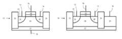
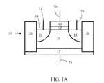
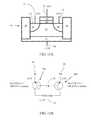
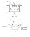
- FIG. 1Ais a schematic illustration of a memory cell according to an embodiment of the present invention.
- FIG. 1Bis a schematic illustration of a memory cell according to an embodiment of the present invention showing a contact to the substrate region.
- FIG. 2schematically illustrates multiple cells joined in an array to make a memory device according to an embodiment of the present invention.
- FIG. 3schematically illustrates n-p-n bipolar devices that are inherently formed in a memory cell according to an embodiment of the present invention.
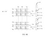
- FIG. 4Aillustrates segmenting of substrate terminals in an array according to an embodiment of the present invention.
- FIG. 4Bschematically illustrates multiplexers used to determine the biases applied to segmented substrate terminals according to an embodiment of the present invention.
- FIG. 4Cschematically illustrates use of a voltage generator circuitries to input positive bias to the multiplexers according to an embodiment of the present invention.
- FIG. 5graphically illustrates that the maximum charge stored in a floating body of a memory cell can be increased by applying a positive bias to the substrate terminal according to an embodiment of the present invention.
- FIG. 6Agraphs floating body potential as a function of floating body current and substrate potential according to an embodiment of the present invention.
- FIG. 6Bgraphs floating body potential as a function of floating body current and buried well potential according to an embodiment of the present invention.
- FIG. 7shows bias conditions for a selected memory cell and unselected memory cells in a memory array according to an embodiment of the present invention.
- FIG. 8Aillustrates an unselected memory cell sharing the same row as a selected memory cell during a read operation of the selected memory cell according to an embodiment of the present invention.
- FIG. 8Billustrates the states of the n-p-n bipolar devices of the unselected memory cell of FIG. 8A during the read operation of the selected memory cell according to the embodiment of FIG. 8A .
- FIG. 8Cillustrates an unselected memory cell sharing the same column as a selected memory cell during a read operation of the selected memory cell according to the embodiment of FIG. 8A .
- FIG. 8Dillustrates the states of the n-p-n bipolar devices of the unselected memory cell of FIG. 8C during the read operation of the selected memory cell according to the embodiment of FIG. 8A .
- FIG. 8Eillustrates an unselected memory cell that shares neither the same row nor the same column as a selected memory cell during a read operation of the selected memory cell according to the embodiment of FIG. 8A .
- FIG. 8Fillustrates the states of the n-p-n bipolar devices of the unselected memory cell of FIG. 8E during the read operation of the selected memory cell according to the embodiment of FIG. 8A .
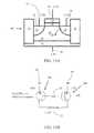
- FIG. 9is a schematic illustration of a write “0” operation to a memory cell according to an embodiment of the present invention.
- FIG. 10shows an example of bias conditions for a selected memory cell and unselected memory cells during a write “0” operation in a memory array according to an embodiment of the present invention.
- FIG. 11Aillustrates an example of bias conditions on unselected memory cells during a write “0” operation according to an embodiment of the present invention.
- FIG. 11Bshows an equivalent circuit diagram for the cell of FIG. 11A illustrating the intrinsic n-p-n bipolar devices.
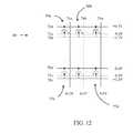
- FIG. 12shows bias conditions for selected and unselected memory cells of a memory array during a write “0” operation according to an embodiment of the present invention.
- FIG. 13Aillustrates an example of bias conditions on a selected memory cell during a write “0” operation according to an embodiment of the present invention.
- FIG. 13Bshows an equivalent circuit diagram for the cell of FIG. 13A illustrating the intrinsic n-p-n bipolar devices.
- FIG. 13Cillustrates an example of bias conditions on unselected memory cells sharing the same row as a selected memory cell in an array during a write “0” operation of the selected memory cell, according to the embodiment of FIG. 13A .
- FIG. 13Dshows an equivalent circuit diagram for the cell of FIG. 13C illustrating the intrinsic n-p-n bipolar devices.
- FIG. 13Eillustrates an example of bias conditions on unselected memory cells sharing the same column as a selected memory cell in an array during a write “0” operation of the selected memory cell, according to the embodiment of FIG. 13A .
- FIG. 13Fshows an equivalent circuit diagram for the cell of FIG. 13E illustrating the intrinsic n-p-n bipolar devices.
- FIG. 13Gillustrates an example of bias conditions on unselected memory cells that share neither the same row nor the same column as a selected memory cell in an array during a write “0” operation of the selected memory cell, according to the embodiment of FIG. 13A .
- FIG. 13Hshows an equivalent circuit diagram for the cell of FIG. 13G illustrating the intrinsic n-p-n bipolar devices.
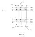
- FIG. 14illustrates an example of bias conditions of a selected memory cell and unselected memory cells in an array under a band-to-band tunneling write “1” operation of the selected cell according to an embodiment of the present invention.
- FIG. 15Aillustrates an example of bias conditions on the selected memory cell of FIG. 14 .
- FIG. 15Bshows an equivalent circuit diagram for the cell of FIG. 15A illustrating the intrinsic n-p-n bipolar devices.
- FIG. 15Cillustrates an example of bias conditions on unselected memory cells sharing the same row as a selected memory cell in an array during a write “1” operation of the selected memory cell, according to the embodiment of Fig. I 5 A.
- FIG. 15Dshows an equivalent circuit diagram for the cell of FIG. 15C illustrating the intrinsic n-p-n bipolar devices
- FIG. 15Eillustrates an example of bias conditions on unselected memory cells sharing the same column as a selected memory cell in an array during a write “1” operation of the selected memory cell, according to the embodiment of FIG. 15A .
- FIG. 15Fshows an equivalent circuit diagram for the cell of FIG. 15E illustrating the intrinsic ti-p-n bipolar devices.
- FIG. 15Gillustrates an example of bias conditions on unselected memory cells that share neither the same row nor the same column as a selected memory cell in an array during a write “1” operation of the selected memory cell, according to the embodiment of FIG. 15A .
- FIG. 15Hshows an equivalent circuit diagram for the cell of FIG. 15G illustrating the intrinsic n-p-n bipolar devices.
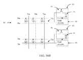
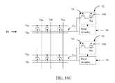
- FIG. 16Ashows a reference generator circuit which serves to generate the initial cumulative cell current of the memory cells sharing the same source line being written, according to an embodiment of the present invention.
- FIG. 16Bshows a reference generator circuit which serves to generate the initial cumulative cell current of the memory cells sharing the same source line being written, according to another embodiment of the present invention.
- FIG. 16Cshows a reference generator circuit which serves to generate the initial cumulative cell current of the memory cells sharing the same source line being written, according to another embodiment of the present invention.
- FIG. 17graphically illustrates that the potential of the floating body of a memory cell will increase over time as bias conditions are applied that will result in hole injection to the floating body, according to an embodiment of the present invention.
- FIG. 18Aschematically illustrates reference generator circuitry and read circuitry connected to a memory array according to an embodiment of the present invention.
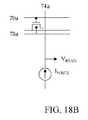
- FIG. 18Bshows a schematic of a voltage sensing circuitry configured to measure the voltage across the source line and the bit line terminals of a memory cell according to an embodiment of the present invention.
- FIG. 19illustrates bias conditions on a selected cell and unselected cells of an array during a read operation on the selected cell according to an embodiment of the present invention.
- FIG. 20illustrates bias conditions on a selected cell and unselected cells of an array during a write “0” operation on the selected cell according to an embodiment of the present invention.
- FIG. 21illustrates bias conditions on a selected cell and unselected cells of an array during a write “0” operation on the selected cell according to another embodiment of the present invention.
- FIG. 22illustrates bias conditions on a selected cell and unselected cells of an array during a band-to-band tunneling write “1” operation on the selected cell according to another embodiment of the present invention.
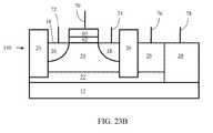
- FIG. 23Ais a schematic illustration of a memory cell according to another embodiment of the present invention.
- FIG. 23Bis a schematic illustration cell memory cell according to another embodiment of the present invention showing contacts to the buried well and substrate regions.
- FIG. 24schematically illustrates an array of memory cells of the type illustrated in FIG. 23 .
- FIG. 25schematically illustrates n-p-n bipolar devices inherent in the cell of FIG. 23 .
- FIG. 26illustrates an example of bias conditions on a array during performance of a read operation on a selected cell according to an embodiment of the present invention.
- FIG. 27illustrates bias conditions on a selected cell and unselected cells of an array during a write “0” operation on the selected cell according to an embodiment of the present invention.
- FIG. 28Aillustrates an example of bias conditions on the selected memory cell of FIG. 27 .
- FIG. 28Bshows an equivalent circuit diagram for the cell of FIG. 28A illustrating the intrinsic n-p-n bipolar devices.
- FIG. 28Cillustrates an example of bias conditions on unselected memory cells sharing the same row as a selected memory cell in an array during a write “0” operation of the selected memory cell, according to the embodiment of FIG. 27 .
- FIG. 28Dshows an equivalent circuit diagram for the cell of FIG. 28C illustrating the intrinsic n-p-n bipolar devices.
- FIG. 28Eillustrates an example of bias conditions on unselected memory cells sharing the same column as a selected memory cell in an array during a ii write “0” operation of the selected memory cell, according to the embodiment of FIG. 27 .
- FIG. 28Fshows an equivalent circuit diagram for the cell of FIG. 28E illustrating the intrinsic n-p-n bipolar devices.
- FIG. 28Gillustrates an example of bias conditions on unselected memory cells that share neither the same row nor the same column as a selected memory cell in an array during a write “0” operation of the selected memory cell, according to the embodiment of FIG. 27 .
- FIG. 28Hshows an equivalent circuit diagram for the cell of FIG. 28G illustrating the intrinsic n-p-n bipolar devices.
- FIG. 29illustrates an example of bias conditions applied to a selected memory cell under a band-to-hand tunneling write “1” operation according to an embodiment of the present invention.
- FIG. 30is a schematic illustration of a memory cell according to another embodiment of the present invention.
- FIG. 31is a schematic illustration of a memory cell according to another embodiment of the present invention.
- FIG. 32is a schematic illustration of a memory cell according to another embodiment of the present invention.
- FIG. 33is a schematic illustration of a memory cell according to another embodiment of the present invention.
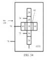
- FIG. 34is a top view, schematic illustration of a memory cell of FIGS. 30 and 32 .
- a “holding operation”, “standby operation” or “holding/standby operation”, as used herein,refers to a process of sustaining a state of a memory cell by maintaining the stored charge. Maintenance of the stored charge may be facilitated by applying a back bias to the cell in a manner described herein.
- a “a multi-level write operation”refers to a process that includes an ability to write more than more than two different states into a memory cell to store more than one bit per cell.
- a “write-then-verify” algorithm or operationrefers to a process where alternating write and read operations to a memory cell are employed to verify whether a desired memory state of the memory cell has been achieved during the write operation.
- a “read verify operation”refers to a process where a read operation is performed to verify whether a desired memory state of a memory cell has been achieved.
- a “read while programming” operationrefers to a process where simultaneous write and read operations can be performed to write a memory cell state.
- a “back bias terminal”refers to a terminal at the back side of a semiconductor transistor device, usually at the opposite side of the gate of the transistor.
- a back bias terminalis also commonly referred to as a “back gate terminal”.
- the back bias terminalrefers to the substrate terminal or the buried well terminal, depending upon the embodiment being described.
- back biasrefers to a voltage applied to a back bias terminal.
- the cell 50includes a substrate 12 of a first conductivity type, such as n-type conductivity type, for example.
- Substrate 12is typically made of silicon, but may comprise germanium, silicon germanium, gallium arsenide, carbon nanotubes, or other semiconductor materials known in the art.
- the substrate 12has a surface 14 .
- a first region 16 having a first conductivity type, such as n-type, for example,is provided in substrate 12 and which is exposed at surface 14 .
- a second region 18 having the first conductivity typeis also provided in substrate 12 , which is exposed at surface 14 and which is spaced apart from the first region 16 .
- First and second regions 16 and 18are formed by an implantation process formed on the material making up substrate 12 , according to any of implantation processes known and typically used in the art. Alternatively, a solid state diffusion process can be used to form first and second regions 16 and 18 .
- the floating body region 24can be formed by an implantation process formed on the material making up substrate 12 , or can be grown epitaxially.
- Insulating layers 26e.g. shallow trench isolation (STI)
- STIshallow trench isolation
- a gate 60is positioned in between the regions 16 and 18 , and above the surface 14 .
- the gate 60is insulated from surface 14 by an insulating layer 62 .
- Insulating layer 62may be made of silicon oxide and/or other dielectric materials, including high-K dielectric materials, such as, but not limited to, tantalum peroxide, titanium oxide, zirconium oxide, hafnium oxide, and/or aluminum oxide.
- the gate 60may be made of polysilicon material or metal gate electrode, such as tungsten, tantalum, titanium and their nitrides.
- Cell 50further includes word line (WL) terminal 70 electrically connected to gate 60 , source line (SL) terminal 72 electrically connected to one of regions 16 and 18 (connected to 16 as shown, but could, alternatively, be connected to 18 ), bit line (BL) terminal 74 electrically connected to the other of regions 16 and 18 (connected to 18 as shown, but could, alternatively, be connected to 16 when 72 is connected to 18 ), and substrate terminal 78 electrically connected to substrate 12 .
- WLword line
- SLsource line
- BLbit line
- Contact to substrate region 12can alternatively be made through region 20 having a first conductivity type, and which is electrically connected to substrate region 12 , as shown in FIG. 1B .
- the memory cell 50has a p-type conductivity type as the first conductivity type and n-type conductivity type as the second conductivity type, as noted above.
- a memory cell 50has been described for example in “Scaled 1T-Bulk Devices Built with CMOS 90 nm Technology for Low-cost eDRAM Applications”, R. Ranica, et al., pp. 38-41, Tech. Digest, Symposium on VLSI Technology, 2005, which is hereby incorporated herein, in its entirety, by reference thereto.
- the memory cell statesare represented by the charge in the floating body 24 . If cell 50 has holes stored in the floating body region 24 , then the memory cell 50 will have a lower threshold voltage (gate voltage where transistor is turned on) compared to when cell 50 does not store holes in floating body region 24 .
- the positive charge stored in the floating body region 24will decrease over time due to the p-n diode leakage formed by floating body 24 and regions 16 , 18 , and substrate 12 and due to charge recombination.
- a unique capability of the inventionis the ability to perform the holding operation in parallel to all memory cells 50 of the array 80 .
- the holding operationcan be performed by applying a positive back bias to the substrate terminal 78 while grounding terminal 72 and/or terminal 74 .
- the positive back bias applied to the substrate terminalwill maintain the state of the memory cells 50 that it is connected to.
- the holding operationis relatively independent of the voltage applied to terminal 70 . As shown in FIG.
- n-p-n bipolar devices 30 a and 30 bformed by substrate region 12 , floating body 24 , and SL and BL regions 16 . 18 . If floating body 24 is positively charged (i.e. in a state “1”), the bipolar transistor 30 a formed by SL region 16 , floating body 24 , and substrate region 12 and bipolar transistor 30 b formed by BL region 18 , floating body 24 , and substrate region 12 will be turned on.
- a fraction of the bipolar transistor currentwill then flow into floating region 24 (usually referred to as the base current) and maintain the state “1” data.
- the efficiency of the holding operationcan be enhanced by designing the bipolar device formed by substrate 12 , floating region 24 , and regions 16 , 18 to be a low-gain bipolar device, where the bipolar gain is defined as the ratio of the collector current flowing out of substrate terminal 78 to the base current flowing into the floating region 24 .
- the holding operationcan be performed in mass, parallel manner as the substrate terminal 78 (e.g., 78 a , 78 b , . . . , 78 n ) is typically shared by all the cells 50 in the memory array 80 .
- the substrate terminal 78can also be segmented to allow independent control of the applied bias on the selected portion of the memory array as shown in FIG. 4A , where substrate terminal 78 a , 78 b is shown segmented from substrate terminal 78 m , 78 n , for example. Also, because substrate terminal 78 is not used for memory address selection, no memory cell access interruption occurs due to the holding operation.
- a periodic pulse of positive voltagecan be applied to substrate terminal 78 , as opposed to applying a constant positive bias, in order to reduce the power consumption of the memory cell 50 .
- the state of the memory cell 50can be maintained by refreshing the charge stored in floating body 24 during the period over which the positive voltage pulse is applied to the back bias terminal (i.e., substrate terminal 78 ).
- FIG. 4Bfurther shows multiplexers 40 that determine the bias applied to substrate terminal 78 where the control signal could be the clock signal 42 or as will be described later, determined by different operating modes.
- the positive input signalscould be the power supply voltage Vcc ( FIG. 4B ) or a different positive bias could be generated by voltage generator circuitry 44 (see FIG. 4C ).
- the holding/standby operationalso results in a larger memory window by increasing the amount of charge that can be stored in the floating body 24 .
- the maximum potential that can be stored in the floating body 24is limited to the flat band voltage V FB as the junction leakage current to regions 16 and 18 increases exponentially at floating body potential greater than V FB .
- the bipolar actionresults in a hole current flowing into the floating body 24 , compensating for the junction leakage current between floating body 24 and regions 16 and 18 .
- the maximum charge V MC stored in floating body 24can be increased by applying a positive bias to the substrate terminal 78 as shown in FIG. 5 .
- the increase in the maximum charge stored in the floating body 24results in a larger memory window.
- the holding/standby operationcan also be used for multi-bit operations in memory cell 50 .
- a multi-level operationis typically used. This is done by dividing the overall memory window into different levels.
- the different memory statesare represented by different charges in the floating body 24 , as described for example in “The Multistable Charge-Controlled Memory Effect in SOI Transistors at Low Temperatures”, Tack et al., pp. 1373-1382, IEEE Transactions on Electron Devices, vol. 37, May 1990 and U.S. Pat. No.
- FIG. 6shows the floating body 24 relative net current for different floating body 24 potentials as a function of the voltage applied to substrate terminal 78 with BL, SL, and WL terminals 72 , 74 , and 70 , grounded.
- zero voltageis applied to substrate terminal 78
- no bipolar currentis flowing into the floating body 24 and as a result, the stored charge will leak over time.
- hole currentwill flow into floating body 24 and balance the junction leakage current to regions 16 and 18 .
- the junction leakage currentis determined by the potential difference between the floating body 24 and regions 16 and 18
- the bipolar current flowing into floating body 24is determined by both the substrate terminal 78 potential and the floating body 24 potential. As indicated in FIG.
- the current flowing into floating body 24is balanced by the junction leakage between floating body 24 and regions 16 and 18 .
- the different floating body 24 potentialsrepresent different charges used to represent different states of memory cell 50 . This shows that different memory states can be maintained by using the holding/standby operation described here.
- bias condition for the holding operationis hereby provided: zero voltage is applied to BL terminal 74 , zero voltage is applied to SL terminal 72 , zero or negative voltage is applied to WL terminal 70 , and a positive voltage is applied to the substrate terminal 78 .
- about 0.0 voltsis applied to terminal 72
- about 0.0 voltsis applied to terminal 74
- about 0.0 voltsis applied to terminal 70
- about +1.2 voltsis applied to terminal 78 .
- these voltage levelsmay vary.
- the charge stored in the floating body 24can be sensed by monitoring the cell current of the memory cell 50 . If cell 50 is in a state “1” having holes in the floating body region 24 , then the memory cell will have a lower threshold voltage (gate voltage where the transistor is turned on), and consequently a higher cell current, compared to if cell 50 is in a state “0” having no holes in floating body region 24 .
- a sensing circuit/read circuitry 90 typically connected to BL terminal 74 of memory array 80e.g., see read circuitry 90 in FIG. 18A ) can then be used to determine the data state of the memory cell.
- Examples of the read operationis described in “A Design of a Capacitorless IT-DRAM Cell Using Gate-Induced Drain Leakage (GIDL) Current for Low-power and High-speed Embedded Memory”, and Yoshida et al., pp. 913-918, International Electron Devices Meeting, 2003 and U.S. Pat. No. 7,301,803 “Bipolar reading technique for a memory cell having an electrically floating body transistor”, both of which are hereby incorporated herein, in their entireties, by reference thereto.
- An example of a sensing circuitis described in “An 18.5 ns 128 Mb SOI DRAM with a Floating body Cell”, Ohsawa et al., pp. 458-459, 609, IEEE International Solid-State Circuits Conference, 2005, which is hereby incorporated herein, in its entirety, by reference thereto.
- the read operationcan be performed by applying the following bias condition: a positive voltage is applied to the substrate terminal 78 , zero voltage is applied to SL terminal 72 , a positive voltage is applied to the selected BL terminal 74 , and a positive voltage greater than the positive voltage applied to the selected BL terminal 74 is applied to the selected WL terminal 70 .
- the unselected BL terminalswill remain at zero voltage and the unselected WL terminals will remain at zero or negative voltage.
- about 0.0 voltsis applied to terminal 72
- about +0.4 voltsis applied to the selected terminal 74
- about +1.2 voltsis applied to the selected terminal 70
- about +1.2 voltsis applied to terminal 78 .
- FIG. 7shows the bias conditions for the selected memory cell 50 a and unselected memory cells 50 b , 50 c , and 50 d in memory array 80 . However, these voltage levels may vary.
- the unselected memory cells 50 during read operationsare shown in FIGS. 8A , 8 C and 8 E, with illustration of the states of the n-p-n bipolar devices 30 a , 30 b inherent in the cells 50 of FIGS. 8A , 8 C and 8 E in FIGS. 8B , 8 D and 8 F, respectively.
- the bias conditions for memory cells 50 sharing the same row (e.g. memory cell 50 b ) and those sharing the same column (e.g. memory cell 50 c ) as the selected memory cell 50 aare shown in FIGS. 8A-8B and FIGS. 8C-8D , respectively, while the bias condition for memory cells 50 not sharing the same row or the same column as the selected memory cell 50 (e.g. memory cell 50 d ) is shown in FIGS. 8E-8F .
- both the SL terminal 72 and BL terminal 74are at about 0.0 volts ( FIGS. 8A-8B ). As can be seen, these cells will be at holding mode, with memory cells in state “1” and will maintain the charge in floating body 24 because the intrinsic n-p-n bipolar devices 30 a , 30 b will generate hole current to replenish the charge in floating body 24 ; while memory cells 50 in state “0” will remain in the neutral state.
- a positive voltageis applied to the BL terminal 74 ( FIGS. 8C-8D ).
- the n-p-n bipolar device 30 a formed by substrate 12 , floating body 24 , and region 16will still maintain the state of the floating body 24 as the SL terminal 72 connected to region 16 is grounded.
- both the SL terminal 72 and BL terminal 74are at about 0.0 volts ( FIGS. 8E-8F ). As can be seen, these cells will be at holding mode, where memory cells in state “1” will maintain the charge in floating body 24 because the intrinsic n-p-n bipolar devices 30 a , 30 b will generate holes current to replenish the charge in floating body 24 ; while memory cells in state “0” will remain in the neutral state.
- the holding operationdoes not interrupt the read operation of the memory cells 50 .
- the unselected memory cells 50 during a read operationwill remain in a holding operation.
- a write “0” operation of the cell 50is described with reference to FIG. 9 .
- a negative biasis applied to SL terminal 72
- zero or negative voltageis applied to WL terminal 70
- zero or positive voltageis applied to substrate terminal 78 .
- the SL terminal 72 for the unselected cellswill remain grounded. Under these conditions, the p-n junction between 24 and 16 is forward-biased, evacuating any holes from the floating body 24 .
- about ⁇ 2.0 voltsis applied to terminal 72
- about 0.0 voltsis applied to terminal 70
- about +1.2 voltsis applied to terminal 78 .
- these voltage levelsmay vary, while maintaining the relative relationships between the charges applied, as described above.
- FIG. 10shows an example of bias conditions for the selected and unselected memory cells 50 during a write “0” operation in memory array 80 .
- the negative bias applied to SL terminal 72causes large potential difference between floating body 24 and region 16 .
- the hole current generated by the intrinsic n-p-n bipolar devices 30 a , 30 bwill not be sufficient to compensate for the forward bias current of p-n diode formed by floating body 24 and junction 16 .
- FIGS. 11A-11BAn example of bias conditions and an equivalent circuit diagram illustrating the intrinsic n-p-n bipolar devices 30 a , 30 b of unselected memory cells 50 during write “0” operations are illustrated in FIGS. 11A-11B . Since the write “0” operation only involves applying a negative voltage to the SL terminal 72 , the bias conditions for all the unselected cells are the same. As can be seen, the unselected memory cells will be in a holding operation, with both BL and SL terminals at about 0.0 volts. The positive back bias applied to the substrate terminal 78 employed for the holding operation does not interrupt the write “0” operation of the selected memory cells. Furthermore, the unselected memory cells remain in the holding operation.
- the write “0” operation referred to abovehas a drawback in that all memory cells 50 sharing the same SL terminal will be written to simultaneously and as a result, this does not allow individual bit writing, i.e., writing to a single cell 50 memory bit.
- write “0”is first performed on all the memory cells, followed by write “1” operations on a selected bit or selected bits.
- An alternative write “0” operation that allows for individual bit writingcan be performed by applying a positive voltage to WL terminal 70 , a negative voltage to BL terminal 74 , zero or positive voltage to SL terminal 72 , and zero or positive voltage to substrate terminal 78 .
- the floating body 24 potentialwill increase through capacitive coupling from the positive voltage applied to the WL terminal 70 .
- the p-n junction between 24 and 18is forward-biased, evacuating any holes from the floating body 24 .
- the applied potentialcan be optimized as follows: if the floating body 24 potential of state “1” is referred to as V FB1 , then the voltage applied to the WL terminal 70 is configured to increase the floating body 24 potential by V FB1 /2 while -V FB1 /2 is applied to BL terminal 74 . A positive voltage can be applied to SL terminal 72 to further reduce the undesired write “0” disturb on other memory cells 50 in the memory array. The unselected cells will remain at holding state, i.e. zero or negative voltage applied to WL terminal 70 and zero voltage applied to BL terminal 74 .
- the following bias conditionsare applied to the selected memory cell 50 a : a potential of about 0.0 volts is applied to terminal 72 , a potential of about ⁇ 0.2 volts is applied to terminal 74 , a potential of about +0.5 volts is applied to terminal 70 , and about +1.2 volts is applied to terminal 78 ; while about 0.0 volts is applied to terminal 72 , about 0.0 volts is applied to terminal 74 , about 0.0 volts is applied to terminal 70 , and about +1.2 volts is applied to terminal 78 of the unselected memory cells.
- FIG. 12shows the bias conditions for the selected and unselected memory cells in memory array 80 . However, these voltage levels may vary.
- FIGS. 13A-13BThe bias conditions of the selected memory cell 50 a under write “0” operation are further elaborated and are shown in FIGS. 13A-13B .
- the potential difference between floating body 24 and junction 18(connected to BL terminal 74 ) is now increased, resulting in a higher forward bias current than the base hole current generated by the n-p-n bipolar devices 30 a , 30 b formed by substrate 12 , floating body 24 , and regions 16 and 18 .
- the net resultis that holes will be evacuated from floating body 24 .
- the unselected memory cells 50 during write “0” operationsare shown in FIGS. 13C-13H .
- the bias conditions for memory cells sharing the same rowe.g. memory cell 50 b
- FIGS. 13C-13DThe bias conditions for memory cells sharing the same row (e.g. memory cell 50 b ) are illustrated in FIGS. 13C-13D
- the bias conditions for memory cells sharing the same columne.g. memory cell 50 c
- FIGS. 13E-13Fthe bias conditions for memory cells not sharing the same row or the same column (e.g. memory cell 50 d ) as the selected memory cell 50 are shown in FIGS. 13G-13H .
- both the SL terminal 72 and BL terminal 74are at about 0.0 volts ( FIGS. 13C and 13D ).
- the floating body 24 potential of these cellswill also increase due to capacitive coupling from the WL terminal 70 .
- the increase in the floating body 24 potentialis not sustainable as the forward bias current of the p-n diodes formed by floating body 24 and junctions 16 and 18 is greater than the base hole current generated by the n-p-n bipolar device 30 formed by substrate 12 , floating body 24 , and junctions 16 and 18 .
- the floating body 24 potentialwill return to the initial state “1” equilibrium potential.
- the hole current of the n-p-n bipolar device 30 b formed by substrate 12 , floating body 24 , and region 18will also increase as a result of the increase in potential difference between the substrate 12 and region 18 (the collector and emitter terminals, respectively).
- the floating body 24 of memory cells in state “1”will also remain positively charged (i.e., in state “1”).
- both the SL terminal 72 and BL terminal 74are at about 0.0 volts (see FIGS. 13G and 13H ). These cells will thus be in a holding mode and continue a holding operation, with memory' cells in state “1” maintaining the charge in floating body 24 because the intrinsic n-p-n bipolar device 30 will generate hole current to replenish the charge in floating body 24 ; while memory cells in state “0” will remain in the neutral state.
- the present inventionprovides for a write “0” operation that allows for bit selection.
- the positive bias applied to the substrate terminal 78 of the memory cells 50is necessary to maintain the states of the unselected cells 50 , especially those sharing the same row and column as the selected cells 50 , as the bias conditions can potentially alter the states of the memory cells 50 without the intrinsic bipolar devices 30 a , 30 b (formed by substrate 12 , floating body 24 , and regions 16 , 18 , respectively) re-establishing the equilibrium condition.
- the positive bias applied to the substrate terminal 78 employed for the holding operationdoes not interrupt the write “0” operation of the selected memory cell(s).
- a write “1” operationcan be performed on memory cell 50 through impact ionization or band-to-band tunneling mechanism, as described for example in “A Design of a Capacitorless 1T-DRAM Cell Using Gate-Induced Drain Leakage (GIRL) Current for Low-power and High-speed Embedded Memory”, Yoshida et al., pp. 913-918, International Electron Devices Meeting, 2003, which was incorporated by reference above.
- GIRLGate-Induced Drain Leakage
- FIG. 14 and FIGS. 15A-15BAn example of the bias condition of the selected memory cell 50 under band-to-band tunneling write “1” operation is illustrated in FIG. 14 and FIGS. 15A-15B .
- the negative bias applied to the WL terminal 70 and the positive bias applied to the BL terminal 74results in hole injection to the floating body 24 of the selected memory cell 50 .
- the positive bias applied to the substrate terminal 78maintains the resulting positive charge on the floating body 24 as discussed above.
- the unselected cells 50remain at the holding mode, with zero or negative voltage applied to the unselected WL terminal 70 and zero voltage is applied to the unselected BL terminal 74 to maintain the holding operation (holding mode).
- the following bias conditionsare applied to the selected memory cell 50 a : a potential of about 0.0 volts is applied to terminal 72 , a potential of about +1.2 volts is applied to terminal 74 , a potential of about ⁇ 1.2 volts is applied to terminal 70 , and about +1.2 volts is applied to terminal 78 ; and the following bias conditions are applied to the unselected memory cells 50 : about 0.0 volts is applied to terminal 72 , about 0.0 volts is applied to terminal 74 , about 0.0 volts is applied to terminal 70 , and about +1.2 volts is applied to terminal 78 .
- FIG. 14shows the bias conditions for the selected and unselected memory cells in memory array 80 . However, these voltage levels may vary.
- FIGS. 15C-15HThe unselected memory cells during write “1” operations are shown in FIGS. 15C-15H .
- the bias conditions for memory cells sharing the same rowe.g. memory cell 50 b
- FIGS. 15C-15DThe bias conditions for memory cells sharing the same column as the selected memory cell 50 a
- FIGS. 15E-15FThe bias conditions for memory cells 50 not sharing the same row or the same column as the selected memory cell 50 a (e.g. memory cell 50 d ) are shown in FIGS. 15G-15H .
- both the SL terminal 72 and BL terminal 74are at about 0.0 volts, with the WL terminal 70 at zero or negative voltage ( FIGS. 15C-15D ). Comparing with the holding operation bias condition, it can be seen that cells sharing the same row (i.e. the same WL terminal 70 ) are in holding mode. As a result, the states or these memory cells will remain unchanged.
- a positive voltageis applied to the BL terminal 74 .
- the bipolar device 30 b formed by substrate 12 , floating body 24 , and region 18 connected to BL terminal 74will be turned off because of the small voltage difference between the substrate terminal 78 and BL terminal 74 (the collector and emitter terminals, respectively).
- the bipolar device 30 a formed by substrate 12 , floating body 24 , and region 16 connected to SL terminal 72will still generate base hole current for memory cells in state “1” having positive charge in floating body 24 .
- Memory cells in state “0”will remain in state “0” as this bipolar device 30 a (formed by substrate 12 , floating body 24 , and region 16 ) is off.
- both the SL terminal 72 and BL terminal 74are at about 0.0 volts (see FIGS. 15G-15H ). As can be seen, these cells will be in a holding operation (holding mode), where memory cells in state “1” will maintain the charge in floating body 24 because the intrinsic n-p-n bipolar devices 30 a , 30 b will generate hole current to replenish the charge in floating body 24 ; while memory cells in state “0” will remain in the neutral state.
- the positive bias applied to the substrate terminal 78 employed for the holding operationdoes not interrupt the write “1” operation of the selected memory cell(s). At the same time, the unselected memory cells during write “1” operation will remain in holding operation.
- a multi-level write operationcan be performed using an alternating write and verify algorithm, where a write pulse is first applied to the memory cell 50 , followed by a read operation to verify if the desired memory state has been achieved. If the desired memory state has not been achieved, another write pulse is applied to the memory cell 50 , followed by another read verification operation. This loop is repeated until the desired memory state is achieved.
- a positive voltageis applied to BL terminal 74
- zero voltageis applied to SL terminal 72
- a negative voltageis applied to WL terminal 70
- a positive voltageis applied to the substrate terminal 78 .
- Positive voltages of different amplitudeare applied to BL terminal 74 to write different states to floating body 24 .
- the resulting floating body 24 potentialis maintained through base hole current flowing into floating body 24 .
- the write operationis performed by applying the following bias condition: a potential of about 0.0 volts is applied to terminal 72 , a potential of about ⁇ 1.2 volts is applied to terminal 70 , and about +1.2 volts is applied to terminal 78 , while the potential applied to BL terminal 74 is incrementally raised. For example, in one non-limiting embodiment 25 millivolts is initially applied to BL terminal 74 , followed by a read verify operation. If the read verify operation indicates that the cell current has reached the desired state (i.e., cell current corresponding to whichever of 00, 01, 10 or 11 is desired is achieved), then the multi write operation is commenced.
- the desired statei.e., cell current corresponding to whichever of 00, 01, 10 or 11 is desired is achieved
- the voltage applied to BL terminal 74is raised, for example, by another 25 millivolts, to 50 millivolts. This is subsequently followed by another read verify operation, and this process iterates until the desired state is achieved. However, the voltage levels described may vary. The write operation is followed by a read operation to verify the memory state.
- the write-then-verify algorithmis inherently slow since it requires multiple write and read operations.
- the present inventionprovides a multi-level write operation that can be performed without alternate write and read operations. This is accomplished by ramping the voltage applied to BL terminal 74 , while applying zero voltage to SL terminal 72 , a positive voltage to WL terminal 70 , and a positive voltage to substrate terminal 78 of the selected memory cells. The unselected memory cells will remain in holding mode, with zero or negative voltage applied to WL terminal 70 and zero voltage applied to BL terminal 74 . These bias conditions will result in a hole injection to the floating body 24 through impact ionization mechanism.
- the state of the memory cell 50can be simultaneously read for example by monitoring the change in the cell current through a read circuitry 90 ( FIGS.
- the cell current measured in the source line directionis a cumulative cell current of all memory cells 50 which share the same source line 72 (see FIGS. 16A-16C ). As a result, only one memory cell 50 sharing the same source line 72 can be written. This ensures that the change in the cumulative cell current is a result of the write operation on the selected memory cell 50 .
- the potential of the floating body 24increases over time as these bias conditions result in hole injection to floating body 24 through an impact ionization mechanism.
- the voltage applied to BL terminal 74can be removed.
- the resulting floating body 24 potentialis maintained through base hole current flowing into floating body 24 . In this manner, the multi-level write operation can be performed without alternate write and read operations.
- FIGS. 16A-16Calso show a reference generator circuit 92 , which serves to generate the initial cumulative cell current of the memory cells 50 sharing the same source line 72 being written.
- the cumulative charge of the initial state for all memory cells 50 sharing the same source line 72can be stored in a capacitor 94 (see FIG. 16B ).
- Transistor 96is turned on when charge is to be written into or read from capacitor 94 .
- a reference cell 50 RFIG. 16C
- Transistor 96is turned on when charge is to be written into or read from capacitor 94 .
- a reference cell 50 RFIG. 16C
- Transistor 96is turned on when a write operation is to be performed on the reference cell 50 R.
- a positive biasis also applied to the substrate of the reference cell to maintain its state.
- the size of the reference cell 50 Rneeds to be configured such that it is able to store the maximum cumulative charge of all the memory cells 50 , i.e. when all of the memory cells 50 sharing the same source line 72 are positively charged.
- a multi-level write operation using an impact ionization mechanismcan be performed by ramping the write current applied to BL terminal 74 instead of ramping the BL terminal 74 voltage.
- a multi-level write operationcan be performed through a band-to-band tunneling mechanism by ramping the voltage applied to BL terminal 74 , while applying zero voltage to SL terminal 72 , a negative voltage to WL terminal 70 , and zero or positive voltage to substrate terminal 78 of the selected memory cells 50 .
- the unselected memory cells 50will remain in holding mode, with zero or negative voltage applied to WL terminal 70 and zero voltage applied to BL terminal 74 .
- multiple BL terminals 74can be simultaneously selected to write multiple cells in parallel. The potential of the floating body 24 of the selected memory cell(s) 50 will increase as a result of the band-to-band tunneling mechanism.
- the state of the selected memory cell(s) 50can be simultaneously read for example by monitoring the change in the cell current through a read circuitry 90 coupled to the source line. Once the change in the cell current reaches the desired level associated with a state of the memory cell, the voltage applied to BL terminal 74 can be removed. If positive voltage is applied to substrate terminal 78 , the resulting floating body 24 potential is maintained through base hole current flowing into floating body 24 . In this manner, the multi-level write operation can be performed without alternate write and read operations.
- the multi-level write operation using band-to-band tunneling mechanismcan also be performed by ramping the write current applied to BL terminal 74 instead of ramping the voltage applied to BL terminal 74 .
- a read while programming operationcan be performed by monitoring the change in cell current in the bit line direction through a reading circuitry 90 coupled to the bit line 74 as shown in FIG. 18A .
- Reference cells 50 Rrepresenting different memory states are used to verify the state of the write operation
- the reference cells 50 Rcan be configured through a write-then-verify operation for example when the memory device is first powered up.
- the resulting cell current of the memory cell 50 being writtenis compared to the reference cell 50 R current by means of the read circuitry 90 .
- the reference cell 50 Ris also being biased at the same bias conditions applied to the selected memory cell 50 during the write operation. Therefore, the write operation needs to be ceased after the desired memory state is achieved to prevent altering the state of the reference cell 50 R.
- the voltage at the bit line 74can be sensed instead of the cell current.
- the bit line voltagecan be sensed for example using a voltage sensing circuitry (see FIG. 18B ) as described in “VLSI Design of Non-Volatile Memories”, Campardo G. et al., 2005, which is hereby incorporated herein, in its entirety, by reference thereto.
- the bias conditions described aboveare applied both to the selected memory cell 50 and to the “01” reference cell 50 R: zero voltage is applied to the source line terminal 72 , a positive voltage is applied to the substrate terminal 78 , a positive voltage is applied to the WL terminal 70 (for the impact ionization mechanism), while the BL terminal 74 is being ramped up, starting from zero voltage. Starting the ramp voltage from a low voltage (i.e. zero volts) ensures that the state of the reference cell 50 R does not change.
- the voltage applied to the BL terminal 74is then increased. Consequently, holes are injected into the floating body 24 of the selected cell 50 and subsequently the cell current of the selected cell 50 increases. Once the cell current of the selected cell 50 reaches that of the “01” reference cell, the write operation is stopped by removing the positive voltage applied to the BL terminal 74 and WL terminal 70 .
- a periodic pulse of positive voltagecan be applied to substrate terminal 78 , as opposed to applying a constant positive bias, to reduce the power consumption of the memory cell 50 .
- the memory cell 50 operations during the period where the substrate terminal 78 is being groundedare now briefly described. During the period when the substrate terminal 78 is grounded, the memory cells 50 connected to a ground substrate terminal 78 are no longer in holding mode. Therefore the period during which the substrate terminal is grounded must be shorter than the charge retention time period of the floating body, to prevent the state of the floating body from changing when the substrate terminal is grounded.
- the charge lifetime (i.e., charge retention time period) of the floating body 24 without use of a holding modehas been shown to be on the order of milliseconds, for example, see “A Scaled Floating Body Cell (FBC) Memory with High-k+Metal Gate on Thin-Silicon and Thin-BOX for 16-nm Technology Node and Beyond”, Ban et al., pp. 92-92, Symposium on VLSI Technology, 2008, which is hereby incorporated herein, in its entirety, by reference thereto.
- the state of the memory cell 50can be maintained by refreshing the charge stored in floating body 24 during the period over which the positive voltage pulse is applied to the back bias terminal (i.e., substrate terminal 78 ).
- a read operationcan be performed by applying the following bias conditions: zero voltage is applied to the substrate terminal 78 , zero voltage is applied to SL terminal 72 , a positive voltage is applied to the selected BL terminal 74 , and a positive voltage greater than the positive voltage applied to the selected BL terminal 74 is applied to the selected WL terminal 70 .
- the unselected BL terminals 74will remain at zero voltage and the unselected WL terminals 70 will remain at zero or negative voltage. If the substrate terminals 78 are segmented (as for example shown in FIGS. 4A-4C ), a positive voltage can he applied to the unselected substrate terminals 78 .
- about 0.0 voltsis applied to terminal 72
- about +0.4 voltsis applied to the selected terminal 74
- about +1.2 voltsis applied to the selected terminal 70
- about 0.0 voltsis applied to terminal 78 .
- the unselected terminals 74remain at 0.0 volts and the unselected terminals 70 remain at 0.0 volts.
- the unselected terminals 78(in the case where the substrate terminals 78 are segmented as in FIGS. 4A and 4B ) can remain at +1.2 volts (see FIG. 19 ).
- the read operationis carried out over a time period on the order of nanoseconds, it is of a much shorter duration than the charge lifetime (charge retention time period) of the floating body 24 unassisted by a holding operation. Accordingly, the performance of a read operation does not affect the states of the memory cells connected to the terminal 78 as it is momentarily (on the order of nanoseconds) grounded.
- a write “0” operation of the cell 50can be performed by applying the following bias conditions: a negative bias is applied to SL terminal 72 , zero or negative voltage is applied to WL terminal 70 , and zero voltage is applied to substrate terminal 78 .
- the SL terminal 72 for the unselected cellswill remain grounded. If the substrate terminals 78 are segmented (as for example shown in FIGS. 4A-4C ), a positive voltage can be applied to the unselected substrate terminals 78 . Under these conditions, the p-n junction between 24 and 16 is forward-biased, evacuating any holes from the floating body 24 .
- about ⁇ 2.0 voltsis applied to terminal 72
- about 0.0 voltsis applied to terminal 70
- about 0.0 voltsis applied to terminal 78 .
- the unselected terminals 78(in the case where the substrate terminals 78 are segmented as in FIGS. 4A and 4B ) can remain at +1.2 volts. With the substrate terminal 78 being grounded, there is no bipolar hole current flowing to the floating body 24 . As a result, the write “0” operation will also require less time. Because the write “0” operation is brief, occurring over a time period on the order of nanoseconds, it is of much shorter duration than the charge retention time period of the floating body 24 , unassisted by a holding operation.
- the write “0” operationdoes not affect the states of the unselected memory cells 50 connected to the terminal 78 being momentarily grounded to perform the write “0” operation.
- the bias conditions applied to the memory array 80are shown in FIG. 20 . However, these voltage levels may vary, while maintaining the relative relationships between the charges applied, as described above.
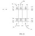
- FIG. 21An example of the bias conditions for an alternative write “0” operation which allows for individual bit write is shown in FIG. 21 .
- the following conditionsare applied to selected memory cell 50 : a positive voltage to WL terminal 70 , a negative voltage to BL terminal 74 , zero or positive voltage to SL terminal 72 , and zero voltage to substrate terminal 78 .
- the floating body 24 potentialwill increase through capacitive coupling from the positive voltage applied to the WL terminal 70 .
- the p-n junction between 24 and 18is forward-biased, evacuating any holes from the floating body 24 .
- the applied potentialcan be optimized as follows: if the floating body 24 potential of state “1” is referred to as V FB1 , then the voltage applied to the WL terminal 70 is configured to increase the floating body 24 potential by V FB1 /2 while ⁇ V FB1 /2 is applied to BL terminal 74 . A positive voltage can be applied to SL terminal 72 to further reduce the undesired write “0” disturb on other memory cells 50 in the memory array that doe not share the same common SL terminal 72 as the selected memory cell. The unselected cells will remain at holding state, i.e.
- the write “0” operationis brief, occurring over a time period on the order of nanoseconds, it is of much shorter duration than the charge retention time period of the floating body 24 , unassisted by a holding operation. Accordingly, the write “0” operation does not affect the states of the unselected memory cells 50 connected to the terminal 78 being momentarily grounded to perform the write “0” operation.
- the following bias conditionsare applied to the selected memory cell 50 a : a potential of about 0.0 volts is applied to terminal 72 a , a potential of about ⁇ 0.2 volts is applied to terminal 74 a , a potential of about +0.5 volts is applied to terminal 70 a , and about 0.0 volts is applied to terminal 78 a ; while about 0.0 volts is applied to terminal 72 n and the other SL terminals not connected to the selected cell 50 a , about 0.0 volts is applied to terminal 74 n and the other BL terminals not connected to the selected cell 50 a , about 0.0 volts is applied to terminal 70 n and the other WL terminals not connected to the selected cell 50 a , and about +1.2 volts is applied to terminal 78 n and the other substrate terminals not connected to the selected cell 50 a .
- these voltage levelsmay vary.
- FIG. 22An example of the'bias conditions applied to the memory array 80 under a band-to-band tunneling write “1” operation to cell 50 a is shown in FIG. 22 , where a negative bias is applied to WL terminal 70 a , a positive bias is applied to BL terminal 74 a , zero voltage is applied to SL terminal 72 a , and zero voltage is applied to substrate terminal 78 a .
- the negative bias applied to the WL terminal 70 a and the positive bias applied to the BL terminal 74 awill result in hole injection to the floating body 24 of the selected memory cell 50 a .
- the unselected cells 50will remain at the holding mode, with zero or negative voltage applied to the unselected WL terminals 70 (in this case, terminal 70 n and any other WL terminal 70 not connected to selected cell 50 a ) and zero voltage is applied to the unselected BL terminals 74 (in this case, terminals 74 b , 74 n and any other BL terminal 74 not connected to selected cell 50 a ) and positive voltage applied to unselected substrate terminals 78 (in the case the substrate terminals 78 are segmented as for example shown in FIGS. 4A and 4B ; and, in FIG. 22 , to terminals 78 n and any other substrate terminals 78 not connected to selected cell 50 a ).
- the following bias conditionsare applied to the selected memory cell 50 a : a potential of about 0.0 volts is applied to terminal 72 a , a potential of about +1.2 volts is applied to terminal 74 a , a potential of about ⁇ 1.2 volts is applied to terminal 70 a , and about 0.0 volts is applied to terminal 78 a ; while about 0.0 volts is applied to the unselected terminals 72 (defined in the preceding paragraph), about 0.0 volts is applied to unselected terminals 74 (defined in the preceding paragraph), about 0.0 volts is applied to unselected terminals 70 (defined in the preceding paragraph), and about +1.2 volts is applied to unselected substrate terminals 78 (defined in the preceding paragraph) of the unselected memory cells.
- these voltage levelsmay vary.
- FIG. 23Ashows another embodiment of a memory cell 150 according to the present invention.
- the cell 150includes a substrate 12 of a first conductivity type, such as a p-type conductivity type, for example.
- Substrate 12is typically made of silicon, but may comprise germanium, silicon germanium, gallium arsenide, carbon nanotubes, or other semiconductor materials known in the art.
- the substrate 12has a surface 14 .
- a first region 16 having a second conductivity type, such as n-type, for example,is provided in substrate 12 and is exposed at surface 14 .
- a second region 18 having the second conductivity typeis also provided in substrate 12 , and is also exposed at surface 14 .
- Second region 18is spaced apart from the first region 16 , as shown.
- First and second regions 16 and 18may be formed by an implantation process on the material making up substrate 12 , according to any of implantation processes known and typically used in the art. Alternatively, a solid state diffusion process may be used to form first and second regions 16 and
- a buried layer 22 of the second conductivity typeis also provided in the substrate 12 , buried in the substrate 12 , as shown. Buried layer 22 may also be formed by an ion implantation process on the material of substrate 12 . Alternatively, buried layer 22 can be grown epitaxially.
- a floating body region 24 of the substrate 12 having a first conductivity type, such as a p-type conductivity type,is bounded by surface, first and second regions 16 , 18 , insulating layers 26 and buried layer 22 .
- Insulating layers 26e.g., shallow trench isolation (STI)
- Insulating layers 26may be made of silicon oxide, for example. Insulating layers 26 insulate cell 150 from neighboring cells 150 when multiple'cells 150 are joined in an array 180 to make a memory device as illustrated in FIG.
- a gate 60is positioned in between the regions 16 and 18 , and above the surface 14 .
- the gate 60is insulated from surface 14 by an insulating layer 62 .
- Insulating layer 62may be made of silicon oxide and/or other dielectric materials, including high-K dielectric materials, such as, but not limited to, tantalum peroxide, titanium oxide, zirconium oxide, hafnium oxide, and/or aluminum oxide.
- the gate 60may be made of polysilicon material or metal gate electrode, such as tungsten, tantalum, titanium and their nitrides.
- Cell 150further includes word line (WL) terminal 70 electrically connected to gate 60 , source line (SL) terminal 72 electrically connected to one of regions 16 and 18 (connected to 16 as shown, but could, alternatively, be connected to 18 ), bit line (BL) terminal 74 electrically connected to the other of regions 16 and 18 , buried well (BW) terminal 76 electrically connected to buried layer 22 , and substrate terminal 78 electrically connected to substrate 12 at a location beneath buried layer 22 .
- WLword line
- SLsource line
- BLbit line
- BWburied well
- Contact to buried well region 22can be made through region 20 having a second conductivity type, and which is electrically connected to buried well region 22
- contact to substrate region 12can be made through region 28 having a first conductivity type, and which is electrically connected to substrate region 12 , as shown in FIG. 23B .
- the memory cell 150may be provided with p-type conductivity type as the first conductivity type and n-type conductivity type as the second conductivity type.
- n-p-n bipolar devices 130 a , 130 bformed by buried well region 22 , floating body 24 , and SL and BL regions 16 , 18 .
- the memory cell operationswill be described as follows. As will be seen, the operation principles of this embodiment of the memory cell 150 will follow the descriptions above, where the bias applied on the n-type substrate terminal 78 for the above described memory cell 50 is now applied to the n-type buried well terminal 76 of cell 150 .
- the p-type substrate 12 of the current embodiment of the memory cell 150will be grounded, reverse biasing the p-n junction between substrate 12 and buried well layer 22 , thereby preventing any leakage current between substrate 12 and buried well layer 22 .
- a holding operationcan be performed by applying a positive back bias to the BW terminal 76 while grounding terminal 72 and/or terminal 74 . If floating body 24 is positively charged (i.e. in a state “1”), the bipolar transistor formed by SL region 16 , floating body 24 , and buried well region 22 and bipolar transistor formed by BL region 18 , floating body 24 , and buried well region 22 will be turned on.
- a fraction of the bipolar transistor currentwill then flow into floating region 24 (usually referred to as the base current) and maintain the state “1” data.
- the efficiency of the holding operationcan be enhanced by designing the bipolar devices 130 a , 130 b formed by buried well layer 22 , floating region 24 , and regions 16 / 18 to be a low-gain bipolar device, where the bipolar gain is defined as the ratio of the collector current flowing out of BW terminal 76 to the base current flowing into the floating region 24 .
- the holding operationcan be performed in mass, parallel manner as the BW terminal 76 (functioning as back bias terminal) is typically shared by all the cells 150 in the memory array 180 , or at least by multiple cells 150 in a segment of the array 180 .
- the BW terminal 76can also be segmented to allow independent control of the applied bias on a selected portion of the memory array 180 . Also, because BW terminal 76 is not used for memory address selection, no memory cell access interruption occurs due to the holding operation.
- An example of the bias conditions applied to cell 150 to carry out a holding operationincludes: zero voltage is applied to BL terminal 74 , zero voltage is applied to SL terminal 72 , zero or negative voltage is applied to WL terminal 70 , a positive voltage is applied to the BW terminal 76 , and zero voltage is applied to substrate terminal 78 .
- about 0.0 voltsis applied to terminal 72
- about 0.0 voltsis applied to terminal 74
- about 0.0 voltsis applied to terminal 70
- about +1.2 voltsis applied to terminal 76
- about 0.0 voltsis applied to terminal 78 .
- these voltage levelsmay vary.
- a read operationcan be performed on cell 150 by applying the following bias conditions: a positive voltage is applied to the BW terminal 76 , zero voltage is applied to SL terminal 72 , a positive voltage is applied to the selected BL terminal 74 , and a positive voltage greater than the positive voltage applied to the selected BL terminal 74 is applied to the selected WL terminal 70 , while zero voltage is applied to substrate terminal 78 .
- the unselected BL terminals 74e.g., 74 b , . . .
- the unselected WL terminals 70(e.g., 70 n and any other WL terminals 70 not connected to selected cell 150 a ) will remain at zero or negative voltage.
- about 0.0 voltsis applied to terminal 72
- about +0.4 voltsis applied to the selected terminal 74 a
- about +1.2 voltsis applied to the selected terminal 70 a
- about +1.2 voltsis applied to terminal 76
- about 0.0 voltsis applied to terminal 78 , as illustrated in FIG. 26 .
- the unselected terminals 74remain at 0.0 volts and the unselected terminal 70 remain at 0.0 volts as illustrated in FIG. 26 .
- the unselected memory cells( 150 b , 150 c and 150 d ) will be at holding mode, maintaining the states of the respective floating bodies 24 thereof. Furthermore, the holding operation does not interrupt the read operation of the selected memory cell 150 a.
- a negative biasis applied to SL terminal 72 , zero or negative voltage is applied to WL terminal 70 , zero or positive voltage is applied to BW terminal 76 , and zero voltage is applied to substrate terminal 78 .
- the SL terminal 72 for the unselected cells 150 that are not commonly connected to the selected cell 150 awill remain grounded. Under these conditions, the p-n junctions (junction between 24 and 16 and between 24 and 18 ) are forward-biased, evacuating any holes from the floating body 24 .
- about ⁇ 2.0 voltsis applied to terminal 72
- about ⁇ 1.2 voltsis applied to terminal 70
- about +1.2 voltsis applied to terminal 76
- about 0.0 voltsis applied to terminal 78 .
- these voltage levelsmay vary, while maintaining the relative relationships between the charges applied, as described above.
- the bias conditions for all the unselected cellsare the same since the write “0” operation only involves applying a negative voltage to the SL terminal 72 (thus to the entire row). As can be seen, the unselected memory cells will be in holding operation, with both BL and SL terminals at about 0.0 volts.
- the holding operationdoes not interrupt the write “0” operation of the memory cells. Furthermore, the unselected memory cells will remain in holding operation during a write “0” operation.
- An alternative write “0”. operationwhich, unlike the previous write “0” operation described above, allows for individual bit write, can be performed by applying a positive voltage to WL terminal 70 , a negative voltage to BL terminal 74 , zero or positive voltage to SL terminal 72 , zero or positive voltage to BW terminal 76 , and zero voltage to substrate terminal 78 .
- the floating body 24 potentialwill increase through capacitive coupling from the positive voltage applied to the WL terminal 70 .
- the p-n junctionjunction between 24 and 16
- evacuating any holes from the floating body 24is forward-biased, evacuating any holes from the floating body 24 .
- the applied bias to selected WL terminal 70 and selected BL terminal 74can potentially affect the states of the unselected memory cells 150 sharing the same WL or BL terminal as the selected memory cell 150 .
- the applied potentialcan be optimized as follows: If the floating body 24 potential of state “1” is referred to as V FB1 , then the voltage applied to the WL terminal 70 is configured to increase the floating body 24 potential by V FB1 /2 while ⁇ V FB1 /2 is applied to BL terminal 74 . This will minimize the floating body 24 potential change in the unselected cells 150 in state “1” sharing the same BL terminal as the selected cell 150 from V FB1 to V FB1 /2.
- both n-p-n bipolar devices 130 a and 130 bwill not be turned on or so that the base hold current is low enough that it does not result in an increase of the floating body 24 potential over the time during which the write operation is carried out (write operation time). It has been determined according to the present invention that a floating body 24 potential increase of V FB /3 is low enough to suppress the floating body 24 potential increase.
- a positive voltagecan be applied to SL terminal 72 to further reduce the undesired write “0” disturb on other memory cells 150 in the memory array.
- the unselected cellswill remain at holding state, i.e. zero or negative voltage applied to WL terminal 70 and zero voltage applied to BL terminal 74 .
- the unselected cells 150 not sharing the same WL or BL terminal as the selected cell 150will remain. at holding state, i.e., with zero or negative voltage applied to unselected WL terminal and zero voltage applied to unselected BL terminal 74 .
- a potential of about 0.0 voltsis applied to terminal 72 , a potential of about ⁇ 0.2 volts is applied to terminal 74 , a potential of about +0.5 volts is applied to terminal 70 , about +1.2 volts is applied to terminal 76 , and about 0.0 volts is applied to terminal 78 .
- about 0.0 voltsis applied to terminal 72
- about 0.0 voltsis applied to terminal 74
- about 0.0 voltsis applied to terminal 70
- about +1.2 voltsis applied to terminal 76
- about 0.0 voltsis applied to terminal 78 .
- FIG. 27shows the bias conditions for the selected and unselected memory cells 150 in memory array 180 . However, these voltage levels may vary.
- FIGS. 28A-28BAn example of the bias conditions applied to a selected memory cell 150 during a write “0” operation is illustrated in FIGS. 28A-28B .
- FIGS. 28C-2811An example of the bias conditions applied to the unselected memory cells 150 during write “0” operations are shown in FIGS. 28C-2811
- the bias conditions for unselected memory cells 150 sharing the same row as selected memory cell 150 aare shown in FIGS. 28C-28D .
- the bias conditions for unselected memory cells 150 sharing the same column as selected memory cell 150 aarc shown in FIGS. 28E-28H .
- the bias conditions for unselected memory cells 150 not sharing the same row or the same column as the selected memory cell 150 aare shown in FIGS. 28 G- 281 - 1 .
- the positive back bias applied to the BW terminal 76 of the memory cells 150is necessary to maintain the states of the unselected cells 150 , especially those sharing the same row or column as the selected cell 150 a , as the bias condition can potentially alter the states of the memory cells 150 without the intrinsic bipolar device 130 (formed by buried well region 22 , floating body 24 , and regions 16 , 18 ) re-establishing the equilibrium condition. Furthermore, the holding operation does not interrupt the write “0” operation of the memory cells 150 .
- a write “1” operationcan be performed on memory cell 150 through an impact ionization mechanism or a band-to-band tunneling mechanism, as described for example in “A Design of a Capacitorless 1T-DRAM Cell Using Gate-Induced Drain Leakage (GIDL) Current for Low-power and High-speed Embedded Memory”, Yoshida et al., pp. 913-918, International Electron Devices Meeting, 2003, which was incorporated by reference above.
- GIDLGate-Induced Drain Leakage
- bias conditions applied to selected memory cell 150 a under a band-to-band tunneling write “1” operationis further elaborated and is shown in FIG. 29 .
- the negative bias applied to the WL terminal 70 a and the positive bias applied to the BL terminal 74 awill result in hole injection to the floating body 24 .
- the positive bias applied to the BW terminal 76 awill maintain the resulting positive charge on the floating body 24 as discussed above.
- the unselected cells 150will remain at the holding mode, with zero or negative voltage applied to the unselected WL terminal 70 (in FIG.
- a multi-level operationcan also be performed on memory cell 150 .
- a holding operation to maintain the multi-level states of memory cell 50is described with reference to FIG. 6 .
- the relationship between the floating body 24 current for different floating body 24 potentials as a function of the BW terminal 76 potential ( FIG. 6B )is similar to that of floating body 24 current as a function of the substrate terminal 78 potential ( FIG. 6A ).
- the current flowing into floating body 24is balanced by the junction leakage between floating body 24 and regions 16 and 18 .
- the different floating body 24 potentialsrepresent different charges used to represent different states of memory cell 150 . This shows that different memory states can be maintained by using the holding/standby operation described here.
- a multi-level write operation without alternate write and read operations on memory cell 150is now described. To perform this operation, zero voltage is applied to SL terminal 72 , a positive voltage is applied to WL terminal 70 , a positive voltage (back bias) is applied to BW terminal 76 , and zero voltage is applied to substrate terminal 78 , while the voltage of BL terminal 74 is ramped up. These bias conditions will result in a hole injection to the floating body 24 through an impact ionization mechanism.
- the state of the memory cell 150can be simultaneously read for example by monitoring the change in the cell current through a read circuitry 90 coupled to the source line 72 .
- the cell current measured in the source line directionis a cumulative cell current of all memory cells 150 which share the same source line 72 (e.g. see FIGS. 16A-16C for examples of monitoring cell current in the source line direction.
- the same monitoring schemecan be applied to memory array 80 as well as memory array 180 ).
- only one memory cell 150 sharing the same source line 72can be written. This ensures that the change in the cumulative cell current is a result of the write operation on the selected memory cell 150 .
- FIG. 17shows the resulting increase of the floating body potential 24 over time.
- the multi-level write operation using impact ionization mechanismcan also be performed by ramping the write current applied to BL terminal 74 instead of ramping the BL terminal 74 voltage.
- a multi-level write operationcan be performed through a band-to-band tunneling mechanism by ramping the voltage applied to BL terminal 74 , while applying zero voltage to SL terminal 72 , a negative voltage to WL terminal 70 , a positive voltage to BW terminal 76 , and zero voltage to substrate terminal 78 .
- the potential of the floating body 24will increase as a result of the band-to-band tunneling mechanism.
- the state of the memory cell 50can be simultaneously read for example by monitoring the change in the cell current through a read circuitry 90 coupled to the source line 72 . Once the change in the cell current reaches the desired level associated with a state of the memory cell, the voltage applied to BL terminal 74 can be removed. If positive voltage is applied to substrate terminal 78 , the resulting floating body 24 potential is maintained through base hole current flowing into floating body 24 . In this manner, the multi-level write operation can be performed without alternate write and read operations.
- the multi-level write operation using band-to-band tunneling mechanismcan also be performed by ramping the write current applied to 13 L terminal 74 instead of ramping the voltage applied to BL terminal 74 .
- a read while programming operationcan be performed by monitoring the change in cell current in the bit line 74 direction (where bit line current equals SL current plus BW current) through a reading circuitry 90 coupled to the bit line 74 , for example as shown in FIG. 18A .
- bit line currentequals SL current plus BW current
- the voltage at the bit line 74can be sensed, rather than sensing the cell current.
- the bit line voltagecan be sensed, for example, using a voltage sensing circuitry, see FIG. 18B .
- memory cell 150 operationswhich utilizes the silicon controlled rectifier (SCR) principle has been disclosed in U.S. patent application Ser. No. 12/533,661, filed Jul. 31, 2009, which was incorporated by reference, in its entirety, above.
- SCRsilicon controlled rectifier
- FIGS. 30 and 31show another embodiment of the memory cell 50 described in this invention.
- cell 50has a fin structure 52 fabricated on substrate 12 having a first conductivity type (such as n-type conductivity type) so as to extend from the surface of the substrate to form a three-dimensional structure, with fin 52 extending substantially perpendicularly to, and above the top surface of the substrate 12 .
- Fin structure 52includes first and second regions 16 , 18 having the first conductivity type.
- the floating body region 24is bounded by the top surface of the fin 52 , the first and second regions 16 , 18 and insulating layers 26 (insulating layers 26 can be seen in the top view of FIG. 34 ).
- Insulating layers 26insulate cell 50 from neighboring cells 50 when multiple cells 50 are joined to make a memory device (array 80 ).
- the floating body region 24is conductive having a second conductivity type (such as p-type conductivity type) and may be formed through an ion implantation process or may be grown epitaxially.
- Fin 52is typically made of silicon, but may comprise germanium, silicon germanium, gallium arsenide, carbon nanotubes, or other semiconductor materials known in the art.
- Memory cell device 50further includes gates 60 on two opposite sides of the floating substrate region 24 as shown in FIG. 30 .
- gates 60can enclose three sides of the floating substrate region 24 as shown in FIG. 31 .
- Gates 60are insulated from floating body 24 by insulating layers 62 .
- Gates 60are positioned between the first and second regions 16 , 18 , adjacent to the floating body 24 .
- Device 50includes several terminals: word line (WL) terminal 70 , source line (SL) terminal 72 , bit line (BL) terminal 74 , and substrate terminal 78 .
- Terminal 70is connected to the gate 60 .
- Terminal 72is connected to first region 16 and terminal 74 is connected to second region 18 .
- terminal 72can be connected to second region 18 and terminal 74 can be connected to first region 16 .
- Terminal 78is connected to substrate 12 .
- FIGS. 32 and 33show another embodiment of memory cell 150 described in this invention.
- cell 150has a fin structure 52 fabricated on substrate 12 , so as to extend from the surface of the substrate to form a three-dimensional structure, with fin 52 extending substantially perpendicularly to, and above the top surface of the substrate 12 .
- Fin structure 52is conductive and is built on buried well layer 22 .
- Region 22may be formed by an ion implantation process on the material of substrate 12 or grown epitaxially. Buried well layer 22 insulates the floating substrate region 24 , which has a first conductivity type (such as p-type conductivity type), from the bulk substrate 12 .
- a first conductivity typesuch as p-type conductivity type
- Fin structure 52includes first and second regions 16 , 18 having a second conductivity type (such as n-type conductivity type).
- the floating body region 24is bounded by the top surface of the fin 52 , the first and second regions 16 , 18 the buried well layer 22 , and insulating layers 26 (see FIG. 34 ). Insulating layers 26 insulate cell 150 from neighboring cells 150 when multiple cells 150 are joined to make a memory device.
- Fin 52is typically made of silicon, but may comprise germanium, silicon germanium, gallium arsenide, carbon nanotubes, or other semiconductor materials known in the art.
- Memory cell device 150further includes gates 60 on two opposite sides of the floating substrate region 24 as shown in FIG. 32 .
- gates 60can enclose three sides of the floating substrate region 24 as shown in FIG. 33 .
- Gates 60are insulated from floating body 24 by insulating layers 62 .
- Gates 60are positioned between the first and second regions 16 , 18 , adjacent to the floating body 24 .
- Device 150includes several terminals: word line (WL) terminal 70 , source line (SL) terminal 72 , bit line (BL) terminal 74 , buried well (BW) terminal 76 and substrate terminal 78 .
- Terminal 70is connected to the gate 60 .
- Terminal 72is connected to first region 16 and terminal 74 is connected to second region 18 .
- terminal 72can be connected to second region 18 and terminal 74 can be connected to first region 16 .
- Terminal 76is connected to buried layer 22 and terminal 78 is connected to substrate 12 .
- FIG. 34illustrates the top view of the memory cells 50 / 150 shown in FIGS. 30 and 32 .
- a semiconductor memory with electrically floating bodyis achieved.
- the present inventionalso provides the capability of maintaining memory states or parallel non-algorithmic periodic refresh operations. As a result, memory operations can be performed in an uninterrupted manner.
Landscapes
- Engineering & Computer Science (AREA)
- Microelectronics & Electronic Packaging (AREA)
- Computer Hardware Design (AREA)
- Semiconductor Memories (AREA)
Abstract
Description
Claims (27)
Priority Applications (1)
| Application Number | Priority Date | Filing Date | Title |
|---|---|---|---|
| US13/244,839US8174886B2 (en) | 2007-11-29 | 2011-09-26 | Semiconductor memory having electrically floating body transistor |
Applications Claiming Priority (9)
| Application Number | Priority Date | Filing Date | Title |
|---|---|---|---|
| US11/998,311US7760548B2 (en) | 2006-11-29 | 2007-11-29 | Semiconductor memory having both volatile and non-volatile functionality and method of operating |
| US9372608P | 2008-09-03 | 2008-09-03 | |
| US9454008P | 2008-09-05 | 2008-09-05 | |
| US12/533,661US8077536B2 (en) | 2008-08-05 | 2009-07-31 | Method of operating semiconductor memory device with floating body transistor using silicon controlled rectifier principle |
| US12/545,623US8159868B2 (en) | 2008-08-22 | 2009-08-21 | Semiconductor memory having both volatile and non-volatile functionality including resistance change material and method of operating |
| US12/552,903US8194451B2 (en) | 2007-11-29 | 2009-09-02 | Memory cells, memory cell arrays, methods of using and methods of making |
| US30958910P | 2010-03-02 | 2010-03-02 | |
| US12/797,320US8130548B2 (en) | 2007-11-29 | 2010-06-09 | Semiconductor memory having electrically floating body transistor |
| US13/244,839US8174886B2 (en) | 2007-11-29 | 2011-09-26 | Semiconductor memory having electrically floating body transistor |
Related Parent Applications (1)
| Application Number | Title | Priority Date | Filing Date |
|---|---|---|---|
| US12/797,320ContinuationUS8130548B2 (en) | 2007-11-29 | 2010-06-09 | Semiconductor memory having electrically floating body transistor |
Publications (2)
| Publication Number | Publication Date |
|---|---|
| US20120012915A1 US20120012915A1 (en) | 2012-01-19 |
| US8174886B2true US8174886B2 (en) | 2012-05-08 |
Family
ID=46332601
Family Applications (1)
| Application Number | Title | Priority Date | Filing Date |
|---|---|---|---|
| US13/244,839ActiveUS8174886B2 (en) | 2007-11-29 | 2011-09-26 | Semiconductor memory having electrically floating body transistor |
Country Status (1)
| Country | Link |
|---|---|
| US (1) | US8174886B2 (en) |
Cited By (35)
| Publication number | Priority date | Publication date | Assignee | Title |
|---|---|---|---|---|
| US8514623B2 (en) | 2007-11-29 | 2013-08-20 | Zeno Semiconductor, Inc. | Method of maintaining the state of semiconductor memory having electrically floating body transistor |
| US8514622B2 (en) | 2007-11-29 | 2013-08-20 | Zeno Semiconductor, Inc. | Compact semiconductor memory device having reduced number of contacts, methods of operating and methods of making |
| US8531881B2 (en) | 2007-11-29 | 2013-09-10 | Zeno Semiconductor, Inc. | Memory cells, memory cell arrays, methods of using and methods of making |
| US8547756B2 (en) | 2010-10-04 | 2013-10-01 | Zeno Semiconductor, Inc. | Semiconductor memory device having an electrically floating body transistor |
| US8559257B2 (en) | 2008-08-05 | 2013-10-15 | Zeno Semiconductor, Inc. | Method of operating semiconductor memory device with floating body transistor using silicon controlled rectifier principle |
| US8570803B2 (en) | 2006-11-29 | 2013-10-29 | Zeno Semiconductor, Inc. | Semiconductor memory having both volatile and non-volatile functionality and method of operating |
| US8582359B2 (en) | 2010-11-16 | 2013-11-12 | Zeno Semiconductor, Inc. | Dual-port semiconductor memory and first-in first-out (FIFO) memory having electrically floating body transistor |
| US8923052B2 (en) | 2008-04-08 | 2014-12-30 | Zeno Semiconductor, Inc. | Semiconductor memory having volatile and multi-bit, non-volatile functionality and methods of operating |
| US8957458B2 (en) | 2011-03-24 | 2015-02-17 | Zeno Semiconductor, Inc. | Asymmetric semiconductor memory device having electrically floating body transistor |
| US9025358B2 (en) | 2011-10-13 | 2015-05-05 | Zeno Semiconductor Inc | Semiconductor memory having both volatile and non-volatile functionality comprising resistive change material and method of operating |
| US9029922B2 (en) | 2013-03-09 | 2015-05-12 | Zeno Semiconductor, Inc. | Memory device comprising electrically floating body transistor |
| US9087580B2 (en) | 2008-08-22 | 2015-07-21 | Zeno Semiconductor, Inc. | Semiconductor memory having both volatile and non-volatile functionality including resistance change material and method of operating |
| US9153309B2 (en) | 2010-02-07 | 2015-10-06 | Zeno Semiconductor Inc. | Semiconductor memory device having electrically floating body transistor, semiconductor memory device having both volatile and non-volatile functionality and method or operating |
| US9208880B2 (en) | 2013-01-14 | 2015-12-08 | Zeno Semiconductor, Inc. | Content addressable memory device having electrically floating body transistor |
| US9230651B2 (en) | 2012-04-08 | 2016-01-05 | Zeno Semiconductor, Inc. | Memory device having electrically floating body transitor |
| US9275723B2 (en) | 2013-04-10 | 2016-03-01 | Zeno Semiconductor, Inc. | Scalable floating body memory cell for memory compilers and method of using floating body memories with memory compilers |
| US9281022B2 (en) | 2013-07-10 | 2016-03-08 | Zeno Semiconductor, Inc. | Systems and methods for reducing standby power in floating body memory devices |
| US9368625B2 (en) | 2013-05-01 | 2016-06-14 | Zeno Semiconductor, Inc. | NAND string utilizing floating body memory cell |
| US9391079B2 (en) | 2007-11-29 | 2016-07-12 | Zeno Semiconductor, Inc. | Compact semiconductor memory device having reduced number of contacts, methods of operating and methods of making |
| US9496053B2 (en) | 2014-08-15 | 2016-11-15 | Zeno Semiconductor, Inc. | Memory device comprising electrically floating body transistor |
| US9548119B2 (en) | 2014-01-15 | 2017-01-17 | Zeno Semiconductor, Inc | Memory device comprising an electrically floating body transistor |
| US9601493B2 (en) | 2006-11-29 | 2017-03-21 | Zeno Semiconductor, Inc | Compact semiconductor memory device having reduced number of contacts, methods of operating and methods of making |
| US9922981B2 (en) | 2010-03-02 | 2018-03-20 | Zeno Semiconductor, Inc. | Compact semiconductor memory device having reduced number of contacts, methods of operating and methods of making |
| US10079301B2 (en) | 2016-11-01 | 2018-09-18 | Zeno Semiconductor, Inc. | Memory device comprising an electrically floating body transistor and methods of using |
| USRE47381E1 (en) | 2008-09-03 | 2019-05-07 | Zeno Semiconductor, Inc. | Forming semiconductor cells with regions of varying conductivity |
| US10340276B2 (en) | 2010-03-02 | 2019-07-02 | Zeno Semiconductor, Inc. | Method of maintaining the state of semiconductor memory having electrically floating body transistor |
| US10403361B2 (en) | 2007-11-29 | 2019-09-03 | Zeno Semiconductor, Inc. | Memory cells, memory cell arrays, methods of using and methods of making |
| US10461084B2 (en) | 2010-03-02 | 2019-10-29 | Zeno Semiconductor, Inc. | Compact semiconductor memory device having reduced number of contacts, methods of operating and methods of making |
| US10553683B2 (en) | 2015-04-29 | 2020-02-04 | Zeno Semiconductor, Inc. | MOSFET and memory cell having improved drain current through back bias application |
| US11201215B2 (en) | 2015-04-29 | 2021-12-14 | Zeno Semiconductor, Inc. | MOSFET and memory cell having improved drain current through back bias application |
| US11404419B2 (en) | 2018-04-18 | 2022-08-02 | Zeno Semiconductor, Inc. | Memory device comprising an electrically floating body transistor |
| US11600663B2 (en) | 2019-01-11 | 2023-03-07 | Zeno Semiconductor, Inc. | Memory cell and memory array select transistor |
| US11908899B2 (en) | 2009-02-20 | 2024-02-20 | Zeno Semiconductor, Inc. | MOSFET and memory cell having improved drain current through back bias application |
| US11974425B2 (en) | 2012-02-16 | 2024-04-30 | Zeno Semiconductor, Inc. | Memory cell comprising first and second transistors and methods of operating |
| US12439611B2 (en) | 2019-03-12 | 2025-10-07 | Zeno Semiconductor, Inc. | Memory cell and memory array select transistor |
Families Citing this family (2)
| Publication number | Priority date | Publication date | Assignee | Title |
|---|---|---|---|---|
| US10186514B1 (en)* | 2017-09-06 | 2019-01-22 | Qualcomm Incorporated | Bi-stable static random access memory (SRAM) bit cells formed from III-V compounds and configured to achieve higher operating speeds |
| US10312244B2 (en) | 2017-09-19 | 2019-06-04 | Qualcomm Incorporated | Bi-stable static random access memory (SRAM) bit cells that facilitate direct writing for storage |
Citations (78)
| Publication number | Priority date | Publication date | Assignee | Title |
|---|---|---|---|---|
| US4300212A (en) | 1979-01-24 | 1981-11-10 | Xicor, Inc. | Nonvolatile static random access memory devices |
| US4959812A (en) | 1987-12-28 | 1990-09-25 | Kabushiki Kaisha Toshiba | Electrically erasable programmable read-only memory with NAND cell structure |
| US5519831A (en) | 1991-06-12 | 1996-05-21 | Intel Corporation | Non-volatile disk cache |
| US5767549A (en) | 1996-07-03 | 1998-06-16 | International Business Machines Corporation | SOI CMOS structure |
| US5999444A (en)* | 1997-09-02 | 1999-12-07 | Sony Corporation | Nonvolatile semiconductor memory device and writing and erasing method of the same |
| US6141248A (en) | 1999-07-29 | 2000-10-31 | Micron Technology, Inc. | DRAM and SRAM memory cells with repressed memory |
| US6163048A (en) | 1995-10-25 | 2000-12-19 | Cypress Semiconductor Corporation | Semiconductor non-volatile memory device having a NAND cell structure |
| US6166407A (en) | 1997-10-21 | 2000-12-26 | Sharp Kabushiki Kaisha | Non-volatile semiconductor memory device |
| US20020018366A1 (en) | 2000-03-13 | 2002-02-14 | Von Schwerin Andreas Graf | Method for reading nonvolatile semiconductor memory configurations |
| US6376876B1 (en) | 2000-01-17 | 2002-04-23 | Samsung Electronics Co., Ltd. | NAND-type flash memory devices and methods of fabricating the same |
| US20020048193A1 (en)* | 2000-10-23 | 2002-04-25 | Hitachi, Ltd. | Nonvolatile memory and semiconductor device |
| US6380636B1 (en)* | 1999-07-14 | 2002-04-30 | Mitsubishi Denki Kabushiki Kaisha | Nonvolatile semiconductor memory device having an array structure suitable to high-density integrationization |
| US6614684B1 (en) | 1999-02-01 | 2003-09-02 | Hitachi, Ltd. | Semiconductor integrated circuit and nonvolatile memory element |
| US20030168680A1 (en) | 2002-03-11 | 2003-09-11 | Fu-Chieh Hsu | Vertical one-transistor floating-body DRAM cell in bulk CMOS process with electrically isolated charge storage region |
| US6724657B2 (en) | 2000-06-14 | 2004-04-20 | Renesas Technology Corp. | Semiconductor device with improved latch arrangement |
| US6791882B2 (en) | 1989-02-06 | 2004-09-14 | Renesas Technology Corp. | Nonvolatile semiconductor memory device |
| US6801452B2 (en) | 1995-01-31 | 2004-10-05 | Renesas Technology Corp. | Clock synchronized non-volatile memory device |
| US20050024968A1 (en) | 2003-07-31 | 2005-02-03 | Brocade Communications Systems, Inc. | Apparatus for reducing data corruption in a non-volatile memory |
| US20050032313A1 (en) | 2003-03-04 | 2005-02-10 | Micron Technology, Inc. | Vertical gain cell |
| US6885581B2 (en) | 2001-04-05 | 2005-04-26 | T-Ram, Inc. | Dynamic data restore in thyristor-based memory device |
| US20050124120A1 (en) | 2003-12-05 | 2005-06-09 | Yang Du | Method and circuit for multiplying signals with a transistor having more than one independent gate structure |
| US6925006B2 (en) | 2001-06-18 | 2005-08-02 | Innovative Silicon S.A. | Semiconductor device |
| US6954377B2 (en) | 2002-03-19 | 2005-10-11 | O2Ic, Inc. | Non-volatile differential dynamic random access memory |
| US20060044915A1 (en) | 2004-09-01 | 2006-03-02 | Park Ji-Hoon | Flash memory device using semiconductor fin and method thereof |
| US20060046408A1 (en) | 2004-08-31 | 2006-03-02 | Kabushiki Kaisha Toshiba | Semiconductor integrated device |
| US20060125010A1 (en) | 2003-02-10 | 2006-06-15 | Arup Bhattacharyya | Methods of forming transistor constructions |
| US20060157679A1 (en) | 2005-01-19 | 2006-07-20 | Matrix Semiconductor, Inc. | Structure and method for biasing phase change memory array for reliable writing |
| US7085156B2 (en) | 2003-05-13 | 2006-08-01 | Innovative Silicon S.A. | Semiconductor memory device and method of operating same |
| US7118986B2 (en) | 2004-06-16 | 2006-10-10 | International Business Machines Corporation | STI formation in semiconductor device including SOI and bulk silicon regions |
| US20060227601A1 (en) | 2004-08-24 | 2006-10-12 | Micron Technology, Inc. | Memory cell with trenched gated thyristor |
| US20060237770A1 (en) | 2005-04-20 | 2006-10-26 | Chien-Chao Huang | Semiconductor flash device |
| US7149109B2 (en)* | 2002-08-29 | 2006-12-12 | Micron Technology, Inc. | Single transistor vertical memory gain cell |
| US20060278915A1 (en) | 2005-06-09 | 2006-12-14 | Di-Hong Lee | FinFET split gate EEPROM structure and method of its fabrication |
| US20070004149A1 (en) | 2003-10-30 | 2007-01-04 | Helmut Tews | Method for producing a vertical field effect transistor |
| US7170807B2 (en) | 2002-04-18 | 2007-01-30 | Innovative Silicon S.A. | Data storage device and refreshing method for use with such device |
| US20070090443A1 (en) | 2005-10-26 | 2007-04-26 | Samsung Electronics Co., Ltd. | Method of fabricating a semiconductor device having self-aligned floating gate and related device |
| US7224019B2 (en) | 2004-02-24 | 2007-05-29 | Kabushiki Kaisha Toshiba | Semiconductor device and method of manufacture thereof |
| US20070164352A1 (en) | 2005-12-12 | 2007-07-19 | The Regents Of The University Of California | Multi-bit-per-cell nvm structures and architecture |
| US7259992B2 (en) | 2004-05-27 | 2007-08-21 | Kabushiki Kaisha Toshiba | Semiconductor memory device with a memory cell array formed on a semiconductor substrate |
| US7259420B2 (en) | 2004-07-28 | 2007-08-21 | International Business Machines Corporation | Multiple-gate device with floating back gate |
| US20070210338A1 (en) | 2006-03-08 | 2007-09-13 | Orlowski Marius K | Charge storage structure formation in transistor with vertical channel region |
| US20070215954A1 (en) | 2006-03-16 | 2007-09-20 | Micron Technology, Inc. | Stacked non-volatile memory with silicon carbide-based amorphous silicon thin film transistors |
| US7301803B2 (en) | 2004-12-22 | 2007-11-27 | Innovative Silicon S.A. | Bipolar reading technique for a memory cell having an electrically floating body transistor |
| US20070284648A1 (en) | 2006-03-17 | 2007-12-13 | Park Yoon-Dong | Non-volatile memory device and method of manufacturing the same |
| US20080048239A1 (en) | 2006-08-23 | 2008-02-28 | Zong-Liang Huo | Semiconductor memory device having DRAM cell mode and non-volatile memory cell mode and operation method thereof |
| US20080080248A1 (en) | 2006-10-03 | 2008-04-03 | Macronix International Co., Ltd. | Cell operation methods using gate-injection for floating gate nand flash memory |
| US20080123418A1 (en) | 2006-11-29 | 2008-05-29 | Yuniarto Widjaja | Semiconductor memory having both volatile and non-volatile functionality and method of operating |
| US20080224202A1 (en) | 2005-09-28 | 2008-09-18 | Powerchip Semiconductor Corp. | Non-volatile memory |
| US7440333B2 (en) | 2004-06-03 | 2008-10-21 | Spansion Llc | Method of determining voltage compensation for flash memory devices |
| US20080265305A1 (en) | 2007-04-24 | 2008-10-30 | Yue-Song He | Integrated circuits with substrate protrusions, including (but not limited to) floating gate memories |
| US7447068B2 (en) | 2007-03-19 | 2008-11-04 | Macronix International Co., Ltd. | Method for programming a multilevel memory |
| US7450423B2 (en) | 2007-01-03 | 2008-11-11 | Macronix International Co., Ltd. | Methods of operating non-volatile memory cells having an oxide/nitride multilayer insulating structure |
| US20080303079A1 (en) | 2004-05-31 | 2008-12-11 | Samsung Electronics Co., Ltd. | Non-volatile Memory Cells Including Fin Structures |
| US20090020754A1 (en) | 2007-07-18 | 2009-01-22 | Advanced Micro Devices, Inc. | Test structure for determining gate-to-body tunneling current in a floating body FET |
| US20090034320A1 (en) | 2007-08-02 | 2009-02-05 | Yoshihiro Ueda | Resistance change memory and write method of the same |
| US20090065853A1 (en) | 2007-09-07 | 2009-03-12 | Micron Technology, Inc. | Fin field effect transistor |
| US7504302B2 (en) | 2005-03-18 | 2009-03-17 | Freescale Semiconductor, Inc. | Process of forming a non-volatile memory cell including a capacitor structure |
| US20090081835A1 (en) | 2004-10-08 | 2009-03-26 | Seong-Gyun Kim | Non-Volatile Memory Devices and Methods of Forming the Same |
| US20090085089A1 (en) | 2007-10-02 | 2009-04-02 | Nanya Technology Corporation | Two-bit flash memory |
| US20090109750A1 (en) | 2007-10-24 | 2009-04-30 | Yuniarto Widjaja | Semiconductor memory having both volatile and non-volatile functionality and method of operating |
| US20090108351A1 (en) | 2007-10-26 | 2009-04-30 | International Business Machines Corporation | Finfet memory device with dual separate gates and method of operation |
| US7542345B2 (en) | 2006-02-16 | 2009-06-02 | Innovative Silicon Isi Sa | Multi-bit memory cell having electrically floating body transistor, and method of programming and reading same |
| US20090173985A1 (en) | 2000-08-14 | 2009-07-09 | Sandisk 3D Llc | Dense arrays and charge storage devices |
| US20090173983A1 (en) | 2005-07-15 | 2009-07-09 | Kabushiki Kaisha Toshiba | Semiconductor device and method of fabricating the same |
| US20090190402A1 (en) | 2008-01-03 | 2009-07-30 | Aplus Flash Technology, Inc. | Integrated SRAM and FLOTOX EEPROM memory device |
| US20090230447A1 (en) | 2008-03-13 | 2009-09-17 | Hynix Semiconductor Inc. | Semiconductor Device and Method for Manufacturing the Same |
| US20090242996A1 (en) | 2008-03-31 | 2009-10-01 | Van Bentum Ralf | Soi transistor with floating body for information storage having asymmetric drain/source regions |
| US20090251966A1 (en) | 2008-04-08 | 2009-10-08 | Yuniarto Widjaja | Semiconductor memory having volatile and multi-bit, non-volatile functionality and methods of operating |
| US7609551B2 (en) | 2006-09-29 | 2009-10-27 | Kabushiki Kaisha Toshiba | Semiconductor memory device |
| US20090316492A1 (en) | 2007-11-29 | 2009-12-24 | Yuniarto Widjaja | Memory cells, memory cell arrays, methods of using and methods of making |
| US20100008139A1 (en) | 2008-07-08 | 2010-01-14 | Samsung Electronics Co., Ltd. | Memory devices having volatile and non-volatile memory characteristics and methods of operating the same |
| US20100034041A1 (en) | 2008-08-05 | 2010-02-11 | Yuniarto Widjaja | Method of operating semiconductor memory device with floating body transistor using silicon controlled rectifier principle |
| US20100046287A1 (en) | 2008-08-22 | 2010-02-25 | Yuniarto Widjaja | Semiconductor memory having both volatile and non-volatile functionality including resistance change material and method of operating |
| US20100096701A1 (en) | 2008-10-20 | 2010-04-22 | Hynix Semiconductor Inc. | Semiconductor Device and Method of Manufacturing the Same |
| US7759715B2 (en) | 2007-10-15 | 2010-07-20 | Micron Technology, Inc. | Memory cell comprising dynamic random access memory (DRAM) nanoparticles and nonvolatile memory (NVM) nanoparticle |
| US20100246277A1 (en) | 2007-11-29 | 2010-09-30 | Yuniarto Widjaja | Method of maintaining the state of semiconductor memory having electrically floating body transistor |
| US20100246284A1 (en)* | 2007-11-29 | 2010-09-30 | Yuniarto Widjaja | Semiconductor memory having electrically floating body transistor |
| US20110032756A1 (en) | 2007-11-29 | 2011-02-10 | Yuniarto Widjaja | Compact Semiconductor Memory Device Having Reduced Number of Contacts, Methods of Operating and Methods of Making |
- 2011
- 2011-09-26USUS13/244,839patent/US8174886B2/enactiveActive
Patent Citations (91)
| Publication number | Priority date | Publication date | Assignee | Title |
|---|---|---|---|---|
| US4300212A (en) | 1979-01-24 | 1981-11-10 | Xicor, Inc. | Nonvolatile static random access memory devices |
| US4959812A (en) | 1987-12-28 | 1990-09-25 | Kabushiki Kaisha Toshiba | Electrically erasable programmable read-only memory with NAND cell structure |
| US6791882B2 (en) | 1989-02-06 | 2004-09-14 | Renesas Technology Corp. | Nonvolatile semiconductor memory device |
| US5519831A (en) | 1991-06-12 | 1996-05-21 | Intel Corporation | Non-volatile disk cache |
| US6801452B2 (en) | 1995-01-31 | 2004-10-05 | Renesas Technology Corp. | Clock synchronized non-volatile memory device |
| US6163048A (en) | 1995-10-25 | 2000-12-19 | Cypress Semiconductor Corporation | Semiconductor non-volatile memory device having a NAND cell structure |
| US5767549A (en) | 1996-07-03 | 1998-06-16 | International Business Machines Corporation | SOI CMOS structure |
| US5999444A (en)* | 1997-09-02 | 1999-12-07 | Sony Corporation | Nonvolatile semiconductor memory device and writing and erasing method of the same |
| US6166407A (en) | 1997-10-21 | 2000-12-26 | Sharp Kabushiki Kaisha | Non-volatile semiconductor memory device |
| US6614684B1 (en) | 1999-02-01 | 2003-09-02 | Hitachi, Ltd. | Semiconductor integrated circuit and nonvolatile memory element |
| US6380636B1 (en)* | 1999-07-14 | 2002-04-30 | Mitsubishi Denki Kabushiki Kaisha | Nonvolatile semiconductor memory device having an array structure suitable to high-density integrationization |
| US6141248A (en) | 1999-07-29 | 2000-10-31 | Micron Technology, Inc. | DRAM and SRAM memory cells with repressed memory |
| US6376876B1 (en) | 2000-01-17 | 2002-04-23 | Samsung Electronics Co., Ltd. | NAND-type flash memory devices and methods of fabricating the same |
| US20020018366A1 (en) | 2000-03-13 | 2002-02-14 | Von Schwerin Andreas Graf | Method for reading nonvolatile semiconductor memory configurations |
| US6724657B2 (en) | 2000-06-14 | 2004-04-20 | Renesas Technology Corp. | Semiconductor device with improved latch arrangement |
| US20090173985A1 (en) | 2000-08-14 | 2009-07-09 | Sandisk 3D Llc | Dense arrays and charge storage devices |
| US6542411B2 (en)* | 2000-10-23 | 2003-04-01 | Hitachi, Ltd. | Nonvolatile memory and semiconductor device with controlled voltage booster circuit |
| US20020048193A1 (en)* | 2000-10-23 | 2002-04-25 | Hitachi, Ltd. | Nonvolatile memory and semiconductor device |
| US6885581B2 (en) | 2001-04-05 | 2005-04-26 | T-Ram, Inc. | Dynamic data restore in thyristor-based memory device |
| US6925006B2 (en) | 2001-06-18 | 2005-08-02 | Innovative Silicon S.A. | Semiconductor device |
| US6969662B2 (en) | 2001-06-18 | 2005-11-29 | Pierre Fazan | Semiconductor device |
| US20030168680A1 (en) | 2002-03-11 | 2003-09-11 | Fu-Chieh Hsu | Vertical one-transistor floating-body DRAM cell in bulk CMOS process with electrically isolated charge storage region |
| US6954377B2 (en) | 2002-03-19 | 2005-10-11 | O2Ic, Inc. | Non-volatile differential dynamic random access memory |
| US7170807B2 (en) | 2002-04-18 | 2007-01-30 | Innovative Silicon S.A. | Data storage device and refreshing method for use with such device |
| US7149109B2 (en)* | 2002-08-29 | 2006-12-12 | Micron Technology, Inc. | Single transistor vertical memory gain cell |
| US20060125010A1 (en) | 2003-02-10 | 2006-06-15 | Arup Bhattacharyya | Methods of forming transistor constructions |
| US20050032313A1 (en) | 2003-03-04 | 2005-02-10 | Micron Technology, Inc. | Vertical gain cell |
| US7085156B2 (en) | 2003-05-13 | 2006-08-01 | Innovative Silicon S.A. | Semiconductor memory device and method of operating same |
| US20050024968A1 (en) | 2003-07-31 | 2005-02-03 | Brocade Communications Systems, Inc. | Apparatus for reducing data corruption in a non-volatile memory |
| US20070004149A1 (en) | 2003-10-30 | 2007-01-04 | Helmut Tews | Method for producing a vertical field effect transistor |
| US20050124120A1 (en) | 2003-12-05 | 2005-06-09 | Yang Du | Method and circuit for multiplying signals with a transistor having more than one independent gate structure |
| US7224019B2 (en) | 2004-02-24 | 2007-05-29 | Kabushiki Kaisha Toshiba | Semiconductor device and method of manufacture thereof |
| US7579241B2 (en) | 2004-02-24 | 2009-08-25 | Kabushiki Kaisha Toshiba | Semiconductor device and method of manufacture thereof |
| US7259992B2 (en) | 2004-05-27 | 2007-08-21 | Kabushiki Kaisha Toshiba | Semiconductor memory device with a memory cell array formed on a semiconductor substrate |
| US7473611B2 (en) | 2004-05-31 | 2009-01-06 | Samsung Electronics Co., Ltd. | Methods of forming non-volatile memory cells including fin structures |
| US20080303079A1 (en) | 2004-05-31 | 2008-12-11 | Samsung Electronics Co., Ltd. | Non-volatile Memory Cells Including Fin Structures |
| US7440333B2 (en) | 2004-06-03 | 2008-10-21 | Spansion Llc | Method of determining voltage compensation for flash memory devices |
| US7118986B2 (en) | 2004-06-16 | 2006-10-10 | International Business Machines Corporation | STI formation in semiconductor device including SOI and bulk silicon regions |
| US7259420B2 (en) | 2004-07-28 | 2007-08-21 | International Business Machines Corporation | Multiple-gate device with floating back gate |
| US20060227601A1 (en) | 2004-08-24 | 2006-10-12 | Micron Technology, Inc. | Memory cell with trenched gated thyristor |
| US20060046408A1 (en) | 2004-08-31 | 2006-03-02 | Kabushiki Kaisha Toshiba | Semiconductor integrated device |
| US20060044915A1 (en) | 2004-09-01 | 2006-03-02 | Park Ji-Hoon | Flash memory device using semiconductor fin and method thereof |
| US7285820B2 (en) | 2004-09-01 | 2007-10-23 | Samsung Electronics Co., Ltd. | Flash memory device using semiconductor fin and method thereof |
| US20090081835A1 (en) | 2004-10-08 | 2009-03-26 | Seong-Gyun Kim | Non-Volatile Memory Devices and Methods of Forming the Same |
| US7301803B2 (en) | 2004-12-22 | 2007-11-27 | Innovative Silicon S.A. | Bipolar reading technique for a memory cell having an electrically floating body transistor |
| US20060157679A1 (en) | 2005-01-19 | 2006-07-20 | Matrix Semiconductor, Inc. | Structure and method for biasing phase change memory array for reliable writing |
| US7504302B2 (en) | 2005-03-18 | 2009-03-17 | Freescale Semiconductor, Inc. | Process of forming a non-volatile memory cell including a capacitor structure |
| US20060237770A1 (en) | 2005-04-20 | 2006-10-26 | Chien-Chao Huang | Semiconductor flash device |
| US20060278915A1 (en) | 2005-06-09 | 2006-12-14 | Di-Hong Lee | FinFET split gate EEPROM structure and method of its fabrication |
| US20090173983A1 (en) | 2005-07-15 | 2009-07-09 | Kabushiki Kaisha Toshiba | Semiconductor device and method of fabricating the same |
| US20080224202A1 (en) | 2005-09-28 | 2008-09-18 | Powerchip Semiconductor Corp. | Non-volatile memory |
| US7329580B2 (en) | 2005-10-26 | 2008-02-12 | Samsung Electronics Co., Ltd. | Method of fabricating a semiconductor device having self-aligned floating gate and related device |
| US20070090443A1 (en) | 2005-10-26 | 2007-04-26 | Samsung Electronics Co., Ltd. | Method of fabricating a semiconductor device having self-aligned floating gate and related device |
| US20070164352A1 (en) | 2005-12-12 | 2007-07-19 | The Regents Of The University Of California | Multi-bit-per-cell nvm structures and architecture |
| US7542345B2 (en) | 2006-02-16 | 2009-06-02 | Innovative Silicon Isi Sa | Multi-bit memory cell having electrically floating body transistor, and method of programming and reading same |
| US20070210338A1 (en) | 2006-03-08 | 2007-09-13 | Orlowski Marius K | Charge storage structure formation in transistor with vertical channel region |
| US20070215954A1 (en) | 2006-03-16 | 2007-09-20 | Micron Technology, Inc. | Stacked non-volatile memory with silicon carbide-based amorphous silicon thin film transistors |
| US20070284648A1 (en) | 2006-03-17 | 2007-12-13 | Park Yoon-Dong | Non-volatile memory device and method of manufacturing the same |
| US7622761B2 (en) | 2006-03-17 | 2009-11-24 | Samsung Electronics Co., Ltd. | Non-volatile memory device and method of manufacturing the same |
| US20080048239A1 (en) | 2006-08-23 | 2008-02-28 | Zong-Liang Huo | Semiconductor memory device having DRAM cell mode and non-volatile memory cell mode and operation method thereof |
| US7609551B2 (en) | 2006-09-29 | 2009-10-27 | Kabushiki Kaisha Toshiba | Semiconductor memory device |
| US20080080248A1 (en) | 2006-10-03 | 2008-04-03 | Macronix International Co., Ltd. | Cell operation methods using gate-injection for floating gate nand flash memory |
| US7760548B2 (en) | 2006-11-29 | 2010-07-20 | Yuniarto Widjaja | Semiconductor memory having both volatile and non-volatile functionality and method of operating |
| US20080123418A1 (en) | 2006-11-29 | 2008-05-29 | Yuniarto Widjaja | Semiconductor memory having both volatile and non-volatile functionality and method of operating |
| US7450423B2 (en) | 2007-01-03 | 2008-11-11 | Macronix International Co., Ltd. | Methods of operating non-volatile memory cells having an oxide/nitride multilayer insulating structure |
| US7447068B2 (en) | 2007-03-19 | 2008-11-04 | Macronix International Co., Ltd. | Method for programming a multilevel memory |
| US20080265305A1 (en) | 2007-04-24 | 2008-10-30 | Yue-Song He | Integrated circuits with substrate protrusions, including (but not limited to) floating gate memories |
| US20090020754A1 (en) | 2007-07-18 | 2009-01-22 | Advanced Micro Devices, Inc. | Test structure for determining gate-to-body tunneling current in a floating body FET |
| US20090034320A1 (en) | 2007-08-02 | 2009-02-05 | Yoshihiro Ueda | Resistance change memory and write method of the same |
| US20090065853A1 (en) | 2007-09-07 | 2009-03-12 | Micron Technology, Inc. | Fin field effect transistor |
| US20090085089A1 (en) | 2007-10-02 | 2009-04-02 | Nanya Technology Corporation | Two-bit flash memory |
| US7759715B2 (en) | 2007-10-15 | 2010-07-20 | Micron Technology, Inc. | Memory cell comprising dynamic random access memory (DRAM) nanoparticles and nonvolatile memory (NVM) nanoparticle |
| US20090109750A1 (en) | 2007-10-24 | 2009-04-30 | Yuniarto Widjaja | Semiconductor memory having both volatile and non-volatile functionality and method of operating |
| US20110042736A1 (en) | 2007-10-24 | 2011-02-24 | Yuniarto Widjaja | Semiconductor memory having both volatile and non-volatile functionality and method of operating |
| US20110044110A1 (en) | 2007-10-24 | 2011-02-24 | Yuniarto Widjaja | Semiconductor memory having both volatile and non-volatile functionality and method of operating |
| US7847338B2 (en) | 2007-10-24 | 2010-12-07 | Yuniarto Widjaja | Semiconductor memory having both volatile and non-volatile functionality and method of operating |
| US20090108322A1 (en) | 2007-10-24 | 2009-04-30 | Yuniarto Widjaja | Semiconductor memory having both volatile and non-volatile functionality and method of operating |
| US20090108351A1 (en) | 2007-10-26 | 2009-04-30 | International Business Machines Corporation | Finfet memory device with dual separate gates and method of operation |
| US20100246284A1 (en)* | 2007-11-29 | 2010-09-30 | Yuniarto Widjaja | Semiconductor memory having electrically floating body transistor |
| US20090316492A1 (en) | 2007-11-29 | 2009-12-24 | Yuniarto Widjaja | Memory cells, memory cell arrays, methods of using and methods of making |
| US20100246277A1 (en) | 2007-11-29 | 2010-09-30 | Yuniarto Widjaja | Method of maintaining the state of semiconductor memory having electrically floating body transistor |
| US20110032756A1 (en) | 2007-11-29 | 2011-02-10 | Yuniarto Widjaja | Compact Semiconductor Memory Device Having Reduced Number of Contacts, Methods of Operating and Methods of Making |
| US20090190402A1 (en) | 2008-01-03 | 2009-07-30 | Aplus Flash Technology, Inc. | Integrated SRAM and FLOTOX EEPROM memory device |
| US20090230447A1 (en) | 2008-03-13 | 2009-09-17 | Hynix Semiconductor Inc. | Semiconductor Device and Method for Manufacturing the Same |
| US20090242996A1 (en) | 2008-03-31 | 2009-10-01 | Van Bentum Ralf | Soi transistor with floating body for information storage having asymmetric drain/source regions |
| US20090251966A1 (en) | 2008-04-08 | 2009-10-08 | Yuniarto Widjaja | Semiconductor memory having volatile and multi-bit, non-volatile functionality and methods of operating |
| US20100008139A1 (en) | 2008-07-08 | 2010-01-14 | Samsung Electronics Co., Ltd. | Memory devices having volatile and non-volatile memory characteristics and methods of operating the same |
| US20100034041A1 (en) | 2008-08-05 | 2010-02-11 | Yuniarto Widjaja | Method of operating semiconductor memory device with floating body transistor using silicon controlled rectifier principle |
| US20100046287A1 (en) | 2008-08-22 | 2010-02-25 | Yuniarto Widjaja | Semiconductor memory having both volatile and non-volatile functionality including resistance change material and method of operating |
| US20110228591A1 (en) | 2008-08-22 | 2011-09-22 | Yuniarto Widjaja | Semiconductor memory having both volatile and non-volatile functionality including resistance change material and method of operating |
| US20100096701A1 (en) | 2008-10-20 | 2010-04-22 | Hynix Semiconductor Inc. | Semiconductor Device and Method of Manufacturing the Same |
Non-Patent Citations (18)
| Title |
|---|
| Ban et al., A Scaled Floating Body Cell (FBC) Memory with High-k+Metal Gate on Thin-Silicon and Thin-BOX for 16-nm Technology Node and Beyond, Symposium on VLSI Technology, 2008, pp. 92-93. |
| Campardo G. et al., VLSI Design of Non-Volatile Memories, 2005. |
| Han et al. Programming/Erasing Characteristics of 45 nm NOR-Type Flash Memory Based on SOI FinFET Structure. vol. 47, Nov. 2005, pp. S564-S567. |
| Headland. Hot electron injection, Feb. 19, 2004. |
| Kim et al., "Silicon on Replacement Insulator (SRI) Floating Body Cell (FBC) Memory," Tech Digest, Symposium on VLSI Technology, 2010, pp. 165-166. |
| Kim et al., "Vertical Double Gate Z-RAM technology with remarkable low voltage operation for DRAM application," Symposium on VLSI Technology, 2010, pp. 163-164. |
| Lin et al., "A New 1T DRAM Cell with Enhanced Floating Body Effect," IEEE International Workshop on memory Technology, Design and Testing, 2006, pp. 23-27. |
| Oh et al., "A 4-bit Double SONOS Memory (DSM)with 4 Storage Nodes per Cell for Ultimate Multi-Bit Operation," Tech Digest, Symposium on VLSI Technology, 2006, pp. 58-59. |
| Ohsawa et al., An 18.5ns 128Mb SOI DRAM with a Floating body Cell, IEEE International Solid-State Circuits Conference, 2005, pp. 458-459, 609. |
| Ohsawa et al., Memory Design Using One-Transistor Gain Cell on SOI, Tech. Digest, IEEE International Solid-State Circuits, vol. 37, No. 11, 2002, pp. 1510-1522. |
| Okhonin et al. A SOI Capacitor-less 1T-DRAM Concept. 2001, pp. 153-154. |
| Okhonin et al., A Capacitor-less 1T-DRAM Cell, IEEE Electron Device Letters, vol. 23, No. 2, Feb. 2002, pp. 85-87. |
| Okhonin, et al., Principles of Transient Charge Pumping on Partially Depleted SOI MOSFETs, IEEE Electron Device Letters, vol. 23, No. 5, May 2002, pp. 279-281. |
| Pellizzer et al., A 90nm Phase Change Memory Technology for Stand-Alone Non-Volatile Memory Applications, pp. 1-1, 2006. |
| Ranica et al. Scaled 1T-Bulk devices built with CMOS 90nm technology for low-cost eDRAM applications. Pascale.mazoyer@st.com, 2004, pp. 128-129. |
| Robert F. Pierret. Semiconductor Device Fundamentals, ISBN: 0-201-54393-1, 1996, by Addison-Wesley Publishing Company, Inc. PNPN Devices 463-476. |
| Tack et al., The Multistable Charge-Controlled Memory Effect in SOI Transistors at Low Temperatures, IEEE Transactions on Electron Devices, vol. 37, May 1990, pp. 1373-1382. |
| Yoshida et al., A Design of a Capacitorless 1T-DRAM Cell Using Gate-Induced Drain Leakage (GIDL) Current for Low-power and High-speed Embedded Memory , International Electron Devices Meeting, 2003, pp. 1-4. |
Cited By (203)
| Publication number | Priority date | Publication date | Assignee | Title |
|---|---|---|---|---|
| US8570803B2 (en) | 2006-11-29 | 2013-10-29 | Zeno Semiconductor, Inc. | Semiconductor memory having both volatile and non-volatile functionality and method of operating |
| US9601493B2 (en) | 2006-11-29 | 2017-03-21 | Zeno Semiconductor, Inc | Compact semiconductor memory device having reduced number of contacts, methods of operating and methods of making |
| US8937834B2 (en) | 2007-11-29 | 2015-01-20 | Zeno Semiconductor, Inc. | Method of maintaining the state of semiconductor memory having electrically floating body transistor |
| US10109349B2 (en) | 2007-11-29 | 2018-10-23 | Zeno Semiconductors, Inc. | Memory cells, memory cell arrays, methods of using and methods of making |
| US9653467B2 (en) | 2007-11-29 | 2017-05-16 | Zeno Semiconductor, Inc. | Method of maintaining the state of semiconductor memory having electrically floating body transistor |
| US8531881B2 (en) | 2007-11-29 | 2013-09-10 | Zeno Semiconductor, Inc. | Memory cells, memory cell arrays, methods of using and methods of making |
| US8514623B2 (en) | 2007-11-29 | 2013-08-20 | Zeno Semiconductor, Inc. | Method of maintaining the state of semiconductor memory having electrically floating body transistor |
| US8654583B2 (en) | 2007-11-29 | 2014-02-18 | Zeno Semiconductor, Inc. | Memory cells, memory cell arrays, methods of using and methods of making |
| US8711622B2 (en) | 2007-11-29 | 2014-04-29 | Zeno Semiconductor, Inc. | Compact semiconductor memory device having reduced number of contacts, methods of operating and methods of making |
| US8514622B2 (en) | 2007-11-29 | 2013-08-20 | Zeno Semiconductor, Inc. | Compact semiconductor memory device having reduced number of contacts, methods of operating and methods of making |
| US9793277B2 (en) | 2007-11-29 | 2017-10-17 | Zeno Semiconductor, Inc. | Method of maintaining the state of semiconductor memory having electrically floating body transistor |
| US9847131B2 (en) | 2007-11-29 | 2017-12-19 | Zeno Semiconductor, Inc. | Memory cells, memory cell arrays, methods of using and methods of making |
| US9236382B2 (en) | 2007-11-29 | 2016-01-12 | Zeno Semiconductor, Inc. | Method of maintaining the state of semiconductor memory having electrically floating body transistor |
| US9679648B2 (en) | 2007-11-29 | 2017-06-13 | Zeno Semiconductor, Inc. | Memory cells, memory cell arrays, methods of using and methods of making |
| US10242739B2 (en) | 2007-11-29 | 2019-03-26 | Zeno Semiconductor, Inc. | Memory cells, memory cell arrays, methods of using and methods of making |
| US9514803B2 (en) | 2007-11-29 | 2016-12-06 | Zeno Semiconductor, Inc. | Semiconductor memory having electrically floating body transistor |
| US9715932B2 (en) | 2007-11-29 | 2017-07-25 | Zeno Semiconductor, Inc. | Memory cells, memory cell arrays, methods of using and methods of making |
| US9978450B2 (en) | 2007-11-29 | 2018-05-22 | Zeno Semiconductor, Inc. | Memory cells, memory cell arrays, methods of using and methods of making |
| US8995186B2 (en) | 2007-11-29 | 2015-03-31 | Zeno Semiconductors, Inc. | Memory cells, memory cell arrays, methods of using and methods of making |
| US9030872B2 (en) | 2007-11-29 | 2015-05-12 | Zeno Semiconductor, Inc. | Method of maintaining the state of semiconductor memory having electrically floating body transistor |
| US10032776B2 (en) | 2007-11-29 | 2018-07-24 | Zeno Semiconductor, Inc. | Method of maintaining the state of semiconductor memory having electrically floating body transistor |
| US9001581B2 (en) | 2007-11-29 | 2015-04-07 | Zeno Semiconductor Inc. | Compact semiconductor memory device having reduced number of contacts, methods of operating and methods of making |
| US9391079B2 (en) | 2007-11-29 | 2016-07-12 | Zeno Semiconductor, Inc. | Compact semiconductor memory device having reduced number of contacts, methods of operating and methods of making |
| US10403361B2 (en) | 2007-11-29 | 2019-09-03 | Zeno Semiconductor, Inc. | Memory cells, memory cell arrays, methods of using and methods of making |
| US9209188B2 (en) | 2007-11-29 | 2015-12-08 | Zeno Semiconductor, Inc. | Compact semiconductor memory device having reduced number of contacts, methods of operating and methods of making |
| US10210934B2 (en) | 2008-04-08 | 2019-02-19 | Zeno Semiconductor, Inc. | Semiconductor memory having volatile and multi-bit non-volatile functionality and method of operating |
| US10818354B2 (en) | 2008-04-08 | 2020-10-27 | Zeno Semiconductor, Inc. | Semiconductor memory having volatile and multi-bit non-volatile functionality and method of operating |
| US9928910B2 (en) | 2008-04-08 | 2018-03-27 | Zeno Semiconductor, Inc. | Semiconductor memory having volatile and multi-bit non-volatile functionality and method of operating |
| US8923052B2 (en) | 2008-04-08 | 2014-12-30 | Zeno Semiconductor, Inc. | Semiconductor memory having volatile and multi-bit, non-volatile functionality and methods of operating |
| US9257179B2 (en) | 2008-04-08 | 2016-02-09 | Zeno Semiconductor, Inc. | Semiconductor memory having volatile and multi-bit non-volatile functionality and method of operating |
| US9646693B2 (en) | 2008-04-08 | 2017-05-09 | Zeno Semiconductor, Inc. | Semiconductor memory having volatile and multi-bit non-volatile functionality and method of operating |
| US9230965B2 (en) | 2008-08-05 | 2016-01-05 | Zeno Semiconductor, Inc. | Method of operating semiconductor memory device with floating body transistor using silicon controlled rectifier principle |
| US11785758B2 (en) | 2008-08-05 | 2023-10-10 | Zeno Semiconductor, Inc. | Method of operating semiconductor memory device with floating body transistor using silicon controlled rectifier principle |
| US12426238B2 (en) | 2008-08-05 | 2025-09-23 | Zeno Semiconductor, Inc. | Method of operating semiconductor memory device with floating body transistor using silicon controlled rectifier principle |
| US10644002B2 (en) | 2008-08-05 | 2020-05-05 | Zeno Semiconductor, Inc. | Method of operating semiconductor memory device with floating body transistor using silicon controlled rectifier principle |
| US8559257B2 (en) | 2008-08-05 | 2013-10-15 | Zeno Semiconductor, Inc. | Method of operating semiconductor memory device with floating body transistor using silicon controlled rectifier principle |
| US9761589B2 (en) | 2008-08-05 | 2017-09-12 | Zeno Semiconductor, Inc. | Method of operating semiconductor memory device with floating body transistor using silicon controlled rectifier principle |
| US10211209B2 (en) | 2008-08-05 | 2019-02-19 | Zeno Semiconductor, Inc. | Method of operating semiconductor memory device with floating body transistor using silicon controlled rectifier principle |
| US9484082B2 (en) | 2008-08-05 | 2016-11-01 | Zeno Semiconductor, Inc. | Method of operating semiconductor memory device with floating body transistor using silicon controlled rectifier principle |
| US8837247B2 (en) | 2008-08-05 | 2014-09-16 | Zeno Semiconductor, Inc. | Method of operating semiconductor memory device with floating body transistor using silicon controlled rectifier principle |
| US10991698B2 (en) | 2008-08-05 | 2021-04-27 | Zeno Semiconductor, Inc. | Method of operating semiconductor memory device with floating body transistor using silicon controlled rectifier principle |
| US11404420B2 (en) | 2008-08-05 | 2022-08-02 | Zeno Semiconductor, Inc. | Method of operating semiconductor memory device with floating body transistor using silicon controlled rectifier principle |
| US9960166B2 (en) | 2008-08-05 | 2018-05-01 | Zeno Semiconductor, Inc. | Method of operating semiconductor memory device with floating body transisor using silicon controlled rectifier principle |
| US11295813B2 (en) | 2008-08-22 | 2022-04-05 | Zeno Semiconductor Inc. | Semiconductor memory having both volatile and non-volatile functionality including resistance change material and method of operating |
| US9490012B2 (en) | 2008-08-22 | 2016-11-08 | Zeno Semiconductor, Inc. | Semiconductor memory having both volatile and non-volatile functionality including resistance change material and method of operating |
| US9812203B2 (en) | 2008-08-22 | 2017-11-07 | Zeno Semiconductor, Inc. | Semiconductor memory having both volatile and non-volatile functionality including resistance change material and method of operating |
| US11727987B2 (en) | 2008-08-22 | 2023-08-15 | Zeno Semiconductor, Inc. | Semiconductor memory having both volatile and non-volatile functionality including resistance change material and method of operating |
| US10867676B2 (en) | 2008-08-22 | 2020-12-15 | Zeno Semiconductor, Inc. | Semiconductor memory having both volatile and non-volatile functionality including resistance change material and method of operating |
| US10032514B2 (en) | 2008-08-22 | 2018-07-24 | Zeno Semiconductor, Inc. | Semiconductor memory having both volatile and non-volatile functionality including resistance change material and method of operating |
| US12148472B2 (en) | 2008-08-22 | 2024-11-19 | Zeno Semiconductor, Inc. | Semiconductor memory having both volatile and non-volatile functionality including resistance change material and method of operating |
| US9087580B2 (en) | 2008-08-22 | 2015-07-21 | Zeno Semiconductor, Inc. | Semiconductor memory having both volatile and non-volatile functionality including resistance change material and method of operating |
| US10340006B2 (en) | 2008-08-22 | 2019-07-02 | Zeno Semiconductor, Inc. | Semiconductor memory having both volatile and non-volatile functionality including resistance change material and method of operating |
| USRE47381E1 (en) | 2008-09-03 | 2019-05-07 | Zeno Semiconductor, Inc. | Forming semiconductor cells with regions of varying conductivity |
| US11545217B2 (en) | 2008-09-03 | 2023-01-03 | Zeno Semiconductor, Inc. | Memory cells, memory cell arrays, methods of using and methods of making |
| US10163907B2 (en) | 2008-09-03 | 2018-12-25 | Zeno Semiconductor, Inc. | Method of maintaining the state of semiconductor memory having electrically floating body transistor |
| US11948637B2 (en) | 2008-09-03 | 2024-04-02 | Zeno Semiconductor, Inc. | Memory cells, memory cell arrays, methods of using and methods of making |
| US10553281B2 (en) | 2008-09-03 | 2020-02-04 | Zeno Semiconductor, Inc. | Memory cells, memory cell arrays, methods of using and methods of making |
| US10734076B2 (en) | 2008-09-03 | 2020-08-04 | Zeno Semiconductor, Inc. | Memory cells, memory cell arrays, methods of using and methods of making |
| US11011232B2 (en) | 2008-09-03 | 2021-05-18 | Zero Semiconductor, Inc. | Memory cells, memory cell arrays, methods of using and methods of making |
| US11908899B2 (en) | 2009-02-20 | 2024-02-20 | Zeno Semiconductor, Inc. | MOSFET and memory cell having improved drain current through back bias application |
| US9747983B2 (en) | 2010-02-07 | 2017-08-29 | Zeno Semiconductor, Inc. | Semiconductor device having electrically floating body transistor, semiconductor device having both volatile and non-volatile functionality and method of operating |
| US9614080B2 (en) | 2010-02-07 | 2017-04-04 | Zeno Semiconductor, Inc. | Semiconductor device having electrically floating body transistor, semiconductor device having both volatile and non-volatile functionality and method of operating |
| US11551754B2 (en) | 2010-02-07 | 2023-01-10 | Zeno Semiconductor, Inc. | Semiconductor device having electrically floating body transistor, semiconductor device having both volatile and non-volatile functionality and method of operating |
| US10388378B2 (en) | 2010-02-07 | 2019-08-20 | Zeno Semiconductor, Inc. | Semiconductor device having electrically floating body transistor, semiconductor device having both volatile and non-volatile functionality and method of operating |
| US11004512B2 (en) | 2010-02-07 | 2021-05-11 | Zeno Semiconductor, Inc. | Semiconductor device having electrically floating body transistor, semiconductor device having both volatile and non-volatile functionality and method of operating |
| US9153309B2 (en) | 2010-02-07 | 2015-10-06 | Zeno Semiconductor Inc. | Semiconductor memory device having electrically floating body transistor, semiconductor memory device having both volatile and non-volatile functionality and method or operating |
| US10622069B2 (en) | 2010-02-07 | 2020-04-14 | Zeno Semiconductor Inc. | Semiconductor device having electrically floating body transistor, semiconductor device having both volatile and non-volatile functionality and method of operating |
| US10204684B2 (en) | 2010-02-07 | 2019-02-12 | Zeno Semiconductor, Inc. | Semiconductor device having electrically floating body transistor, semiconductor device having both volatile and non-volatile functionality and method of operating |
| US11887666B2 (en) | 2010-02-07 | 2024-01-30 | Zeno Semiconductor, Inc. | Semiconductor device having electrically floating body transistor, semiconductor device having both volatile and non-volatile functionality and method of operating |
| US10497443B2 (en) | 2010-02-07 | 2019-12-03 | Zeno Semiconductor, Inc. | Semiconductor device having electrically floating body transistor, semiconductor device having both volatile and non-volatile functionality and method of operating |
| US9455262B2 (en) | 2010-02-07 | 2016-09-27 | Zeno Semiconductor, Inc. | Semiconductor device having electrically floating body transistor, semiconductor device having both volatile and non-volatile functionality and method of operating |
| US10008266B1 (en) | 2010-02-07 | 2018-06-26 | Zeno Semiconductor, Inc | Semiconductor device having electrically floating body transistor, semiconductor device having both volatile and non-volatile functionality and method of operating |
| US10748904B2 (en) | 2010-03-02 | 2020-08-18 | Zeno Semiconductor, Inc. | Method of maintaining the state of semiconductor memory having electrically floating body transistor |
| US10056387B2 (en) | 2010-03-02 | 2018-08-21 | Zeno Semiconductor, Inc. | Compact semiconductor memory device having reduced number of contacts, methods of operating and methods of making |
| US10340276B2 (en) | 2010-03-02 | 2019-07-02 | Zeno Semiconductor, Inc. | Method of maintaining the state of semiconductor memory having electrically floating body transistor |
| US10204908B2 (en) | 2010-03-02 | 2019-02-12 | Zeno Semiconductor, Inc. | Compact semiconductor memory device having reduced number of contacts, methods of operating and methods of making |
| US11037929B2 (en) | 2010-03-02 | 2021-06-15 | Zeno Semiconductor Inc. | Compact semiconductor memory device having reduced number of contacts, methods of operating and methods of making |
| US9922981B2 (en) | 2010-03-02 | 2018-03-20 | Zeno Semiconductor, Inc. | Compact semiconductor memory device having reduced number of contacts, methods of operating and methods of making |
| US9704870B2 (en) | 2010-03-02 | 2017-07-11 | Zeno Semiconductors, Inc. | Compact semiconductor memory device having reduced number of contacts, methods of operating and methods of making |
| US10615163B2 (en) | 2010-03-02 | 2020-04-07 | Zeno Semiconductor, Inc. | Compact semiconductor memory device having reduced number of contacts, methods of operating and methods of making |
| US10453847B2 (en) | 2010-03-02 | 2019-10-22 | Zeno Semiconductor, Inc. | Method of maintaining the state of semiconductor memory having electrically floating body transistor |
| US10347636B2 (en) | 2010-03-02 | 2019-07-09 | Zeno Semiconductor, Inc. | Compact semiconductor memory device having reduced number of contacts, methods of operating and methods of making |
| US11018136B2 (en) | 2010-03-02 | 2021-05-25 | Zeno Semiconductor, Inc. | Method of maintaining the state of semiconductor memory having electrically floating body transistor |
| US10461084B2 (en) | 2010-03-02 | 2019-10-29 | Zeno Semiconductor, Inc. | Compact semiconductor memory device having reduced number of contacts, methods of operating and methods of making |
| US10593675B2 (en) | 2010-03-02 | 2020-03-17 | Zeno Semiconductor, Inc. | Method of maintaining the state of semiconductor memory having electrically floating body transistor |
| US11488955B2 (en) | 2010-03-02 | 2022-11-01 | Zeno Semiconductor, Inc. | Compact semiconductor memory device having reduced number of contacts, methods of operating and methods of making |
| US12185523B2 (en) | 2010-10-04 | 2024-12-31 | Zeno Semiconductor, Inc. | Semiconductor memory device having an electrically floating body transistor |
| US11183498B2 (en) | 2010-10-04 | 2021-11-23 | Zeno Semiconductor, Inc. | Semiconductor memory device having an electrically floating body transistor |
| US10141315B2 (en) | 2010-10-04 | 2018-11-27 | Zeno Semiconductor, Inc. | Semiconductor memory device having an electrically floating body transistor |
| US9208840B2 (en) | 2010-10-04 | 2015-12-08 | Zeno Semiconductor, Inc. | Semiconductor memory device having an electrically floating body transistor |
| US9450090B2 (en) | 2010-10-04 | 2016-09-20 | Zeno Semiconductor, Inc. | Semiconductor memory device having an electrically floating body transistor |
| US9704869B2 (en) | 2010-10-04 | 2017-07-11 | Zeno Semiconductor, Inc. | Semiconductor memory device having an electrically floating body transistor |
| US8817548B2 (en) | 2010-10-04 | 2014-08-26 | Zeno Semiconductor, Inc. | Semiconductor memory device having an electrically floating body transistor |
| US10644001B2 (en) | 2010-10-04 | 2020-05-05 | Zeno Semiconductor, Inc. | Semiconductor memory device having an electrically floating body transistor |
| US8547756B2 (en) | 2010-10-04 | 2013-10-01 | Zeno Semiconductor, Inc. | Semiconductor memory device having an electrically floating body transistor |
| US11737258B2 (en) | 2010-10-04 | 2023-08-22 | Zeno Semiconductor, Inc. | Semiconductor memory device having an electrically floating body transistor |
| US8767458B2 (en) | 2010-11-16 | 2014-07-01 | Zeno Semiconductor, Inc. | Dual-port semiconductor memory and first in first out (FIFO) memory having electrically floating body transistor |
| US8582359B2 (en) | 2010-11-16 | 2013-11-12 | Zeno Semiconductor, Inc. | Dual-port semiconductor memory and first-in first-out (FIFO) memory having electrically floating body transistor |
| US9589963B2 (en) | 2010-11-16 | 2017-03-07 | Zeno Semiconductor, Inc. | Dual-port semiconductor memory and first in first out (FIFO) memory having electrically floating body transistor |
| US11063048B2 (en) | 2010-11-16 | 2021-07-13 | Zeno Semiconductor, Inc. | Dual-port semiconductor memory and first in first out (FIFO) memory having electrically floating body transistor |
| US9812456B2 (en) | 2010-11-16 | 2017-11-07 | Zeno Semiconductor, Inc. | Dual-port semiconductor memory and first in first out (FIFO) memory having electrically floating body transistor |
| US12156397B2 (en) | 2010-11-16 | 2024-11-26 | Zeno Semiconductor, Inc. | Dual-port semiconductor memory and first in first out (FIFO) memory having electrically floating body transistor |
| US10804276B2 (en) | 2010-11-16 | 2020-10-13 | Zeno Semiconductor, Inc. | Dual-port semiconductor memory and first in first out (FIFO) memory having electrically floating body transistor |
| US11348923B2 (en) | 2010-11-16 | 2022-05-31 | Zeno Semiconductor, Inc. | Dual-port semiconductor memory and first in first out (FIFO) memory having electrically floating body transistor |
| US8934296B2 (en) | 2010-11-16 | 2015-01-13 | Zeno Semiconductor, Inc. | Dual-port semiconductor memory and first in first out (FIFO) memory having electrically floating body transistor |
| US10079236B2 (en) | 2010-11-16 | 2018-09-18 | Zeno Semiconductor, Inc. | Dual-port semiconductor memory and first in first out (FIFO) memory having electrically floating body transistor |
| US10515968B2 (en) | 2010-11-16 | 2019-12-24 | Zeno Semiconductor, Inc. | Dual-port semiconductor memory and first in first out (FIFO) memory having electrically floating body transistor |
| US11133313B2 (en) | 2011-03-24 | 2021-09-28 | Zeno Semiconductor, Inc. | Asymmetric semiconductor memory device having electrically floating body transistor |
| US9524970B2 (en) | 2011-03-24 | 2016-12-20 | Zeno Semiconductor, Inc. | Asymmetric semiconductor memory device having electrically floating body transistor |
| US10707209B2 (en) | 2011-03-24 | 2020-07-07 | Zeno Semiconductor, Inc. | Asymmetric semiconductor memory device having electrically floating body transistor |
| US12238916B2 (en) | 2011-03-24 | 2025-02-25 | Zeno Semiconductor, Inc. | Asymmetric semiconductor memory device having electrically floating body transistor |
| US10074653B2 (en) | 2011-03-24 | 2018-09-11 | Zeno Semiconductor, Inc. | Asymmetric semiconductor memory device having electrically floating body transistor |
| US11729961B2 (en) | 2011-03-24 | 2023-08-15 | Zeno Semiconductor, Inc. | Asymmetric semiconductor memory device having electrically floating body transistor |
| US8957458B2 (en) | 2011-03-24 | 2015-02-17 | Zeno Semiconductor, Inc. | Asymmetric semiconductor memory device having electrically floating body transistor |
| US9025358B2 (en) | 2011-10-13 | 2015-05-05 | Zeno Semiconductor Inc | Semiconductor memory having both volatile and non-volatile functionality comprising resistive change material and method of operating |
| US10529424B2 (en) | 2011-10-13 | 2020-01-07 | Zeno Semiconductor, Inc. | Semiconductor memory having both volatile and non-volatile functionality comprising resistive change material and method of operating |
| US10861548B2 (en) | 2011-10-13 | 2020-12-08 | Zeno Semiconductor, Inc. | Semiconductor memory having both volatile and non-volatile functionality comprising resistive change material and method of operating |
| US11211125B2 (en) | 2011-10-13 | 2021-12-28 | Zeno Semiconductor, Inc. | Semiconductor memory having both volatile and non-volatile functionality comprising resistive change material and method of operating |
| US12159669B2 (en) | 2011-10-13 | 2024-12-03 | Zeno Semiconductor, Inc. | Semiconductor memory having both volatile and non-volatile functionality comprising resistive change material and method of operating |
| US9401206B2 (en) | 2011-10-13 | 2016-07-26 | Zeno Semiconductor, Inc. | Semiconductor memory having both volatile and non-volatile functionality comprising resistive change material and method of operating |
| US9922711B2 (en) | 2011-10-13 | 2018-03-20 | Zeno Semiconductor, Inc. | Semiconductor memory having both volatile and non-volatile functionality comprising resistive change material and method of operating |
| US10249368B2 (en) | 2011-10-13 | 2019-04-02 | Zeno Semiconductor, Inc. | Semiconductor memory having both volatile and non-volatile functionality comprising resistive change material and method of operating |
| US9666275B2 (en) | 2011-10-13 | 2017-05-30 | Zeno Semiconductor, Inc. | Semiconductor memory having both volatile and non-volatile functionality comprising resistive change material and method of operating |
| US11742022B2 (en) | 2011-10-13 | 2023-08-29 | Zeno Semiconductor Inc. | Semiconductor memory having both volatile and non-volatile functionality comprising resistive change material and method of operating |
| US10181471B2 (en) | 2012-02-16 | 2019-01-15 | Zeno Semiconductor, Inc. | Memory cell comprising first and second transistors and methods of operating |
| US11348922B2 (en) | 2012-02-16 | 2022-05-31 | Zeno Semiconductor, Inc. | Memory cell comprising first and second transistors and methods of operating |
| US9905564B2 (en) | 2012-02-16 | 2018-02-27 | Zeno Semiconductors, Inc. | Memory cell comprising first and second transistors and methods of operating |
| US11974425B2 (en) | 2012-02-16 | 2024-04-30 | Zeno Semiconductor, Inc. | Memory cell comprising first and second transistors and methods of operating |
| US10797055B2 (en) | 2012-02-16 | 2020-10-06 | Zeno Semiconductor, Inc. | Memory cell comprising first and second transistors and methods of operating |
| US11417657B2 (en) | 2012-04-08 | 2022-08-16 | Zeno Semiconductor, Inc. | Memory device having electrically floating body transistor |
| US9230651B2 (en) | 2012-04-08 | 2016-01-05 | Zeno Semiconductor, Inc. | Memory device having electrically floating body transitor |
| US9576962B2 (en) | 2012-04-08 | 2017-02-21 | Zeno Semiconductor, Inc. | Memory device having electrically floating body transistor |
| US9893067B2 (en) | 2012-04-08 | 2018-02-13 | Zeno Semiconductor, Inc. | Memory device having electrically floating body transistor |
| US11985809B2 (en) | 2012-04-08 | 2024-05-14 | Zeno Semiconductor, Inc. | Memory device having electrically floating body transistor |
| US10629599B2 (en) | 2012-04-08 | 2020-04-21 | Zeno Semiconductor, Inc. | Memory device having electrically floating body transistor |
| US10192872B2 (en) | 2012-04-08 | 2019-01-29 | Zeno Semiconductor, Inc. | Memory device having electrically floating body transistor |
| US10978455B2 (en) | 2012-04-08 | 2021-04-13 | Zeno Semiconductor, Inc. | Memory device having electrically floating body transistor |
| US10839905B2 (en) | 2013-01-14 | 2020-11-17 | Zeno Semiconductor, Inc. | Content addressable memory device having electrically floating body transistor |
| US11594280B2 (en) | 2013-01-14 | 2023-02-28 | Zeno Semiconductor, Inc. | Content addressable memory device having electrically floating body transistor |
| US10026479B2 (en) | 2013-01-14 | 2018-07-17 | Zeno Semiconductor, Inc. | Content addressable memory device having electrically floating body transistor |
| US9208880B2 (en) | 2013-01-14 | 2015-12-08 | Zeno Semiconductor, Inc. | Content addressable memory device having electrically floating body transistor |
| US11881264B2 (en) | 2013-01-14 | 2024-01-23 | Zeno Semiconductor, Inc. | Content addressable memory device having electrically floating body transistor |
| US11100994B2 (en) | 2013-01-14 | 2021-08-24 | Zeno Semiconductor, Inc. | Content addressable memory device having electrically floating body transistor |
| US10373685B2 (en) | 2013-01-14 | 2019-08-06 | Zeno Semiconductor, Inc. | Content addressable memory device having electrically floating body transistor |
| US12080349B2 (en) | 2013-01-14 | 2024-09-03 | Zeno Semiconductor, Inc. | Content addressable memory device having electrically floating body transistor |
| US11031401B2 (en) | 2013-03-09 | 2021-06-08 | Zeno Semiconductor, Inc. | Memory device comprising electrically floating body transistor |
| US9831247B2 (en) | 2013-03-09 | 2017-11-28 | Zeno Semiconductor Inc. | Memory device comprising electrically floating body transistor |
| US9431401B2 (en) | 2013-03-09 | 2016-08-30 | Zeno Semiconductor, Inc. | Memory device comprising electrically floating body transistor |
| US10461083B2 (en) | 2013-03-09 | 2019-10-29 | Zeno Semiconductor, Inc. | Memory device comprising electrically floating body transistor |
| US9029922B2 (en) | 2013-03-09 | 2015-05-12 | Zeno Semiconductor, Inc. | Memory device comprising electrically floating body transistor |
| US11910589B2 (en) | 2013-03-09 | 2024-02-20 | Zeno Semiconductor, Inc. | Memory device comprising electrically floating body transistor |
| US10103149B2 (en) | 2013-03-09 | 2018-10-16 | Zeno Semiconductor, Inc. | Memory device comprising electrically floating body transistor |
| US12062392B2 (en) | 2013-04-10 | 2024-08-13 | Zeno Semiconductor Inc. | Scalable floating body memory cell for memory compilers and method of using floating body memories with memory compilers |
| US10504585B2 (en) | 2013-04-10 | 2019-12-10 | Zeno Semiconductor, Inc. | Scalable floating body memory cell for memory compilers and method of using floating body memories with memory compilers |
| US9275723B2 (en) | 2013-04-10 | 2016-03-01 | Zeno Semiconductor, Inc. | Scalable floating body memory cell for memory compilers and method of using floating body memories with memory compilers |
| US9865332B2 (en) | 2013-04-10 | 2018-01-09 | Zeno Semiconductor, Inc. | Scalable floating body memory cell for memory compilers and method of using floating body memories with memory compilers |
| US11217300B2 (en) | 2013-04-10 | 2022-01-04 | Zeno Semiconductor, Inc. | Scalable floating body memory cell for memory compilers and method of using floating body memories with memory compilers |
| US11699484B2 (en) | 2013-04-10 | 2023-07-11 | Zeno Semiconductor, Inc. | Scalable floating body memory cell for memory compilers and method of using floating body memories with memory compilers |
| US12171093B2 (en) | 2013-05-01 | 2024-12-17 | Zeno Semiconductor, Inc. | NAND string utilizing floating body memory cell |
| US9368625B2 (en) | 2013-05-01 | 2016-06-14 | Zeno Semiconductor, Inc. | NAND string utilizing floating body memory cell |
| US11818878B2 (en) | 2013-05-01 | 2023-11-14 | Zeno Semiconductor, Inc. | NAND string utilizing floating body memory cell |
| US9704578B2 (en) | 2013-05-01 | 2017-07-11 | Zeno Semiconductor, Inc. | NAND string utilizing floating body memory cell |
| US11417658B2 (en) | 2013-05-01 | 2022-08-16 | Zeno Semiconductor, Inc. | NAND string utilizing floating body memory cell |
| US10546860B2 (en) | 2013-05-01 | 2020-01-28 | Zeno Semiconductor, Inc. | NAND string utilizing floating body memory cell |
| US10991697B2 (en) | 2013-05-01 | 2021-04-27 | Zeno Semiconductor, Inc. | NAND string utilizing floating body memory cell |
| US10103148B2 (en) | 2013-05-01 | 2018-10-16 | Zeno Semiconductor, Inc. | NAND string utilizing floating body memory cell |
| US10783952B2 (en) | 2013-07-10 | 2020-09-22 | Zeno Semiconductor, Inc. | Systems and methods for reducing standby power in floating body memory devices |
| US9947387B2 (en) | 2013-07-10 | 2018-04-17 | Zeno Semiconductor, Inc. | Systems and methods for reducing standby power in floating body memory devices |
| US10354718B2 (en) | 2013-07-10 | 2019-07-16 | Zeno Semiconductor, Inc. | Systems and methods for reducing standby power in floating body memory devices |
| US9281022B2 (en) | 2013-07-10 | 2016-03-08 | Zeno Semiconductor, Inc. | Systems and methods for reducing standby power in floating body memory devices |
| US11342018B2 (en) | 2013-07-10 | 2022-05-24 | Zeno Semiconductor, Inc. | Systems and methods for reducing standby power in floating body memory devices |
| US10157663B2 (en) | 2013-07-10 | 2018-12-18 | Zeno Semiconductor, Inc. | Systems and methods for reducing standby power in floating body memory devices |
| US9536595B2 (en) | 2013-07-10 | 2017-01-03 | Zeno Semiconductor, Inc. | Systems and methods for reducing standby power in floating body memory devices |
| US11769550B2 (en) | 2013-07-10 | 2023-09-26 | Zeno Semiconductor, Inc. | Systems and methods for reducing standby power in floating body memory devices |
| US9548119B2 (en) | 2014-01-15 | 2017-01-17 | Zeno Semiconductor, Inc | Memory device comprising an electrically floating body transistor |
| US10522213B2 (en) | 2014-01-15 | 2019-12-31 | Zeno Semiconductor, Inc. | Memory device comprising an electrically floating body transistor |
| US11328765B2 (en) | 2014-01-15 | 2022-05-10 | Zeno Semiconductor, Inc. | Memory device comprising an electrically floating body transistor |
| US10916297B2 (en) | 2014-01-15 | 2021-02-09 | Zeno Semiconductor, Inc | Memory device comprising an electrically floating body transistor |
| US11769549B2 (en) | 2014-01-15 | 2023-09-26 | Zeno Semiconductor, Inc. | Memory device comprising an electrically floating body transistor |
| US9881667B2 (en) | 2014-01-15 | 2018-01-30 | Zeno Semiconductor, Inc. | Memory device comprising an electrically floating body transistor |
| US12176024B2 (en) | 2014-01-15 | 2024-12-24 | Zeno Semiconducter, Inc. | Memory device comprising an electrically floating body transistor |
| US10141046B2 (en) | 2014-01-15 | 2018-11-27 | Zeno Semiconductor, Inc. | Memory device comprising an electrically floating body transistor |
| US9799392B2 (en) | 2014-08-15 | 2017-10-24 | Zeno Semiconductor, Inc. | Memory device comprising electrically floating body transistor |
| US11250905B2 (en) | 2014-08-15 | 2022-02-15 | Zeno Semiconductor, Inc. | Memory device comprising electrically floating body transistor |
| US11715515B2 (en) | 2014-08-15 | 2023-08-01 | Zeno Semiconductor, Inc. | Memory device comprising electrically floating body transistor |
| US9496053B2 (en) | 2014-08-15 | 2016-11-15 | Zeno Semiconductor, Inc. | Memory device comprising electrically floating body transistor |
| US10923183B2 (en) | 2014-08-15 | 2021-02-16 | Zeno Semiconductor, Inc. | Memory device comprising electrically floating body transistor |
| US10115451B2 (en) | 2014-08-15 | 2018-10-30 | Zeno Semiconductor, Inc. | Memory device comprising electrically floating body transistor |
| US12094526B2 (en) | 2014-08-15 | 2024-09-17 | Zeno Semiconductor, Inc. | Memory device comprising electrically floating body transistor |
| US10580482B2 (en) | 2014-08-15 | 2020-03-03 | Zeno Semiconductor, Inc. | Memory device comprising electrically floating body transistor |
| US11201215B2 (en) | 2015-04-29 | 2021-12-14 | Zeno Semiconductor, Inc. | MOSFET and memory cell having improved drain current through back bias application |
| US10553683B2 (en) | 2015-04-29 | 2020-02-04 | Zeno Semiconductor, Inc. | MOSFET and memory cell having improved drain current through back bias application |
| US11769832B2 (en) | 2016-11-01 | 2023-09-26 | Zeno Semiconductor, Inc. | Memory device comprising an electrically floating body transistor and methods of using |
| US12046675B2 (en) | 2016-11-01 | 2024-07-23 | Zeno Semiconductor, Inc. | Memory device comprising an electrically floating body transistor and methods of using |
| US10529853B2 (en) | 2016-11-01 | 2020-01-07 | Zeno Semiconductor, Inc. | Memory device comprising an electrically floating body transistor and methods of operating |
| US10854745B2 (en) | 2016-11-01 | 2020-12-01 | Zeno Semiconductor, Inc. | Memory device comprising an electrically floating body transistor and methods of using |
| US11489073B2 (en) | 2016-11-01 | 2022-11-01 | Zeno Semiconductor, Inc. | Memory device comprising an electrically floating body transistor and methods of operating |
| US10079301B2 (en) | 2016-11-01 | 2018-09-18 | Zeno Semiconductor, Inc. | Memory device comprising an electrically floating body transistor and methods of using |
| US11882684B2 (en) | 2018-04-18 | 2024-01-23 | Zeno Semiconductor Inc. | Memory device comprising an electrically floating body transistor |
| US11404419B2 (en) | 2018-04-18 | 2022-08-02 | Zeno Semiconductor, Inc. | Memory device comprising an electrically floating body transistor |
| US11943937B2 (en) | 2019-01-11 | 2024-03-26 | Zeno Semiconductor Inc. | Memory cell and memory array select transistor |
| US11600663B2 (en) | 2019-01-11 | 2023-03-07 | Zeno Semiconductor, Inc. | Memory cell and memory array select transistor |
| US12439611B2 (en) | 2019-03-12 | 2025-10-07 | Zeno Semiconductor, Inc. | Memory cell and memory array select transistor |
Also Published As
| Publication number | Publication date |
|---|---|
| US20120012915A1 (en) | 2012-01-19 |
Similar Documents
| Publication | Publication Date | Title |
|---|---|---|
| US11018136B2 (en) | Method of maintaining the state of semiconductor memory having electrically floating body transistor | |
| US10163907B2 (en) | Method of maintaining the state of semiconductor memory having electrically floating body transistor | |
| US10032776B2 (en) | Method of maintaining the state of semiconductor memory having electrically floating body transistor | |
| US8174886B2 (en) | Semiconductor memory having electrically floating body transistor | |
| US8130548B2 (en) | Semiconductor memory having electrically floating body transistor | |
| US12094526B2 (en) | Memory device comprising electrically floating body transistor | |
| US12176024B2 (en) | Memory device comprising an electrically floating body transistor |
Legal Events
| Date | Code | Title | Description |
|---|---|---|---|
| FEPP | Fee payment procedure | Free format text:PAYOR NUMBER ASSIGNED (ORIGINAL EVENT CODE: ASPN); ENTITY STATUS OF PATENT OWNER: LARGE ENTITY | |
| AS | Assignment | Owner name:ZENO SEMICONDUCTOR, INC., CALIFORNIA Free format text:ASSIGNMENT OF ASSIGNORS INTEREST;ASSIGNORS:WIDJAJA, YUNIARTO;OR-BACH, ZVI;REEL/FRAME:027681/0718 Effective date:20120129 | |
| STCF | Information on status: patent grant | Free format text:PATENTED CASE | |
| AS | Assignment | Owner name:SILICON STORAGE TECHNOLOGY, INC., CALIFORNIA Free format text:INVENTION ASSIGNMENT AGREEMENT;ASSIGNOR:WIDJAJA, YUNIARTO;REEL/FRAME:037009/0792 Effective date:20020318 | |
| FEPP | Fee payment procedure | Free format text:PAT HOLDER NO LONGER CLAIMS SMALL ENTITY STATUS, ENTITY STATUS SET TO UNDISCOUNTED (ORIGINAL EVENT CODE: STOL); ENTITY STATUS OF PATENT OWNER: LARGE ENTITY | |
| REFU | Refund | Free format text:REFUND - SURCHARGE FOR LATE PAYMENT, SMALL ENTITY (ORIGINAL EVENT CODE: R2554); ENTITY STATUS OF PATENT OWNER: LARGE ENTITY Free format text:REFUND - SURCHARGE, PETITION TO ACCEPT PYMT AFTER EXP, UNINTENTIONAL (ORIGINAL EVENT CODE: R2551); ENTITY STATUS OF PATENT OWNER: LARGE ENTITY | |
| REMI | Maintenance fee reminder mailed | ||
| FPAY | Fee payment | Year of fee payment:4 | |
| SULP | Surcharge for late payment | ||
| CC | Certificate of correction | ||
| AS | Assignment | Owner name:ZENO SEMICONDUCTOR, INC., CALIFORNIA Free format text:DECLARATION SUPPORTING CORRECTION OF ERRONEOUSLY FILED REEL/FRAME NO. 037009/0792;ASSIGNOR:ZENO SEMICONDUCTOR, INC.;REEL/FRAME:047012/0922 Effective date:20180927 | |
| MAFP | Maintenance fee payment | Free format text:PAYMENT OF MAINTENANCE FEE, 8TH YEAR, LARGE ENTITY (ORIGINAL EVENT CODE: M1552); ENTITY STATUS OF PATENT OWNER: LARGE ENTITY Year of fee payment:8 | |
| AS | Assignment | Owner name:ZENO SEMICONDUCTOR, INC., CALIFORNIA Free format text:ASSIGNMENT OF ASSIGNORS INTEREST;ASSIGNOR:SILICON STORAGE TECHNOLOGY, INC.;REEL/FRAME:056681/0744 Effective date:20210611 | |
| MAFP | Maintenance fee payment | Free format text:PAYMENT OF MAINTENANCE FEE, 12TH YEAR, LARGE ENTITY (ORIGINAL EVENT CODE: M1553); ENTITY STATUS OF PATENT OWNER: LARGE ENTITY Year of fee payment:12 |