US8174124B2 - Dummy pattern in wafer backside routing - Google Patents
Dummy pattern in wafer backside routingDownload PDFInfo
- Publication number
- US8174124B2 US8174124B2US12/756,727US75672710AUS8174124B2US 8174124 B2US8174124 B2US 8174124B2US 75672710 AUS75672710 AUS 75672710AUS 8174124 B2US8174124 B2US 8174124B2
- Authority
- US
- United States
- Prior art keywords
- dummy
- semiconductor substrate
- dummy metal
- tsv
- backside
- Prior art date
- Legal status (The legal status is an assumption and is not a legal conclusion. Google has not performed a legal analysis and makes no representation as to the accuracy of the status listed.)
- Active, expires
Links
Images


Classifications
- H—ELECTRICITY
- H01—ELECTRIC ELEMENTS
- H01L—SEMICONDUCTOR DEVICES NOT COVERED BY CLASS H10
- H01L23/00—Details of semiconductor or other solid state devices
- H01L23/52—Arrangements for conducting electric current within the device in operation from one component to another, i.e. interconnections, e.g. wires, lead frames
- H01L23/522—Arrangements for conducting electric current within the device in operation from one component to another, i.e. interconnections, e.g. wires, lead frames including external interconnections consisting of a multilayer structure of conductive and insulating layers inseparably formed on the semiconductor body
- H—ELECTRICITY
- H01—ELECTRIC ELEMENTS
- H01L—SEMICONDUCTOR DEVICES NOT COVERED BY CLASS H10
- H01L21/00—Processes or apparatus adapted for the manufacture or treatment of semiconductor or solid state devices or of parts thereof
- H01L21/67—Apparatus specially adapted for handling semiconductor or electric solid state devices during manufacture or treatment thereof; Apparatus specially adapted for handling wafers during manufacture or treatment of semiconductor or electric solid state devices or components ; Apparatus not specifically provided for elsewhere
- H01L21/683—Apparatus specially adapted for handling semiconductor or electric solid state devices during manufacture or treatment thereof; Apparatus specially adapted for handling wafers during manufacture or treatment of semiconductor or electric solid state devices or components ; Apparatus not specifically provided for elsewhere for supporting or gripping
- H01L21/6835—Apparatus specially adapted for handling semiconductor or electric solid state devices during manufacture or treatment thereof; Apparatus specially adapted for handling wafers during manufacture or treatment of semiconductor or electric solid state devices or components ; Apparatus not specifically provided for elsewhere for supporting or gripping using temporarily an auxiliary support
- H—ELECTRICITY
- H01—ELECTRIC ELEMENTS
- H01L—SEMICONDUCTOR DEVICES NOT COVERED BY CLASS H10
- H01L23/00—Details of semiconductor or other solid state devices
- H01L23/48—Arrangements for conducting electric current to or from the solid state body in operation, e.g. leads, terminal arrangements ; Selection of materials therefor
- H01L23/481—Internal lead connections, e.g. via connections, feedthrough structures
- H—ELECTRICITY
- H01—ELECTRIC ELEMENTS
- H01L—SEMICONDUCTOR DEVICES NOT COVERED BY CLASS H10
- H01L24/00—Arrangements for connecting or disconnecting semiconductor or solid-state bodies; Methods or apparatus related thereto
- H01L24/01—Means for bonding being attached to, or being formed on, the surface to be connected, e.g. chip-to-package, die-attach, "first-level" interconnects; Manufacturing methods related thereto
- H01L24/02—Bonding areas ; Manufacturing methods related thereto
- H01L24/04—Structure, shape, material or disposition of the bonding areas prior to the connecting process
- H01L24/06—Structure, shape, material or disposition of the bonding areas prior to the connecting process of a plurality of bonding areas
- H—ELECTRICITY
- H01—ELECTRIC ELEMENTS
- H01L—SEMICONDUCTOR DEVICES NOT COVERED BY CLASS H10
- H01L2221/00—Processes or apparatus adapted for the manufacture or treatment of semiconductor or solid state devices or of parts thereof covered by H01L21/00
- H01L2221/67—Apparatus for handling semiconductor or electric solid state devices during manufacture or treatment thereof; Apparatus for handling wafers during manufacture or treatment of semiconductor or electric solid state devices or components; Apparatus not specifically provided for elsewhere
- H01L2221/683—Apparatus for handling semiconductor or electric solid state devices during manufacture or treatment thereof; Apparatus for handling wafers during manufacture or treatment of semiconductor or electric solid state devices or components; Apparatus not specifically provided for elsewhere for supporting or gripping
- H01L2221/68304—Apparatus for handling semiconductor or electric solid state devices during manufacture or treatment thereof; Apparatus for handling wafers during manufacture or treatment of semiconductor or electric solid state devices or components; Apparatus not specifically provided for elsewhere for supporting or gripping using temporarily an auxiliary support
- H01L2221/68327—Apparatus for handling semiconductor or electric solid state devices during manufacture or treatment thereof; Apparatus for handling wafers during manufacture or treatment of semiconductor or electric solid state devices or components; Apparatus not specifically provided for elsewhere for supporting or gripping using temporarily an auxiliary support used during dicing or grinding
- H—ELECTRICITY
- H01—ELECTRIC ELEMENTS
- H01L—SEMICONDUCTOR DEVICES NOT COVERED BY CLASS H10
- H01L2221/00—Processes or apparatus adapted for the manufacture or treatment of semiconductor or solid state devices or of parts thereof covered by H01L21/00
- H01L2221/67—Apparatus for handling semiconductor or electric solid state devices during manufacture or treatment thereof; Apparatus for handling wafers during manufacture or treatment of semiconductor or electric solid state devices or components; Apparatus not specifically provided for elsewhere
- H01L2221/683—Apparatus for handling semiconductor or electric solid state devices during manufacture or treatment thereof; Apparatus for handling wafers during manufacture or treatment of semiconductor or electric solid state devices or components; Apparatus not specifically provided for elsewhere for supporting or gripping
- H01L2221/68304—Apparatus for handling semiconductor or electric solid state devices during manufacture or treatment thereof; Apparatus for handling wafers during manufacture or treatment of semiconductor or electric solid state devices or components; Apparatus not specifically provided for elsewhere for supporting or gripping using temporarily an auxiliary support
- H01L2221/6834—Apparatus for handling semiconductor or electric solid state devices during manufacture or treatment thereof; Apparatus for handling wafers during manufacture or treatment of semiconductor or electric solid state devices or components; Apparatus not specifically provided for elsewhere for supporting or gripping using temporarily an auxiliary support used to protect an active side of a device or wafer
- H—ELECTRICITY
- H01—ELECTRIC ELEMENTS
- H01L—SEMICONDUCTOR DEVICES NOT COVERED BY CLASS H10
- H01L2221/00—Processes or apparatus adapted for the manufacture or treatment of semiconductor or solid state devices or of parts thereof covered by H01L21/00
- H01L2221/67—Apparatus for handling semiconductor or electric solid state devices during manufacture or treatment thereof; Apparatus for handling wafers during manufacture or treatment of semiconductor or electric solid state devices or components; Apparatus not specifically provided for elsewhere
- H01L2221/683—Apparatus for handling semiconductor or electric solid state devices during manufacture or treatment thereof; Apparatus for handling wafers during manufacture or treatment of semiconductor or electric solid state devices or components; Apparatus not specifically provided for elsewhere for supporting or gripping
- H01L2221/68304—Apparatus for handling semiconductor or electric solid state devices during manufacture or treatment thereof; Apparatus for handling wafers during manufacture or treatment of semiconductor or electric solid state devices or components; Apparatus not specifically provided for elsewhere for supporting or gripping using temporarily an auxiliary support
- H01L2221/68372—Apparatus for handling semiconductor or electric solid state devices during manufacture or treatment thereof; Apparatus for handling wafers during manufacture or treatment of semiconductor or electric solid state devices or components; Apparatus not specifically provided for elsewhere for supporting or gripping using temporarily an auxiliary support used to support a device or wafer when forming electrical connections thereto
- H—ELECTRICITY
- H01—ELECTRIC ELEMENTS
- H01L—SEMICONDUCTOR DEVICES NOT COVERED BY CLASS H10
- H01L2224/00—Indexing scheme for arrangements for connecting or disconnecting semiconductor or solid-state bodies and methods related thereto as covered by H01L24/00
- H01L2224/01—Means for bonding being attached to, or being formed on, the surface to be connected, e.g. chip-to-package, die-attach, "first-level" interconnects; Manufacturing methods related thereto
- H01L2224/02—Bonding areas; Manufacturing methods related thereto
- H01L2224/04—Structure, shape, material or disposition of the bonding areas prior to the connecting process
- H01L2224/0401—Bonding areas specifically adapted for bump connectors, e.g. under bump metallisation [UBM]
- H—ELECTRICITY
- H01—ELECTRIC ELEMENTS
- H01L—SEMICONDUCTOR DEVICES NOT COVERED BY CLASS H10
- H01L2224/00—Indexing scheme for arrangements for connecting or disconnecting semiconductor or solid-state bodies and methods related thereto as covered by H01L24/00
- H01L2224/01—Means for bonding being attached to, or being formed on, the surface to be connected, e.g. chip-to-package, die-attach, "first-level" interconnects; Manufacturing methods related thereto
- H01L2224/02—Bonding areas; Manufacturing methods related thereto
- H01L2224/04—Structure, shape, material or disposition of the bonding areas prior to the connecting process
- H01L2224/05—Structure, shape, material or disposition of the bonding areas prior to the connecting process of an individual bonding area
- H01L2224/05001—Internal layers
- H01L2224/05075—Plural internal layers
- H—ELECTRICITY
- H01—ELECTRIC ELEMENTS
- H01L—SEMICONDUCTOR DEVICES NOT COVERED BY CLASS H10
- H01L2224/00—Indexing scheme for arrangements for connecting or disconnecting semiconductor or solid-state bodies and methods related thereto as covered by H01L24/00
- H01L2224/01—Means for bonding being attached to, or being formed on, the surface to be connected, e.g. chip-to-package, die-attach, "first-level" interconnects; Manufacturing methods related thereto
- H01L2224/02—Bonding areas; Manufacturing methods related thereto
- H01L2224/04—Structure, shape, material or disposition of the bonding areas prior to the connecting process
- H01L2224/05—Structure, shape, material or disposition of the bonding areas prior to the connecting process of an individual bonding area
- H01L2224/05001—Internal layers
- H01L2224/05099—Material
- H01L2224/051—Material with a principal constituent of the material being a metal or a metalloid, e.g. boron [B], silicon [Si], germanium [Ge], arsenic [As], antimony [Sb], tellurium [Te] and polonium [Po], and alloys thereof
- H01L2224/05117—Material with a principal constituent of the material being a metal or a metalloid, e.g. boron [B], silicon [Si], germanium [Ge], arsenic [As], antimony [Sb], tellurium [Te] and polonium [Po], and alloys thereof the principal constituent melting at a temperature of greater than or equal to 400°C and less than 950°C
- H01L2224/05124—Aluminium [Al] as principal constituent
- H—ELECTRICITY
- H01—ELECTRIC ELEMENTS
- H01L—SEMICONDUCTOR DEVICES NOT COVERED BY CLASS H10
- H01L2224/00—Indexing scheme for arrangements for connecting or disconnecting semiconductor or solid-state bodies and methods related thereto as covered by H01L24/00
- H01L2224/01—Means for bonding being attached to, or being formed on, the surface to be connected, e.g. chip-to-package, die-attach, "first-level" interconnects; Manufacturing methods related thereto
- H01L2224/02—Bonding areas; Manufacturing methods related thereto
- H01L2224/04—Structure, shape, material or disposition of the bonding areas prior to the connecting process
- H01L2224/05—Structure, shape, material or disposition of the bonding areas prior to the connecting process of an individual bonding area
- H01L2224/05001—Internal layers
- H01L2224/05099—Material
- H01L2224/051—Material with a principal constituent of the material being a metal or a metalloid, e.g. boron [B], silicon [Si], germanium [Ge], arsenic [As], antimony [Sb], tellurium [Te] and polonium [Po], and alloys thereof
- H01L2224/05138—Material with a principal constituent of the material being a metal or a metalloid, e.g. boron [B], silicon [Si], germanium [Ge], arsenic [As], antimony [Sb], tellurium [Te] and polonium [Po], and alloys thereof the principal constituent melting at a temperature of greater than or equal to 950°C and less than 1550°C
- H01L2224/05139—Silver [Ag] as principal constituent
- H—ELECTRICITY
- H01—ELECTRIC ELEMENTS
- H01L—SEMICONDUCTOR DEVICES NOT COVERED BY CLASS H10
- H01L2224/00—Indexing scheme for arrangements for connecting or disconnecting semiconductor or solid-state bodies and methods related thereto as covered by H01L24/00
- H01L2224/01—Means for bonding being attached to, or being formed on, the surface to be connected, e.g. chip-to-package, die-attach, "first-level" interconnects; Manufacturing methods related thereto
- H01L2224/02—Bonding areas; Manufacturing methods related thereto
- H01L2224/04—Structure, shape, material or disposition of the bonding areas prior to the connecting process
- H01L2224/05—Structure, shape, material or disposition of the bonding areas prior to the connecting process of an individual bonding area
- H01L2224/05001—Internal layers
- H01L2224/05099—Material
- H01L2224/051—Material with a principal constituent of the material being a metal or a metalloid, e.g. boron [B], silicon [Si], germanium [Ge], arsenic [As], antimony [Sb], tellurium [Te] and polonium [Po], and alloys thereof
- H01L2224/05138—Material with a principal constituent of the material being a metal or a metalloid, e.g. boron [B], silicon [Si], germanium [Ge], arsenic [As], antimony [Sb], tellurium [Te] and polonium [Po], and alloys thereof the principal constituent melting at a temperature of greater than or equal to 950°C and less than 1550°C
- H01L2224/05144—Gold [Au] as principal constituent
- H—ELECTRICITY
- H01—ELECTRIC ELEMENTS
- H01L—SEMICONDUCTOR DEVICES NOT COVERED BY CLASS H10
- H01L2224/00—Indexing scheme for arrangements for connecting or disconnecting semiconductor or solid-state bodies and methods related thereto as covered by H01L24/00
- H01L2224/01—Means for bonding being attached to, or being formed on, the surface to be connected, e.g. chip-to-package, die-attach, "first-level" interconnects; Manufacturing methods related thereto
- H01L2224/02—Bonding areas; Manufacturing methods related thereto
- H01L2224/04—Structure, shape, material or disposition of the bonding areas prior to the connecting process
- H01L2224/05—Structure, shape, material or disposition of the bonding areas prior to the connecting process of an individual bonding area
- H01L2224/05001—Internal layers
- H01L2224/05099—Material
- H01L2224/051—Material with a principal constituent of the material being a metal or a metalloid, e.g. boron [B], silicon [Si], germanium [Ge], arsenic [As], antimony [Sb], tellurium [Te] and polonium [Po], and alloys thereof
- H01L2224/05138—Material with a principal constituent of the material being a metal or a metalloid, e.g. boron [B], silicon [Si], germanium [Ge], arsenic [As], antimony [Sb], tellurium [Te] and polonium [Po], and alloys thereof the principal constituent melting at a temperature of greater than or equal to 950°C and less than 1550°C
- H01L2224/05147—Copper [Cu] as principal constituent
- H—ELECTRICITY
- H01—ELECTRIC ELEMENTS
- H01L—SEMICONDUCTOR DEVICES NOT COVERED BY CLASS H10
- H01L2224/00—Indexing scheme for arrangements for connecting or disconnecting semiconductor or solid-state bodies and methods related thereto as covered by H01L24/00
- H01L2224/01—Means for bonding being attached to, or being formed on, the surface to be connected, e.g. chip-to-package, die-attach, "first-level" interconnects; Manufacturing methods related thereto
- H01L2224/02—Bonding areas; Manufacturing methods related thereto
- H01L2224/04—Structure, shape, material or disposition of the bonding areas prior to the connecting process
- H01L2224/05—Structure, shape, material or disposition of the bonding areas prior to the connecting process of an individual bonding area
- H01L2224/05001—Internal layers
- H01L2224/05099—Material
- H01L2224/051—Material with a principal constituent of the material being a metal or a metalloid, e.g. boron [B], silicon [Si], germanium [Ge], arsenic [As], antimony [Sb], tellurium [Te] and polonium [Po], and alloys thereof
- H01L2224/05138—Material with a principal constituent of the material being a metal or a metalloid, e.g. boron [B], silicon [Si], germanium [Ge], arsenic [As], antimony [Sb], tellurium [Te] and polonium [Po], and alloys thereof the principal constituent melting at a temperature of greater than or equal to 950°C and less than 1550°C
- H01L2224/05155—Nickel [Ni] as principal constituent
- H—ELECTRICITY
- H01—ELECTRIC ELEMENTS
- H01L—SEMICONDUCTOR DEVICES NOT COVERED BY CLASS H10
- H01L2224/00—Indexing scheme for arrangements for connecting or disconnecting semiconductor or solid-state bodies and methods related thereto as covered by H01L24/00
- H01L2224/01—Means for bonding being attached to, or being formed on, the surface to be connected, e.g. chip-to-package, die-attach, "first-level" interconnects; Manufacturing methods related thereto
- H01L2224/02—Bonding areas; Manufacturing methods related thereto
- H01L2224/04—Structure, shape, material or disposition of the bonding areas prior to the connecting process
- H01L2224/05—Structure, shape, material or disposition of the bonding areas prior to the connecting process of an individual bonding area
- H01L2224/05001—Internal layers
- H01L2224/05099—Material
- H01L2224/051—Material with a principal constituent of the material being a metal or a metalloid, e.g. boron [B], silicon [Si], germanium [Ge], arsenic [As], antimony [Sb], tellurium [Te] and polonium [Po], and alloys thereof
- H01L2224/05163—Material with a principal constituent of the material being a metal or a metalloid, e.g. boron [B], silicon [Si], germanium [Ge], arsenic [As], antimony [Sb], tellurium [Te] and polonium [Po], and alloys thereof the principal constituent melting at a temperature of greater than 1550°C
- H01L2224/05184—Tungsten [W] as principal constituent
- H—ELECTRICITY
- H01—ELECTRIC ELEMENTS
- H01L—SEMICONDUCTOR DEVICES NOT COVERED BY CLASS H10
- H01L2224/00—Indexing scheme for arrangements for connecting or disconnecting semiconductor or solid-state bodies and methods related thereto as covered by H01L24/00
- H01L2224/01—Means for bonding being attached to, or being formed on, the surface to be connected, e.g. chip-to-package, die-attach, "first-level" interconnects; Manufacturing methods related thereto
- H01L2224/02—Bonding areas; Manufacturing methods related thereto
- H01L2224/04—Structure, shape, material or disposition of the bonding areas prior to the connecting process
- H01L2224/05—Structure, shape, material or disposition of the bonding areas prior to the connecting process of an individual bonding area
- H01L2224/0554—External layer
- H01L2224/0556—Disposition
- H01L2224/0557—Disposition the external layer being disposed on a via connection of the semiconductor or solid-state body
- H—ELECTRICITY
- H01—ELECTRIC ELEMENTS
- H01L—SEMICONDUCTOR DEVICES NOT COVERED BY CLASS H10
- H01L2224/00—Indexing scheme for arrangements for connecting or disconnecting semiconductor or solid-state bodies and methods related thereto as covered by H01L24/00
- H01L2224/01—Means for bonding being attached to, or being formed on, the surface to be connected, e.g. chip-to-package, die-attach, "first-level" interconnects; Manufacturing methods related thereto
- H01L2224/02—Bonding areas; Manufacturing methods related thereto
- H01L2224/04—Structure, shape, material or disposition of the bonding areas prior to the connecting process
- H01L2224/05—Structure, shape, material or disposition of the bonding areas prior to the connecting process of an individual bonding area
- H01L2224/0554—External layer
- H01L2224/0556—Disposition
- H01L2224/05571—Disposition the external layer being disposed in a recess of the surface
- H01L2224/05572—Disposition the external layer being disposed in a recess of the surface the external layer extending out of an opening
- H—ELECTRICITY
- H01—ELECTRIC ELEMENTS
- H01L—SEMICONDUCTOR DEVICES NOT COVERED BY CLASS H10
- H01L2224/00—Indexing scheme for arrangements for connecting or disconnecting semiconductor or solid-state bodies and methods related thereto as covered by H01L24/00
- H01L2224/01—Means for bonding being attached to, or being formed on, the surface to be connected, e.g. chip-to-package, die-attach, "first-level" interconnects; Manufacturing methods related thereto
- H01L2224/02—Bonding areas; Manufacturing methods related thereto
- H01L2224/04—Structure, shape, material or disposition of the bonding areas prior to the connecting process
- H01L2224/06—Structure, shape, material or disposition of the bonding areas prior to the connecting process of a plurality of bonding areas
- H01L2224/0651—Function
- H01L2224/06515—Bonding areas having different functions
- H—ELECTRICITY
- H01—ELECTRIC ELEMENTS
- H01L—SEMICONDUCTOR DEVICES NOT COVERED BY CLASS H10
- H01L2224/00—Indexing scheme for arrangements for connecting or disconnecting semiconductor or solid-state bodies and methods related thereto as covered by H01L24/00
- H01L2224/01—Means for bonding being attached to, or being formed on, the surface to be connected, e.g. chip-to-package, die-attach, "first-level" interconnects; Manufacturing methods related thereto
- H01L2224/10—Bump connectors; Manufacturing methods related thereto
- H01L2224/12—Structure, shape, material or disposition of the bump connectors prior to the connecting process
- H01L2224/13—Structure, shape, material or disposition of the bump connectors prior to the connecting process of an individual bump connector
- H01L2224/13001—Core members of the bump connector
- H01L2224/13099—Material
- H01L2224/131—Material with a principal constituent of the material being a metal or a metalloid, e.g. boron [B], silicon [Si], germanium [Ge], arsenic [As], antimony [Sb], tellurium [Te] and polonium [Po], and alloys thereof
- H01L2224/13138—Material with a principal constituent of the material being a metal or a metalloid, e.g. boron [B], silicon [Si], germanium [Ge], arsenic [As], antimony [Sb], tellurium [Te] and polonium [Po], and alloys thereof the principal constituent melting at a temperature of greater than or equal to 950°C and less than 1550°C
- H01L2224/13147—Copper [Cu] as principal constituent
- H—ELECTRICITY
- H01—ELECTRIC ELEMENTS
- H01L—SEMICONDUCTOR DEVICES NOT COVERED BY CLASS H10
- H01L2224/00—Indexing scheme for arrangements for connecting or disconnecting semiconductor or solid-state bodies and methods related thereto as covered by H01L24/00
- H01L2224/01—Means for bonding being attached to, or being formed on, the surface to be connected, e.g. chip-to-package, die-attach, "first-level" interconnects; Manufacturing methods related thereto
- H01L2224/10—Bump connectors; Manufacturing methods related thereto
- H01L2224/12—Structure, shape, material or disposition of the bump connectors prior to the connecting process
- H01L2224/13—Structure, shape, material or disposition of the bump connectors prior to the connecting process of an individual bump connector
- H01L2224/1354—Coating
- H01L2224/13599—Material
- H01L2224/136—Material with a principal constituent of the material being a metal or a metalloid, e.g. boron [B], silicon [Si], germanium [Ge], arsenic [As], antimony [Sb], tellurium [Te] and polonium [Po], and alloys thereof
- H01L2224/13638—Material with a principal constituent of the material being a metal or a metalloid, e.g. boron [B], silicon [Si], germanium [Ge], arsenic [As], antimony [Sb], tellurium [Te] and polonium [Po], and alloys thereof the principal constituent melting at a temperature of greater than or equal to 950°C and less than 1550°C
- H01L2224/13644—Gold [Au] as principal constituent
- H—ELECTRICITY
- H01—ELECTRIC ELEMENTS
- H01L—SEMICONDUCTOR DEVICES NOT COVERED BY CLASS H10
- H01L2224/00—Indexing scheme for arrangements for connecting or disconnecting semiconductor or solid-state bodies and methods related thereto as covered by H01L24/00
- H01L2224/01—Means for bonding being attached to, or being formed on, the surface to be connected, e.g. chip-to-package, die-attach, "first-level" interconnects; Manufacturing methods related thereto
- H01L2224/10—Bump connectors; Manufacturing methods related thereto
- H01L2224/12—Structure, shape, material or disposition of the bump connectors prior to the connecting process
- H01L2224/13—Structure, shape, material or disposition of the bump connectors prior to the connecting process of an individual bump connector
- H01L2224/1354—Coating
- H01L2224/13599—Material
- H01L2224/136—Material with a principal constituent of the material being a metal or a metalloid, e.g. boron [B], silicon [Si], germanium [Ge], arsenic [As], antimony [Sb], tellurium [Te] and polonium [Po], and alloys thereof
- H01L2224/13638—Material with a principal constituent of the material being a metal or a metalloid, e.g. boron [B], silicon [Si], germanium [Ge], arsenic [As], antimony [Sb], tellurium [Te] and polonium [Po], and alloys thereof the principal constituent melting at a temperature of greater than or equal to 950°C and less than 1550°C
- H01L2224/13655—Nickel [Ni] as principal constituent
- H—ELECTRICITY
- H01—ELECTRIC ELEMENTS
- H01L—SEMICONDUCTOR DEVICES NOT COVERED BY CLASS H10
- H01L2224/00—Indexing scheme for arrangements for connecting or disconnecting semiconductor or solid-state bodies and methods related thereto as covered by H01L24/00
- H01L2224/01—Means for bonding being attached to, or being formed on, the surface to be connected, e.g. chip-to-package, die-attach, "first-level" interconnects; Manufacturing methods related thereto
- H01L2224/10—Bump connectors; Manufacturing methods related thereto
- H01L2224/12—Structure, shape, material or disposition of the bump connectors prior to the connecting process
- H01L2224/14—Structure, shape, material or disposition of the bump connectors prior to the connecting process of a plurality of bump connectors
- H01L2224/141—Disposition
- H01L2224/1418—Disposition being disposed on at least two different sides of the body, e.g. dual array
- H01L2224/14181—On opposite sides of the body
- H—ELECTRICITY
- H01—ELECTRIC ELEMENTS
- H01L—SEMICONDUCTOR DEVICES NOT COVERED BY CLASS H10
- H01L24/00—Arrangements for connecting or disconnecting semiconductor or solid-state bodies; Methods or apparatus related thereto
- H01L24/01—Means for bonding being attached to, or being formed on, the surface to be connected, e.g. chip-to-package, die-attach, "first-level" interconnects; Manufacturing methods related thereto
- H01L24/02—Bonding areas ; Manufacturing methods related thereto
- H01L24/04—Structure, shape, material or disposition of the bonding areas prior to the connecting process
- H01L24/05—Structure, shape, material or disposition of the bonding areas prior to the connecting process of an individual bonding area
- H—ELECTRICITY
- H01—ELECTRIC ELEMENTS
- H01L—SEMICONDUCTOR DEVICES NOT COVERED BY CLASS H10
- H01L24/00—Arrangements for connecting or disconnecting semiconductor or solid-state bodies; Methods or apparatus related thereto
- H01L24/01—Means for bonding being attached to, or being formed on, the surface to be connected, e.g. chip-to-package, die-attach, "first-level" interconnects; Manufacturing methods related thereto
- H01L24/10—Bump connectors ; Manufacturing methods related thereto
- H01L24/12—Structure, shape, material or disposition of the bump connectors prior to the connecting process
- H01L24/13—Structure, shape, material or disposition of the bump connectors prior to the connecting process of an individual bump connector
- H—ELECTRICITY
- H01—ELECTRIC ELEMENTS
- H01L—SEMICONDUCTOR DEVICES NOT COVERED BY CLASS H10
- H01L24/00—Arrangements for connecting or disconnecting semiconductor or solid-state bodies; Methods or apparatus related thereto
- H01L24/01—Means for bonding being attached to, or being formed on, the surface to be connected, e.g. chip-to-package, die-attach, "first-level" interconnects; Manufacturing methods related thereto
- H01L24/10—Bump connectors ; Manufacturing methods related thereto
- H01L24/12—Structure, shape, material or disposition of the bump connectors prior to the connecting process
- H01L24/14—Structure, shape, material or disposition of the bump connectors prior to the connecting process of a plurality of bump connectors
- H—ELECTRICITY
- H01—ELECTRIC ELEMENTS
- H01L—SEMICONDUCTOR DEVICES NOT COVERED BY CLASS H10
- H01L2924/00—Indexing scheme for arrangements or methods for connecting or disconnecting semiconductor or solid-state bodies as covered by H01L24/00
- H01L2924/0001—Technical content checked by a classifier
- H01L2924/0002—Not covered by any one of groups H01L24/00, H01L24/00 and H01L2224/00
- H—ELECTRICITY
- H01—ELECTRIC ELEMENTS
- H01L—SEMICONDUCTOR DEVICES NOT COVERED BY CLASS H10
- H01L2924/00—Indexing scheme for arrangements or methods for connecting or disconnecting semiconductor or solid-state bodies as covered by H01L24/00
- H01L2924/01—Chemical elements
- H01L2924/01005—Boron [B]
- H—ELECTRICITY
- H01—ELECTRIC ELEMENTS
- H01L—SEMICONDUCTOR DEVICES NOT COVERED BY CLASS H10
- H01L2924/00—Indexing scheme for arrangements or methods for connecting or disconnecting semiconductor or solid-state bodies as covered by H01L24/00
- H01L2924/01—Chemical elements
- H01L2924/01006—Carbon [C]
- H—ELECTRICITY
- H01—ELECTRIC ELEMENTS
- H01L—SEMICONDUCTOR DEVICES NOT COVERED BY CLASS H10
- H01L2924/00—Indexing scheme for arrangements or methods for connecting or disconnecting semiconductor or solid-state bodies as covered by H01L24/00
- H01L2924/01—Chemical elements
- H01L2924/01013—Aluminum [Al]
- H—ELECTRICITY
- H01—ELECTRIC ELEMENTS
- H01L—SEMICONDUCTOR DEVICES NOT COVERED BY CLASS H10
- H01L2924/00—Indexing scheme for arrangements or methods for connecting or disconnecting semiconductor or solid-state bodies as covered by H01L24/00
- H01L2924/01—Chemical elements
- H01L2924/01019—Potassium [K]
- H—ELECTRICITY
- H01—ELECTRIC ELEMENTS
- H01L—SEMICONDUCTOR DEVICES NOT COVERED BY CLASS H10
- H01L2924/00—Indexing scheme for arrangements or methods for connecting or disconnecting semiconductor or solid-state bodies as covered by H01L24/00
- H01L2924/01—Chemical elements
- H01L2924/01029—Copper [Cu]
- H—ELECTRICITY
- H01—ELECTRIC ELEMENTS
- H01L—SEMICONDUCTOR DEVICES NOT COVERED BY CLASS H10
- H01L2924/00—Indexing scheme for arrangements or methods for connecting or disconnecting semiconductor or solid-state bodies as covered by H01L24/00
- H01L2924/01—Chemical elements
- H01L2924/01033—Arsenic [As]
- H—ELECTRICITY
- H01—ELECTRIC ELEMENTS
- H01L—SEMICONDUCTOR DEVICES NOT COVERED BY CLASS H10
- H01L2924/00—Indexing scheme for arrangements or methods for connecting or disconnecting semiconductor or solid-state bodies as covered by H01L24/00
- H01L2924/01—Chemical elements
- H01L2924/01047—Silver [Ag]
- H—ELECTRICITY
- H01—ELECTRIC ELEMENTS
- H01L—SEMICONDUCTOR DEVICES NOT COVERED BY CLASS H10
- H01L2924/00—Indexing scheme for arrangements or methods for connecting or disconnecting semiconductor or solid-state bodies as covered by H01L24/00
- H01L2924/01—Chemical elements
- H01L2924/01074—Tungsten [W]
- H—ELECTRICITY
- H01—ELECTRIC ELEMENTS
- H01L—SEMICONDUCTOR DEVICES NOT COVERED BY CLASS H10
- H01L2924/00—Indexing scheme for arrangements or methods for connecting or disconnecting semiconductor or solid-state bodies as covered by H01L24/00
- H01L2924/01—Chemical elements
- H01L2924/01079—Gold [Au]
- H—ELECTRICITY
- H01—ELECTRIC ELEMENTS
- H01L—SEMICONDUCTOR DEVICES NOT COVERED BY CLASS H10
- H01L2924/00—Indexing scheme for arrangements or methods for connecting or disconnecting semiconductor or solid-state bodies as covered by H01L24/00
- H01L2924/013—Alloys
- H01L2924/014—Solder alloys
- H—ELECTRICITY
- H01—ELECTRIC ELEMENTS
- H01L—SEMICONDUCTOR DEVICES NOT COVERED BY CLASS H10
- H01L2924/00—Indexing scheme for arrangements or methods for connecting or disconnecting semiconductor or solid-state bodies as covered by H01L24/00
- H01L2924/10—Details of semiconductor or other solid state devices to be connected
- H01L2924/11—Device type
- H01L2924/14—Integrated circuits
Definitions
- This disclosurerelates generally to semiconductor devices, and more particularly to three-dimensional integrated circuits (3DICs), and even more particularly to dummy patterns formed on the backside of wafers.
- 3DICsthree-dimensional integrated circuits
- TSVsThrough-silicon vias
- TSVsare thus used in 3DICs and stacked dies.
- TSVsare often used to connect the integrated circuits on a die to the backside of the die.
- TSVsare also used to provide short grounding paths for grounding the integrated circuits through the backside of the die, which may be covered by a grounded metallic film.
- a devicein accordance with one aspect, includes a semiconductor substrate including a front side and a backside.
- a through-substrate via (TSV)penetrates the semiconductor substrate.
- a dummy metal lineis formed on the backside of the semiconductor substrate, and may be connected to the TSV.
- FIGS. 1 through 3are, in accordance with various embodiments, cross-sectional views of intermediate stages in the manufacturing of a wafer comprising dummy through-substrate vias (TSVs) and dummy metal features on a backside of the wafer; and
- TSVsthrough-substrate vias
- FIGS. 4 through 6are cross-sectional views of wafers in accordance with alternative embodiments, wherein the wafers comprise dummy TSVs and dummy metal features in backside interconnect structures.
- TSVsthrough-substrate vias
- FIGS. 1 through 3illustrate cross-sectional views of intermediate stages in the manufacturing of a wafer comprising dummy metal features on a backside of the wafer and dummy TSVs in the wafer.
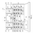
- FIG. 1illustrates a portion of semiconductor chip 10 , which may also be a portion of an un-sawed wafer (also referred to as wafer 10 ).
- Wafer 10includes substrate 12 , on which active circuits 24 are formed.
- Substrate 12may be a semiconductor substrate formed of commonly used semiconductor materials, such as silicon, silicon germanium, silicon carbide, gallium arsenide, or the like.
- Active circuits 24may include complementary metal-oxide-semiconductor (CMOS) transistors, diodes, resistors, capacitors (not shown), and/or the like.
- Interconnect structure 26is formed over active circuits 24 .
- Interconnect structure 26includes a plurality of metallization layers comprising metal lines 28 (including active metal lines 28 A and dummy metal lines 28 B) and vias 30 (including active vias 30 A and dummy vias 30 B) in a plurality of dielectric layers 32 , which include commonly known inter-metal dielectrics (IMDs).
- IMDsinter-metal dielectrics
- Metal lines 28are also commonly known as trench interconnects.
- Dielectric layers 32 in interconnect structure 26may include low-k dielectric layers, which may have k values lower than about 3.0, or even lower than about 2.5.
- Dummy metal lines 28 B and dummy vias 30 Bmay be formed in the metallization layers including the bottom metallization layer (commonly known as Ml), the top metallization layer (commonly known as M-top), and all metallization layers therebetween. Dummy metal lines 28 B and dummy vias 30 B in different metallization layers may vertically overlap each other, and connect with each other to form a tower, or may be isolated from each other. Metal lines 28 and vias 30 may be formed using damascene processes. Alternatively, they may be formed by depositing blanket metal layers, and then etching the blanket metal layers to form desirable patterns. Active metal lines 28 A and active vias 30 A have electrical functions for electrically coupling integrated circuit devices. For example, active metal lines 28 A and active vias 30 A may interconnect different devices in active circuits 24 , and may connect active circuits 24 to overlying metal pads and solder bumps.
- Metal pads 40are formed over interconnect structure 26 , and may be formed in passivation layer(s) 36 , which may be formed of silicon oxide, silicon nitride, un-doped silicate glass (USG), polyimide, or the like.
- Metal pads 40may comprise aluminum, and hence are also referred to as aluminum pads 40 throughout the description, although they may also be formed of, or include, other metallic materials, such as copper, silver, gold, nickel, tungsten, alloys thereof, and/or multi-layers thereof.
- Active metal pad 40 Amay be electrically coupled to active circuits 24 through active metal lines 28 A and active vias 30 A in interconnect structure 26 .
- metal pads 40are formed of aluminum copper (AlCu). Over metal pads 40 , under-bump-metallurgies (UBMs) 42 and metal bump 44 may be formed. In an embodiment, metal bump 44 is a solder bump. In alternative embodiments, metal bump 44 is a copper bump, and may be coated with nickel, gold, or other metals or metal alloys.
- AlCualuminum copper
- UBMsunder-bump-metallurgies
- metal bump 44is a solder bump.
- metal bump 44is a copper bump, and may be coated with nickel, gold, or other metals or metal alloys.
- Dummy metal pad 40 Bmay be formed at a same level, and formed simultaneously with, active metal pad 40 A.
- Dummy metal pad 40 B, dummy metal lines 28 B, and dummy vias 30 Bmay not have any electrical function. In other words, they may be electrically decoupled from all active circuits in wafer 10 , and may be electrically decoupled from metal bumps/metal pads on the surface of wafer 10 .
- dummy metal pad 40 B, dummy metal lines 28 B, and dummy vias 30 Bare electrically floating.
- dummy metal pad 40 BWith the formation of dummy metal pad 40 B, dummy metal lines 28 B, and dummy vias 30 B, the pattern densities in wafer 10 become more uniform, and hence the pattern-loading effect in the formation of metal lines 28 , vias 30 , and metal pads 40 is reduced.
- TSVs 20are formed in wafer 10 and extend into substrate 12 .
- TSVs 20are formed using a via-first approach, and is formed before the formation of a bottom metallization layer (commonly known as Ml). Accordingly, TSVs 20 only extend into inter-layer dielectric (ILD) 23 that is used to cover the active devices, but not into the IMD layers in interconnect structure 26 .
- ILDinter-layer dielectric
- TSVs 20are formed using a via-last approach, and are formed after the formation of interconnect structure 26 .
- TSVs 20penetrate through both substrate 12 and interconnect structure 26 , and extend into substrate 12 .
- Isolation layers 22are formed on the sidewalls of TSVs 20 and electrically insulate TSVs 20 from substrate 12 .
- Isolation layers 22may be formed of commonly used dielectric materials, such as silicon nitride, silicon oxide (for example, tetra-ethyl-ortho-silicate (TEOS) oxide), or the like.
- Active TSV 20 Amay be electrically coupled to active circuits 24 , active metal lines 28 A and active vias 28 B.
- Dummy TSV 20 Bmay be electrically coupled to, or may be decoupled from, dummy metal lines 28 B and dummy vias 28 B. Further, dummy TSV 20 B may physically contact the dummy features in interconnect structure 26 to form an integrated metal structure.
- the pattern density of TSV openings(filled with TSVs 20 ) may be more uniform than if no dummy TSV 20 B is formed, and the pattern-loading effect, for example, in the etching of substrate 12 for the formation of TSVs 20 , is reduced.
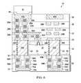
- carrier 50is bonded to the front side of wafer 10 through adhesive 52 .
- a backside grindingis performed to remove excess portions of substrate 12 so that TSVs 20 are exposed.
- Backside isolation layer 54is formed to cover back surface 12 B of substrate 12 .
- the formation of backside isolation layer 54includes slightly etching back surface 12 B of substrate 12 , blanket forming backside isolation layer 54 , and performing a light chemical mechanical polish (CMP) to remove the portion of backside isolation layer 54 directly over TSVs 20 . Accordingly, TSVs 20 are exposed through backside isolation layer 54 .
- CMPlight chemical mechanical polish
- Backside interconnect structure 60is formed on the backside of wafer 10 , and then carrier 50 is de-bonded.
- Backside interconnect structure 60may also include a plurality of metal lines 68 (including active metal lines 68 A and dummy metal lines 68 B) and vias 70 (including active vias 70 A and dummy vias 70 B) in a plurality of dielectric layers 72 .
- Dielectric layer 72may be formed of dielectric materials, such as silicon oxide, silicon nitride, polyimide, and/or the like, and may be formed using CVD, spin-on, or other commonly used methods.
- active metal lines 68 A and active vias 70 Ahave electrical functions for interconnecting integrated circuit devices, and may be electrically coupled to active TSV 20 A, active circuits 24 , active metal lines 28 A, and/or active vias 30 A.
- Dummy metal lines 68 B and dummy vias 70 Bmay not have electrical functions, and may be electrically floating. However, dummy metal lines 68 B and dummy vias 70 B may be electrically coupled to dummy TSV 20 A, dummy metal lines 28 A, and/or dummy vias 30 A, although all of them may be electrically floating.
- first dummy featurewhen referred to as being “electrically coupled” to a second dummy feature, it indicates that a conductive path may be found between the first and the second dummy features, although both of them may be floating.
- metal lines 68 and vias 70may be formed either using damascene processes, or formed by depositing and etching blanket metal layers.
- the backside interconnect structureincludes active metal pad (or bond pad) 74 A and dummy metal pad 74 B, wherein active metal pad 74 A is used for bonding the respective chip to another device, such as a die or a package substrate. Dummy metal pad 74 B, on the other hand, is not used for bonding, and may be electrically floating.
- UBM 76 and metal bump 78may be formed on active metal pad 74 A.
- wafer 10is sawed into dies, during the use of the dies, electrical signals may be connected to active circuits 24 , active metal lines 28 A/ 68 A, and active vias 30 A/ 70 A. However, no electrical signal or voltage may be connected to dummy metal lines 28 A/ 68 A and dummy vias 30 A/ 70 A.
- FIGS. 4 through 6illustrate variations of the embodiments. Like reference notations in these embodiments represent like elements as in the previously discussed embodiments, unless specified otherwise.
- the embodiment shown in FIG. 4is similar to the embodiment shown in FIG. 3 , except no dummy vias are formed in any of front-side interconnect structure 26 and backside interconnect structure 60 . However, dummy metal lines 28 B and 68 B are still formed.
- dummy vias 30 Bare formed in front-side interconnect structure 26 , while no dummy vias are formed in backside interconnect structure 60 . Accordingly, dummy metal lines 68 B are formed as discrete features electrically insulated from each other.
- FIG. 4is similar to the embodiment shown in FIG. 3 , except no dummy vias are formed in any of front-side interconnect structure 26 and backside interconnect structure 60 . However, dummy metal lines 28 B and 68 B are still formed.
- dummy vias 30 Bare formed in front-side interconnect structure 26 , while no d
- dummy TSV 20 Bmay, or may not, be formed, while active TSV 20 A is still formed.
- the formation of backside interconnect structure 60suffers less from pattern-loading effects. Further, the dummy metal lines and dummy vias on the backside of wafer 10 may be connected to the dummy metal lines and dummy vias on the front side of wafer 10 to form an integrated metal feature. As a result, the likelihood of dielectric peeling between dielectric layers 32 and 72 is reduced, and hence the strength of wafer 10 may be improved.
Landscapes
- Engineering & Computer Science (AREA)
- Computer Hardware Design (AREA)
- Microelectronics & Electronic Packaging (AREA)
- Power Engineering (AREA)
- Physics & Mathematics (AREA)
- Condensed Matter Physics & Semiconductors (AREA)
- General Physics & Mathematics (AREA)
- Manufacturing & Machinery (AREA)
- Internal Circuitry In Semiconductor Integrated Circuit Devices (AREA)
Abstract
Description
This disclosure relates generally to semiconductor devices, and more particularly to three-dimensional integrated circuits (3DICs), and even more particularly to dummy patterns formed on the backside of wafers.
The semiconductor industry has experienced continuous rapid growth due to constant improvements in the integration density of various electronic components (i.e., transistors, diodes, resistors, capacitors, etc.). For the most part, these improvements in integration density have come from repeated reductions in minimum feature size, allowing more components to be integrated into a given chip area.
These integration improvements are essentially two-dimensional (2D) in nature, in that the volume occupied by the integrated components is essentially on the surface of the semiconductor wafer. Although dramatic improvements in lithography have resulted in considerable improvements in 2D integrated circuit formations, there are physical limitations to the density that can be achieved in two dimensions. One of these limitations is the minimum size needed to make these components. Also, when more devices are put into one chip, more complex designs are required.
An additional limitation comes from the significant increase in the number and lengths of interconnections between devices as the number of devices increases. When the number and the lengths of interconnections increase, both circuit RC delay and power consumption increase.
Among the efforts for resolving the above-discussed limitations, three-dimensional integrated circuits (3DICs) and stacked dies are commonly used. Through-silicon vias (TSVs) are thus used in 3DICs and stacked dies. In this case, TSVs are often used to connect the integrated circuits on a die to the backside of the die. In addition, TSVs are also used to provide short grounding paths for grounding the integrated circuits through the backside of the die, which may be covered by a grounded metallic film.
In accordance with one aspect, a device includes a semiconductor substrate including a front side and a backside. A through-substrate via (TSV) penetrates the semiconductor substrate. A dummy metal line is formed on the backside of the semiconductor substrate, and may be connected to the TSV.
Other embodiments are also disclosed.
For a more complete understanding of the embodiments, and the advantages thereof, reference is now made to the following descriptions taken in conjunction with the accompanying drawings, in which:
The making and using of the embodiments of the disclosure are discussed in detail below. It should be appreciated, however, that the embodiments provide many applicable inventive concepts that can be embodied in a wide variety of specific contexts. The specific embodiments discussed are merely illustrative and do not limit the scope of the disclosure.
A novel integrated circuit device comprising through-substrate vias (TSVs) and the method of forming the same are provided in accordance with an embodiment. The variations of the embodiment are then discussed. Throughout the various views and illustrative embodiments, like reference numbers are used to designate like elements.
Metal pads40 (includingactive metal pad 40A anddummy metal pad 40B) are formed overinterconnect structure 26, and may be formed in passivation layer(s)36, which may be formed of silicon oxide, silicon nitride, un-doped silicate glass (USG), polyimide, or the like. Metal pads40 may comprise aluminum, and hence are also referred to as aluminum pads40 throughout the description, although they may also be formed of, or include, other metallic materials, such as copper, silver, gold, nickel, tungsten, alloys thereof, and/or multi-layers thereof.Active metal pad 40A may be electrically coupled toactive circuits 24 throughactive metal lines 28A andactive vias 30A ininterconnect structure 26. In an embodiment, metal pads40 are formed of aluminum copper (AlCu). Over metal pads40, under-bump-metallurgies (UBMs)42 andmetal bump 44 may be formed. In an embodiment,metal bump 44 is a solder bump. In alternative embodiments,metal bump 44 is a copper bump, and may be coated with nickel, gold, or other metals or metal alloys.
Through-substrate vias (TSVs)20 (including active TSV20A and dummy TSV20B) are formed inwafer 10 and extend intosubstrate 12. In a first embodiment, as shown inFIG. 1 , TSVs20 are formed using a via-first approach, and is formed before the formation of a bottom metallization layer (commonly known as Ml). Accordingly, TSVs20 only extend into inter-layer dielectric (ILD)23 that is used to cover the active devices, but not into the IMD layers ininterconnect structure 26. In alternative embodiments, TSVs20 are formed using a via-last approach, and are formed after the formation ofinterconnect structure 26. Accordingly, TSVs20 penetrate through bothsubstrate 12 andinterconnect structure 26, and extend intosubstrate 12.Isolation layers 22 are formed on the sidewalls of TSVs20 and electrically insulate TSVs20 fromsubstrate 12.Isolation layers 22 may be formed of commonly used dielectric materials, such as silicon nitride, silicon oxide (for example, tetra-ethyl-ortho-silicate (TEOS) oxide), or the like.
Referring toFIG. 2 ,carrier 50 is bonded to the front side ofwafer 10 throughadhesive 52. A backside grinding is performed to remove excess portions ofsubstrate 12 so that TSVs20 are exposed.Backside isolation layer 54 is formed to cover backsurface 12B ofsubstrate 12. In an exemplary embodiment, the formation ofbackside isolation layer 54 includes slightly etching backsurface 12B ofsubstrate 12, blanket formingbackside isolation layer 54, and performing a light chemical mechanical polish (CMP) to remove the portion ofbackside isolation layer 54 directly over TSVs20. Accordingly, TSVs20 are exposed throughbackside isolation layer 54.
Next, as shown inFIG. 3 ,backside interconnect structure 60 is formed on the backside ofwafer 10, and thencarrier 50 is de-bonded.Backside interconnect structure 60 may also include a plurality of metal lines68 (includingactive metal lines 68A anddummy metal lines 68B) and vias70 (includingactive vias 70A and dummy vias70B) in a plurality of dielectric layers72.Dielectric layer 72 may be formed of dielectric materials, such as silicon oxide, silicon nitride, polyimide, and/or the like, and may be formed using CVD, spin-on, or other commonly used methods. Again,active metal lines 68A andactive vias 70A have electrical functions for interconnecting integrated circuit devices, and may be electrically coupled toactive TSV 20A,active circuits 24,active metal lines 28A, and/oractive vias 30A.Dummy metal lines 68B and dummy vias70B may not have electrical functions, and may be electrically floating. However,dummy metal lines 68B and dummy vias70B may be electrically coupled todummy TSV 20A,dummy metal lines 28A, and/or dummy vias30A, although all of them may be electrically floating. Throughout the description, when a first dummy feature is referred to as being “electrically coupled” to a second dummy feature, it indicates that a conductive path may be found between the first and the second dummy features, although both of them may be floating. Again, metal lines68 and vias70 may be formed either using damascene processes, or formed by depositing and etching blanket metal layers. In an embodiment, the backside interconnect structure includes active metal pad (or bond pad)74A anddummy metal pad 74B, whereinactive metal pad 74A is used for bonding the respective chip to another device, such as a die or a package substrate.Dummy metal pad 74B, on the other hand, is not used for bonding, and may be electrically floating. In alternative embodiments,UBM 76 andmetal bump 78 may be formed onactive metal pad 74A.
In subsequent steps,wafer 10 is sawed into dies, during the use of the dies, electrical signals may be connected toactive circuits 24,active metal lines 28A/68A, andactive vias 30A/70A. However, no electrical signal or voltage may be connected todummy metal lines 28A/68A and dummy vias30A/70A.
With the formation of dummy metal lines and dummy vias on the backside ofwafer 10, the formation ofbackside interconnect structure 60 suffers less from pattern-loading effects. Further, the dummy metal lines and dummy vias on the backside ofwafer 10 may be connected to the dummy metal lines and dummy vias on the front side ofwafer 10 to form an integrated metal feature. As a result, the likelihood of dielectric peeling betweendielectric layers wafer 10 may be improved.
Although the embodiments and their advantages have been described in detail, it should be understood that various changes, substitutions, and alterations can be made herein without departing from the spirit and scope of the embodiments as defined by the appended claims. Moreover, the scope of the present application is not intended to be limited to the particular embodiments of the process, machine, manufacture, and composition of matter, means, methods and steps described in the specification. As one of ordinary skill in the art will readily appreciate from the disclosure, processes, machines, manufacture, compositions of matter, means, methods, or steps, presently existing or later to be developed, that perform substantially the same function or achieve substantially the same result as the corresponding embodiments described herein may be utilized according to the disclosure. Accordingly, the appended claims are intended to include within their scope such processes, machines, manufacture, compositions of matter, means, methods, or steps. In addition, each claim constitutes a separate embodiment, and the combination of various claims and embodiments are within the scope of the disclosure.
Claims (20)
1. A device comprising:
a semiconductor substrate comprising a front side and a backside;
a through-substrate via (TSV) penetrating the semiconductor substrate; and
a first dummy metal line on the backside of the semiconductor substrate.
2. The device ofclaim 1 further comprising an active circuit on the front side of the semiconductor substrate, wherein the active circuit comprises a transistor.
3. The device ofclaim 2 further comprising a dummy TSV penetrating the semiconductor substrate.
4. The device ofclaim 3 , wherein the first dummy metal line is electrically coupled to the dummy TSV, and wherein the first dummy metal line and the dummy TSV are electrically floating.
5. The device ofclaim 4 further comprising a second dummy metal line on the front side of the semiconductor substrate, wherein the second dummy metal line is electrically coupled to the dummy TSV and the first dummy metal line.
6. The device ofclaim 4 further comprising:
a plurality of dielectric layers on the backside of the semiconductor substrate;
a plurality of dummy metal lines, with one of the plurality of dummy metal lines in each of the plurality of dielectric layers; and
a plurality of dummy vias electrically coupled to the plurality of dummy metal lines, with the plurality of dummy metal lines, the plurality of dummy vias, and the dummy TSV forming an integrated metal structure.
7. The device ofclaim 1 further comprising a bond pad on the backside of the semiconductor substrate, and a dummy metal pad at a same level as the bond pad.
8. The device ofclaim 1 further comprising a dummy via on the backside of the semiconductor substrate and connected to the first dummy metal line.
9. A device comprising:
a semiconductor substrate comprising a front side and a backside;
an active circuit on the front side of the semiconductor substrate;
a through-substrate via (TSV) penetrating the semiconductor substrate;
a dummy TSV penetrating the semiconductor substrate; and
a first dummy metal line on the backside of the semiconductor substrate and electrically coupled to the dummy TSV, wherein the first dummy metal line and the dummy TSV are electrically floating.
10. The device ofclaim 9 , wherein the first dummy metal line physically contacts the dummy TSV.
11. The device ofclaim 9 , wherein the semiconductor substrate is a portion of a chip, and wherein the device further comprises:
a bond pad at a back surface of the chip; and
a dummy metal feature at a same level as the bond pad.
12. The device ofclaim 9 further comprising:
a plurality of dielectric layers on the backside of the semiconductor substrate; and
a plurality of dummy metal features, with each of the plurality of dielectric layers comprising one of the plurality of dummy metal features therein, and wherein the plurality of dummy metal features and the dummy TSV form an integrated metal structure.
13. The device ofclaim 12 further comprising a plurality of dummy vias, each in one of the plurality of dielectric layers and contacting a respective one of the plurality of dummy metal features.
14. The device ofclaim 9 further comprising a second dummy metal line on the front side of the semiconductor substrate.
15. The device ofclaim 14 , wherein the second dummy metal line is electrically coupled to the dummy TSV and the first dummy metal line.
16. The device ofclaim 14 further comprising:
a plurality of dielectric layers on the front side of the semiconductor substrate; and
a plurality of dummy metal features, with each of the plurality of dielectric layers comprising one of the plurality of dummy metal features therein, wherein the plurality of dummy metal features is electrically coupled to the dummy TSV.
17. A device comprising:
a semiconductor substrate comprising a front side and a backside;
an active circuit on the front side of the semiconductor substrate;
a through-substrate via (TSV) penetrating the semiconductor substrate;
a dummy TSV penetrating the semiconductor substrate;
a first plurality of dielectric layers on the backside of the semiconductor substrate;
a first plurality of dummy metal features, with each of the first plurality of dielectric layers comprising one of the first plurality of dummy metal features therein;
a second plurality of dielectric layers on the front side of the semiconductor substrate; and
a second plurality of dummy metal features, with each of the second plurality of dielectric layers comprising one of the second plurality of dummy metal features therein, and wherein the first and the second plurality of dummy metal features and the dummy TSV form an integrated metal structure, and are electrically floating.
18. The device ofclaim 17 further comprising a bond pad on the backside of the semiconductor substrate, wherein one of the first plurality of dummy metal features is at a same level as the bond pad.
19. The device ofclaim 17 , wherein one of the first plurality of dummy metal features is a dummy via.
20. The device ofclaim 2 , wherein the first dummy metal line is electrically floating.
Priority Applications (1)
| Application Number | Priority Date | Filing Date | Title |
|---|---|---|---|
| US12/756,727US8174124B2 (en) | 2010-04-08 | 2010-04-08 | Dummy pattern in wafer backside routing |
Applications Claiming Priority (1)
| Application Number | Priority Date | Filing Date | Title |
|---|---|---|---|
| US12/756,727US8174124B2 (en) | 2010-04-08 | 2010-04-08 | Dummy pattern in wafer backside routing |
Publications (2)
| Publication Number | Publication Date |
|---|---|
| US20110248404A1 US20110248404A1 (en) | 2011-10-13 |
| US8174124B2true US8174124B2 (en) | 2012-05-08 |
Family
ID=44760341
Family Applications (1)
| Application Number | Title | Priority Date | Filing Date |
|---|---|---|---|
| US12/756,727Active2030-08-27US8174124B2 (en) | 2010-04-08 | 2010-04-08 | Dummy pattern in wafer backside routing |
Country Status (1)
| Country | Link |
|---|---|
| US (1) | US8174124B2 (en) |
Cited By (22)
| Publication number | Priority date | Publication date | Assignee | Title |
|---|---|---|---|---|
| US20100140805A1 (en)* | 2008-12-10 | 2010-06-10 | Hung-Pin Chang | Bump Structure for Stacked Dies |
| US20100171197A1 (en)* | 2009-01-05 | 2010-07-08 | Hung-Pin Chang | Isolation Structure for Stacked Dies |
| US20110068466A1 (en)* | 2009-09-22 | 2011-03-24 | Taiwan Semiconductor Manufacturing Company, Ltd. | Wafer Backside Interconnect Structure Connected to TSVs |
| US20130140687A1 (en)* | 2011-12-06 | 2013-06-06 | Kabushiki Kaisha Toshiba | Semiconductor device |
| US8466059B2 (en) | 2010-03-30 | 2013-06-18 | Taiwan Semiconductor Manufacturing Company, Ltd. | Multi-layer interconnect structure for stacked dies |
| US20130175682A1 (en)* | 2009-10-09 | 2013-07-11 | Elpida Memory, Inc. | Semiconductor device and information processing system including the same |
| KR20140134130A (en)* | 2013-05-13 | 2014-11-21 | 에스케이하이닉스 주식회사 | Semiconductor deivce |
| US8900994B2 (en) | 2011-06-09 | 2014-12-02 | Taiwan Semiconductor Manufacturing Company, Ltd. | Method for producing a protective structure |
| US8952500B2 (en)* | 2013-03-15 | 2015-02-10 | IPEnval Consultant Inc. | Semiconductor device |
| US9184112B1 (en) | 2014-12-17 | 2015-11-10 | International Business Machines Corporation | Cooling apparatus for an integrated circuit |
| US9269607B2 (en) | 2014-06-17 | 2016-02-23 | Globalfoundries Inc. | Wafer stress control with backside patterning |
| US9472483B2 (en) | 2014-12-17 | 2016-10-18 | International Business Machines Corporation | Integrated circuit cooling apparatus |
| US9627256B2 (en)* | 2013-02-27 | 2017-04-18 | Taiwan Semiconductor Manufacturing Company, Ltd. | Integrated circuit interconnects and methods of making same |
| US9673133B2 (en) | 2014-11-12 | 2017-06-06 | Samsung Electronics Co., Ltd. | Semiconductor devices having through-electrodes |
| US10256203B2 (en)* | 2017-07-27 | 2019-04-09 | Taiwan Semiconductor Manufacturing Co., Ltd. | Semiconductor device and semiconductor package |
| US10636760B2 (en) | 2018-01-11 | 2020-04-28 | Samsung Electronics Co., Ltd. | Semiconductor packages |
| US20210358850A1 (en)* | 2020-05-15 | 2021-11-18 | Taiwan Semiconductor Manufacturing Company, Ltd. | Integrated circuit device and method |
| US20220084960A1 (en)* | 2020-09-11 | 2022-03-17 | Renesas Electronics Corporation | Semiconductor device |
| US20220173092A1 (en)* | 2014-03-28 | 2022-06-02 | Taiwan Semiconductor Manufacturing Co., Ltd. | Hybrid Bonding with Uniform Pattern Density |
| US20230299001A1 (en)* | 2022-03-21 | 2023-09-21 | Apple Inc. | Dual Contact and Power Rail for High Performance Standard Cells |
| US11996402B2 (en) | 2020-11-02 | 2024-05-28 | Samsung Electronics Co., Ltd. | Semiconductor device |
| US12068270B2 (en) | 2020-05-27 | 2024-08-20 | Samsung Electronics Co., Ltd. | Semiconductor package |
Families Citing this family (31)
| Publication number | Priority date | Publication date | Assignee | Title |
|---|---|---|---|---|
| US7928534B2 (en) | 2008-10-09 | 2011-04-19 | Taiwan Semiconductor Manufacturing Company, Ltd. | Bond pad connection to redistribution lines having tapered profiles |
| US8736050B2 (en) | 2009-09-03 | 2014-05-27 | Taiwan Semiconductor Manufacturing Company, Ltd. | Front side copper post joint structure for temporary bond in TSV application |
| US8759949B2 (en)* | 2009-04-30 | 2014-06-24 | Taiwan Semiconductor Manufacturing Company, Ltd. | Wafer backside structures having copper pillars |
| US8193639B2 (en)* | 2010-03-30 | 2012-06-05 | Taiwan Semiconductor Manufacturing Company, Ltd. | Dummy metal design for packaging structures |
| US8269316B2 (en)* | 2010-07-07 | 2012-09-18 | Victory Gain Group Corporation | Silicon based substrate and manufacturing method thereof |
| US8581389B2 (en)* | 2011-05-27 | 2013-11-12 | Taiwan Semiconductor Manufacturing Company, Ltd. | Uniformity control for IC passivation structure |
| US8618647B2 (en)* | 2011-08-01 | 2013-12-31 | Tessera, Inc. | Packaged microelectronic elements having blind vias for heat dissipation |
| US8912649B2 (en)* | 2011-08-17 | 2014-12-16 | Taiwan Semiconductor Manufacturing Company, Ltd. | Dummy flip chip bumps for reducing stress |
| CN103456716B (en)* | 2012-05-29 | 2016-05-11 | 旺宏电子股份有限公司 | Three-dimensional multi-chip laminated module and manufacturing method thereof |
| US9412661B2 (en)* | 2012-11-21 | 2016-08-09 | Taiwan Semiconductor Manufacturing Company, Ltd. | Method for forming package-on-package structure |
| US8933564B2 (en)* | 2012-12-21 | 2015-01-13 | Intel Corporation | Landing structure for through-silicon via |
| US9082761B2 (en)* | 2013-06-01 | 2015-07-14 | Taiwan Semiconductor Manufacturing Company, Ltd. | Polymer layers embedded with metal pads for heat dissipation |
| US9331062B1 (en)* | 2013-12-06 | 2016-05-03 | Altera Corporation | Integrated circuits with backside power delivery |
| US9236326B2 (en) | 2014-04-25 | 2016-01-12 | Taiwan Semiconductor Manufacturing Co., Ltd. | Semiconductor structure and fabricating method thereof |
| US9620454B2 (en)* | 2014-09-12 | 2017-04-11 | Qualcomm Incorporated | Middle-of-line (MOL) manufactured integrated circuits (ICs) employing local interconnects of metal lines using an elongated via, and related methods |
| US9972581B1 (en) | 2017-02-07 | 2018-05-15 | Taiwan Semiconductor Manufacturing Company, Ltd. | Routing design of dummy metal cap and redistribution line |
| US10157867B1 (en) | 2017-08-31 | 2018-12-18 | Taiwan Semiconductor Manufacturing Company, Ltd. | Interconnect structure and method |
| US11069630B2 (en)* | 2018-09-21 | 2021-07-20 | Taiwan Semiconductor Manufacturing Co., Ltd. | Structures and methods for reducing thermal expansion mismatch during integrated circuit packaging |
| US12131976B2 (en)* | 2018-09-21 | 2024-10-29 | United Microelectronics Corp. | Semiconductor structure with heat dissipation structure and method of fabricating the same |
| US10861808B2 (en)* | 2018-11-21 | 2020-12-08 | Taiwan Semiconductor Manufacturing Company, Ltd. | Bonding structure of dies with dangling bonds |
| KR102849028B1 (en)* | 2019-02-28 | 2025-08-22 | 소니 세미컨덕터 솔루션즈 가부시키가이샤 | imaging sensor |
| US11437283B2 (en) | 2019-03-15 | 2022-09-06 | Intel Corporation | Backside contacts for semiconductor devices |
| US10998293B2 (en)* | 2019-06-14 | 2021-05-04 | Taiwan Semiconductor Manufacturing Company, Ltd. | Method of fabricating semiconductor structure |
| TWI755861B (en)* | 2020-09-18 | 2022-02-21 | 財團法人工業技術研究院 | Redistribution structure and forming method thereof |
| US12170273B2 (en)* | 2020-12-01 | 2024-12-17 | Intel Corporation | Integrated circuit assemblies with direct chip attach to circuit boards |
| WO2022141427A1 (en)* | 2020-12-31 | 2022-07-07 | 华为技术有限公司 | Chip, chip packaging structure, and electronic device |
| KR20220111089A (en)* | 2021-02-01 | 2022-08-09 | 삼성전자주식회사 | Semiconductor package |
| US20220352018A1 (en)* | 2021-04-30 | 2022-11-03 | Taiwan Semiconductor Manufacturing Company, Ltd. | Carbon-based liner to reduce contact resistance |
| US12341094B2 (en)* | 2021-05-19 | 2025-06-24 | Changxin Memory Technologies, Inc. | Semiconductor structure |
| US12261109B2 (en) | 2021-05-19 | 2025-03-25 | Changxin Memory Technologies, Inc. | Semiconductor structure |
| US20220415807A1 (en)* | 2021-06-25 | 2022-12-29 | Intel Corporation | Thermal management structures in semiconductor devices and methods of fabrication |
Citations (53)
| Publication number | Priority date | Publication date | Assignee | Title |
|---|---|---|---|---|
| US3461357A (en) | 1967-09-15 | 1969-08-12 | Ibm | Multilevel terminal metallurgy for semiconductor devices |
| US5391917A (en) | 1993-05-10 | 1995-02-21 | International Business Machines Corporation | Multiprocessor module packaging |
| US5510298A (en) | 1991-09-12 | 1996-04-23 | Texas Instruments Incorporated | Method of interconnect in an integrated circuit |
| US5767001A (en) | 1993-05-05 | 1998-06-16 | Siemens Aktiengesellschaft | Process for producing semiconductor components between which contact is made vertically |
| US5897362A (en) | 1998-04-17 | 1999-04-27 | Lucent Technologies Inc. | Bonding silicon wafers |
| US5998292A (en) | 1997-11-12 | 1999-12-07 | International Business Machines Corporation | Method for making three dimensional circuit integration |
| US6184060B1 (en) | 1996-10-29 | 2001-02-06 | Trusi Technologies Llc | Integrated circuits and methods for their fabrication |
| US6322903B1 (en) | 1999-12-06 | 2001-11-27 | Tru-Si Technologies, Inc. | Package of integrated circuits and vertical integration |
| US6376332B1 (en) | 1999-02-02 | 2002-04-23 | Canon Kabushiki Kaisha | Composite member and separating method therefor, bonded substrate stack and separating method therefor, transfer method for transfer layer, and SOI substrate manufacturing method |
| US6448168B1 (en) | 1997-09-30 | 2002-09-10 | Intel Corporation | Method for distributing a clock on the silicon backside of an integrated circuit |
| US6465892B1 (en) | 1999-04-13 | 2002-10-15 | Oki Electric Industry Co., Ltd. | Interconnect structure for stacked semiconductor device |
| US6538333B2 (en) | 2000-06-16 | 2003-03-25 | Chartered Semiconductor Manufacturing Ltd. | Three dimensional IC package module |
| US6599778B2 (en) | 2001-12-19 | 2003-07-29 | International Business Machines Corporation | Chip and wafer integration process using vertical connections |
| US6664129B2 (en) | 1996-10-29 | 2003-12-16 | Tri-Si Technologies, Inc. | Integrated circuits and methods for their fabrication |
| US20040151917A1 (en) | 2003-01-31 | 2004-08-05 | Taiwan Semiconductor Manufacturing Company | Bonded soi wafer with <100> device layer and <110> substrate for performance improvement |
| US6800930B2 (en) | 2002-07-31 | 2004-10-05 | Micron Technology, Inc. | Semiconductor dice having back side redistribution layer accessed using through-silicon vias, and assemblies |
| US6841883B1 (en) | 2003-03-31 | 2005-01-11 | Micron Technology, Inc. | Multi-dice chip scale semiconductor components and wafer level methods of fabrication |
| US6897125B2 (en) | 2003-09-17 | 2005-05-24 | Intel Corporation | Methods of forming backside connections on a wafer stack |
| US6924551B2 (en) | 2003-05-28 | 2005-08-02 | Intel Corporation | Through silicon via, folded flex microelectronic package |
| US20050236693A1 (en) | 2004-04-15 | 2005-10-27 | Werner Kroninger | Wafer stabilization device and associated production method |
| US6962872B2 (en) | 2002-12-09 | 2005-11-08 | International Business Machines Corporation | High density chip carrier with integrated passive devices |
| US20060046431A1 (en) | 2004-08-26 | 2006-03-02 | Siltronic Ag | Layered semiconductor wafer with low warp and bow, and process for producing it |
| US20060099791A1 (en) | 2001-12-04 | 2006-05-11 | Shin-Etsu Handotai Co., Ltd. | Bonded wafer and method of producing bonded wafer |
| US7049170B2 (en) | 2003-12-17 | 2006-05-23 | Tru-Si Technologies, Inc. | Integrated circuits and packaging substrates with cavities, and attachment methods including insertion of protruding contact pads into cavities |
| US7060601B2 (en) | 2003-12-17 | 2006-06-13 | Tru-Si Technologies, Inc. | Packaging substrates for integrated circuits and soldering methods |
| US7071546B2 (en) | 2002-01-16 | 2006-07-04 | Alfred E. Mann Foundation For Scientific Research | Space-saving packaging of electronic circuits |
| US7111149B2 (en) | 2003-07-07 | 2006-09-19 | Intel Corporation | Method and apparatus for generating a device ID for stacked devices |
| US7122912B2 (en) | 2004-01-28 | 2006-10-17 | Nec Electronics Corporation | Chip and multi-chip semiconductor device using thereof and method for manufacturing same |
| US7157787B2 (en) | 2002-02-20 | 2007-01-02 | Intel Corporation | Process of vertically stacking multiple wafers supporting different active integrated circuit (IC) devices |
| US7193308B2 (en) | 2003-09-26 | 2007-03-20 | Seiko Epson Corporation | Intermediate chip module, semiconductor device, circuit board, and electronic device |
| US7262495B2 (en) | 2004-10-07 | 2007-08-28 | Hewlett-Packard Development Company, L.P. | 3D interconnect with protruding contacts |
| US20070210259A1 (en) | 2006-03-08 | 2007-09-13 | Kerwin David B | Cross-talk and back side shielding in a front side illuminated photo detector diode array |
| US7291542B2 (en) | 2002-09-30 | 2007-11-06 | Renesas Technology Corp. | Semiconductor wafer and manufacturing method thereof |
| US7297574B2 (en) | 2005-06-17 | 2007-11-20 | Infineon Technologies Ag | Multi-chip device and method for producing a multi-chip device |
| US20080035854A1 (en) | 2004-07-12 | 2008-02-14 | The Regents Of The University Of California | Electron Microscope Phase Enhancement |
| US7335972B2 (en) | 2003-11-13 | 2008-02-26 | Sandia Corporation | Heterogeneously integrated microsystem-on-a-chip |
| US20080057678A1 (en) | 2006-08-31 | 2008-03-06 | Kishor Purushottam Gadkaree | Semiconductor on glass insulator made using improved hydrogen reduction process |
| US20080079121A1 (en) | 2006-09-30 | 2008-04-03 | Kwon Whan Han | Through-silicon via and method for forming the same |
| US7371663B2 (en) | 2005-07-06 | 2008-05-13 | Taiwan Semiconductor Manufacturing Co., Ltd. | Three dimensional IC device and alignment methods of IC device substrates |
| US20080131679A1 (en) | 2006-12-01 | 2008-06-05 | Siltronic Ag | Silicon Wafer And Method For Manufacturing The Same |
| US20090140381A1 (en) | 2007-11-29 | 2009-06-04 | Stats Chippac, Ltd. | Semiconductor Device and Method for Forming Passive Circuit Elements with Through Silicon Vias to Backside Interconnect Structures |
| US20100013102A1 (en) | 2008-07-15 | 2010-01-21 | Stats Chippac, Ltd. | Semiconductor Device and Method of Providing a Thermal Dissipation Path Through RDL and Conductive Via |
| US20100022034A1 (en) | 2008-07-22 | 2010-01-28 | Joze Eura Antol | Manufacture of devices including solder bumps |
| US20100090318A1 (en) | 2008-10-09 | 2010-04-15 | Kuo-Ching Hsu | Backside Connection to TSVs Having Redistribution Lines |
| US20100090319A1 (en) | 2008-10-09 | 2010-04-15 | Kuo-Ching Hsu | Bond Pad Connection to Redistribution Lines Having Tapered Profiles |
| US7786584B2 (en)* | 2007-11-26 | 2010-08-31 | Infineon Technologies Ag | Through substrate via semiconductor components |
| US20100276787A1 (en) | 2009-04-30 | 2010-11-04 | Taiwan Semiconductor Manufacturing Company, Ltd. | Wafer Backside Structures Having Copper Pillars |
| US7838337B2 (en)* | 2008-12-01 | 2010-11-23 | Stats Chippac, Ltd. | Semiconductor device and method of forming an interposer package with through silicon vias |
| US20100330798A1 (en) | 2009-06-26 | 2010-12-30 | Taiwan Semiconductor Manufacturing Company, Ltd. | Formation of TSV Backside Interconnects by Modifying Carrier Wafers |
| US20110049706A1 (en) | 2009-09-03 | 2011-03-03 | Taiwan Semiconductor Manufacturing Company, Ltd. | Front Side Copper Post Joint Structure for Temporary Bond in TSV Application |
| US20110186990A1 (en)* | 2010-01-29 | 2011-08-04 | Texas Instruments Incorporated | Protruding tsv tips for enhanced heat dissipation for ic devices |
| US20110193235A1 (en)* | 2010-02-05 | 2011-08-11 | Taiwan Semiconductor Manufacturing Company, Ltd. | 3DIC Architecture with Die Inside Interposer |
| US20110233785A1 (en)* | 2010-03-24 | 2011-09-29 | International Business Machines Corporation | Backside dummy plugs for 3d integration |
- 2010
- 2010-04-08USUS12/756,727patent/US8174124B2/enactiveActive
Patent Citations (62)
| Publication number | Priority date | Publication date | Assignee | Title |
|---|---|---|---|---|
| US3461357A (en) | 1967-09-15 | 1969-08-12 | Ibm | Multilevel terminal metallurgy for semiconductor devices |
| US5510298A (en) | 1991-09-12 | 1996-04-23 | Texas Instruments Incorporated | Method of interconnect in an integrated circuit |
| US5767001A (en) | 1993-05-05 | 1998-06-16 | Siemens Aktiengesellschaft | Process for producing semiconductor components between which contact is made vertically |
| US5391917A (en) | 1993-05-10 | 1995-02-21 | International Business Machines Corporation | Multiprocessor module packaging |
| US6184060B1 (en) | 1996-10-29 | 2001-02-06 | Trusi Technologies Llc | Integrated circuits and methods for their fabrication |
| US6664129B2 (en) | 1996-10-29 | 2003-12-16 | Tri-Si Technologies, Inc. | Integrated circuits and methods for their fabrication |
| US6882030B2 (en) | 1996-10-29 | 2005-04-19 | Tru-Si Technologies, Inc. | Integrated circuit structures with a conductor formed in a through hole in a semiconductor substrate and protruding from a surface of the substrate |
| US6740582B2 (en) | 1996-10-29 | 2004-05-25 | Tru-Si Technologies, Inc. | Integrated circuits and methods for their fabrication |
| US6639303B2 (en) | 1996-10-29 | 2003-10-28 | Tru-Si Technolgies, Inc. | Integrated circuits and methods for their fabrication |
| US6448168B1 (en) | 1997-09-30 | 2002-09-10 | Intel Corporation | Method for distributing a clock on the silicon backside of an integrated circuit |
| US5998292A (en) | 1997-11-12 | 1999-12-07 | International Business Machines Corporation | Method for making three dimensional circuit integration |
| US5897362A (en) | 1998-04-17 | 1999-04-27 | Lucent Technologies Inc. | Bonding silicon wafers |
| US6376332B1 (en) | 1999-02-02 | 2002-04-23 | Canon Kabushiki Kaisha | Composite member and separating method therefor, bonded substrate stack and separating method therefor, transfer method for transfer layer, and SOI substrate manufacturing method |
| US6465892B1 (en) | 1999-04-13 | 2002-10-15 | Oki Electric Industry Co., Ltd. | Interconnect structure for stacked semiconductor device |
| US6472293B2 (en) | 1999-04-13 | 2002-10-29 | Oki Electric Industry Co., Ltd. | Method for manufacturing an interconnect structure for stacked semiconductor device |
| US6693361B1 (en) | 1999-12-06 | 2004-02-17 | Tru-Si Technologies, Inc. | Packaging of integrated circuits and vertical integration |
| US6322903B1 (en) | 1999-12-06 | 2001-11-27 | Tru-Si Technologies, Inc. | Package of integrated circuits and vertical integration |
| US6538333B2 (en) | 2000-06-16 | 2003-03-25 | Chartered Semiconductor Manufacturing Ltd. | Three dimensional IC package module |
| US20060099791A1 (en) | 2001-12-04 | 2006-05-11 | Shin-Etsu Handotai Co., Ltd. | Bonded wafer and method of producing bonded wafer |
| US6599778B2 (en) | 2001-12-19 | 2003-07-29 | International Business Machines Corporation | Chip and wafer integration process using vertical connections |
| US7071546B2 (en) | 2002-01-16 | 2006-07-04 | Alfred E. Mann Foundation For Scientific Research | Space-saving packaging of electronic circuits |
| US7157787B2 (en) | 2002-02-20 | 2007-01-02 | Intel Corporation | Process of vertically stacking multiple wafers supporting different active integrated circuit (IC) devices |
| US6962867B2 (en) | 2002-07-31 | 2005-11-08 | Microntechnology, Inc. | Methods of fabrication of semiconductor dice having back side redistribution layer accessed using through-silicon vias and assemblies thereof |
| US6800930B2 (en) | 2002-07-31 | 2004-10-05 | Micron Technology, Inc. | Semiconductor dice having back side redistribution layer accessed using through-silicon vias, and assemblies |
| US7355273B2 (en) | 2002-07-31 | 2008-04-08 | Micron Technology, Inc. | Semiconductor dice having back side redistribution layer accessed using through-silicon vias, methods |
| US7291542B2 (en) | 2002-09-30 | 2007-11-06 | Renesas Technology Corp. | Semiconductor wafer and manufacturing method thereof |
| US7030481B2 (en) | 2002-12-09 | 2006-04-18 | Internation Business Machines Corporation | High density chip carrier with integrated passive devices |
| US6962872B2 (en) | 2002-12-09 | 2005-11-08 | International Business Machines Corporation | High density chip carrier with integrated passive devices |
| US20040151917A1 (en) | 2003-01-31 | 2004-08-05 | Taiwan Semiconductor Manufacturing Company | Bonded soi wafer with <100> device layer and <110> substrate for performance improvement |
| US6841883B1 (en) | 2003-03-31 | 2005-01-11 | Micron Technology, Inc. | Multi-dice chip scale semiconductor components and wafer level methods of fabrication |
| US6924551B2 (en) | 2003-05-28 | 2005-08-02 | Intel Corporation | Through silicon via, folded flex microelectronic package |
| US7111149B2 (en) | 2003-07-07 | 2006-09-19 | Intel Corporation | Method and apparatus for generating a device ID for stacked devices |
| US6897125B2 (en) | 2003-09-17 | 2005-05-24 | Intel Corporation | Methods of forming backside connections on a wafer stack |
| US7193308B2 (en) | 2003-09-26 | 2007-03-20 | Seiko Epson Corporation | Intermediate chip module, semiconductor device, circuit board, and electronic device |
| US7335972B2 (en) | 2003-11-13 | 2008-02-26 | Sandia Corporation | Heterogeneously integrated microsystem-on-a-chip |
| US7049170B2 (en) | 2003-12-17 | 2006-05-23 | Tru-Si Technologies, Inc. | Integrated circuits and packaging substrates with cavities, and attachment methods including insertion of protruding contact pads into cavities |
| US7060601B2 (en) | 2003-12-17 | 2006-06-13 | Tru-Si Technologies, Inc. | Packaging substrates for integrated circuits and soldering methods |
| US7122912B2 (en) | 2004-01-28 | 2006-10-17 | Nec Electronics Corporation | Chip and multi-chip semiconductor device using thereof and method for manufacturing same |
| US20050236693A1 (en) | 2004-04-15 | 2005-10-27 | Werner Kroninger | Wafer stabilization device and associated production method |
| US20080035854A1 (en) | 2004-07-12 | 2008-02-14 | The Regents Of The University Of California | Electron Microscope Phase Enhancement |
| US20060046431A1 (en) | 2004-08-26 | 2006-03-02 | Siltronic Ag | Layered semiconductor wafer with low warp and bow, and process for producing it |
| US7262495B2 (en) | 2004-10-07 | 2007-08-28 | Hewlett-Packard Development Company, L.P. | 3D interconnect with protruding contacts |
| US7297574B2 (en) | 2005-06-17 | 2007-11-20 | Infineon Technologies Ag | Multi-chip device and method for producing a multi-chip device |
| US7371663B2 (en) | 2005-07-06 | 2008-05-13 | Taiwan Semiconductor Manufacturing Co., Ltd. | Three dimensional IC device and alignment methods of IC device substrates |
| US20070210259A1 (en) | 2006-03-08 | 2007-09-13 | Kerwin David B | Cross-talk and back side shielding in a front side illuminated photo detector diode array |
| US20080057678A1 (en) | 2006-08-31 | 2008-03-06 | Kishor Purushottam Gadkaree | Semiconductor on glass insulator made using improved hydrogen reduction process |
| US20080079121A1 (en) | 2006-09-30 | 2008-04-03 | Kwon Whan Han | Through-silicon via and method for forming the same |
| US20080131679A1 (en) | 2006-12-01 | 2008-06-05 | Siltronic Ag | Silicon Wafer And Method For Manufacturing The Same |
| US7786584B2 (en)* | 2007-11-26 | 2010-08-31 | Infineon Technologies Ag | Through substrate via semiconductor components |
| US20090140381A1 (en) | 2007-11-29 | 2009-06-04 | Stats Chippac, Ltd. | Semiconductor Device and Method for Forming Passive Circuit Elements with Through Silicon Vias to Backside Interconnect Structures |
| US20100013102A1 (en) | 2008-07-15 | 2010-01-21 | Stats Chippac, Ltd. | Semiconductor Device and Method of Providing a Thermal Dissipation Path Through RDL and Conductive Via |
| US20100022034A1 (en) | 2008-07-22 | 2010-01-28 | Joze Eura Antol | Manufacture of devices including solder bumps |
| US20100090318A1 (en) | 2008-10-09 | 2010-04-15 | Kuo-Ching Hsu | Backside Connection to TSVs Having Redistribution Lines |
| US20100090319A1 (en) | 2008-10-09 | 2010-04-15 | Kuo-Ching Hsu | Bond Pad Connection to Redistribution Lines Having Tapered Profiles |
| US20110165776A1 (en) | 2008-10-09 | 2011-07-07 | Taiwan Semiconductor Manufacturing Company, Ltd. | Bond Pad Connection to Redistribution Lines Having Tapered Profiles |
| US7838337B2 (en)* | 2008-12-01 | 2010-11-23 | Stats Chippac, Ltd. | Semiconductor device and method of forming an interposer package with through silicon vias |
| US20100276787A1 (en) | 2009-04-30 | 2010-11-04 | Taiwan Semiconductor Manufacturing Company, Ltd. | Wafer Backside Structures Having Copper Pillars |
| US20100330798A1 (en) | 2009-06-26 | 2010-12-30 | Taiwan Semiconductor Manufacturing Company, Ltd. | Formation of TSV Backside Interconnects by Modifying Carrier Wafers |
| US20110049706A1 (en) | 2009-09-03 | 2011-03-03 | Taiwan Semiconductor Manufacturing Company, Ltd. | Front Side Copper Post Joint Structure for Temporary Bond in TSV Application |
| US20110186990A1 (en)* | 2010-01-29 | 2011-08-04 | Texas Instruments Incorporated | Protruding tsv tips for enhanced heat dissipation for ic devices |
| US20110193235A1 (en)* | 2010-02-05 | 2011-08-11 | Taiwan Semiconductor Manufacturing Company, Ltd. | 3DIC Architecture with Die Inside Interposer |
| US20110233785A1 (en)* | 2010-03-24 | 2011-09-29 | International Business Machines Corporation | Backside dummy plugs for 3d integration |
Non-Patent Citations (1)
| Title |
|---|
| Shen, L-C, et al., "A Clamped Through Silicon Via (TSV) Interconnection for Stacked Chip Bonding Using Metal Cap on Pad and Metal Column Forming in Via," 2008, IEEE, pp. 544-549. |
Cited By (42)
| Publication number | Priority date | Publication date | Assignee | Title |
|---|---|---|---|---|
| US8513119B2 (en) | 2008-12-10 | 2013-08-20 | Taiwan Semiconductor Manufacturing Company, Ltd. | Method of forming bump structure having tapered sidewalls for stacked dies |
| US20100140805A1 (en)* | 2008-12-10 | 2010-06-10 | Hung-Pin Chang | Bump Structure for Stacked Dies |
| US9312225B2 (en) | 2008-12-10 | 2016-04-12 | Taiwan Semiconductor Manufacturing Company, Ltd. | Bump structure for stacked dies |
| US20100171197A1 (en)* | 2009-01-05 | 2010-07-08 | Hung-Pin Chang | Isolation Structure for Stacked Dies |
| US10163756B2 (en) | 2009-01-05 | 2018-12-25 | Taiwan Semiconductor Manufacturing Company, Ltd. | Isolation structure for stacked dies |
| US9449875B2 (en) | 2009-09-22 | 2016-09-20 | Taiwan Semiconductor Manufacturing Company, Ltd. | Wafer backside interconnect structure connected to TSVs |
| US9978708B2 (en) | 2009-09-22 | 2018-05-22 | Taiwan Semiconductor Manufacturing Company, Ltd. | Wafer backside interconnect structure connected to TSVs |
| US8791549B2 (en)* | 2009-09-22 | 2014-07-29 | Taiwan Semiconductor Manufacturing Company, Ltd. | Wafer backside interconnect structure connected to TSVs |
| US9716074B2 (en) | 2009-09-22 | 2017-07-25 | Taiwan Semiconductor Manufacturing Company, Ltd. | Wafer backside interconnect structure connected to TSVs |
| US20110068466A1 (en)* | 2009-09-22 | 2011-03-24 | Taiwan Semiconductor Manufacturing Company, Ltd. | Wafer Backside Interconnect Structure Connected to TSVs |
| US20130175682A1 (en)* | 2009-10-09 | 2013-07-11 | Elpida Memory, Inc. | Semiconductor device and information processing system including the same |
| US8604621B2 (en)* | 2009-10-09 | 2013-12-10 | Elpida Memory, Inc. | Semiconductor device and information processing system including the same |
| US8735288B2 (en)* | 2009-10-09 | 2014-05-27 | Elpida Memory, Inc. | Semiconductor device and information processing system including the same |
| US8841773B2 (en) | 2010-03-30 | 2014-09-23 | Taiwan Semiconductor Manufacturing Company, Ltd. | Multi-layer interconnect structure for stacked dies |
| US8466059B2 (en) | 2010-03-30 | 2013-06-18 | Taiwan Semiconductor Manufacturing Company, Ltd. | Multi-layer interconnect structure for stacked dies |
| US9299676B2 (en) | 2011-06-09 | 2016-03-29 | Taiwan Semiconductor Manufacturing Company, Ltd. | Through silicon via structure |
| US8952506B2 (en) | 2011-06-09 | 2015-02-10 | Taiwan Semiconductor Manufacturing Company, Ltd. | Through silicon via structure |
| US8900994B2 (en) | 2011-06-09 | 2014-12-02 | Taiwan Semiconductor Manufacturing Company, Ltd. | Method for producing a protective structure |
| US9997497B2 (en) | 2011-06-09 | 2018-06-12 | Taiwan Semiconductor Manufacturing Company, Ltd. | Through silicon via structure |
| US9633900B2 (en) | 2011-06-09 | 2017-04-25 | Taiwan Semiconductor Manufacturing Company, Ltd. | Method for through silicon via structure |
| US20130140687A1 (en)* | 2011-12-06 | 2013-06-06 | Kabushiki Kaisha Toshiba | Semiconductor device |
| US8558390B2 (en)* | 2011-12-06 | 2013-10-15 | Kabushiki Kaisha Toshiba | Semiconductor device |
| US9627256B2 (en)* | 2013-02-27 | 2017-04-18 | Taiwan Semiconductor Manufacturing Company, Ltd. | Integrated circuit interconnects and methods of making same |
| US8952500B2 (en)* | 2013-03-15 | 2015-02-10 | IPEnval Consultant Inc. | Semiconductor device |
| KR20140134130A (en)* | 2013-05-13 | 2014-11-21 | 에스케이하이닉스 주식회사 | Semiconductor deivce |
| US20220173092A1 (en)* | 2014-03-28 | 2022-06-02 | Taiwan Semiconductor Manufacturing Co., Ltd. | Hybrid Bonding with Uniform Pattern Density |
| US12424605B2 (en) | 2014-03-28 | 2025-09-23 | Taiwan Semiconductor Manufacturing Company, Ltd. | Hybrid bonding with uniform pattern density |
| US11996399B2 (en)* | 2014-03-28 | 2024-05-28 | Taiwan Semiconductor Manufacturing Company, Ltd. | Hybrid bonding with uniform pattern density |
| US9269607B2 (en) | 2014-06-17 | 2016-02-23 | Globalfoundries Inc. | Wafer stress control with backside patterning |
| US9673133B2 (en) | 2014-11-12 | 2017-06-06 | Samsung Electronics Co., Ltd. | Semiconductor devices having through-electrodes |
| US9472483B2 (en) | 2014-12-17 | 2016-10-18 | International Business Machines Corporation | Integrated circuit cooling apparatus |
| US9184112B1 (en) | 2014-12-17 | 2015-11-10 | International Business Machines Corporation | Cooling apparatus for an integrated circuit |
| US10256203B2 (en)* | 2017-07-27 | 2019-04-09 | Taiwan Semiconductor Manufacturing Co., Ltd. | Semiconductor device and semiconductor package |
| US10636760B2 (en) | 2018-01-11 | 2020-04-28 | Samsung Electronics Co., Ltd. | Semiconductor packages |
| US12021033B2 (en)* | 2020-05-15 | 2024-06-25 | Taiwan Semiconductor Manufacturing Ltd. | Integrated circuit device having active region coupled to metal layers on opposite sides of substrate, and method |
| US20210358850A1 (en)* | 2020-05-15 | 2021-11-18 | Taiwan Semiconductor Manufacturing Company, Ltd. | Integrated circuit device and method |
| US12068270B2 (en) | 2020-05-27 | 2024-08-20 | Samsung Electronics Co., Ltd. | Semiconductor package |
| US12062627B2 (en)* | 2020-09-11 | 2024-08-13 | Renesas Electronics Corporation | Semiconductor device |
| US20240363557A1 (en)* | 2020-09-11 | 2024-10-31 | Renesas Electronics Corporation | Semiconductor device |
| US20220084960A1 (en)* | 2020-09-11 | 2022-03-17 | Renesas Electronics Corporation | Semiconductor device |
| US11996402B2 (en) | 2020-11-02 | 2024-05-28 | Samsung Electronics Co., Ltd. | Semiconductor device |
| US20230299001A1 (en)* | 2022-03-21 | 2023-09-21 | Apple Inc. | Dual Contact and Power Rail for High Performance Standard Cells |
Also Published As
| Publication number | Publication date |
|---|---|
| US20110248404A1 (en) | 2011-10-13 |
Similar Documents
| Publication | Publication Date | Title |
|---|---|---|
| US8174124B2 (en) | Dummy pattern in wafer backside routing | |
| US12387996B2 (en) | Through-substrate vias with improved connections | |
| US12362282B2 (en) | Semiconductor structure and manufacturing method thereof | |
| US20230207530A1 (en) | Stacked Semiconductor Structure and Method | |
| US11094613B2 (en) | Semiconductor structure and manufacturing method thereof | |
| US9978708B2 (en) | Wafer backside interconnect structure connected to TSVs | |
| US11682583B2 (en) | Through-vias and methods of forming the same | |
| US8158456B2 (en) | Method of forming stacked dies | |
| US8168529B2 (en) | Forming seal ring in an integrated circuit die | |
| JP5345077B2 (en) | Through-silicon via with low-k dielectric liner | |
| US10566229B2 (en) | Microelectronic package structures including redistribution layers | |
| US20250157889A1 (en) | Forming Multiple TSVs with Different Formation Schemes | |
| US20250022825A1 (en) | Seal ring structure and method of forming same |
Legal Events
| Date | Code | Title | Description |
|---|---|---|---|
| AS | Assignment | Owner name:TAIWAN SEMICONDUCTOR MANUFACTURING COMPANY, LTD., Free format text:ASSIGNMENT OF ASSIGNORS INTEREST;ASSIGNORS:CHIU, MING-YEN;CHEN, HSIEN-WEI;CHEN, MING-FA;AND OTHERS;REEL/FRAME:024217/0318 Effective date:20100330 | |
| STCF | Information on status: patent grant | Free format text:PATENTED CASE | |
| FPAY | Fee payment | Year of fee payment:4 | |
| MAFP | Maintenance fee payment | Free format text:PAYMENT OF MAINTENANCE FEE, 8TH YEAR, LARGE ENTITY (ORIGINAL EVENT CODE: M1552); ENTITY STATUS OF PATENT OWNER: LARGE ENTITY Year of fee payment:8 | |
| MAFP | Maintenance fee payment | Free format text:PAYMENT OF MAINTENANCE FEE, 12TH YEAR, LARGE ENTITY (ORIGINAL EVENT CODE: M1553); ENTITY STATUS OF PATENT OWNER: LARGE ENTITY Year of fee payment:12 |