US8173446B2 - Method of producing an integrated micromagnet sensor assembly - Google Patents
Method of producing an integrated micromagnet sensor assemblyDownload PDFInfo
- Publication number
- US8173446B2 US8173446B2US12/642,968US64296809AUS8173446B2US 8173446 B2US8173446 B2US 8173446B2US 64296809 AUS64296809 AUS 64296809AUS 8173446 B2US8173446 B2US 8173446B2
- Authority
- US
- United States
- Prior art keywords
- bias magnet
- hardened
- mask
- semiconductor material
- metal material
- Prior art date
- Legal status (The legal status is an assumption and is not a legal conclusion. Google has not performed a legal analysis and makes no representation as to the accuracy of the status listed.)
- Active, expires
Links
Images


Classifications
- B—PERFORMING OPERATIONS; TRANSPORTING
- B82—NANOTECHNOLOGY
- B82Y—SPECIFIC USES OR APPLICATIONS OF NANOSTRUCTURES; MEASUREMENT OR ANALYSIS OF NANOSTRUCTURES; MANUFACTURE OR TREATMENT OF NANOSTRUCTURES
- B82Y25/00—Nanomagnetism, e.g. magnetoimpedance, anisotropic magnetoresistance, giant magnetoresistance or tunneling magnetoresistance
- G—PHYSICS
- G01—MEASURING; TESTING
- G01R—MEASURING ELECTRIC VARIABLES; MEASURING MAGNETIC VARIABLES
- G01R33/00—Arrangements or instruments for measuring magnetic variables
- G01R33/02—Measuring direction or magnitude of magnetic fields or magnetic flux
- G01R33/06—Measuring direction or magnitude of magnetic fields or magnetic flux using galvano-magnetic devices
- G01R33/09—Magnetoresistive devices
- G01R33/093—Magnetoresistive devices using multilayer structures, e.g. giant magnetoresistance sensors
- G—PHYSICS
- G01—MEASURING; TESTING
- G01R—MEASURING ELECTRIC VARIABLES; MEASURING MAGNETIC VARIABLES
- G01R33/00—Arrangements or instruments for measuring magnetic variables
- G01R33/02—Measuring direction or magnitude of magnetic fields or magnetic flux
- G01R33/06—Measuring direction or magnitude of magnetic fields or magnetic flux using galvano-magnetic devices
- G01R33/09—Magnetoresistive devices
- G01R33/095—Magnetoresistive devices extraordinary magnetoresistance sensors
- H—ELECTRICITY
- H10—SEMICONDUCTOR DEVICES; ELECTRIC SOLID-STATE DEVICES NOT OTHERWISE PROVIDED FOR
- H10N—ELECTRIC SOLID-STATE DEVICES NOT OTHERWISE PROVIDED FOR
- H10N50/00—Galvanomagnetic devices
- H10N50/01—Manufacture or treatment
- H—ELECTRICITY
- H10—SEMICONDUCTOR DEVICES; ELECTRIC SOLID-STATE DEVICES NOT OTHERWISE PROVIDED FOR
- H10N—ELECTRIC SOLID-STATE DEVICES NOT OTHERWISE PROVIDED FOR
- H10N50/00—Galvanomagnetic devices
- H10N50/10—Magnetoresistive devices
Definitions
- This disclosurerelates generally to magnetic sensors, and more particularly to the low cost integration of micron-scale permanent magnets with magnetic sensors for generating a large, relatively uniform perpendicular bias field that may be used to maximize the sensitivity of semiconductor magnetoresistance sensors.
- Semiconductor magnetoresistance sensorsare a promising class of solid-state magnetic sensors. These sensors consist of a substrate of patterned, high mobility semiconducting films. Some non-limiting examples of patterned, high mobility semiconducting films include indium antimonide (InSb), indium arsenide (InAs), gallium antimonide (GaSb), gallium arsenide (GaAs) and grapheme.
- InSbindium antimonide
- InAsindium arsenide
- GaSbgallium antimonide
- GaAsgallium arsenide
- graphemegrapheme.
- magnetoresistance sensorsWhile magnetoresistance sensors have been developed for some time, they have not had broad commercial applicability, due in part to the need to apply a large perpendicular magnetic bias field (approximately 0.1 to 0.2 Tesla) to achieve high sensitivity. For certain applications such as clearance sensors for automotive applications, macroscopic permanent magnets are either already present or can be easily integrated into a desired location. Thus, magnetoresistance sensors have been intensively investigated for automotive applications.
- Macroscopic permanent magnetsare typically fabricated by pressure sintering permanent magnet powder (e.g., neodymium iron boron (NdFeB)) into a desired form. While these magnets are capable of achieving very large magnetic fields on their faces (approximately 0.5 Tesla) they cannot be shrunk down to less than approximately 1 mm 3 volumes needed for space constrained applications. In addition, as each magnet is fabricated separately, precise placement and bonding of the magnet within the magnetoresistance sensor is very difficult.
- permanent magnet powdere.g., neodymium iron boron (NdFeB)
- NdFeBneodymium iron boron
- perpendicular magnetic bias fieldscan be generated using magnetic thin films with perpendicular anisotropy.
- Examplesinclude iron gadolinium terbium (FeGdTb) alloys and a cobolt platinum (CoPt) multilayer.
- FeGdTbiron gadolinium terbium
- CoPtcobolt platinum
- to generate a large (approximately 0.1 to 0.2 Tesla) uniform magnetic field over the front facerequires that the thickness of the film be approximately as large as the base (dependent upon the detailed magnetic properties of the material).
- a magnetic sensor with an active area of approximately 0.25 mm ⁇ 0.25 mmwould require a permanent magnet material that is at least approximately 0.15 mm thick (dependent upon the detailed magnetic properties of the material).
- a method of integrating a permanent bias magnet within a magnetoresistance sensorcomprising depositing an alternating pattern of a metal material and a semiconductor material on or within a surface of an insulating substrate; depositing a mask on the surface of the insulating substrate to create an opening above the alternating pattern of metal material and semiconductor material; applying a magnetic paste within the opening above the alternating pattern of metal material and semiconductor material; curing the magnetic paste to form a hardened bias magnet; removing the mask; and magnetizing the hardened bias magnet by applying a strong magnetic field to the hardened bias magnet at a desired orientation.
- a method of producing an integrated magnetoresistance sensor assemblyincluding a permanent bias magnet comprising depositing an alternating pattern of a metal material and a semiconductor material on or within a surface of an insulating substrate; depositing a photoresist mask on the surface of the insulating substrate in a pattern that covers the surface of the insulating substrate, but leaves an opening above the alternating pattern of metal material and semiconductor material; applying a magnetic paste over the photoresist mask and the opening above the alternating pattern of metal material and semiconductor material; removing the magnetic paste from above the photoresist mask, but leaving the magnetic paste within the opening above the alternating pattern of metal material and semiconductor material; curing the magnetic paste within the opening above the alternating pattern of metal material and semiconductor material to form a hardened bias magnet; removing the photoresist mask from around the hardened bias magnet; and applying a strong magnetic field to the hardened bias magnet at a desired orientation to magnetize the hardened bias magnet.
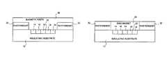
- FIG. 1is an enlarged top view of an exemplary embodiment of a magnetoresistance sensor
- FIG. 2is an enlarged side view of an exemplary embodiment of a magnetoresistance sensor
- FIG. 3is a flow diagram of an exemplary embodiment of a method of integrating a permanent bias magnet within a magnetoresistance sensor
- FIG. 4is a schematic diagram of an exemplary embodiment of a step in a method of integrating a permanent bias magnet within a magnetoresistance sensor
- FIG. 5is a schematic diagram of an exemplary embodiment of a step in a method of integrating a permanent bias magnet within a magnetoresistance sensor
- FIG. 6is a schematic diagram of an exemplary embodiment of a step in a method of integrating a permanent bias magnet within a magnetoresistance sensor
- FIG. 7is a schematic diagram of an exemplary embodiment of a step in a method of integrating a permanent bias magnet within a magnetoresistance sensor
- FIG. 8is a schematic diagram of an exemplary embodiment of a step in a method of integrating a permanent bias magnet within a magnetoresistance sensor
- FIG. 9is a schematic diagram of an exemplary embodiment of a step in a method of integrating a permanent bias magnet within a magnetoresistance sensor.
- FIG. 10is a schematic diagram of an exemplary embodiment of a magnetoresistance sensor with an integrated permanent bias magnet.
- FIG. 1illustrates an enlarged top view of an exemplary embodiment of a magnetoresistance sensor 10 .
- a magnetoresistance deviceis a device that provides a change in electrical resistance of a conductor or semiconductor when a magnetic field is applied. The device's resistance depends upon the magnetic field applied.
- the magnetoresistance sensor 10comprises an insulating substrate 12 , an alternating pattern of a metal material 14 and a semiconductor material 16 deposited on a surface 18 of the insulating substrate, and a bias magnet material 20 deposited over the alternating pattern of metal material 14 and semiconductor material 16 .
- FIG. 2illustrates an enlarged side view of an exemplary embodiment of a magnetoresistance sensor 10 .
- the alternating pattern of metal material 14 and semiconductor material 16creates a composite structure with alternating bands of metal material 14 and semiconductor material 16 .
- At least one input connection contact 22is coupled to the metal material 14 and at least one output connection contact 24 is coupled to the metal material 14 .
- the semiconductor material 16may be series connected to increase the magnetoresistance sensor 10 resistance.
- the semiconductor material 16may be comprised of a single semiconductor element.
- the bias magnet material 20subjects the semiconductor material 16 to a magnetic field required to achieve required sensitivity.
- the magnetoresistance sensor 10provides a signal in response to the strength and direction of a magnetic field.
- the magnetic fieldmay be approximately 0.1 to 0.2 Tesla.
- the application of a magnetic fieldconfines the electrons to the semiconductor material 16 , resulting in an increased path length. Increasing the path length, increases the sensitivity of the magnetoresistance sensor 10 .
- the magnetic fieldalso increases the resistance of the magnetoresistance sensor 10 . In the geometry disclosed in FIGS. 1 and 2 , at a zero magnetic field, the current density is uniform throughout the magnetoresistance sensor 10 . At a high magnetic field, the electrons (or holes) propagate radially outward toward the corners of the semiconductor material 16 , resulting in a large magnetoresistance (high resistance).
- the form factor of the magnetoresistance sensor 10may be scaled to sizes less than 0.1 mm x 0.1 mm.
- the magnetoresistance sensormay be built with various architectures and geometries, including, giant magnetoresistance (GMR) sensors, and extraordinary magnetoresistance (EMR) sensors.
- GMRgiant magnetoresistance
- EMRextraordinary magnetoresistance
- the magnetoresistance sensor 10provides a very small form factor, excellent signal-to-noise ratio (low noise operation), and excellent low frequency response. Low noise combined with wide dynamic range enables the magnetoresistance sensor 10 to be used for position and orientation tracking. The low frequency response of the magnetoresistance sensor 10 allows a position and orientation tracking system to operate at very low frequencies where metal tolerance is maximized.
- FIG. 3illustrates a flow diagram of an exemplary embodiment of a method 50 of integrating a permanent bias magnet within a magnetoresistance sensor.
- the method 50begins with depositing an alternating pattern of a metal material and a semiconductor material on or within a surface of an insulating substrate 52 .
- This step 52is illustrated in FIG. 4 and described in more detail below with reference to FIG. 4 .
- Another step of the method 50includes depositing a photoresist mask on the surface of the insulating substrate in a pattern that covers the surface of the insulating substrate, but does not cover the alternating pattern of metal material and semiconductor material 54 .
- This step 54is illustrated in FIG. 5 and described in more detail below with reference to FIG. 5 .
- the next step of the methodincludes applying a magnetic paste over the photoresist mask and the exposed alternating pattern of metal material and semiconductor material in opening 56 .
- This step 56is illustrated in FIG. 6 and described in more detail below with reference to FIG. 6 .
- the next step of the methodincludes removing the magnetic paste from the photoresist mask 58 .
- This step 58is illustrated in FIG. 7 and described in more detail below with reference to FIG. 7 .
- the next step of the methodincludes curing the magnetic paste left in the openings to form bias magnets above the alternating pattern of metal material and semiconductor material 60 .
- This step 60is illustrated in FIG. 8 and described in more detail below with reference to FIG. 8 .
- the next step of the methodincludes removing the photoresist mask 62 .
- This step 62is illustrated in FIG. 9 and described in more detail below with reference to FIG. 9 .
- the last step in the processis applying a strong magnetic field to magnetize the bias magnets 64 .
- This step 64is illustrated in FIG. 10 and described in more detail below with reference to FIG. 10 .
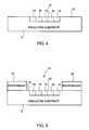
- FIG. 4illustrates an enlarged side schematic diagram of an exemplary embodiment of step 52 in method 50 of integrating a permanent bias magnet within a magnetoresistance sensor.
- a method of producing a plurality of magnetoresistance sensorsinvolves fabricating an insulating substrate wafer with a plurality of magnetoresistance sensors.
- the active area of a single magnetoresistance sensoris approximately 0.05 mm to 5 mm.
- the approximate size of an insulating substrate waferis approximately 25 mm to 1 m.
- the method 50begins with step 52 of depositing an alternating pattern of a metal material 14 and a semiconductor material 16 on or within a surface 18 of an insulating substrate 12 .
- FIG. 5illustrates an enlarged side schematic diagram of an exemplary embodiment of step 54 in method 50 of integrating a permanent bias magnet within a magnetoresistance sensor.
- the next step 54 of the method 50includes depositing a photoresist mask 32 on the surface 18 of the insulating substrate 12 in a pattern to cover the surface 18 of the insulating substrate 12 , but not cover the alternating pattern of metal material 14 and semiconductor material 16 .
- the photoresist mask 32is used to create an opening 34 above the alternating pattern of metal material 14 and semiconductor material 16 where a permanent bias magnet may be formed.
- the photoresist mask 32is registered with the alternating pattern of metal material 14 and semiconductor material 16 .
- the photoresist mask 32may be deposited and patterned using a lithographic mask or other techniques known in the art.
- photoresistexamples include AZ50XT from AZ Chemicals, Inc., SIPR 7126M from Shin-Etsu MicroSi, Inc., and WB3100 or WBR2100 from E. I. du Pont de Nemours and Company.
- a stencil or a screen printed maskmay be used instead of a photoresist mask, to define the areas where the permanent magnets are to be formed.
- a subtractive processsuch as laser ablation, diamond sawing or chemical etching may be used to define the areas where the permanent magnets are to be formed.
- FIG. 6illustrates an enlarged side schematic diagram of an exemplary embodiment of step 56 in method 50 of integrating a permanent bias magnet within a magnetoresistance sensor.
- the next step 56 of the method 50includes applying a magnetic paste 36 over the photoresist mask 32 and the exposed alternating pattern of metal material 14 and semiconductor material 16 in opening 34 .
- the magnetic paste 36may include a magnetic powder and a binder that are blended together and applied over the photoresist mask 32 and the exposed alternating pattern of metal material 14 and semiconductor material 16 in opening 34 .
- Examples of magnetic powder that may be usedinclude Neodymium Iron Boron (NdFeB) from Magnequench International, Inc., a magnetic powder being identified as MQP-S- 11 - 9 from Magnequench, International, Inc., Samarium Iron Nitrogen (SmFeN) from Sumitomo Metal Mining Co., Ltd., Samarium Cobalt (SmCo) from Alfa Aesar, Cobalt Platinum (CoPt), or Iron Platinum (FePt).
- Examples of the binder that may be usedinclude Epo-Tek 360, a low viscosity two-part epoxy from Epoxy Technology, Inc. or 9-20557, a UV curable epoxy (conformal coating) from Dymax Corporation.
- FIG. 7illustrates an enlarged side schematic diagram of an exemplary embodiment of steps 58 and 60 in method 50 of integrating a permanent bias magnet within a magnetoresistance sensor.
- the next steps 58 and 60 of the method 50include removing the magnetic paste 36 above the photoresist mask 32 and curing the remaining magnetic paste 36 within the opening 34 above the exposed alternating pattern of metal material 14 and semiconductor material 16 to form a hardened bias magnet 20 .
- the curing processmay include 24 hours at room temperature, 24 hours at 60 degrees Celsius and 24 hours at 70 degrees Celsius. It is important that the photoresist does not flow during the curing process.
- FIG. 8illustrates an enlarged side schematic diagram of an exemplary embodiment of step 62 in method 50 of integrating a permanent bias magnet within a magnetoresistance sensor.
- the next step 62 of the method 50includes removing the photoresist mask 32 from around hardened bias magnet 20 .
- the photoresist mask 32may be removed using a suitable stripping chemical such as acetone or N-methyl 2 -pyrrolidone (NMP).
- NMPN-methyl 2 -pyrrolidone
- the stripping processmay include an acetone spray for 30 seconds at room temperature. It is important that the stripping process does not attack the binder.
- the permanent bias magnetsmay be fabricated on a separate substrate and then bonded (including the separate substrate) to the magnetoresistance sensor substrate.
- FIG. 9illustrates an enlarged side schematic diagram of an exemplary embodiment of step 64 in method 50 of integrating a permanent bias magnet within a magnetoresistance sensor.
- the next step 64 of the method 50includes applying a strong magnetic field 40 to magnetize the bias magnet 20 .
- the bias magnet 20(micromanget) is magnetized by placing the magnetoresistance sensor in a strong magnetic field at the desired orientation.
- the applied magnetic fieldmay be approximately between 1 to 5 Tesla, depending upon the magnetic material's coercivity.
- the desired orientation of the magnetoresistance sensor within the strong magnetic fieldmay be a perpendicular or parallel orientation.
- FIG. 10illustrates an enlarged side schematic diagram of an exemplary embodiment of an alternating pattern of metal material 14 and semiconductor material 16 with an integrated permanent bias magnet 20 forming a magnetoresistance sensor 10 .
- the permanent bias magnet 20After removal from the magnetizer, the permanent bias magnet 20 generates a large perpendicular field over the magnetoresistance sensor 10 active area.
- the magnetic flux lines 42are shown in FIG. 10 .
- the permanent bias magnet 20 footprintmay be approximately 0.25 mm ⁇ 0.25 mm. This footprint may be controlled by the photoresist mask opening 34 .
- the permanent bias magnet 20 heightmay be approximately 0.2 mm. This height may be controlled by photoresist mask 32 thickness.
- the present disclosureprovides a method for low-cost integration of micron-scale permanent bias magnets within magnetoresistance sensors.
- the present disclosureprovides a method for generating a strong, relatively uniform perpendicular magnetic bias field for magnetoresistance sensors.
- the perpendicular magnetic bias fieldmay be used to maximize the sensitivity of the magnetoresistance sensors.
Landscapes
- Physics & Mathematics (AREA)
- Engineering & Computer Science (AREA)
- Condensed Matter Physics & Semiconductors (AREA)
- General Physics & Mathematics (AREA)
- Chemical & Material Sciences (AREA)
- Nanotechnology (AREA)
- Manufacturing & Machinery (AREA)
- Crystallography & Structural Chemistry (AREA)
- Measuring Magnetic Variables (AREA)
- Hall/Mr Elements (AREA)
Abstract
Description
Claims (16)
Priority Applications (1)
| Application Number | Priority Date | Filing Date | Title |
|---|---|---|---|
| US12/642,968US8173446B2 (en) | 2009-12-21 | 2009-12-21 | Method of producing an integrated micromagnet sensor assembly |
Applications Claiming Priority (1)
| Application Number | Priority Date | Filing Date | Title |
|---|---|---|---|
| US12/642,968US8173446B2 (en) | 2009-12-21 | 2009-12-21 | Method of producing an integrated micromagnet sensor assembly |
Publications (2)
| Publication Number | Publication Date |
|---|---|
| US20110151587A1 US20110151587A1 (en) | 2011-06-23 |
| US8173446B2true US8173446B2 (en) | 2012-05-08 |
Family
ID=44151669
Family Applications (1)
| Application Number | Title | Priority Date | Filing Date |
|---|---|---|---|
| US12/642,968Active2030-05-20US8173446B2 (en) | 2009-12-21 | 2009-12-21 | Method of producing an integrated micromagnet sensor assembly |
Country Status (1)
| Country | Link |
|---|---|
| US (1) | US8173446B2 (en) |
Families Citing this family (4)
| Publication number | Priority date | Publication date | Assignee | Title |
|---|---|---|---|---|
| US8618795B1 (en) | 2012-06-29 | 2013-12-31 | General Electric Company | Sensor assembly for use in medical position and orientation tracking |
| DE102019211970A1 (en)* | 2019-08-09 | 2021-02-11 | Fraunhofer-Gesellschaft zur Förderung der angewandten Forschung e.V. | A method of manufacturing a printed magnetic functional element and a printed magnetic functional element |
| US11923133B2 (en)* | 2021-11-30 | 2024-03-05 | Ford Global Technologies, Llc | Additive manufacturing of Nd-Fe-B magnets with insulating layers |
| DE102022208562A1 (en) | 2022-08-18 | 2024-02-29 | Fraunhofer-Gesellschaft zur Förderung der angewandten Forschung eingetragener Verein | METHOD FOR PRODUCING A MAGNETIC FIELD SENSOR CHIP WITH AN INTEGRATED BACK-BIAS MAGNET |
Citations (36)
| Publication number | Priority date | Publication date | Assignee | Title |
|---|---|---|---|---|
| US3892603A (en) | 1971-09-01 | 1975-07-01 | Raytheon Co | Method of making magnets |
| EP0042707A1 (en) | 1980-06-13 | 1981-12-30 | Securitas International Products Limited | Token reader |
| US5729129A (en) | 1995-06-07 | 1998-03-17 | Biosense, Inc. | Magnetic location system with feedback adjustment of magnetic field generator |
| US5752513A (en) | 1995-06-07 | 1998-05-19 | Biosense, Inc. | Method and apparatus for determining position of object |
| US5782765A (en) | 1996-04-25 | 1998-07-21 | Medtronic, Inc. | Medical positioning system |
| US5893206A (en) | 1997-02-04 | 1999-04-13 | Eastman Kodak Company | Method for the formation and polarization of micromagnets |
| US5982177A (en)* | 1997-08-08 | 1999-11-09 | Florida State University | Magnetoresistive sensor magnetically biased in a region spaced from a sensing region |
| WO1999060370A2 (en) | 1998-05-15 | 1999-11-25 | Robin Medical, Inc. | Method and apparatus for generating controlled torques |
| WO2000032179A2 (en) | 1998-12-01 | 2000-06-08 | University Of Kentucky Research Foundation | Use of nicotonic acid derivatives for the treatment of dna damage in skin cells |
| US6172499B1 (en) | 1999-10-29 | 2001-01-09 | Ascension Technology Corporation | Eddy current error-reduced AC magnetic position measurement system |
| US6211666B1 (en) | 1996-02-27 | 2001-04-03 | Biosense, Inc. | Object location system and method using field actuation sequences having different field strengths |
| US6241671B1 (en) | 1998-11-03 | 2001-06-05 | Stereotaxis, Inc. | Open field system for magnetic surgery |
| US6246231B1 (en) | 1999-07-29 | 2001-06-12 | Ascension Technology Corporation | Magnetic field permeable barrier for magnetic position measurement system |
| US6427079B1 (en) | 1999-08-09 | 2002-07-30 | Cormedica Corporation | Position and orientation measuring with magnetic fields |
| US6493573B1 (en) | 1999-10-28 | 2002-12-10 | Winchester Development Associates | Method and system for navigating a catheter probe in the presence of field-influencing objects |
| JP2002365010A (en) | 2001-06-05 | 2002-12-18 | Ascension Technology Corp | Magnetic position measurement system provided with magnetic field closure means |
| US20030011359A1 (en) | 2001-07-03 | 2003-01-16 | Ascension Technology Corporation | Magnetic position measurement system with field containment means |
| US20030173953A1 (en) | 2002-03-18 | 2003-09-18 | Ascension Technology Corporation | Low distortion magnetic transmitter and method of operating |
| US6636757B1 (en) | 2001-06-04 | 2003-10-21 | Surgical Navigation Technologies, Inc. | Method and apparatus for electromagnetic navigation of a surgical probe near a metal object |
| US20030233042A1 (en) | 2002-06-18 | 2003-12-18 | Ascension Technology Corporation | Spiral magnetic transmitter for position measurement system |
| US6676813B1 (en) | 2001-03-19 | 2004-01-13 | The Regents Of The University Of California | Technology for fabrication of a micromagnet on a tip of a MFM/MRFM probe |
| US6690963B2 (en) | 1995-01-24 | 2004-02-10 | Biosense, Inc. | System for determining the location and orientation of an invasive medical instrument |
| US6701179B1 (en) | 1999-10-28 | 2004-03-02 | Michael A. Martinelli | Coil structures and methods for generating magnetic fields |
| US6789043B1 (en) | 1998-09-23 | 2004-09-07 | The Johns Hopkins University | Magnetic sensor system for fast-response, high resolution, high accuracy, three-dimensional position measurements |
| US6812842B2 (en) | 2001-12-20 | 2004-11-02 | Calypso Medical Technologies, Inc. | System for excitation of a leadless miniature marker |
| US6822570B2 (en) | 2001-12-20 | 2004-11-23 | Calypso Medical Technologies, Inc. | System for spatially adjustable excitation of leadless miniature marker |
| US6838990B2 (en) | 2001-12-20 | 2005-01-04 | Calypso Medical Technologies, Inc. | System for excitation leadless miniature marker |
| US20050245821A1 (en) | 2004-03-05 | 2005-11-03 | Assaf Govari | Position sensing system for orthopedic applications |
| US20050261566A1 (en) | 2000-12-21 | 2005-11-24 | Peter Hanley | Magnetic field generating system and method |
| US20060023369A1 (en)* | 2004-07-30 | 2006-02-02 | Carey Matthew J | Extraordinary magnetoresistance sensor with perpendicular magnetic biasing by a ferromagnetic multilayer |
| US7174202B2 (en) | 1992-08-14 | 2007-02-06 | British Telecommunications | Medical navigation apparatus |
| US20070078334A1 (en) | 2005-10-04 | 2007-04-05 | Ascension Technology Corporation | DC magnetic-based position and orientation monitoring system for tracking medical instruments |
| US7324915B2 (en) | 2005-07-14 | 2008-01-29 | Biosense Webster, Inc. | Data transmission to a position sensor |
| US7373271B1 (en) | 2004-09-20 | 2008-05-13 | Ascension Technology Corporation | System and method for measuring position and orientation using distortion-compensated magnetic fields |
| US7402996B2 (en) | 2004-03-31 | 2008-07-22 | Japan Science And Technology Agency | Instrument and method for measuring three-dimensional motion |
| US20080269596A1 (en) | 2004-03-10 | 2008-10-30 | Ian Revie | Orthpaedic Monitoring Systems, Methods, Implants and Instruments |
- 2009
- 2009-12-21USUS12/642,968patent/US8173446B2/enactiveActive
Patent Citations (41)
| Publication number | Priority date | Publication date | Assignee | Title |
|---|---|---|---|---|
| US3892603A (en) | 1971-09-01 | 1975-07-01 | Raytheon Co | Method of making magnets |
| EP0042707A1 (en) | 1980-06-13 | 1981-12-30 | Securitas International Products Limited | Token reader |
| US7174202B2 (en) | 1992-08-14 | 2007-02-06 | British Telecommunications | Medical navigation apparatus |
| US6690963B2 (en) | 1995-01-24 | 2004-02-10 | Biosense, Inc. | System for determining the location and orientation of an invasive medical instrument |
| US5729129A (en) | 1995-06-07 | 1998-03-17 | Biosense, Inc. | Magnetic location system with feedback adjustment of magnetic field generator |
| US5752513A (en) | 1995-06-07 | 1998-05-19 | Biosense, Inc. | Method and apparatus for determining position of object |
| US6211666B1 (en) | 1996-02-27 | 2001-04-03 | Biosense, Inc. | Object location system and method using field actuation sequences having different field strengths |
| US5782765A (en) | 1996-04-25 | 1998-07-21 | Medtronic, Inc. | Medical positioning system |
| US5893206A (en) | 1997-02-04 | 1999-04-13 | Eastman Kodak Company | Method for the formation and polarization of micromagnets |
| US5982177A (en)* | 1997-08-08 | 1999-11-09 | Florida State University | Magnetoresistive sensor magnetically biased in a region spaced from a sensing region |
| WO1999060370A2 (en) | 1998-05-15 | 1999-11-25 | Robin Medical, Inc. | Method and apparatus for generating controlled torques |
| US6789043B1 (en) | 1998-09-23 | 2004-09-07 | The Johns Hopkins University | Magnetic sensor system for fast-response, high resolution, high accuracy, three-dimensional position measurements |
| US6241671B1 (en) | 1998-11-03 | 2001-06-05 | Stereotaxis, Inc. | Open field system for magnetic surgery |
| WO2000032179A2 (en) | 1998-12-01 | 2000-06-08 | University Of Kentucky Research Foundation | Use of nicotonic acid derivatives for the treatment of dna damage in skin cells |
| US6246231B1 (en) | 1999-07-29 | 2001-06-12 | Ascension Technology Corporation | Magnetic field permeable barrier for magnetic position measurement system |
| US6427079B1 (en) | 1999-08-09 | 2002-07-30 | Cormedica Corporation | Position and orientation measuring with magnetic fields |
| US6493573B1 (en) | 1999-10-28 | 2002-12-10 | Winchester Development Associates | Method and system for navigating a catheter probe in the presence of field-influencing objects |
| US6701179B1 (en) | 1999-10-28 | 2004-03-02 | Michael A. Martinelli | Coil structures and methods for generating magnetic fields |
| US6172499B1 (en) | 1999-10-29 | 2001-01-09 | Ascension Technology Corporation | Eddy current error-reduced AC magnetic position measurement system |
| US20050261566A1 (en) | 2000-12-21 | 2005-11-24 | Peter Hanley | Magnetic field generating system and method |
| US6676813B1 (en) | 2001-03-19 | 2004-01-13 | The Regents Of The University Of California | Technology for fabrication of a micromagnet on a tip of a MFM/MRFM probe |
| US6636757B1 (en) | 2001-06-04 | 2003-10-21 | Surgical Navigation Technologies, Inc. | Method and apparatus for electromagnetic navigation of a surgical probe near a metal object |
| JP2002365010A (en) | 2001-06-05 | 2002-12-18 | Ascension Technology Corp | Magnetic position measurement system provided with magnetic field closure means |
| US20030011359A1 (en) | 2001-07-03 | 2003-01-16 | Ascension Technology Corporation | Magnetic position measurement system with field containment means |
| US6528991B2 (en) | 2001-07-03 | 2003-03-04 | Ascension Technology Corporation | Magnetic position measurement system with field containment means |
| US6812842B2 (en) | 2001-12-20 | 2004-11-02 | Calypso Medical Technologies, Inc. | System for excitation of a leadless miniature marker |
| US6822570B2 (en) | 2001-12-20 | 2004-11-23 | Calypso Medical Technologies, Inc. | System for spatially adjustable excitation of leadless miniature marker |
| US6838990B2 (en) | 2001-12-20 | 2005-01-04 | Calypso Medical Technologies, Inc. | System for excitation leadless miniature marker |
| US20080001756A1 (en) | 2001-12-20 | 2008-01-03 | Calypso Medical Technologies, Inc. | System for spatially adjustable excitation of leadless miniature marker |
| US7176798B2 (en) | 2001-12-20 | 2007-02-13 | Calypso Medical Technologies, Inc. | System for spatially adjustable excitation of leadless miniature marker |
| US6784660B2 (en) | 2002-03-18 | 2004-08-31 | Ascension Technology Corporation | Magnetic position and orientation measurement system with magnetic field permeable attenuator |
| US20030173953A1 (en) | 2002-03-18 | 2003-09-18 | Ascension Technology Corporation | Low distortion magnetic transmitter and method of operating |
| US20030233042A1 (en) | 2002-06-18 | 2003-12-18 | Ascension Technology Corporation | Spiral magnetic transmitter for position measurement system |
| US6856823B2 (en) | 2002-06-18 | 2005-02-15 | Ascension Technology Corporation | Spiral magnetic transmitter for position measurement system |
| US20050245821A1 (en) | 2004-03-05 | 2005-11-03 | Assaf Govari | Position sensing system for orthopedic applications |
| US20080269596A1 (en) | 2004-03-10 | 2008-10-30 | Ian Revie | Orthpaedic Monitoring Systems, Methods, Implants and Instruments |
| US7402996B2 (en) | 2004-03-31 | 2008-07-22 | Japan Science And Technology Agency | Instrument and method for measuring three-dimensional motion |
| US20060023369A1 (en)* | 2004-07-30 | 2006-02-02 | Carey Matthew J | Extraordinary magnetoresistance sensor with perpendicular magnetic biasing by a ferromagnetic multilayer |
| US7373271B1 (en) | 2004-09-20 | 2008-05-13 | Ascension Technology Corporation | System and method for measuring position and orientation using distortion-compensated magnetic fields |
| US7324915B2 (en) | 2005-07-14 | 2008-01-29 | Biosense Webster, Inc. | Data transmission to a position sensor |
| US20070078334A1 (en) | 2005-10-04 | 2007-04-05 | Ascension Technology Corporation | DC magnetic-based position and orientation monitoring system for tracking medical instruments |
Non-Patent Citations (2)
| Title |
|---|
| Heremans et al, Narrow-gap semiconductor magnetic field sensors and applications, Semicond. Sci. Technol. 8 (1993), S424-S430. |
| Lagorce et al, Magnetic and Mechanical Properties of Micromachined Strontium Ferrite/Polyimide Composites, Journal of Microelectromechanical Systems, vol. 6, No. 4, Dec. 1997, pp. 307-312. |
Also Published As
| Publication number | Publication date |
|---|---|
| US20110151587A1 (en) | 2011-06-23 |
Similar Documents
| Publication | Publication Date | Title |
|---|---|---|
| Gabler et al. | Magnetic origami creates high performance micro devices | |
| US9183979B2 (en) | Chip inductor and method for manufacturing the same | |
| US8173446B2 (en) | Method of producing an integrated micromagnet sensor assembly | |
| Park et al. | Batch-fabricated microinductors with electroplated magnetically anisotropic and laminated alloy cores | |
| TW200912968A (en) | High power inductors using a magnetic basis | |
| US8432164B2 (en) | Ferromagnetic resonance and memory effect in magnetic composite materials | |
| CN108779549B (en) | Evaporation mask, manufacturing method of vapor deposition mask, and manufacturing method of organic semiconductor element | |
| EP1293792A3 (en) | Magnetic detection element utilizing magneto-impedance effect, production method of the element, and portable equipment using the element | |
| US20250157707A1 (en) | Ferromagnetic-Polymer Composite Material and Structures Comprising Same | |
| JP3260921B2 (en) | Movable body displacement detection device | |
| JP2010130012A (en) | Spin valve or tunnel junction high-frequency oscillator | |
| CN101632146A (en) | Magnetic sensor module and piston position detection device | |
| JP2001004726A (en) | Magnetic field sensor | |
| JP2000193407A (en) | Magnetic positioning device | |
| CN102496449A (en) | Method for modulating ferromagnetic/antiferromagnetic double-layer-film pinning field direction | |
| US20220059261A1 (en) | Method for producing a permanent or soft magnet | |
| Jiang et al. | Fabrication of NdFeB microstructures using a silicon molding technique for NdFeB/Ta multilayered films and NdFeB magnetic powder | |
| US20130064991A1 (en) | Manufacturing method of flux gate sensor | |
| US7817463B2 (en) | System and method to fabricate magnetic random access memory | |
| US11923131B2 (en) | Products and applications for the templated fabrication of materials using cold spray deposition | |
| Dey et al. | Study of switching behavior of exchange-coupled nanomagnets by transverse magnetization metrology | |
| Karki et al. | Low voltage local strain enhanced switching of magnetic tunnel junctions | |
| EP4576135A2 (en) | Method for manufacturing ferromagnetic-dielectric composite material | |
| JPWO2011155390A1 (en) | Oscillation element and method for manufacturing the oscillation element | |
| KR101018266B1 (en) | Oscillator with Magnetic Swirl Structure and AC Signal Generation Method Using the Oscillator |
Legal Events
| Date | Code | Title | Description |
|---|---|---|---|
| AS | Assignment | Owner name:GENERAL ELECTRIC COMPANY, NEW YORK Free format text:ASSIGNMENT OF ASSIGNORS INTEREST;ASSIGNOR:HUBER, WILLIAM HULLINGER;REEL/FRAME:023981/0676 Effective date:20100113 | |
| STCF | Information on status: patent grant | Free format text:PATENTED CASE | |
| FPAY | Fee payment | Year of fee payment:4 | |
| AS | Assignment | Owner name:STRYKER EUROPEAN HOLDINGS I, LLC, MICHIGAN Free format text:ASSIGNMENT OF ASSIGNORS INTEREST;ASSIGNOR:GENERAL ELECTRIC COMPANY;REEL/FRAME:046020/0621 Effective date:20171206 | |
| MAFP | Maintenance fee payment | Free format text:PAYMENT OF MAINTENANCE FEE, 8TH YEAR, LARGE ENTITY (ORIGINAL EVENT CODE: M1552); ENTITY STATUS OF PATENT OWNER: LARGE ENTITY Year of fee payment:8 | |
| AS | Assignment | Owner name:STRYKER EUROPEAN HOLDINGS III, LLC, DELAWARE Free format text:NUNC PRO TUNC ASSIGNMENT;ASSIGNOR:STRYKER EUROPEAN HOLDINGS I, LLC;REEL/FRAME:056969/0771 Effective date:20210219 Owner name:STRYKER EUROPEAN OPERATIONS HOLDINGS LLC, MICHIGAN Free format text:CHANGE OF NAME;ASSIGNOR:STRYKER EUROPEAN HOLDINGS III, LLC;REEL/FRAME:056969/0893 Effective date:20190226 | |
| MAFP | Maintenance fee payment | Free format text:PAYMENT OF MAINTENANCE FEE, 12TH YEAR, LARGE ENTITY (ORIGINAL EVENT CODE: M1553); ENTITY STATUS OF PATENT OWNER: LARGE ENTITY Year of fee payment:12 | |
| AS | Assignment | Owner name:STRYKER EUROPEAN OPERATIONS HOLDINGS LLC, MICHIGAN Free format text:CHANGE OF ADDRESS;ASSIGNOR:STRYKER EUROPEAN OPERATIONS HOLDINGS LLC;REEL/FRAME:069730/0754 Effective date:20241217 |