US8171618B1 - Tunable pole trim processes for fabricating trapezoidal perpendicular magnetic recording (PMR) write poles - Google Patents
Tunable pole trim processes for fabricating trapezoidal perpendicular magnetic recording (PMR) write polesDownload PDFInfo
- Publication number
- US8171618B1 US8171618B1US12/486,706US48670609AUS8171618B1US 8171618 B1US8171618 B1US 8171618B1US 48670609 AUS48670609 AUS 48670609AUS 8171618 B1US8171618 B1US 8171618B1
- Authority
- US
- United States
- Prior art keywords
- milling
- angle
- write pole
- side wall
- hard mask
- Prior art date
- Legal status (The legal status is an assumption and is not a legal conclusion. Google has not performed a legal analysis and makes no representation as to the accuracy of the status listed.)
- Expired - Fee Related, expires
Links
- 238000000034methodMethods0.000titleclaimsabstractdescription41
- 230000008569processEffects0.000titledescription10
- 238000003801millingMethods0.000claimsabstractdescription122
- 239000000696magnetic materialSubstances0.000claimsabstractdescription21
- 238000012546transferMethods0.000claimsabstractdescription9
- 230000003068static effectEffects0.000claimsdescription5
- 238000010408sweepingMethods0.000claimsdescription5
- 230000008859changeEffects0.000claimsdescription4
- 229910052751metalInorganic materials0.000claimsdescription4
- 239000002184metalSubstances0.000claimsdescription3
- OKTJSMMVPCPJKN-UHFFFAOYSA-NCarbonChemical compound[C]OKTJSMMVPCPJKN-UHFFFAOYSA-N0.000claimsdescription2
- 239000000956alloySubstances0.000claimsdescription2
- 229910045601alloyInorganic materials0.000claimsdescription2
- 229910052799carbonInorganic materials0.000claimsdescription2
- 239000003989dielectric materialSubstances0.000claimsdescription2
- 229920002120photoresistant polymerPolymers0.000claimsdescription2
- 229920000642polymerPolymers0.000claimsdescription2
- 150000002739metalsChemical class0.000claims1
- 238000010884ion-beam techniqueMethods0.000description13
- 238000000992sputter etchingMethods0.000description11
- 238000004519manufacturing processMethods0.000description6
- 239000000463materialSubstances0.000description6
- 238000010586diagramMethods0.000description5
- 230000015572biosynthetic processEffects0.000description4
- 239000000758substrateSubstances0.000description3
- 230000000694effectsEffects0.000description2
- 238000001000micrographMethods0.000description2
- 238000012986modificationMethods0.000description2
- 230000004048modificationEffects0.000description2
- 230000008685targetingEffects0.000description2
- PNEYBMLMFCGWSK-UHFFFAOYSA-Naluminium oxideInorganic materials[O-2].[O-2].[O-2].[Al+3].[Al+3]PNEYBMLMFCGWSK-UHFFFAOYSA-N0.000description1
- 238000013459approachMethods0.000description1
- 230000001419dependent effectEffects0.000description1
- 238000000151depositionMethods0.000description1
- 238000013461designMethods0.000description1
- 230000001939inductive effectEffects0.000description1
- 239000007769metal materialSubstances0.000description1
- 230000035515penetrationEffects0.000description1
- 238000009877renderingMethods0.000description1
- 238000001878scanning electron micrographMethods0.000description1
- 238000004544sputter depositionMethods0.000description1
Images


Classifications
- G—PHYSICS
- G11—INFORMATION STORAGE
- G11B—INFORMATION STORAGE BASED ON RELATIVE MOVEMENT BETWEEN RECORD CARRIER AND TRANSDUCER
- G11B5/00—Recording by magnetisation or demagnetisation of a record carrier; Reproducing by magnetic means; Record carriers therefor
- G11B5/127—Structure or manufacture of heads, e.g. inductive
- G11B5/1278—Structure or manufacture of heads, e.g. inductive specially adapted for magnetisations perpendicular to the surface of the record carrier
- G—PHYSICS
- G11—INFORMATION STORAGE
- G11B—INFORMATION STORAGE BASED ON RELATIVE MOVEMENT BETWEEN RECORD CARRIER AND TRANSDUCER
- G11B5/00—Recording by magnetisation or demagnetisation of a record carrier; Reproducing by magnetic means; Record carriers therefor
- G11B5/127—Structure or manufacture of heads, e.g. inductive
- G11B5/31—Structure or manufacture of heads, e.g. inductive using thin films
- G11B5/3109—Details
- G11B5/3116—Shaping of layers, poles or gaps for improving the form of the electrical signal transduced, e.g. for shielding, contour effect, equalizing, side flux fringing, cross talk reduction between heads or between heads and information tracks
- G—PHYSICS
- G11—INFORMATION STORAGE
- G11B—INFORMATION STORAGE BASED ON RELATIVE MOVEMENT BETWEEN RECORD CARRIER AND TRANSDUCER
- G11B5/00—Recording by magnetisation or demagnetisation of a record carrier; Reproducing by magnetic means; Record carriers therefor
- G11B5/127—Structure or manufacture of heads, e.g. inductive
- G11B5/31—Structure or manufacture of heads, e.g. inductive using thin films
- G11B5/3163—Fabrication methods or processes specially adapted for a particular head structure, e.g. using base layers for electroplating, using functional layers for masking, using energy or particle beams for shaping the structure or modifying the properties of the basic layers
- Y—GENERAL TAGGING OF NEW TECHNOLOGICAL DEVELOPMENTS; GENERAL TAGGING OF CROSS-SECTIONAL TECHNOLOGIES SPANNING OVER SEVERAL SECTIONS OF THE IPC; TECHNICAL SUBJECTS COVERED BY FORMER USPC CROSS-REFERENCE ART COLLECTIONS [XRACs] AND DIGESTS
- Y10—TECHNICAL SUBJECTS COVERED BY FORMER USPC
- Y10T—TECHNICAL SUBJECTS COVERED BY FORMER US CLASSIFICATION
- Y10T29/00—Metal working
- Y10T29/49—Method of mechanical manufacture
- Y10T29/49002—Electrical device making
- Y10T29/4902—Electromagnet, transformer or inductor
- Y10T29/49021—Magnetic recording reproducing transducer [e.g., tape head, core, etc.]
- Y10T29/49032—Fabricating head structure or component thereof
- Y10T29/49036—Fabricating head structure or component thereof including measuring or testing
- Y10T29/49043—Depositing magnetic layer or coating
- Y10T29/49044—Plural magnetic deposition layers
- Y—GENERAL TAGGING OF NEW TECHNOLOGICAL DEVELOPMENTS; GENERAL TAGGING OF CROSS-SECTIONAL TECHNOLOGIES SPANNING OVER SEVERAL SECTIONS OF THE IPC; TECHNICAL SUBJECTS COVERED BY FORMER USPC CROSS-REFERENCE ART COLLECTIONS [XRACs] AND DIGESTS
- Y10—TECHNICAL SUBJECTS COVERED BY FORMER USPC
- Y10T—TECHNICAL SUBJECTS COVERED BY FORMER US CLASSIFICATION
- Y10T29/00—Metal working
- Y10T29/49—Method of mechanical manufacture
- Y10T29/49002—Electrical device making
- Y10T29/4902—Electromagnet, transformer or inductor
- Y10T29/49021—Magnetic recording reproducing transducer [e.g., tape head, core, etc.]
- Y10T29/49032—Fabricating head structure or component thereof
- Y10T29/49036—Fabricating head structure or component thereof including measuring or testing
- Y10T29/49043—Depositing magnetic layer or coating
- Y10T29/49046—Depositing magnetic layer or coating with etching or machining of magnetic material
- Y—GENERAL TAGGING OF NEW TECHNOLOGICAL DEVELOPMENTS; GENERAL TAGGING OF CROSS-SECTIONAL TECHNOLOGIES SPANNING OVER SEVERAL SECTIONS OF THE IPC; TECHNICAL SUBJECTS COVERED BY FORMER USPC CROSS-REFERENCE ART COLLECTIONS [XRACs] AND DIGESTS
- Y10—TECHNICAL SUBJECTS COVERED BY FORMER USPC
- Y10T—TECHNICAL SUBJECTS COVERED BY FORMER US CLASSIFICATION
- Y10T29/00—Metal working
- Y10T29/49—Method of mechanical manufacture
- Y10T29/49002—Electrical device making
- Y10T29/4902—Electromagnet, transformer or inductor
- Y10T29/49021—Magnetic recording reproducing transducer [e.g., tape head, core, etc.]
- Y10T29/49032—Fabricating head structure or component thereof
- Y10T29/49048—Machining magnetic material [e.g., grinding, etching, polishing]
- Y10T29/49052—Machining magnetic material [e.g., grinding, etching, polishing] by etching
Definitions
- the present inventiongenerally relates to hard disk drives and, in particular, relates to tunable pole trim processes for fabricating trapezoidal perpendicular magnetic recording (“PMR”) write poles.
- PMRtrapezoidal perpendicular magnetic recording
- Hard disk drivesinclude one or more rigid disks, which are coated with a magnetic recording medium in which data can be stored. Hard disk drives further include read and write heads for interacting with the data in the magnetic recording medium.
- the write headincludes an inductive element for generating a magnetic field that aligns the magnetic moments of domains in the magnetic recording medium to represent bits of data.
- Magnetic recording techniquesinclude both longitudinal and perpendicular recording.
- Perpendicular magnetic recording (“PMR”)is a form of magnetic recording in which the magnetic moments representing bits of data are oriented perpendicularly to the surface of the magnetic recording medium, as opposed to longitudinally along a track thereof. PMR enjoys a number of advantages over longitudinal recording, such as significantly higher areal density recording capability.
- Write poles with a trapezoidal cross-sectional shape at the air bearing surface (“ABS”)are used to provide improved writing performance in PMR heads.
- ABSair bearing surface
- the manufacture of write poles with this trapezoidal cross-sectional shapepresents a number of difficulties, however, not the least of which involve providing the pole with both desired side wall angles and desired track width, as these parameters are dependent upon one another in the manufacturing process. In this regard, in some manufacturing processes, attempting to achieve a specific side wall angle may result in an undesirable track width, and vice versa.
- FIG. 1a scanning electron micrograph of a write pole is shown in cross-section.
- FIG. 1a scanning electron micrograph of a write pole is shown in cross-section.
- FIG. 2a distinct “waist” and “footing” can be seen.
- some processesinvolve milling a write pole from a layer of magnetic material disposed over a non-magnetic buffer layer, whereby the footing is formed in the non-magnetic buffer, such that the portion of the structure comprising magnetic material approximates a trapezoidal shape.
- FIG. 2One such configuration is illustrated in FIG. 2 .
- This approachsuffers from notable drawbacks, such as pole protrusion, which can result when the non-magnetic buffer layer is heated during write operations and extends beyond the air bearing surface.
- Various embodiments of the present inventionsolve the foregoing problems by providing tunable pole trim processes for fabricating trapezoidal PMR write poles, in which the side wall angle and track width parameters are largely decoupled.
- the disclosed processesallow for the precise manufacture of PMR write poles with desired side wall angles and track widths, without the inclusion of problematic non-magnetic buffer layers.
- a method of forming a write pole for a magnetic recording devicecomprises providing a layer of magnetic material covered with a secondary hard mask layer and a patterned primary hard mask, a first milling step comprising milling at a first milling angle to transfer a pattern from the patterned primary hard mask to the secondary hard mask, and a second milling step comprising milling at a second milling angle to transfer the pattern from the secondary hard mask to the layer of magnetic material to form the write pole.
- the second milling angleis greater than the first milling angle.
- the methodfurther comprises a third milling step comprising milling at a third milling angle to adjust a side wall angle of the write pole to about a desired side wall angle, and a fourth milling step comprising milling at a fourth milling angle to reduce a track width of the write pole to a desired track width.
- FIG. 1illustrates a trapezoidal write pole having a waist and a footing
- FIG. 2illustrates a trapezoidal write pole formed over a non-magnetic buffer layer
- FIG. 3is a flow chart illustrating a method of forming a write pole for a magnetic recording device in accordance with one aspect of the subject disclosure
- FIG. 4is a block diagram illustrating a layered structure from which a write pole for a magnetic recording device is formed, at one stage of the formation thereof, in accordance with one aspect of the subject disclosure
- FIG. 5is a block diagram illustrating a layered structure from which a write pole for a magnetic recording device is formed, at one stage of the formation thereof, in accordance with one aspect of the subject disclosure
- FIG. 6is a block diagram illustrating a layered structure from which a write pole for a magnetic recording device is formed, at one stage of the formation thereof, in accordance with one aspect of the subject disclosure
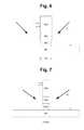
- FIG. 7is a block diagram illustrating a layered structure from which a write pole for a magnetic recording device is formed, at one stage of the formation thereof, in accordance with one aspect of the subject disclosure
- FIG. 8is a block diagram illustrating a write pole for a magnetic recording device, in accordance with one aspect of the subject disclosure
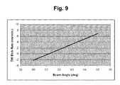
- FIG. 9is a graph illustrating an exemplary relationship between a milling beam angle and a track width etch rate, in accordance with one aspect of the subject disclosure.
- FIG. 10is a graph illustrating an exemplary relationship between a milling beam angle and a side wall angle growth rate, in accordance with one aspect of the subject disclosure.
- FIGS. 11 and 12are scanning electron microscope images of exemplary write poles for magnetic recording devices, in accordance with various aspects of the subject disclosure.
- FIG. 3is a flowchart illustrating a method of forming a write pole for a magnetic recording device in accordance with one aspect of the subject disclosure.
- the methodbegins with step 301 , in which a structure comprising a layer of magnetic material covered with a secondary hard mask layer and a patterned primary hard mask is provided.
- a structurecomprising a layer of magnetic material covered with a secondary hard mask layer and a patterned primary hard mask is provided.
- a substrate layer 401is covered with a layer of magnetic material 402 (e.g., CoNiFe or the like) from which the write pole will be milled.
- the layer of magnetic material 402is covered in turn with a secondary hard mask 403 and a patterned primary hard mask 404 .
- the primary mask layermay be composed of any one of a number of suitable hard mask materials known to those of skill in the art, including, for example, photoresist, a polymer, a metal, an alloy, a dielectric, diamond-like carbon, or some combination thereof.
- the pattern in the primary hard maskmay be configured to provide the overhead shape of the write pole (e.g., a nose region, a yoke region and the like).
- the width of the primary hard maskmay be greater than the desired final track width of the write pole to be formed.
- the height of the primary hard maskmay be selected such that it will withstand the first three milling steps of the ion milling process (as set forth in greater detail below).
- the secondary mask layermay be comprised of any one of a number of suitable hard mask materials, including, for example, one or more layers of metal and/or dielectric materials. As is illustrated in FIG. 4 , the thickness of the secondary mask layer may be substantially the same as a thickness of the layer of magnetic material.
- the secondary hard maskmay be chosen from a material or materials that have low sputtering yield at a high ion beam milling angle ⁇ .
- the processcontinues with a first milling step, in which the structure is milled at a first milling angle ⁇ 1 to transfer a pattern from patterned primary hard mask 404 to secondary hard mask 403 .
- the first milling angle ⁇ 1may be a steep angle (e.g., between about 0° and 20°) to more reliably transfer the pattern from patterned primary hard mask 404 to secondary hard mask 403 .
- This step of ion millingmay be performed in a full rotation (i.e., in which the milling ion beam comes from all 360 degrees of azimuth angle) for better uniformity.
- this ion milling stepmay be performed in either a sweeping fashion (i.e., in which the ion beam comes from a smaller range of azimuth angles) or in a static fashion (i.e., in which the ion beam comes from a fixed azimuth angle). With this trim step some penetration into the magnetic media layer may also be achieved.
- step 302The structure resulting from step 302 is illustrated in exemplary FIG. 5 , in accordance with one aspect of the subject disclosure.
- ion milling at angle ⁇ 1has transferred the pattern from primary hard mask 404 to secondary hard mask 403 and etched part of the way into the layer of magnetic material 402 to leave a desired thickness thereof (which is an important parameter in setting the side wall angle in the following steps).
- step 303the process continues with a second milling step, in which the structure of FIG. 5 is milled at a second milling angle ⁇ 2 to transfer the pattern from the secondary hard mask 403 to the layer of magnetic material 402 in order to form the write pole.
- This step of ion millingmay be performed in a full rotation (i.e., in which the milling ion beam comes from all 360 degrees of azimuth angle) for better uniformity.
- this ion milling stepmay be performed in either a sweeping fashion (i.e., in which the ion beam comes from a smaller range of azimuth angles) or in a static fashion (i.e., in which the ion beam comes from a fixed azimuth angle).
- the second milling anglemay be greater than the first milling angle.
- the second milling anglemay be between about 45° and 70°.
- the second milling stepmay comprise milling the structure of FIG. 5 with a combination of beam angles. All of the beam angles may be greater than the first beam angle of the first milling step.
- at least two anglesmay be used, so that the time ratio between the two angle millings may be manipulated to tune the side wall angle.
- the choice of beam angles and the ratio of time spent milling the different anglescan be configured to achieve a side wall angle in the range of a few degrees to tens of degrees, responding to various design requirements.
- a ratio between the durations of the two angle millings of step 303may be selected to adjust the side wall angle of the write pole to between about 110% and 125% of the desired final side wall angle.
- the side wall anglemay be close to the desired target side wall angle.
- a footingmay also appear at the base of the pole. The footing relieves the pinning effect of the substrate layer 401 and facilitates the generation and tuning of SA.
- the resultant structure following the second milling step 303is illustrated in FIG. 6 , in accordance with one aspect of the subject disclosure.
- the pattern previously transferred from primary hard mask 404 to secondary hard mask 403has now been transferred to the layer of magnetic material 402 .
- the layer of magnetic material 402has been formed into a rough write pole, with a track width (“TW”) and a side wall angle (“SWA”), but also with a “footing” of material where it abuts substrate layer 401 .
- step 304the process continues with a third milling step, in which the structure of FIG. 6 is milled at a third milling angle ⁇ 3 to adjust a side wall angle of the write pole to about a desired side wall angle and to pre-target the desired track width.
- This step of ion millingmay be performed in a full rotation (i.e., in which the milling ion beam comes from all 360 degrees of azimuth angle) for better uniformity.
- this ion milling stepmay be performed in either a sweeping fashion (i.e., in which the ion beam comes from a smaller range of azimuth angles) or in a static fashion (i.e., in which the ion beam comes from a fixed azimuth angle).
- the third milling anglemay be between about 55° and 70°. This step may help to minimize wafer-to-wafer variations in both track width and side wall angle. At the end of this step the footing may or may not remain.
- the side wall anglemay be between about 105% and 110% of the desired final side wall angle.
- the third milling stepmay be further configured to reduce the track width of the write pole to between about 105% and 120% of the desired track width.
- the resultant structure following the third milling step 304is illustrated in FIG. 7 , in accordance with one aspect of the subject disclosure.
- the track width TW of write pole 402has been reduced by the third milling step 304 , and the side wall angle has been adjusted to about 105% to 110% of the final side wall angle.
- write pole 402still retails a footing following the third milling step 304 .
- a milling angle for third milling step 304may be chosen to achieve both a desired track width etch rate and a desired side wall angle growth rate. For example, as can be seen by comparing FIGS. 9 and 10 , choosing a higher beam angle for the third milling step 304 will tune the side wall angle at a slower rate and etch the track width at a faster rate, and vice versa.
- step 305the process continues with a fourth milling step, in which the structure of FIG. 7 is milled at a fourth milling angle ⁇ 4 to reduce the track width of write pole 402 to the desired final track width.
- This step of ion millingmay be performed in a full rotation (i.e., in which the milling ion beam comes from all 360 degrees of azimuth angle) for better uniformity.
- this ion milling stepmay be performed in either a sweeping fashion (i.e., in which the ion beam comes from a smaller range of azimuth angles) or in a static fashion (i.e., in which the ion beam comes from a fixed azimuth angle).
- the third milling anglemay be between about 60° and 70°.
- the fourth milling stepmay also be configured to adjust the side wall angle of the write pole to the desired final side wall angle.
- the fourth milling anglemay be chosen to maximize a rate of change of the track width while minimizing a rate of change of the side wall angle (which has been to about 105% to 110% of the final side wall angle in the previous step).
- the side wall angletends to decrease very slowly, such that the side wall angle targeting is essentially de-coupled from the track width targeting.
- the etch rate for the track widthgoes from negative (i.e., as a result of re-deposition) to positive with increasing beam angle.
- the beam angle and etch time for the fourth milling stepmay be chosen to achieve the track width target while slightly reducing the side wall angle to its final target.
- any footing remaining on the write pole after the third milling stepmay be removed in the fourth milling step. Milling at a shallower angle will remove the footing from the lower edge of the write pole more efficiently. As a result of this milling step, any footing remaining from previous step may be completely removed, producing a simple trapezoidal or triangular cross-sectional shape for the write pole (near the air bearing surface thereof).
- write pole 402has a final track width (“TW”) and a final side wall angle (“SWA”), and has a simple trapezoidal cross-sectional shape.
- TWfinal track width
- SWAfinal side wall angle
- primary hard mask 404may be completely removed by the milling processes.
- the foregoing methodmay be performed iteratively with one or more measuring steps, whereby following a milling step, one or more write poles in a wafer may be measured to determine the progress of the milling operation, in order to select appropriate milling angles and etch times for subsequent milling steps. For example, after the first milling step, the remaining thickness of the layer of magnetic material may be measured to determine an appropriate etch time for the second milling step. Similarly, after the second or third milling steps, the track width and/or side wall angles of one or more write poles in the wafer may be measured to set the parameters for subsequent milling steps.
- FIGS. 11 and 12are scanning electron microscope images of exemplary write poles for magnetic recording devices, in accordance with various aspects of the subject disclosure.
- the write poles 1100 and 1200have simple trapezoidal ( 1100 ) and triangular ( 1200 ) cross sections, are free from any “footing” or “waist,” and do not rest upon a non-magnetic buffer layer.
Landscapes
- Engineering & Computer Science (AREA)
- Manufacturing & Machinery (AREA)
- Magnetic Heads (AREA)
Abstract
Description
Claims (19)
Priority Applications (1)
| Application Number | Priority Date | Filing Date | Title |
|---|---|---|---|
| US12/486,706US8171618B1 (en) | 2009-06-17 | 2009-06-17 | Tunable pole trim processes for fabricating trapezoidal perpendicular magnetic recording (PMR) write poles |
Applications Claiming Priority (1)
| Application Number | Priority Date | Filing Date | Title |
|---|---|---|---|
| US12/486,706US8171618B1 (en) | 2009-06-17 | 2009-06-17 | Tunable pole trim processes for fabricating trapezoidal perpendicular magnetic recording (PMR) write poles |
Publications (1)
| Publication Number | Publication Date |
|---|---|
| US8171618B1true US8171618B1 (en) | 2012-05-08 |
Family
ID=46001959
Family Applications (1)
| Application Number | Title | Priority Date | Filing Date |
|---|---|---|---|
| US12/486,706Expired - Fee RelatedUS8171618B1 (en) | 2009-06-17 | 2009-06-17 | Tunable pole trim processes for fabricating trapezoidal perpendicular magnetic recording (PMR) write poles |
Country Status (1)
| Country | Link |
|---|---|
| US (1) | US8171618B1 (en) |
Cited By (131)
| Publication number | Priority date | Publication date | Assignee | Title |
|---|---|---|---|---|
| US8830628B1 (en) | 2009-02-23 | 2014-09-09 | Western Digital (Fremont), Llc | Method and system for providing a perpendicular magnetic recording head |
| US8879207B1 (en) | 2011-12-20 | 2014-11-04 | Western Digital (Fremont), Llc | Method for providing a side shield for a magnetic recording transducer using an air bridge |
| US8883017B1 (en) | 2013-03-12 | 2014-11-11 | Western Digital (Fremont), Llc | Method and system for providing a read transducer having seamless interfaces |
| US8917581B1 (en) | 2013-12-18 | 2014-12-23 | Western Digital Technologies, Inc. | Self-anneal process for a near field transducer and chimney in a hard disk drive assembly |
| US8923102B1 (en) | 2013-07-16 | 2014-12-30 | Western Digital (Fremont), Llc | Optical grating coupling for interferometric waveguides in heat assisted magnetic recording heads |
| US8947985B1 (en) | 2013-07-16 | 2015-02-03 | Western Digital (Fremont), Llc | Heat assisted magnetic recording transducers having a recessed pole |
| US8953422B1 (en) | 2014-06-10 | 2015-02-10 | Western Digital (Fremont), Llc | Near field transducer using dielectric waveguide core with fine ridge feature |
| US8958272B1 (en) | 2014-06-10 | 2015-02-17 | Western Digital (Fremont), Llc | Interfering near field transducer for energy assisted magnetic recording |
| US8971160B1 (en) | 2013-12-19 | 2015-03-03 | Western Digital (Fremont), Llc | Near field transducer with high refractive index pin for heat assisted magnetic recording |
| US8970988B1 (en) | 2013-12-31 | 2015-03-03 | Western Digital (Fremont), Llc | Electric gaps and method for making electric gaps for multiple sensor arrays |
| US8976635B1 (en) | 2014-06-10 | 2015-03-10 | Western Digital (Fremont), Llc | Near field transducer driven by a transverse electric waveguide for energy assisted magnetic recording |
| US8982508B1 (en) | 2011-10-31 | 2015-03-17 | Western Digital (Fremont), Llc | Method for providing a side shield for a magnetic recording transducer |
| US8980109B1 (en) | 2012-12-11 | 2015-03-17 | Western Digital (Fremont), Llc | Method for providing a magnetic recording transducer using a combined main pole and side shield CMP for a wraparound shield scheme |
| US8984740B1 (en) | 2012-11-30 | 2015-03-24 | Western Digital (Fremont), Llc | Process for providing a magnetic recording transducer having a smooth magnetic seed layer |
| US8988825B1 (en) | 2014-02-28 | 2015-03-24 | Western Digital (Fremont, LLC | Method for fabricating a magnetic writer having half-side shields |
| US8988812B1 (en) | 2013-11-27 | 2015-03-24 | Western Digital (Fremont), Llc | Multi-sensor array configuration for a two-dimensional magnetic recording (TDMR) operation |
| US8993217B1 (en) | 2013-04-04 | 2015-03-31 | Western Digital (Fremont), Llc | Double exposure technique for high resolution disk imaging |
| US8995087B1 (en) | 2006-11-29 | 2015-03-31 | Western Digital (Fremont), Llc | Perpendicular magnetic recording write head having a wrap around shield |
| US8997832B1 (en) | 2010-11-23 | 2015-04-07 | Western Digital (Fremont), Llc | Method of fabricating micrometer scale components |
| US9001628B1 (en) | 2013-12-16 | 2015-04-07 | Western Digital (Fremont), Llc | Assistant waveguides for evaluating main waveguide coupling efficiency and diode laser alignment tolerances for hard disk |
| US9001467B1 (en) | 2014-03-05 | 2015-04-07 | Western Digital (Fremont), Llc | Method for fabricating side shields in a magnetic writer |
| US9007879B1 (en) | 2014-06-10 | 2015-04-14 | Western Digital (Fremont), Llc | Interfering near field transducer having a wide metal bar feature for energy assisted magnetic recording |
| US9007725B1 (en) | 2014-10-07 | 2015-04-14 | Western Digital (Fremont), Llc | Sensor with positive coupling between dual ferromagnetic free layer laminates |
| US9007719B1 (en) | 2013-10-23 | 2015-04-14 | Western Digital (Fremont), Llc | Systems and methods for using double mask techniques to achieve very small features |
| US9013836B1 (en) | 2013-04-02 | 2015-04-21 | Western Digital (Fremont), Llc | Method and system for providing an antiferromagnetically coupled return pole |
| US9042057B1 (en) | 2013-01-09 | 2015-05-26 | Western Digital (Fremont), Llc | Methods for providing magnetic storage elements with high magneto-resistance using Heusler alloys |
| US9042208B1 (en) | 2013-03-11 | 2015-05-26 | Western Digital Technologies, Inc. | Disk drive measuring fly height by applying a bias voltage to an electrically insulated write component of a head |
| US9042058B1 (en) | 2013-10-17 | 2015-05-26 | Western Digital Technologies, Inc. | Shield designed for middle shields in a multiple sensor array |
| US9042052B1 (en) | 2014-06-23 | 2015-05-26 | Western Digital (Fremont), Llc | Magnetic writer having a partially shunted coil |
| US9042051B2 (en) | 2013-08-15 | 2015-05-26 | Western Digital (Fremont), Llc | Gradient write gap for perpendicular magnetic recording writer |
| US9053735B1 (en) | 2014-06-20 | 2015-06-09 | Western Digital (Fremont), Llc | Method for fabricating a magnetic writer using a full-film metal planarization |
| US9064528B1 (en) | 2013-05-17 | 2015-06-23 | Western Digital Technologies, Inc. | Interferometric waveguide usable in shingled heat assisted magnetic recording in the absence of a near-field transducer |
| US9064527B1 (en) | 2013-04-12 | 2015-06-23 | Western Digital (Fremont), Llc | High order tapered waveguide for use in a heat assisted magnetic recording head |
| US9065043B1 (en) | 2012-06-29 | 2015-06-23 | Western Digital (Fremont), Llc | Tunnel magnetoresistance read head with narrow shield-to-shield spacing |
| US9064507B1 (en) | 2009-07-31 | 2015-06-23 | Western Digital (Fremont), Llc | Magnetic etch-stop layer for magnetoresistive read heads |
| US9070381B1 (en) | 2013-04-12 | 2015-06-30 | Western Digital (Fremont), Llc | Magnetic recording read transducer having a laminated free layer |
| US9082423B1 (en) | 2013-12-18 | 2015-07-14 | Western Digital (Fremont), Llc | Magnetic recording write transducer having an improved trailing surface profile |
| US9087527B1 (en) | 2014-10-28 | 2015-07-21 | Western Digital (Fremont), Llc | Apparatus and method for middle shield connection in magnetic recording transducers |
| US9087534B1 (en) | 2011-12-20 | 2015-07-21 | Western Digital (Fremont), Llc | Method and system for providing a read transducer having soft and hard magnetic bias structures |
| US9093639B2 (en) | 2012-02-21 | 2015-07-28 | Western Digital (Fremont), Llc | Methods for manufacturing a magnetoresistive structure utilizing heating and cooling |
| US9104107B1 (en) | 2013-04-03 | 2015-08-11 | Western Digital (Fremont), Llc | DUV photoresist process |
| US9111558B1 (en) | 2014-03-14 | 2015-08-18 | Western Digital (Fremont), Llc | System and method of diffractive focusing of light in a waveguide |
| US9111564B1 (en) | 2013-04-02 | 2015-08-18 | Western Digital (Fremont), Llc | Magnetic recording writer having a main pole with multiple flare angles |
| US9111550B1 (en) | 2014-12-04 | 2015-08-18 | Western Digital (Fremont), Llc | Write transducer having a magnetic buffer layer spaced between a side shield and a write pole by non-magnetic layers |
| US9123362B1 (en) | 2011-03-22 | 2015-09-01 | Western Digital (Fremont), Llc | Methods for assembling an electrically assisted magnetic recording (EAMR) head |
| US9123358B1 (en) | 2012-06-11 | 2015-09-01 | Western Digital (Fremont), Llc | Conformal high moment side shield seed layer for perpendicular magnetic recording writer |
| US9123359B1 (en) | 2010-12-22 | 2015-09-01 | Western Digital (Fremont), Llc | Magnetic recording transducer with sputtered antiferromagnetic coupling trilayer between plated ferromagnetic shields and method of fabrication |
| US9123374B1 (en) | 2015-02-12 | 2015-09-01 | Western Digital (Fremont), Llc | Heat assisted magnetic recording writer having an integrated polarization rotation plate |
| US9135937B1 (en) | 2014-05-09 | 2015-09-15 | Western Digital (Fremont), Llc | Current modulation on laser diode for energy assisted magnetic recording transducer |
| US9135930B1 (en) | 2014-03-06 | 2015-09-15 | Western Digital (Fremont), Llc | Method for fabricating a magnetic write pole using vacuum deposition |
| US9142233B1 (en) | 2014-02-28 | 2015-09-22 | Western Digital (Fremont), Llc | Heat assisted magnetic recording writer having a recessed pole |
| US9147408B1 (en) | 2013-12-19 | 2015-09-29 | Western Digital (Fremont), Llc | Heated AFM layer deposition and cooling process for TMR magnetic recording sensor with high pinning field |
| US9147404B1 (en) | 2015-03-31 | 2015-09-29 | Western Digital (Fremont), Llc | Method and system for providing a read transducer having a dual free layer |
| US9153255B1 (en) | 2014-03-05 | 2015-10-06 | Western Digital (Fremont), Llc | Method for fabricating a magnetic writer having an asymmetric gap and shields |
| US9183854B2 (en) | 2014-02-24 | 2015-11-10 | Western Digital (Fremont), Llc | Method to make interferometric taper waveguide for HAMR light delivery |
| US9190085B1 (en) | 2014-03-12 | 2015-11-17 | Western Digital (Fremont), Llc | Waveguide with reflective grating for localized energy intensity |
| US9190079B1 (en) | 2014-09-22 | 2015-11-17 | Western Digital (Fremont), Llc | Magnetic write pole having engineered radius of curvature and chisel angle profiles |
| US9194692B1 (en) | 2013-12-06 | 2015-11-24 | Western Digital (Fremont), Llc | Systems and methods for using white light interferometry to measure undercut of a bi-layer structure |
| US9202493B1 (en) | 2014-02-28 | 2015-12-01 | Western Digital (Fremont), Llc | Method of making an ultra-sharp tip mode converter for a HAMR head |
| US9202480B2 (en) | 2009-10-14 | 2015-12-01 | Western Digital (Fremont), LLC. | Double patterning hard mask for damascene perpendicular magnetic recording (PMR) writer |
| US9213322B1 (en) | 2012-08-16 | 2015-12-15 | Western Digital (Fremont), Llc | Methods for providing run to run process control using a dynamic tuner |
| US9214165B1 (en) | 2014-12-18 | 2015-12-15 | Western Digital (Fremont), Llc | Magnetic writer having a gradient in saturation magnetization of the shields |
| US9214172B2 (en) | 2013-10-23 | 2015-12-15 | Western Digital (Fremont), Llc | Method of manufacturing a magnetic read head |
| US9214169B1 (en) | 2014-06-20 | 2015-12-15 | Western Digital (Fremont), Llc | Magnetic recording read transducer having a laminated free layer |
| US9230565B1 (en) | 2014-06-24 | 2016-01-05 | Western Digital (Fremont), Llc | Magnetic shield for magnetic recording head |
| US9236560B1 (en) | 2014-12-08 | 2016-01-12 | Western Digital (Fremont), Llc | Spin transfer torque tunneling magnetoresistive device having a laminated free layer with perpendicular magnetic anisotropy |
| US9245562B1 (en) | 2015-03-30 | 2016-01-26 | Western Digital (Fremont), Llc | Magnetic recording writer with a composite main pole |
| US9245545B1 (en) | 2013-04-12 | 2016-01-26 | Wester Digital (Fremont), Llc | Short yoke length coils for magnetic heads in disk drives |
| US9245543B1 (en) | 2010-06-25 | 2016-01-26 | Western Digital (Fremont), Llc | Method for providing an energy assisted magnetic recording head having a laser integrally mounted to the slider |
| US9251813B1 (en) | 2009-04-19 | 2016-02-02 | Western Digital (Fremont), Llc | Method of making a magnetic recording head |
| US9263067B1 (en) | 2013-05-29 | 2016-02-16 | Western Digital (Fremont), Llc | Process for making PMR writer with constant side wall angle |
| US9263071B1 (en) | 2015-03-31 | 2016-02-16 | Western Digital (Fremont), Llc | Flat NFT for heat assisted magnetic recording |
| US9269382B1 (en) | 2012-06-29 | 2016-02-23 | Western Digital (Fremont), Llc | Method and system for providing a read transducer having improved pinning of the pinned layer at higher recording densities |
| US9275657B1 (en) | 2013-08-14 | 2016-03-01 | Western Digital (Fremont), Llc | Process for making PMR writer with non-conformal side gaps |
| US9280990B1 (en) | 2013-12-11 | 2016-03-08 | Western Digital (Fremont), Llc | Method for fabricating a magnetic writer using multiple etches |
| US9286919B1 (en) | 2014-12-17 | 2016-03-15 | Western Digital (Fremont), Llc | Magnetic writer having a dual side gap |
| US9287494B1 (en) | 2013-06-28 | 2016-03-15 | Western Digital (Fremont), Llc | Magnetic tunnel junction (MTJ) with a magnesium oxide tunnel barrier |
| US9305583B1 (en) | 2014-02-18 | 2016-04-05 | Western Digital (Fremont), Llc | Method for fabricating a magnetic writer using multiple etches of damascene materials |
| US9312064B1 (en) | 2015-03-02 | 2016-04-12 | Western Digital (Fremont), Llc | Method to fabricate a magnetic head including ion milling of read gap using dual layer hard mask |
| US9318130B1 (en) | 2013-07-02 | 2016-04-19 | Western Digital (Fremont), Llc | Method to fabricate tunneling magnetic recording heads with extended pinned layer |
| US9336814B1 (en) | 2013-03-12 | 2016-05-10 | Western Digital (Fremont), Llc | Inverse tapered waveguide for use in a heat assisted magnetic recording head |
| US9343086B1 (en) | 2013-09-11 | 2016-05-17 | Western Digital (Fremont), Llc | Magnetic recording write transducer having an improved sidewall angle profile |
| US9343098B1 (en) | 2013-08-23 | 2016-05-17 | Western Digital (Fremont), Llc | Method for providing a heat assisted magnetic recording transducer having protective pads |
| US9343087B1 (en) | 2014-12-21 | 2016-05-17 | Western Digital (Fremont), Llc | Method for fabricating a magnetic writer having half shields |
| US9349392B1 (en) | 2012-05-24 | 2016-05-24 | Western Digital (Fremont), Llc | Methods for improving adhesion on dielectric substrates |
| US9349394B1 (en) | 2013-10-18 | 2016-05-24 | Western Digital (Fremont), Llc | Method for fabricating a magnetic writer having a gradient side gap |
| US9361913B1 (en) | 2013-06-03 | 2016-06-07 | Western Digital (Fremont), Llc | Recording read heads with a multi-layer AFM layer methods and apparatuses |
| US9361914B1 (en) | 2014-06-18 | 2016-06-07 | Western Digital (Fremont), Llc | Magnetic sensor with thin capping layer |
| US9368134B1 (en) | 2010-12-16 | 2016-06-14 | Western Digital (Fremont), Llc | Method and system for providing an antiferromagnetically coupled writer |
| US9384763B1 (en) | 2015-03-26 | 2016-07-05 | Western Digital (Fremont), Llc | Dual free layer magnetic reader having a rear bias structure including a soft bias layer |
| US9384765B1 (en) | 2015-09-24 | 2016-07-05 | Western Digital (Fremont), Llc | Method and system for providing a HAMR writer having improved optical efficiency |
| US9396743B1 (en) | 2014-02-28 | 2016-07-19 | Western Digital (Fremont), Llc | Systems and methods for controlling soft bias thickness for tunnel magnetoresistance readers |
| US9396742B1 (en) | 2012-11-30 | 2016-07-19 | Western Digital (Fremont), Llc | Magnetoresistive sensor for a magnetic storage system read head, and fabrication method thereof |
| US9406331B1 (en) | 2013-06-17 | 2016-08-02 | Western Digital (Fremont), Llc | Method for making ultra-narrow read sensor and read transducer device resulting therefrom |
| US9424866B1 (en) | 2015-09-24 | 2016-08-23 | Western Digital (Fremont), Llc | Heat assisted magnetic recording write apparatus having a dielectric gap |
| US9431047B1 (en) | 2013-05-01 | 2016-08-30 | Western Digital (Fremont), Llc | Method for providing an improved AFM reader shield |
| US9431038B1 (en) | 2015-06-29 | 2016-08-30 | Western Digital (Fremont), Llc | Method for fabricating a magnetic write pole having an improved sidewall angle profile |
| US9431031B1 (en) | 2015-03-24 | 2016-08-30 | Western Digital (Fremont), Llc | System and method for magnetic transducers having multiple sensors and AFC shields |
| US9431039B1 (en) | 2013-05-21 | 2016-08-30 | Western Digital (Fremont), Llc | Multiple sensor array usable in two-dimensional magnetic recording |
| US9431032B1 (en) | 2013-08-14 | 2016-08-30 | Western Digital (Fremont), Llc | Electrical connection arrangement for a multiple sensor array usable in two-dimensional magnetic recording |
| US9437251B1 (en) | 2014-12-22 | 2016-09-06 | Western Digital (Fremont), Llc | Apparatus and method having TDMR reader to reader shunts |
| US9443541B1 (en) | 2015-03-24 | 2016-09-13 | Western Digital (Fremont), Llc | Magnetic writer having a gradient in saturation magnetization of the shields and return pole |
| US9441938B1 (en) | 2013-10-08 | 2016-09-13 | Western Digital (Fremont), Llc | Test structures for measuring near field transducer disc length |
| US9449625B1 (en) | 2014-12-24 | 2016-09-20 | Western Digital (Fremont), Llc | Heat assisted magnetic recording head having a plurality of diffusion barrier layers |
| US9449621B1 (en) | 2015-03-26 | 2016-09-20 | Western Digital (Fremont), Llc | Dual free layer magnetic reader having a rear bias structure having a high aspect ratio |
| US9472216B1 (en) | 2015-09-23 | 2016-10-18 | Western Digital (Fremont), Llc | Differential dual free layer magnetic reader |
| US9484051B1 (en) | 2015-11-09 | 2016-11-01 | The Provost, Fellows, Foundation Scholars and the other members of Board, of the College of the Holy and Undivided Trinity of Queen Elizabeth near Dublin | Method and system for reducing undesirable reflections in a HAMR write apparatus |
| US9508372B1 (en) | 2015-06-03 | 2016-11-29 | Western Digital (Fremont), Llc | Shingle magnetic writer having a low sidewall angle pole |
| US9508365B1 (en) | 2015-06-24 | 2016-11-29 | Western Digital (Fremont), LLC. | Magnetic reader having a crystal decoupling structure |
| US9508363B1 (en) | 2014-06-17 | 2016-11-29 | Western Digital (Fremont), Llc | Method for fabricating a magnetic write pole having a leading edge bevel |
| US9530443B1 (en) | 2015-06-25 | 2016-12-27 | Western Digital (Fremont), Llc | Method for fabricating a magnetic recording device having a high aspect ratio structure |
| US9564150B1 (en) | 2015-11-24 | 2017-02-07 | Western Digital (Fremont), Llc | Magnetic read apparatus having an improved read sensor isolation circuit |
| US9595273B1 (en) | 2015-09-30 | 2017-03-14 | Western Digital (Fremont), Llc | Shingle magnetic writer having nonconformal shields |
| US9646639B2 (en) | 2015-06-26 | 2017-05-09 | Western Digital (Fremont), Llc | Heat assisted magnetic recording writer having integrated polarization rotation waveguides |
| US9666214B1 (en) | 2015-09-23 | 2017-05-30 | Western Digital (Fremont), Llc | Free layer magnetic reader that may have a reduced shield-to-shield spacing |
| US9721595B1 (en) | 2014-12-04 | 2017-08-01 | Western Digital (Fremont), Llc | Method for providing a storage device |
| US9741366B1 (en) | 2014-12-18 | 2017-08-22 | Western Digital (Fremont), Llc | Method for fabricating a magnetic writer having a gradient in saturation magnetization of the shields |
| US9740805B1 (en) | 2015-12-01 | 2017-08-22 | Western Digital (Fremont), Llc | Method and system for detecting hotspots for photolithographically-defined devices |
| US9754611B1 (en) | 2015-11-30 | 2017-09-05 | Western Digital (Fremont), Llc | Magnetic recording write apparatus having a stepped conformal trailing shield |
| US9767831B1 (en) | 2015-12-01 | 2017-09-19 | Western Digital (Fremont), Llc | Magnetic writer having convex trailing surface pole and conformal write gap |
| US9786301B1 (en) | 2014-12-02 | 2017-10-10 | Western Digital (Fremont), Llc | Apparatuses and methods for providing thin shields in a multiple sensor array |
| US9799351B1 (en) | 2015-11-30 | 2017-10-24 | Western Digital (Fremont), Llc | Short yoke length writer having assist coils |
| US9812155B1 (en) | 2015-11-23 | 2017-11-07 | Western Digital (Fremont), Llc | Method and system for fabricating high junction angle read sensors |
| US9842615B1 (en) | 2015-06-26 | 2017-12-12 | Western Digital (Fremont), Llc | Magnetic reader having a nonmagnetic insertion layer for the pinning layer |
| US9858951B1 (en) | 2015-12-01 | 2018-01-02 | Western Digital (Fremont), Llc | Method for providing a multilayer AFM layer in a read sensor |
| US9881638B1 (en) | 2014-12-17 | 2018-01-30 | Western Digital (Fremont), Llc | Method for providing a near-field transducer (NFT) for a heat assisted magnetic recording (HAMR) device |
| US9899041B1 (en) | 2015-04-24 | 2018-02-20 | Seagate Technology Llc | Method of making a write pole |
| US9934811B1 (en) | 2014-03-07 | 2018-04-03 | Western Digital (Fremont), Llc | Methods for controlling stray fields of magnetic features using magneto-elastic anisotropy |
| US9953670B1 (en) | 2015-11-10 | 2018-04-24 | Western Digital (Fremont), Llc | Method and system for providing a HAMR writer including a multi-mode interference device |
| US10037770B1 (en) | 2015-11-12 | 2018-07-31 | Western Digital (Fremont), Llc | Method for providing a magnetic recording write apparatus having a seamless pole |
| US10074387B1 (en) | 2014-12-21 | 2018-09-11 | Western Digital (Fremont), Llc | Method and system for providing a read transducer having symmetric antiferromagnetically coupled shields |
Citations (28)
| Publication number | Priority date | Publication date | Assignee | Title |
|---|---|---|---|---|
| US5874010A (en) | 1996-07-17 | 1999-02-23 | Headway Technologies, Inc. | Pole trimming technique for high data rate thin film heads |
| EP0969450A1 (en) | 1998-06-30 | 2000-01-05 | Fujitsu Limited | Magnetic head and method of manufacturing the same |
| US6329211B1 (en) | 1998-09-29 | 2001-12-11 | Tdk Corporation | Method of manufacturing thin film magnetic head |
| US6539610B1 (en) | 2000-07-14 | 2003-04-01 | International Business Machines Corporation | Method for manufacturing a magnetic write head |
| US20040042118A1 (en) | 2002-08-29 | 2004-03-04 | Tdk Corporation | Thin film magnetic head and method of manufacturing the same |
| US6836957B2 (en) | 2000-12-26 | 2005-01-04 | Alps Electric Co., Ltd. | Method for making perpendicular magnetic recording head having inverted trapezoidal main magnetic pole layer |
| US6952867B2 (en) | 2000-12-26 | 2005-10-11 | Alps Electric Co., Ltd. | Method for manufacturing perpendicular magnetic recording head having inverted trapezoidal main magnetic pole layer |
| US20060044677A1 (en) | 2004-07-07 | 2006-03-02 | Headway Technologies, Inc. | Pole width control on plated bevel main pole design of a perpendicular magnetic recording head |
| US20060078553A1 (en) | 2004-10-07 | 2006-04-13 | Paul Glidden | Diverse multi-unit complexes including a tRNA synthetase fragment |
| US20060098339A1 (en) | 2004-11-08 | 2006-05-11 | Tdk Corporation | Method for manufacturing a magnetic head using a multi-stage ion milling |
| US7061719B2 (en) | 2002-10-01 | 2006-06-13 | Tdk Corporation | Thin film magnetic head and method of manufacturing the same |
| US20060221497A1 (en)* | 2005-03-29 | 2006-10-05 | Hitachi Global Storage Technologies | Perpendicular magnetic recording head and method for production thereof |
| US20060238918A1 (en) | 2005-04-21 | 2006-10-26 | Hitachi Global Storage Technologies Netherlands B.V. | Method of manufacturing a magnetic head and a magnetic head |
| US7137191B2 (en) | 2003-11-20 | 2006-11-21 | Alps Electric Co., Ltd. | Method for manufacturing magnetic head |
| US20070115584A1 (en) | 2005-11-23 | 2007-05-24 | Hitachi Global Storage Technologies | Write head design and method for reducing adjacent track interference in at very narrow track widths |
| US20070139820A1 (en) | 2005-12-14 | 2007-06-21 | Hitachi Global Storage Technologies | Magnetic write head having a magnetically anisotropic write pole |
| US7241697B2 (en)* | 2005-07-07 | 2007-07-10 | Hitachi Global Storage Technologies Netherlands Bv | Method for sensor edge control and track width definition for narrow track width devices |
| US20070223139A1 (en) | 2006-03-23 | 2007-09-27 | Fujitsu Limited | Method of producing magnetic head and magnetic head |
| US7305753B2 (en) | 2004-02-20 | 2007-12-11 | Alps Electric Co., Ltd. | Method for manufacturing a magnetic head |
| US20080026254A1 (en) | 2004-02-23 | 2008-01-31 | Richard Hsiao | Perpendicular pole structure and method of fabricating the same |
| US20080072417A1 (en) | 2006-09-21 | 2008-03-27 | Hitachi Global Storage Technologies | Perpendicular magnetic write pole formation using an aluminum oxide wrap around mask |
| US20080145524A1 (en) | 2006-04-25 | 2008-06-19 | Hung-Chin Guthrie | Fabricating perpendicular write elements in perpendicular magnetic recording heads |
| US20080218902A1 (en) | 2007-03-05 | 2008-09-11 | Fujitsu Limited | Method for measuring width of plating layer, magnetic recording head, and manufacturing method thereof |
| US20080266720A1 (en)* | 2006-10-17 | 2008-10-30 | Hisayuki Yazawa | Thin film magnetic head and method of manufacturing the same |
| US7497009B2 (en) | 2006-01-04 | 2009-03-03 | Tdk Corporation | Main pole forming method of perpendicular magnetic recording head |
| US7563381B2 (en)* | 2004-04-30 | 2009-07-21 | Hitachi Global Storage Technologies Netherlands B.V. | High milling resistance write pole fabrication method for perpendicular recording |
| US20100110575A1 (en)* | 2008-10-31 | 2010-05-06 | Seagate Technology Llc | Technology for bit patterned and track patterned magnetic media recording |
| US20110075299A1 (en)* | 2009-09-30 | 2011-03-31 | Olson Trevor W | Magnetic write heads for hard disk drives and method of forming same |
- 2009
- 2009-06-17USUS12/486,706patent/US8171618B1/ennot_activeExpired - Fee Related
Patent Citations (28)
| Publication number | Priority date | Publication date | Assignee | Title |
|---|---|---|---|---|
| US5874010A (en) | 1996-07-17 | 1999-02-23 | Headway Technologies, Inc. | Pole trimming technique for high data rate thin film heads |
| EP0969450A1 (en) | 1998-06-30 | 2000-01-05 | Fujitsu Limited | Magnetic head and method of manufacturing the same |
| US6329211B1 (en) | 1998-09-29 | 2001-12-11 | Tdk Corporation | Method of manufacturing thin film magnetic head |
| US6539610B1 (en) | 2000-07-14 | 2003-04-01 | International Business Machines Corporation | Method for manufacturing a magnetic write head |
| US6952867B2 (en) | 2000-12-26 | 2005-10-11 | Alps Electric Co., Ltd. | Method for manufacturing perpendicular magnetic recording head having inverted trapezoidal main magnetic pole layer |
| US6836957B2 (en) | 2000-12-26 | 2005-01-04 | Alps Electric Co., Ltd. | Method for making perpendicular magnetic recording head having inverted trapezoidal main magnetic pole layer |
| US20040042118A1 (en) | 2002-08-29 | 2004-03-04 | Tdk Corporation | Thin film magnetic head and method of manufacturing the same |
| US7061719B2 (en) | 2002-10-01 | 2006-06-13 | Tdk Corporation | Thin film magnetic head and method of manufacturing the same |
| US7137191B2 (en) | 2003-11-20 | 2006-11-21 | Alps Electric Co., Ltd. | Method for manufacturing magnetic head |
| US7305753B2 (en) | 2004-02-20 | 2007-12-11 | Alps Electric Co., Ltd. | Method for manufacturing a magnetic head |
| US20080026254A1 (en) | 2004-02-23 | 2008-01-31 | Richard Hsiao | Perpendicular pole structure and method of fabricating the same |
| US7563381B2 (en)* | 2004-04-30 | 2009-07-21 | Hitachi Global Storage Technologies Netherlands B.V. | High milling resistance write pole fabrication method for perpendicular recording |
| US20060044677A1 (en) | 2004-07-07 | 2006-03-02 | Headway Technologies, Inc. | Pole width control on plated bevel main pole design of a perpendicular magnetic recording head |
| US20060078553A1 (en) | 2004-10-07 | 2006-04-13 | Paul Glidden | Diverse multi-unit complexes including a tRNA synthetase fragment |
| US20060098339A1 (en) | 2004-11-08 | 2006-05-11 | Tdk Corporation | Method for manufacturing a magnetic head using a multi-stage ion milling |
| US20060221497A1 (en)* | 2005-03-29 | 2006-10-05 | Hitachi Global Storage Technologies | Perpendicular magnetic recording head and method for production thereof |
| US20060238918A1 (en) | 2005-04-21 | 2006-10-26 | Hitachi Global Storage Technologies Netherlands B.V. | Method of manufacturing a magnetic head and a magnetic head |
| US7241697B2 (en)* | 2005-07-07 | 2007-07-10 | Hitachi Global Storage Technologies Netherlands Bv | Method for sensor edge control and track width definition for narrow track width devices |
| US20070115584A1 (en) | 2005-11-23 | 2007-05-24 | Hitachi Global Storage Technologies | Write head design and method for reducing adjacent track interference in at very narrow track widths |
| US20070139820A1 (en) | 2005-12-14 | 2007-06-21 | Hitachi Global Storage Technologies | Magnetic write head having a magnetically anisotropic write pole |
| US7497009B2 (en) | 2006-01-04 | 2009-03-03 | Tdk Corporation | Main pole forming method of perpendicular magnetic recording head |
| US20070223139A1 (en) | 2006-03-23 | 2007-09-27 | Fujitsu Limited | Method of producing magnetic head and magnetic head |
| US20080145524A1 (en) | 2006-04-25 | 2008-06-19 | Hung-Chin Guthrie | Fabricating perpendicular write elements in perpendicular magnetic recording heads |
| US20080072417A1 (en) | 2006-09-21 | 2008-03-27 | Hitachi Global Storage Technologies | Perpendicular magnetic write pole formation using an aluminum oxide wrap around mask |
| US20080266720A1 (en)* | 2006-10-17 | 2008-10-30 | Hisayuki Yazawa | Thin film magnetic head and method of manufacturing the same |
| US20080218902A1 (en) | 2007-03-05 | 2008-09-11 | Fujitsu Limited | Method for measuring width of plating layer, magnetic recording head, and manufacturing method thereof |
| US20100110575A1 (en)* | 2008-10-31 | 2010-05-06 | Seagate Technology Llc | Technology for bit patterned and track patterned magnetic media recording |
| US20110075299A1 (en)* | 2009-09-30 | 2011-03-31 | Olson Trevor W | Magnetic write heads for hard disk drives and method of forming same |
Cited By (148)
| Publication number | Priority date | Publication date | Assignee | Title |
|---|---|---|---|---|
| US8995087B1 (en) | 2006-11-29 | 2015-03-31 | Western Digital (Fremont), Llc | Perpendicular magnetic recording write head having a wrap around shield |
| US8830628B1 (en) | 2009-02-23 | 2014-09-09 | Western Digital (Fremont), Llc | Method and system for providing a perpendicular magnetic recording head |
| US9251813B1 (en) | 2009-04-19 | 2016-02-02 | Western Digital (Fremont), Llc | Method of making a magnetic recording head |
| US9064507B1 (en) | 2009-07-31 | 2015-06-23 | Western Digital (Fremont), Llc | Magnetic etch-stop layer for magnetoresistive read heads |
| US9202480B2 (en) | 2009-10-14 | 2015-12-01 | Western Digital (Fremont), LLC. | Double patterning hard mask for damascene perpendicular magnetic recording (PMR) writer |
| US9245543B1 (en) | 2010-06-25 | 2016-01-26 | Western Digital (Fremont), Llc | Method for providing an energy assisted magnetic recording head having a laser integrally mounted to the slider |
| US8997832B1 (en) | 2010-11-23 | 2015-04-07 | Western Digital (Fremont), Llc | Method of fabricating micrometer scale components |
| US9159345B1 (en) | 2010-11-23 | 2015-10-13 | Western Digital (Fremont), Llc | Micrometer scale components |
| US9672847B2 (en) | 2010-11-23 | 2017-06-06 | Western Digital (Fremont), Llc | Micrometer scale components |
| US9368134B1 (en) | 2010-12-16 | 2016-06-14 | Western Digital (Fremont), Llc | Method and system for providing an antiferromagnetically coupled writer |
| US9123359B1 (en) | 2010-12-22 | 2015-09-01 | Western Digital (Fremont), Llc | Magnetic recording transducer with sputtered antiferromagnetic coupling trilayer between plated ferromagnetic shields and method of fabrication |
| US9123362B1 (en) | 2011-03-22 | 2015-09-01 | Western Digital (Fremont), Llc | Methods for assembling an electrically assisted magnetic recording (EAMR) head |
| US8982508B1 (en) | 2011-10-31 | 2015-03-17 | Western Digital (Fremont), Llc | Method for providing a side shield for a magnetic recording transducer |
| US9087534B1 (en) | 2011-12-20 | 2015-07-21 | Western Digital (Fremont), Llc | Method and system for providing a read transducer having soft and hard magnetic bias structures |
| US8879207B1 (en) | 2011-12-20 | 2014-11-04 | Western Digital (Fremont), Llc | Method for providing a side shield for a magnetic recording transducer using an air bridge |
| US9093639B2 (en) | 2012-02-21 | 2015-07-28 | Western Digital (Fremont), Llc | Methods for manufacturing a magnetoresistive structure utilizing heating and cooling |
| US9349392B1 (en) | 2012-05-24 | 2016-05-24 | Western Digital (Fremont), Llc | Methods for improving adhesion on dielectric substrates |
| US9940950B2 (en) | 2012-05-24 | 2018-04-10 | Western Digital (Fremont), Llc | Methods for improving adhesion on dielectric substrates |
| US9123358B1 (en) | 2012-06-11 | 2015-09-01 | Western Digital (Fremont), Llc | Conformal high moment side shield seed layer for perpendicular magnetic recording writer |
| US9269382B1 (en) | 2012-06-29 | 2016-02-23 | Western Digital (Fremont), Llc | Method and system for providing a read transducer having improved pinning of the pinned layer at higher recording densities |
| US9412400B2 (en) | 2012-06-29 | 2016-08-09 | Western Digital (Fremont), Llc | Tunnel magnetoresistance read head with narrow shield-to-shield spacing |
| US9065043B1 (en) | 2012-06-29 | 2015-06-23 | Western Digital (Fremont), Llc | Tunnel magnetoresistance read head with narrow shield-to-shield spacing |
| US9213322B1 (en) | 2012-08-16 | 2015-12-15 | Western Digital (Fremont), Llc | Methods for providing run to run process control using a dynamic tuner |
| US8984740B1 (en) | 2012-11-30 | 2015-03-24 | Western Digital (Fremont), Llc | Process for providing a magnetic recording transducer having a smooth magnetic seed layer |
| US9396742B1 (en) | 2012-11-30 | 2016-07-19 | Western Digital (Fremont), Llc | Magnetoresistive sensor for a magnetic storage system read head, and fabrication method thereof |
| US8980109B1 (en) | 2012-12-11 | 2015-03-17 | Western Digital (Fremont), Llc | Method for providing a magnetic recording transducer using a combined main pole and side shield CMP for a wraparound shield scheme |
| US9042057B1 (en) | 2013-01-09 | 2015-05-26 | Western Digital (Fremont), Llc | Methods for providing magnetic storage elements with high magneto-resistance using Heusler alloys |
| US9042208B1 (en) | 2013-03-11 | 2015-05-26 | Western Digital Technologies, Inc. | Disk drive measuring fly height by applying a bias voltage to an electrically insulated write component of a head |
| US9336814B1 (en) | 2013-03-12 | 2016-05-10 | Western Digital (Fremont), Llc | Inverse tapered waveguide for use in a heat assisted magnetic recording head |
| US8883017B1 (en) | 2013-03-12 | 2014-11-11 | Western Digital (Fremont), Llc | Method and system for providing a read transducer having seamless interfaces |
| US9111564B1 (en) | 2013-04-02 | 2015-08-18 | Western Digital (Fremont), Llc | Magnetic recording writer having a main pole with multiple flare angles |
| US9013836B1 (en) | 2013-04-02 | 2015-04-21 | Western Digital (Fremont), Llc | Method and system for providing an antiferromagnetically coupled return pole |
| US9104107B1 (en) | 2013-04-03 | 2015-08-11 | Western Digital (Fremont), Llc | DUV photoresist process |
| US8993217B1 (en) | 2013-04-04 | 2015-03-31 | Western Digital (Fremont), Llc | Double exposure technique for high resolution disk imaging |
| US9064527B1 (en) | 2013-04-12 | 2015-06-23 | Western Digital (Fremont), Llc | High order tapered waveguide for use in a heat assisted magnetic recording head |
| US9070381B1 (en) | 2013-04-12 | 2015-06-30 | Western Digital (Fremont), Llc | Magnetic recording read transducer having a laminated free layer |
| US9245545B1 (en) | 2013-04-12 | 2016-01-26 | Wester Digital (Fremont), Llc | Short yoke length coils for magnetic heads in disk drives |
| US9431047B1 (en) | 2013-05-01 | 2016-08-30 | Western Digital (Fremont), Llc | Method for providing an improved AFM reader shield |
| US9064528B1 (en) | 2013-05-17 | 2015-06-23 | Western Digital Technologies, Inc. | Interferometric waveguide usable in shingled heat assisted magnetic recording in the absence of a near-field transducer |
| US9431039B1 (en) | 2013-05-21 | 2016-08-30 | Western Digital (Fremont), Llc | Multiple sensor array usable in two-dimensional magnetic recording |
| US9263067B1 (en) | 2013-05-29 | 2016-02-16 | Western Digital (Fremont), Llc | Process for making PMR writer with constant side wall angle |
| US9361913B1 (en) | 2013-06-03 | 2016-06-07 | Western Digital (Fremont), Llc | Recording read heads with a multi-layer AFM layer methods and apparatuses |
| US9406331B1 (en) | 2013-06-17 | 2016-08-02 | Western Digital (Fremont), Llc | Method for making ultra-narrow read sensor and read transducer device resulting therefrom |
| US9287494B1 (en) | 2013-06-28 | 2016-03-15 | Western Digital (Fremont), Llc | Magnetic tunnel junction (MTJ) with a magnesium oxide tunnel barrier |
| US9318130B1 (en) | 2013-07-02 | 2016-04-19 | Western Digital (Fremont), Llc | Method to fabricate tunneling magnetic recording heads with extended pinned layer |
| US8923102B1 (en) | 2013-07-16 | 2014-12-30 | Western Digital (Fremont), Llc | Optical grating coupling for interferometric waveguides in heat assisted magnetic recording heads |
| US8947985B1 (en) | 2013-07-16 | 2015-02-03 | Western Digital (Fremont), Llc | Heat assisted magnetic recording transducers having a recessed pole |
| US9275657B1 (en) | 2013-08-14 | 2016-03-01 | Western Digital (Fremont), Llc | Process for making PMR writer with non-conformal side gaps |
| US9431032B1 (en) | 2013-08-14 | 2016-08-30 | Western Digital (Fremont), Llc | Electrical connection arrangement for a multiple sensor array usable in two-dimensional magnetic recording |
| US9042051B2 (en) | 2013-08-15 | 2015-05-26 | Western Digital (Fremont), Llc | Gradient write gap for perpendicular magnetic recording writer |
| US9343098B1 (en) | 2013-08-23 | 2016-05-17 | Western Digital (Fremont), Llc | Method for providing a heat assisted magnetic recording transducer having protective pads |
| US9343086B1 (en) | 2013-09-11 | 2016-05-17 | Western Digital (Fremont), Llc | Magnetic recording write transducer having an improved sidewall angle profile |
| US9441938B1 (en) | 2013-10-08 | 2016-09-13 | Western Digital (Fremont), Llc | Test structures for measuring near field transducer disc length |
| US9042058B1 (en) | 2013-10-17 | 2015-05-26 | Western Digital Technologies, Inc. | Shield designed for middle shields in a multiple sensor array |
| US9349394B1 (en) | 2013-10-18 | 2016-05-24 | Western Digital (Fremont), Llc | Method for fabricating a magnetic writer having a gradient side gap |
| US9830936B2 (en) | 2013-10-23 | 2017-11-28 | Western Digital (Fremont), Llc | Magnetic read head with antiferromagentic layer |
| US9007719B1 (en) | 2013-10-23 | 2015-04-14 | Western Digital (Fremont), Llc | Systems and methods for using double mask techniques to achieve very small features |
| US9214172B2 (en) | 2013-10-23 | 2015-12-15 | Western Digital (Fremont), Llc | Method of manufacturing a magnetic read head |
| US8988812B1 (en) | 2013-11-27 | 2015-03-24 | Western Digital (Fremont), Llc | Multi-sensor array configuration for a two-dimensional magnetic recording (TDMR) operation |
| US9194692B1 (en) | 2013-12-06 | 2015-11-24 | Western Digital (Fremont), Llc | Systems and methods for using white light interferometry to measure undercut of a bi-layer structure |
| US9280990B1 (en) | 2013-12-11 | 2016-03-08 | Western Digital (Fremont), Llc | Method for fabricating a magnetic writer using multiple etches |
| US9001628B1 (en) | 2013-12-16 | 2015-04-07 | Western Digital (Fremont), Llc | Assistant waveguides for evaluating main waveguide coupling efficiency and diode laser alignment tolerances for hard disk |
| US9082423B1 (en) | 2013-12-18 | 2015-07-14 | Western Digital (Fremont), Llc | Magnetic recording write transducer having an improved trailing surface profile |
| US8917581B1 (en) | 2013-12-18 | 2014-12-23 | Western Digital Technologies, Inc. | Self-anneal process for a near field transducer and chimney in a hard disk drive assembly |
| US8971160B1 (en) | 2013-12-19 | 2015-03-03 | Western Digital (Fremont), Llc | Near field transducer with high refractive index pin for heat assisted magnetic recording |
| US9147408B1 (en) | 2013-12-19 | 2015-09-29 | Western Digital (Fremont), Llc | Heated AFM layer deposition and cooling process for TMR magnetic recording sensor with high pinning field |
| US8970988B1 (en) | 2013-12-31 | 2015-03-03 | Western Digital (Fremont), Llc | Electric gaps and method for making electric gaps for multiple sensor arrays |
| US9305583B1 (en) | 2014-02-18 | 2016-04-05 | Western Digital (Fremont), Llc | Method for fabricating a magnetic writer using multiple etches of damascene materials |
| US9183854B2 (en) | 2014-02-24 | 2015-11-10 | Western Digital (Fremont), Llc | Method to make interferometric taper waveguide for HAMR light delivery |
| US9142233B1 (en) | 2014-02-28 | 2015-09-22 | Western Digital (Fremont), Llc | Heat assisted magnetic recording writer having a recessed pole |
| US9396743B1 (en) | 2014-02-28 | 2016-07-19 | Western Digital (Fremont), Llc | Systems and methods for controlling soft bias thickness for tunnel magnetoresistance readers |
| US9202493B1 (en) | 2014-02-28 | 2015-12-01 | Western Digital (Fremont), Llc | Method of making an ultra-sharp tip mode converter for a HAMR head |
| US8988825B1 (en) | 2014-02-28 | 2015-03-24 | Western Digital (Fremont, LLC | Method for fabricating a magnetic writer having half-side shields |
| US9349393B2 (en) | 2014-03-05 | 2016-05-24 | Western Digital (Fremont), Llc | Magnetic writer having an asymmetric gap and shields |
| US9153255B1 (en) | 2014-03-05 | 2015-10-06 | Western Digital (Fremont), Llc | Method for fabricating a magnetic writer having an asymmetric gap and shields |
| US9001467B1 (en) | 2014-03-05 | 2015-04-07 | Western Digital (Fremont), Llc | Method for fabricating side shields in a magnetic writer |
| US9135930B1 (en) | 2014-03-06 | 2015-09-15 | Western Digital (Fremont), Llc | Method for fabricating a magnetic write pole using vacuum deposition |
| US9934811B1 (en) | 2014-03-07 | 2018-04-03 | Western Digital (Fremont), Llc | Methods for controlling stray fields of magnetic features using magneto-elastic anisotropy |
| US9495984B2 (en) | 2014-03-12 | 2016-11-15 | Western Digital (Fremont), Llc | Waveguide with reflective grating for localized energy intensity |
| US9190085B1 (en) | 2014-03-12 | 2015-11-17 | Western Digital (Fremont), Llc | Waveguide with reflective grating for localized energy intensity |
| US9111558B1 (en) | 2014-03-14 | 2015-08-18 | Western Digital (Fremont), Llc | System and method of diffractive focusing of light in a waveguide |
| US9135937B1 (en) | 2014-05-09 | 2015-09-15 | Western Digital (Fremont), Llc | Current modulation on laser diode for energy assisted magnetic recording transducer |
| US9311952B2 (en) | 2014-06-10 | 2016-04-12 | Western Digital (Fremont), Llc | Interfering near field transducer for energy assisted magnetic recording |
| US8976635B1 (en) | 2014-06-10 | 2015-03-10 | Western Digital (Fremont), Llc | Near field transducer driven by a transverse electric waveguide for energy assisted magnetic recording |
| US9007879B1 (en) | 2014-06-10 | 2015-04-14 | Western Digital (Fremont), Llc | Interfering near field transducer having a wide metal bar feature for energy assisted magnetic recording |
| US8958272B1 (en) | 2014-06-10 | 2015-02-17 | Western Digital (Fremont), Llc | Interfering near field transducer for energy assisted magnetic recording |
| US8953422B1 (en) | 2014-06-10 | 2015-02-10 | Western Digital (Fremont), Llc | Near field transducer using dielectric waveguide core with fine ridge feature |
| US9159346B1 (en) | 2014-06-10 | 2015-10-13 | Western Digital (Fremont), Llc | Near field transducer using dielectric waveguide core with fine ridge feature |
| US9508363B1 (en) | 2014-06-17 | 2016-11-29 | Western Digital (Fremont), Llc | Method for fabricating a magnetic write pole having a leading edge bevel |
| US9361914B1 (en) | 2014-06-18 | 2016-06-07 | Western Digital (Fremont), Llc | Magnetic sensor with thin capping layer |
| US9214169B1 (en) | 2014-06-20 | 2015-12-15 | Western Digital (Fremont), Llc | Magnetic recording read transducer having a laminated free layer |
| US9053735B1 (en) | 2014-06-20 | 2015-06-09 | Western Digital (Fremont), Llc | Method for fabricating a magnetic writer using a full-film metal planarization |
| US9042052B1 (en) | 2014-06-23 | 2015-05-26 | Western Digital (Fremont), Llc | Magnetic writer having a partially shunted coil |
| US9230565B1 (en) | 2014-06-24 | 2016-01-05 | Western Digital (Fremont), Llc | Magnetic shield for magnetic recording head |
| US9190079B1 (en) | 2014-09-22 | 2015-11-17 | Western Digital (Fremont), Llc | Magnetic write pole having engineered radius of curvature and chisel angle profiles |
| US9007725B1 (en) | 2014-10-07 | 2015-04-14 | Western Digital (Fremont), Llc | Sensor with positive coupling between dual ferromagnetic free layer laminates |
| US9087527B1 (en) | 2014-10-28 | 2015-07-21 | Western Digital (Fremont), Llc | Apparatus and method for middle shield connection in magnetic recording transducers |
| US9786301B1 (en) | 2014-12-02 | 2017-10-10 | Western Digital (Fremont), Llc | Apparatuses and methods for providing thin shields in a multiple sensor array |
| US9111550B1 (en) | 2014-12-04 | 2015-08-18 | Western Digital (Fremont), Llc | Write transducer having a magnetic buffer layer spaced between a side shield and a write pole by non-magnetic layers |
| US9721595B1 (en) | 2014-12-04 | 2017-08-01 | Western Digital (Fremont), Llc | Method for providing a storage device |
| US9236560B1 (en) | 2014-12-08 | 2016-01-12 | Western Digital (Fremont), Llc | Spin transfer torque tunneling magnetoresistive device having a laminated free layer with perpendicular magnetic anisotropy |
| US9705072B2 (en) | 2014-12-08 | 2017-07-11 | Western Digital (Fremont), Llc | Spin transfer torque tunneling magnetoresistive device having a laminated free layer with perpendicular magnetic anisotropy |
| US10553241B2 (en) | 2014-12-17 | 2020-02-04 | Western Digital Technologies, Inc. | Near-field transducer (NFT) for a heat assisted magnetic recording (HAMR) device |
| US9881638B1 (en) | 2014-12-17 | 2018-01-30 | Western Digital (Fremont), Llc | Method for providing a near-field transducer (NFT) for a heat assisted magnetic recording (HAMR) device |
| US9286919B1 (en) | 2014-12-17 | 2016-03-15 | Western Digital (Fremont), Llc | Magnetic writer having a dual side gap |
| US9741366B1 (en) | 2014-12-18 | 2017-08-22 | Western Digital (Fremont), Llc | Method for fabricating a magnetic writer having a gradient in saturation magnetization of the shields |
| US9214165B1 (en) | 2014-12-18 | 2015-12-15 | Western Digital (Fremont), Llc | Magnetic writer having a gradient in saturation magnetization of the shields |
| US10074387B1 (en) | 2014-12-21 | 2018-09-11 | Western Digital (Fremont), Llc | Method and system for providing a read transducer having symmetric antiferromagnetically coupled shields |
| US9343087B1 (en) | 2014-12-21 | 2016-05-17 | Western Digital (Fremont), Llc | Method for fabricating a magnetic writer having half shields |
| US9437251B1 (en) | 2014-12-22 | 2016-09-06 | Western Digital (Fremont), Llc | Apparatus and method having TDMR reader to reader shunts |
| US9449625B1 (en) | 2014-12-24 | 2016-09-20 | Western Digital (Fremont), Llc | Heat assisted magnetic recording head having a plurality of diffusion barrier layers |
| US9123374B1 (en) | 2015-02-12 | 2015-09-01 | Western Digital (Fremont), Llc | Heat assisted magnetic recording writer having an integrated polarization rotation plate |
| US9312064B1 (en) | 2015-03-02 | 2016-04-12 | Western Digital (Fremont), Llc | Method to fabricate a magnetic head including ion milling of read gap using dual layer hard mask |
| US9431031B1 (en) | 2015-03-24 | 2016-08-30 | Western Digital (Fremont), Llc | System and method for magnetic transducers having multiple sensors and AFC shields |
| US9443541B1 (en) | 2015-03-24 | 2016-09-13 | Western Digital (Fremont), Llc | Magnetic writer having a gradient in saturation magnetization of the shields and return pole |
| US9754613B2 (en) | 2015-03-24 | 2017-09-05 | Western Digital (Fremont), Llc | Method for AFC shields for multiple sensor magnetic transducers and magnetic transducers having multiple sensors and AFC shields |
| US9922672B1 (en) | 2015-03-26 | 2018-03-20 | Western Digital (Fremont), Llc | Dual free layer magnetic reader having a rear bias structure having a high aspect ratio |
| US9449621B1 (en) | 2015-03-26 | 2016-09-20 | Western Digital (Fremont), Llc | Dual free layer magnetic reader having a rear bias structure having a high aspect ratio |
| US9384763B1 (en) | 2015-03-26 | 2016-07-05 | Western Digital (Fremont), Llc | Dual free layer magnetic reader having a rear bias structure including a soft bias layer |
| US9245562B1 (en) | 2015-03-30 | 2016-01-26 | Western Digital (Fremont), Llc | Magnetic recording writer with a composite main pole |
| US9147404B1 (en) | 2015-03-31 | 2015-09-29 | Western Digital (Fremont), Llc | Method and system for providing a read transducer having a dual free layer |
| US9263071B1 (en) | 2015-03-31 | 2016-02-16 | Western Digital (Fremont), Llc | Flat NFT for heat assisted magnetic recording |
| US9899041B1 (en) | 2015-04-24 | 2018-02-20 | Seagate Technology Llc | Method of making a write pole |
| US9508372B1 (en) | 2015-06-03 | 2016-11-29 | Western Digital (Fremont), Llc | Shingle magnetic writer having a low sidewall angle pole |
| US9508365B1 (en) | 2015-06-24 | 2016-11-29 | Western Digital (Fremont), LLC. | Magnetic reader having a crystal decoupling structure |
| US9530443B1 (en) | 2015-06-25 | 2016-12-27 | Western Digital (Fremont), Llc | Method for fabricating a magnetic recording device having a high aspect ratio structure |
| US9646639B2 (en) | 2015-06-26 | 2017-05-09 | Western Digital (Fremont), Llc | Heat assisted magnetic recording writer having integrated polarization rotation waveguides |
| US10242700B2 (en) | 2015-06-26 | 2019-03-26 | Western Digital (Fremont), Llc | Magnetic reader having a nonmagnetic insertion layer for the pinning layer |
| US9842615B1 (en) | 2015-06-26 | 2017-12-12 | Western Digital (Fremont), Llc | Magnetic reader having a nonmagnetic insertion layer for the pinning layer |
| US9431038B1 (en) | 2015-06-29 | 2016-08-30 | Western Digital (Fremont), Llc | Method for fabricating a magnetic write pole having an improved sidewall angle profile |
| US9472216B1 (en) | 2015-09-23 | 2016-10-18 | Western Digital (Fremont), Llc | Differential dual free layer magnetic reader |
| US9666214B1 (en) | 2015-09-23 | 2017-05-30 | Western Digital (Fremont), Llc | Free layer magnetic reader that may have a reduced shield-to-shield spacing |
| US9384765B1 (en) | 2015-09-24 | 2016-07-05 | Western Digital (Fremont), Llc | Method and system for providing a HAMR writer having improved optical efficiency |
| US9424866B1 (en) | 2015-09-24 | 2016-08-23 | Western Digital (Fremont), Llc | Heat assisted magnetic recording write apparatus having a dielectric gap |
| US9595273B1 (en) | 2015-09-30 | 2017-03-14 | Western Digital (Fremont), Llc | Shingle magnetic writer having nonconformal shields |
| US9484051B1 (en) | 2015-11-09 | 2016-11-01 | The Provost, Fellows, Foundation Scholars and the other members of Board, of the College of the Holy and Undivided Trinity of Queen Elizabeth near Dublin | Method and system for reducing undesirable reflections in a HAMR write apparatus |
| US10381029B2 (en) | 2015-11-10 | 2019-08-13 | Western Digital (Fremont), Llc | Method and system for providing a HAMR writer including a multi-mode interference device |
| US9953670B1 (en) | 2015-11-10 | 2018-04-24 | Western Digital (Fremont), Llc | Method and system for providing a HAMR writer including a multi-mode interference device |
| US10037770B1 (en) | 2015-11-12 | 2018-07-31 | Western Digital (Fremont), Llc | Method for providing a magnetic recording write apparatus having a seamless pole |
| US9812155B1 (en) | 2015-11-23 | 2017-11-07 | Western Digital (Fremont), Llc | Method and system for fabricating high junction angle read sensors |
| US9564150B1 (en) | 2015-11-24 | 2017-02-07 | Western Digital (Fremont), Llc | Magnetic read apparatus having an improved read sensor isolation circuit |
| US9754611B1 (en) | 2015-11-30 | 2017-09-05 | Western Digital (Fremont), Llc | Magnetic recording write apparatus having a stepped conformal trailing shield |
| US10121495B2 (en) | 2015-11-30 | 2018-11-06 | Western Digital (Fremont), Llc | Magnetic recording write apparatus having a stepped conformal trailing shield |
| US9799351B1 (en) | 2015-11-30 | 2017-10-24 | Western Digital (Fremont), Llc | Short yoke length writer having assist coils |
| US9858951B1 (en) | 2015-12-01 | 2018-01-02 | Western Digital (Fremont), Llc | Method for providing a multilayer AFM layer in a read sensor |
| US9740805B1 (en) | 2015-12-01 | 2017-08-22 | Western Digital (Fremont), Llc | Method and system for detecting hotspots for photolithographically-defined devices |
| US9997177B2 (en) | 2015-12-01 | 2018-06-12 | Western Digital (Fremont), Llc | Magnetic writer having convex trailing surface pole and conformal write gap |
| US9767831B1 (en) | 2015-12-01 | 2017-09-19 | Western Digital (Fremont), Llc | Magnetic writer having convex trailing surface pole and conformal write gap |
Similar Documents
| Publication | Publication Date | Title |
|---|---|---|
| US8171618B1 (en) | Tunable pole trim processes for fabricating trapezoidal perpendicular magnetic recording (PMR) write poles | |
| US7911735B1 (en) | Perpendicular magnetic recording head utilizing a nonmagnetic underlayer layer | |
| US8486285B2 (en) | Damascene write poles produced via full film plating | |
| US8320076B1 (en) | Method and system for providing a magnetic recording transducer including an assist pole having surfaces angled with respect to the ABS | |
| US9251813B1 (en) | Method of making a magnetic recording head | |
| US8628672B1 (en) | Process for manufacturing a perpendicular magnetic recording writer pole with nonmagnetic bevel | |
| US7343664B2 (en) | Method of manufacturing a magnetic head with flux shaping layer | |
| US8498079B1 (en) | Superior performance head design with minimized ATE and WATE | |
| US8125732B2 (en) | Tapered PMR write pole with straight side wall portion | |
| US7464458B2 (en) | Method for manufacturing a self-aligned, notched trailing shield for perpendicular recording | |
| US20050068665A1 (en) | Write pole fabrication for perpendicular recording | |
| US20110151279A1 (en) | Magnetic write head manufactured by an enhanced damascene process producing a tapered write pole with a non-magnetic spacer and non-magnetic bump | |
| US9082433B1 (en) | PMR writer with patterned shields for adjacent track erasure improvement | |
| US8767344B2 (en) | Magnetic recording head having a non-conformal side gap and methods of production thereof | |
| US8088295B2 (en) | Diamond-like carbon (DLC) hardmask and methods of fabrication using same | |
| US8468683B2 (en) | High bevel angle magnetic writer pole fabrication process | |
| US8796152B2 (en) | Method for manufacturing a magnetoresistive sensor | |
| US7563381B2 (en) | High milling resistance write pole fabrication method for perpendicular recording | |
| US8351153B2 (en) | Magnetic recording head, method of manufacturing the same, and magnetic recording/reproducing device | |
| US8432637B2 (en) | Wet etching silicon oxide during the formation of a damascene pole and adjacent structure | |
| US20110120878A1 (en) | Method for manufacturing a perpendicular magnetic write head having a tapered write pole and non-magnetic bump structure | |
| US8839504B2 (en) | Method of fabricating a device having a sidegap | |
| US8230582B2 (en) | Methods of making magnetic write heads with use of a resist channel shrinking solution having corrosion inhibitors | |
| US20130082027A1 (en) | Method for manufacturing a perpendicular magnetic write head using novel reactive ion etching chemistry | |
| US8646168B2 (en) | Method for manufacturing a magnetic write pole of a perpendicular magnetic write head using novel mask fabrication |
Legal Events
| Date | Code | Title | Description |
|---|---|---|---|
| AS | Assignment | Owner name:WESTERN DIGITAL (FREMONT), LLC, CALIFORNIA Free format text:ASSIGNMENT OF ASSIGNORS INTEREST;ASSIGNORS:WANG, LEI;YI, GE;SIGNING DATES FROM 20090623 TO 20090629;REEL/FRAME:023059/0157 | |
| STCF | Information on status: patent grant | Free format text:PATENTED CASE | |
| FPAY | Fee payment | Year of fee payment:4 | |
| AS | Assignment | Owner name:JPMORGAN CHASE BANK, N.A., AS COLLATERAL AGENT, IL Free format text:SECURITY AGREEMENT;ASSIGNOR:WESTERN DIGITAL (FREMONT), LLC;REEL/FRAME:038710/0845 Effective date:20160512 Owner name:JPMORGAN CHASE BANK, N.A., AS COLLATERAL AGENT, IL Free format text:SECURITY AGREEMENT;ASSIGNOR:WESTERN DIGITAL (FREMONT), LLC;REEL/FRAME:038744/0755 Effective date:20160512 Owner name:U.S. BANK NATIONAL ASSOCIATION, AS COLLATERAL AGEN Free format text:SECURITY AGREEMENT;ASSIGNOR:WESTERN DIGITAL (FREMONT), LLC;REEL/FRAME:038744/0675 Effective date:20160512 | |
| AS | Assignment | Owner name:WESTERN DIGITAL (FREMONT), LLC, CALIFORNIA Free format text:RELEASE BY SECURED PARTY;ASSIGNOR:U.S. BANK NATIONAL ASSOCIATION, AS COLLATERAL AGENT;REEL/FRAME:045501/0158 Effective date:20180227 | |
| AS | Assignment | Owner name:WESTERN DIGITAL TECHNOLOGIES, INC., CALIFORNIA Free format text:ASSIGNMENT OF ASSIGNORS INTEREST;ASSIGNOR:WESTERN DIGITAL (FREMONT), LLC;REEL/FRAME:050450/0582 Effective date:20190508 | |
| FEPP | Fee payment procedure | Free format text:MAINTENANCE FEE REMINDER MAILED (ORIGINAL EVENT CODE: REM.); ENTITY STATUS OF PATENT OWNER: LARGE ENTITY | |
| LAPS | Lapse for failure to pay maintenance fees | Free format text:PATENT EXPIRED FOR FAILURE TO PAY MAINTENANCE FEES (ORIGINAL EVENT CODE: EXP.); ENTITY STATUS OF PATENT OWNER: LARGE ENTITY | |
| STCH | Information on status: patent discontinuation | Free format text:PATENT EXPIRED DUE TO NONPAYMENT OF MAINTENANCE FEES UNDER 37 CFR 1.362 | |
| FP | Lapsed due to failure to pay maintenance fee | Effective date:20200508 | |
| AS | Assignment | Owner name:WESTERN DIGITAL TECHNOLOGIES, INC., CALIFORNIA Free format text:RELEASE OF SECURITY INTEREST AT REEL 038710 FRAME 0845;ASSIGNOR:JPMORGAN CHASE BANK, N.A.;REEL/FRAME:058965/0445 Effective date:20220203 Owner name:WESTERN DIGITAL (FREMONT), LLC, CALIFORNIA Free format text:RELEASE OF SECURITY INTEREST AT REEL 038710 FRAME 0845;ASSIGNOR:JPMORGAN CHASE BANK, N.A.;REEL/FRAME:058965/0445 Effective date:20220203 |