US8169006B2 - Bio-sensor chip for detecting target material - Google Patents
Bio-sensor chip for detecting target materialDownload PDFInfo
- Publication number
- US8169006B2 US8169006B2US12/561,032US56103209AUS8169006B2US 8169006 B2US8169006 B2US 8169006B2US 56103209 AUS56103209 AUS 56103209AUS 8169006 B2US8169006 B2US 8169006B2
- Authority
- US
- United States
- Prior art keywords
- solution
- channel
- bio
- sensing part
- sensor chip
- Prior art date
- Legal status (The legal status is an assumption and is not a legal conclusion. Google has not performed a legal analysis and makes no representation as to the accuracy of the status listed.)
- Expired - Fee Related, expires
Links
- 239000013077target materialSubstances0.000titleclaimsabstractdescription34
- 239000000463materialSubstances0.000claimsabstractdescription117
- 238000001514detection methodMethods0.000claimsabstractdescription21
- 230000008878couplingEffects0.000claimsdescription33
- 238000010168coupling processMethods0.000claimsdescription33
- 238000005859coupling reactionMethods0.000claimsdescription33
- 239000000758substrateSubstances0.000claimsdescription26
- 239000012530fluidSubstances0.000claimsdescription18
- 239000004065semiconductorSubstances0.000claimsdescription15
- 239000002070nanowireSubstances0.000claimsdescription14
- XUIMIQQOPSSXEZ-UHFFFAOYSA-NSiliconChemical compound[Si]XUIMIQQOPSSXEZ-UHFFFAOYSA-N0.000claimsdescription11
- 239000002090nanochannelSubstances0.000claimsdescription11
- 229910052710siliconInorganic materials0.000claimsdescription11
- 239000010703siliconSubstances0.000claimsdescription11
- 229920003229poly(methyl methacrylate)Polymers0.000claimsdescription9
- -1polyethylenePolymers0.000claimsdescription9
- 239000004926polymethyl methacrylateSubstances0.000claimsdescription9
- 239000004205dimethyl polysiloxaneSubstances0.000claimsdescription7
- 229920000435poly(dimethylsiloxane)Polymers0.000claimsdescription7
- 230000008859changeEffects0.000claimsdescription6
- 239000004698PolyethyleneSubstances0.000claimsdescription4
- 239000004793PolystyreneSubstances0.000claimsdescription4
- 229920001577copolymerPolymers0.000claimsdescription4
- 125000004122cyclic groupChemical group0.000claimsdescription4
- 238000001914filtrationMethods0.000claimsdescription4
- 239000004417polycarbonateSubstances0.000claimsdescription4
- 229920000515polycarbonatePolymers0.000claimsdescription4
- 229920000573polyethylenePolymers0.000claimsdescription4
- 229920002223polystyrenePolymers0.000claimsdescription4
- 150000003457sulfonesChemical class0.000claimsdescription4
- 102000004169proteins and genesHuman genes0.000claimsdescription3
- 108090000623proteins and genesProteins0.000claimsdescription3
- 239000012535impuritySubstances0.000claimsdescription2
- 210000004369bloodAnatomy0.000description20
- 239000008280bloodSubstances0.000description20
- 239000010410layerSubstances0.000description19
- 238000004519manufacturing processMethods0.000description12
- 239000010931goldSubstances0.000description7
- 235000013870dimethyl polysiloxaneNutrition0.000description6
- 229910052737goldInorganic materials0.000description5
- 238000000034methodMethods0.000description5
- 230000008569processEffects0.000description5
- 239000011540sensing materialSubstances0.000description5
- 239000012780transparent materialSubstances0.000description5
- 230000009471actionEffects0.000description4
- 210000000601blood cellAnatomy0.000description4
- CXQXSVUQTKDNFP-UHFFFAOYSA-NoctamethyltrisiloxaneChemical compoundC[Si](C)(C)O[Si](C)(C)O[Si](C)(C)CCXQXSVUQTKDNFP-UHFFFAOYSA-N0.000description4
- 210000002381plasmaAnatomy0.000description4
- 238000004987plasma desorption mass spectroscopyMethods0.000description4
- 210000002966serumAnatomy0.000description4
- RYGMFSIKBFXOCR-UHFFFAOYSA-NCopperChemical compound[Cu]RYGMFSIKBFXOCR-UHFFFAOYSA-N0.000description3
- 239000011889copper foilSubstances0.000description3
- 239000002184metalSubstances0.000description3
- 229910052751metalInorganic materials0.000description3
- 229920001486SU-8 photoresistPolymers0.000description2
- 239000000560biocompatible materialSubstances0.000description2
- 239000010949copperSubstances0.000description2
- 230000005669field effectEffects0.000description2
- 239000011521glassSubstances0.000description2
- PCHJSUWPFVWCPO-UHFFFAOYSA-NgoldChemical compound[Au]PCHJSUWPFVWCPO-UHFFFAOYSA-N0.000description2
- 229920003023plasticPolymers0.000description2
- 238000011160researchMethods0.000description2
- 239000002356single layerSubstances0.000description2
- OKTJSMMVPCPJKN-UHFFFAOYSA-NCarbonChemical compound[C]OKTJSMMVPCPJKN-UHFFFAOYSA-N0.000description1
- 239000000853adhesiveSubstances0.000description1
- 230000001070adhesive effectEffects0.000description1
- 239000002390adhesive tapeSubstances0.000description1
- 239000012620biological materialSubstances0.000description1
- 210000001772blood plateletAnatomy0.000description1
- 229910052799carbonInorganic materials0.000description1
- 238000006243chemical reactionMethods0.000description1
- 229910052802copperInorganic materials0.000description1
- RKTYLMNFRDHKIL-UHFFFAOYSA-Ncopper;5,10,15,20-tetraphenylporphyrin-22,24-diideChemical compound[Cu+2].C1=CC(C(=C2C=CC([N-]2)=C(C=2C=CC=CC=2)C=2C=CC(N=2)=C(C=2C=CC=CC=2)C2=CC=C3[N-]2)C=2C=CC=CC=2)=NC1=C3C1=CC=CC=C1RKTYLMNFRDHKIL-UHFFFAOYSA-N0.000description1
- 238000007599dischargingMethods0.000description1
- 239000002019doping agentSubstances0.000description1
- 239000003822epoxy resinSubstances0.000description1
- 210000003743erythrocyteAnatomy0.000description1
- 239000003365glass fiberSubstances0.000description1
- 230000036541healthEffects0.000description1
- 239000012212insulatorSubstances0.000description1
- 230000003993interactionEffects0.000description1
- 210000000265leukocyteAnatomy0.000description1
- 239000003550markerSubstances0.000description1
- 238000005259measurementMethods0.000description1
- 238000012986modificationMethods0.000description1
- 230000004048modificationEffects0.000description1
- 230000003287optical effectEffects0.000description1
- 229920000620organic polymerPolymers0.000description1
- 238000004806packaging method and processMethods0.000description1
- 229920002120photoresistant polymerPolymers0.000description1
- 239000004033plasticSubstances0.000description1
- 229920000647polyepoxidePolymers0.000description1
- 239000011347resinSubstances0.000description1
- 229920005989resinPolymers0.000description1
- 239000000523sampleSubstances0.000description1
- 230000035945sensitivityEffects0.000description1
- 238000006557surface reactionMethods0.000description1
- 229920001169thermoplasticPolymers0.000description1
- 239000012815thermoplastic materialSubstances0.000description1
- 239000004416thermosoftening plasticSubstances0.000description1
Images


Classifications
- B—PERFORMING OPERATIONS; TRANSPORTING
- B01—PHYSICAL OR CHEMICAL PROCESSES OR APPARATUS IN GENERAL
- B01L—CHEMICAL OR PHYSICAL LABORATORY APPARATUS FOR GENERAL USE
- B01L3/00—Containers or dishes for laboratory use, e.g. laboratory glassware; Droppers
- B01L3/50—Containers for the purpose of retaining a material to be analysed, e.g. test tubes
- B01L3/502—Containers for the purpose of retaining a material to be analysed, e.g. test tubes with fluid transport, e.g. in multi-compartment structures
- B01L3/5027—Containers for the purpose of retaining a material to be analysed, e.g. test tubes with fluid transport, e.g. in multi-compartment structures by integrated microfluidic structures, i.e. dimensions of channels and chambers are such that surface tension forces are important, e.g. lab-on-a-chip
- B01L3/502715—Containers for the purpose of retaining a material to be analysed, e.g. test tubes with fluid transport, e.g. in multi-compartment structures by integrated microfluidic structures, i.e. dimensions of channels and chambers are such that surface tension forces are important, e.g. lab-on-a-chip characterised by interfacing components, e.g. fluidic, electrical, optical or mechanical interfaces
- B—PERFORMING OPERATIONS; TRANSPORTING
- B01—PHYSICAL OR CHEMICAL PROCESSES OR APPARATUS IN GENERAL
- B01L—CHEMICAL OR PHYSICAL LABORATORY APPARATUS FOR GENERAL USE
- B01L2200/00—Solutions for specific problems relating to chemical or physical laboratory apparatus
- B01L2200/02—Adapting objects or devices to another
- B01L2200/025—Align devices or objects to ensure defined positions relative to each other
- B—PERFORMING OPERATIONS; TRANSPORTING
- B01—PHYSICAL OR CHEMICAL PROCESSES OR APPARATUS IN GENERAL
- B01L—CHEMICAL OR PHYSICAL LABORATORY APPARATUS FOR GENERAL USE
- B01L2300/00—Additional constructional details
- B01L2300/06—Auxiliary integrated devices, integrated components
- B01L2300/0627—Sensor or part of a sensor is integrated
- B01L2300/0645—Electrodes
- B—PERFORMING OPERATIONS; TRANSPORTING
- B01—PHYSICAL OR CHEMICAL PROCESSES OR APPARATUS IN GENERAL
- B01L—CHEMICAL OR PHYSICAL LABORATORY APPARATUS FOR GENERAL USE
- B01L2300/00—Additional constructional details
- B01L2300/08—Geometry, shape and general structure
- B01L2300/0809—Geometry, shape and general structure rectangular shaped
- B01L2300/0822—Slides
- B—PERFORMING OPERATIONS; TRANSPORTING
- B01—PHYSICAL OR CHEMICAL PROCESSES OR APPARATUS IN GENERAL
- B01L—CHEMICAL OR PHYSICAL LABORATORY APPARATUS FOR GENERAL USE
- B01L9/00—Supporting devices; Holding devices
- B01L9/52—Supports specially adapted for flat sample carriers, e.g. for plates, slides, chips
- B01L9/527—Supports specially adapted for flat sample carriers, e.g. for plates, slides, chips for microfluidic devices, e.g. used for lab-on-a-chip
- G—PHYSICS
- G01—MEASURING; TESTING
- G01N—INVESTIGATING OR ANALYSING MATERIALS BY DETERMINING THEIR CHEMICAL OR PHYSICAL PROPERTIES
- G01N27/00—Investigating or analysing materials by the use of electric, electrochemical, or magnetic means
- G01N27/26—Investigating or analysing materials by the use of electric, electrochemical, or magnetic means by investigating electrochemical variables; by using electrolysis or electrophoresis
- G01N27/403—Cells and electrode assemblies
- G01N27/414—Ion-sensitive or chemical field-effect transistors, i.e. ISFETS or CHEMFETS
- G01N27/4145—Ion-sensitive or chemical field-effect transistors, i.e. ISFETS or CHEMFETS specially adapted for biomolecules, e.g. gate electrode with immobilised receptors
- G—PHYSICS
- G01—MEASURING; TESTING
- G01N—INVESTIGATING OR ANALYSING MATERIALS BY DETERMINING THEIR CHEMICAL OR PHYSICAL PROPERTIES
- G01N27/00—Investigating or analysing materials by the use of electric, electrochemical, or magnetic means
- G01N27/26—Investigating or analysing materials by the use of electric, electrochemical, or magnetic means by investigating electrochemical variables; by using electrolysis or electrophoresis
- G01N27/403—Cells and electrode assemblies
- G01N27/414—Ion-sensitive or chemical field-effect transistors, i.e. ISFETS or CHEMFETS
- G01N27/4146—Ion-sensitive or chemical field-effect transistors, i.e. ISFETS or CHEMFETS involving nanosized elements, e.g. nanotubes, nanowires
Definitions
- the present invention disclosed hereinrelates to a sensor chip, and more particularly, to a bio-sensor chip.
- bio-sensorsare devices that measure a change by a biochemical, optical, thermal, or electrical reaction. Researches with respect to electrochemical bio-sensors are most actively conducted in recent years.
- the electrochemical bio-sensorsmay be classified into various types according to their measurement principle.
- One example of the various types of bio-sensorsis a bio-sensor that detects biomolecules using a silicon field effect transistor (FET) principle.
- FETsilicon field effect transistor
- the bio-sensor using the FET principlesenses a change of conductivity generated during an interaction between a target molecule and a sensing molecule in a silicon nano-wire to detect a specific bio-material. Since the bio-sensor has high sensitivity, more research is being done.
- bio-sensorit may be expected to apply the bio-sensor to overall industry including the medical world as well as a home. Thus, manufacturing costs should be lowered, and a manufacturing process should be simplified to provide a bio-sensor at a relatively low price. Also, a target material should be efficiently transferred to the sensor to stably read an electrical signal.
- the bio-sensorneeds to use a device such as a centrifugal separator in order to separate the target material. Moreover, the bio-sensor uses a syringe pump to move a material containing the target material from the outside into the inside of the sensor. Thus, there are limitations that the bio-sensor is not easy to carry around. Particularly, when the sensing material is measured, the expensive and bulky syringe pump may become a big drag on commercialization of the bio-sensor.
- An embodiment of the present inventionprovides a bio-sensor chip that is easy to carry around.
- An embodiment of the present inventionalso provides a bio-sensor chip that has low manufacturing costs and is easy to use.
- Embodiments of the present inventionprovide bio-sensor chips including a field effect transistor (FET) sensing part in which a silicon nano-wire is disposed, a transparent channel part including a fluid channel, a printed circuit board, and a transparent cover.
- FETfield effect transistor
- bio-sensor chipsinclude: a sensing part in which a target material and a detection material interact with each other to detect the target material; a board circuit part electrically connected to the sensing part; a channel part providing a solution material containing the target material into the sensing part; and a cover coupled to the board circuit part to cover the channel part and the sensing part.
- the covermay include a solution inlet and a solution outlet, which provide input/output paths through which the solution material flows into/from the channel part.
- the covermay be formed of one of polymethylmethacrylate, polycarbonate, cyclic olefine copolymer, polyethylene sulfone, polystyrene, and combinations thereof.
- the channel partmay include: a channel inlet vertically aligned with the solution inlet to provide a flow path of the solution material from the solution inlet toward the sensing part; a channel outlet vertically aligned with the solution outlet to provide a flow path of the solution material from the sensing part toward the solution outlet; and a fluid channel extending from the channel inlet up to the channel outlet to restrict the flow path of the solution material to the sensing part.
- the channel partmay include a transparent body formed of polydimethylsiloxane.
- the sensing partmay include: a semiconductor substrate; and a sensor having a detection material disposed on the semiconductor substrate, wherein the sensor contacts the solution material provided through the channel inlet such that the detection material interacts with the target material within the solution material.
- the board circuit partmay include: an upper chip guide including a guide groove for guiding a position of the sensing part; and a lower circuit board electrically connected to the sensing part to input/output an electrical signal of the sensing part.
- the board circuit partmay include a coupling groove for coupling the cover thereto, and the cover may include a coupling protrusion inserted into the coupling groove.
- bio-sensor chipsinclude: a sensing part including a sensor in which a detection material is fixed and a semiconductor substrate on which the sensor is disposed; a channel part providing a solution material containing a target material interacting with the detection material into the sensing part to contact the solution material with the sensor; a board circuit part electrically connected to the sensing part to input/output an electrical signal between an external device and the sensing part; and a cover covering the board circuit part to provide a space in which the sensing part and the channel part are disposed, the cover providing input/output paths of the solution material.
- the covermay include a first tansparent cover having a first inlet and a first outlet providing input/output paths through which the solution material flows into/from the channel part.
- the covermay further include a second transparent cover covering the first transparent cover.
- the second transparent covermay include: a flow channel providing a flow path of the solution material; a filter filtering the solution material; a second inlet and a second outlet, which provide input/output paths through which the filtered solution material flows into/from the first transparent cover; and a storage container storing the solution material discharged through the second outlet.
- the senormay include: a plurality of sensor groups independently detecting protein makers different from each other; and at least one sensor group obtaining a reference signal of an electrical signal change of the sensing part.
- the board circuit partmay include: a chip guide including a guide groove for guiding a position of the sensing part; an upper circuit board including a substrate bias pad connected to the semiconductor substrate of the sensing part using a conductive double-sided adhesive tape and a bonding pad connected to the sensing part using a bonding wire; and a lower circuit board including a first layer including a plurality of electrical interconnections connected to the substrate bias pad and the bonding pad and a second layer including a plurality of connection pads connected to the plurality of electrical interconnections.
- bio-sensor chipsinclude: a sensing part including a plurality of nano-wire sensors in which a detection material is fixed and a semiconductor substrate on which the plurality of nano-wire sensors are disposed; a transparent channel part guiding a solution material containing a target material interacting with the detection material such that the solution material crossly flows through the plurality of nano-wire sensors; a board circuit part electrically connected to the sensing part to input/output an electrical signal between an external device and the sensing part; a lower transparent cover covering the board circuit part to provide a space in which the sensing part and the channel part are disposed; and an upper transparent cover covering the lower transparent cover.
- the lower transparent covermay include a lower solution inlet and a lower solution outlet, which provide input/output paths through which the solution material flows into/from the transparent channel part.
- the upper transparent covermay include: an upper solution inlet and an upper solution outlet, which are vertically aligned with the lower solution inlet and the lower solution outlet, respectively; a filter filtering the solution material provided into the upper solution inlet; a storage container storing the solution material discharged from the upper solution outlet; a first solution flow channel providing a flow path of the solution material from the filter toward the upper solution inlet; and a second solution flow channel providing a flow path of the solution material from the upper solution outlet toward the storage container.
- the transparent channel partmay include: a channel solution inlet and a channel solution outlet, which are vertically aligned with the lower solution inlet and the lower solution outlet, respectively; and a fluid channel extending from the channel solution inlet up to the channel solution outlet to allow the solution material to flow on the plurality of nano-wire sensors.
- the nano-wire sensormay include: a silicon nano-channel doped with impurities contacting with the solution material; and a source/drain disposed at both sides of the silicon nano-channel.
- the board circuit partmay include: an upper chip guide comprising a guide groove for guiding a position of the sensing part and a coupling groove for coupling the lower transparent cover thereto; and a lower printed circuit board comprising an internal connection pad connected to the sensing part, an electrical interconnection electrically connected to the internal connection pad, and an external connection pad connected to the electrical interconnection and an external device.
- the lower transparent covermay include a coupling protrusion inserted into the coupling groove.
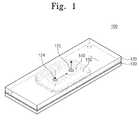
- FIG. 1is a perspective view of a bio-sensor chip according to an embodiment of the present invention
- FIG. 2is an exploded perspective view of a bio-sensor chip according to an embodiment the present invention
- FIG. 3is a perspective view illustrating a cover of a bio-sensor chip according to an embodiment the present invention
- FIG. 4Ais a perspective view illustrating a channel part of a bio-sensor chip according to an embodiment of the present invention.
- FIG. 4Bis a plan view of a mold for manufacturing a channel part of a bio-sensor chip according to an embodiment of the present invention
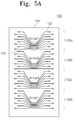
- FIG. 5Ais a plan view illustrating a sensing part of a bio-sensor chip according to an embodiment of the present invention.
- FIG. 5Bis an enlarged plan view illustrating sensors of a bio-sensor chip according to an embodiment of the present invention.
- FIG. 6Ais a perspective view illustrating a board circuit part of a bio-sensor chip according to an embodiment of the present invention.
- FIG. 6Bis an exploded perspective view illustrating a board circuit part of a bio-sensor chip according to an embodiment of the present invention.
- FIG. 6Cis a plan view illustrating an upper chip guide of a board circuit part in a bio-sensor chip according to an embodiment of the present invention.
- FIG. 6Dis a plan view illustrating an upper circuit board of a board circuit part in a bio-sensor chip according to an embodiment of the present invention.
- FIGS. 6E and 6Fare plan views illustrating a lower circuit board of a board circuit part in a bio-sensor chip according to an embodiment of the present invention.
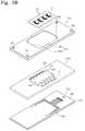
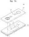
- FIG. 7Ais a perspective view of a bio-sensor chip according to another embodiment of the present invention.
- FIG. 7Bis an exploded perspective view of a bio-sensor chip according to another embodiment of the present invention.
- FIG. 1is a perspective view of a bio-sensor chip according to an embodiment of the present invention.
- a bio-sensor chip 100includes a sensing part 150 , a channel part 140 , a cover 120 , and a board circuit part 130 .
- the sensing part 150senses a target material contained in a solution material introduced from the outside.
- the channel part 140moves the solution material containing the target material into the sensing part 150 .
- the cover 120covers the sensing part 150 and the channel part 140 .
- the board circuit part 130is electrically connected to the sensing part 150 to transmit electrical input/output signals between the sensing part 150 and an external device (e.g., reader).
- the solution material containing the target materialis provided from the outside into the bio-sensor chip 100 through a solution inlet 124 and discharged from the inside of the bio-sensor chip 100 into the outside through a solution outlet 125 .
- the solution material provided inside the bio-sensor chip 100may be provided into the sensing part 150 by the channel part 140 to sense a specific component. Dot-dash arrows of FIG. 1 denote a moving path of the solution material.
- the solution materialmay include a solution diluted with blood, blood serum, or blood plasma.
- FIG. 2is an exploded perspective view of a bio-sensor chip according to an embodiment the present invention.
- the cover 120may be coupled to the board circuit part 130 .
- the cover 120may include coupling protrusions 128 , and coupling grooves 138 into which the coupling protrusions 128 are inserted.
- the cover 120may have a rectangular shape, and the coupling protrusions 128 may be disposed on four edges of the rectangular shape, respectively.
- the board circuit part 130may have a rectangular shape, and the coupling grooves 138 may be defined in four edges of the board circuit part 130 , respectively, so that the coupling grooves 138 are vertically aligned with the coupling protrusions 128 .
- the cover 120is coupled to the board circuit part 130 .
- the sensing part 150 and the channel part 140may be smoothly aligned and disposed between the cover 120 and the board circuit part 130 .
- the sensing part 150 and the sensing part 150may be provided between the cover 120 and the board circuit part 130 .
- the sensing part 150may sense a detection material (target material) of the solution material provided from the outside.
- the channel part 140may provide the solution material containing the target material provided through the solution inlet 124 to the sensing part 150 .
- the sensing part 150may be electrically connected to the board circuit part 130 , and the channel part 140 may be placed on the sensing part 150 .
- the solution materiale.g., the blood may be provided into the channel part 140 through the solution inlet 124
- the bloodmay be provided into the sensing part 150 by the channel part 140 to react to the sensing material contained in the sensing part 150 .
- the bloodis discharged through the solution outlet 125 after the blood reacts to the sensing material.
- FIG. 3is a perspective view illustrating a cover of a bio-sensor chip according to an embodiment the present invention.
- the cover 120may cover the channel part 140 and the sensing part 150 such that the cover 120 may protect the channel part 140 and the sensing part 150 against the outside. Also, the cover 120 may press the channel part 140 at a predetermined pressure to realize a strong coupling between the channel part 140 and the sensing part 150 . Thus, it may prevent the solution material flowing along the channel part 140 from leaking. Accordingly, the cover 120 may have a structure designed to fix positions of the channel part 140 and the sensing part 150 . For example, the cover 120 may have a structure that may provide a space 126 into which the whole channel part 140 or an upper portion of the channel part 140 may be inserted and a space 127 into which the sensing part 150 may be inserted. The space 127 may further include a space for protecting a wire bonding for electrically connecting the sensing part 150 to the board circuit part 130 . These spaces 126 and 127 may be defined by an engraved pattern.
- a body 121 of the cover 120may be formed of a transparent material to easily observe a flow state or leak state of the solution material, an alignment state between the sensing part 150 and the channel part 140 , an electrical connection state between the sensing part 150 and the board circuit part 130 , etc.
- the transparent material constituting the body 121 of the cover 120may include a transparent plastic such as polymethylmethacrylate (hereinafter, referred to as a “PMMA”).
- the PMMAis a kind of thermoplastic acryl resins and is widely used as a substitute of glass.
- the PMMAis generally easy to handle and inexpensive.
- the PMMAis a thermoplastic material, it may be easily manufactured to a desired shape. That is, when a pressure is applied to the heated PMMA disposed on a metal mold, a plastic pattern having a shape opposite to that of the mold may be formed.
- the transparent material constituting the body 121 of the cover 120may include one of polycarbonate, cyclic olefine copolymer, polyethylene sulfone, polystyrene, and combinations thereof.
- the solution inlet 124 and the solution outlet 125may be provided in the cover 120 .
- the solution inlet 124 and the solution outlet 125may pass through the body 121 of the cover 120 and have vertically opened shapes, respectively.
- FIG. 4Ais a perspective view illustrating a channel part of a bio-sensor chip according to an embodiment of the present invention
- FIG. 4Bis a plan view of a mold for manufacturing a channel part of a bio-sensor chip according to an embodiment of the present invention
- the channel part 140may guide the solution material such that the solution material flows through a desired path.
- the channel part 140includes a fluid channel 143 , a channel solution inlet 144 , and a channel solution outlet 145 .
- the fluid channel 143provides a path through which the solution material flows.
- the channel solution inlet 144is provided at one end of the fluid channel 143 to provide a path through which the solution material provided into the fluid channel 143 is introduced.
- the channel solution outlet 145provides a path through which the solution material passing through the fluid channel 143 is discharged.
- the fluid channel 143 , the channel solution inlet 144 , and the channel solution outlet 145are formed in the body 141 to define the channel part 140 .
- the channel solution inlet 144 and the channel solution outlet 145may pass through the body 141 and have vertically opened shapes, respectively.
- the channel solution inlet 144 and the channel solution outlet 145may be vertically aligned with the solution inlet 124 and the solution outlet 125 , respectively.
- the channel solution inlet 144 and the channel solution outlet 145may have the same size as the solution inlet 124 and the solution outlet 125 , respectively. As a result, the solution material may smoothly flow between the cover 120 and the channel part 140 .
- the channel part 140is in contact with the sensing part 150 disposed below thereof and may be pressed at a predetermined force by the cover 120 disposed over thereof to prevent the solution material flowing into the fluid channel 143 from leaking.
- the body 141 of the channel part 140may have elasticity and be formed of a transparent material, e.g., polydimethylsiloxane (hereinafter, referred to as a “PDMS”) to easily observe a flow state or leak state of the solution material and an alignment state between the sensing part 150 and the channel part 140 .
- the PDMSmay be a silicon-based organic polymer widely used as a medical appliance such as a contact lens and include a bio-compatible material.
- a mold 146 having a shape opposite to a desired shapemay be firstly manufactured to form the channel part 140 .
- a pattern 148e.g., an Su-8 pattern (a pattern by using Su-8 photoresist commercially available from Microchem Company which is applied as a negative-type photoresist in order to form a microstructure) may be formed on a 4-inch silicon wafer 147 using a MEMS process to manufacture the PDMS mold 146 .
- the channel part 140may be mass producible.
- a cross-section of the fluid channel 143may affect a flow speed of the solution material and also affect a volume interacting with the sensing part 150 per unit volume in the total flow amount of the solution material.
- the cross-section of the fluid channel 143may be designed in a suitable size in which a target molecule (the target material) may interact with a probe molecule (the sensing material).
- the fluid channel 143may have a tetragonal shape (e.g., a rectangular shape) in section and may be restrictively disposed on a lower portion of the body 141 that is in contact with the sensing part 150 .
- FIG. 5Ais a plan view illustrating a sensing part of a bio-sensor chip according to an embodiment of the present invention
- FIG. 5Bis an enlarged plan view illustrating sensors of a bio-sensor chip according to an embodiment of the present invention.
- the sensing part 150may include a plurality of sensors 152 on a semiconductor substrate 151 .
- the sensing part 150may have a size of approximately 15 mm ⁇ 25 mm.
- the solution material provided through the channel solution inlet 144 of the channel part 140is guided by the fluid channel 143 to pass through the sensors 152 .
- the sensors 152may detect the target material in the flowing solution material.
- the semiconductor substrate 151may include a silicon-on-insulator (SOI) substrate.
- the sensors 152may be designed to detect target materials different from each other.
- the sensors 152may be divided into a plurality of groups, e.g., a first group 152 a , a second group 152 b , and a third group 152 c , and a fourth group 152 d .
- the first to third groups 152 a to 152 cmay independently detect three different types of protein markers, and the fourth group 152 d may obtain a reference signal of an electrical signal change of the sensing part 150 .
- Each of the four groups 152 a to 152 dmay include, e.g., eight sensors 152 .
- FIG. 5Bis a view of a portion 153 of the sensors 152 .
- each of the sensors 152may include a silicon nano-wire.
- each of the sensors 152may include a nano-channel 154 and a source/drain 155 disposed at both sides of the nano-channel 154 .
- the nano-channel 154may have a height within the range of several ten nm (a thickness of the semiconductor substrate 151 ).
- the nano-channel 154may be formed of silicon doped with a P-type or an N-type dopant.
- An antibody (sensing material) specifically coupled to the marker (detection material) to be detectedmay be fixed to a surface of the nano-channel 154 through a bio-surface reaction.
- the sensors 152 of the respective groups 152 a to 152 dmay have the same channel width W and length L as each other.
- the nano-channel 154may have the width W within the range of several ten nm to several hundred nm and the length L within the range of about 2 to about 20 nm.
- the source/drain 155may be formed of a metal electrode such as Au, Au/Cr, Au/Ti, and Au/Cr/Al. An external voltage may be applied to the nano-channel 154 through the source/drain 155 .
- the sensors 150may be configured as disclosed in U.S. Pat. No. 6,870,235, or U.S. Published Patent Application No. 2006/0054936, the entire contents of which are hereby incorporated by reference.
- FIG. 6Ais a perspective view illustrating a board circuit part of a bio-sensor chip according to an embodiment of the present invention
- FIG. 6Bis an exploded perspective view illustrating a board circuit part of a bio-sensor chip according to an embodiment of the present invention.
- the board circuit part 130may provide a place in which the sensing part 150 is packaged.
- the board circuit part 130may input/output the electrical signal generated in the sensing part 150 .
- the board circuit part 130may be configured to be compatible with an external device such as the reader.
- the board circuit part 130may include a printed circuit board 131 having a substantially rectangular shape with a size of a slide glass, i.e., a size of about 76 mm ⁇ 25 mm.
- a glass fiber including an epoxy resinmay be folded over and over again to manufacture the printed circuit board 131 .
- the printed circuit board 131may have elasticity and a characteristic having a certain degree of flexibility such that a compressive force is not concentrated at the sensing part 150 but dispersed when the printed circuit board 131 is coupled to the cover 120 for packaging.
- the coupling grooves 138 into which the coupling protrusions 128 are insertedmay be defined in four edges of the printed circuit board 131 , respectively.
- the printed circuit board 131may include internal connection pads 132 and 134 electrically connected to the sensing part 150 , and a guide groove 135 exposing the internal connection pads 132 and 134 and guiding an alignment position of the sensing part 150 .
- the printed circuit board 131may have a single layer structure using one layer or a multilayer structure in which several layers are folded over and over again. According to the embodiment of the present invention, the printed circuit board 131 may have the multilayer structure as described later with reference to FIGS. 6C to 6F .
- the printed circuit board 131may have the multilayer structure including an upper chip guide 131 a guiding the sensing part 150 in position, and circuit boards 131 b and 131 c on which electrical circuits are disposed.
- the circuit boards 131 b and 131 cmay include an upper circuit board 131 b electrically connected to the sensing part 150 and a lower circuit board 131 c electrically connected to the external device, e.g., the reader.
- FIG. 6Cis a plan view illustrating an upper chip guide of a board circuit part in a bio-sensor chip according to an embodiment of the present invention
- FIG. 6Dis a plan view illustrating an upper circuit board of a board circuit part in a bio-sensor chip according to an embodiment of the present invention
- FIGS. 6E and 6 Fare plan views illustrating a lower circuit board of a board circuit part in a bio-sensor chip according to an embodiment of the present invention.
- the upper chip guide 131 amay include the coupling grooves 138 defined in the four edges thereof and a guide groove 135 guiding the sensing part 150 in position.
- the guide groove 135may include a first groove 135 a for exposing a back substrate bias pad 132 and a second groove 135 b for exposing a bonding pad 134 .
- the upper circuit board 131 bmay include the internal connection pads 132 and 134 electrically connected to the sensing part 150 .
- the internal connection pads 132 and 134may include the back substrate bias pad 132 and the bonding pad 134 .
- a bonding wire 139may have one end and the other end that are formed of Au and electrically connected to the sensing part 150 and the bonding pad 134 , respectively.
- the internal connection pads 132 and 134may be formed of a copper foil. A gold foil may be further coated on a surface of the bonding pad 134 .
- a conductive double-sided adhesive carbon tapemay be inserted between the semiconductor substrate 151 and the back substrate bias pad 132 .
- one back substrate bias pad 132may be provided, and four pairs of bonding pads 134 may be provided.
- the four pairs of bonding pads 134may correspond to the four groups (reference numeral 152 a to 152 d of FIG. 5A ) of the sensing part 150 .
- a pair of bonding pads 134may be electrically connected to the sensors 152 included in the one group 152 a by the bonding wire 139 .
- the number of pads 132 and 134is not limited to the above-described number of pads. For example, the larger or smaller number of pads 132 and 134 may be provided.
- the lower circuit board 131 cmay include a first layer 136 including a plurality of electrical interconnections 161 and a second layer 137 including a plurality of external connection pads 162 electrically connected to the plurality of electrical interconnections 161 .
- the circuit board 131 c and 131 dmay include three layers, i.e., the upper circuit board 131 b constituting the highest layer, the first layer 136 constituting a middle layer, and the second layer 137 constituting the lowest layer.
- the first layer 136may include total nine electrical interconnections 161 including four pairs of first interconnections 161 a electrically connected to the four pairs of bonding pads 134 and one second interconnection 161 b electrically connected to the back substrate bias pad 132 .
- the number of electrical interconnections 161is not limited to the above-described number of interconnections. For example, the larger or smaller number of electrical interconnections 161 may be provided.
- the electrical interconnections 161may be formed of a copper foil. Since the first layer 136 is disposed between the upper circuit board 131 b and the second layer 137 , the plurality of electrical interconnections 161 disposed on the first layer 136 may be protected against external contact or the solution material.
- the second layer 137may include nine external connection pads 162 electrically connected to the nine electrical interconnections 161 .
- the number of external connection pads 162is not limited to the above-described number. For example, the larger or smaller number of external connection pads 162 may be provided.
- the external connection pads 162may be electrically connected to the external device such as the reader. Thus, the electrical signal of the sensing part 150 may be transmitted to the reader.
- the external connection pads 162may be formed of a copper foil. A gold foil may be coated on surfaces of the external connection pads 162 .
- a plurality of holes 163 for passing through the first and second layers 136 and 137may be provided to be socket-coupled to the reader.
- a metalsuch as Cu, Au, or Cu/Au may be coated on an inner wall of each of the holes 163 .
- FIG. 7Ais a perspective view of a bio-sensor chip according to another embodiment of the present invention.
- a bio-sensor chip 200includes an upper cover 110 , a lower cover 120 , and a board circuit part 130 .
- a solution material containing a target materialis introduced and discharged from/into the outside through the upper cover 110 .
- the lower cover 120covers a sensing part 150 for sensing the introduced solution material and a channel part 140 for moving the solution material to the sensing part 150 .
- the board circuit part 130transmits an electrical input/output signal between the sensing part 150 and an external device (e.g., reader).
- the upper cover 110 and the lower cover 120may be manufactured as separate structures to form two-layer structure. Alternatively, the upper cover 110 and the lower cover 120 may be integrated in one body to form a single-layer structure.
- the bio-sensor chip 200may include a provision part 119 for providing the solution material from the outside and receiving the solution material in which the detection process (sensing process) has been performed to store the solution material.
- the provision part 119may be disposed in the upper cover 110 .
- FIG. 7Bis an exploded perspective view of a bio-sensor chip according to another embodiment of the present invention.
- the upper cover 110may include the provision part 119 for providing the solution material.
- the provision part 119may include solution flow channels 113 a and 113 b for providing moving paths of the solution material, an upper solution inlet 114 for injecting the solution material, and an upper solution outlet 115 for discharging the solution material.
- a filter 116 for separating a specific component of the solution materialmay be disposed at one end of the first solution flow channel 113 a .
- a storage container 117 for storing the solution material for which the detection process is already completedmay be disposed at one end of the second solution flow channel 113 b.
- the filter 116may filter blood corpuscle of whole blood to separate blood plasma or blood serum from the blood.
- the filter 116may include a paper filter, e.g., a paper filter commercialized as the model name “MDI-FRI”.
- MDI-FRIa paper filter commercialized as the model name “MDI-FRI”.
- the bloodmay be absorbed into the filter 116 to remove blood corpuscle components such as red blood cells, white blood cells, and blood platelets.
- the blood plasma or the blood serum in which the blood corpuscle components of the whole blood are removedmay pass through the first solution flow channel 113 a .
- the blood containing a target material to be detectedmay reach the upper solution inlet 114 by a capillary action, and then the blood passing through the upper solution inlet 114 may be provided into the sensing part 150 via the channel part 140 to detect the specific component of the blood.
- a body 111 of the upper cover 110may be formed of a transparent material to easily observe a leak state of the solution material from the outside.
- the body 111 of the upper cover 110may be formed of one of polymethylmethacrylate, polycarbonate, cyclic olefine copolymer, polyethylene sulfone, polystyrene, and combinations thereof.
- the lower cover 120 , the channel part 140 , the sensing part 150 , and the board circuit part 130may have the substantially same structure as those described with reference to FIGS. 1 through 6F . Roughly explaining, the lower cover 120 and the board circuit part 130 may be inserted into the coupling groove 138 , and thus coupled to each other. The channel part 140 and the sensing part 150 may be packaged between the lower cover 120 and the board circuit part 130 , which are coupled to each other.
- the lower cover 120may include a solution inlet 124 (hereinafter, referred to as a lower solution inlet) vertically aligned with the upper solution inlet 114 and a solution outlet 125 (hereinafter, referred to as a lower solution outlet) vertically aligned with the upper solution outlet 115 .
- the channel part 140may include a channel solution inlet 144 vertically aligned with the lower solution inlet 124 , a channel solution outlet 145 vertically aligned with the lower solution outlet 125 , and a fluid channel 143 disposed between the channel inletsolution inlet 144 and the channel solution outlet 145 to guide the solution material such that the solution material crossly flows through sensors 152 of the sensing part 150 .
- the board circuit part 130may include a printed circuit board 131 on which an electrical circuit coupled to external devices such as a back substrate bias pad 132 , a bonding pad 134 , and a reader is disposed.
- the bio-sensor chip 200may easily separate the blood corpuscle and the blood plasma (or the blood serum) from the blood using the filter 116 without employing a centrifugal separator.
- the bloodmay sequentially flow through the upper solution inlet 114 , the lower solution inlet 124 , and the channel solution inlet 114 to flow into the fluid channel 143 . That is, the blood may be moved into the sensing part 150 due to the capillary action without employing a syringe pump.
- the target materialinteracts with a detection material to cause a change of conductivity. As a result, the existence or concentration of the target material may be detected.
- the blood for which the detection process is already completedmay sequentially discharged through the channel solution outlet 145 , the lower solution outlet 125 , and the upper solution outlet 115 .
- the discharged bloodmay flow into the storage container 117 through the second solution flow channel 113 b.
- the bio-sensor chip according to the embodiment of the present inventionhas a simple manufacturing process, relatively low manufacturing costs, and easy portability.
- the bio-sensor chipcan simple detect the target material.
- the bio-sensorcan be easily used for the medical profession such as a hospital as well as a home.
- the bio-sensor chipitself can filter the solution material to separate the target material.
- the solution materialcan be easily separated without employing a device such as the centrifugal separator.
- a devicesuch as the syringe pump may be not required to maximize the portability and usability of the bio-sensor chip.
- the embodiment of the present inventioncan be applied to the semiconductor industry and manufacturing industry for manufacturing bio-sensor chips or medical devices and other health devices.
Landscapes
- Chemical & Material Sciences (AREA)
- Health & Medical Sciences (AREA)
- Life Sciences & Earth Sciences (AREA)
- Analytical Chemistry (AREA)
- General Health & Medical Sciences (AREA)
- Chemical Kinetics & Catalysis (AREA)
- Physics & Mathematics (AREA)
- Molecular Biology (AREA)
- Engineering & Computer Science (AREA)
- Microelectronics & Electronic Packaging (AREA)
- Clinical Laboratory Science (AREA)
- Hematology (AREA)
- Electrochemistry (AREA)
- Dispersion Chemistry (AREA)
- Biochemistry (AREA)
- General Physics & Mathematics (AREA)
- Immunology (AREA)
- Pathology (AREA)
- Nanotechnology (AREA)
- Spectroscopy & Molecular Physics (AREA)
- Investigating Or Analyzing Materials By The Use Of Electric Means (AREA)
- Apparatus Associated With Microorganisms And Enzymes (AREA)
Abstract
Description
Claims (20)
Applications Claiming Priority (4)
| Application Number | Priority Date | Filing Date | Title |
|---|---|---|---|
| KR1020080120189AKR101173981B1 (en) | 2008-11-29 | 2008-11-29 | Bio sensor |
| KR10-2008-0120189 | 2008-11-29 | ||
| KR1020080130964AKR101179555B1 (en) | 2008-12-22 | 2008-12-22 | Bio-sensor chip |
| KR10-2008-0130964 | 2008-12-22 |
Publications (2)
| Publication Number | Publication Date |
|---|---|
| US20100133510A1 US20100133510A1 (en) | 2010-06-03 |
| US8169006B2true US8169006B2 (en) | 2012-05-01 |
Family
ID=42221936
Family Applications (1)
| Application Number | Title | Priority Date | Filing Date |
|---|---|---|---|
| US12/561,032Expired - Fee RelatedUS8169006B2 (en) | 2008-11-29 | 2009-09-16 | Bio-sensor chip for detecting target material |
Country Status (2)
| Country | Link |
|---|---|
| US (1) | US8169006B2 (en) |
| JP (2) | JP5586921B2 (en) |
Cited By (6)
| Publication number | Priority date | Publication date | Assignee | Title |
|---|---|---|---|---|
| US9012255B1 (en)* | 2010-10-27 | 2015-04-21 | Dunan Microstaq, Inc. | MEMS package |
| US10126263B2 (en) | 2012-10-16 | 2018-11-13 | Koninklijke Philips N.V. | Wide dynamic range fluid sensor based on nanowire platform |
| US10124340B2 (en) | 2015-12-08 | 2018-11-13 | Electronics And Telecommunications Research Institute | Reagent storage device and bio-reaction apparatus including the same |
| US10473648B2 (en) | 2017-01-02 | 2019-11-12 | Electronics And Telecommunications Research Institute | Biosensor |
| US10932695B2 (en) | 2012-09-17 | 2021-03-02 | Verily Life Sciences Llc | Sensing system |
| US12036028B2 (en) | 2020-06-22 | 2024-07-16 | Electronics And Telecommunications Research Institute | Bio-signal detection and stimulation device |
Families Citing this family (85)
| Publication number | Priority date | Publication date | Assignee | Title |
|---|---|---|---|---|
| US20110312078A1 (en)* | 2010-06-17 | 2011-12-22 | Geneasys Pty Ltd | Microfluidic device for detecting target nucleic acid sequences in mitochondrial dna |
| CN105149023B (en)* | 2010-06-30 | 2018-06-12 | 安派科生物医学科技有限公司 | disease detection instrument |
| CN102033089A (en)* | 2010-10-27 | 2011-04-27 | 清华大学 | Biosensor and packaging structure thereof and detection system |
| CN202401049U (en)* | 2011-01-10 | 2012-08-29 | 伊鲁米那股份有限公司 | Clamp plate and system for reagent storage and transfer |
| US8951781B2 (en) | 2011-01-10 | 2015-02-10 | Illumina, Inc. | Systems, methods, and apparatuses to image a sample for biological or chemical analysis |
| GB2489504A (en)* | 2011-03-31 | 2012-10-03 | Sapient Sensors | A device for identifying the presence of a specific target molecule or biomarker by sensing an electrical property |
| KR101464028B1 (en)* | 2011-09-20 | 2014-12-04 | 주식회사 세라젬메디시스 | Module type biosensor |
| TWI618932B (en)* | 2012-03-08 | 2018-03-21 | 上海新申派科技有限公司 | Micro-devices for improved disease detection |
| GB2500658A (en)* | 2012-03-28 | 2013-10-02 | Dna Electronics Ltd | Biosensor device and system |
| US8798332B2 (en) | 2012-05-15 | 2014-08-05 | Google Inc. | Contact lenses |
| US9158133B1 (en) | 2012-07-26 | 2015-10-13 | Google Inc. | Contact lens employing optical signals for power and/or communication |
| US8857981B2 (en) | 2012-07-26 | 2014-10-14 | Google Inc. | Facilitation of contact lenses with capacitive sensors |
| US9523865B2 (en) | 2012-07-26 | 2016-12-20 | Verily Life Sciences Llc | Contact lenses with hybrid power sources |
| US9298020B1 (en) | 2012-07-26 | 2016-03-29 | Verily Life Sciences Llc | Input system |
| JP6347780B2 (en)* | 2012-07-30 | 2018-06-27 | ザ リージェンツ オブ ザ ユニバーシティ オブ カリフォルニア | Biomolecule detection test strip design |
| US8919953B1 (en) | 2012-08-02 | 2014-12-30 | Google Inc. | Actuatable contact lenses |
| US8971978B2 (en) | 2012-08-21 | 2015-03-03 | Google Inc. | Contact lens with integrated pulse oximeter |
| US9696564B1 (en) | 2012-08-21 | 2017-07-04 | Verily Life Sciences Llc | Contact lens with metal portion and polymer layer having indentations |
| US9111473B1 (en) | 2012-08-24 | 2015-08-18 | Google Inc. | Input system |
| US8820934B1 (en) | 2012-09-05 | 2014-09-02 | Google Inc. | Passive surface acoustic wave communication |
| US20140192315A1 (en) | 2012-09-07 | 2014-07-10 | Google Inc. | In-situ tear sample collection and testing using a contact lens |
| US9398868B1 (en) | 2012-09-11 | 2016-07-26 | Verily Life Sciences Llc | Cancellation of a baseline current signal via current subtraction within a linear relaxation oscillator-based current-to-frequency converter circuit |
| US9326710B1 (en) | 2012-09-20 | 2016-05-03 | Verily Life Sciences Llc | Contact lenses having sensors with adjustable sensitivity |
| US8870370B1 (en) | 2012-09-24 | 2014-10-28 | Google Inc. | Contact lens that facilitates antenna communication via sensor impedance modulation |
| US8960898B1 (en) | 2012-09-24 | 2015-02-24 | Google Inc. | Contact lens that restricts incoming light to the eye |
| US8979271B2 (en) | 2012-09-25 | 2015-03-17 | Google Inc. | Facilitation of temperature compensation for contact lens sensors and temperature sensing |
| US20140088372A1 (en) | 2012-09-25 | 2014-03-27 | Google Inc. | Information processing method |
| US8989834B2 (en) | 2012-09-25 | 2015-03-24 | Google Inc. | Wearable device |
| US8960899B2 (en) | 2012-09-26 | 2015-02-24 | Google Inc. | Assembling thin silicon chips on a contact lens |
| US9884180B1 (en) | 2012-09-26 | 2018-02-06 | Verily Life Sciences Llc | Power transducer for a retinal implant using a contact lens |
| US8821811B2 (en) | 2012-09-26 | 2014-09-02 | Google Inc. | In-vitro contact lens testing |
| US8985763B1 (en) | 2012-09-26 | 2015-03-24 | Google Inc. | Contact lens having an uneven embedded substrate and method of manufacture |
| US9063351B1 (en) | 2012-09-28 | 2015-06-23 | Google Inc. | Input detection system |
| US8965478B2 (en) | 2012-10-12 | 2015-02-24 | Google Inc. | Microelectrodes in an ophthalmic electrochemical sensor |
| US9176332B1 (en) | 2012-10-24 | 2015-11-03 | Google Inc. | Contact lens and method of manufacture to improve sensor sensitivity |
| US9757056B1 (en) | 2012-10-26 | 2017-09-12 | Verily Life Sciences Llc | Over-molding of sensor apparatus in eye-mountable device |
| US8874182B2 (en) | 2013-01-15 | 2014-10-28 | Google Inc. | Encapsulated electronics |
| US9289954B2 (en) | 2013-01-17 | 2016-03-22 | Verily Life Sciences Llc | Method of ring-shaped structure placement in an eye-mountable device |
| US20140209481A1 (en) | 2013-01-25 | 2014-07-31 | Google Inc. | Standby Biasing Of Electrochemical Sensor To Reduce Sensor Stabilization Time During Measurement |
| US9636016B1 (en) | 2013-01-25 | 2017-05-02 | Verily Life Sciences Llc | Eye-mountable devices and methods for accurately placing a flexible ring containing electronics in eye-mountable devices |
| US9161712B2 (en) | 2013-03-26 | 2015-10-20 | Google Inc. | Systems and methods for encapsulating electronics in a mountable device |
| US9113829B2 (en) | 2013-03-27 | 2015-08-25 | Google Inc. | Systems and methods for encapsulating electronics in a mountable device |
| US20140371560A1 (en) | 2013-06-14 | 2014-12-18 | Google Inc. | Body-Mountable Devices and Methods for Embedding a Structure in a Body-Mountable Device |
| US9084561B2 (en) | 2013-06-17 | 2015-07-21 | Google Inc. | Symmetrically arranged sensor electrodes in an ophthalmic electrochemical sensor |
| US9948895B1 (en) | 2013-06-18 | 2018-04-17 | Verily Life Sciences Llc | Fully integrated pinhole camera for eye-mountable imaging system |
| US9685689B1 (en) | 2013-06-27 | 2017-06-20 | Verily Life Sciences Llc | Fabrication methods for bio-compatible devices |
| US9028772B2 (en) | 2013-06-28 | 2015-05-12 | Google Inc. | Methods for forming a channel through a polymer layer using one or more photoresist layers |
| US9492118B1 (en) | 2013-06-28 | 2016-11-15 | Life Sciences Llc | Pre-treatment process for electrochemical amperometric sensor |
| US9307901B1 (en) | 2013-06-28 | 2016-04-12 | Verily Life Sciences Llc | Methods for leaving a channel in a polymer layer using a cross-linked polymer plug |
| US9814387B2 (en) | 2013-06-28 | 2017-11-14 | Verily Life Sciences, LLC | Device identification |
| US9572522B2 (en) | 2013-12-20 | 2017-02-21 | Verily Life Sciences Llc | Tear fluid conductivity sensor |
| US9654674B1 (en) | 2013-12-20 | 2017-05-16 | Verily Life Sciences Llc | Image sensor with a plurality of light channels |
| EP2907572A1 (en)* | 2014-02-12 | 2015-08-19 | Tethis S.p.A. | Device for preparing a substrate for processing samples |
| US9366570B1 (en) | 2014-03-10 | 2016-06-14 | Verily Life Sciences Llc | Photodiode operable in photoconductive mode and photovoltaic mode |
| US9184698B1 (en) | 2014-03-11 | 2015-11-10 | Google Inc. | Reference frequency from ambient light signal |
| US10634590B2 (en)* | 2014-03-11 | 2020-04-28 | Emd Millipore Corporation | IHC, tissue slide fluid exchange disposable and system |
| US9789655B1 (en) | 2014-03-14 | 2017-10-17 | Verily Life Sciences Llc | Methods for mold release of body-mountable devices including microelectronics |
| US20160054312A1 (en) | 2014-04-28 | 2016-02-25 | Nanomedical Diagnostics, Inc. | Chemically differentiated sensor array |
| US11215580B2 (en) | 2014-04-28 | 2022-01-04 | Cardea Bio, Inc. | System and method for DNA sequencing and blood chemistry analysis |
| US9618476B2 (en)* | 2014-04-28 | 2017-04-11 | Nanomedical Diagnostics, Inc. | System and method for electronic biological sample analysis |
| US20180299403A1 (en)* | 2014-11-07 | 2018-10-18 | Proteosense | Devices, systems, and methods for the detection of analytes |
| US11782057B2 (en) | 2014-12-18 | 2023-10-10 | Cardea Bio, Inc. | Ic with graphene fet sensor array patterned in layers above circuitry formed in a silicon based cmos wafer |
| US10006910B2 (en) | 2014-12-18 | 2018-06-26 | Agilome, Inc. | Chemically-sensitive field effect transistors, systems, and methods for manufacturing and using the same |
| US11921112B2 (en) | 2014-12-18 | 2024-03-05 | Paragraf Usa Inc. | Chemically-sensitive field effect transistors, systems, and methods for manufacturing and using the same |
| US9618474B2 (en) | 2014-12-18 | 2017-04-11 | Edico Genome, Inc. | Graphene FET devices, systems, and methods of using the same for sequencing nucleic acids |
| US12298301B2 (en) | 2014-12-18 | 2025-05-13 | Cardea Bio, Inc. | Chemically-sensitive field effect transistors, systems, and methods for manufacturing and using the same |
| US10408825B2 (en) | 2015-05-19 | 2019-09-10 | Electronics And Telecommunications Research Institute | Biosensor |
| EP3936863A1 (en) | 2016-03-21 | 2022-01-12 | Nooma Bio, Inc. | Wafer-scale assembly of insulator-membrane-insulator devices for nanopore sensing |
| CA3067304C (en) | 2016-06-18 | 2024-05-07 | Graphwear Technologies Inc. | Polar fluid gated field effect devices |
| WO2017216641A2 (en)* | 2016-06-18 | 2017-12-21 | Graphwear Technologies Inc. | Polar fluid gated field effect devices |
| KR101838966B1 (en)* | 2016-08-16 | 2018-03-15 | 포항공과대학교 산학협력단 | Multi-sensor of nano-floating structure and manufacturing method thereof |
| US10710068B2 (en)* | 2017-09-20 | 2020-07-14 | e-SENSE, Inc. | Microfluidic chip with chemical sensor having back-side contacts |
| FR3074489B1 (en)* | 2017-12-05 | 2023-04-21 | Centre Nat Rech Scient | NANOSTRUCTURE PLATFORM FOR CELLULAR INTERFACING AND CORRESPONDING FABRICATION METHOD |
| CN108241240B (en)* | 2018-02-08 | 2021-05-14 | 上海天马微电子有限公司 | A display panel and display device |
| JP6739121B2 (en)* | 2018-04-19 | 2020-08-12 | ティーイーアイソリューションズ株式会社 | Analysis equipment |
| JP7485656B2 (en) | 2018-05-18 | 2024-05-16 | リプリーヴ カーディオヴァスキュラー インコーポレイテッド | Method and system for treating acute decompensated heart failure |
| US11561197B2 (en) | 2018-06-29 | 2023-01-24 | AMMR Joint Venture | Electronic detection of a target based on enzymatic cleavage of a reporter moiety |
| US12290380B1 (en) | 2018-08-20 | 2025-05-06 | Reprieve Cardiovascular, Inc. | Method and system to monitor urine output and manage fluid retention in a patient |
| TWI853851B (en) | 2018-11-15 | 2024-09-01 | 中國商深圳華大智造科技有限公司 | Microfluidic apparatus and method of making |
| US20220291192A1 (en)* | 2019-09-25 | 2022-09-15 | Roche Sequencing Solutions, Inc. | Interface for automated fluid injection |
| US20230417667A1 (en)* | 2020-11-03 | 2023-12-28 | The General Hospital Corporation | Sensor-chip and manufacturing method thereof |
| US12303271B2 (en) | 2021-04-15 | 2025-05-20 | Reprieve Cardiovascular, Inc. | Urine collection systems and associated methods and devices |
| EP4330665A1 (en)* | 2021-04-26 | 2024-03-06 | Reprieve Cardiovascular, Inc. | Measuring and/or detecting analytes in urine, and associated systems, devices, and methods |
| EP4539989A4 (en)* | 2022-06-17 | 2025-08-27 | Siemens Healthcare Diagnostics Inc | ACUSTOPHORESIS DEVICES WITH CONDUCTIVE ELECTRODES AND METHODS |
| US20250082264A1 (en) | 2023-09-12 | 2025-03-13 | Reprieve Cardiovascular, Inc. | Fluid therapy based on adjusted urine output rate, and associated systems, devices, and methods |
Citations (21)
| Publication number | Priority date | Publication date | Assignee | Title |
|---|---|---|---|---|
| US4064552A (en)* | 1976-02-03 | 1977-12-20 | Angelucci Thomas L | Multilayer flexible printed circuit tape |
| JPH03122558A (en) | 1989-10-04 | 1991-05-24 | Olympus Optical Co Ltd | Sensor structure and manufacture thereof |
| JPH03293547A (en) | 1990-04-12 | 1991-12-25 | Olympus Optical Co Ltd | Semiconductor sensor apparatus |
| US5096669A (en) | 1988-09-15 | 1992-03-17 | I-Stat Corporation | Disposable sensing device for real time fluid analysis |
| JP3122558B2 (en) | 1993-07-19 | 2001-01-09 | シャープ株式会社 | Multicolor light emitting diode unit |
| JP2001281198A (en) | 2000-03-28 | 2001-10-10 | Nec Corp | Apparatus and method for measuring liquid sample |
| US6331257B1 (en)* | 1998-05-15 | 2001-12-18 | Hughes Electronics Corporation | Fabrication of broadband surface-micromachined micro-electro-mechanical switches for microwave and millimeter-wave applications |
| JP3293547B2 (en) | 1998-02-10 | 2002-06-17 | 富士ゼロックス株式会社 | Image forming method and recording medium used therefor |
| WO2002048701A2 (en) | 2000-12-11 | 2002-06-20 | President And Fellows Of Harvard College | Nanosensors |
| WO2003061569A2 (en) | 2002-01-18 | 2003-07-31 | Cholestech Corporation | High-density lipoprotein assay device and method |
| WO2005000114A2 (en) | 2003-06-03 | 2005-01-06 | Bayer Healthcare Llc | Portable medical diagnostic apparatus |
| KR100466541B1 (en) | 2002-10-09 | 2005-01-15 | 한국전자통신연구원 | Apparatus for transporting micro-fluids |
| US6870235B2 (en) | 2002-05-15 | 2005-03-22 | Fujitsu Limited | Silicon-on-insulator biosensor device |
| KR100550515B1 (en) | 2003-12-26 | 2006-02-10 | 한국전자통신연구원 | Biomolecular Filter and Manufacturing Method Thereof |
| US7025774B2 (en)* | 2001-06-12 | 2006-04-11 | Pelikan Technologies, Inc. | Tissue penetration device |
| WO2006126487A1 (en) | 2005-05-23 | 2006-11-30 | Cybox Co., Ltd | Microchip and method of producing microchip |
| US20070026645A1 (en)* | 2000-08-22 | 2007-02-01 | President And Fellows Of Harvard College | Doped elongated semiconductors, growing such semiconductors, devices including such semiconductors, and fabricating such devices |
| US7177161B2 (en)* | 2003-09-05 | 2007-02-13 | Seiko Epson Corporation | Compact radio equipment and method of mounting the same |
| KR20070039335A (en) | 2005-10-07 | 2007-04-11 | 케이맥(주) | Bio-sensor chip of having multi-channel |
| KR20070099233A (en) | 2006-04-04 | 2007-10-09 | 주식회사 올메디쿠스 | Biosensor chip with non-powered blood separation means |
| WO2008087799A1 (en) | 2007-01-18 | 2008-07-24 | Konica Minolta Opto, Inc. | Microchip and method for manufacturing the microchip |
Family Cites Families (3)
| Publication number | Priority date | Publication date | Assignee | Title |
|---|---|---|---|---|
| JP2694809B2 (en)* | 1994-12-14 | 1997-12-24 | 日本電気株式会社 | Enzyme immunoassay method and enzyme immunosensor |
| JP2005172773A (en)* | 2003-12-05 | 2005-06-30 | Mari Tabuchi | Substrate for electrophoresis, and biological test sample analyzing device and method |
| US20100248209A1 (en)* | 2006-06-30 | 2010-09-30 | Suman Datta | Three-dimensional integrated circuit for analyte detection |
- 2009
- 2009-09-16USUS12/561,032patent/US8169006B2/ennot_activeExpired - Fee Related
- 2009-11-05JPJP2009254130Apatent/JP5586921B2/ennot_activeExpired - Fee Related
- 2011
- 2011-12-02JPJP2011264813Apatent/JP2012088326A/ennot_activeCeased
Patent Citations (27)
| Publication number | Priority date | Publication date | Assignee | Title |
|---|---|---|---|---|
| US4064552A (en)* | 1976-02-03 | 1977-12-20 | Angelucci Thomas L | Multilayer flexible printed circuit tape |
| US5096669A (en) | 1988-09-15 | 1992-03-17 | I-Stat Corporation | Disposable sensing device for real time fluid analysis |
| JPH03122558A (en) | 1989-10-04 | 1991-05-24 | Olympus Optical Co Ltd | Sensor structure and manufacture thereof |
| JPH03293547A (en) | 1990-04-12 | 1991-12-25 | Olympus Optical Co Ltd | Semiconductor sensor apparatus |
| JP3122558B2 (en) | 1993-07-19 | 2001-01-09 | シャープ株式会社 | Multicolor light emitting diode unit |
| JP3293547B2 (en) | 1998-02-10 | 2002-06-17 | 富士ゼロックス株式会社 | Image forming method and recording medium used therefor |
| US6331257B1 (en)* | 1998-05-15 | 2001-12-18 | Hughes Electronics Corporation | Fabrication of broadband surface-micromachined micro-electro-mechanical switches for microwave and millimeter-wave applications |
| US6709856B2 (en) | 2000-03-28 | 2004-03-23 | Nec Corporation | Liquid sample measuring device containing electrode sensor with enzyme layer |
| JP2001281198A (en) | 2000-03-28 | 2001-10-10 | Nec Corp | Apparatus and method for measuring liquid sample |
| US20070026645A1 (en)* | 2000-08-22 | 2007-02-01 | President And Fellows Of Harvard College | Doped elongated semiconductors, growing such semiconductors, devices including such semiconductors, and fabricating such devices |
| JP2004515782A (en) | 2000-12-11 | 2004-05-27 | プレジデント・アンド・フェローズ・オブ・ハーバード・カレッジ | Nano sensor |
| US7129554B2 (en)* | 2000-12-11 | 2006-10-31 | President & Fellows Of Harvard College | Nanosensors |
| US20060054936A1 (en) | 2000-12-11 | 2006-03-16 | President And Fellows Of Harvard College | Nanosensors |
| WO2002048701A2 (en) | 2000-12-11 | 2002-06-20 | President And Fellows Of Harvard College | Nanosensors |
| US7025774B2 (en)* | 2001-06-12 | 2006-04-11 | Pelikan Technologies, Inc. | Tissue penetration device |
| WO2003061569A2 (en) | 2002-01-18 | 2003-07-31 | Cholestech Corporation | High-density lipoprotein assay device and method |
| KR100990888B1 (en) | 2002-01-18 | 2010-11-01 | 콜레스테크코포레이션 | High Density Lipoprotein Analysis Apparatus and Method |
| US6870235B2 (en) | 2002-05-15 | 2005-03-22 | Fujitsu Limited | Silicon-on-insulator biosensor device |
| KR100466541B1 (en) | 2002-10-09 | 2005-01-15 | 한국전자통신연구원 | Apparatus for transporting micro-fluids |
| WO2005000114A2 (en) | 2003-06-03 | 2005-01-06 | Bayer Healthcare Llc | Portable medical diagnostic apparatus |
| KR20060031804A (en) | 2003-06-03 | 2006-04-13 | 바이엘 헬쓰케어, 엘엘씨 | Portable Medical Diagnostic Device |
| US7177161B2 (en)* | 2003-09-05 | 2007-02-13 | Seiko Epson Corporation | Compact radio equipment and method of mounting the same |
| KR100550515B1 (en) | 2003-12-26 | 2006-02-10 | 한국전자통신연구원 | Biomolecular Filter and Manufacturing Method Thereof |
| WO2006126487A1 (en) | 2005-05-23 | 2006-11-30 | Cybox Co., Ltd | Microchip and method of producing microchip |
| KR20070039335A (en) | 2005-10-07 | 2007-04-11 | 케이맥(주) | Bio-sensor chip of having multi-channel |
| KR20070099233A (en) | 2006-04-04 | 2007-10-09 | 주식회사 올메디쿠스 | Biosensor chip with non-powered blood separation means |
| WO2008087799A1 (en) | 2007-01-18 | 2008-07-24 | Konica Minolta Opto, Inc. | Microchip and method for manufacturing the microchip |
Non-Patent Citations (4)
| Title |
|---|
| Jacobs, Ellis et al., "Analytical Evaluation of i-STAT Portable Clinical Analyzer and Use by Nonlaboratory Health-Care Professionals," Clin. Chem., vol. 39(6):1069-1074 (1993). |
| Li, Z. et al., "Sequence-Specific Label-Free DNA Sensors Based on Silicon Nanowires," Nano Letters, vol. 4(2):245-247 (2004). |
| Nair, Pradeep R. et al., "Design Considerations of Silicon Nanowire Biosensors," IEEE Transactions on Electron Devices, vol. 54(12):3400-3408 (2007). |
| Stern, Eric et al., "Label-free immunodetection with CMOS-compatible semiconducting nanowires," Nature, vol. 445:519-522 (2007). |
Cited By (6)
| Publication number | Priority date | Publication date | Assignee | Title |
|---|---|---|---|---|
| US9012255B1 (en)* | 2010-10-27 | 2015-04-21 | Dunan Microstaq, Inc. | MEMS package |
| US10932695B2 (en) | 2012-09-17 | 2021-03-02 | Verily Life Sciences Llc | Sensing system |
| US10126263B2 (en) | 2012-10-16 | 2018-11-13 | Koninklijke Philips N.V. | Wide dynamic range fluid sensor based on nanowire platform |
| US10124340B2 (en) | 2015-12-08 | 2018-11-13 | Electronics And Telecommunications Research Institute | Reagent storage device and bio-reaction apparatus including the same |
| US10473648B2 (en) | 2017-01-02 | 2019-11-12 | Electronics And Telecommunications Research Institute | Biosensor |
| US12036028B2 (en) | 2020-06-22 | 2024-07-16 | Electronics And Telecommunications Research Institute | Bio-signal detection and stimulation device |
Also Published As
| Publication number | Publication date |
|---|---|
| JP2012088326A (en) | 2012-05-10 |
| JP5586921B2 (en) | 2014-09-10 |
| US20100133510A1 (en) | 2010-06-03 |
| JP2010127931A (en) | 2010-06-10 |
Similar Documents
| Publication | Publication Date | Title |
|---|---|---|
| US8169006B2 (en) | Bio-sensor chip for detecting target material | |
| US10828642B2 (en) | Integrated cartridge housings for sample analysis | |
| US20100143194A1 (en) | Microfluidic device | |
| JP5744906B2 (en) | Integrated hinged cartridge housing for sample analysis | |
| KR101179555B1 (en) | Bio-sensor chip | |
| TWI872181B (en) | Analyte sensing system and cartridge thereof | |
| US10478815B2 (en) | Biochip device | |
| US7955558B2 (en) | Device for testing a fluid | |
| US20200319135A1 (en) | Microfluidic chip and manufacturing method thereof and integrated microfluidic chip system | |
| US10724981B2 (en) | Microfluidic chip and manufacturing method thereof and integrated microfluidic chip system | |
| US11241687B2 (en) | Compact glass-based fluid analysis device and method to fabricate | |
| KR102447394B1 (en) | Fluid analysis cartridge and fluid analysis device including same | |
| KR102385657B1 (en) | Diagnostic apparatus and method of analysis using the same | |
| KR101173981B1 (en) | Bio sensor | |
| Choi et al. | A disposable plastic biochip cartridge with on-chip power sources for blood analysis | |
| TWM538152U (en) | Structure for integrating microfluidic devices and electrical biosensors | |
| TW202509471A (en) | Analyte sensing system and cartridge thereof and method of providing the same | |
| TWI604193B (en) | Integrated structure of electronic biosensor and microfluidic device | |
| JP4752815B2 (en) | Blood separation and recovery device | |
| Miura et al. | All in One Lateral-flow chip for Array Immunoassay | |
| Ruano¹ et al. | TECHNOLOGY, WAVEGUIDES AND PHOTODIODES ON | |
| Castaño et al. | JM Ruano¹, M. Aguirregabiria¹, MT Arroyo¹, J. Berganzo¹, FJ Blanco¹, P. de la Fuente² |
Legal Events
| Date | Code | Title | Description |
|---|---|---|---|
| AS | Assignment | Owner name:ELECTRONICS & TELECOMMUNICATION RESEARCH INSTITUTE Free format text:ASSIGNMENT OF ASSIGNORS INTEREST;ASSIGNORS:KIM, TAEYOUB;YANG, JONG-HEON;AHN, CHANG-GEUN;AND OTHERS;SIGNING DATES FROM 20090730 TO 20090811;REEL/FRAME:023241/0788 | |
| AS | Assignment | Owner name:ELECTRONICS AND TELECOMMUNICATIONS RESEARCH INSTIT Free format text:ASSIGNMENT OF ASSIGNORS INTEREST;ASSIGNORS:KIM, TAEYOUB;YANG, JONG-HEON;AHN, CHANG-GEUN;AND OTHERS;SIGNING DATES FROM 20090730 TO 20090811;REEL/FRAME:023333/0175 | |
| FEPP | Fee payment procedure | Free format text:PAYOR NUMBER ASSIGNED (ORIGINAL EVENT CODE: ASPN); ENTITY STATUS OF PATENT OWNER: LARGE ENTITY | |
| ZAAA | Notice of allowance and fees due | Free format text:ORIGINAL CODE: NOA | |
| ZAAB | Notice of allowance mailed | Free format text:ORIGINAL CODE: MN/=. | |
| STCF | Information on status: patent grant | Free format text:PATENTED CASE | |
| FPAY | Fee payment | Year of fee payment:4 | |
| MAFP | Maintenance fee payment | Free format text:PAYMENT OF MAINTENANCE FEE, 8TH YR, SMALL ENTITY (ORIGINAL EVENT CODE: M2552); ENTITY STATUS OF PATENT OWNER: SMALL ENTITY Year of fee payment:8 | |
| FEPP | Fee payment procedure | Free format text:ENTITY STATUS SET TO UNDISCOUNTED (ORIGINAL EVENT CODE: BIG.); ENTITY STATUS OF PATENT OWNER: LARGE ENTITY | |
| FEPP | Fee payment procedure | Free format text:MAINTENANCE FEE REMINDER MAILED (ORIGINAL EVENT CODE: REM.); ENTITY STATUS OF PATENT OWNER: LARGE ENTITY | |
| LAPS | Lapse for failure to pay maintenance fees | Free format text:PATENT EXPIRED FOR FAILURE TO PAY MAINTENANCE FEES (ORIGINAL EVENT CODE: EXP.); ENTITY STATUS OF PATENT OWNER: LARGE ENTITY | |
| STCH | Information on status: patent discontinuation | Free format text:PATENT EXPIRED DUE TO NONPAYMENT OF MAINTENANCE FEES UNDER 37 CFR 1.362 | |
| FP | Lapsed due to failure to pay maintenance fee | Effective date:20240501 |