US8168466B2 - Schottky diode and method therefor - Google Patents
Schottky diode and method thereforDownload PDFInfo
- Publication number
- US8168466B2 US8168466B2US11/757,222US75722207AUS8168466B2US 8168466 B2US8168466 B2US 8168466B2US 75722207 AUS75722207 AUS 75722207AUS 8168466 B2US8168466 B2US 8168466B2
- Authority
- US
- United States
- Prior art keywords
- forming
- doped region
- region
- doping concentration
- conductivity type
- Prior art date
- Legal status (The legal status is an assumption and is not a legal conclusion. Google has not performed a legal analysis and makes no representation as to the accuracy of the status listed.)
- Active, expires
Links
- 238000000034methodMethods0.000titleclaimsdescription20
- 239000000758substrateSubstances0.000claimsabstractdescription40
- 239000004065semiconductorSubstances0.000claimsabstractdescription25
- 239000004020conductorSubstances0.000claimsdescription34
- 239000012212insulatorSubstances0.000claimsdescription19
- 230000015556catabolic processEffects0.000abstractdescription24
- 230000005684electric fieldEffects0.000description9
- 238000009825accumulationMethods0.000description6
- 239000003990capacitorSubstances0.000description2
- 238000002347injectionMethods0.000description2
- 239000007924injectionSubstances0.000description2
- 229910052751metalInorganic materials0.000description2
- 239000002184metalSubstances0.000description2
- RTAQQCXQSZGOHL-UHFFFAOYSA-NTitaniumChemical compound[Ti]RTAQQCXQSZGOHL-UHFFFAOYSA-N0.000description1
- NRTOMJZYCJJWKI-UHFFFAOYSA-NTitanium nitrideChemical compound[Ti]#NNRTOMJZYCJJWKI-UHFFFAOYSA-N0.000description1
- 230000004913activationEffects0.000description1
- 230000004888barrier functionEffects0.000description1
- 239000003989dielectric materialSubstances0.000description1
- 238000009792diffusion processMethods0.000description1
- 239000002019doping agentSubstances0.000description1
- 230000000694effectsEffects0.000description1
- 239000000463materialSubstances0.000description1
- 239000010936titaniumSubstances0.000description1
- 229910052719titaniumInorganic materials0.000description1
Images


Classifications
- H—ELECTRICITY
- H10—SEMICONDUCTOR DEVICES; ELECTRIC SOLID-STATE DEVICES NOT OTHERWISE PROVIDED FOR
- H10D—INORGANIC ELECTRIC SEMICONDUCTOR DEVICES
- H10D8/00—Diodes
- H10D8/60—Schottky-barrier diodes
Definitions
- the present inventionrelates, in general, to electronics, and more particularly, to methods of forming semiconductor devices and structure.
- FIG. 1illustrates an enlarged plan view of an embodiment of a portion of a semiconductor device that includes a Schottky diode in accordance with the present invention
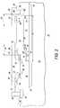
- FIG. 2illustrates an enlarged cross-sectional view of a portion of the Schottky diode of FIG. 1 in accordance with the present invention.
- current carrying electrodemeans an element of a device that carries current through the device such as a source or a drain of an MOS transistor or an emitter or a collector of a bipolar transistor or a cathode or anode of a diode
- a control electrodemeans an element of the device that controls current through the device such as a gate of an MOS transistor or a base of a bipolar transistor.
- doped regions of device structuresare illustrated as having generally straight line edges and precise angular corners. However, those skilled in the art understand that due to the diffusion and activation of dopants, the edges of doped regions generally may not be straight lines and the corners may not be precise angles.
- FIG. 1schematically illustrates an enlarged plan view of a portion of an exemplary form of an integrated circuit 10 that includes a Schottky diode 25 .
- Diode 25is integrated onto a semiconductor substrate 28 with other semiconductor components such as MOS transistors 12 and 17 .
- Transistors 12 and 17are illustrated in simplified form for clarity of the drawings.
- MOS transistor 12includes a source region 13 and a drain region 14 that are formed as doped portions of substrate 28 , and also includes an MOS gate 15 .
- MOS transistor 17includes a source region 18 and a drain region 20 that are formed as doped portions of substrate 28 , and includes an MOS gate 19 .
- transistors 12 and 17 including drain regions 14 and 20are formed as a portion of a region 29 ( FIG. 2 ) of diode 25 .
- Other transistorssuch as MOS transistors 22 and 23 may also be formed on other portions of substrate 28 .
- FIG. 2illustrates an enlarged cross-sectional view of diode 25 along cross-section lines 2 - 2 that are illustrated in FIG. 1 .
- Diode 25is formed to have a high breakdown voltage that generally is greater than approximately five hundred volts (500 V).
- Substrate 28 on which diode 25 is formedgenerally is formed as a lightly doped P-type substrate that has a doping concentration in the range of 1 ⁇ 5 ⁇ 10 14 atoms/cm 3 .
- the light doping of substrate 28facilitates forming other types of semiconductor devices, such as transistors 22 and 23 , on substrate 28 along with diode 25 .
- An N-type doped region 29is formed to extend into substrate 28 from the surface of substrate 28 .
- Diode 25also includes N-type doped regions 30 and 31 generally are formed to overlap respective first and second portions of region 29 . Regions 30 and 31 are formed with a doping concentration that is greater than the doping concentration of region 29 and are spaced apart by a distance 32 . Regions 30 and 31 generally extend trough region 29 into substrate 28 . A portion 33 of region 29 extends between regions 30 and 31 for distance 32 . The combination of the different doping concentration between region 29 to regions 30 and 31 along with distance 32 assists in increasing the breakdown voltage and reducing the forward resistance of diode 25 .
- An anode conductor 49is formed on the surface of substrate 28 and in electrical contact with at least a portion of region 30 in order to form a Schottky junction along the interface of conductor 49 and region 30 .
- Conductor 49functions as the anode of diode 25 while the cathode is formed by regions 30 , 29 , 31 , and through an ohmic contact to a conductor 60 .
- P-type guard ringsare formed as doped regions 36 and 37 extending from the surface into substrate 28 and into region 30 . The guard rings of regions 36 and 37 extend along the outside edges of the Schottky junction and reduce the electric field at the edge of the Schottky junction thereby assisting in increasing the breakdown voltage. As can be seen from the plan view of FIG.
- doped regions 36 and 37generally are one continuous doped region that surrounds the outside edges of the Schottky junction formed at the interface between conductor 49 and region 30 . Typically, regions 36 and 37 overlap the outside interface between conductor 49 and region 30 in order to assist in improving the breakdown voltage of diode 25 .
- the doping concentration of regions 36 and 37usually is greater than the doping concentration of regions 30 and 31 which forms a junction that assists in reducing the electric field at the edge of the Schottky junction.
- a P-type doped region 39is formed within region 31 to also assist in increasing the breakdown voltage of diode 25 .
- the doping concentration of region 39generally is greater than the doping concentration of regions 30 and 31 to also assist in increasing the breakdown voltage.
- the charge of region 39is generally about one-half the charge of region 31 .
- the width of region 39generally has a width that is less than the width of region 31 so that region 39 is spaced a distance 61 from region 59 and also spaced a distance 38 from an opposite edge of region 31 . These spacings also assist in increasing the breakdown voltage.
- Field oxides 40are formed on the surface of substrate 28 . One portion of field oxide 40 is formed to extend from region 59 to an exterior or distal edge of region 31 . A second portion of field oxide 40 extends from region 59 across the surface of substrate 28 overlying regions 31 and 39 past an interior edge of region 31 .
- a third portion of field oxide 40extends from outside the distal edge of regions 29 and 30 to extend to overlie at least a portion of region 30 that is adjacent to the distal edge.
- a thin insulator 41is formed to extend between an edge of region 36 and the edge of oxide 40 that is near region 36 .
- a conductor 46is formed on insulator 41 and a portion of conductor 46 may overlie a portion of oxide 40 .
- Insulator 41 and the portion of conductor 46 overlying insulator 41form an MOS gate.
- Another thin insulator 42that is similar to insulator 41 overlies the portion of region 29 that extends from region 37 to an edge of the portion of oxide 40 that is adjacent to region 31 .
- Another conductor 47is formed on insulator 42 and a portion may overlay onto oxide 40 .
- the portion of conductor 47 overlying insulator 42forms another MOS gate.
- the MOS gatesassist in improving both the breakdown voltage and the forward resistance of diode 25 .
- insulators 41 and 42do not have to overlie the entire distance between oxides 40 and the respective regions 36 or 37 .
- the distance between region 36 and the adjacent oxide 40may be much smaller than the distance between region 37 and the adjacent oxide 40 , thus, insulator 41 and the MOS gate resulting therefrom may be much shorter than insulator 42 and the MOS gate resulting therefrom.
- An insulator materialis applied to the surface of substrate 28 and patterned to form an inner-layer dielectric that includes inner-layer dielectrics 51 , 52 , and 53 .
- Dielectric 51 and a portion of dielectric 52insulate anode conductor 49 from conductors 46 and 47 and another portion of dielectric 52 along with dielectric 53 insulate conductor 60 from other portions of diode 25 .
- a conductor 68is formed on a portion of oxide 40 to form an MOS capacitor overlying at least a portion of distance 61 .
- Conductor 68has a length 69 and is positioned near an adjacent edge of region 59 to assist in improving the breakdown voltage.
- Feed-throughs 55 , 56 , and 57provide an electrical connection between conductor 49 and conductors 46 , 47 , and between conductors 60 and 68 , respectively, in order to provide an electrical potential to the MOS gates and the MOS capacitor.
- a heavily doped region 64is formed on substrate 28 in order to form an ohmic contact to substrate 28 .
- a conductor 65provides a connection to substrate 28 through region 64 .
- the MOS gatesWhen diode 25 is forward biased, the MOS gates receive the voltage from conductor 49 .
- the voltage applied to the MOS gate that includes insulator 42forms an accumulation area within portion 33 of region 29 and near the surface thereof.
- the accumulation areaassists in conducting current from region 30 across the portion of region 29 that is between regions 30 and 31 .
- the current flowcontinues from region 29 through region 31 to region 59 and conductor 60 .
- the low resistance of regions 30 and 31 in addition to the accumulation areaassist in keeping the forward resistance of diode 25 low. Thus, even though a portion of region 29 separates regions 30 and 31 , the accumulation area helps to reduce the forward resistance.
- the drift region of diode 25extends from an edge of region 59 through region 31 through the portion of region 29 that is between regions 30 and 31 , as illustrated by a distance 44 , and through region 30 to the edge of the Schottky junction. Note that an accumulation area is also formed under insulator 41 but it has a minimal effect on current conduction.
- diode 25When diode 25 is reversed biased, several of the features of diode 25 combine to assist in increasing the breakdown voltage of diode 25 .
- the connection to conductor 49ensures that the accumulation areas underlying the MOS gates will not be formed under insulators 41 and 42 , but that the areas will be depleted.
- the MOS gatesassist in increasing the breakdown voltage of diode 25 .
- the reverse voltage applied to diode 25expands the P-N junctions formed between substrate 28 and regions 29 , 30 , 31 thereby forming depletion regions that spread the electric field and assist in increasing the breakdown voltage.
- Spacing the cathode electrode, formed by region 59 and conductor 60 , distance 44 from the anode electrode formed by conductor 49also spreads the electric field over distance 44 and increases the breakdown voltage.
- Spacing region 39 distance 61 from region 59 and distance 35 from the edge of oxide 40minimizes field edge crowding and also increases the breakdown voltage.
- Positioning region 30 distance 34 from the edge of field oxide 40also reduces the intensity of the electric field near the edge of oxide 40 and assists in improving the breakdown voltage.
- Spacing region 30 distance 32 from region 31also reduces the electric field near the edge of oxide 40 and improves the breakdown voltage. Extending conductors 46 and 47 onto the respective portions of oxide 40 assists in reducing the electric field at the edge of oxide 40 .
- regions 36 and 37 to have a higher doping concentration than region 30reduces the injection efficiency by suppressing minority carrier injection.
- the doping concentration of regions 36 and 37is no greater than about one hundred (100) times the doping concentration of region 30 . This provides diode 25 a fast switching time and also reduces both the substrate current and power drain. Adjustment of the doping concentrations of regions 30 and 31 along with spacing 32 minimizes the reverse leakage current and provides diode 25 a more ideal reverse leakage characteristic.
- diode 25is scaled depending on the value of the desired breakdown voltage.
- Distances 38 , 50 , 62 , and length 69are selected based on the desired breakdown voltage.
- diode 25is formed to have a breakdown voltage of no less than about seven hundred volts (700 V).
- distances 32 , 34 , 35 , 44 , 50 , 61 , 62 , and length 69were respectively about nineteen (19) microns, ten (10) microns, twelve (12) microns, seventy (70) microns, eleven (11) microns, 6.5 microns, twenty two (22), and eleven (11) microns.
- regions 36 and 37were about 1 ⁇ 2 ⁇ 10 17 atoms/cm 3 and region 39 had a doping concentration of about 1 ⁇ 2 ⁇ 10 16 atoms/cm 3 .
- conductors 46 and 47 and the associated insulators 41 and 42 , regions 30 , 31 , and 39are optional and may be omitted.
- conductor 49generally is a metal and may be a barrier metal that includes titanium/titanium-nitride layers.
- diode 25is formed to have a breakdown voltage of no less than about eight hundred fifty volts (850 V).
- distances 32 , 34 , 35 , 44 , 50 , 61 , 62 , and length 69were respectively about nineteen (19) microns, ten (10) microns, twelve (12) microns, one hundred (100) microns, eleven (11) microns, 6.5 microns, forty two (42), and thirty one (31) microns.
- the doping of regions 36 and 37was about 1 ⁇ 2 ⁇ 10 17 atoms/cm 3 and region 39 had a doping concentration of about 1 ⁇ 2 ⁇ 10 16 atoms/cm 3 .
- regions 36 and 37may be spaced away from the Schottky junction.
- Region 29may be formed in an epitaxial layer that is formed on a semiconductor substrate.
- the thickness of insulators 41 and 42may be any selected value.
- the words about or approximatelymean that a value of an element has a parameter that is expected to be very close to a stated value or position.
Landscapes
- Electrodes Of Semiconductors (AREA)
- Metal-Oxide And Bipolar Metal-Oxide Semiconductor Integrated Circuits (AREA)
Abstract
Description
Claims (17)
Priority Applications (5)
| Application Number | Priority Date | Filing Date | Title |
|---|---|---|---|
| US11/757,222US8168466B2 (en) | 2007-06-01 | 2007-06-01 | Schottky diode and method therefor |
| TW097115733ATWI430452B (en) | 2007-06-01 | 2008-04-29 | Schottky diode and its method |
| CN2008100971927ACN101315952B (en) | 2007-06-01 | 2008-05-19 | Schottky diode and method therefor |
| KR1020080050032AKR101423065B1 (en) | 2007-06-01 | 2008-05-29 | Schottky diodes and methods for their formation |
| HK09103193.0AHK1125489B (en) | 2007-06-01 | 2009-04-03 | Schottky diode and method therefor |
Applications Claiming Priority (1)
| Application Number | Priority Date | Filing Date | Title |
|---|---|---|---|
| US11/757,222US8168466B2 (en) | 2007-06-01 | 2007-06-01 | Schottky diode and method therefor |
Publications (2)
| Publication Number | Publication Date |
|---|---|
| US20080299751A1 US20080299751A1 (en) | 2008-12-04 |
| US8168466B2true US8168466B2 (en) | 2012-05-01 |
Family
ID=40088778
Family Applications (1)
| Application Number | Title | Priority Date | Filing Date |
|---|---|---|---|
| US11/757,222Active2029-05-03US8168466B2 (en) | 2007-06-01 | 2007-06-01 | Schottky diode and method therefor |
Country Status (4)
| Country | Link |
|---|---|
| US (1) | US8168466B2 (en) |
| KR (1) | KR101423065B1 (en) |
| CN (1) | CN101315952B (en) |
| TW (1) | TWI430452B (en) |
Cited By (4)
| Publication number | Priority date | Publication date | Assignee | Title |
|---|---|---|---|---|
| US20140001517A1 (en)* | 2011-03-08 | 2014-01-02 | K.Eklund Innovation | Semiconductor element |
| US9391195B2 (en) | 2010-12-03 | 2016-07-12 | Taiwan Semiconductor Manufacturing Company, Ltd. | High side gate driver device |
| US9478426B2 (en) | 2014-02-27 | 2016-10-25 | Semiconductor Components Industries, Llc | Semiconductor device and manufacturing method thereof |
| US10593760B2 (en) | 2018-08-02 | 2020-03-17 | Semiconductor Components Industries, Llc | Method for forming trench semiconductor device having Schottky barrier structure |
Families Citing this family (13)
| Publication number | Priority date | Publication date | Assignee | Title |
|---|---|---|---|---|
| US7633135B2 (en)* | 2007-07-22 | 2009-12-15 | Alpha & Omega Semiconductor, Ltd. | Bottom anode Schottky diode structure and method |
| US7476591B2 (en) | 2006-10-13 | 2009-01-13 | Taiwan Semiconductor Manufacturing Company, Ltd. | Lateral power MOSFET with high breakdown voltage and low on-resistance |
| US7989890B2 (en)* | 2006-10-13 | 2011-08-02 | Taiwan Semiconductor Manufacturing Company, Ltd. | Lateral power MOSFET with high breakdown voltage and low on-resistance |
| US7719076B2 (en)* | 2007-08-10 | 2010-05-18 | United Microelectronics Corp. | High-voltage MOS transistor device |
| US20090096039A1 (en)* | 2007-10-10 | 2009-04-16 | United Microelectronics Corp. | High-voltage device and manufacturing method of top layer in high-voltage device |
| US7960786B2 (en)* | 2008-07-09 | 2011-06-14 | Taiwan Semiconductor Manufacturing Company, Ltd. | Breakdown voltages of ultra-high voltage devices by forming tunnels |
| CN102013427B (en)* | 2009-09-07 | 2013-03-06 | 上海宏力半导体制造有限公司 | Avalanche breakdown diode structure and production method thereof |
| US8193602B2 (en)* | 2010-04-20 | 2012-06-05 | Texas Instruments Incorporated | Schottky diode with control gate for optimization of the on state resistance, the reverse leakage, and the reverse breakdown |
| US8629513B2 (en)* | 2011-01-14 | 2014-01-14 | Taiwan Semiconductor Manufacturing Company, Ltd. | HV interconnection solution using floating conductors |
| US8928050B2 (en) | 2013-03-11 | 2015-01-06 | Semiconductor Components Industries, Llc | Electronic device including a schottky contact |
| CN105280634B (en)* | 2014-06-19 | 2018-01-30 | 旺宏电子股份有限公司 | Semiconductor element with metal layer on drift region |
| EA027773B1 (en)* | 2014-12-23 | 2017-08-31 | Открытое акционерное общество "ИНТЕГРАЛ"-управляющая компания холдинга "ИНТЕГРАЛ" | Schottky diode |
| CN106409828B (en)* | 2016-11-30 | 2023-06-02 | 上海芯石微电子有限公司 | A half-bridge rectifier Schottky device suitable for miniaturization packaging and its manufacturing method |
Citations (39)
| Publication number | Priority date | Publication date | Assignee | Title |
|---|---|---|---|---|
| US4035907A (en)* | 1973-08-27 | 1977-07-19 | Signetics Corporation | Integrated circuit having guard ring Schottky barrier diode and method |
| US4220961A (en)* | 1977-12-23 | 1980-09-02 | Siemens Aktiengesellschaft | Monolithic combination of two complementary bipolar transistors |
| US4311532A (en)* | 1979-07-27 | 1982-01-19 | Harris Corporation | Method of making junction isolated bipolar device in unisolated IGFET IC |
| US4333100A (en)* | 1978-05-31 | 1982-06-01 | Harris Corporation | Aluminum Schottky contacts and silicon-aluminum interconnects for integrated circuits |
| US4899199A (en) | 1983-09-30 | 1990-02-06 | International Rectifier Corporation | Schottky diode with titanium or like layer contacting the dielectric layer |
| US5072287A (en)* | 1988-02-08 | 1991-12-10 | Kabushiki Kaisha Toshiba | Semiconductor device and method of manufacturing the same |
| US5109256A (en)* | 1990-08-17 | 1992-04-28 | National Semiconductor Corporation | Schottky barrier diodes and Schottky barrier diode-clamped transistors and method of fabrication |
| US5171699A (en)* | 1990-10-03 | 1992-12-15 | Texas Instruments Incorporated | Vertical DMOS transistor structure built in an N-well CMOS-based BiCMOS process and method of fabrication |
| US5204541A (en)* | 1991-06-28 | 1993-04-20 | Texas Instruments Incorporated | Gated thyristor and process for its simultaneous fabrication with high- and low-voltage semiconductor devices |
| US5418185A (en) | 1993-01-21 | 1995-05-23 | Texas Instruments Incorporated | Method of making schottky diode with guard ring |
| US5475273A (en)* | 1991-12-05 | 1995-12-12 | Sgs Thomson Microelectronics | Smart power integrated circuit with dynamic isolation |
| US5491105A (en)* | 1992-03-25 | 1996-02-13 | Texas Instruments Incorporated | LDMOS transistor with self-aligned source/backgate and photo-aligned gate |
| US5498554A (en)* | 1994-04-08 | 1996-03-12 | Texas Instruments Incorporated | Method of making extended drain resurf lateral DMOS devices |
| US5714921A (en)* | 1994-10-31 | 1998-02-03 | Sony Corporation | Deflection yoke |
| US5751022A (en)* | 1994-03-09 | 1998-05-12 | Kabushiki Kaisha Toshiba | Thyristor |
| US5804849A (en)* | 1996-05-13 | 1998-09-08 | Motorola, Inc. | Compound semiconductor device and method of manufacture |
| US5886383A (en) | 1997-01-10 | 1999-03-23 | International Rectifier Corporation | Integrated schottky diode and mosgated device |
| US6121122A (en)* | 1999-05-17 | 2000-09-19 | International Business Machines Corporation | Method of contacting a silicide-based schottky diode |
| US6303961B1 (en)* | 1998-04-29 | 2001-10-16 | Aqere Systems Guardian Corp. | Complementary semiconductor devices |
| US20030157756A1 (en)* | 2001-07-03 | 2003-08-21 | Intersil Americas Inc. | Mos integrated circuit with reduced on resistance |
| US6613633B2 (en)* | 1999-06-07 | 2003-09-02 | Hynix Semiconductor, Inc. | Method for manufacturing a high power semiconductor device having a field plate extendedly disposed on a gate |
| US6642599B1 (en)* | 1995-08-22 | 2003-11-04 | Mitsubishi Denki Kabushiki Kaisha | Semiconductor device and method of manufacturing the same |
| US6784489B1 (en)* | 1997-03-28 | 2004-08-31 | Stmicroelectronics, Inc. | Method of operating a vertical DMOS transistor with schottky diode body structure |
| US20050145975A1 (en)* | 2001-11-21 | 2005-07-07 | Fuji Electric Co., Ltd. | High power semiconductor device having a schottky barrier diode |
| US6917081B2 (en)* | 2002-04-26 | 2005-07-12 | Ricoh Company, Ltd. | Semiconductor integrated device |
| US20050253216A1 (en)* | 2002-12-17 | 2005-11-17 | Hideaki Tsuchiko | Integrated circuit including a high voltage LDMOS device and low voltage devices |
| US6974753B2 (en)* | 2001-11-21 | 2005-12-13 | Intersil Americas, Inc. | Method of manufacturing lateral MOSFET structure of an integrated circuit having separated device regions |
| US7002187B1 (en) | 2003-06-09 | 2006-02-21 | Micrel, Inc. | Integrated schottky diode using buried power buss structure and method for making same |
| US7056798B2 (en)* | 2000-12-28 | 2006-06-06 | Canon Kabushiki Kaisha | Semiconductor device, method for manufacturing the same, and liquid jet apparatus |
| US7064407B1 (en)* | 2005-02-04 | 2006-06-20 | Micrel, Inc. | JFET controlled schottky barrier diode |
| US20060202254A1 (en)* | 2005-03-10 | 2006-09-14 | Li-Shyue Lai | Multi-level flash memory cell capable of fast programming |
| US20060211227A1 (en)* | 2005-03-21 | 2006-09-21 | Semiconductor Components Industries, Llc | Schottky diode and method of manufacture |
| US20060249759A1 (en)* | 2004-02-17 | 2006-11-09 | Morris Wesley H | Buried guard ring and radiation hardened isolation structures and fabrication methods |
| US20070108534A1 (en)* | 2005-11-15 | 2007-05-17 | International Business Machines Corporation | Schottky barrier diode and method of forming a schottky barrier diode |
| US20070181909A1 (en)* | 2006-02-03 | 2007-08-09 | Semiconductor Components Industries, Llc. | Schottky diode structure with enhanced breakdown voltage and method of manufacture |
| US7282386B2 (en)* | 2005-04-29 | 2007-10-16 | Freescale Semiconductor, Inc. | Schottky device and method of forming |
| US7355260B2 (en)* | 2004-06-30 | 2008-04-08 | Freescale Semiconductor, Inc. | Schottky device and method of forming |
| US20080217725A1 (en)* | 2007-03-08 | 2008-09-11 | Tu Shanghui L | Schottky diode structure with multi-portioned guard ring and method of manufacture |
| US7608907B2 (en)* | 2005-01-06 | 2009-10-27 | Micrel, Inc. | LDMOS gate controlled schottky diode |
Family Cites Families (2)
| Publication number | Priority date | Publication date | Assignee | Title |
|---|---|---|---|---|
| FR2751790B1 (en)* | 1996-07-26 | 1998-11-27 | Sgs Thomson Microelectronics | MONOLITHIC ASSEMBLY OF AN IGBT TRANSISTOR AND A FAST DIODE |
| JPH10335649A (en)* | 1997-05-27 | 1998-12-18 | Mitsubishi Electric Corp | Semiconductor device and manufacturing method thereof |
- 2007
- 2007-06-01USUS11/757,222patent/US8168466B2/enactiveActive
- 2008
- 2008-04-29TWTW097115733Apatent/TWI430452B/enactive
- 2008-05-19CNCN2008100971927Apatent/CN101315952B/ennot_activeExpired - Fee Related
- 2008-05-29KRKR1020080050032Apatent/KR101423065B1/enactiveActive
Patent Citations (41)
| Publication number | Priority date | Publication date | Assignee | Title |
|---|---|---|---|---|
| US4035907A (en)* | 1973-08-27 | 1977-07-19 | Signetics Corporation | Integrated circuit having guard ring Schottky barrier diode and method |
| US4220961A (en)* | 1977-12-23 | 1980-09-02 | Siemens Aktiengesellschaft | Monolithic combination of two complementary bipolar transistors |
| US4333100A (en)* | 1978-05-31 | 1982-06-01 | Harris Corporation | Aluminum Schottky contacts and silicon-aluminum interconnects for integrated circuits |
| US4311532A (en)* | 1979-07-27 | 1982-01-19 | Harris Corporation | Method of making junction isolated bipolar device in unisolated IGFET IC |
| US4899199A (en) | 1983-09-30 | 1990-02-06 | International Rectifier Corporation | Schottky diode with titanium or like layer contacting the dielectric layer |
| US5072287A (en)* | 1988-02-08 | 1991-12-10 | Kabushiki Kaisha Toshiba | Semiconductor device and method of manufacturing the same |
| US5109256A (en)* | 1990-08-17 | 1992-04-28 | National Semiconductor Corporation | Schottky barrier diodes and Schottky barrier diode-clamped transistors and method of fabrication |
| US5171699A (en)* | 1990-10-03 | 1992-12-15 | Texas Instruments Incorporated | Vertical DMOS transistor structure built in an N-well CMOS-based BiCMOS process and method of fabrication |
| US5204541A (en)* | 1991-06-28 | 1993-04-20 | Texas Instruments Incorporated | Gated thyristor and process for its simultaneous fabrication with high- and low-voltage semiconductor devices |
| US5475273A (en)* | 1991-12-05 | 1995-12-12 | Sgs Thomson Microelectronics | Smart power integrated circuit with dynamic isolation |
| US5491105A (en)* | 1992-03-25 | 1996-02-13 | Texas Instruments Incorporated | LDMOS transistor with self-aligned source/backgate and photo-aligned gate |
| US5418185A (en) | 1993-01-21 | 1995-05-23 | Texas Instruments Incorporated | Method of making schottky diode with guard ring |
| US5751022A (en)* | 1994-03-09 | 1998-05-12 | Kabushiki Kaisha Toshiba | Thyristor |
| US5498554A (en)* | 1994-04-08 | 1996-03-12 | Texas Instruments Incorporated | Method of making extended drain resurf lateral DMOS devices |
| US5714921A (en)* | 1994-10-31 | 1998-02-03 | Sony Corporation | Deflection yoke |
| US6642599B1 (en)* | 1995-08-22 | 2003-11-04 | Mitsubishi Denki Kabushiki Kaisha | Semiconductor device and method of manufacturing the same |
| US5804849A (en)* | 1996-05-13 | 1998-09-08 | Motorola, Inc. | Compound semiconductor device and method of manufacture |
| US5886383A (en) | 1997-01-10 | 1999-03-23 | International Rectifier Corporation | Integrated schottky diode and mosgated device |
| US6784489B1 (en)* | 1997-03-28 | 2004-08-31 | Stmicroelectronics, Inc. | Method of operating a vertical DMOS transistor with schottky diode body structure |
| US6303961B1 (en)* | 1998-04-29 | 2001-10-16 | Aqere Systems Guardian Corp. | Complementary semiconductor devices |
| US6121122A (en)* | 1999-05-17 | 2000-09-19 | International Business Machines Corporation | Method of contacting a silicide-based schottky diode |
| US6613633B2 (en)* | 1999-06-07 | 2003-09-02 | Hynix Semiconductor, Inc. | Method for manufacturing a high power semiconductor device having a field plate extendedly disposed on a gate |
| US7056798B2 (en)* | 2000-12-28 | 2006-06-06 | Canon Kabushiki Kaisha | Semiconductor device, method for manufacturing the same, and liquid jet apparatus |
| US20030157756A1 (en)* | 2001-07-03 | 2003-08-21 | Intersil Americas Inc. | Mos integrated circuit with reduced on resistance |
| US20050145975A1 (en)* | 2001-11-21 | 2005-07-07 | Fuji Electric Co., Ltd. | High power semiconductor device having a schottky barrier diode |
| US6974753B2 (en)* | 2001-11-21 | 2005-12-13 | Intersil Americas, Inc. | Method of manufacturing lateral MOSFET structure of an integrated circuit having separated device regions |
| US6917081B2 (en)* | 2002-04-26 | 2005-07-12 | Ricoh Company, Ltd. | Semiconductor integrated device |
| US20050253216A1 (en)* | 2002-12-17 | 2005-11-17 | Hideaki Tsuchiko | Integrated circuit including a high voltage LDMOS device and low voltage devices |
| US7019377B2 (en)* | 2002-12-17 | 2006-03-28 | Micrel, Inc. | Integrated circuit including high voltage devices and low voltage devices |
| US7002187B1 (en) | 2003-06-09 | 2006-02-21 | Micrel, Inc. | Integrated schottky diode using buried power buss structure and method for making same |
| US20060249759A1 (en)* | 2004-02-17 | 2006-11-09 | Morris Wesley H | Buried guard ring and radiation hardened isolation structures and fabrication methods |
| US7355260B2 (en)* | 2004-06-30 | 2008-04-08 | Freescale Semiconductor, Inc. | Schottky device and method of forming |
| US7608907B2 (en)* | 2005-01-06 | 2009-10-27 | Micrel, Inc. | LDMOS gate controlled schottky diode |
| US7064407B1 (en)* | 2005-02-04 | 2006-06-20 | Micrel, Inc. | JFET controlled schottky barrier diode |
| US20060202254A1 (en)* | 2005-03-10 | 2006-09-14 | Li-Shyue Lai | Multi-level flash memory cell capable of fast programming |
| US20060211227A1 (en)* | 2005-03-21 | 2006-09-21 | Semiconductor Components Industries, Llc | Schottky diode and method of manufacture |
| US7282386B2 (en)* | 2005-04-29 | 2007-10-16 | Freescale Semiconductor, Inc. | Schottky device and method of forming |
| US20070108534A1 (en)* | 2005-11-15 | 2007-05-17 | International Business Machines Corporation | Schottky barrier diode and method of forming a schottky barrier diode |
| US20070181909A1 (en)* | 2006-02-03 | 2007-08-09 | Semiconductor Components Industries, Llc. | Schottky diode structure with enhanced breakdown voltage and method of manufacture |
| US7417265B2 (en)* | 2006-02-03 | 2008-08-26 | Semiconductor Components Industries, L.L.C. | Schottky diode structure with enhanced breakdown voltage and method of manufacture |
| US20080217725A1 (en)* | 2007-03-08 | 2008-09-11 | Tu Shanghui L | Schottky diode structure with multi-portioned guard ring and method of manufacture |
Cited By (7)
| Publication number | Priority date | Publication date | Assignee | Title |
|---|---|---|---|---|
| US9391195B2 (en) | 2010-12-03 | 2016-07-12 | Taiwan Semiconductor Manufacturing Company, Ltd. | High side gate driver device |
| US20140001517A1 (en)* | 2011-03-08 | 2014-01-02 | K.Eklund Innovation | Semiconductor element |
| US8969925B2 (en)* | 2011-03-08 | 2015-03-03 | K.Eklund Innovation | Semiconductor element |
| US9478426B2 (en) | 2014-02-27 | 2016-10-25 | Semiconductor Components Industries, Llc | Semiconductor device and manufacturing method thereof |
| US9552993B2 (en) | 2014-02-27 | 2017-01-24 | Semiconductor Components Industries, Llc | Semiconductor device and manufacturing method thereof |
| US10211060B2 (en) | 2014-02-27 | 2019-02-19 | Semiconductor Components Industries, Llc | Semiconductor device and manufacturing method thereof |
| US10593760B2 (en) | 2018-08-02 | 2020-03-17 | Semiconductor Components Industries, Llc | Method for forming trench semiconductor device having Schottky barrier structure |
Also Published As
| Publication number | Publication date |
|---|---|
| KR101423065B1 (en) | 2014-07-25 |
| TWI430452B (en) | 2014-03-11 |
| CN101315952A (en) | 2008-12-03 |
| CN101315952B (en) | 2013-03-20 |
| US20080299751A1 (en) | 2008-12-04 |
| TW200849610A (en) | 2008-12-16 |
| KR20080106050A (en) | 2008-12-04 |
| HK1125489A1 (en) | 2009-08-07 |
Similar Documents
| Publication | Publication Date | Title |
|---|---|---|
| US8168466B2 (en) | Schottky diode and method therefor | |
| US10546950B2 (en) | Semiconductor device | |
| US9577086B2 (en) | Semiconductor device | |
| US7417265B2 (en) | Schottky diode structure with enhanced breakdown voltage and method of manufacture | |
| US10651299B2 (en) | Semiconductor device | |
| US7777278B2 (en) | Lateral semiconductor component with a drift zone having at least one field electrode | |
| US7910410B2 (en) | Integrated low leakage Schottky diode | |
| US7875950B2 (en) | Schottky diode structure with multi-portioned guard ring and method of manufacture | |
| US10593813B2 (en) | Vertical rectifier with added intermediate region | |
| EP2187441A1 (en) | Switching device for electric circuit | |
| US9059329B2 (en) | Power device with integrated Schottky diode and method for making the same | |
| US20220149196A1 (en) | Gate trench power semiconductor devices having improved deep shield connection patterns | |
| US12376319B2 (en) | Support shield structures for trenched semiconductor devices | |
| US10147813B2 (en) | Tunneling field effect transistor | |
| US20130277791A1 (en) | Schottky diode with opposite-polarity schottky diode field guard ring | |
| US20210296477A1 (en) | Semiconductor device | |
| US20120126317A1 (en) | Accufet with integrated clamping circuit | |
| JPH04283968A (en) | Insulating gate type bipolar transistor | |
| EP1022785B1 (en) | Electronic semiconductor power device with integrated diode | |
| CN113161418A (en) | Semiconductor device with a plurality of semiconductor chips | |
| HK1125489B (en) | Schottky diode and method therefor | |
| KR100496105B1 (en) | Driving method and driving circuit of electrostatic induction semiconductor device and electrostatic induction semiconductor device | |
| KR20210003580A (en) | Semiconductor device and method manufacturing the same | |
| CN117012808A (en) | Semiconductor device with a semiconductor device having a plurality of semiconductor chips | |
| HK1023223A (en) | Semiconductor component with linear current-to-voltage characteristics |
Legal Events
| Date | Code | Title | Description |
|---|---|---|---|
| AS | Assignment | Owner name:SEMICONDUCTOR COMPONENTS INDUSTRIES, L.L.C., ARIZO Free format text:ASSIGNMENT OF ASSIGNORS INTEREST;ASSIGNORS:QUDDUS, MOHAMMED TANVIR;TU, SHANGHUI L.;ROZSYPAL, ANTONIN;REEL/FRAME:019371/0282 Effective date:20070601 | |
| AS | Assignment | Owner name:JPMORGAN CHASE BANK, N.A., NEW YORK Free format text:SECURITY AGREEMENT;ASSIGNOR:SEMICONDUCTOR COMPONENTS INDUSTRIES, LLC;REEL/FRAME:019795/0808 Effective date:20070906 Owner name:JPMORGAN CHASE BANK, N.A.,NEW YORK Free format text:SECURITY AGREEMENT;ASSIGNOR:SEMICONDUCTOR COMPONENTS INDUSTRIES, LLC;REEL/FRAME:019795/0808 Effective date:20070906 | |
| AS | Assignment | Owner name:SEMICONDUCTOR COMPONENTS INDUSTRIES, L.L.C., ARIZO Free format text:ASSIGNMENT OF ASSIGNORS INTEREST;ASSIGNOR:HOSSAIN, ZIA;REEL/FRAME:023481/0495 Effective date:20091104 | |
| STCF | Information on status: patent grant | Free format text:PATENTED CASE | |
| AS | Assignment | Owner name:SEMICONDUCTOR COMPONENTS INDUSTRIES, LLC, ARIZONA Free format text:RELEASE OF SECURITY INTEREST;ASSIGNOR:JPMORGAN CHASE BANK, N.A.;REEL/FRAME:033686/0092 Effective date:20100511 | |
| FPAY | Fee payment | Year of fee payment:4 | |
| AS | Assignment | Owner name:DEUTSCHE BANK AG NEW YORK BRANCH, NEW YORK Free format text:SECURITY INTEREST;ASSIGNOR:SEMICONDUCTOR COMPONENTS INDUSTRIES, LLC;REEL/FRAME:038620/0087 Effective date:20160415 | |
| AS | Assignment | Owner name:DEUTSCHE BANK AG NEW YORK BRANCH, AS COLLATERAL AG Free format text:CORRECTIVE ASSIGNMENT TO CORRECT THE INCORRECT PATENT NUMBER 5859768 AND TO RECITE COLLATERAL AGENT ROLE OF RECEIVING PARTY IN THE SECURITY INTEREST PREVIOUSLY RECORDED ON REEL 038620 FRAME 0087. ASSIGNOR(S) HEREBY CONFIRMS THE SECURITY INTEREST;ASSIGNOR:SEMICONDUCTOR COMPONENTS INDUSTRIES, LLC;REEL/FRAME:039853/0001 Effective date:20160415 Owner name:DEUTSCHE BANK AG NEW YORK BRANCH, AS COLLATERAL AGENT, NEW YORK Free format text:CORRECTIVE ASSIGNMENT TO CORRECT THE INCORRECT PATENT NUMBER 5859768 AND TO RECITE COLLATERAL AGENT ROLE OF RECEIVING PARTY IN THE SECURITY INTEREST PREVIOUSLY RECORDED ON REEL 038620 FRAME 0087. ASSIGNOR(S) HEREBY CONFIRMS THE SECURITY INTEREST;ASSIGNOR:SEMICONDUCTOR COMPONENTS INDUSTRIES, LLC;REEL/FRAME:039853/0001 Effective date:20160415 | |
| MAFP | Maintenance fee payment | Free format text:PAYMENT OF MAINTENANCE FEE, 8TH YEAR, LARGE ENTITY (ORIGINAL EVENT CODE: M1552); ENTITY STATUS OF PATENT OWNER: LARGE ENTITY Year of fee payment:8 | |
| AS | Assignment | Owner name:FAIRCHILD SEMICONDUCTOR CORPORATION, ARIZONA Free format text:RELEASE OF SECURITY INTEREST IN PATENTS RECORDED AT REEL 038620, FRAME 0087;ASSIGNOR:DEUTSCHE BANK AG NEW YORK BRANCH, AS COLLATERAL AGENT;REEL/FRAME:064070/0001 Effective date:20230622 Owner name:SEMICONDUCTOR COMPONENTS INDUSTRIES, LLC, ARIZONA Free format text:RELEASE OF SECURITY INTEREST IN PATENTS RECORDED AT REEL 038620, FRAME 0087;ASSIGNOR:DEUTSCHE BANK AG NEW YORK BRANCH, AS COLLATERAL AGENT;REEL/FRAME:064070/0001 Effective date:20230622 | |
| MAFP | Maintenance fee payment | Free format text:PAYMENT OF MAINTENANCE FEE, 12TH YEAR, LARGE ENTITY (ORIGINAL EVENT CODE: M1553); ENTITY STATUS OF PATENT OWNER: LARGE ENTITY Year of fee payment:12 |