US8168456B2 - Vertical cavity surface emitting laser with undoped top mirror - Google Patents
Vertical cavity surface emitting laser with undoped top mirrorDownload PDFInfo
- Publication number
- US8168456B2 US8168456B2US12/979,248US97924810AUS8168456B2US 8168456 B2US8168456 B2US 8168456B2US 97924810 AUS97924810 AUS 97924810AUS 8168456 B2US8168456 B2US 8168456B2
- Authority
- US
- United States
- Prior art keywords
- forming
- mirror
- layer
- doped
- top mirror
- Prior art date
- Legal status (The legal status is an assumption and is not a legal conclusion. Google has not performed a legal analysis and makes no representation as to the accuracy of the status listed.)
- Expired - Lifetime
Links
Images


Classifications
- H—ELECTRICITY
- H01—ELECTRIC ELEMENTS
- H01S—DEVICES USING THE PROCESS OF LIGHT AMPLIFICATION BY STIMULATED EMISSION OF RADIATION [LASER] TO AMPLIFY OR GENERATE LIGHT; DEVICES USING STIMULATED EMISSION OF ELECTROMAGNETIC RADIATION IN WAVE RANGES OTHER THAN OPTICAL
- H01S5/00—Semiconductor lasers
- H01S5/10—Construction or shape of the optical resonator, e.g. extended or external cavity, coupled cavities, bent-guide, varying width, thickness or composition of the active region
- H01S5/18—Surface-emitting [SE] lasers, e.g. having both horizontal and vertical cavities
- H01S5/183—Surface-emitting [SE] lasers, e.g. having both horizontal and vertical cavities having only vertical cavities, e.g. vertical cavity surface-emitting lasers [VCSEL]
- H01S5/18308—Surface-emitting [SE] lasers, e.g. having both horizontal and vertical cavities having only vertical cavities, e.g. vertical cavity surface-emitting lasers [VCSEL] having a special structure for lateral current or light confinement
- H01S5/18311—Surface-emitting [SE] lasers, e.g. having both horizontal and vertical cavities having only vertical cavities, e.g. vertical cavity surface-emitting lasers [VCSEL] having a special structure for lateral current or light confinement using selective oxidation
- H01S5/18313—Surface-emitting [SE] lasers, e.g. having both horizontal and vertical cavities having only vertical cavities, e.g. vertical cavity surface-emitting lasers [VCSEL] having a special structure for lateral current or light confinement using selective oxidation by oxidizing at least one of the DBR layers
- H—ELECTRICITY
- H01—ELECTRIC ELEMENTS
- H01S—DEVICES USING THE PROCESS OF LIGHT AMPLIFICATION BY STIMULATED EMISSION OF RADIATION [LASER] TO AMPLIFY OR GENERATE LIGHT; DEVICES USING STIMULATED EMISSION OF ELECTROMAGNETIC RADIATION IN WAVE RANGES OTHER THAN OPTICAL
- H01S5/00—Semiconductor lasers
- H01S5/10—Construction or shape of the optical resonator, e.g. extended or external cavity, coupled cavities, bent-guide, varying width, thickness or composition of the active region
- H01S5/18—Surface-emitting [SE] lasers, e.g. having both horizontal and vertical cavities
- H01S5/183—Surface-emitting [SE] lasers, e.g. having both horizontal and vertical cavities having only vertical cavities, e.g. vertical cavity surface-emitting lasers [VCSEL]
- H01S5/18308—Surface-emitting [SE] lasers, e.g. having both horizontal and vertical cavities having only vertical cavities, e.g. vertical cavity surface-emitting lasers [VCSEL] having a special structure for lateral current or light confinement
- H01S5/18322—Position of the structure
- H01S5/1833—Position of the structure with more than one structure
- H—ELECTRICITY
- H01—ELECTRIC ELEMENTS
- H01S—DEVICES USING THE PROCESS OF LIGHT AMPLIFICATION BY STIMULATED EMISSION OF RADIATION [LASER] TO AMPLIFY OR GENERATE LIGHT; DEVICES USING STIMULATED EMISSION OF ELECTROMAGNETIC RADIATION IN WAVE RANGES OTHER THAN OPTICAL
- H01S5/00—Semiconductor lasers
- H01S5/10—Construction or shape of the optical resonator, e.g. extended or external cavity, coupled cavities, bent-guide, varying width, thickness or composition of the active region
- H01S5/18—Surface-emitting [SE] lasers, e.g. having both horizontal and vertical cavities
- H01S5/183—Surface-emitting [SE] lasers, e.g. having both horizontal and vertical cavities having only vertical cavities, e.g. vertical cavity surface-emitting lasers [VCSEL]
- H01S5/18341—Intra-cavity contacts
- H—ELECTRICITY
- H01—ELECTRIC ELEMENTS
- H01S—DEVICES USING THE PROCESS OF LIGHT AMPLIFICATION BY STIMULATED EMISSION OF RADIATION [LASER] TO AMPLIFY OR GENERATE LIGHT; DEVICES USING STIMULATED EMISSION OF ELECTROMAGNETIC RADIATION IN WAVE RANGES OTHER THAN OPTICAL
- H01S5/00—Semiconductor lasers
- H01S5/10—Construction or shape of the optical resonator, e.g. extended or external cavity, coupled cavities, bent-guide, varying width, thickness or composition of the active region
- H01S5/18—Surface-emitting [SE] lasers, e.g. having both horizontal and vertical cavities
- H01S5/183—Surface-emitting [SE] lasers, e.g. having both horizontal and vertical cavities having only vertical cavities, e.g. vertical cavity surface-emitting lasers [VCSEL]
- H01S5/18361—Structure of the reflectors, e.g. hybrid mirrors
- H01S5/18369—Structure of the reflectors, e.g. hybrid mirrors based on dielectric materials
- H—ELECTRICITY
- H01—ELECTRIC ELEMENTS
- H01S—DEVICES USING THE PROCESS OF LIGHT AMPLIFICATION BY STIMULATED EMISSION OF RADIATION [LASER] TO AMPLIFY OR GENERATE LIGHT; DEVICES USING STIMULATED EMISSION OF ELECTROMAGNETIC RADIATION IN WAVE RANGES OTHER THAN OPTICAL
- H01S5/00—Semiconductor lasers
- H01S5/20—Structure or shape of the semiconductor body to guide the optical wave ; Confining structures perpendicular to the optical axis, e.g. index or gain guiding, stripe geometry, broad area lasers, gain tailoring, transverse or lateral reflectors, special cladding structures, MQW barrier reflection layers
- H01S5/2054—Methods of obtaining the confinement
- H01S5/2081—Methods of obtaining the confinement using special etching techniques
- H01S5/2086—Methods of obtaining the confinement using special etching techniques lateral etch control, e.g. mask induced
- H—ELECTRICITY
- H01—ELECTRIC ELEMENTS
- H01S—DEVICES USING THE PROCESS OF LIGHT AMPLIFICATION BY STIMULATED EMISSION OF RADIATION [LASER] TO AMPLIFY OR GENERATE LIGHT; DEVICES USING STIMULATED EMISSION OF ELECTROMAGNETIC RADIATION IN WAVE RANGES OTHER THAN OPTICAL
- H01S5/00—Semiconductor lasers
- H01S5/30—Structure or shape of the active region; Materials used for the active region
- H01S5/305—Structure or shape of the active region; Materials used for the active region characterised by the doping materials used in the laser structure
- H01S5/3095—Tunnel junction
- H—ELECTRICITY
- H01—ELECTRIC ELEMENTS
- H01S—DEVICES USING THE PROCESS OF LIGHT AMPLIFICATION BY STIMULATED EMISSION OF RADIATION [LASER] TO AMPLIFY OR GENERATE LIGHT; DEVICES USING STIMULATED EMISSION OF ELECTROMAGNETIC RADIATION IN WAVE RANGES OTHER THAN OPTICAL
- H01S5/00—Semiconductor lasers
- H01S5/30—Structure or shape of the active region; Materials used for the active region
- H01S5/32—Structure or shape of the active region; Materials used for the active region comprising PN junctions, e.g. hetero- or double- heterostructures
- H01S5/3211—Structure or shape of the active region; Materials used for the active region comprising PN junctions, e.g. hetero- or double- heterostructures characterised by special cladding layers, e.g. details on band-discontinuities
Definitions
- the inventiongenerally relates to lasers. More specifically, the invention relates to Vertical Cavity Surface Emitting Lasers (VCSELs).
- VCSELsVertical Cavity Surface Emitting Lasers
- Lasersare commonly used in many modern components. One use that has recently become more common is the use of lasers in data networks. Lasers are used in many fiber optic communication systems to transmit digital data on a network.
- a lasermay be modulated by digital data to produce an optical signal, including periods of light and dark output that represents a binary data stream.
- the lasersoutput a high optical output representing binary highs and a lower power optical output representing binary lows.
- the laseris constantly on, but varies from a high optical output to a lower optical output.
- Optical networkshave various advantages over other types of networks such as copper wire based networks. For example, many existing copper wire networks operate at near maximum possible data transmission rates and at near maximum possible distances for copper wire technology. On the other hand, many existing optical networks exceed, both in data transmission rate and distance, the maximums that are possible for copper wire networks. That is, optical networks are able to reliably transmit data at higher rates over further distances than is possible with copper wire networks.
- a VCSELVertical Cavity Surface Emitting Laser
- GaAsGallium Arsenide
- the VCSELincludes a bottom mirror constructed on the semiconductor wafer.
- the bottom mirrorincludes a number of alternating high and low index of refraction layers. As light passes from a layer of one index of refraction to another, a portion of the light is reflected. By using a sufficient number of alternating layers, a high percentage of light can be reflected by the mirror.
- An active region that includes a number of quantum wellsis formed on the bottom mirror.
- the active regionforms a PN junction sandwiched between the bottom mirror and a top mirror, which are of opposite conductivity type (i.e. a p-type mirror and an n-type mirror).
- Free carriers in the form of holes and electronsare injected into the quantum wells when the PN junction is forward biased by an electrical current.
- the injected minority carriersform a population inversion (i.e. a higher concentration of free carriers in the conduction band than electrons in the valance band) in the quantum wells that produces optical gain.
- Optical gainoccurs when photons in the active region cause electrons to move from the conduction band to the valance band which produces additional photons.
- the active regionmay also include an oxide aperture formed using one or more oxide layers formed in the top and/or bottom mirrors near the active layer.
- the oxide apertureserves both to form an optical cavity and to direct the bias current through the central region of the cavity that is formed.
- a top mirroris formed on the active region.
- the top mirroris similar to the bottom mirror in that it generally comprises a number of layers that alternate between a high index of refraction and a lower index of refraction.
- the top mirrorhas fewer mirror periods of alternating high index and low index of refraction layers, to enhance light emission from the top of the VCSEL.
- the laserfunctions when a current is passed through the PN junction to inject free carriers into the active region. Recombination of the injected free carriers from the conduction band quantum wells to the valence band quantum wells results in photons that begin to travel in the laser cavity defined by the mirrors. The mirrors reflect the photons back and forth.
- the bias currentis sufficient to produce a population inversion between the quantum well states at the wavelength supported by the cavity optical gain is produced in the quantum wells.
- the optical gainis equal to the cavity loss laser oscillation occurs and the laser is said to be at threshold bias and the VCSEL begins to ‘lase’ as the optically coherent photons are emitted from the top of the VCSEL.
- the VCSELis generally formed as a semiconductor diode.
- a diodeis formed from a pn junction that includes a p-type material and an n-type material.
- p-type materialsare semiconductor materials, such as Gallium Arsenide (GaAs) doped with a material such as carbon that causes free holes, or positive charge carriers to be formed in the semiconductor material.
- N-type materialsare semiconductor materials such as GaAs doped with a material such as silicon to cause free electrons, or negative charge carriers, to be formed in the semiconductor material.
- the top mirroris doped with p-type dopants where the bottom mirror is doped with n-type dopants to allow for current flow to inject minority carrier electrons and holes into the active region.
- Doping the top mirrorresults in various difficulties in lasers designed to produce longer wavelengths. For example, as wavelength of the emitted light increases, free carrier absorption also increases in the doped p-type top mirror. This added mirror loss requires higher optical gain in the quantum wells to achieve threshold bias. To achieve higher gain a higher current (i.e. threshold current) must be passed through the VCSEL to cause the VCSEL to lase. The higher mirror loss also lowers the efficiency of the VCSEL. This increases the internal heating and limits the amount of power that a VCSEL can output.
- threshold currenti.e. threshold current
- the restriction on doping level caused by absorption in the top mirrordecreases the electrical conductivity of the VCSEL which causes resistive heating in the VCSEL which limits power output, and degrades reliability.
- ramps of material composition at the boundaries between layers in the mirrorsdegrade thermal impedance and reflectivity. If the VCSEL is not able to conduct heat away from the active region, the operating temperature of the VCSEL may rise. If the mirror layers have a degraded reflectivity, additional layers may need to be used resulting in increased impedance and further increased heating of the VCSEL. Excessive heating can damage the VCSEL or shorten the useful life of the VCSEL or degrade its performance.
- the VCSELincludes an epitaxial structure.
- the epitaxial structureis deposited on a substrate.
- a bottom mirroris formed on the substrate and is doped so as to be conductive with the same conductivity type as the substrate.
- An active layer that contains quantum wellsis disposed on the bottom mirror.
- One or more periodically doped conduction layers with conductivity type opposite that of the substrate and bottom mirrorare formed on the quantum wells.
- the periodically doped conduction layersare most heavily doped at locations where the optical electric field will be near or at a minimum when the VCSEL is lasing.
- An essentially undoped top mirroris formed on the heavily doped conduction layer.
- Portions of the undoped top mirrorare selectively removed to form an essentially circular mesa of the undoped top mirror over the center of the VCSEL active area and to expose the surface of the periodically doped conduction layer.
- Ohmic contactis made to the top surface of the conduction layer outside the diameter of the undoped top mirror mesa.
- a current aperturesuch as an oxide, or patterned pn junction, or patterned tunnel junction is disposed between the majority of the top mirror and the active region.
- Another embodimentincludes a method of fabricating a VCSEL.
- the methodincludes forming a bottom mirror on a substrate.
- Forming a bottom mirrorincludes forming alternating layers of high and low index of refraction materials. At least a portion of the materials in the bottom mirror are doped and have the same conductivity type as the substrate.
- the methodalso includes forming an active layer that contains quantum wells on the bottom mirror.
- the methodfurther includes forming a heavily doped conduction layer on the active layer that has the opposite conductivity type than the bottom mirror and substrate.
- Forming the conduction layerincludes forming the conduction layer such that doping is introduced into the conduction layer at locations where the optical electric field would be at or near a minimum when the VCSEL is lasing.
- the methodalso includes forming a top mirror on the conduction layer.
- Forming the top mirrorincludes forming an essentially undoped top mirror which may not have grades at the interfaces of the mirror. Portions of the undoped top mirror are selectively removed to form an essentially circular mesa of the undoped top mirror over the center of the VCSEL active area and to expose the surface of the periodically doped conduction layer. Ohmic contact is made to the top surface of the conduction layer outside the diameter of the undoped top mirror mesa.
- Another embodimentincludes a VCSEL formed on a substrate including an undoped top mirror which may not have grades at the interfaces.
- a periodically doped conduction layeris interposed between the undoped top mirror and the active region.
- a doped bottom mirroris connected to the active region.
- An intracavity contactis connected to the top surface of the periodically doped conduction layer.
- a bottom contactis connected to the substrate.
- a current apertureis disposed between the periodically doped conduction layer and the active region.
- some embodiments of the inventionuse an undoped top mirror to reduce absorption of free carriers in the top mirror. This allows for better performance of certain long wavelength VCSELs, such as the 1310 nm VCSEL. Additionally, embodiments using periodic doping reduce free carrier absorption in other parts of the VCSEL to improve VCSEL performance.
- the improved thermal conductivity caused by the lack of grades at the interfaces of the undoped top mirroris used advantageously to remove heat from the VCSEL by extending the top contact metal layer up the sides of the undoped top mirror mesa with partial coverage of the top surface of the top mirror mesa. When gold is used as the top contact metal the high thermal conductivity of the gold layer contacting the undoped portions of the top mirror serves to conduct heat away from the active area of the VCSEL to improve VCSEL performance.
- Another embodimentincludes a VCSEL with a tunnel junction at the interface between the conduction layer and the undoped top mirror.
- the tunnel junctioncomprises a thin heavily doped n-type layer of GaAs and a thin heavily doped p-type layer of GaAs. These two layers are sufficiently heavily doped that the resulting diode conducts by tunneling at zero bias.
- the desired low lateral sheet resistanceis provided by the heavily doped n-type layer which has much higher carrier mobility than the heavily doped p-type layer.
- the intracavity contactis made to the heavily doped n-type layer using an alloyed Au:Ge contact layer under the top metal layer that forms the intracavity bond pad.
- the heavily doped n- and p-type layersare located at a minimum of the optical E-field to minimize free carrier absorption.
- FIG. 1illustrates a VCSEL with an undoped top mirror an intracavity contact
- FIG. 2illustrates a graph of electric field in a VCSEL versus the layers in an epitaxial structure
- FIG. 3Aillustrates a first photolithographic mask which defines an initial oxide removal pattern. This mask layer is also used to create fiducial marks used in the alignment of subsequent masks.
- FIG. 3Billustrates photolithographic mask including a reactive ion etch mask
- FIG. 3Cillustrates photolithographic masks including a trench photomask
- FIG. 3Dillustrates photolithographic masks including a proton bombardment isolation mask
- FIG. 3Eillustrates photolithographic masks including a slope pattern mask for reactive ion etching (RIE);
- FIG. 3Fillustrates photolithographic mask including a dielectric etch mask
- FIG. 3Gillustrates a photolithographic mask including a metal contact pattern.
- One embodimentimproves performance of VCSELs at higher wavelengths by reducing or eliminating doping in the top mirror to minimize free carrier absorption.
- An intracavity contactcan be connected to the active region via conduction layers to provide current to the active region for producing photons.
- Other layers of the VCSEL structurealso use a method of periodic doping where dopants are more heavily concentrated at locations where the electrical field will be at a minimum so as to reduce free carrier absorption.
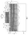
- an illustrative embodimentincludes a VCSEL 100 with an undoped top mirror 102 and intracavity contact 104 .
- the VCSELis formed from an epitaxial structure 105 that includes various layers of semiconductor materials that will be described in more detail below.
- the eptiaxial structure 105goes through various etching, deposition and oxide growth stages in the VCSEL 100 formation.
- the VCSEL 100is formed on a substrate 106 .
- the substrate 106in this example, is a gallium arsenide (GaAs) substrate. In other embodiments, the substrate 106 may be other material such as other III IV semiconductor materials.
- a bottom mirror 108is formed on the substrate 106 .
- the bottom mirrorhas the same conductivity type as the substrate.
- the bottom mirror and substrateare n-type.
- the bottom mirror 108is a distributed Bragg reflector (DBR) mirror that includes a number of alternating layers of high and low index of refraction materials.
- the bottom mirror 108includes alternating layers of aluminum arsenide (AlAs) and GaAs.
- the bottom mirror 108is typically doped with a donor impurity such as silicon such that the bottom mirror is conductive.
- a special rampmay be formed between the alternating layers of the bottom mirror 108 .
- the rampprovides a gradual change of electronic affinity between the alternating layers.
- the rampincludes a step from AlAs to Al x Ga 1-x As where x is about 33 to 35% followed by an essentially linear ramp of aluminum composition from about 33% to zero (GaAs) after the step.
- the electron affinityis essentially constant across the step, and thus there is no need to ramp through the step. Examples of similar special ramps are disclosed in U.S. patent application Ser. No. 10/767,920, titled “Electron Affinity Engineered VCSELs” filed Jan. 29, 2004.
- An active region 110is formed on the bottom mirror 108 and is bounded laterally by proton bombarded isolation implants 111 which will be discussed in more detail below and isolation trenches 113 .
- the active region 110includes quantum wells 112 .
- the central region of the quantum wells 112 under the oxide aperture 124may also be referred to as the optical gain region.
- This central region of the quantum wells 112is the location where current through the active region 110 and the presence of injected free carriers causes population inversion and optical gain. These free carriers moving from conduction band quantum well states to valence band quantum well states (i.e. across the band gap) cause the emission of photons.
- An oxide layer 114is formed in the conduction layer region 123 above the active layer 110 to provide an aperture 124 for lateral definition of the laser optical cavity and for directing bias current to the central region of the VCSEL active region 110 .
- the conduction layer region 123has a conductivity type opposite that of the substrate and bottom mirror and further includes a periodically doped top portion 116 .
- the conduction layer region 123is p-type.
- Two or three periodically doped layers 116are heavily doped at the optical electric field minima so as to provide a low resistance lateral current path for directing current from the Ohmic contact region 125 to the central region of the active region 110 located under the oxide aperture 124 .
- the conduction layers 116may be doped at between about 5 ⁇ 10 19 to 1 ⁇ 10 20 at some distance less than about 1 ⁇ 10 ⁇ 18 away from the minimum of the optical electric field.
- conduction layers 116there are two periodically doped conduction layers 116 each having a sheet resistance of about 500 Ohms per square are doped with an acceptor impurity such as carbon. Using two conduction layers results in a total sheet resistance of about 250 Ohms per square.
- Another embodiment of the inventionuses three periodically doped conduction layers 116 in the top portion of the conduction layer region 123 .
- Each of the periodically doped conduction layers 116has a sheet resistance of about 500 Ohms per square.
- Using three conduction layersresults in a total sheet resistance of about 167 Ohms. This provides a significant reduction in series resistance which lowers power dissipation and improves VCSEL performance.
- a dielectric layer 118is formed on the conduction layers 116 .
- the dielectric 118is taper etched to facilitate step coverage of the top contact metal 104 that extends from the Ohmic contact region 125 to the top metal bond pad (not shown in FIG. 1 ).
- Thick dielectric 118is provided under the bond pad to decrease the capacitance between the bond pad metal and the surface of the proton bombarded region under the bond pad which comprises the conduction layer region 123 , the active layer 110 , and a major portion 111 of the n-type mirror 108 .
- the intracavity contact metal 104is connected to the top conduction layer 116 forming a top Ohmic contact.
- the intracavity contactsare also formed such that the intracavity contacts 104 are also connected to a bond pad (not shown) for connecting the VCSEL 100 to a current source.
- the intracavity contacts 104extend up around the sides of the undoped top mirror 102 . This provides a thermal path for dissipating thermal energy generated in the active region 110 and the conduction layer region 123 .
- the undoped top mirror 102 in this exampleis part of a mesa structure.
- the undoped top mirror 102may be for example alternating layers of higher and lower index of refraction materials.
- the top mirrormay include alternating layers of GaAs and Aluminum Gallium Arsenide (AlGaAs).
- AlGaAsAluminum Gallium Arsenide
- One present embodimentincludes AlGaAs layers that are 87.5% aluminum.
- Other embodimentsmay include AlGaAs layers that are generally in the range of 70-100% aluminum.
- the VCSEL 100may be constructed using a process that uses an oxide to seal the top mirror 102 during the fabrication process of the VCSEL 100 .
- the top mirror 102is sealed from the high temperature wet oxidation process used to form the oxide layer 114 , an alternate construction including alternating layers of GaAs and AlAs may be used for the top mirror 102 .
- Layers of GaAs and AlAsmay be advantageous in implementing embodiments with better thermal characteristics. Better thermal characteristics result because binary materials such as GaAs and AlAs are more thermally conductive than alloy materials such as AlGaAs.
- the use of binary materials in the top mirroralso provides the greatest refractive index difference between the mirror layers which makes it possible to achieve the desired top mirror reflectivity with a minimum number of layer pairs.
- the VCSEL 100further includes an oxide dielectric 120 to protect portions of the VCSEL 100 .
- the oxide dielectric 120has an optical thickness of ⁇ /2 of the VCSEL wavelength to provide maximum optical reflectivity at the top exit surface of the VCSEL 100 .
- one of the conduction layers 116may be replaced with a tunnel junction.
- a tunnel junctiongenerally comprises a highly conductive diode.
- the highly conductive diodeincludes a thin heavily doped p layer of GaAs and a thin heavily doped layer of n-type GaAs.
- the tunnel junction layersare sufficiently heavily doped such that the resulting diode conducts by tunneling at zero bias.
- Low lateral sheet resistanceis provided by the heavily doped n-type layer, which has much higher carrier mobility than the heavily doped p-type layer.
- the intracavity contact 104is coupled to the heavily doped n-type layer using an alloyed Au:Ge contact layer under the top metal layer that forms the intracavity bond pad.
- the heavily doped n and p-type layersare located at or near minimums of the optical electronic field to minimize free carrier absorption. While a tunnel junction alone may not have sufficient electrical conductivity to carry the appropriate currents needed to the active region 110 , using a large tunnel junction with a large surface area in combination with a conduction layer 116 may provide an adequate amount of conduction. This may allow for the use of a less than optimal tunnel junction in the VCSEL 100 .
- Very highly conductive tunnel junctionsmay be difficult to form in VCSEL structures. This difficulty results in part due to the high temperatures used when forming additional layers of the epitaxial structure 105 subsequent to formation of tunnel junctions. These high temperatures cause a diffusion of the high concentration dopants used in the heavily doped layers in the tunnel junction. This diffusion degrades the tunnel junction characteristics. However, using a less than optimal tunnel junction in conjunction with a conduction layer 116 may provide a suitable current path for directing current to the active region 110 . Additionally, a highly doped optimal tunnel junction may be used if the upper mirror is deposited at a low temperature made possible by the lack of doping and conduction. The upper mirror may be, simply a dielectric stack.
- an undoped bottom mirrorwhich may be grown on semi-insulating substrates, can be used as the bottom mirror 108 .
- Thisfurther reduces free carrier absorption, and further allows for improved reflectivity and thermal conductivity by eliminating ramps between the bottom mirror 108 layers.
- a periodically doped n lower spacer(not shown) is grown between the bottom mirror 108 and the quantum wells 112 .
- a second intracavity contactis made after etching to the periodically doped lower spacer.
- Etching to the periodically doped lower spacerincludes using an etch which stops on or in the periodically doped lower spacer.
- Another embodiment of the inventionimplements a periodically doped conduction layer below the active region (as opposed to above the active region as shown in FIG. 1 ) and an undoped bottom mirror between the bottom conduction layer and the substrate.
- Cathode and anode Ohmic contactsmay be provided to the VCSEL active layer by using two intracavity contacts.
- Using an undoped bottom mirrorlowers the absorption loss in the bottom mirror and improves VCSEL performance by lowering threshold current and increasing efficiency.
- FIG. 2a graph that shows the optical electric field versus the layers in the epitaxial structure 105 ( FIG. 1 ).
- FIG. 2illustrates other layers that may be included in the epitaxial structure 105 ( FIG. 1 ). Further, FIG. 2 is used to illustrate where dopants may be heavily concentrated or avoided to reduce free carrier absorption in the epitaxial structure 105 ( FIG. 1 ).
- the electric field illustrated in FIG. 2is shown as an absolute (positive) value, whereas in reality, the electric field may be positive or negative in various locations of the epitaxial structure 105 ( FIG. 1 ). However, because free carrier absorption is a function of the electric field squared, which is always positive, the absolute value of the electric field is useful for designing the epitaxial structure 105 ( FIG. 1 ).
- FIG. 2illustrates the top mirror 102 .
- the top mirror 102is undoped so as to reduce free carrier absorption. Free carrier absorption is a function of the level of doping. Thus by not including any dopants in the top mirror 102 , free carrier absorption in the top mirror 102 is avoided.
- the etch stop layer 122is used in fabricating the VCSL 100 ( FIG. 1 ). This will be explained in more detail in conjunction with the description of FIGS. 3A through 3G below.
- the etch stop layer 122can be used to ensure that etching done to expose the surface of the conduction layer 116 and that the etching does not remove a thin heavy doped layer on the surface of the conduction layer 116 . This insures that the intracavity contacts 104 may be properly attached to the conduction layers 116 to form low resistance Ohmic contacts.
- the etch stop layer 122may be undoped.
- the etch stop layer 122 in this exampleis a grown AlGaAs layer with aluminum composition between 60% and 87.5%. Periodic doping involves heavily doping a layer at locations where the electric field will be at a minimum when the VCSEL 100 ( FIG. 1 ) is in operation. This helps to reduce free carrier absorption in a layer.
- the periodically doped conduction layer 116is GaAs.
- a stop etchis used to expose the surface of the conduction layer 116 that etches AlGaAs but does not etch GaAs.
- the etch rate of the stop etchis a function of the aluminum composition which can be optimized to result in the optimum process control. Periodic doping methods are discussed in U.S. Pat. No. 6,064,683 titled Bandgap Isolated Light Emitter issued to Ralph Johnson, which is incorporated herein by reference.
- the conduction layers 116also use periodic doping to heavily dope portions of the conduction layers 116 where the electric field is at a minimum while controlling doping to a lower impurity concentration when the electric field is not zero.
- a periodically doped lower spacer 223separates the active layer 110 from the bottom mirror 108 .
- the AlGaAs layer 224 with, in one embodiment, 96% aluminumforms the oxide layer 114 during high temperature wet oxidation. This high aluminum AlGaAs layer 224 is formed by digital alloy growth.
- the digital alloy growthincludes 16 layer pairs of 0.87 nm 87.5% AlGaAs and 1.76 nm of AlAs to give a total layer thickness of 43.68 nm with an average composition of 96% Al and 4% Ga in the AlGaAs.
- the first 8 layer pairsstart with AlGaAs and end with AlAs.
- the last 8 layer pairsstart with AlAs and end with AlGaAs.
- the rate of oxidation of AlGaAsis a rapidly increasing function of Al composition.
- the central AlAs layerprovides a sharp point on the oxidation front which is beneficial in limiting optical scattering loss at the oxide aperture and improves VCSEL performance.
- FIGS. 3A through 3Gvarious masks used in lithography steps for manufacturing the VCSEL 100 ( FIG. 1 ) on a GaAs wafer are shown.
- the lithographic stepsare performed on an epitaxial structure so as to form an epitaxial structure such as the epitaxial structure 105 shown in FIG. 1 .
- a plasma oxideis deposited on the epitaxial structure.
- the plasma oxide depositionis approximately 2190 Angstroms of SiO 2 . 2190 Angstroms is ⁇ /4 wavelength in a 1310 nm laser.
- FIG. 3Ashows the area in each VCSEL device where the initial ⁇ /4 oxide is removed.
- This first mask layer 350is also used to form fiducial marks for subsequent mask alignments.
- This maskalso provides a feature that leaves ⁇ /4 oxide 352 over the aperture 124 of the VCSEL 100 ( FIG. 1 ).
- FIG. 3Billustrates a deep RIE (reactive ion etch) photo resist etch mask 354 superimposed on the first mask 350 .
- the RIE etch mask 354is designed to overlap the SiO 2 remaining from the etching described in conjunction with the description of FIG. 3A above so as to protect the remaining SiO 2 .
- a reactive ion etchis performed to etch to the etch stop layer 122 ( FIG. 2 ).
- Etching to the etch stop layer 122may include etching into the etch stop layer 122 .
- a dilute HF etchis then done to etch through the etch stop layer 122 to the top conduction layer 116 .
- the dilute HFis 400 parts deionized water to 1 part hydrofluoric acid. Other solution ratios may also be used
- the photoresist from the RIE etch mask 354is then removed.
- Another ⁇ /4 wavelength of SiO 2is then deposited such that there are portions of the VCSEL 100 with ⁇ /4 wavelength SiO 2 .
- Other portions of the VCSEL 100 where the SiO 2 has been previously deposited and not etched awaynow have ⁇ /2 wavelength SiO 2 ; in particular the VCSEL aperture 124 ( FIG. 1 ) now has ⁇ /2 wavelength SiO 2 above it.
- ⁇ /4 layer of SiO 2surrounds the undoped top mirror 102 ( FIG. 1 ) at this point, the top mirror 102 ( FIG. 1 ) can be alternating layers of AlAs and GaAs.
- the SiO 2protects the otherwise vulnerable AlAs from the wet oxidation step that would otherwise destroy the AlAs.
- Binary compositions of AlAs and GaAsare used in one embodiment because they give a larger index difference and higher thermal conductivity.
- a trench photomask 356is shown on the first mask 350 and the RIE mask 354 .
- the trench photomask 356defines the areas where an additional RIE etch will be done to remove material in the trenches to a depth below the 96% oxidation layer 224 ( FIG. 2 ).
- a wet oxidation stepwill be performed to form the oxide layer 114 ( FIG. 1 ) to a depth of about 12 ⁇ m.
- the trench photomask 356allows for the growth of a high temperature, wet aluminum oxide 114 from the edge of the trench to form the aperture 124 ( FIG. 1 ) for the VCSEL 100 .
- the trench photomask 356forms a wagon wheel structure trench 113 ( FIG.
- a wagon wheel structure trenchincludes alternating etched and non-etched portions.
- the spoke configurationprovides mechanical stability. Further mechanical stability may also be provided when the intracavity contact 104 ( FIG. 1 ) is formed completely around the trench as will be described further herein.
- a stepper isolation pattern mask 358is shown on the first mask 350 , the RIE etch mask 354 and the trench photomask 356 .
- the isolation pattern mask 358is used to define areas of the VCSEL 100 ( FIG. 1 ) that will be isolated from other VCSELs on a wafer by use of high energy proton bombardment. Further, the stepper isolation pattern mask 358 defines regions of the VCSEL 100 ( FIG. 1 ) that will be rendered non-conductive so as to prevent current flow and lasing in those areas. This helps to define the active region 110 ( FIG. 1 ) in the VCSEL 100 ( FIG. 1 ). Protons are then implanted in the regions defined by the stepper isolation pattern mask 358 . Damage produced by the protons renders the material non-conductive and accomplishes the isolation described above. This forms the isolation implant 111 ( FIG. 1 ).
- Photoresist remaining from the stepper isolation pattern mask 358is then removed.
- a layer of plasma nitride (Si 3 N 4 )is deposited, followed by a layer of plasma oxide (SiO 2 ).
- the plasma nitrideis about 5,000 ⁇ 500 angstroms thick.
- the plasma oxideis about 10,000 angstroms thick.
- the bond pad capacitanceis formed by the plasma oxide (SiO 2 ) plasma nitride (Si 3 N 4 ), and proton implanted bottom mirror layer 108 ( FIG. 1 ).
- FIG. 3Eillustrates a slope etch mask 360 .
- the slope etch mask 360is used in tapering the edges of the dielectric material 118 ( FIG. 1 ). Specifically, the plasma oxide is slope etched so as to leave a thick oxide under the bond pad. This may require etching into the plasma nitride. A sloped etch is used to achieve good metal step coverage in subsequent processes.
- FIG. 3Fillustrates a dielectric etch mask 362 .
- the dielectric etch mask 362has several functions including etching portions of the dielectric to provide a location for contacts to attach to conductive portions of the VCSEL 100 ( FIG. 1 ), to define a saw lane 364 for marking locations of the of the VCSEL 100 ( FIG. 1 ) where the VCSEL 100 will be separated from other VCSELs on a wafer, and to etch identifying marks such as trademarks 366 and the copyright symbol 367 .
- the dielectric etch mask 326may be used to etch portions of the plasma oxide and plasma nitride so as to expose portions of the etch stop layer or conduction layers 116 . These exposed portions can then have a intracavity Ohmic contact formed on them for providing a current path to the active region 110 ( FIG. 1 ) under the oxide aperture 124 of the VCSEL 100 ( FIG. 1 ).
- a metal contact mask 368is shown superimposed on the other masks heretofore discussed.
- the metal contact mask 368defines a region where a top metal contact will be deposited on the VCSEL 100 ( FIG. 1 ).
- the metal contact mask 368results in photoresist being on areas where metal is not desired on the VCSEL 100 ( FIG. 1 ).
- Metalis then deposited on the entire wafer.
- a liftoff processis then performed, which causes the photoresist, and any metal on the photoresist, to be removed from the VCSEL 100 ( FIG. 1 ).
- the remaining metal deposited on the VCSEL 100 ( FIG. 1 )becomes the intracavity contact 104 ( FIG. 1 ).
- the intracavity contact 104( FIG. 1 ) provides not only an electrical contact for routing current to the active region, but, in the present example, also provides heatsinking functionality to draw heat away from the active region and to dissipate the heat at the top and sides of the undoped top mirror mesa of the VCSEL 100 ( FIG. 1 ).
- the metalis TiAu.
- a metal layeris deposited on the backside of the wafer and alloyed to form a backside Ohmic contact on the VCSEL.
- the VCSEL 100( FIG. 1 ) is formed in an array on the wafer on 250 ⁇ m centers.
- the portion of the saw lane attributed to each VCSELis 25 ⁇ m wide leaving a 50 ⁇ m saw lane between VCSELs on the wafer.
- the actual saw cut used to separate the VCSEL chipsis about 35 ⁇ m wide nominally in the center of the 50 ⁇ m saw lane. After sawing the size of each VCSEL 100 is about 215 ⁇ m ⁇ 215 ⁇ m.
- the center of the active region 110is about 55 ⁇ m from the edge of the saw lanes 364 or 62.5 ⁇ m from the edge of the saw cut.
- the bond paddefined by the metal contact mask 368 , has a diameter of about 90 ⁇ m.
- the RIE cavity around the bond pad and defined by the RIE etch maskis about 125 ⁇ m. This gives lateral clearance for a ball bond used for wire bonding contacts on the VCSEL 100 ( FIG. 1 ).
- the RIE cavity around the active regionhas a diameter of about 60 ⁇ m.
- a top side n-type contactcan also be used, by etching the oxidation trench etch all the way to n conduction layers on the top of the lower mirror and depositing and alloying metal to these layers and bringing it out to a larger bond pad which may be on the bottom of an expanded trench region.
Landscapes
- Physics & Mathematics (AREA)
- Condensed Matter Physics & Semiconductors (AREA)
- General Physics & Mathematics (AREA)
- Electromagnetism (AREA)
- Optics & Photonics (AREA)
- Semiconductor Lasers (AREA)
Abstract
Description
Claims (20)
Priority Applications (2)
| Application Number | Priority Date | Filing Date | Title |
|---|---|---|---|
| US12/979,248US8168456B2 (en) | 2004-10-01 | 2010-12-27 | Vertical cavity surface emitting laser with undoped top mirror |
| US13/460,725US9124069B2 (en) | 2004-10-01 | 2012-04-30 | Vertical cavity surface emitting laser with undoped top mirror |
Applications Claiming Priority (3)
| Application Number | Priority Date | Filing Date | Title |
|---|---|---|---|
| US61541304P | 2004-10-01 | 2004-10-01 | |
| US11/222,433US7860137B2 (en) | 2004-10-01 | 2005-09-08 | Vertical cavity surface emitting laser with undoped top mirror |
| US12/979,248US8168456B2 (en) | 2004-10-01 | 2010-12-27 | Vertical cavity surface emitting laser with undoped top mirror |
Related Parent Applications (1)
| Application Number | Title | Priority Date | Filing Date |
|---|---|---|---|
| US11/222,433DivisionUS7860137B2 (en) | 2004-10-01 | 2005-09-08 | Vertical cavity surface emitting laser with undoped top mirror |
Related Child Applications (1)
| Application Number | Title | Priority Date | Filing Date |
|---|---|---|---|
| US13/460,725DivisionUS9124069B2 (en) | 2004-10-01 | 2012-04-30 | Vertical cavity surface emitting laser with undoped top mirror |
Publications (2)
| Publication Number | Publication Date |
|---|---|
| US20110090930A1 US20110090930A1 (en) | 2011-04-21 |
| US8168456B2true US8168456B2 (en) | 2012-05-01 |
Family
ID=36125500
Family Applications (3)
| Application Number | Title | Priority Date | Filing Date |
|---|---|---|---|
| US11/222,433Active2026-01-26US7860137B2 (en) | 2004-10-01 | 2005-09-08 | Vertical cavity surface emitting laser with undoped top mirror |
| US12/979,248Expired - LifetimeUS8168456B2 (en) | 2004-10-01 | 2010-12-27 | Vertical cavity surface emitting laser with undoped top mirror |
| US13/460,725Expired - LifetimeUS9124069B2 (en) | 2004-10-01 | 2012-04-30 | Vertical cavity surface emitting laser with undoped top mirror |
Family Applications Before (1)
| Application Number | Title | Priority Date | Filing Date |
|---|---|---|---|
| US11/222,433Active2026-01-26US7860137B2 (en) | 2004-10-01 | 2005-09-08 | Vertical cavity surface emitting laser with undoped top mirror |
Family Applications After (1)
| Application Number | Title | Priority Date | Filing Date |
|---|---|---|---|
| US13/460,725Expired - LifetimeUS9124069B2 (en) | 2004-10-01 | 2012-04-30 | Vertical cavity surface emitting laser with undoped top mirror |
Country Status (1)
| Country | Link |
|---|---|
| US (3) | US7860137B2 (en) |
Cited By (2)
| Publication number | Priority date | Publication date | Assignee | Title |
|---|---|---|---|---|
| US20070201525A1 (en)* | 2004-10-01 | 2007-08-30 | Finisar Corporation | Vertical cavity surface emitting laser having strain reduced quantum wells |
| US9735545B1 (en) | 2016-07-08 | 2017-08-15 | Northrop Grumman Systems Corporation | Vertical cavity surface emitting laser with composite reflectors |
Families Citing this family (9)
| Publication number | Priority date | Publication date | Assignee | Title |
|---|---|---|---|---|
| US7860137B2 (en) | 2004-10-01 | 2010-12-28 | Finisar Corporation | Vertical cavity surface emitting laser with undoped top mirror |
| US7550785B1 (en)* | 2005-12-02 | 2009-06-23 | Skyworks Solutions, Inc. | PHEMT structure having recessed ohmic contact and method for fabricating same |
| US7687870B2 (en)* | 2006-12-29 | 2010-03-30 | Panasonic Corporation | Laterally configured electrooptical devices |
| US9735879B2 (en) | 2014-09-30 | 2017-08-15 | International Business Machines Corporation | Near-threshold optical transmitter pre-distortion |
| US20210175687A1 (en)* | 2017-12-11 | 2021-06-10 | Sony Semiconductor Solutions Corporation | Method of producing vertical cavity surface emitting laser, vertical cavity surface emitting laser, distance sensor, and electronic apparatus |
| WO2021192533A1 (en)* | 2020-03-26 | 2021-09-30 | ソニーセミコンダクタソリューションズ株式会社 | Vertical cavity surface emitting laser element, method for manufacturing vertical cavity surface emitting laser element, and photoelectric conversion device |
| US11699893B2 (en)* | 2020-11-24 | 2023-07-11 | Vixar, Inc. | VCSELs for high current low pulse width applications |
| TWM618327U (en) | 2020-12-15 | 2021-10-11 | 大陸商東莞立德精密工業有限公司 | Charging adapter |
| CN113225985A (en)* | 2021-04-09 | 2021-08-06 | 瑞声科技(南京)有限公司 | Heat dissipation element and preparation method thereof |
Citations (218)
| Publication number | Priority date | Publication date | Assignee | Title |
|---|---|---|---|---|
| US75920A (en) | 1868-03-24 | Feanz h utwohl | ||
| JPS5726492A (en) | 1980-07-24 | 1982-02-12 | Nec Corp | Semiconductor laser |
| US4445218A (en) | 1981-09-28 | 1984-04-24 | Bell Telephone Laboratories, Incorporated | Semiconductor laser with conductive current mask |
| US4587190A (en) | 1983-09-05 | 1986-05-06 | Canon Kabushiki Kaisha | Photoconductive member comprising amorphous silicon-germanium and nitrogen |
| US4603340A (en) | 1983-05-17 | 1986-07-29 | U.S. Philips Corporation | Semiconductor device having superlattice structure |
| US4608697A (en) | 1983-04-11 | 1986-08-26 | At&T Bell Laboratories | Spectral control arrangement for coupled cavity laser |
| US4622672A (en) | 1984-01-20 | 1986-11-11 | At&T Bell Laboratories | Self-stabilized semiconductor lasers |
| US4644378A (en) | 1983-04-07 | 1987-02-17 | U.S. Philips Corporation | Semiconductor device for generating electromagnetic radiation |
| US4787089A (en) | 1986-02-13 | 1988-11-22 | Sharp Kabushiki Kaisha | Quantum well semiconductor laser device |
| US4829347A (en) | 1987-02-06 | 1989-05-09 | American Telephone And Telegraph Company, At&T Bell Laboratories | Process for making indium gallium arsenide devices |
| US4862228A (en) | 1986-04-16 | 1989-08-29 | U.S. Philips Corp. | High mobility semiconductor devices |
| US4873696A (en) | 1988-10-31 | 1989-10-10 | The Regents Of The University Of California | Surface-emitting lasers with periodic gain and a parallel driven nipi structure |
| US4876218A (en) | 1987-09-29 | 1989-10-24 | Oy Nokia Ab | Method of growing GaAs films on Si or GaAs substrates using ale |
| US4882734A (en) | 1988-03-09 | 1989-11-21 | Xerox Corporation | Quantum well heterostructure lasers with low current density threshold and higher TO values |
| US4896325A (en) | 1988-08-23 | 1990-01-23 | The Regents Of The University Of California | Multi-section tunable laser with differing multi-element mirrors |
| US4902572A (en) | 1988-04-19 | 1990-02-20 | The Boeing Company | Film deposition system |
| US4911101A (en) | 1988-07-20 | 1990-03-27 | General Electric Company | Metal organic molecular beam epitaxy (MOMBE) apparatus |
| US4952792A (en) | 1989-10-13 | 1990-08-28 | At&T Bell Laboratories | Devices employing internally strained asymmetric quantum wells |
| EP0428913A2 (en) | 1989-11-20 | 1991-05-29 | Hughes Aircraft Company | Coupled quantum well strained superlattice structure and optically bistable semiconductor laser incorporating the same |
| US5021360A (en) | 1989-09-25 | 1991-06-04 | Gte Laboratories Incorporated | Method of farbicating highly lattice mismatched quantum well structures |
| US5025751A (en) | 1988-02-08 | 1991-06-25 | Hitachi, Ltd. | Solid film growth apparatus |
| US5040186A (en) | 1990-03-13 | 1991-08-13 | At&T Bell Laboratories | InP-based quantum-well laser |
| US5045499A (en) | 1987-09-01 | 1991-09-03 | Research Development Corporation Of Japan | Method of manufacturing a distributed brass reflector type semiconductor laser |
| US5080870A (en) | 1988-09-08 | 1992-01-14 | Board Of Regents, The University Of Texas System | Sublimating and cracking apparatus |
| US5082799A (en) | 1990-09-14 | 1992-01-21 | Gte Laboratories Incorporated | Method for fabricating indium phosphide/indium gallium arsenide phosphide buried heterostructure semiconductor lasers |
| US5116455A (en) | 1991-01-24 | 1992-05-26 | Spire Corporation | Process of making strain-free, carbon-doped epitaxial layers and products so made |
| US5122393A (en) | 1987-04-08 | 1992-06-16 | British Telecommunications Public Limited Company | Reagent source for molecular beam epitaxy |
| US5141569A (en) | 1988-12-22 | 1992-08-25 | Ford Microelectronics | Growth of P type Group III-V compound semiconductor on Group IV semiconductor substrate |
| US5229627A (en) | 1990-08-20 | 1993-07-20 | Nec Corporation | Vertical cavity type vertical to surface transmission electrophotonic device |
| US5245622A (en) | 1992-05-07 | 1993-09-14 | Bandgap Technology Corporation | Vertical-cavity surface-emitting lasers with intra-cavity structures |
| US5251225A (en) | 1992-05-08 | 1993-10-05 | Massachusetts Institute Of Technology | Quantum-well diode laser |
| US5254863A (en) | 1990-10-19 | 1993-10-19 | U.S. Philips Corp. | Semiconductor device such as a high electron mobility transistor |
| US5268582A (en) | 1992-08-24 | 1993-12-07 | At&T Bell Laboratories | P-N junction devices with group IV element-doped group III-V compound semiconductors |
| US5276700A (en) | 1992-03-12 | 1994-01-04 | Trw Inc. | 2-D monolithic coherent semiconductor laser array |
| US5293392A (en) | 1992-07-31 | 1994-03-08 | Motorola, Inc. | Top emitting VCSEL with etch stop layer |
| US5316968A (en) | 1992-03-25 | 1994-05-31 | At&T Bell Laboratories | Method of making semiconductor surface emitting laser |
| US5331654A (en) | 1993-03-05 | 1994-07-19 | Photonics Research Incorporated | Polarized surface-emitting laser |
| EP0606821A1 (en) | 1993-01-11 | 1994-07-20 | International Business Machines Corporation | Modulated strain heterostructure light emitting devices |
| US5343487A (en) | 1992-10-01 | 1994-08-30 | Optical Concepts, Inc. | Electrical pumping scheme for vertical-cavity surface-emitting lasers |
| US5358880A (en) | 1993-04-12 | 1994-10-25 | Motorola, Inc. | Method of manufacturing closed cavity LED |
| US5365540A (en) | 1992-09-25 | 1994-11-15 | Nec Corporation | Vertical-to-surface optical semiconductor device and apparatus for coupling optical signals |
| US5371387A (en) | 1990-10-25 | 1994-12-06 | Nec Corporation | Field effect transistors |
| US5381434A (en) | 1993-03-30 | 1995-01-10 | Bell Communications Research, Inc. | High-temperature, uncooled diode laser |
| US5383211A (en) | 1993-11-02 | 1995-01-17 | Xerox Corporation | TM-polarized laser emitter using III-V alloy with nitrogen |
| US5392307A (en) | 1993-03-15 | 1995-02-21 | Fujitsu Limited | Vertical optoelectronic semiconductor device |
| US5401330A (en) | 1992-08-24 | 1995-03-28 | Canon Kabushiki Kaisha | Photovoltaic element |
| US5408487A (en) | 1993-03-18 | 1995-04-18 | Fujitsu Limited | Semiconductor laser |
| US5410178A (en) | 1994-08-22 | 1995-04-25 | Northwestern University | Semiconductor films |
| US5416044A (en) | 1993-03-12 | 1995-05-16 | Matsushita Electric Industrial Co., Ltd. | Method for producing a surface-emitting laser |
| US5422901A (en) | 1993-11-15 | 1995-06-06 | Motorola, Inc. | Semiconductor device with high heat conductivity |
| US5432809A (en) | 1994-06-15 | 1995-07-11 | Motorola, Inc. | VCSEL with Al-free cavity region |
| US5468343A (en) | 1993-03-19 | 1995-11-21 | Mitsubishi Denki Kabushiki Kaisha | Etching solution and etching method for semiconductors and method for evaluating GaAs surface |
| US5491710A (en) | 1994-05-05 | 1996-02-13 | Cornell Research Foundation, Inc. | Strain-compensated multiple quantum well laser structures |
| US5490880A (en) | 1992-10-09 | 1996-02-13 | Texas Instruments, Incorporated | Compound semiconductors and a method for thin film growth |
| US5493577A (en) | 1994-12-21 | 1996-02-20 | Sandia Corporation | Efficient semiconductor light-emitting device and method |
| US5513204A (en) | 1995-04-12 | 1996-04-30 | Optical Concepts, Inc. | Long wavelength, vertical cavity surface emitting laser with vertically integrated optical pump |
| US5556472A (en) | 1991-12-09 | 1996-09-17 | Sumitomo Electric Industries, Ltd | Film deposition apparatus |
| US5557626A (en) | 1994-06-15 | 1996-09-17 | Motorola | Patterned mirror VCSEL with adjustable selective etch region |
| US5557627A (en) | 1995-05-19 | 1996-09-17 | Sandia Corporation | Visible-wavelength semiconductor lasers and arrays |
| US5559818A (en) | 1994-03-24 | 1996-09-24 | Sanyo Electric Co., Ltd. | Semiconductor laser device |
| US5568499A (en) | 1995-04-07 | 1996-10-22 | Sandia Corporation | Optical device with low electrical and thermal resistance bragg reflectors |
| US5568504A (en) | 1992-12-03 | 1996-10-22 | Siemens Aktiengesellschaft | Surface-emitting laser diode |
| EP0740377A1 (en) | 1995-04-28 | 1996-10-30 | Hewlett-Packard Company | Multilayer film structure and vertical cavity surface emitting lasers |
| US5583351A (en) | 1993-04-22 | 1996-12-10 | Sharp Kabushiki Kaisha | Color display/detector |
| US5588995A (en) | 1993-06-01 | 1996-12-31 | Midwest Research Institute | System for monitoring the growth of crystalline films on stationary substrates |
| EP0765014A1 (en) | 1995-09-22 | 1997-03-26 | France Telecom | Surface emitting vertical cavity laser with a wavelength between 1,3 and 1,5 micrometer and its realisation |
| US5631472A (en) | 1994-06-21 | 1997-05-20 | Lucent Technologies Inc. | Accurate in-situ lattice matching by reflection high energy electron diffraction |
| US5671242A (en) | 1994-09-02 | 1997-09-23 | Mitsubishi Denki Kabushiki Kaisha | Strained quantum well structure |
| US5693180A (en) | 1995-04-25 | 1997-12-02 | Sharp Kabushiki Kaisha | Dry etching method for a gallium nitride type compound semiconductor |
| US5711813A (en) | 1994-09-29 | 1998-01-27 | Mitsubishi Denki Kabushiki Kaisha | Epitaxial crystal growth apparatus |
| EP0822630A1 (en) | 1996-07-30 | 1998-02-04 | Hewlett-Packard Company | A long-wavelength infra-red vertical cavity surface-emitting laser on a gallium arsenide substrate |
| US5719891A (en) | 1995-12-18 | 1998-02-17 | Picolight Incorporated | Conductive element with lateral oxidation barrier |
| US5719895A (en) | 1996-09-25 | 1998-02-17 | Picolight Incorporated | Extended wavelength strained layer lasers having short period superlattices |
| US5719894A (en) | 1996-09-25 | 1998-02-17 | Picolight Incorporated | Extended wavelength strained layer lasers having nitrogen disposed therein |
| WO1998007218A1 (en) | 1996-08-09 | 1998-02-19 | W.L. Gore & Associates, Inc. | Vertical cavity surface emitting laser with tunnel junction |
| US5732103A (en) | 1996-12-09 | 1998-03-24 | Motorola, Inc. | Long wavelength VCSEL |
| US5747366A (en) | 1995-12-27 | 1998-05-05 | Alcatel Alsthom Compagnie Generale D'electricite | Method of fabricating a surface emitting semiconductor laser |
| US5754578A (en) | 1996-06-24 | 1998-05-19 | W. L. Gore & Associates, Inc. | 1250-1650 nm vertical cavity surface emitting laser pumped by a 700-1050 nm vertical cavity surface emitting laser |
| US5757833A (en) | 1995-11-06 | 1998-05-26 | The Furukawa Electric Co., Ltd. | Semiconductor laser having a transparent light emitting section, and a process of producing the same |
| TW332930B (en) | 1997-06-06 | 1998-06-01 | Ind Tech Res Inst | The vertical cavity surface-emitting laser of GaN |
| US5760939A (en) | 1995-10-23 | 1998-06-02 | Sdl, Inc. | Optical transmission link capable of high temperature operation without cooling with an optical receiver module having temperature independent sensitivity performance and optical transmitter module with laser diode source |
| US5780867A (en) | 1996-03-07 | 1998-07-14 | Sandia Corporation | Broadband light-emitting diode |
| US5815524A (en) | 1997-02-25 | 1998-09-29 | Motorola, Inc. | VCSEL including GaTlP active region |
| US5818862A (en) | 1995-12-27 | 1998-10-06 | Alcatel Alsthom Compagnie Generale D'electricite | Surface emitting semiconductor laser |
| US5825796A (en) | 1996-09-25 | 1998-10-20 | Picolight Incorporated | Extended wavelength strained layer lasers having strain compensated layers |
| EP0874428A2 (en) | 1997-04-23 | 1998-10-28 | Motorola, Inc. | Long wavelength VCSEL |
| US5832018A (en) | 1996-02-08 | 1998-11-03 | The Furukawa Electric Co., Ltd. | Semiconductor laser device |
| US5835521A (en) | 1997-02-10 | 1998-11-10 | Motorola, Inc. | Long wavelength light emitting vertical cavity surface emitting laser and method of fabrication |
| US5841152A (en) | 1993-03-23 | 1998-11-24 | Fujitsu Limited | Optical semiconductor device provided with strained quantum well layer formed on a ternary compound semiconductor substrate |
| EP0896406A2 (en) | 1997-08-08 | 1999-02-10 | Matsushita Electric Industrial Co., Ltd. | Semiconductor laser device, optical communication system using the same, and method for producing compound semiconductor |
| US5877038A (en) | 1996-11-27 | 1999-03-02 | The Regents Of The University Of California | Method of making a vertical cavity laser |
| US5880028A (en) | 1995-08-31 | 1999-03-09 | Sharp Kabushiki Kaisha | Ridge waveguide type distributed feedback semiconductor laser device and method for manufacturing the same |
| US5883912A (en) | 1996-12-09 | 1999-03-16 | Motorola, Inc. | Long wavelength VCSEL |
| US5898722A (en) | 1997-03-10 | 1999-04-27 | Motorola, Inc. | Dual wavelength monolithically integrated vertical cavity surface emitting lasers and method of fabrication |
| US5903586A (en) | 1997-07-30 | 1999-05-11 | Motorola, Inc. | Long wavelength vertical cavity surface emitting laser |
| US5903588A (en) | 1997-03-06 | 1999-05-11 | Honeywell Inc. | Laser with a selectively changed current confining layer |
| US5912913A (en) | 1995-12-27 | 1999-06-15 | Hitachi, Ltd. | Vertical cavity surface emitting laser, optical transmitter-receiver module using the laser, and parallel processing system using the laser |
| US5937274A (en) | 1995-01-31 | 1999-08-10 | Hitachi, Ltd. | Fabrication method for AlGaIn NPAsSb based devices |
| US5943357A (en) | 1997-08-18 | 1999-08-24 | Motorola, Inc. | Long wavelength vertical cavity surface emitting laser with photodetector for automatic power control and method of fabrication |
| US5951767A (en) | 1996-12-02 | 1999-09-14 | Chorus Corp. | Molecular beam epitaxy isolation tube system |
| US5956363A (en) | 1997-08-15 | 1999-09-21 | Motorola, Inc. | Long wavelength vertical cavity surface emitting laser with oxidation layers and method of fabrication |
| US5974073A (en) | 1997-03-12 | 1999-10-26 | British Telecommunications Public Limited Company | Mirrors for semiconductor lasers |
| US5978398A (en) | 1997-07-31 | 1999-11-02 | Motorola, Inc. | Long wavelength vertical cavity surface emitting laser |
| US5985683A (en) | 1996-08-19 | 1999-11-16 | Picolight, Inc. | Method for producing an aperture comprising an oxidized region and a semiconductor material |
| US5987047A (en) | 1996-04-24 | 1999-11-16 | Uniphase Opto Holdings, Inc. | Radiation-emitting semiconductor diode and method of manufacturing |
| US5991326A (en) | 1998-04-14 | 1999-11-23 | Bandwidth9, Inc. | Lattice-relaxed verticle optical cavities |
| US6002705A (en) | 1997-12-03 | 1999-12-14 | Xerox Corporation | Wavelength and polarization multiplexed vertical cavity surface emitting lasers |
| US6008525A (en) | 1995-01-06 | 1999-12-28 | President And Fellows Of Harvard College | Minority carrier device comprising a passivating layer including a Group 13 element and a chalcogenide component |
| US6014400A (en) | 1996-09-02 | 2000-01-11 | Matsushita Electric Industrial Co., Ltd | Surface-emitting laser and a fabrication method thereof |
| EP0975073A1 (en) | 1998-06-19 | 2000-01-26 | Nec Corporation | Semiconductor laser |
| US6021147A (en) | 1997-11-04 | 2000-02-01 | Motorola, Inc. | Vertical cavity surface emitting laser for high power single mode operation and method of fabrication |
| US6031243A (en) | 1996-10-16 | 2000-02-29 | Geoff W. Taylor | Grating coupled vertical cavity optoelectronic devices |
| US6044100A (en)* | 1997-12-23 | 2000-03-28 | Lucent Technologies Inc. | Lateral injection VCSEL |
| US6046096A (en) | 1996-09-30 | 2000-04-04 | Canon Kabushiki Kaisha | Method of fabricating a device including compound semiconductor crystal and method of fabricating a compound semiconductor layer structure |
| US6046065A (en) | 1996-09-13 | 2000-04-04 | Alcatel | Process for fabricating a semiconductor opto-electronic component and component and matrix of components fabricated by this process |
| US6049556A (en) | 1996-08-30 | 2000-04-11 | Ricoh Company, Ltd. | Vertical cavity surface emitting laser diode operable in 1.3 μm or 1.5 μm wavelength band with improved efficiency |
| US6052398A (en) | 1997-04-03 | 2000-04-18 | Alcatel | Surface emitting semiconductor laser |
| US6057560A (en) | 1996-10-07 | 2000-05-02 | Canon Kabushiki Kaisha | Multi-layer, mirror of compound semiconductors including nitrogen and surface light-emitting device with the same |
| US6061380A (en) | 1997-09-15 | 2000-05-09 | Motorola, Inc. | Vertical cavity surface emitting laser with doped active region and method of fabrication |
| US6061381A (en) | 1995-09-29 | 2000-05-09 | British Telecommunications Public Limited Company | Optically resonant structure |
| US6064683A (en) | 1997-12-12 | 2000-05-16 | Honeywell Inc. | Bandgap isolated light emitter |
| WO2000033433A2 (en) | 1998-12-03 | 2000-06-08 | Arizona Board Of Regents | Compound semiconductor structures for optoelectronic devices |
| WO2000038287A1 (en) | 1998-12-21 | 2000-06-29 | Honeywell Inc. | Mechanical stabilization of lattice mismatched quantum wells |
| US6100546A (en) | 1994-04-07 | 2000-08-08 | Sdl, Inc. | III-V arsenide-nitride semiconductor |
| WO2000052789A2 (en) | 1999-03-01 | 2000-09-08 | The Regents Of The University Of California | A tunable laser source with an integrated wavelength monitor and method of operating same |
| US6127200A (en) | 1995-12-26 | 2000-10-03 | Nippon Telegraph & Telephone Corporation | Vertical-cavity surface-emitting laser and method for manufacturing the same |
| WO2000065700A2 (en) | 1999-04-27 | 2000-11-02 | Gore Enterprise Holdings, Inc. | Postgrowth adjustment of cavity spectrum for semiconductor lasers and detectors |
| US6148015A (en) | 1996-12-09 | 2000-11-14 | Alcatel | Device, in particular a semiconductor device, for processing two waves, in particular light waves |
| US6148016A (en) | 1997-11-06 | 2000-11-14 | The Regents Of The University Of California | Integrated semiconductor lasers and photodetectors |
| US6169756B1 (en) | 1997-12-23 | 2001-01-02 | Lucent Technologies Inc. | Vertical cavity surface-emitting laser with optical guide and current aperture |
| US6195485B1 (en) | 1998-10-26 | 2001-02-27 | The Regents Of The University Of California | Direct-coupled multimode WDM optical data links with monolithically-integrated multiple-channel VCSEL and photodetector |
| WO2001017076A2 (en) | 1999-09-02 | 2001-03-08 | Agility Communications, Inc. | Tunable laser source with integrated optical amplifier |
| WO2001016642A2 (en) | 1999-09-02 | 2001-03-08 | Agility Communications, Inc. | Integrated opto-electronic wavelength converter assembly |
| WO2001018919A1 (en) | 1999-09-03 | 2001-03-15 | The Regents Of The University Of California | Tunable laser source with integrated optical modulator |
| US6207973B1 (en) | 1998-08-19 | 2001-03-27 | Ricoh Company, Ltd. | Light emitting devices with layered III-V semiconductor structures |
| US6228670B1 (en) | 1998-04-23 | 2001-05-08 | Nec Corporation | Method of manufacturing a semiconductor optical waveguide array and an array-structured semiconductor optical device |
| WO2001033677A2 (en) | 1999-11-01 | 2001-05-10 | Arizona Board Of Regents | LONG WAVELENGTH PSEUDOMORPHIC InGaNPAsSb TYPE-I AND TYPE-II ACTIVE LAYERS FOR THE GAAS MATERIAL SYSTEM |
| US6252894B1 (en) | 1998-03-05 | 2001-06-26 | Kabushiki Kaisha Toshiba | Semiconductor laser using gallium nitride series compound semiconductor |
| US6252896B1 (en) | 1999-03-05 | 2001-06-26 | Agilent Technologies, Inc. | Long-Wavelength VCSEL using buried bragg reflectors |
| US20010006528A1 (en) | 1999-12-28 | 2001-07-05 | Takahiro Sato | Surface emitting semiconductor laser, and its fabrication method |
| US20010006840A1 (en) | 1999-12-27 | 2001-07-05 | Koji Takahashi | Method for growing a compound semiconductor, quantum well structure using the same, and compound semiconductor device including the same |
| WO2001052373A2 (en) | 2000-01-13 | 2001-07-19 | Infineon Technologies Ag | Semiconductor laser structure |
| US6314118B1 (en) | 1998-11-05 | 2001-11-06 | Gore Enterprise Holdings, Inc. | Semiconductor device with aligned oxide apertures and contact to an intervening layer |
| WO2001084682A2 (en) | 2000-05-04 | 2001-11-08 | Agility Communications, Inc. | Improved mirror and cavity designs for sampled-grating distributed bragg reflector lasers |
| US6327293B1 (en) | 1998-08-12 | 2001-12-04 | Coherent, Inc. | Optically-pumped external-mirror vertical-cavity semiconductor-laser |
| WO2001093387A2 (en) | 2000-05-31 | 2001-12-06 | Sandia Corporation | Long wavelength vertical cavity surface emitting laser |
| US20010050934A1 (en) | 2000-05-31 | 2001-12-13 | Choquette Kent D. | Long wavelength vertical cavity surface emitting laser |
| WO2001095444A2 (en) | 2000-06-02 | 2001-12-13 | Agility Communications, Inc. | High-power sampled grating distributed bragg reflector lasers |
| US6331445B1 (en) | 1999-05-07 | 2001-12-18 | National Research Council Of Canada | Phototonic device with strain-induced three dimensional growth morphology |
| WO2001098756A2 (en) | 2000-06-20 | 2001-12-27 | The Regents Of The University Of California | Tunable laser cavity sensor chip |
| US20020000546A1 (en) | 1997-03-21 | 2002-01-03 | Shunichi Sato | Light emitting semiconductor devices |
| WO2002003515A2 (en) | 2000-06-29 | 2002-01-10 | Agility Communications, Inc. | Gain voltage control of sampled grating distributed bragg reflector lasers |
| US6341137B1 (en) | 1999-04-27 | 2002-01-22 | Gore Enterprise Holdings, Inc. | Wavelength division multiplexed array of long-wavelength vertical cavity lasers |
| US6344084B1 (en) | 1998-09-11 | 2002-02-05 | Japan Science And Technology Corporation | Combinatorial molecular layer epitaxy device |
| EP1182756A2 (en) | 2000-07-31 | 2002-02-27 | The Furukawa Electric Co., Ltd. | Semiconductor laser device having lower threshold current |
| WO2002017445A1 (en) | 2000-08-22 | 2002-02-28 | Regents Of The University Of California, The | Heat spreading layers for vertical cavity surface emitting lasers |
| US6363092B1 (en) | 1998-04-27 | 2002-03-26 | Wisconsin Alumni Research Foundation | Narrow spectral width high power distributed feedback semiconductor lasers |
| US6362069B1 (en) | 2000-12-28 | 2002-03-26 | The Trustees Of Princeton University | Long-wavelength VCSELs and method of manufacturing same |
| US6392979B1 (en) | 1997-01-17 | 2002-05-21 | Matsushita Electric Industrial Co., Ltd. | Optical pickup and optical disk apparatus using the same |
| US20020067748A1 (en) | 1999-12-01 | 2002-06-06 | Coldren Larry A. | Tapered air apertures for thermally robust vertical cavity laser structures |
| US20020071471A1 (en) | 2000-09-15 | 2002-06-13 | The Regents Of The University Of California | Heterogeneous composite semiconductor structures for enhanced oxide and air aperture formation for semiconductor lasers and detectors and method of manufacture |
| US20020075929A1 (en) | 2000-12-19 | 2002-06-20 | Cunningham John E. | Vertical cavity surface emitting laser (vcsel) |
| US20020075920A1 (en) | 2000-12-15 | 2002-06-20 | Sylvia Spruytte | Laser diode device with nitrogen incorporating barrier |
| US6411638B1 (en) | 1999-08-31 | 2002-06-25 | Honeywell Inc. | Coupled cavity anti-guided vertical-cavity surface-emitting laser |
| US6424669B1 (en) | 1999-10-29 | 2002-07-23 | E20 Communications, Inc. | Integrated optically pumped vertical cavity surface emitting laser |
| US6432848B2 (en) | 2000-01-27 | 2002-08-13 | Riken | Process for formation of cap layer for semiconductor |
| US20020131462A1 (en) | 2001-03-15 | 2002-09-19 | Chao-Kun Lin | Intracavity contacted long wavelength VCSELs with buried antimony layers |
| US6465961B1 (en) | 2001-08-24 | 2002-10-15 | Cao Group, Inc. | Semiconductor light source using a heat sink with a plurality of panels |
| WO2002084829A1 (en) | 2001-04-11 | 2002-10-24 | Cielo Communications, Inc. | Long wavelength vertical cavity surface emitting laser |
| US6489175B1 (en) | 2001-12-18 | 2002-12-03 | Wenbin Jiang | Electrically pumped long-wavelength VCSEL and methods of fabrication |
| US20030013223A1 (en) | 2001-07-16 | 2003-01-16 | Motorola, Inc. | Structure and method for fabricating semiconductor structures and devices utilizing the formation of a compliant III-V arsenide nitride substrate used to form the same |
| US6515308B1 (en) | 2001-12-21 | 2003-02-04 | Xerox Corporation | Nitride-based VCSEL or light emitting diode with p-n tunnel junction current injection |
| US6521042B1 (en) | 1995-02-01 | 2003-02-18 | Texas Instruments Incorporated | Semiconductor growth method |
| US20030039287A1 (en) | 2000-03-13 | 2003-02-27 | Koji Takahashi | Gain-coupled distributed feedback semiconductor laser device and production method therefor |
| EP1294063A1 (en) | 2001-09-18 | 2003-03-19 | Avalon Photonics AG | Indium-phoshpide-based vertical-cavity surface-emitting laser |
| US20030053510A1 (en) | 2001-09-18 | 2003-03-20 | Yuen Albert T. | Flip-chip assembly for optically-pumped lasers |
| US6542530B1 (en) | 2000-10-27 | 2003-04-01 | Chan-Long Shieh | Electrically pumped long-wavelength VCSEL and methods of fabrication |
| US20030063642A1 (en) | 2001-09-15 | 2003-04-03 | Zarlink Semiconductor Ab | Transverse mode and polarization control of surface emitting lasers through the formation of a dielectric stack |
| US20030086463A1 (en) | 2001-11-08 | 2003-05-08 | Jae-Heon Shin | Long wavelength VCSEL having oxide-aperture and method for fabricating the same |
| US6567448B1 (en) | 1997-12-12 | 2003-05-20 | Xerox Corporation | Scanning III-V compound light emitters integrated with Si-based actuators |
| US20030123513A1 (en) | 2001-12-28 | 2003-07-03 | Villareal Samuel S. | Assymmetric distributed bragg reflector for vertical cavity surface emitting lasers |
| US20030123501A1 (en) | 2001-12-27 | 2003-07-03 | Johnson Ralph H. | Vertical cavity surface emitting laser including indium and antimony in the active region |
| US20030151042A1 (en) | 2002-02-08 | 2003-08-14 | Hueschen Mark R. | Polarization field enhanced tunnel structures |
| US6621842B1 (en) | 1999-10-15 | 2003-09-16 | E20 Communications, Inc. | Method and apparatus for long wavelength semiconductor lasers |
| US20030178633A1 (en) | 2002-03-25 | 2003-09-25 | Flynn Jeffrey S. | Doped group III-V nitride materials, and microelectronic devices and device precursor structures comprising same |
| US20030189963A1 (en) | 1996-11-12 | 2003-10-09 | Deppe Dennis G. | Low threshold microcavity light emitter |
| US20030219917A1 (en) | 1998-12-21 | 2003-11-27 | Johnson Ralph H. | System and method using migration enhanced epitaxy for flattening active layers and the mechanical stabilization of quantum wells associated with vertical cavity surface emitting lasers |
| US20040066820A1 (en) | 2000-11-28 | 2004-04-08 | Johnson Ralph H. | Versatile method and system for single mode VCSELs |
| US20040086016A1 (en) | 2002-10-30 | 2004-05-06 | Kim Jin K. | Long wavelength vertical cavity surface emitting lasers |
| US20040101009A1 (en) | 2002-11-21 | 2004-05-27 | Honeywell International Inc. | Long wavelength VCSEL with tunnel junction, and implant |
| US6751242B2 (en) | 1999-12-28 | 2004-06-15 | Seiko Epson Corporation | Surface emitting semiconductor laser and surface emitting semiconductor laser array |
| US6750071B2 (en) | 2002-07-06 | 2004-06-15 | Optical Communication Products, Inc. | Method of self-aligning an oxide aperture with an annular intra-cavity contact in a long wavelength VCSEL |
| US20040120376A1 (en) | 2002-12-18 | 2004-06-24 | Kyu-Sub Kwak | Vertical cavity surface emitting laser and method for fabricating the same |
| US6756325B2 (en) | 2002-05-07 | 2004-06-29 | Agilent Technologies, Inc. | Method for producing a long wavelength indium gallium arsenide nitride(InGaAsN) active region |
| US6773949B2 (en) | 2001-07-31 | 2004-08-10 | The Board Of Trustees Of The University Of Illinois | Semiconductor devices and methods |
| US6798809B1 (en) | 2000-12-15 | 2004-09-28 | The Board Of Trustees Of The Leland Stanford Junior University | GaInNAsSb quantum well semiconductor devices |
| US20040206949A1 (en) | 2003-04-17 | 2004-10-21 | Bour David P. | Light-emitting device having element(s) for increasing the effective carrier capture cross-section of quantum wells |
| US20040264530A1 (en) | 2003-06-27 | 2004-12-30 | Honeywell International Inc. | VCSEL having thermal management |
| US20050014366A1 (en) | 2003-06-06 | 2005-01-20 | Akihiro Fujiwara | MOCVD apparatus and method |
| US6849866B2 (en) | 1996-10-16 | 2005-02-01 | The University Of Connecticut | High performance optoelectronic and electronic inversion channel quantum well devices suitable for monolithic integration |
| US20050031011A1 (en) | 2000-11-28 | 2005-02-10 | Biard James R. | Electron affinity engineered VCSELs |
| US6858519B2 (en) | 2002-08-14 | 2005-02-22 | Finisar Corporation | Atomic hydrogen as a surfactant in production of highly strained InGaAs, InGaAsN, InGaAsNSb, and/or GaAsNSb quantum wells |
| US6922426B2 (en) | 2001-12-20 | 2005-07-26 | Finisar Corporation | Vertical cavity surface emitting laser including indium in the active region |
| US20050184303A1 (en) | 2004-02-25 | 2005-08-25 | Ashish Tandon | Strain compensating structure to reduce oxide-induced defects in semiconductor devices |
| US7058112B2 (en) | 2001-12-27 | 2006-06-06 | Finisar Corporation | Indium free vertical cavity surface emitting laser |
| US20060134817A1 (en) | 2000-09-21 | 2006-06-22 | Shunichi Sato | Vertical-cavity surface-emission type laser diode and fabrication process thereof |
| US7095770B2 (en) | 2001-12-20 | 2006-08-22 | Finisar Corporation | Vertical cavity surface emitting laser including indium, antimony and nitrogen in the active region |
| US20070002917A1 (en) | 2005-06-30 | 2007-01-04 | Finisar Corporation | Electro-absorption modulator integrated with a vertical cavity surface emitting laser |
| US7167495B2 (en) | 1998-12-21 | 2007-01-23 | Finisar Corporation | Use of GaAs extended barrier layers between active regions containing nitrogen and AlGaAs confining layers |
| US7257143B2 (en) | 1998-12-21 | 2007-08-14 | Finisar Corporation | Multicomponent barrier layers in quantum well active regions to enhance confinement and speed |
| US20070201525A1 (en) | 2004-10-01 | 2007-08-30 | Finisar Corporation | Vertical cavity surface emitting laser having strain reduced quantum wells |
| US7286585B2 (en) | 1998-12-21 | 2007-10-23 | Finisar Corporation | Low temperature grown layers with migration enhanced epitaxy adjacent to an InGaAsN(Sb) based active region |
| US20070254393A1 (en) | 2004-10-01 | 2007-11-01 | Finisar Corporation | Passivation of vcsel sidewalls |
| US7408694B2 (en) | 2001-05-21 | 2008-08-05 | Gentex Corporation | Rearview mirror constructed for efficient assembly |
| US7435660B2 (en) | 1998-12-21 | 2008-10-14 | Finisar Corporation | Migration enhanced epitaxy fabrication of active regions having quantum wells |
| US7436090B1 (en) | 2004-03-23 | 2008-10-14 | The United States Of America As Represented By The Secretary Of The Navy | Direct drive hybrid rotary motor |
| US7826506B2 (en) | 2004-10-01 | 2010-11-02 | Finisar Corporation | Vertical cavity surface emitting laser having multiple top-side contacts |
| US7860137B2 (en) | 2004-10-01 | 2010-12-28 | Finisar Corporation | Vertical cavity surface emitting laser with undoped top mirror |
Family Cites Families (6)
| Publication number | Priority date | Publication date | Assignee | Title |
|---|---|---|---|---|
| DE9290164U1 (en)* | 1992-01-21 | 1994-09-15 | Valleylab, Inc., Boulder, Col. | Electrosurgical control for a trocar |
| FR2750804B1 (en)* | 1996-07-04 | 1998-09-11 | Alsthom Cge Alcatel | METHOD FOR MANUFACTURING A SURFACE EMITTED LASER |
| US6049566A (en)* | 1997-07-24 | 2000-04-11 | Trw Inc. | High efficiency signaling with minimum spacecraft hardware |
| JP2000353856A (en)* | 1999-06-11 | 2000-12-19 | Nec Corp | Semiconductor laser module |
| JP2002176226A (en)* | 2000-09-22 | 2002-06-21 | Toshiba Corp | Optical element and manufacturing method thereof |
| JP2003023211A (en)* | 2001-07-09 | 2003-01-24 | Seiko Epson Corp | Surface emitting semiconductor laser and method of manufacturing the same |
- 2005
- 2005-09-08USUS11/222,433patent/US7860137B2/enactiveActive
- 2010
- 2010-12-27USUS12/979,248patent/US8168456B2/ennot_activeExpired - Lifetime
- 2012
- 2012-04-30USUS13/460,725patent/US9124069B2/ennot_activeExpired - Lifetime
Patent Citations (261)
| Publication number | Priority date | Publication date | Assignee | Title |
|---|---|---|---|---|
| US75920A (en) | 1868-03-24 | Feanz h utwohl | ||
| JPS5726492A (en) | 1980-07-24 | 1982-02-12 | Nec Corp | Semiconductor laser |
| US4445218A (en) | 1981-09-28 | 1984-04-24 | Bell Telephone Laboratories, Incorporated | Semiconductor laser with conductive current mask |
| US4644378A (en) | 1983-04-07 | 1987-02-17 | U.S. Philips Corporation | Semiconductor device for generating electromagnetic radiation |
| US4608697A (en) | 1983-04-11 | 1986-08-26 | At&T Bell Laboratories | Spectral control arrangement for coupled cavity laser |
| US4603340A (en) | 1983-05-17 | 1986-07-29 | U.S. Philips Corporation | Semiconductor device having superlattice structure |
| US4587190A (en) | 1983-09-05 | 1986-05-06 | Canon Kabushiki Kaisha | Photoconductive member comprising amorphous silicon-germanium and nitrogen |
| US4622672A (en) | 1984-01-20 | 1986-11-11 | At&T Bell Laboratories | Self-stabilized semiconductor lasers |
| US4787089A (en) | 1986-02-13 | 1988-11-22 | Sharp Kabushiki Kaisha | Quantum well semiconductor laser device |
| US4862228A (en) | 1986-04-16 | 1989-08-29 | U.S. Philips Corp. | High mobility semiconductor devices |
| US4829347A (en) | 1987-02-06 | 1989-05-09 | American Telephone And Telegraph Company, At&T Bell Laboratories | Process for making indium gallium arsenide devices |
| US5122393A (en) | 1987-04-08 | 1992-06-16 | British Telecommunications Public Limited Company | Reagent source for molecular beam epitaxy |
| US5045499A (en) | 1987-09-01 | 1991-09-03 | Research Development Corporation Of Japan | Method of manufacturing a distributed brass reflector type semiconductor laser |
| US4876218A (en) | 1987-09-29 | 1989-10-24 | Oy Nokia Ab | Method of growing GaAs films on Si or GaAs substrates using ale |
| US5025751A (en) | 1988-02-08 | 1991-06-25 | Hitachi, Ltd. | Solid film growth apparatus |
| US4882734A (en) | 1988-03-09 | 1989-11-21 | Xerox Corporation | Quantum well heterostructure lasers with low current density threshold and higher TO values |
| US4902572A (en) | 1988-04-19 | 1990-02-20 | The Boeing Company | Film deposition system |
| US4911101A (en) | 1988-07-20 | 1990-03-27 | General Electric Company | Metal organic molecular beam epitaxy (MOMBE) apparatus |
| US4896325A (en) | 1988-08-23 | 1990-01-23 | The Regents Of The University Of California | Multi-section tunable laser with differing multi-element mirrors |
| US5080870A (en) | 1988-09-08 | 1992-01-14 | Board Of Regents, The University Of Texas System | Sublimating and cracking apparatus |
| US4873696A (en) | 1988-10-31 | 1989-10-10 | The Regents Of The University Of California | Surface-emitting lasers with periodic gain and a parallel driven nipi structure |
| US5141569A (en) | 1988-12-22 | 1992-08-25 | Ford Microelectronics | Growth of P type Group III-V compound semiconductor on Group IV semiconductor substrate |
| US5021360A (en) | 1989-09-25 | 1991-06-04 | Gte Laboratories Incorporated | Method of farbicating highly lattice mismatched quantum well structures |
| US4952792A (en) | 1989-10-13 | 1990-08-28 | At&T Bell Laboratories | Devices employing internally strained asymmetric quantum wells |
| EP0428913A2 (en) | 1989-11-20 | 1991-05-29 | Hughes Aircraft Company | Coupled quantum well strained superlattice structure and optically bistable semiconductor laser incorporating the same |
| US5040186A (en) | 1990-03-13 | 1991-08-13 | At&T Bell Laboratories | InP-based quantum-well laser |
| US5229627A (en) | 1990-08-20 | 1993-07-20 | Nec Corporation | Vertical cavity type vertical to surface transmission electrophotonic device |
| US5082799A (en) | 1990-09-14 | 1992-01-21 | Gte Laboratories Incorporated | Method for fabricating indium phosphide/indium gallium arsenide phosphide buried heterostructure semiconductor lasers |
| US5254863A (en) | 1990-10-19 | 1993-10-19 | U.S. Philips Corp. | Semiconductor device such as a high electron mobility transistor |
| US5371387A (en) | 1990-10-25 | 1994-12-06 | Nec Corporation | Field effect transistors |
| US5116455A (en) | 1991-01-24 | 1992-05-26 | Spire Corporation | Process of making strain-free, carbon-doped epitaxial layers and products so made |
| US5556472A (en) | 1991-12-09 | 1996-09-17 | Sumitomo Electric Industries, Ltd | Film deposition apparatus |
| US5276700A (en) | 1992-03-12 | 1994-01-04 | Trw Inc. | 2-D monolithic coherent semiconductor laser array |
| US5316968A (en) | 1992-03-25 | 1994-05-31 | At&T Bell Laboratories | Method of making semiconductor surface emitting laser |
| US5245622A (en) | 1992-05-07 | 1993-09-14 | Bandgap Technology Corporation | Vertical-cavity surface-emitting lasers with intra-cavity structures |
| US5251225A (en) | 1992-05-08 | 1993-10-05 | Massachusetts Institute Of Technology | Quantum-well diode laser |
| US5293392A (en) | 1992-07-31 | 1994-03-08 | Motorola, Inc. | Top emitting VCSEL with etch stop layer |
| US5268582A (en) | 1992-08-24 | 1993-12-07 | At&T Bell Laboratories | P-N junction devices with group IV element-doped group III-V compound semiconductors |
| US5401330A (en) | 1992-08-24 | 1995-03-28 | Canon Kabushiki Kaisha | Photovoltaic element |
| US5365540A (en) | 1992-09-25 | 1994-11-15 | Nec Corporation | Vertical-to-surface optical semiconductor device and apparatus for coupling optical signals |
| US5343487A (en) | 1992-10-01 | 1994-08-30 | Optical Concepts, Inc. | Electrical pumping scheme for vertical-cavity surface-emitting lasers |
| US5490880A (en) | 1992-10-09 | 1996-02-13 | Texas Instruments, Incorporated | Compound semiconductors and a method for thin film growth |
| US5568504A (en) | 1992-12-03 | 1996-10-22 | Siemens Aktiengesellschaft | Surface-emitting laser diode |
| EP0606821A1 (en) | 1993-01-11 | 1994-07-20 | International Business Machines Corporation | Modulated strain heterostructure light emitting devices |
| US5373166A (en) | 1993-01-11 | 1994-12-13 | International Business Machines Corporation | Modulated strain heterostructure light emitting device |
| US5331654A (en) | 1993-03-05 | 1994-07-19 | Photonics Research Incorporated | Polarized surface-emitting laser |
| US5416044A (en) | 1993-03-12 | 1995-05-16 | Matsushita Electric Industrial Co., Ltd. | Method for producing a surface-emitting laser |
| US5392307A (en) | 1993-03-15 | 1995-02-21 | Fujitsu Limited | Vertical optoelectronic semiconductor device |
| US5408487A (en) | 1993-03-18 | 1995-04-18 | Fujitsu Limited | Semiconductor laser |
| US5468343A (en) | 1993-03-19 | 1995-11-21 | Mitsubishi Denki Kabushiki Kaisha | Etching solution and etching method for semiconductors and method for evaluating GaAs surface |
| US5841152A (en) | 1993-03-23 | 1998-11-24 | Fujitsu Limited | Optical semiconductor device provided with strained quantum well layer formed on a ternary compound semiconductor substrate |
| US5381434A (en) | 1993-03-30 | 1995-01-10 | Bell Communications Research, Inc. | High-temperature, uncooled diode laser |
| US5358880A (en) | 1993-04-12 | 1994-10-25 | Motorola, Inc. | Method of manufacturing closed cavity LED |
| US5583351A (en) | 1993-04-22 | 1996-12-10 | Sharp Kabushiki Kaisha | Color display/detector |
| US5588995A (en) | 1993-06-01 | 1996-12-31 | Midwest Research Institute | System for monitoring the growth of crystalline films on stationary substrates |
| US5383211A (en) | 1993-11-02 | 1995-01-17 | Xerox Corporation | TM-polarized laser emitter using III-V alloy with nitrogen |
| US5422901A (en) | 1993-11-15 | 1995-06-06 | Motorola, Inc. | Semiconductor device with high heat conductivity |
| US5559818A (en) | 1994-03-24 | 1996-09-24 | Sanyo Electric Co., Ltd. | Semiconductor laser device |
| US6100546A (en) | 1994-04-07 | 2000-08-08 | Sdl, Inc. | III-V arsenide-nitride semiconductor |
| US5491710A (en) | 1994-05-05 | 1996-02-13 | Cornell Research Foundation, Inc. | Strain-compensated multiple quantum well laser structures |
| US5557626A (en) | 1994-06-15 | 1996-09-17 | Motorola | Patterned mirror VCSEL with adjustable selective etch region |
| US5432809A (en) | 1994-06-15 | 1995-07-11 | Motorola, Inc. | VCSEL with Al-free cavity region |
| US5631472A (en) | 1994-06-21 | 1997-05-20 | Lucent Technologies Inc. | Accurate in-situ lattice matching by reflection high energy electron diffraction |
| US5410178A (en) | 1994-08-22 | 1995-04-25 | Northwestern University | Semiconductor films |
| US5671242A (en) | 1994-09-02 | 1997-09-23 | Mitsubishi Denki Kabushiki Kaisha | Strained quantum well structure |
| US5711813A (en) | 1994-09-29 | 1998-01-27 | Mitsubishi Denki Kabushiki Kaisha | Epitaxial crystal growth apparatus |
| US5493577A (en) | 1994-12-21 | 1996-02-20 | Sandia Corporation | Efficient semiconductor light-emitting device and method |
| US6008525A (en) | 1995-01-06 | 1999-12-28 | President And Fellows Of Harvard College | Minority carrier device comprising a passivating layer including a Group 13 element and a chalcogenide component |
| US5937274A (en) | 1995-01-31 | 1999-08-10 | Hitachi, Ltd. | Fabrication method for AlGaIn NPAsSb based devices |
| US6521042B1 (en) | 1995-02-01 | 2003-02-18 | Texas Instruments Incorporated | Semiconductor growth method |
| US5568499A (en) | 1995-04-07 | 1996-10-22 | Sandia Corporation | Optical device with low electrical and thermal resistance bragg reflectors |
| US5513204A (en) | 1995-04-12 | 1996-04-30 | Optical Concepts, Inc. | Long wavelength, vertical cavity surface emitting laser with vertically integrated optical pump |
| US5693180A (en) | 1995-04-25 | 1997-12-02 | Sharp Kabushiki Kaisha | Dry etching method for a gallium nitride type compound semiconductor |
| EP0740377A1 (en) | 1995-04-28 | 1996-10-30 | Hewlett-Packard Company | Multilayer film structure and vertical cavity surface emitting lasers |
| EP0740377B1 (en) | 1995-04-28 | 1999-08-18 | Hewlett-Packard Company | Multilayer film structure and vertical cavity surface emitting lasers |
| US5729567A (en) | 1995-04-28 | 1998-03-17 | Hewlett-Packard Company | Multilayer film structure and vertical cavity surface emitting lasers |
| US5557627A (en) | 1995-05-19 | 1996-09-17 | Sandia Corporation | Visible-wavelength semiconductor lasers and arrays |
| US5880028A (en) | 1995-08-31 | 1999-03-09 | Sharp Kabushiki Kaisha | Ridge waveguide type distributed feedback semiconductor laser device and method for manufacturing the same |
| US5809051A (en) | 1995-09-22 | 1998-09-15 | France Telecom | Vertical cavity laser emission component that emits via the surface at a wavelength lying in the range 1.3 micrometers to 1.55 micrometers and a method for making it |
| EP0765014B1 (en) | 1995-09-22 | 1999-07-28 | France Telecom | Surface emitting vertical cavity laser with a wavelength between 1,3 and 1,5 micrometer and its realisation |
| EP0765014A1 (en) | 1995-09-22 | 1997-03-26 | France Telecom | Surface emitting vertical cavity laser with a wavelength between 1,3 and 1,5 micrometer and its realisation |
| US6061381A (en) | 1995-09-29 | 2000-05-09 | British Telecommunications Public Limited Company | Optically resonant structure |
| US5760939A (en) | 1995-10-23 | 1998-06-02 | Sdl, Inc. | Optical transmission link capable of high temperature operation without cooling with an optical receiver module having temperature independent sensitivity performance and optical transmitter module with laser diode source |
| US5757833A (en) | 1995-11-06 | 1998-05-26 | The Furukawa Electric Co., Ltd. | Semiconductor laser having a transparent light emitting section, and a process of producing the same |
| US5719891A (en) | 1995-12-18 | 1998-02-17 | Picolight Incorporated | Conductive element with lateral oxidation barrier |
| US6127200A (en) | 1995-12-26 | 2000-10-03 | Nippon Telegraph & Telephone Corporation | Vertical-cavity surface-emitting laser and method for manufacturing the same |
| US5818862A (en) | 1995-12-27 | 1998-10-06 | Alcatel Alsthom Compagnie Generale D'electricite | Surface emitting semiconductor laser |
| US5912913A (en) | 1995-12-27 | 1999-06-15 | Hitachi, Ltd. | Vertical cavity surface emitting laser, optical transmitter-receiver module using the laser, and parallel processing system using the laser |
| US5747366A (en) | 1995-12-27 | 1998-05-05 | Alcatel Alsthom Compagnie Generale D'electricite | Method of fabricating a surface emitting semiconductor laser |
| US5832018A (en) | 1996-02-08 | 1998-11-03 | The Furukawa Electric Co., Ltd. | Semiconductor laser device |
| US5780867A (en) | 1996-03-07 | 1998-07-14 | Sandia Corporation | Broadband light-emitting diode |
| US5987047A (en) | 1996-04-24 | 1999-11-16 | Uniphase Opto Holdings, Inc. | Radiation-emitting semiconductor diode and method of manufacturing |
| US5754578A (en) | 1996-06-24 | 1998-05-19 | W. L. Gore & Associates, Inc. | 1250-1650 nm vertical cavity surface emitting laser pumped by a 700-1050 nm vertical cavity surface emitting laser |
| US5805624A (en) | 1996-07-30 | 1998-09-08 | Hewlett-Packard Company | Long-wavelength infra-red vertical cavity surface-emitting laser on a gallium arsenide substrate |
| EP0822630A1 (en) | 1996-07-30 | 1998-02-04 | Hewlett-Packard Company | A long-wavelength infra-red vertical cavity surface-emitting laser on a gallium arsenide substrate |
| WO1998007218A1 (en) | 1996-08-09 | 1998-02-19 | W.L. Gore & Associates, Inc. | Vertical cavity surface emitting laser with tunnel junction |
| US5985683A (en) | 1996-08-19 | 1999-11-16 | Picolight, Inc. | Method for producing an aperture comprising an oxidized region and a semiconductor material |
| US6049556A (en) | 1996-08-30 | 2000-04-11 | Ricoh Company, Ltd. | Vertical cavity surface emitting laser diode operable in 1.3 μm or 1.5 μm wavelength band with improved efficiency |
| US6014400A (en) | 1996-09-02 | 2000-01-11 | Matsushita Electric Industrial Co., Ltd | Surface-emitting laser and a fabrication method thereof |
| US6046065A (en) | 1996-09-13 | 2000-04-04 | Alcatel | Process for fabricating a semiconductor opto-electronic component and component and matrix of components fabricated by this process |
| US5719895A (en) | 1996-09-25 | 1998-02-17 | Picolight Incorporated | Extended wavelength strained layer lasers having short period superlattices |
| US5719894A (en) | 1996-09-25 | 1998-02-17 | Picolight Incorporated | Extended wavelength strained layer lasers having nitrogen disposed therein |
| US5825796A (en) | 1996-09-25 | 1998-10-20 | Picolight Incorporated | Extended wavelength strained layer lasers having strain compensated layers |
| US20040017835A1 (en) | 1996-09-25 | 2004-01-29 | Jewell Jack L. | Extended wavelength strained layer lasers having nitrogen disposed therein |
| US6546031B1 (en) | 1996-09-25 | 2003-04-08 | Picolight Incorporated | Extended wavelength strained layer lasers having strain compensated layers |
| US5960018A (en) | 1996-09-25 | 1999-09-28 | Picolight Incorporated | Extended wavelength strained layer lasers having strain compensated layers |
| US6359920B1 (en) | 1996-09-25 | 2002-03-19 | Picolight Incorporated | Extended wavelength strained layer lasers having strain compensated layers |
| US6046096A (en) | 1996-09-30 | 2000-04-04 | Canon Kabushiki Kaisha | Method of fabricating a device including compound semiconductor crystal and method of fabricating a compound semiconductor layer structure |
| US6057560A (en) | 1996-10-07 | 2000-05-02 | Canon Kabushiki Kaisha | Multi-layer, mirror of compound semiconductors including nitrogen and surface light-emitting device with the same |
| US6849866B2 (en) | 1996-10-16 | 2005-02-01 | The University Of Connecticut | High performance optoelectronic and electronic inversion channel quantum well devices suitable for monolithic integration |
| US6031243A (en) | 1996-10-16 | 2000-02-29 | Geoff W. Taylor | Grating coupled vertical cavity optoelectronic devices |
| US20030189963A1 (en) | 1996-11-12 | 2003-10-09 | Deppe Dennis G. | Low threshold microcavity light emitter |
| US5877038A (en) | 1996-11-27 | 1999-03-02 | The Regents Of The University Of California | Method of making a vertical cavity laser |
| US5951767A (en) | 1996-12-02 | 1999-09-14 | Chorus Corp. | Molecular beam epitaxy isolation tube system |
| US5732103A (en) | 1996-12-09 | 1998-03-24 | Motorola, Inc. | Long wavelength VCSEL |
| US5883912A (en) | 1996-12-09 | 1999-03-16 | Motorola, Inc. | Long wavelength VCSEL |
| US6148015A (en) | 1996-12-09 | 2000-11-14 | Alcatel | Device, in particular a semiconductor device, for processing two waves, in particular light waves |
| US6392979B1 (en) | 1997-01-17 | 2002-05-21 | Matsushita Electric Industrial Co., Ltd. | Optical pickup and optical disk apparatus using the same |
| US6121068A (en) | 1997-02-10 | 2000-09-19 | Motorola, Inc. | Long wavelength light emitting vertical cavity surface emitting laser and method of fabrication |
| US5835521A (en) | 1997-02-10 | 1998-11-10 | Motorola, Inc. | Long wavelength light emitting vertical cavity surface emitting laser and method of fabrication |
| US5815524A (en) | 1997-02-25 | 1998-09-29 | Motorola, Inc. | VCSEL including GaTlP active region |
| US5903588A (en) | 1997-03-06 | 1999-05-11 | Honeywell Inc. | Laser with a selectively changed current confining layer |
| US5898722A (en) | 1997-03-10 | 1999-04-27 | Motorola, Inc. | Dual wavelength monolithically integrated vertical cavity surface emitting lasers and method of fabrication |
| US5974073A (en) | 1997-03-12 | 1999-10-26 | British Telecommunications Public Limited Company | Mirrors for semiconductor lasers |
| US20020000546A1 (en) | 1997-03-21 | 2002-01-03 | Shunichi Sato | Light emitting semiconductor devices |
| US6052398A (en) | 1997-04-03 | 2000-04-18 | Alcatel | Surface emitting semiconductor laser |
| EP0874428A3 (en) | 1997-04-23 | 1998-11-04 | Motorola, Inc. | Long wavelength VCSEL |
| EP0874428A2 (en) | 1997-04-23 | 1998-10-28 | Motorola, Inc. | Long wavelength VCSEL |
| EP0874428B1 (en) | 1997-04-23 | 2003-02-26 | Motorola, Inc. | Long wavelength vertical cavity surface emitting semiconductor laser (VCSEL) |
| US5943359A (en) | 1997-04-23 | 1999-08-24 | Motorola, Inc. | Long wavelength VCSEL |
| TW332930B (en) | 1997-06-06 | 1998-06-01 | Ind Tech Res Inst | The vertical cavity surface-emitting laser of GaN |
| US5903586A (en) | 1997-07-30 | 1999-05-11 | Motorola, Inc. | Long wavelength vertical cavity surface emitting laser |
| US5978398A (en) | 1997-07-31 | 1999-11-02 | Motorola, Inc. | Long wavelength vertical cavity surface emitting laser |
| EP0896406A2 (en) | 1997-08-08 | 1999-02-10 | Matsushita Electric Industrial Co., Ltd. | Semiconductor laser device, optical communication system using the same, and method for producing compound semiconductor |
| US5956363A (en) | 1997-08-15 | 1999-09-21 | Motorola, Inc. | Long wavelength vertical cavity surface emitting laser with oxidation layers and method of fabrication |
| US5943357A (en) | 1997-08-18 | 1999-08-24 | Motorola, Inc. | Long wavelength vertical cavity surface emitting laser with photodetector for automatic power control and method of fabrication |
| US6061380A (en) | 1997-09-15 | 2000-05-09 | Motorola, Inc. | Vertical cavity surface emitting laser with doped active region and method of fabrication |
| US6021147A (en) | 1997-11-04 | 2000-02-01 | Motorola, Inc. | Vertical cavity surface emitting laser for high power single mode operation and method of fabrication |
| US6148016A (en) | 1997-11-06 | 2000-11-14 | The Regents Of The University Of California | Integrated semiconductor lasers and photodetectors |
| US6002705A (en) | 1997-12-03 | 1999-12-14 | Xerox Corporation | Wavelength and polarization multiplexed vertical cavity surface emitting lasers |
| US6567448B1 (en) | 1997-12-12 | 2003-05-20 | Xerox Corporation | Scanning III-V compound light emitters integrated with Si-based actuators |
| US6064683A (en) | 1997-12-12 | 2000-05-16 | Honeywell Inc. | Bandgap isolated light emitter |
| US6169756B1 (en) | 1997-12-23 | 2001-01-02 | Lucent Technologies Inc. | Vertical cavity surface-emitting laser with optical guide and current aperture |
| US6044100A (en)* | 1997-12-23 | 2000-03-28 | Lucent Technologies Inc. | Lateral injection VCSEL |
| US6252894B1 (en) | 1998-03-05 | 2001-06-26 | Kabushiki Kaisha Toshiba | Semiconductor laser using gallium nitride series compound semiconductor |
| US6366597B1 (en) | 1998-04-14 | 2002-04-02 | Bandwidth9 Inc. | Lattice-relaxed vertical optical cavities |
| US5991326A (en) | 1998-04-14 | 1999-11-23 | Bandwidth9, Inc. | Lattice-relaxed verticle optical cavities |
| US6228670B1 (en) | 1998-04-23 | 2001-05-08 | Nec Corporation | Method of manufacturing a semiconductor optical waveguide array and an array-structured semiconductor optical device |
| US6363092B1 (en) | 1998-04-27 | 2002-03-26 | Wisconsin Alumni Research Foundation | Narrow spectral width high power distributed feedback semiconductor lasers |
| EP0975073A1 (en) | 1998-06-19 | 2000-01-26 | Nec Corporation | Semiconductor laser |
| US6327293B1 (en) | 1998-08-12 | 2001-12-04 | Coherent, Inc. | Optically-pumped external-mirror vertical-cavity semiconductor-laser |
| US6207973B1 (en) | 1998-08-19 | 2001-03-27 | Ricoh Company, Ltd. | Light emitting devices with layered III-V semiconductor structures |
| US6344084B1 (en) | 1998-09-11 | 2002-02-05 | Japan Science And Technology Corporation | Combinatorial molecular layer epitaxy device |
| US6195485B1 (en) | 1998-10-26 | 2001-02-27 | The Regents Of The University Of California | Direct-coupled multimode WDM optical data links with monolithically-integrated multiple-channel VCSEL and photodetector |
| US6372533B2 (en) | 1998-11-05 | 2002-04-16 | Gore Enterprise Holdings, Inc. | Method of making a semiconductor device with aligned oxide apertures and contact to an intervening layer |
| US6314118B1 (en) | 1998-11-05 | 2001-11-06 | Gore Enterprise Holdings, Inc. | Semiconductor device with aligned oxide apertures and contact to an intervening layer |
| WO2000033433A2 (en) | 1998-12-03 | 2000-06-08 | Arizona Board Of Regents | Compound semiconductor structures for optoelectronic devices |
| WO2000033433A3 (en) | 1998-12-03 | 2000-09-14 | Univ Arizona | Compound semiconductor structures for optoelectronic devices |
| WO2000038287A1 (en) | 1998-12-21 | 2000-06-29 | Honeywell Inc. | Mechanical stabilization of lattice mismatched quantum wells |
| US7435660B2 (en) | 1998-12-21 | 2008-10-14 | Finisar Corporation | Migration enhanced epitaxy fabrication of active regions having quantum wells |
| US7167496B1 (en) | 1998-12-21 | 2007-01-23 | Finisar Corporation | Mechanical stabilization of lattice mismatched quantum wells |
| US7286585B2 (en) | 1998-12-21 | 2007-10-23 | Finisar Corporation | Low temperature grown layers with migration enhanced epitaxy adjacent to an InGaAsN(Sb) based active region |
| US7257143B2 (en) | 1998-12-21 | 2007-08-14 | Finisar Corporation | Multicomponent barrier layers in quantum well active regions to enhance confinement and speed |
| US6603784B1 (en) | 1998-12-21 | 2003-08-05 | Honeywell International Inc. | Mechanical stabilization of lattice mismatched quantum wells |
| US7378680B2 (en) | 1998-12-21 | 2008-05-27 | Finisar Corporation | Migration enhanced epitaxy fabrication of quantum wells |
| US20030219917A1 (en) | 1998-12-21 | 2003-11-27 | Johnson Ralph H. | System and method using migration enhanced epitaxy for flattening active layers and the mechanical stabilization of quantum wells associated with vertical cavity surface emitting lasers |
| US7167495B2 (en) | 1998-12-21 | 2007-01-23 | Finisar Corporation | Use of GaAs extended barrier layers between active regions containing nitrogen and AlGaAs confining layers |
| US20050034661A1 (en) | 1998-12-21 | 2005-02-17 | Finisar Corporation | System for developing a nitrogen-containing active region |
| WO2000052789A2 (en) | 1999-03-01 | 2000-09-08 | The Regents Of The University Of California | A tunable laser source with an integrated wavelength monitor and method of operating same |
| WO2000052789A3 (en) | 1999-03-01 | 2001-01-11 | Univ California | A tunable laser source with an integrated wavelength monitor and method of operating same |
| US6252896B1 (en) | 1999-03-05 | 2001-06-26 | Agilent Technologies, Inc. | Long-Wavelength VCSEL using buried bragg reflectors |
| WO2000065700A3 (en) | 1999-04-27 | 2001-01-18 | Gore Enterprise Holdings Inc | Postgrowth adjustment of cavity spectrum for semiconductor lasers and detectors |
| US6341137B1 (en) | 1999-04-27 | 2002-01-22 | Gore Enterprise Holdings, Inc. | Wavelength division multiplexed array of long-wavelength vertical cavity lasers |
| WO2000065700A2 (en) | 1999-04-27 | 2000-11-02 | Gore Enterprise Holdings, Inc. | Postgrowth adjustment of cavity spectrum for semiconductor lasers and detectors |
| US6331445B1 (en) | 1999-05-07 | 2001-12-18 | National Research Council Of Canada | Phototonic device with strain-induced three dimensional growth morphology |
| US6411638B1 (en) | 1999-08-31 | 2002-06-25 | Honeywell Inc. | Coupled cavity anti-guided vertical-cavity surface-emitting laser |
| WO2001017076A3 (en) | 1999-09-02 | 2001-10-25 | Agility Communications Inc | Tunable laser source with integrated optical amplifier |
| WO2001024328A2 (en) | 1999-09-02 | 2001-04-05 | Agility Communications, Inc. | Method of converting an optical wavelength with an opto-electronic laser with integrated modulator |
| WO2001016642A2 (en) | 1999-09-02 | 2001-03-08 | Agility Communications, Inc. | Integrated opto-electronic wavelength converter assembly |
| WO2001017076A2 (en) | 1999-09-02 | 2001-03-08 | Agility Communications, Inc. | Tunable laser source with integrated optical amplifier |
| WO2001024328A3 (en) | 1999-09-02 | 2001-10-25 | Agility Communications Inc | Method of converting an optical wavelength with an opto-electronic laser with integrated modulator |
| WO2001016642A3 (en) | 1999-09-02 | 2001-10-25 | Agility Communications Inc | Integrated opto-electronic wavelength converter assembly |
| WO2001018919A1 (en) | 1999-09-03 | 2001-03-15 | The Regents Of The University Of California | Tunable laser source with integrated optical modulator |
| US6621842B1 (en) | 1999-10-15 | 2003-09-16 | E20 Communications, Inc. | Method and apparatus for long wavelength semiconductor lasers |
| US6424669B1 (en) | 1999-10-29 | 2002-07-23 | E20 Communications, Inc. | Integrated optically pumped vertical cavity surface emitting laser |
| WO2001033677A2 (en) | 1999-11-01 | 2001-05-10 | Arizona Board Of Regents | LONG WAVELENGTH PSEUDOMORPHIC InGaNPAsSb TYPE-I AND TYPE-II ACTIVE LAYERS FOR THE GAAS MATERIAL SYSTEM |
| WO2001033677A3 (en) | 1999-11-01 | 2001-10-25 | Univ Arizona | LONG WAVELENGTH PSEUDOMORPHIC InGaNPAsSb TYPE-I AND TYPE-II ACTIVE LAYERS FOR THE GAAS MATERIAL SYSTEM |
| US20020067748A1 (en) | 1999-12-01 | 2002-06-06 | Coldren Larry A. | Tapered air apertures for thermally robust vertical cavity laser structures |
| US20010006840A1 (en) | 1999-12-27 | 2001-07-05 | Koji Takahashi | Method for growing a compound semiconductor, quantum well structure using the same, and compound semiconductor device including the same |
| US20010006528A1 (en) | 1999-12-28 | 2001-07-05 | Takahiro Sato | Surface emitting semiconductor laser, and its fabrication method |
| US6751242B2 (en) | 1999-12-28 | 2004-06-15 | Seiko Epson Corporation | Surface emitting semiconductor laser and surface emitting semiconductor laser array |
| WO2001052373A2 (en) | 2000-01-13 | 2001-07-19 | Infineon Technologies Ag | Semiconductor laser structure |
| US20030179792A1 (en) | 2000-01-13 | 2003-09-25 | Henning Riechert | Semiconductor laser structure |
| US6432848B2 (en) | 2000-01-27 | 2002-08-13 | Riken | Process for formation of cap layer for semiconductor |
| US20030039287A1 (en) | 2000-03-13 | 2003-02-27 | Koji Takahashi | Gain-coupled distributed feedback semiconductor laser device and production method therefor |
| WO2001084682A2 (en) | 2000-05-04 | 2001-11-08 | Agility Communications, Inc. | Improved mirror and cavity designs for sampled-grating distributed bragg reflector lasers |
| WO2001093387A3 (en) | 2000-05-31 | 2003-01-16 | Sandia Corp | Long wavelength vertical cavity surface emitting laser |
| WO2001093387A2 (en) | 2000-05-31 | 2001-12-06 | Sandia Corporation | Long wavelength vertical cavity surface emitting laser |
| US20010050934A1 (en) | 2000-05-31 | 2001-12-13 | Choquette Kent D. | Long wavelength vertical cavity surface emitting laser |
| WO2001095444A2 (en) | 2000-06-02 | 2001-12-13 | Agility Communications, Inc. | High-power sampled grating distributed bragg reflector lasers |
| WO2001098756A2 (en) | 2000-06-20 | 2001-12-27 | The Regents Of The University Of California | Tunable laser cavity sensor chip |
| WO2002003515A2 (en) | 2000-06-29 | 2002-01-10 | Agility Communications, Inc. | Gain voltage control of sampled grating distributed bragg reflector lasers |
| US20020034203A1 (en) | 2000-07-31 | 2002-03-21 | Hitoshi Shimizu | Semiconductor laser device having lower threshold current |
| EP1182756A2 (en) | 2000-07-31 | 2002-02-27 | The Furukawa Electric Co., Ltd. | Semiconductor laser device having lower threshold current |
| EP1182756B1 (en) | 2000-07-31 | 2006-09-20 | The Furukawa Electric Co., Ltd. | Semiconductor laser device having lower threshold current |
| US6687281B2 (en) | 2000-08-22 | 2004-02-03 | The Regents Of The University Of California | Double intracavity contacted long-wavelength VCSELs |
| WO2002017445A1 (en) | 2000-08-22 | 2002-02-28 | Regents Of The University Of California, The | Heat spreading layers for vertical cavity surface emitting lasers |
| US20020071464A1 (en) | 2000-08-22 | 2002-06-13 | Coldren Larry A. | Contact scheme for intracavity-contacted vertical-cavity surface-emitting laser |
| US20020090016A1 (en)* | 2000-08-22 | 2002-07-11 | Coldren Larry A. | Double intracavity contacted long-wavelength VCSELs |
| US20020071471A1 (en) | 2000-09-15 | 2002-06-13 | The Regents Of The University Of California | Heterogeneous composite semiconductor structures for enhanced oxide and air aperture formation for semiconductor lasers and detectors and method of manufacture |
| US20060134817A1 (en) | 2000-09-21 | 2006-06-22 | Shunichi Sato | Vertical-cavity surface-emission type laser diode and fabrication process thereof |
| US6542530B1 (en) | 2000-10-27 | 2003-04-01 | Chan-Long Shieh | Electrically pumped long-wavelength VCSEL and methods of fabrication |
| US20050031011A1 (en) | 2000-11-28 | 2005-02-10 | Biard James R. | Electron affinity engineered VCSELs |
| US20040066820A1 (en) | 2000-11-28 | 2004-04-08 | Johnson Ralph H. | Versatile method and system for single mode VCSELs |
| US20040213311A1 (en) | 2000-11-28 | 2004-10-28 | Johnson Ralph H | Single mode vertical cavity surface emitting laser |
| US20020075920A1 (en) | 2000-12-15 | 2002-06-20 | Sylvia Spruytte | Laser diode device with nitrogen incorporating barrier |
| US6798809B1 (en) | 2000-12-15 | 2004-09-28 | The Board Of Trustees Of The Leland Stanford Junior University | GaInNAsSb quantum well semiconductor devices |
| US20060039432A1 (en) | 2000-12-15 | 2006-02-23 | The Board Of Trustees Of The Leland Stanford Junior University | Multiple GaInNAs quantum wells for high power applications |
| US6434180B1 (en) | 2000-12-19 | 2002-08-13 | Lucent Technologies Inc. | Vertical cavity surface emitting laser (VCSEL) |
| US20020075929A1 (en) | 2000-12-19 | 2002-06-20 | Cunningham John E. | Vertical cavity surface emitting laser (vcsel) |
| US6362069B1 (en) | 2000-12-28 | 2002-03-26 | The Trustees Of Princeton University | Long-wavelength VCSELs and method of manufacturing same |
| US20020131462A1 (en) | 2001-03-15 | 2002-09-19 | Chao-Kun Lin | Intracavity contacted long wavelength VCSELs with buried antimony layers |
| WO2002084829A1 (en) | 2001-04-11 | 2002-10-24 | Cielo Communications, Inc. | Long wavelength vertical cavity surface emitting laser |
| US7408694B2 (en) | 2001-05-21 | 2008-08-05 | Gentex Corporation | Rearview mirror constructed for efficient assembly |
| US20030013223A1 (en) | 2001-07-16 | 2003-01-16 | Motorola, Inc. | Structure and method for fabricating semiconductor structures and devices utilizing the formation of a compliant III-V arsenide nitride substrate used to form the same |
| US6773949B2 (en) | 2001-07-31 | 2004-08-10 | The Board Of Trustees Of The University Of Illinois | Semiconductor devices and methods |
| US6465961B1 (en) | 2001-08-24 | 2002-10-15 | Cao Group, Inc. | Semiconductor light source using a heat sink with a plurality of panels |
| US20030063642A1 (en) | 2001-09-15 | 2003-04-03 | Zarlink Semiconductor Ab | Transverse mode and polarization control of surface emitting lasers through the formation of a dielectric stack |
| EP1294063A1 (en) | 2001-09-18 | 2003-03-19 | Avalon Photonics AG | Indium-phoshpide-based vertical-cavity surface-emitting laser |
| US20030053510A1 (en) | 2001-09-18 | 2003-03-20 | Yuen Albert T. | Flip-chip assembly for optically-pumped lasers |
| US20030086463A1 (en) | 2001-11-08 | 2003-05-08 | Jae-Heon Shin | Long wavelength VCSEL having oxide-aperture and method for fabricating the same |
| US20030157739A1 (en) | 2001-12-18 | 2003-08-21 | Wenbin Jiang | Electrically pumped long-wavelength vcsel and methods of fabrication |
| US6642070B2 (en) | 2001-12-18 | 2003-11-04 | Wenbin Jiang | Electrically pumped long-wavelength VCSEL and methods of fabrication |
| US6489175B1 (en) | 2001-12-18 | 2002-12-03 | Wenbin Jiang | Electrically pumped long-wavelength VCSEL and methods of fabrication |
| US6922426B2 (en) | 2001-12-20 | 2005-07-26 | Finisar Corporation | Vertical cavity surface emitting laser including indium in the active region |
| US7095770B2 (en) | 2001-12-20 | 2006-08-22 | Finisar Corporation | Vertical cavity surface emitting laser including indium, antimony and nitrogen in the active region |
| US6515308B1 (en) | 2001-12-21 | 2003-02-04 | Xerox Corporation | Nitride-based VCSEL or light emitting diode with p-n tunnel junction current injection |
| US6975660B2 (en) | 2001-12-27 | 2005-12-13 | Finisar Corporation | Vertical cavity surface emitting laser including indium and antimony in the active region |
| US7058112B2 (en) | 2001-12-27 | 2006-06-06 | Finisar Corporation | Indium free vertical cavity surface emitting laser |
| US20030123501A1 (en) | 2001-12-27 | 2003-07-03 | Johnson Ralph H. | Vertical cavity surface emitting laser including indium and antimony in the active region |
| US20030123513A1 (en) | 2001-12-28 | 2003-07-03 | Villareal Samuel S. | Assymmetric distributed bragg reflector for vertical cavity surface emitting lasers |
| US20030151042A1 (en) | 2002-02-08 | 2003-08-14 | Hueschen Mark R. | Polarization field enhanced tunnel structures |
| US20030178633A1 (en) | 2002-03-25 | 2003-09-25 | Flynn Jeffrey S. | Doped group III-V nitride materials, and microelectronic devices and device precursor structures comprising same |
| US6756325B2 (en) | 2002-05-07 | 2004-06-29 | Agilent Technologies, Inc. | Method for producing a long wavelength indium gallium arsenide nitride(InGaAsN) active region |
| US6750071B2 (en) | 2002-07-06 | 2004-06-15 | Optical Communication Products, Inc. | Method of self-aligning an oxide aperture with an annular intra-cavity contact in a long wavelength VCSEL |
| US6858519B2 (en) | 2002-08-14 | 2005-02-22 | Finisar Corporation | Atomic hydrogen as a surfactant in production of highly strained InGaAs, InGaAsN, InGaAsNSb, and/or GaAsNSb quantum wells |
| US20040086016A1 (en) | 2002-10-30 | 2004-05-06 | Kim Jin K. | Long wavelength vertical cavity surface emitting lasers |
| US20040101009A1 (en) | 2002-11-21 | 2004-05-27 | Honeywell International Inc. | Long wavelength VCSEL with tunnel junction, and implant |
| US20040120376A1 (en) | 2002-12-18 | 2004-06-24 | Kyu-Sub Kwak | Vertical cavity surface emitting laser and method for fabricating the same |
| US20040206949A1 (en) | 2003-04-17 | 2004-10-21 | Bour David P. | Light-emitting device having element(s) for increasing the effective carrier capture cross-section of quantum wells |
| US20050014366A1 (en) | 2003-06-06 | 2005-01-20 | Akihiro Fujiwara | MOCVD apparatus and method |
| US20040264530A1 (en) | 2003-06-27 | 2004-12-30 | Honeywell International Inc. | VCSEL having thermal management |
| US20050184303A1 (en) | 2004-02-25 | 2005-08-25 | Ashish Tandon | Strain compensating structure to reduce oxide-induced defects in semiconductor devices |
| US7436090B1 (en) | 2004-03-23 | 2008-10-14 | The United States Of America As Represented By The Secretary Of The Navy | Direct drive hybrid rotary motor |
| US20070254393A1 (en) | 2004-10-01 | 2007-11-01 | Finisar Corporation | Passivation of vcsel sidewalls |
| US7346090B2 (en) | 2004-10-01 | 2008-03-18 | Finisar Corporation | Vertical cavity surface emitting laser including trench and proton implant isolation |
| US20070201525A1 (en) | 2004-10-01 | 2007-08-30 | Finisar Corporation | Vertical cavity surface emitting laser having strain reduced quantum wells |
| US7826506B2 (en) | 2004-10-01 | 2010-11-02 | Finisar Corporation | Vertical cavity surface emitting laser having multiple top-side contacts |
| US7856041B2 (en) | 2004-10-01 | 2010-12-21 | Finisar Corporation | Semiconductor having enhanced carbon doping |
| US7860137B2 (en) | 2004-10-01 | 2010-12-28 | Finisar Corporation | Vertical cavity surface emitting laser with undoped top mirror |
| US20070002917A1 (en) | 2005-06-30 | 2007-01-04 | Finisar Corporation | Electro-absorption modulator integrated with a vertical cavity surface emitting laser |
Non-Patent Citations (151)
| Title |
|---|
| Almuneau, G. et al., "Accurate control of Sb composition in AlGaAsSb alloys on InP substrates by molecular beam epitaxy," article, Journal of Crystal Growth, vol. 208, May 6, 1999, pp. 113-116. |
| Almuneau, G. et al., "Improved electrical and thermal properties of InP-AlGaAsSb Bragg mirrors for long-wavelength vertical-cavity laser," article, IEEE Photonics Technology Letters, vol. 12, No. 10, Oct. 2000, pp. 1322-1324. |
| Almuneau, G. et al., "Molecular beam epitaxial growth of monolithic 1.55 mum vertical cavity surface emitting lasers with AlGaAsSb/AlAsSb Bragg mirrors," article, Journal of Vacuum Science Technology, vol. 8, No. 3, May/Jun. 2000, pp. 1601-1604. |
| Almuneau, G. et al., "Molecular beam epitaxial growth of monolithic 1.55 μm vertical cavity surface emitting lasers with AlGaAsSb/AlAsSb Bragg mirrors," article, Journal of Vacuum Science Technology, vol. 8, No. 3, May/Jun. 2000, pp. 1601-1604. |
| Anan, T. et al., "Continuous-wave operation of 1.30 mum GaAsSb/GaAs VCSELs", article Electronics Letters, vol. 37, No. 9, Apr. 26, 2001, pp. 566-567. |
| Anan, T. et al., "Continuous-wave operation of 1.30 μm GaAsSb/GaAs VCSELs", article Electronics Letters, vol. 37, No. 9, Apr. 26, 2001, pp. 566-567. |
| Black, K., et al., "Double-fused 1.5 mum vertical cavity lasers with record high to of 132K at room temperature," article, Electronics Letters, vol. 34, No. 20, Oct. 1, 1998, pp. 1947-1949. |
| Black, K., et al., "Double-fused 1.5 μm vertical cavity lasers with record high to of 132K at room temperature," article, Electronics Letters, vol. 34, No. 20, Oct. 1, 1998, pp. 1947-1949. |
| Blum, O., et al., "Electrical and optical characteristics of AlAsSb/BaAsSb distributed Bragg reflectors for surface emitting laser," article, Applied Physics Letters, vol. 67, No. 22, Nov. 17, 1995, pp. 3233-3235. |
| Blum, O., et al., "Highly reflective, long wavelength AlAsSb/GaAsSb distributed Bragg reflector grown by molecular beam epitaxy on InP substrates," article, Applied Physics Letters, vol. 66, No. 3, Jan. 16, 1995, pp. 329-331. |
| Boucart, J., et al., "1mW CW-RT monolithic VCSEL at 1.55 mum," article, IEEE Photonic Technology Letters, vol. 11, No. 6, Jun. 1999, pp. 629-631. |
| Boucart, J., et al., "1mW CW-RT monolithic VCSEL at 1.55 μm," article, IEEE Photonic Technology Letters, vol. 11, No. 6, Jun. 1999, pp. 629-631. |
| Campbell, J.C., et al., "Quantum dot resonant cavity photodiode with operation near 1.3 mum wavelength," Maganzine Article, Jul. 17, 1997, pp. 1337-1339, Electronics Letters, vol. 33, No. 15. Jul. 17, 1997, pp. 1337-1339. |
| Campbell, J.C., et al., "Quantum dot resonant cavity photodiode with operation near 1.3 μm wavelength," Maganzine Article, Jul. 17, 1997, pp. 1337-1339, Electronics Letters, vol. 33, No. 15. Jul. 17, 1997, pp. 1337-1339. |
| Chang, C., et al., "Parasitics and design considerations on oxide-implant VCSELs,"article, IEEE Photonics Technology Letters, vol. 13, No. 12, Dec. 2001, pp. 1274-1276. |
| Chinese Office Action dated Apr. 14, 2010 as received in related application No. CN0200580032469. |
| Chinese Office Action dated Oct. 16, 2009 as received in related application No. CN0200580032469. |
| Choquette, K., et al., "Room temperature continuous wave InGaAsN quantum well vertical-cavity lasers emitting at 1.3 mum," article, Electronics Letters, vol. 36, No. 16, Aug. 3, 2000, pp. 1388-1390. |
| Choquette, K., et al., "Room temperature continuous wave InGaAsN quantum well vertical-cavity lasers emitting at 1.3 μm," article, Electronics Letters, vol. 36, No. 16, Aug. 3, 2000, pp. 1388-1390. |
| Chua et al., "Low threshold 1.57 mum VC-SEL's Using Strain-Compensated Quantum Wells and Oxide/Metal Backmirror," IEEE Photonics Technology letters 7 (May 1995), No. 5, pp. 444-446. |
| Chua et al., "Low threshold 1.57 μm VC-SEL's Using Strain-Compensated Quantum Wells and Oxide/Metal Backmirror," IEEE Photonics Technology letters 7 (May 1995), No. 5, pp. 444-446. |
| Corzine, S.W., "Design of Vertical-Cavity Surface-Emitting Lasers with Strained and unstained quantum Well Active Regions," ECE Technical Report #93-09, May 1993, University of California at Santa Barbara. |
| Dowd, P., et al., "Long wavelength (1.3 and 1.5 mum) photoluminescence from InGaAs/GaPAsSb quantum wells grown on GaAs," article, Applied Physics Letters, vol. 75, No. 9, Aug. 30, 1999, pp. 1267-1269. |
| Dowd, P., et al., "Long wavelength (1.3 and 1.5 μm) photoluminescence from InGaAs/GaPAsSb quantum wells grown on GaAs," article, Applied Physics Letters, vol. 75, No. 9, Aug. 30, 1999, pp. 1267-1269. |
| Dudley, J., et al., "Water fused long wavelength vertical cavity lasers," conference proceedings, LEOS '93 Conference Proceedings. IEEE Lasers and Electro-Optics Society 1993 Annual Meeting, Nov. 15-18, 1993, pp. 560-561. |
| Gourley, F. et al., "Epitaxial semiconductor optical interference devices," invited paper, SPIE, vol. 792, 1987, pp. 178-189. |
| Guden, M., et al., "Material perimeters of quanternary III-V semiconductors for multiplater mirrors at 1.55 mum wavelength," article, Modeling Simulation Material Science Engineering, vol. 4, 1966, pp. 349-357. |
| Guden, M., et al., "Material perimeters of quanternary III-V semiconductors for multiplater mirrors at 1.55 μm wavelength," article, Modeling Simulation Material Science Engineering, vol. 4, 1966, pp. 349-357. |
| Guenter Duplicate-Lei, Chun and Choquette, Kent D., Proceedings of SPIE, SPIE-The International Society for Optical Engineering Vertical-Cavity Surface Emitting-Lasers IX, Jan. 25-27, 2005, San Jose, California, USA vol. 5737, pp. 20-34. |
| Guenter, J. et al., "Proceedings of SPIE, SPIE-The International Society for Optical Engineering, Vertical-Cavity Surface-Emitting Lasers IX,"A plot twist: the continuing story of VCSELs at AOC, Jan. 25-27, 2005, San Jose, California, USA, vol. 5737, pp. 20-34. |
| Guenter, J. et al., "Proceedings of SPIE, SPIE—The International Society for Optical Engineering, Vertical-Cavity.Surface-Emitting Lasers IX,"A plot twist: the continuing story of VCSELs at AOC, Jan. 25-27, 2005, San Jose, California, USA, vol. 5737, pp. 20-34. |
| Guo, C., et al., "Theoretical investigation of strained INGaAs/GaPAsSb type-II quantum wells on GaAs for long wavelength (1.3 mum) optoelectronic devices," post-conference paper, Dept. of Electrical Engineering & Center for Solid State Electronics Research, ASU, Tempe, AZ, Apr. 1999, pp. 30-31. |
| Guo, C., et al., "Theoretical investigation of strained INGaAs/GaPAsSb type-II quantum wells on GaAs for long wavelength (1.3 μm) optoelectronic devices," post-conference paper, Dept. of Electrical Engineering & Center for Solid State Electronics Research, ASU, Tempe, AZ, Apr. 1999, pp. 30-31. |
| Guo, C., et al., "Theoretical investigation of strained INGaAs/GaPAsSb type-II quantum wells on GaAs for long wavelength (1.3 μm) optoelectronic devices," post-conference paper, Dept. of Electrical Engineering & Center for Solid.State Electronics Research, ASU, Tempe, AZ, Apr. 1999, pp. 30-31. |
| Guy, D., et al., "Theory of an electro-optic modulator based on quantum wells in a semiconductor etalon," conference paper, Quantum Well and Superlattice Physics, Mar. 23-24, 1987, pp. 189-196. |
| Ha et al., "Long-Wavelength GaInNAs(Sb) Lasers on GaAs," Sep. 9, 2002, IEEE, Journal of Quantum Electronics, vol. 38, No. 9, 1260-1267. |
| Hall, E. et al., "Electrically-pumped, single-epitaxial VCSELs at 1.55 mum with SB-based mirrors," article, Electronics Letters, vol. 35, No. 16, Aug. 5, 1999, pp. 1-2. |
| Hall, E. et al., "Electrically-pumped, single-epitaxial VCSELs at 1.55 μm with SB-based mirrors," article, Electronics Letters, vol. 35, No. 16, Aug. 5, 1999, pp. 1-2. |
| Hall, E. et al., "Increased lateral oxidation rates of AlInAs on InP using short-period superlattices," article, Applied Physics Letters, vol. 29, No. 9, Jan. 8, 2002, pp. 1100-1104. |
| Hall, E. et al., "Increased lateral oxidation rates of AlInAs on InP using short-period superlattices," article, Applied.Physics Letters, vol. 29, No. 9, Jan. 8, 2002, pp. 1100-1104. |
| Hall, E., et al., "Selectively etched undercut apertures in AlAsSb-based VCSELs," article, IEEE Photonics Technology Letters, vol. 13, No. 2, Feb. 2001, pp. 97-99. |
| Harth, W., et al, Sende-und Empfangsdioden für die optische Nachrichtentechnik [Sending and receiving diodes for optical information technology], Teubner, 1984, pp. 84-120. |
| Hegblom, E. et al., "Small efficient vertical cavity lasers with tapered oxide apertures," article, Electronics Letters, vol. 34, No. 9, Apr. 30, 1998, pp. 895-896. |
| Heroux, J., et al., "Optical investigation of InGaAsN/GaAs strained multi-quantum wells," 20th North American Conference on Molecular Beam Epitaxy, Oct. 1-3, 2001, p. 2. |
| Hong, Y. et al., "Growth of GaInNAs quaternaries using a digital allow technique," conference paper, Journal of Vacuum Science and Technology B: Microelectronics and Nanometer Structures, Oct. 1-3, 2001, pp. 1163-1166. |
| Hong, Y. et al., "Improving Ga(In)Nas properties by migration-enhanced epitaxy and superlattices," 43rd 2001 Electronic Material Conference, Session G, Paper G10, Jun. 27, 2001. |
| Horikoshi, Y et al., "Low-Temperature Growth of GaAs and AiAs-GaAs Quantum-Well Layers by Modified Molecular Beam Epitaxy," Japanese Journal of Applied Physics, NTT Electrical Communications Laboratories, Tokyo, vol. 25, No. 10, Oct. 1986, pp. L868-L870. |
| Huffaker, D. et al., "1.3 mum room-temperature GaAs-based quantum-dot laser," Applied Physics Letters, vol. 73, No. 18, Nov. 2, 1998, pp. 2564-2566. |
| Huffaker, D. et al., "1.3 μm room-temperature GaAs-based quantum-dot laser," Applied Physics Letters, vol. 73, No. 18, Nov. 2, 1998, pp. 2564-2566. |
| Huffaker, D. et al., "1.5 mum wavelength oxide-confined quantum-dot vertical-cavity surface-emitting laser," article, IEEE Photonics Technology Letters, vol. 10, No. 2, Feb. 1998, pp. 185-187. |
| Huffaker, D. et al., "1.5 μm wavelength oxide-confined quantum-dot vertical-cavity surface-emitting laser," article, IEEE Photonics Technology Letters, vol. 10, No. 2, Feb. 1998, pp. 185-187. |
| Iga, K., "Semiconductor laser in the 21st century," California conference papers, Photodetectors: Materials and Devices VI, Jan. 22-24, 2001, pp. xi-xxv. |
| International Search Report dated Jan. 7, 2004 as received in related application No. PCT/US2004/001871. |
| International Search Report dated Jan. 7,2004 as received in related application No. PCT/US2004/001871. |
| International Search Report dated Jul. 6, 2005 as received in related application No. PCT/US2005/005894. |
| International Search Report dated Mar. 17, 2008 as received in related application No. PCT/US2006/039341. |
| International Search Report dated Mar. 17, 2008 as received in related application No. WO 2006/039341. |
| International Search Report dated Mar. 20, 2000 as received in related application No. PCT/US1999/026496. |
| International Search Report dated May 12, 2006 as received in related application No. PCT/US2005/030819. |
| Japanese Office Action dated Jan. 1, 2010 as received in related application No. JP 2000-590264. |
| Jayaraman, V. et al., "Uniform threshold current, continuous-wave, singlemode 1300nm vertical cavity laewrs from 0-70 degrees celsius," article, Electronics Letters, vol. 34, No. 14, Jul. 9, 1998, pp. 1405-1407. |
| Johnson Duplicate-Lei, Chun and Kilcoyne Sean P., Proceedings of SPIE, SPIE-The International Society for Optical Engineering Vertical-Cavity Surface Emitting-Lasers VII, Jan. 29-30, 2003, San Jose, California, USA vol. 4994, pp. 222-234. |
| Johnson, R. et al., Proceedings of SPIE, SPIE-The International Society for Optical Engineering, Vertical-Cavity Surface-Emitting Lasers VII, "Long wavelength VCSELs at Honeywell," Jan. 29-30, 2003, San Jose, California, USA, vol. 4994, pp. 222-234. |
| Kim, J. et al., "Epitaxially-stacked multiple-active-region 1.55 mum lasers for increased differential efficiency," article, Applied Physics Letters, vol. 74, No. 22, May 31, 1999, pp. 3251-3253. |
| Kim, J. et al., "Epitaxially-stacked multiple-active-region 1.55 μm lasers for increased differential efficiency," article, Applied Physics Letters, vol. 74, No. 22, May 31, 1999, pp. 3251-3253. |
| Kim, J. et al., "Room-temperature, electrically-pumped multiple-active-region VCSELs with high differential efficiency at 1.55 mum," article, Electronics Letters, vol. 35, No. 13, Jun. 24, 1999, pp. 1-2. |
| Kim, J. et al., "Room-temperature, electrically-pumped multiple-active-region VCSELs with high differential efficiency at 1.55 μm," article, Electronics Letters, vol. 35, No. 13, Jun. 24, 1999, pp. 1-2. |
| Kisker Duplicate-Lei, Chun and Choquette, Kent D., Proceedings of SPIE, SPIE-The International Society for Optical Engineering Vertical-Cavity Surface Emitting-Lasers VIII, Jan. 28-29, 2004, San Jose, California, USA vol. 5364, pp. 146-157. |
| Kisker, D.W. et al., "Proceedings of SPIE, SPIE-The International Society for Optical Engineering, Vertical-Cavity Surface-Emitting Lasers VIII,"1.3 mum VCSEL production issues, Jan. 28-29, 2004, San Jose, California, USA, vol. 5364, pp. 146-157. |
| Kisker, D.W. et al., "Proceedings of SPIE, SPIE—The International Society for Optical Engineering, Vertical-Cavity Surface-Emitting Lasers VIII,"1.3 μm VCSEL production issues, Jan. 28-29, 2004, San Jose, California, USA, vol. 5364, pp. 146-157. |
| Kotaki, Y. et al., "GaInAsP/InP surface emitting laser with two active layers," article, Extended Abstracts of the 16th (1984 International) conference on Solid State Devices and Materials, pp. 133-136. |
| Koyama, F. et al., "1.5 W Operation of Superluminescent Diode with Highly Strained GaInAs/GaAs Quantum Well Emitting at 1.2 mum Band," Microsystem Research Center, P&I Laboratory, Tokyo Institute of Technology, pp. 71-72. |
| Koyama, F. et al., "1.5 W Operation of Superluminescent Diode with Highly Strained GaInAs/GaAs Quantum Well Emitting at 1.2 μm Band," Microsystem Research Center, P&I Laboratory, Tokyo Institute of Technology, pp. 71-72. |
| Koyama, F. et al., "Room temperature CWS operation of GaAs vertical cavity surface emitting laser," article, The Transactions of IEICE, vol. E71, No. 11, Nov. 1988, pp. 1089-1090. |
| Kushi, K. et al., "High Speed Growth of Device Quality GaN and InGaN by RF-MBE," Materials Science and Engineering B59, Department of Electrical and Electronic Engineering, Sophia University (1999), pp. 65-68. |
| Larson, J. et al., "GaInNAs-GaAs long-wavelength vertical-cavity surface-emitting laser diodes," article, IEEE Photonics Technology Letters, vol. 10, No. 2, Feb. 1998, pp. 188-190. |
| Lee, Y. et al., "Physics an dnonlinear device applications of bulk and multiple quantum well GaAs," invited paper, SPIE vol. 792 Quantum Well and Superlattice Physics (1987), pp. 128-133. |
| Li, J. et al., "Persistent photoconductivity in Ga1-xInxNyAs1-y," article, Applied Physics Letters, vol. 75, No. 13, Sep. 27, 1999, pp. 1899-1901. |
| Li, J. et al., "Persistent photoconductivity in Gal-xInxNyAsl-y," article, Applied Physics Letters, vol. 75, No. 13, Sep. 27, 1999, pp. 1899-1901. |
| Livshits, D., et al., "8W continuous wave operation of InGaAsN lasers of 1.3 mum," article, Electronics Letters vol. 36, No. 16, Aug. 3, 2000, pp. 1381-1382. |
| Livshits, D., et al., "8W continuous wave operation of InGaAsN lasers of 1.3 μm," article, Electronics Letters vol. 36, No. 16, Aug. 3, 2000, pp. 1381-1382. |
| Lutgen S., et al., "Carrier effective mass in symmetrically strained (GaIn)As/Ga(Pas) multiple-quantum-well structures," Phys. Rev. B, vol. 52, No. 15, pp. 11096-11104, (1995). |
| Lutgen S., et al., "Metal-organic vapour phase epitaxial growth of symmetrically strained (GaIn)As/Ga(Pas) superlattices," Material Science and Engineering B21, pp. 249-252 (1993). |
| Lutgen, S., "Strukturelle and opticshe Eigenschaften von symmetrisch verspannten (AlGaIn)As/Ga(Pas)-Übergittern [Structural and optical properties of symmetrically strained (AlGaIn)As/Ga(Pas) superlattices]", Dissertation at Marburg University (1993). |
| Lutgen, S., et al., "Optical properties of symmetrically strained (GaIn)As/Ga(Pas) superlattices grown by metalorganic vapour phase epitaxy," Solid State Electronics, vol. 37, Nos. 4-5, pp. 905-909 (1994). |
| Mayer and Lau, Electronic Material Science: For Integrated Circuits in Si and GaAs 1990, Macmillan Publishing Company. |
| Miller, B.I., et al., "Strain-compensated strained-layer superlattices for 1.5 mum wavelength lasers," magazine article, May 6, 1991, pp. 1952-1954 Appl. Phys. Lett. 58 (18), American Institute of Physics. |
| Miller, B.I., et al., "Strain-compensated strained-layer superlattices for 1.5 μm wavelength lasers," magazine article, May 6, 1991, pp. 1952-1954 Appl. Phys. Lett. 58 (18), American Institute of Physics. |
| Mirin, R.P., et al., "1.3 mum photoluminescence from InGaAs quantum dots on GaAs," magazine article, Dec. 18, 1995, pp. 3795-3797, Appl. Phys. Lett. 67 (25), American Institute of Physics. |
| Mirin, R.P., et al., "1.3 μm photoluminescence from InGaAs quantum dots on GaAs," magazine article, Dec. 18, 1995, pp. 3795-3797, Appl. Phys. Lett. 67 (25), American Institute of Physics. |
| Miyamoto, T. et al., "A novel gaInnas-gaas quantum-well structure for long-wavelength semiconductor lasers," IEEE photonics technology letters, IEE Inc. New York, US vol. 9, No. 11, (Nov. 1, 1997) pp. 1448-1450. |
| Nakagawa, S. et al., "1.55 mum InP-lattice-matched VCSELs with AlGaAsSb-AlAsSb DBRs," article, IEEE Journal on Selected Topics in Quantum Electronics, vol. 7, No. 2, Mar./Apr. 2001, pp. 224-230. |
| Nakagawa, S. et al., "1.55 μm InP-lattice-matched VCSELs with AlGaAsSb-AlAsSb DBRs," article, IEEE Journal on Selected Topics in Quantum Electronics, vol. 7, No. 2, Mar./Apr. 2001, pp. 224-230. |
| Nakahara, K. et al., "1.3 mum continuous-wave lasing operation in GaIlnNAs quantum-well lasers," article, IEEE Photonics Technology Letters, vol. 10, No. 4, Apr. 1998, pp. 487-488. |
| Nakahara, K. et al., "1.3 μm continuous-wave lasing operation in GaIlnNAs quantum-well lasers," article, IEEE Photonics Technology Letters, vol. 10, No. 4, Apr. 1998, pp. 487-488. |
| Naone, R. et al., "Tapered air apertures for thermally robust VCL structures," article, IEEE Photonics Technology Letters, vol. 11, No. 11, Nov. 1999, pp. 1339-1341. |
| Nelson, D. et al., "Band nonparabolicity effects in semiconductor quantum wells," article, Rapid Communications, vol. 35, No. 17, Feb. 15, 1987, pp. 7770-7773. |
| Notification of Transmittal of the International Search Report or the Declaration, dated Apr. 9, 2003, relative to PCT, Application No. PCT/US0239912, the PCT equivalent of U.S. Appl. No. 10/026,044. |
| Notification of Transmittal of the International Search Report or the Declaration, dated Jan. 15, 2004, relative to PCT, Application No. PCT/US0241736, the foreign equivalent to the instant U.S. Appl. No. 10/026,016. |
| Notification of Transmittal of the International Search Report or the Declaration, dated Jan. 2, 2004, relative to PCT, Application No. PCT/US0239604, the foreign equivalent to the instant U.S. Appl. No. 10/026,019. |
| Notification of Transmittal of the International Search Report or the Declaration, dated Jan. 2, 2004, relative to PCT, Application No. PCT/US0239821, the foreign equivalent to the instant U.S. Appl. No. 10/026,020. |
| Notification of Transmittal of the International Search Report or the Declaration, dated Mar. 27, 2003, relative to PCT, Application No. PCT/US0239414, the PCT equivalent of U.S. Appl. No. 10/026,055. |
| Ohnoki, N. et al., "Superlattice AlAs/AlInAs0oxide current aperture for long wavelength InP-based vertical-cavity surface-emitting laser structure," article, Applied Physics Letters, vol. 73, No. 22, Nov. 30, 1998, pp. 3262-3264. |
| Orenstein, M., et al., "Vertical-cavity surface-emitting InGaAs/GaAs lasers with planar lateral defintion ," magazine article, Jun. 11, 1990, pp. 2384-2386, Appl. Phys. Lett. 56 (24), American Institute of Physics. |
| Ortsiefer, M. et al., "Submiliamp long-wavelength InP-based vertical-cavity surface-emitting laser with stable linear polarization," article, Electronics Letters, vol. 36, No. 13, Jun. 22, 2000, pp. 1124-1126. |
| Peter, M. et al., "Band-gap engineered digital allowy interfaces for lower resistance vertical-cavity surface-emitting lasers," article, Applied Physics Letters, vol. 63, No. 25, Dec. 1993, pp. 3411-3413. |
| Peter, M. et al., "Realization and modeling of pseudomorphic (GaAsAs1-xSbx-InyGa1-yAs)/GaAs bilayer-quantum well," magazine article, Oct. 30, 1995, pp. 2639-2641, Appl. Phys. Lett. 67 (18), American Institute of Physics. |
| Piprek, J. et al., "Minimum temperature sensitivity of 1.55 mum vertical-cavity laers at -30 nm gain offset," article, Applied Physics Letters, vol. 72, No. 15, Apr. 13, 1998, pp. 1814-1816. |
| Piprek, J. et al., "Minimum temperature sensitivity of 1.55 μm vertical-cavity laers at −30 nm gain offset," article, Applied Physics Letters, vol. 72, No. 15, Apr. 13, 1998, pp. 1814-1816. |
| Piprek, J. et al., "Thermal comparison of long-wavelength vertical cavity surface-emitting laser diodes," Electronics Letters, May 26, 1994, vol. 30, No. 11, pp. 866-868. |
| Piprek, J. et al., "Thermal comparison of long-wavelength vertical cavity surface-emitting laser diodes," Electronics.Letters, May 26, 1994, vol. 30, No. 11, pp. 866-868. |
| Prakash Duplicate-Lei, Chun and Kilcoyne Sean P., Proceedings of SPIE, SPIE-The International Society for Optical Engineering Vertical-Cavity Surface Emitting-Lasers VII, Jan. 29-30, 2003, San Jose, California, USA vol. 4994, pp. 44-54. |
| Prakash, S.R. et al., Proceedings of SPIE, SPIE-The International Society for Optical Engineering, Vertical-Cavity Surface-Emitting Lasers VII, "Reliability of 1.3 micron VCSELs for Metro Area Networks," Jan. 29-30, 2003, San Jose, California, USA, vol. 4994, pp. 44-54. |
| Raja, M. et al., "Novel wavelength-resonant optoelectric structure and its application to surface-emitting semiconductor lasers,", article, Electronics Letters, Sep. 1, 1998, vol. 24, No. 18, pp. 1140-1142. |
| Scott, J. et al., "High efficiency submilliamp vertical cavity lasers with intracavity contacts," article, IEEE Photonics Technology Letters, vol. 6, No. 6, Jun. 1994, pp. 678-680. |
| Sekiguchi, S. et al., "Long wavelength GaInAsP/InP laser with n-n contacts using AlAs/InP hole injecting tunnel junction,", article, Japanese Journal of Applied Physics, Par 2, No. 4B, Apr. 15, 1999, pp. L443-5. |
| Shimizu, H. et al., "High-Performance CW 1.26-MUM Gainassb-SQW ridge lasers," IEEE journal of selected topics in quantum electronics, IEEE service center, US, vol. 7, No. 2, Mar. 2001, pp. 355-364. |
| Sohn, H. et al., "A New Approach to Grown Strain-Fee GAAS on SI," Materials Research Society Symposium Proceedings, Jan. 1, 1991, XP000578836, Figure 4. |
| Starck, C., "Long wavelength VCSEL with tunnel junction and metamorphic AlAs/GaAs conductive DBR," article, Physics Review B, vol. 39, No. 3, Jan. 15, 1989, pp. 1871-1883. |
| Sugimoto, M. et al., "Surface emitting devices with distributed Bragg reflectors grown by highly precise molecular beam epitaxy," article, Journal of Crystal Growth, vol. 127, 1993, pp. 1-4. |
| Sze, S.M., "Physics of Semiconductor Devices," Wiley & Son 2nd Edition, 1981, pp. 704-742. |
| Taiwanese Office Action as received in related application No. TW 091136672. |
| U.S. Appl. No. 11/222,433, Jul. 1, 2008, Office Action. |
| U.S. Appl. No. 11/222,433, mailed Date Sep. 20, 2007, Office Action. |
| U.S. Appl. No. 11/222,433, mailed Dec. 16, 2010, Notice of Allowance. |
| U.S. Appl. No. 11/222,433, mailed Jul. 1, 2008, Office Action. |
| U.S. Appl. No. 11/222,433, mailed Mar. 30, 2010, Office Action. |
| U.S. Appl. No. 11/222,433, mailed Sep. 16, 2010, Notice of Allowance. |
| U.S. Appl. No. 11/222,433, Mar. 30, 2010, Office Action. |
| U.S. Appl. No. 11/222,433, Sep. 20, 2007, Office Action. |
| U.S. Appl. No. 11/224,615, mailed Aug. 21, 2008, Office Action. |
| U.S. Appl. No. 11/554,754, mailed Dec. 20, 2007, Office Action. |
| U.S. Appl. No. 11/554,754, mailed Dec. 20, 2008, Office Action. |
| U.S. Appl. No. 11/554,754, mailed Jul. 1, 2008, Office Action. |
| U.S. Appl. No. 11/670,759, mailed Jul. 2, 2008, Office Action. |
| U.S. Appl. No. 11/767,388, mailed Oct. 19, 2007, Notice of Allowance. |
| Uchida, T. et al., "CBE grown 1.5 mum GaInAsP-InP surface emitting lasers," article, IEEE Journal of Quantum Electronics, vol. 29, No. 6, Jun. 1993, pp. 1975-1980. |
| Uchida, T. et al., "CBE grown 1.5 μm GaInAsP-InP surface emitting lasers," article, IEEE Journal of Quantum Electronics, vol. 29, No. 6, Jun. 1993, pp. 1975-1980. |
| Van De Walle, C., "Band lineups and deformation potentials in the model-solid theory," article, Physical Review B, vol. 29, No. 3, Jan. 15, 1989, pp. 1871-1883. |
| Volz, K. et al., "The role of Sb in the MBE growth of (GaIn) (NAsSb)," Journal of Crystal Growth 251, (2003) 360-366, 2002 Elsevier Science B.V., www.sciencedirect.com. |
| Whitaker, T., "Long wavelengths VCSELs move closer to reality," article, Compound Semiconductor, Jul. 2000, pp. 65-67. |
| Yamada, M. et al., "Low-threshold lasing at 1.3 mum from GaAsSb quantum wells directly grown on GaAs substrates," article, IEEE, 0-7803-4947, Apr. 1998, pp. 149-150. |
| Yamada, M. et al., "Low-threshold lasing at 1.3 μm from GaAsSb quantum wells directly grown on GaAs substrates," article, IEEE, 0-7803-4947, Apr. 1998, pp. 149-150. |
| Yamada, M. et al., "Room temperature low-threshold CW operation of 1.23 mum GaAsSb VCSELs on GaAs substrates," article, Electronics Letters, Mar. 30, 2000, vol. 36, No. 7, pp. 637-638. |
| Yamada, M. et al., "Room temperature low-threshold CW operation of 1.23 μm GaAsSb VCSELs on GaAs substrates," article, Electronics Letters, Mar. 30, 2000, vol. 36, No. 7, pp. 637-638. |
| Yang, X. et al., "High-performance 1.3 μm InGaAsN: Sb/GaAs quantum-well lasers grown by molecular-beam epitaxy," journal article, Journal of Vacuum Science and Technology B Microelectronics and Nanometer Structures, vol. 18, No. 3, Oct. 1999, pp. 1484-1487. |
| Yang, X. et al., "High-performance 1.3 μm InGaAsN:Sb/GaAs quantum-well lasers grown by molecular-beam epitaxy," journal article, Journal of Vacuum Science and Technology B Microelectronics and Nanometer Structures, vol. 18, No. 3, Oct. 1999, pp. 1484-1487. |
| Yang, X. et al., "High-temperature characteristics of 1.3 mum InGaAsN:Sb/GaAs multiple-quantum-well lasers grown by molecular-beam epitaxy," article, Applied Physics Letters, vol. 76, No. 7, Feb. 14, 2000, pp. 795-797. |
| Yang, X. et al., "InGaAsNSb/GaAs quantum wells for 1.55 μm lasers grown by molecular-beam epitaxy," article, Applied Physics Letters, vol. 78, No. 26, pp. 4068-4070. |
| Yano, M. et al., "Time-resolved reflection high energy electron diffraction analysis for atomic layer depositions of GaSb by molecular beam epitaxy," article, Journal of Crystal Growth, vol. 146, 1995, pp. 349-353. |
| Yuen, W. et al.,"High-performance 1.6 μm single-epitaxy top-emitting VCSEL," article, Electronics Letters, vol. 36, No. 13, Jun. 22, 2000, pp. 1121-1123. |
Cited By (3)
| Publication number | Priority date | Publication date | Assignee | Title |
|---|---|---|---|---|
| US20070201525A1 (en)* | 2004-10-01 | 2007-08-30 | Finisar Corporation | Vertical cavity surface emitting laser having strain reduced quantum wells |
| US8451875B2 (en) | 2004-10-01 | 2013-05-28 | Finisar Corporation | Vertical cavity surface emitting laser having strain reduced quantum wells |
| US9735545B1 (en) | 2016-07-08 | 2017-08-15 | Northrop Grumman Systems Corporation | Vertical cavity surface emitting laser with composite reflectors |
Also Published As
| Publication number | Publication date |
|---|---|
| US20120213243A1 (en) | 2012-08-23 |
| US20110090930A1 (en) | 2011-04-21 |
| US9124069B2 (en) | 2015-09-01 |
| US7860137B2 (en) | 2010-12-28 |
| US20060072639A1 (en) | 2006-04-06 |
Similar Documents
| Publication | Publication Date | Title |
|---|---|---|
| US8168456B2 (en) | Vertical cavity surface emitting laser with undoped top mirror | |
| US8254424B2 (en) | Semiconductor having enhanced carbon doping | |
| US9997892B2 (en) | Passivation of VCSEL sidewalls | |
| US8193019B2 (en) | Vertical cavity surface emitting laser having multiple top-side contacts | |
| US6931042B2 (en) | Long wavelength vertical cavity surface emitting laser | |
| US7638792B2 (en) | Tunnel junction light emitting device | |
| US6653158B2 (en) | Double intracavity contacted long-wavelength VCSELs and method of fabricating same | |
| US5724376A (en) | Transparent substrate vertical cavity surface emitting lasers fabricated by semiconductor wafer bonding | |
| US20040096996A1 (en) | Low voltage multi-junction vertical cavity surface emitting laser | |
| US8031752B1 (en) | VCSEL optimized for high speed data | |
| JPH0217944B2 (en) | ||
| WO2001093387A2 (en) | Long wavelength vertical cavity surface emitting laser | |
| US6810065B1 (en) | Low electrical resistance n-type mirror for optoelectronic devices | |
| US20050265415A1 (en) | Laser diode and method of manufacture | |
| US7817691B2 (en) | Light emitting device | |
| Larson et al. | Low-threshold oxide-confined GaInNAs long wavelength vertical cavity lasers | |
| US20120270346A1 (en) | Asymmetric dbr pairs combined with periodic and modulation doping to maximize conduction and reflectivity, and minimize absorption | |
| CN110676689A (en) | A kind of vertical cavity surface emitting semiconductor laser and preparation method thereof | |
| KR20050085176A (en) | Method for manufacturing a buried tunnel junction in a surface-emitting semi-conductor laser | |
| WO2004047242A1 (en) | Low voltage multi-junction vertical cavity surface emitting laser | |
| JP2007207938A (en) | Surface emitting semiconductor laser |
Legal Events
| Date | Code | Title | Description |
|---|---|---|---|
| STCF | Information on status: patent grant | Free format text:PATENTED CASE | |
| AS | Assignment | Owner name:FINISAR CORPORATION, CALIFORNIA Free format text:ASSIGNMENT OF ASSIGNORS INTEREST;ASSIGNORS:JOHNSON, RALPH H.;PENNER, R. SCOTT;BIARD, JAMES ROBERT;SIGNING DATES FROM 20050825 TO 20050907;REEL/FRAME:028136/0696 | |
| FPAY | Fee payment | Year of fee payment:4 | |
| AS | Assignment | Owner name:BANK OF AMERICA, N.A., AS ADMINISTRATIVE AGENT, NO Free format text:NOTICE OF GRANT OF SECURITY INTEREST IN PATENTS;ASSIGNORS:II-VI INCORPORATED;MARLOW INDUSTRIES, INC.;EPIWORKS, INC.;AND OTHERS;REEL/FRAME:050484/0204 Effective date:20190924 Owner name:BANK OF AMERICA, N.A., AS ADMINISTRATIVE AGENT, NORTH CAROLINA Free format text:NOTICE OF GRANT OF SECURITY INTEREST IN PATENTS;ASSIGNORS:II-VI INCORPORATED;MARLOW INDUSTRIES, INC.;EPIWORKS, INC.;AND OTHERS;REEL/FRAME:050484/0204 Effective date:20190924 | |
| MAFP | Maintenance fee payment | Free format text:PAYMENT OF MAINTENANCE FEE, 8TH YEAR, LARGE ENTITY (ORIGINAL EVENT CODE: M1552); ENTITY STATUS OF PATENT OWNER: LARGE ENTITY Year of fee payment:8 | |
| AS | Assignment | Owner name:II-VI DELAWARE, INC., DELAWARE Free format text:ASSIGNMENT OF ASSIGNORS INTEREST;ASSIGNOR:FINISAR CORPORATION;REEL/FRAME:052286/0001 Effective date:20190924 | |
| AS | Assignment | Owner name:JPMORGAN CHASE BANK, N.A., AS COLLATERAL AGENT, NEW YORK Free format text:SECURITY INTEREST;ASSIGNORS:II-VI INCORPORATED;II-VI DELAWARE, INC.;M CUBED TECHNOLOGIES, INC.;AND OTHERS;REEL/FRAME:060562/0254 Effective date:20220701 | |
| AS | Assignment | Owner name:PHOTOP TECHNOLOGIES, INC., CALIFORNIA Free format text:PATENT RELEASE AND REASSIGNMENT;ASSIGNOR:BANK OF AMERICA, N.A., AS ADMINISTRATIVE AGENT;REEL/FRAME:060574/0001 Effective date:20220701 Owner name:II-VI OPTOELECTRONIC DEVICES, INC., NEW JERSEY Free format text:PATENT RELEASE AND REASSIGNMENT;ASSIGNOR:BANK OF AMERICA, N.A., AS ADMINISTRATIVE AGENT;REEL/FRAME:060574/0001 Effective date:20220701 Owner name:II-VI DELAWARE, INC., PENNSYLVANIA Free format text:PATENT RELEASE AND REASSIGNMENT;ASSIGNOR:BANK OF AMERICA, N.A., AS ADMINISTRATIVE AGENT;REEL/FRAME:060574/0001 Effective date:20220701 Owner name:II-VI PHOTONICS (US), INC., MASSACHUSETTS Free format text:PATENT RELEASE AND REASSIGNMENT;ASSIGNOR:BANK OF AMERICA, N.A., AS ADMINISTRATIVE AGENT;REEL/FRAME:060574/0001 Effective date:20220701 Owner name:M CUBED TECHNOLOGIES, INC., CONNECTICUT Free format text:PATENT RELEASE AND REASSIGNMENT;ASSIGNOR:BANK OF AMERICA, N.A., AS ADMINISTRATIVE AGENT;REEL/FRAME:060574/0001 Effective date:20220701 Owner name:II-VI OPTICAL SYSTEMS, INC., CALIFORNIA Free format text:PATENT RELEASE AND REASSIGNMENT;ASSIGNOR:BANK OF AMERICA, N.A., AS ADMINISTRATIVE AGENT;REEL/FRAME:060574/0001 Effective date:20220701 Owner name:FINISAR CORPORATION, CALIFORNIA Free format text:PATENT RELEASE AND REASSIGNMENT;ASSIGNOR:BANK OF AMERICA, N.A., AS ADMINISTRATIVE AGENT;REEL/FRAME:060574/0001 Effective date:20220701 Owner name:OPTIUM CORPORATION, CALIFORNIA Free format text:PATENT RELEASE AND REASSIGNMENT;ASSIGNOR:BANK OF AMERICA, N.A., AS ADMINISTRATIVE AGENT;REEL/FRAME:060574/0001 Effective date:20220701 Owner name:COADNA PHOTONICS, INC., PENNSYLVANIA Free format text:PATENT RELEASE AND REASSIGNMENT;ASSIGNOR:BANK OF AMERICA, N.A., AS ADMINISTRATIVE AGENT;REEL/FRAME:060574/0001 Effective date:20220701 Owner name:KAILIGHT PHOTONICS, INC., CALIFORNIA Free format text:PATENT RELEASE AND REASSIGNMENT;ASSIGNOR:BANK OF AMERICA, N.A., AS ADMINISTRATIVE AGENT;REEL/FRAME:060574/0001 Effective date:20220701 Owner name:LIGHTSMYTH TECHNOLOGIES, INC., OREGON Free format text:PATENT RELEASE AND REASSIGNMENT;ASSIGNOR:BANK OF AMERICA, N.A., AS ADMINISTRATIVE AGENT;REEL/FRAME:060574/0001 Effective date:20220701 Owner name:EPIWORKS, INC., ILLINOIS Free format text:PATENT RELEASE AND REASSIGNMENT;ASSIGNOR:BANK OF AMERICA, N.A., AS ADMINISTRATIVE AGENT;REEL/FRAME:060574/0001 Effective date:20220701 Owner name:MARLOW INDUSTRIES, INC., TEXAS Free format text:PATENT RELEASE AND REASSIGNMENT;ASSIGNOR:BANK OF AMERICA, N.A., AS ADMINISTRATIVE AGENT;REEL/FRAME:060574/0001 Effective date:20220701 Owner name:II-VI INCORPORATED, PENNSYLVANIA Free format text:PATENT RELEASE AND REASSIGNMENT;ASSIGNOR:BANK OF AMERICA, N.A., AS ADMINISTRATIVE AGENT;REEL/FRAME:060574/0001 Effective date:20220701 | |
| MAFP | Maintenance fee payment | Free format text:PAYMENT OF MAINTENANCE FEE, 12TH YEAR, LARGE ENTITY (ORIGINAL EVENT CODE: M1553); ENTITY STATUS OF PATENT OWNER: LARGE ENTITY Year of fee payment:12 |