US8166217B2 - System and method for reading and writing data using storage controllers - Google Patents
System and method for reading and writing data using storage controllersDownload PDFInfo
- Publication number
- US8166217B2 US8166217B2US10/878,803US87880304AUS8166217B2US 8166217 B2US8166217 B2US 8166217B2US 87880304 AUS87880304 AUS 87880304AUS 8166217 B2US8166217 B2US 8166217B2
- Authority
- US
- United States
- Prior art keywords
- data
- format
- storage controller
- shuttle
- register
- Prior art date
- Legal status (The legal status is an assumption and is not a legal conclusion. Google has not performed a legal analysis and makes no representation as to the accuracy of the status listed.)
- Expired - Fee Related, expires
Links
Images


Classifications
- G—PHYSICS
- G06—COMPUTING OR CALCULATING; COUNTING
- G06F—ELECTRIC DIGITAL DATA PROCESSING
- G06F3/00—Input arrangements for transferring data to be processed into a form capable of being handled by the computer; Output arrangements for transferring data from processing unit to output unit, e.g. interface arrangements
- G06F3/06—Digital input from, or digital output to, record carriers, e.g. RAID, emulated record carriers or networked record carriers
- G06F3/0601—Interfaces specially adapted for storage systems
- G06F3/0628—Interfaces specially adapted for storage systems making use of a particular technique
- G06F3/0655—Vertical data movement, i.e. input-output transfer; data movement between one or more hosts and one or more storage devices
- G06F3/0661—Format or protocol conversion arrangements
- G—PHYSICS
- G06—COMPUTING OR CALCULATING; COUNTING
- G06F—ELECTRIC DIGITAL DATA PROCESSING
- G06F3/00—Input arrangements for transferring data to be processed into a form capable of being handled by the computer; Output arrangements for transferring data from processing unit to output unit, e.g. interface arrangements
- G06F3/06—Digital input from, or digital output to, record carriers, e.g. RAID, emulated record carriers or networked record carriers
- G06F3/0601—Interfaces specially adapted for storage systems
- G06F3/0602—Interfaces specially adapted for storage systems specifically adapted to achieve a particular effect
- G06F3/0604—Improving or facilitating administration, e.g. storage management
- G06F3/0607—Improving or facilitating administration, e.g. storage management by facilitating the process of upgrading existing storage systems, e.g. for improving compatibility between host and storage device
- G—PHYSICS
- G06—COMPUTING OR CALCULATING; COUNTING
- G06F—ELECTRIC DIGITAL DATA PROCESSING
- G06F3/00—Input arrangements for transferring data to be processed into a form capable of being handled by the computer; Output arrangements for transferring data from processing unit to output unit, e.g. interface arrangements
- G06F3/06—Digital input from, or digital output to, record carriers, e.g. RAID, emulated record carriers or networked record carriers
- G06F3/0601—Interfaces specially adapted for storage systems
- G06F3/0668—Interfaces specially adapted for storage systems adopting a particular infrastructure
- G06F3/0671—In-line storage system
- G06F3/0683—Plurality of storage devices
- G06F3/0685—Hybrid storage combining heterogeneous device types, e.g. hierarchical storage, hybrid arrays
Definitions
- the present inventionrelates generally to storage device controllers, and more particularly, to reading and writing data using a buffer controller.
- main memoryis coupled to the CPU via a system bus or a local memory bus.
- the main memoryis used to provide the CPU access to data and/or program information that is stored in main memory at execution time.
- main memoryis composed of random access memory (RAM) circuits.
- RAMrandom access memory
- the storage deviceis coupled to the host system via a controller that handles complex details of interfacing the storage devices to the host system. Communications between the host system and the controller is usually provided using one of a variety of standard I/O bus interfaces.
- a host systemwhen data is read from a storage device, a host system sends a read command to the controller, which stores the read command into the buffer memory. Data is read from the device and stored in the buffer memory.
- a controller for interfacing between a host and storage deviceincludes a channel that can receive data from the storage device in a first format and store the data in an intermediate buffer memory in a second format.
- the channelincludes conversion logic that converts data from the first format to the second format and from the second format to the first format depending upon whether data is being read or written from the buffer memory.
- the conversion logicuses a shuttle register and shuttle counter for aligning data that is being transferred between the storage device and the buffer memory by appropriately concatenating data to meet the first and second format requirements.
- the first formatis based on 10-bit symbols and the second format is based on 8-bits.
- a system for transferring data between a host system and a storage deviceincludes, a controller that is coupled to a buffer memory and includes a channel that can receive data from the storage device in a first format and store the data in the buffer memory in a second format and the channel includes the conversion logic that converts data from the first format to the second format and from the second format to the first format depending upon whether data is being read or written from the buffer memory.
- a method for transferring data between a storage device and a host system via a controller that is coupled to a buffer memoryincludes determining if any conversion is required based on whether a storage device and the buffer memory support different data format; enabling data format conversion, if required; and converting data format conversion based on whether data is being read or written to the buffer memory.
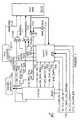
- FIG. 1Ashows a block diagram of a storage system used according to one aspect of the present invention
- FIG. 1Bis a block diagram of a buffer controller, used according to one aspect of the present invention.
- FIG. 2Ashows the data path between a disk formatter and a buffer memory, according to one aspect of the present invention
- FIG. 2Bshows the data path for Read-Long data, according to one aspect of the present invention
- FIG. 3Ashows a block diagram of conversion logic, according to one aspect of the present invention.
- FIGS. 3 B(i)-(iv)shows a table that aligns data into a shuttle register, according to one aspect of the present invention
- FIG. 3Cshows a schematic of a MUX producing an output, according to one aspect of the present invention
- FIG. 4shows the read path during a buffer read operation, according to one aspect of the present invention
- FIG. 5shows the write path during a buffer read operation, according to one aspect of the present invention
- FIG. 6shows a block diagram for a channel (CH 0 ) that facilitates buffer read and write operations, according to one aspect of the present invention
- FIG. 7shows a schematic of CH 0 control logic with a state machine that interfaces with conversion logic, according to one aspect of the present invention
- FIGS. 8 and 9show the timing diagrams for the various signal for buffer write and read operations, according to one aspect of the present invention.
- FIG. 10shows a process flow diagram for data conversion and alignment, according to one aspect of the present invention.
- the system of FIG. 1Ais an example of a storage drive system (with an optical disk or tape drive), included in (or coupled to) a computer system.
- the host computer(not shown) and the storage device 110 (also referred to herein as disk 110 ) communicate via a port using a disk formatter “DF” 104 .
- the storage device 110is an external storage device, which is connected to the host computer via a data bus.
- the data busfor example, is a bus in accordance with a Small Computer System Interface (SCSI) specification.
- SCSISmall Computer System Interface
- the systemincludes controller 101 , which is coupled to buffer memory 111 and microprocessor 100 .
- Interface 109serves to couple microprocessor bus 107 to microprocessor 100 and a micro-controller 102 .
- a read only memory (“ROM”) omitted from the drawingis used to store firmware code executed by microprocessor 100 .
- Host interface 103 in controller 101interfaces with interface 104 A to communicate with a host system (not shown).
- Controller 101can be an integrated circuit (IC) that comprises of various functional modules, which provide for the writing and reading of data stored on storage device 110 .
- Microprocessor 100is coupled to controller 101 via interface 109 to facilitate transfer of data, address, timing and control information.
- Buffer memory 111is coupled to controller 101 via ports to facilitate transfer of data, timing and address information.
- Buffer memory 111may be a double data rate synchronous dynamic random access memory (“DDR-SDRAM”) or synchronous dynamic random access memory (“SDRAM”), or any other type of memory.
- DDR-SDRAMdouble data rate synchronous dynamic random access memory
- SDRAMsynchronous dynamic random access memory
- Disk formatter 104is connected to microprocessor bus 107 and to buffer controller 108 .
- a direct memory access (“DMA”) DMA interface(not shown) is connected to microprocessor bus 107 and to data and control port (not shown).
- DMAdirect memory access
- Buffer controller 108connects buffer memory 111 , channel one (CH 1 ) 105 , error correction code (“ECC”) module 106 and to microprocessor bus 107 .
- Buffer controller 108regulates data movement into and out of buffer memory 111 .
- ECC module 106generates the ECC that is saved on disk 110 writes and provides correction mask to BC 108 for disk 110 read operation.
- Plural channelsmay be used to allow data flow.
- Channelsfor example, channel 0 (“CH 0 ”), channel 1 (“CH 1 ”) and channel 2 (“CH 2 ”)
- CH 0 ”channel 0
- CH 1channel 1
- CH 2channel 2
- CH 1 105may be inside BC 108 or outside BC 108 , as shown in FIG. 1 .
- Another channel (CH 2 )may also be provided so that controller 101 can be used with different systems.
- Firmware running on microprocessor 100can access the channels based on bandwidth and other requirements.
- CH 0 108 D within BC 108can process new symbol based (i.e. 10-bit) data format, according to one aspect of the present invention, as described below.
- a host systemsends a read command to controller 101 , which stores the read commands in buffer memory 111 .
- Microprocessor 100then reads the command out of buffer memory 111 and initializes the various functional blocks of controller 101 .
- Datais read from storage device 110 and is passed to buffer controller 108 .
- a host systemsends a write command to controller 101 and is stored in buffer memory 111 .
- Microprocessor 100reads the command out of buffer memory 111 and sets up the appropriate registers. Data is transferred from the host and is first stored in buffer memory 111 , before being written to disk 110 . CRC values are calculated based on the logical block address (“LBA”) for the sector being written. Data is read out of buffer memory 111 , appended with ECC code and written to disk 110 .
- LBAlogical block address
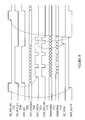
- FIG. 1Bshows a block diagram of BC 108 with CH 0 108 D that interfaces with DF 104 for moving data to and from buffer memory 111 .
- BC 108includes register(s) 108 E and an Arbiter 108 C.
- Arbiter 108 Carbitrates between plural channels in BC 108 , for example, CH 0 108 D, and CH 1 105 and CH 2 (not shown).
- CH 0 108 Dinterfaces with DF 104 , ECC module 106 and a DMA module (not shown).
- Register 108 Eis coupled to interface 109 via bus 107 that allows microprocessor 100 and BC 108 to communicate. Data 108 G and status 108 F is moved in and out of register 108 E. Interface 108 K and 108 L allow BC 108 to interface with CH 1 105 and CH 2 .
- BC 108uses a data wedge format table “DWFT” 108 H to process a data wedge for disk operations.
- DWFTdata wedge format table
- BC 108also includes a memory controller 108 B that interfaces with buffer memory 111 through a synchronous dynamic random access memory (“SDRAM”) interface 108 J or DDR-SDRAM interface 108 A (referred to as DDR-EXT I/F in FIG. 1B ). Interrupts 1081 are sent from buffer controller 108 to microprocessor 100 .
- SDRAMsynchronous dynamic random access memory
- DDR-EXT I/FDDR-EXT I/F in FIG. 1B
- the format of the data in buffer memory 111is still in 8-bit sizes, i.e., byte oriented.
- Table IIshows the format of the data that is stored in buffer memory 111 .
- Datais aligned on a Mod 4 buffer address with a Mod 4 byte size.
- Dataincludes 4 bytes of cyclic redundancy code (“CRC”), if CRC is enabled.
- CRCcyclic redundancy code
- Table II belowassumes a starting address of 0, however, the starting address could be any even multiple of 4.
- Data represented in buffer memory 111is typically the host data block. This data is written and read from disk 110 .
- the host datais in bytes and is written to and read from the disk 110 across a symbol based interface.
- CH 0 108 D logicprovides access to buffer memory 111 with the byte based data format, and access the DF 104 symbol based format, and translates between the two formats, according to one aspect of the present invention, as described below.
- data from disk 110can be in X-bit format and stored in buffer memory 111 in Y-bit format, and CH 0 108 D architecture allows translation between the two formats (i.e. X and Y bit formats).
- FIG. 2Ashows a block diagram with the data path between DF 104 and buffer memory 111 .
- Data 200 as 10-bit symbolsis sent or read from DF 104 via bus 200 A.
- CH 0 FIFO 201is used to store data when it is being transferred between buffer memory 111 and DF 104 .
- Logic 202converts the data format from 10-bit to 8-bit and 8-bit to 10-bit.
- Logic 203receives data to and from buffer 111 and logic 202 .
- Data 204is 8-bit bytes that is received from or sent to buffer memory 111 via bus 204 A.
- Bus 202 Ais 80-bit wide and 202 B is 64-bit wide.
- Buffer Memory 111Read Operations:
- CH 0 logic 203reads data from interface 108 J or 108 A (may be referenced interchangeably as interface 108 J) and passes the data to logic 202.
- Logic 202assembles 80-bit words to write into CH 0 FIFO 201 .
- the last symbol that is written into CH 0 FIFO 201includes pad bits if the transfer size length in bits (plus CRC bits) is not MOD 10 .
- Filler bitsmay also be used to achieve MOD 8 symbol size on a last FIFO write, as described below. “MOD” in this context, as used throughout this specification, means the data alignment.
- Buffer Memory 111Write Operations:
- Buffer write operationinvolves moving data from DF 104 (as shown in FIG. 2A ) to buffer memory 111 .
- Datais first written into CH 0 FIFO 201 beginning at the even MOD- 4 boundary (i.e. the start of a CH 0 FIFO word).
- CH 0 108 Daligns data from DF 104 so that the first data block is written into CH 0 FIFO 201 with even MOD 4 boundary.
- Logic 202then reads 8 symbols at a time and assembles data into an 8-bit MOD- 4 format. This conversion removes even symbol boundary (“ESB”) pad bits, if any, that were appended to the last data symbol ( FIG. 2B ).
- ESDeven symbol boundary
- CH 0 108 Ddoes not remove ESB pad bits, since all data from disk 110 is sent to buffer memory 111 .
- FIG. 2Bshows the data path for Read-Long data.
- ESB pad bits 208 and MOD- 4 pad bits 207are sent with the data to CH 0 FIFO 201 .
- Data that is sent into buffer memory 111is shown as 205 and 206 .
- Block 205includes data and CRC, while block 206 includes ESB pad bits and the ECC.
- FIG. 3Ashows a block diagram of logic 202 , according to one aspect of the present invention.
- Logic 202interfaces to a 64-bit bus 204 A on one side and 80-bit bus 202 A on another side.
- Logic 202uses DATAIN register 303 , shuttle register 305 and DATAOUT register 309 to perform bus width conversions.
- Data that is read from buffer memory 111is shown as 300 .
- Data that is written to buffer memory 111is shown as 301 that is stored in CH 0 FIFO 201 before being written.
- DATAIN register 303receives data 300 from buffer memory 111 or CH 0 FIFO data 301 through a multiplexer (“Mux”) 307 . Thereafter, register 303 provides data to conversion logic. In one aspect of the present invention, DATAIN register 303 is 10 bytes wide during a read operation. It is noteworthy that the present invention is not limited to any particular size of any of the registers that are described herein.
- Buffer write signal 302provides a control input to Mux 307 so that data can be written to buffer memory 111 .
- Shuttle register 305holds data temporarily before it is sent out to DATAOUT register 309 .
- Shuttle register 305uses shuttle Mux 304 to concatenate data that is received from “DATAIN register” 303 with data that is being held in shuttle register 305 .
- a counter 306counts the number of valid data bytes in shuttle register 305 .
- FIG. 3Bshows a table that illustrates how Mux 304 aligns data into the shuttle register 305 .
- the tableis divided in two parts, one for a write operation and another for a read operation. The following describes the various column headings that are used in FIG. 3B table:
- Buffer memory 111 write operationsstart from low word.
- buffer memory write 111only 8 bytes are used and hence d 08 and d 09 columns are not used, as shown in FIG. 3B table.
- FIFO data 301is in 10 bytes and data from DATAOUT register 309 is 8 bytes.
- each time FIFO data 301 is readthere is a remainder of 2 bytes. This remainder of 2 bytes is stored and accumulated in shuttle register 305 .
- shuttle register 305 datais written into DATAOUT register 309 without reading FIFO data 301 . This is shown as overflow entry 312 in FIG. 3B .
- logic 202 using the shuttle mechanismcan start or end in either D-word of the 64 bit bus 204 A. Since sector size is MOD 4 , only 4 or 8 bytes are used.
- FIG. 3Cshows a schematic of MUX 304 , with inputs 304 A and 304 B producing output 304 C. Signals In_Datain, In_Shuttle, Word_Select and Buffer_Write have been described above with respect to FIG. 3B .
- Tables III-V belowshow the byte count present at three stages and the progress of the residue (i.e., last byte in shuttle register 305 ) left in shuttle register 305 .
- the illustrationis based on when the read operation starts at an odd D_word boundary and ends in an Odd D_word boundary (Table III), starts on an odd boundary but ends in an even boundary (Table IV), and then starts on an even boundary and ends in an odd boundary (Table V).
- Tables III and IVshow the first cycle with 4 bytes where a transfer of data from buffer 111 starts on the odd D-Word boundary. Tables III and IV also show 4 bytes on the last cycle where BC interface 108 J is able to end on a single D-Word transfer. The highest byte count in shuttle register 305 is still 8 bytes.
- DATAOUT register 309holds data before it is moved out.
- DATAOUT registeris 10 bytes wide and only 8 bytes are used for buffer memory 111 write operations.
- “DATAOUT register” 309is written when shuttle register 305 and the number of bytes in DATAIN register 303 is equal to the bus width needed for the operation (i.e., 10 bytes during buffer memory 111 read and 8 bytes during buffer memory 111 write).
- Mux 308is used to align data into the proper bus width. (See FIG. 3B table).
- PaddingIf the length of a data block is not MOD 10 , then padding may be used on the last symbol so that it can be written in CH 0 FIFO 201 .
- the pad bitsallow ECC insertion at ESB.
- Logic 202removes the ESB pad bits during buffer memory 111 write operations. ESB pad bits are not removed during Read-Long commands as raw data from DF 104 is sent to buffer memory 111 (see FIG. 2B ).
- Filler bitsare bits that are added at the end of a FIFO word, but are not sent to disk 110 .
- Logic 202accesses CH 0 FIFO 201 8 symbols at a time. This allows writing the first symbol of a transfer into even MOD 4 boundary of CH 0 FIFO 201 (at the beginning of a FIFO word). If data transfer length is not MOD 8 symbols, the last CH 0 FIFO 201 write is accompanied by filler strobes to CH 0 FIFO 201 , if needed, at the end of disk reads.
- Logic 202uses a counter 201 G ( FIG. 6 ) to stop data conversion at a sector boundary.
- Counter 201 Gloads the sector size in bytes from a transfer counter register (not shown) and logic 202 accesses data 301 .
- Counter 201 Gis decremented by 10 for each access (10 byte access) and when FIFO sector count is zero, the conversion by logic 202 stops. Conversion resumes when state machine 203 A sends a signal.
- logic 202packs data from a 64-bit bus 204 A into an 80-bit bus 202 A.
- Shuttle register 305is used to store data temporarily.
- Data 300 from buffer memory 111comes into “DATAIN register” 303 and then shuttle register 305 data and “DATAIN register” 303 data is concatenated and assembled into an 80-bit bus 202 A.
- FIG. 4shows the read path 400 during buffer memory 111 read operation. Data moves from buffer memory 111 to register 311 .
- Table VI belowshows the byte count present during the operation.
- “DATAOUT register” 309is written when Bytes_IN_Dataln (register 303 bytes) and BYTES_IN_Shuttle (data in shuttle register 305 ) reach a count of 10 or more.
- the last row in Table VIshows that 6 bytes are left in shuttle register 305 .
- Logic 202uses FIFO sector counter 201 G to detect the end of the sector and force the residual shuttle bytes into CH 0 FIFO 201 . Firmware can also force the residue into CH 0 FIFO 201 .
- logic 202unpacks 80-bit bus 202 A data into 64-bit bus 204 A data.
- FIFO data 301enters “DATAIN register” 303 .
- Data from shuttle register 305 and “DATAIN register” 303are concatenated and assembled into 64-bit bus 204 data.
- “DATAOUT register” 309writes into register 310 , 8 bytes at a time.
- FIG. 5shows the data path 500 for the write operation.
- Table VII belowshows the byte count during the write operation.
- Register 310is provided 8 bytes of data continuously to avoid delay.
- FIFO data 301is not read when shuttle register 305 count reaches 8, as discussed above.
- Table VIIshows a byte count table for data 301 movement to register 310 .
- FIG. 6shows another block diagram for CH 0 108 D that facilitates buffer memory 111 read and write operations.
- Control logic 203interacts with buffer memory 111 and DF 104 through interfaces 602 , 108 J and 601 .
- Control information 607 , 608 and 609is passed between logic 203 , DF 104 , buffer memory 111 and ECC module 106 .
- CH 0 FIFO 201includes memory (“RAM”) 201 D that is used to store data blocks.
- RAMrandom access memory
- the term FIFO as used throughout this specificationmeans “first-in-first out”.
- Data 201 E(on 80 bit bus 202 A) is passed to logic 202 as discussed above.
- Data 604 from logic 202leaves on a 64-bit bus 203 B (see FIG. 2A ).
- CRC module 603provides CRC data when needed. It is noteworthy that CH 0 FIFO 201 throughout this specification means the entire module that includes memory 201 D.
- FIG. 7shows a detailed schematic of CH 0 control logic 203 with a state machine 203 A that interfaces with logic 202 .
- Data path 700has been described above. The following provides a description of various signals that are used in FIG. 7 to accomplish the adaptive aspects of the present invention:
- Signal 701(CH 0 _SHUT_EN) enables the shuttle function in CH 0 108 H and allows byte to symbol translation, as described above.
- logic 202is disabled and logic 203 accesses CH 0 FIFO 201 as a 64 bit wide FIFO.
- Signal 702(SM_SHUT_GO) is generated by state machine 203 A and when active indicates that logic 202 should start processing data. This signal is set active when state machine 203 A is ready to process a next sector and set inactive once data transfer begins between logic 202 and interface 108 J.
- Signal 703(CH 0 _BUFFER_WR): This signal is generated from state machine 203 A and indicates the transfer direction for data movement (i.e. from to buffer memory 111 or from buffer memory 111 ). When signal 701 is high it indicates that data moves from DF 104 to buffer memory 111 .
- Signal 704(SM_DATA_EN) is driven by state machine 203 A and is the data transfer strobe for accessing logic 202 / CH 0 FIFO 201 . Data is transferred each clock this signal is active (high).
- Signal 705(SM_FIFO_WR) is used by state machine 203 A during logic 202 bypass mode to write to FIFO RAM 201 D.
- Signal 706originates from logic 202 and is sent to state machine 203 A.
- Signal 706is used to hold off state machine 203 A from starting buffer memory 111 data bursts until logic 202 is ready to start executing data transfers.
- signal 706is high during disk 110 read, it indicates that shuttle register 305 is empty and state machine 203 A may not start a current sector since no data is available for buffer memory 111 .
- signal 706indicates that logic 202 is still busy on a current sector and the state 203 A may not start the protocol for the next sector.
- Signal 707(SHUT_DATEN) is also driven by logic 202 to access CH 0 FIFO 201 .
- signal 707indicates an access to 201 D.
- FIFO counter 201 Aincrements by one on disk 110 write decrement on disk reads.
- Signal 708(CH 0 —FIFO _DOUT) is driven from logic 202 when enabled to provide byte alignment, as described above.
- Signal 709(CH 0 —FIFO _DIN) is the data driven from data path logic 700 (located at interface 108 J) and is sent to logic 202 for conversion, as described above.
- Signal 710(SHUT_FIFO_WR) is generated by logic 202 for FIFO 201 write.
- Signal 711is generated from Mux 711 A and sent to FIFO RAM 201 D.
- Signal (RAMDIN) 712is data in to FIFO RAM 201 D and signal (RAMDOUT) 713 is data out from FIFO RAM 201 D to the data path logic 700 .
- Signal (SHUT DOUT) 714is the data out from logic 202 .
- Signal (RAMADR) 715is the RAM address from counters 201 A.
- Signals 716are various error correction signals that are received by state machine 203 A and logic 202 .
- Counter(s) 201 Acounts CH 0 FIFO 201 entries.
- the value in counter 201 Arepresents CH 0 FIFO 201 half words that have been written and not yet read.
- FIGS. 8 and 9show the timing diagrams for the various signals (that are described above with respect to FIG. 7 ) for buffer memory 111 write and read operations, respectively.
- Signal TSC_TERMdefines the time when FIFO sector count is zero.
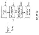
- FIG. 10shows a process flow diagram of executable process steps, according to one aspect of the present invention.
- the processreceives data. If data is being written to buffer memory 111 , then data is received from DF 104 to CH 0 FIFO 201 , otherwise data is received by CH 0 FIFO 201 from buffer memory 111 .
- step S 1001the process determines if any format conversion is required. This is based on the data format supported by the storage device 110 . For example, if data is coming from a tape drive ( 110 ), then no conversion is required and data is processed as 8-bit data in step S 1004 . If data is coming from a hard disk ( 110 ) that operates in a 10-bit format (or a format different from buffer memory 111 ), then conversion is required and logic 202 is enabled. This is achieved by signal 701 that is generated by state machine 203 a ( FIG. 7 ).
- step S 1003data is aligned by logic 202 .
- datais being written from DF 104 , then data is received in 10-bit format.
- Data from CH 0 FIFO 201is stored in shuttle register 305 and sent over bus 204 A.
- Shuttle register 305paces data transfer from CH 0 FIFO 201 to avoid an overflow condition ( FIG. 3B ).
- logic 202moves the 8-bit data to a 10-bit format.
- Logic 202is capable of moving data through buses with varying widths (bus 202 A and 203 A).
- step S 1003data is transferred after the conversion logic 202 has aligned the data based on storage device 110 and buffer memory 111 format requirements.
- same piece of logicis used to move data to and from buffer 111 in two different formats. This saves overall chip cost and improves data transfer performance.
Landscapes
- Engineering & Computer Science (AREA)
- Theoretical Computer Science (AREA)
- Human Computer Interaction (AREA)
- Physics & Mathematics (AREA)
- General Engineering & Computer Science (AREA)
- General Physics & Mathematics (AREA)
- Bus Control (AREA)
- Signal Processing For Digital Recording And Reproducing (AREA)
Abstract
Description
| TABLE I | |
| Symbol | Bit Number |
| No. | 9 | 8 | 7 | 6 | 5 | 4 | 3 | 2 | 1 | 0 |
| 0 | B1-1 | B1-0 | B0-7 | B0-6 | B0-5 | B0-4 | B0-3 | B0-2 | B0-1 | B0-0 |
| 1 | B2-3 | B2-2 | B2-1 | B2-0 | B1-7 | B1-6 | B1-5 | B1-4 | B1-3 | B1-2 |
| 2 | B3-5 | B3-4 | B3-3 | B3-2 | B3-1 | B3-0 | B2-7 | B2-6 | B2-5 | B2-4 |
| 3 | B4-7 | B4-6 | B4-5 | B4-4 | B4-3 | B4-2 | B4-1 | B4-0 | B3-7 | B3-6 |
| TABLE II | ||
| Dword | Bit | Buffer |
| Number | BD[31:24] | BD{23:16] | BD[15:8] | BD[7:0] | ||
| 0 | B3 | B1 | B0 | 0 | ||
| 1 | B7 | B6 | B5 | B4 | 3 | |
| . | . | . | . | . | . | |
| . | . | . | . | . | . | |
| . | . | . | . | . | . | |
| DWn-1 | Bn | Bn-1 | Bn-2 | Bn-3 | (DWn-1 × | |
| 4) − 1 | ||||||
| DWn | CRC-B3 | CRC-B2 | CRC-B1 | CRC-B0 | (DWn × | |
| 4) − 1 | ||||||
| TABLE III |
| BC Odd-Start, Odd-End |
| BYTES_IN_SHUTTLE | BYTES_IN_DataOut | ||
| 4 | 0 | 0 |
| 8 | 4 | 0 |
| 8 | 2 | 10 |
| 8 | 0 | 10 |
| 8 | 8 | 0 |
| 8 | 6 | 10 |
| 8 | 4 | 10 |
| 4 | 2 | 10 |
| 0 | 6 | 0 |
| TABLE IV |
| BC Odd-Start, Even-End |
| BYTES_IN_SHUTTLE | BYTES_IN_DataOut | ||
| 4 | 0 | 0 |
| 8 | 4 | 0 |
| 8 | 2 | 10 |
| 8 | 0 | 10 |
| 8 | 8 | 0 |
| 8 | 6 | 10 |
| 8 | 4 | 10 |
| 0 | 2 | 10 |
| TABLE V |
| BC Even-Start, Odd-End |
| BYTES_IN_SHUTTLE | BYTES_IN_DataOut | ||
| 8 | 0 | 0 |
| 8 | 8 | 0 |
| 8 | 6 | 10 |
| 8 | 4 | 10 |
| 8 | 2 | 10 |
| 4 | 0 | 10 |
| 0 | 4 | 0 |
| TABLE VI |
| Even_Start, Even End |
| BYTES_IN_SHUTTLE | BYTES_IN_DataOut | ||
| 8 | 0 | 0 |
| 8 | 8 | 0 |
| 8 | 6 | 10 |
| 8 | 4 | 10 |
| 8 | 2 | 10 |
| 8 | 0 | 10 |
| 8 | 8 | 0 |
| 8 | 6 | 10 |
| 8 | 4 | 10 |
| 8 | 2 | 10 |
| 8 | 0 | 10 |
| 8 | 8 | 0 |
| 0 | 6 | 10 |
| TABLE VII | |||
| BYTES_IN_SHUTTLE | BYTES_IN_DataOut | ||
| 10 | 0 | 0 |
| 10 | 2 | 8 |
| 10 | 4 | 8 |
| 10 | 6 | 8 |
| 0 | 8 | 8 |
| 10 | 0 | 8 |
| 10 | 2 | 8 |
| 10 | 4 | 8 |
| 10 | 6 | 8 |
| 0 | 8 | 8 |
| 10 | 0 | 8 |
| 10 | 2 | 8 |
| 10 | 4 | 8 |
| 10 | 6 | 8 |
| 0 | 8 | 8 |
| 10 | 0 | 8 |
| 10 | 2 | 8 |
| 10 | 4 | 8 |
Claims (20)
Priority Applications (1)
| Application Number | Priority Date | Filing Date | Title |
|---|---|---|---|
| US10/878,803US8166217B2 (en) | 2004-06-28 | 2004-06-28 | System and method for reading and writing data using storage controllers |
Applications Claiming Priority (1)
| Application Number | Priority Date | Filing Date | Title |
|---|---|---|---|
| US10/878,803US8166217B2 (en) | 2004-06-28 | 2004-06-28 | System and method for reading and writing data using storage controllers |
Publications (2)
| Publication Number | Publication Date |
|---|---|
| US20050289261A1 US20050289261A1 (en) | 2005-12-29 |
| US8166217B2true US8166217B2 (en) | 2012-04-24 |
Family
ID=35507406
Family Applications (1)
| Application Number | Title | Priority Date | Filing Date |
|---|---|---|---|
| US10/878,803Expired - Fee RelatedUS8166217B2 (en) | 2004-06-28 | 2004-06-28 | System and method for reading and writing data using storage controllers |
Country Status (1)
| Country | Link |
|---|---|
| US (1) | US8166217B2 (en) |
Cited By (3)
| Publication number | Priority date | Publication date | Assignee | Title |
|---|---|---|---|---|
| WO2021025864A1 (en)* | 2019-08-05 | 2021-02-11 | Cypress Semiconductor Corporation | Methods for error detection and correction and corresponding systems and devices for the same |
| US11467771B2 (en)* | 2017-01-31 | 2022-10-11 | Christopher V. Beckman | Data storage with reference to an auxiliary pattern |
| US20230030591A1 (en)* | 2013-03-15 | 2023-02-02 | Christopher V. Beckman | Data Storage Device Using an External Reference Pattern |
Families Citing this family (5)
| Publication number | Priority date | Publication date | Assignee | Title |
|---|---|---|---|---|
| US7836247B2 (en)* | 2004-12-17 | 2010-11-16 | International Business Machines Corporation | Method, apparatus, and computer program product for permitting access to a storage drive while the drive is being formatted |
| US8572302B1 (en)* | 2006-10-13 | 2013-10-29 | Marvell International Ltd. | Controller for storage device with improved burst efficiency |
| US7924521B1 (en)* | 2007-04-10 | 2011-04-12 | Marvell International Ltd. | Data wedge format table synchronization |
| US10522237B2 (en) | 2015-08-07 | 2019-12-31 | Mentor Graphics Corporation | Low power VLSI designs using circuit failure in sequential cells as low voltage check for limit of operation |
| CN116189729A (en)* | 2022-09-05 | 2023-05-30 | 长江存储科技有限责任公司 | Memory operation method, memory and memory system |
Citations (198)
| Publication number | Priority date | Publication date | Assignee | Title |
|---|---|---|---|---|
| US3800281A (en) | 1972-12-26 | 1974-03-26 | Ibm | Error detection and correction systems |
| US3988716A (en) | 1974-08-05 | 1976-10-26 | Nasa | Computer interface system |
| US4001883A (en) | 1974-03-07 | 1977-01-04 | Honeywell Information Systems, Inc. | High density data storage on magnetic disk |
| US4016368A (en) | 1975-12-12 | 1977-04-05 | North Electric Company | Framing circuit for digital receiver |
| US4050097A (en) | 1976-09-27 | 1977-09-20 | Honeywell Information Systems, Inc. | Synchronization technique for data transfers over an asynchronous common bus network coupling data processing apparatus |
| US4080649A (en) | 1976-12-16 | 1978-03-21 | Honeywell Information Systems Inc. | Balancing the utilization of I/O system processors |
| US4156867A (en) | 1977-09-06 | 1979-05-29 | Motorola, Inc. | Data communication system with random and burst error protection and correction |
| US4225960A (en) | 1979-03-01 | 1980-09-30 | Westinghouse Electric Corp. | Automatic synchronizing system for digital asynchronous communications |
| US4275457A (en) | 1977-05-18 | 1981-06-23 | Martin Marietta Corporation | Apparatus and method for receiving digital data at a first rate and outputting the data at a different rate |
| US4390969A (en) | 1980-04-21 | 1983-06-28 | Burroughs Corporation | Asynchronous data transmission system with state variable memory and handshaking protocol circuits |
| US4451898A (en) | 1981-11-09 | 1984-05-29 | Hewlett-Packard Company | Asynchronous interface message transmission using source and receive devices |
| US4486750A (en) | 1981-05-18 | 1984-12-04 | Takeda Riken Co. Ltd. | Data transfer system |
| US4500926A (en) | 1981-06-17 | 1985-02-19 | Tokyo Shibaura Denki Kabushiki Kaisha | Data-recording apparatus |
| US4517552A (en)* | 1981-05-26 | 1985-05-14 | Sony Corporation | Method and apparatus for N-to-M encoding |
| US4587609A (en) | 1983-07-01 | 1986-05-06 | Honeywell Information Systems Inc. | Lockout operation among asynchronous accessers of a shared computer system resource |
| US4603382A (en) | 1984-02-27 | 1986-07-29 | International Business Machines Corporation | Dynamic buffer reallocation |
| US4625321A (en) | 1985-05-23 | 1986-11-25 | Standard Microsystems Corporation | Dual edge clock address mark detector |
| US4667286A (en) | 1984-12-20 | 1987-05-19 | Advanced Micro Devices, Inc. | Method and apparatus for transferring data between a disk and a central processing unit |
| US4719523A (en)* | 1985-05-28 | 1988-01-12 | Sony Corporation | Synchronizing signal detecting circuit |
| US4750149A (en)* | 1986-07-03 | 1988-06-07 | Integrated Device Technology, Inc. | Programmable FIFO buffer |
| US4777635A (en) | 1986-08-08 | 1988-10-11 | Data Systems Technology Corp. | Reed-Solomon code encoder and syndrome generator circuit |
| US4805046A (en) | 1985-10-28 | 1989-02-14 | Matsushita Electric Industrial Co., Ltd. | Information recording and reproducing apparatus using sectors divided into a plurality of frames and having means for proper storage of the frame data |
| US4807253A (en) | 1987-11-13 | 1989-02-21 | American Telephone And Telegraph Company, At&T Bell Laboratories | Time-varying trellis-coded modulation formats which are robust in channels with phase variations |
| US4807116A (en) | 1976-09-07 | 1989-02-21 | Tandem Computers Incorporated | Interprocessor communication |
| US4809091A (en) | 1986-04-16 | 1989-02-28 | Hitachi, Ltd. | Disk apparatus |
| US4811282A (en) | 1985-12-18 | 1989-03-07 | Sgs Mircroelettronica Spa | Retiming circuit for pulse signals, particularly for microprocessor peripherals |
| US4812769A (en) | 1986-04-30 | 1989-03-14 | Tektronix, Inc. | Programmable sampling time base circuit |
| US4860333A (en) | 1986-03-12 | 1989-08-22 | Oread Laboratories, Inc. | Error protected central control unit of a switching system and method of operation of its memory configuration |
| US4866606A (en) | 1984-06-22 | 1989-09-12 | Austria Miktosystem International Gmbh | Loosely coupled distributed computer system with node synchronization for precision in real time applications |
| US4866601A (en)* | 1987-09-24 | 1989-09-12 | Ncr Corporation | Digital data bus architecture for computer disk drive controller |
| US4881232A (en) | 1987-02-10 | 1989-11-14 | Sony Corporation | Method and apparatus for error correction |
| US4920535A (en) | 1987-12-14 | 1990-04-24 | Fujitsu Limited | Demultiplexer system |
| US4947410A (en)* | 1989-02-23 | 1990-08-07 | General Motors Corporation | Method and apparatus for counting with a nonvolatile memory |
| US4949342A (en) | 1987-04-14 | 1990-08-14 | Matsushita Electric Industrial Co., Ltd. | Code error detecting method |
| EP0383437A2 (en)* | 1989-02-14 | 1990-08-22 | Data General Corporation | Format converter |
| US4970418A (en) | 1989-09-26 | 1990-11-13 | Apple Computer, Inc. | Programmable memory state machine for providing variable clocking to a multimode memory |
| US4972417A (en) | 1988-06-24 | 1990-11-20 | Sony Corporation | PCM data transmitting apparatus and method |
| US4975915A (en) | 1987-04-19 | 1990-12-04 | Sony Corporation | Data transmission and reception apparatus and method |
| US4989190A (en) | 1987-07-20 | 1991-01-29 | Oki Electric Industry Co., Ltd. | Apparatus for seeking a track of an optical disk in which information is recorded |
| US5014186A (en) | 1986-08-01 | 1991-05-07 | International Business Machines Corporation | Data-processing system having a packet transfer type input/output system |
| US5023612A (en) | 1989-07-13 | 1991-06-11 | Pacific Bell | Illegal sequence detection and protection circuit |
| US5027357A (en) | 1988-10-14 | 1991-06-25 | Advanced Micro Devices, Inc. | ECC/CRC error detection and correction system |
| US5050013A (en) | 1989-12-04 | 1991-09-17 | Seagate Technology, Inc. | Hard sectoring circuit and method for a rotating disk data storage device |
| US5051998A (en) | 1988-06-28 | 1991-09-24 | Matsushita Electric Industrial Co., Ltd. | Data block deinterleaving and error correction system |
| US5068755A (en) | 1990-06-01 | 1991-11-26 | Micropolis Corporation | Sector pulse generator for hard disk drive assembly |
| US5068857A (en) | 1988-09-02 | 1991-11-26 | Mitsubishi Denki Kabushiki Kaisha | Error correction circuit |
| US5072420A (en) | 1989-03-16 | 1991-12-10 | Western Digital Corporation | FIFO control architecture and method for buffer memory access arbitration |
| US5088093A (en) | 1986-04-18 | 1992-02-11 | Cias, Inc. | Self-correcting registers, error-detecting/correcting registers, and inversion coding using one bit, and other information storage media |
| US5109500A (en) | 1986-10-31 | 1992-04-28 | Hitachi, Ltd. | Disk drive control unit having sets of operating command and operation length information and generating end signal based upon operation length information |
| US5117442A (en) | 1988-12-14 | 1992-05-26 | National Semiconductor Corporation | Methods and circuits for synchronizing signals in a modular redundant fault tolerant computer system |
| US5127098A (en) | 1989-04-12 | 1992-06-30 | Sun Microsystems, Inc. | Method and apparatus for the context switching of devices |
| US5133062A (en) | 1986-03-06 | 1992-07-21 | Advanced Micro Devices, Inc. | RAM buffer controller for providing simulated first-in-first-out (FIFO) buffers in a random access memory |
| US5136592A (en) | 1989-06-28 | 1992-08-04 | Digital Equipment Corporation | Error detection and correction system for long burst errors |
| US5146585A (en) | 1988-10-25 | 1992-09-08 | International Business Machines Corporation | Synchronized fault tolerant clocks for multiprocessor systems |
| US5157669A (en) | 1988-10-14 | 1992-10-20 | Advanced Micro Devices, Inc. | Comparison of an estimated CRC syndrome to a generated CRC syndrome in an ECC/CRC system to detect uncorrectable errors |
| US5162954A (en) | 1990-07-31 | 1992-11-10 | Seagate Technology Inc. | Apparatus for generating an index pulse in a data storage system |
| US5193197A (en) | 1987-09-24 | 1993-03-09 | Digital Equipment Corporation | Apparatus and method for distributed dynamic priority arbitration for access to a shared resource |
| US5204859A (en) | 1990-02-23 | 1993-04-20 | Gec Plessey Telecommunications Limited | Method and apparatus for detecting a frame alignment word in a data system |
| US5218564A (en) | 1991-06-07 | 1993-06-08 | National Semiconductor Corporation | Layout efficient 32-bit shifter/register with 16-bit interface |
| US5220569A (en) | 1990-07-09 | 1993-06-15 | Seagate Technology, Inc. | Disk array with error type indication and selection of error correction method |
| US5237593A (en) | 1989-05-04 | 1993-08-17 | Stc, Plc | Sequence synchronisation |
| US5243471A (en) | 1991-01-10 | 1993-09-07 | Hewlett-Packard Company | Method and apparatus for detecting a start of data position in differing tracks |
| US5249271A (en) | 1990-06-04 | 1993-09-28 | Emulex Corporation | Buffer memory data flow controller |
| US5257143A (en) | 1991-01-15 | 1993-10-26 | Zenith Data Systems Corporation | Method and apparatus for positioning head of disk drive using zone-bit-recording |
| US5261081A (en) | 1990-07-26 | 1993-11-09 | Ncr Corporation | Sequence control apparatus for producing output signals in synchronous with a consistent delay from rising or falling edge of clock input signal |
| US5271018A (en) | 1990-04-27 | 1993-12-14 | Next, Inc. | Method and apparatus for media defect management and media addressing |
| US5274509A (en) | 1992-09-10 | 1993-12-28 | Digital Equipment Corporation | On-the-fly splitting of disk data blocks using timed sampling of a data position indicator |
| US5276564A (en) | 1992-04-16 | 1994-01-04 | Hewlett-Packard Company | Programmable start-of-sector pulse generator for a disk drive using embedded servo bursts and split data fields |
| US5276807A (en) | 1987-04-13 | 1994-01-04 | Emulex Corporation | Bus interface synchronization circuitry for reducing time between successive data transmission in a system using an asynchronous handshaking |
| US5276662A (en) | 1992-10-01 | 1994-01-04 | Seagate Technology, Inc. | Disc drive with improved data transfer management apparatus |
| US5280488A (en) | 1990-11-08 | 1994-01-18 | Neal Glover | Reed-Solomon code system employing k-bit serial techniques for encoding and burst error trapping |
| US5285451A (en) | 1990-04-06 | 1994-02-08 | Micro Technology, Inc. | Failure-tolerant mass storage system |
| US5285327A (en) | 1990-01-17 | 1994-02-08 | International Business Machines Corporation | Apparatus for controlling reading and writing in a disk drive |
| US5301333A (en) | 1990-06-14 | 1994-04-05 | Bell Communications Research, Inc. | Tree structured variable priority arbitration implementing a round-robin scheduling policy |
| US5307216A (en) | 1991-09-04 | 1994-04-26 | International Business Machines Corporation | Sector identification method and apparatus for a direct access storage device |
| US5315708A (en) | 1990-02-28 | 1994-05-24 | Micro Technology, Inc. | Method and apparatus for transferring data through a staging memory |
| US5339443A (en) | 1991-11-19 | 1994-08-16 | Sun Microsystems, Inc. | Arbitrating multiprocessor accesses to shared resources |
| US5361267A (en) | 1992-04-24 | 1994-11-01 | Digital Equipment Corporation | Scheme for error handling in a computer system |
| US5361266A (en) | 1992-11-04 | 1994-11-01 | Mitsubishi Denki Kabushiki Kaisha | Error correction circuit |
| EP0622726A2 (en) | 1993-04-30 | 1994-11-02 | Quantum Corporation | Shared memory array for data block and control program storage in disk drive |
| US5408644A (en) | 1992-06-05 | 1995-04-18 | Compaq Computer Corporation | Method and apparatus for improving the performance of partial stripe operations in a disk array subsystem |
| US5420984A (en) | 1992-06-30 | 1995-05-30 | Genroco, Inc. | Apparatus and method for rapid switching between control of first and second DMA circuitry to effect rapid switching beween DMA communications |
| US5428627A (en)* | 1992-11-10 | 1995-06-27 | Qlogic Corporation | Method and apparatus for initializing an ECC circuit |
| US5440751A (en) | 1991-06-21 | 1995-08-08 | Compaq Computer Corp. | Burst data transfer to single cycle data transfer conversion and strobe signal conversion |
| US5487170A (en) | 1993-12-16 | 1996-01-23 | International Business Machines Corporation | Data processing system having dynamic priority task scheduling capabilities |
| US5488688A (en) | 1994-03-30 | 1996-01-30 | Motorola, Inc. | Data processor with real-time diagnostic capability |
| US5491701A (en) | 1993-11-04 | 1996-02-13 | Cirrus Logic, Inc. | Burst error corrector |
| US5500848A (en) | 1991-07-10 | 1996-03-19 | International Business Machines Corporation | Sector servo data recording disk having data regions without identification (ID) fields |
| US5507005A (en)* | 1991-03-18 | 1996-04-09 | Hitachi, Ltd. | Data transferring system between host and I/O using a main buffer with sub-buffers where quantity of data in sub-buffers determine access requests |
| US5506989A (en) | 1990-01-31 | 1996-04-09 | Ibm Corporation | Arbitration system limiting high priority successive grants |
| US5519837A (en) | 1994-07-29 | 1996-05-21 | International Business Machines Corporation | Pseudo-round-robin arbitration for a shared resource system providing fairness and high throughput |
| US5523903A (en) | 1993-12-23 | 1996-06-04 | International Business Machines Corporation | Sector architecture for fixed block disk drive |
| EP0718827A2 (en) | 1994-12-22 | 1996-06-26 | International Business Machines Corporation | System and method for target track determination in a data storage disk drive |
| US5541908A (en)* | 1993-04-21 | 1996-07-30 | Maxoptix Corporation | Actuator having a minimized payload in a optical recording system |
| US5544346A (en) | 1992-01-02 | 1996-08-06 | International Business Machines Corporation | System having a bus interface unit for overriding a normal arbitration scheme after a system resource device has already gained control of a bus |
| US5544180A (en) | 1992-06-08 | 1996-08-06 | Qlogic Corporation | Error-tolerant byte synchronization recovery scheme |
| US5546545A (en) | 1994-12-09 | 1996-08-13 | International Business Machines Corporation | Rotating priority selection logic circuit |
| US5546548A (en) | 1993-03-31 | 1996-08-13 | Intel Corporation | Arbiter and arbitration process for a dynamic and flexible prioritization |
| US5563896A (en) | 1991-01-22 | 1996-10-08 | Fujitsu Limited | Error correction processor and an error correcting method |
| US5572148A (en) | 1995-03-22 | 1996-11-05 | Altera Corporation | Programmable logic array integrated circuit with general-purpose memory configurable as a random access or FIFO memory |
| US5574867A (en) | 1994-07-08 | 1996-11-12 | Intel Corporation | Fast first-come first served arbitration method |
| US5581715A (en) | 1994-06-22 | 1996-12-03 | Oak Technologies, Inc. | IDE/ATA CD drive controller having a digital signal processor interface, dynamic random access memory, data error detection and correction, and a host interface |
| US5583999A (en) | 1994-01-14 | 1996-12-10 | Fujitsu Limited | Bus arbiter and bus arbitrating method |
| US5592404A (en) | 1993-11-04 | 1997-01-07 | Cirrus Logic, Inc. | Versatile error correction system |
| US5600662A (en) | 1993-09-21 | 1997-02-04 | Cirrus Logic, Inc. | Error correction method and apparatus for headers |
| US5623672A (en) | 1994-12-23 | 1997-04-22 | Cirrus Logic, Inc. | Arrangement and method of arbitration for a resource with shared user request signals and dynamic priority assignment |
| US5627695A (en) | 1995-01-12 | 1997-05-06 | Qlogic Corporation | System and method for generating unique sector identifiers for an identificationless disk format |
| US5629949A (en) | 1993-09-21 | 1997-05-13 | Cirrus Logic, Inc. | Error correction verification method and apparatus using CRC check remainders |
| US5640602A (en) | 1994-06-10 | 1997-06-17 | Fujitsu Limited | Transferring digital data in units of 2 bytes to increase utilization of a 2-byte-wide bus |
| US5649230A (en) | 1992-03-31 | 1997-07-15 | Seiko Epson Corporation | System for transferring data using value in hardware FIFO'S unused data start pointer to update virtual FIFO'S start address pointer for fast context switching |
| US5664121A (en) | 1995-11-07 | 1997-09-02 | Sun Microsystems, Inc. | Dual mode arbitration apparatus and method for reducing latency by allowing the possibility of simultaneous request and access for a shared bus |
| GB2285166B (en) | 1993-12-23 | 1997-10-22 | Ibm | System and method for skip-sector mapping in a data recording disk drive |
| US5689656A (en) | 1995-05-03 | 1997-11-18 | Apple Computer, Inc. | Dynamic hierarchical arbitration of computer resource access requests |
| US5692135A (en) | 1995-12-14 | 1997-11-25 | International Business Machines Corporation | Method and system for performing an asymmetric bus arbitration protocol within a data processing system |
| US5692165A (en) | 1995-09-12 | 1997-11-25 | Micron Electronics Inc. | Memory controller with low skew control signal |
| US5691994A (en) | 1995-05-08 | 1997-11-25 | Western Digital Corporation | Disk drive with fast error correction validation |
| US5719516A (en) | 1995-12-20 | 1998-02-17 | Advanced Micro Devices, Inc. | Lock generator circuit for use with a dual edge register that provides a separate enable for each use of an input clock signal |
| US5729718A (en) | 1993-11-10 | 1998-03-17 | Quantum Corporation | System for determining lead time latency as function of head switch, seek, and rotational latencies and utilizing embedded disk drive controller for command queue reordering |
| US5740466A (en) | 1992-06-26 | 1998-04-14 | Cirrus Logic, Inc. | Flexible processor-driven SCSI controller with buffer memory and local processor memory coupled via separate buses |
| US5745793A (en) | 1995-06-07 | 1998-04-28 | Seagate Technology, Inc. | Apparatus having a circular buffer that maintains a one entry gap between elements written to the microprocessor and elements operated on by the clock |
| US5754759A (en) | 1993-09-29 | 1998-05-19 | U.S. Philips Corporation | Testing and monitoring of programmed devices |
| US5758188A (en) | 1995-11-21 | 1998-05-26 | Quantum Corporation | Synchronous DMA burst transfer protocol having the peripheral device toggle the strobe signal such that data is latched using both edges of the strobe signal |
| US5784569A (en) | 1996-09-23 | 1998-07-21 | Silicon Graphics, Inc. | Guaranteed bandwidth allocation method in a computer system for input/output data transfers |
| US5794073A (en) | 1994-11-07 | 1998-08-11 | Digital Equipment Corporation | Arbitration system for a shared DMA logic on a network adapter with a large number of competing priority requests having predicted latency field |
| US5801998A (en) | 1995-11-06 | 1998-09-01 | Hyundai Electronics Industries Co., Ltd. | Dynamic random access memory |
| US5818886A (en) | 1996-08-22 | 1998-10-06 | Unisys Corporation | Pulse synchronizing module |
| US5822142A (en) | 1996-07-26 | 1998-10-13 | Western Digital Corporation | Method of mapping logical sectors to physical sectors in a disk drive sparing partition |
| US5831922A (en) | 1996-10-22 | 1998-11-03 | Hyundai Electronics Industries Co., Ltd. | Semiconductor device having a refresh device of a noise reduction type |
| US5835930A (en) | 1996-04-09 | 1998-11-10 | International Business Machines Corporation | One or more logical tracks per physical track in a headerless disk drive |
| US5841722A (en) | 1996-02-14 | 1998-11-24 | Galileo Technologies Ltd. | First-in, first-out (FIFO) buffer |
| US5844844A (en) | 1997-07-09 | 1998-12-01 | Xilinx, Inc. | FPGA memory element programmably triggered on both clock edges |
| US5850422A (en) | 1995-07-21 | 1998-12-15 | Symbios, Inc. | Apparatus and method for recovering a clock signal which is embedded in an incoming data stream |
| US5854918A (en) | 1996-01-24 | 1998-12-29 | Ricoh Company Ltd. | Apparatus and method for self-timed algorithmic execution |
| US5864309A (en)* | 1996-10-17 | 1999-01-26 | Winbond Electronics Corp. | Serial data timing base modulator |
| US5887199A (en)* | 1996-06-03 | 1999-03-23 | Emc Corporation | Mass storage controller with universal track size adaptability |
| US5890207A (en) | 1996-11-27 | 1999-03-30 | Emc Corporation | High performance integrated cached storage device |
| US5890210A (en) | 1996-06-28 | 1999-03-30 | Kabushiki Kaisha Toshiba | Magnetic disk apparatus and command processing method thereof |
| US5907717A (en) | 1996-02-23 | 1999-05-25 | Lsi Logic Corporation | Cross-connected memory system for allocating pool buffers in each frame buffer and providing addresses thereof |
| US5912906A (en) | 1997-06-23 | 1999-06-15 | Sun Microsystems, Inc. | Method and apparatus for recovering from correctable ECC errors |
| US5922062A (en)* | 1997-06-26 | 1999-07-13 | Vlsi Technology, Inc. | Combined IDE and SCSI disk controller interface for common hardware reference platforms |
| US5925135A (en) | 1996-09-26 | 1999-07-20 | Intel Corporation | Clock rate compensation for a low frequency slave device |
| US5950223A (en) | 1997-06-19 | 1999-09-07 | Silicon Magic Corporation | Dual-edge extended data out memory |
| US5968180A (en) | 1997-09-30 | 1999-10-19 | Intel Corporation | Data capture circuit for asynchronous data transfer |
| EP0528273B1 (en) | 1991-08-16 | 1999-10-27 | Fujitsu Limited | Buffer memory and method of managing the same |
| US5983293A (en) | 1993-12-17 | 1999-11-09 | Fujitsu Limited | File system for dividing buffer areas into different block sizes for system and user data |
| US5991911A (en) | 1997-11-14 | 1999-11-23 | Cirrus Logic, Inc. | Concurrent generation of ECC error syndromes and CRC validation syndromes in a DVD storage device |
| US6029250A (en) | 1998-09-09 | 2000-02-22 | Micron Technology, Inc. | Method and apparatus for adaptively adjusting the timing offset between a clock signal and digital signals transmitted coincident with that clock signal, and memory device and system using same |
| US6029226A (en) | 1996-09-30 | 2000-02-22 | Lsi Logic Corporation | Method and apparatus having automated write data transfer with optional skip by processing two write commands as a single write command |
| US6041417A (en) | 1998-06-04 | 2000-03-21 | Hewlett-Packard Company | Method and apparatus for synchronizing data received in an accelerated graphics port of a graphics memory system |
| US6065053A (en) | 1997-10-01 | 2000-05-16 | Micron Electronics, Inc. | System for resetting a server |
| US6067206A (en) | 1997-11-18 | 2000-05-23 | Western Digital Corporation | Method and apparatus to compensate for servo wedge rotational offset after a head switch |
| US6070200A (en) | 1998-06-02 | 2000-05-30 | Adaptec, Inc. | Host adapter having paged data buffers for continuously transferring data between a system bus and a peripheral bus |
| US6076120A (en)* | 1997-02-25 | 2000-06-13 | Dainippon Screen Mfg. Co., Ltd. | System for compositing a plurality of pages said pages being classified into three parts each part to be composed in a different data format |
| US6078447A (en) | 1996-10-17 | 2000-06-20 | Samsung Electronics Co., Ltd. | Staggered servo writing method in a hard disk drive employing staggered servo writing |
| US6081849A (en) | 1996-10-01 | 2000-06-27 | Lsi Logic Corporation | Method and structure for switching multiple contexts in storage subsystem target device |
| US6092231A (en) | 1998-06-12 | 2000-07-18 | Qlogic Corporation | Circuit and method for rapid checking of error correction codes using cyclic redundancy check |
| US6094320A (en) | 1995-09-06 | 2000-07-25 | Samsung Electronics Co. Ltd. | Device and method for compensating for interhead track position offset due to the offset of tracks on disk surfaces |
| US6124994A (en) | 1995-12-12 | 2000-09-26 | International Business Machines Corporation | System and method for providing nonadjacent redundancy synchronization bytes |
| US6127948A (en)* | 1998-06-17 | 2000-10-03 | Gurley Precision Instruments, Inc. | Bidirectional synthesis of pseudorandom sequences for arbitrary encoding resolutions |
| US6134063A (en) | 1997-12-30 | 2000-10-17 | Lsi Logic Corporation | Automated multi-track transfers |
| US6157984A (en) | 1997-05-15 | 2000-12-05 | Seagate Technology, Llc | Integrated controller/processor for disc drive having direct memory access |
| US6169501B1 (en)* | 1998-09-23 | 2001-01-02 | National Instruments Corp. | Adjustable serial-to-parallel or parallel-to-serial converter |
| US6178486B1 (en) | 1998-02-19 | 2001-01-23 | Quantum Corporation | Time allocation shared memory arbitration for disk drive controller |
| US6184808B1 (en)* | 1997-09-24 | 2001-02-06 | Nec Corporation | Parallel-to-parallel converter including common multiple register |
| US6192499B1 (en) | 1998-05-29 | 2001-02-20 | Adaptec, Inc. | Device and method for extending error correction beyond one sector time |
| US6201655B1 (en) | 1997-09-19 | 2001-03-13 | Hitachi, Ltd. | Rotational storage device |
| US6223303B1 (en) | 1998-06-29 | 2001-04-24 | Western Digital Corporation | Disk drive having two tiered defect list comprising marginal and reserved data sectors |
| US6237053B1 (en)* | 1998-06-30 | 2001-05-22 | Symbol Technologies, Inc. | Configurable operating system having multiple data conversion applications for I/O connectivity |
| US6279089B1 (en) | 1999-04-12 | 2001-08-21 | Western Digital Technologies, Inc. | Defective data site management through a shared defect management table |
| US6311239B1 (en)* | 1998-10-29 | 2001-10-30 | Cypress Semiconductor Corp. | Architecture, circuitry and method for transmitting n-bit wide data over m-bit wide media |
| US20010044873A1 (en) | 1998-02-27 | 2001-11-22 | Aaron Wade Wilson | Defective data sector management system |
| US6330626B1 (en)* | 1999-05-05 | 2001-12-11 | Qlogic Corporation | Systems and methods for a disk controller memory architecture |
| US6381659B2 (en) | 1999-01-19 | 2002-04-30 | Maxtor Corporation | Method and circuit for controlling a first-in-first-out (FIFO) buffer using a bank of FIFO address registers capturing and saving beginning and ending write-pointer addresses |
| US6401149B1 (en) | 1999-05-05 | 2002-06-04 | Qlogic Corporation | Methods for context switching within a disk controller |
| US20020087746A1 (en)* | 1998-05-08 | 2002-07-04 | Ludtke Harold Aaron | Media manager for controlling autonomous media devices within a network environment and managing the flow and format of data between the devices |
| US6421795B2 (en)* | 1997-07-29 | 2002-07-16 | Nec Corporation | Integrated circuit device and its control method |
| US20020110157A1 (en)* | 2001-02-14 | 2002-08-15 | Kestrel Solutions | Method and apparatus for providing a gigabit ethernet circuit pack |
| US6470461B1 (en) | 1999-06-07 | 2002-10-22 | Qlogic Corporation | Disk drive controller circuit and method for skipping defective and/or undesired sectors |
| US6487631B2 (en) | 1999-02-02 | 2002-11-26 | Qlogic Corporation | Circuit and method for monitoring sector transfers to and from storage medium |
| US6490635B1 (en) | 2000-04-28 | 2002-12-03 | Western Digital Technologies, Inc. | Conflict detection for queued command handling in disk drive controller |
| US6516385B1 (en)* | 1999-01-06 | 2003-02-04 | Hitachi, Ltd. | Data sharing method and system between information processing systems with variable length block format to fixed length block format conversion |
| US20030037225A1 (en) | 2000-12-28 | 2003-02-20 | Deng Brian Tse | Apparatus and method for microcontroller debugging |
| US6529971B1 (en)* | 1998-06-26 | 2003-03-04 | Seagate Technology, Llc | Adaptive elasticity FIFO buffer |
| US6530000B1 (en) | 1999-03-24 | 2003-03-04 | Qlogic Corporation | Methods and systems for arbitrating access to a disk controller buffer memory by allocating various amounts of times to different accessing units |
| US6574676B1 (en) | 2000-01-11 | 2003-06-03 | International Business Machines Corporation | System and method for scheduling disk drive commands by expected total access time |
| US6631131B1 (en)* | 1998-05-13 | 2003-10-07 | Hewlett-Packard Development Company, L.P. | Transpose table biased arbitration scheme |
| US6662334B1 (en) | 1999-02-25 | 2003-12-09 | Adaptec, Inc. | Method and device for performing error correction on ECC data sectors |
| US20040024930A1 (en)* | 1999-12-14 | 2004-02-05 | Shinichi Nakayama | Storage subsystem and storage controller |
| US20040088456A1 (en)* | 2002-10-22 | 2004-05-06 | Guobiao Zhang | Smart hard-disk drive |
| US6826650B1 (en) | 2000-08-22 | 2004-11-30 | Qlogic Corporation | Disk controller configured to perform out of order execution of write operations |
| US20050007811A1 (en)* | 2003-06-04 | 2005-01-13 | Seiji Hyoudou | Storage device and data conversion program |
| US6961832B2 (en)* | 1999-02-19 | 2005-11-01 | Hitachi, Ltd. | Method and system for backing up data of data processing devices including fixed length block format data conversion to variable length block format |
| US7007114B1 (en)* | 2003-01-31 | 2006-02-28 | Qlogic Corporation | System and method for padding data blocks and/or removing padding from data blocks in storage controllers |
| US7047388B2 (en)* | 2002-12-06 | 2006-05-16 | Hitachi, Ltd. | Control method for storage device controller system, and storage device controller system |
| US20060167936A1 (en)* | 2003-03-27 | 2006-07-27 | Osamu Okauchi | Data processing device |
| US7191431B2 (en)* | 2002-12-20 | 2007-03-13 | International Business Machines Corporation | System and method for selecting a translator to translate a component request using semantic typing |
| US7581041B1 (en)* | 2003-12-29 | 2009-08-25 | Apple Inc. | Methods and apparatus for high-speed serialized data transfer over network infrastructure using a different protocol |
| US7752202B2 (en)* | 2002-05-17 | 2010-07-06 | Sony Corporation | Information processing and, content distribution apparatus method, and program with conversion identification information |
Family Cites Families (1)
| Publication number | Priority date | Publication date | Assignee | Title |
|---|---|---|---|---|
| US5626949A (en)* | 1994-04-04 | 1997-05-06 | Blauer Manufacturing Company | Breathable shell for outerwear |
- 2004
- 2004-06-28USUS10/878,803patent/US8166217B2/ennot_activeExpired - Fee Related
Patent Citations (203)
| Publication number | Priority date | Publication date | Assignee | Title |
|---|---|---|---|---|
| US3800281A (en) | 1972-12-26 | 1974-03-26 | Ibm | Error detection and correction systems |
| US4001883A (en) | 1974-03-07 | 1977-01-04 | Honeywell Information Systems, Inc. | High density data storage on magnetic disk |
| US3988716A (en) | 1974-08-05 | 1976-10-26 | Nasa | Computer interface system |
| US4016368A (en) | 1975-12-12 | 1977-04-05 | North Electric Company | Framing circuit for digital receiver |
| US4807116A (en) | 1976-09-07 | 1989-02-21 | Tandem Computers Incorporated | Interprocessor communication |
| US4050097A (en) | 1976-09-27 | 1977-09-20 | Honeywell Information Systems, Inc. | Synchronization technique for data transfers over an asynchronous common bus network coupling data processing apparatus |
| US4080649A (en) | 1976-12-16 | 1978-03-21 | Honeywell Information Systems Inc. | Balancing the utilization of I/O system processors |
| US4275457A (en) | 1977-05-18 | 1981-06-23 | Martin Marietta Corporation | Apparatus and method for receiving digital data at a first rate and outputting the data at a different rate |
| US4156867A (en) | 1977-09-06 | 1979-05-29 | Motorola, Inc. | Data communication system with random and burst error protection and correction |
| US4225960A (en) | 1979-03-01 | 1980-09-30 | Westinghouse Electric Corp. | Automatic synchronizing system for digital asynchronous communications |
| US4390969A (en) | 1980-04-21 | 1983-06-28 | Burroughs Corporation | Asynchronous data transmission system with state variable memory and handshaking protocol circuits |
| US4486750A (en) | 1981-05-18 | 1984-12-04 | Takeda Riken Co. Ltd. | Data transfer system |
| US4517552A (en)* | 1981-05-26 | 1985-05-14 | Sony Corporation | Method and apparatus for N-to-M encoding |
| US4500926A (en) | 1981-06-17 | 1985-02-19 | Tokyo Shibaura Denki Kabushiki Kaisha | Data-recording apparatus |
| US4451898A (en) | 1981-11-09 | 1984-05-29 | Hewlett-Packard Company | Asynchronous interface message transmission using source and receive devices |
| US4587609A (en) | 1983-07-01 | 1986-05-06 | Honeywell Information Systems Inc. | Lockout operation among asynchronous accessers of a shared computer system resource |
| US4603382A (en) | 1984-02-27 | 1986-07-29 | International Business Machines Corporation | Dynamic buffer reallocation |
| US4866606A (en) | 1984-06-22 | 1989-09-12 | Austria Miktosystem International Gmbh | Loosely coupled distributed computer system with node synchronization for precision in real time applications |
| US4667286A (en) | 1984-12-20 | 1987-05-19 | Advanced Micro Devices, Inc. | Method and apparatus for transferring data between a disk and a central processing unit |
| US4625321A (en) | 1985-05-23 | 1986-11-25 | Standard Microsystems Corporation | Dual edge clock address mark detector |
| US4719523A (en)* | 1985-05-28 | 1988-01-12 | Sony Corporation | Synchronizing signal detecting circuit |
| US4805046A (en) | 1985-10-28 | 1989-02-14 | Matsushita Electric Industrial Co., Ltd. | Information recording and reproducing apparatus using sectors divided into a plurality of frames and having means for proper storage of the frame data |
| US4811282A (en) | 1985-12-18 | 1989-03-07 | Sgs Mircroelettronica Spa | Retiming circuit for pulse signals, particularly for microprocessor peripherals |
| US5133062A (en) | 1986-03-06 | 1992-07-21 | Advanced Micro Devices, Inc. | RAM buffer controller for providing simulated first-in-first-out (FIFO) buffers in a random access memory |
| US4860333A (en) | 1986-03-12 | 1989-08-22 | Oread Laboratories, Inc. | Error protected central control unit of a switching system and method of operation of its memory configuration |
| US4809091A (en) | 1986-04-16 | 1989-02-28 | Hitachi, Ltd. | Disk apparatus |
| US5088093A (en) | 1986-04-18 | 1992-02-11 | Cias, Inc. | Self-correcting registers, error-detecting/correcting registers, and inversion coding using one bit, and other information storage media |
| US4812769A (en) | 1986-04-30 | 1989-03-14 | Tektronix, Inc. | Programmable sampling time base circuit |
| US4750149A (en)* | 1986-07-03 | 1988-06-07 | Integrated Device Technology, Inc. | Programmable FIFO buffer |
| US5014186A (en) | 1986-08-01 | 1991-05-07 | International Business Machines Corporation | Data-processing system having a packet transfer type input/output system |
| US4777635A (en) | 1986-08-08 | 1988-10-11 | Data Systems Technology Corp. | Reed-Solomon code encoder and syndrome generator circuit |
| US5109500A (en) | 1986-10-31 | 1992-04-28 | Hitachi, Ltd. | Disk drive control unit having sets of operating command and operation length information and generating end signal based upon operation length information |
| US4881232A (en) | 1987-02-10 | 1989-11-14 | Sony Corporation | Method and apparatus for error correction |
| US5276807A (en) | 1987-04-13 | 1994-01-04 | Emulex Corporation | Bus interface synchronization circuitry for reducing time between successive data transmission in a system using an asynchronous handshaking |
| US4949342A (en) | 1987-04-14 | 1990-08-14 | Matsushita Electric Industrial Co., Ltd. | Code error detecting method |
| US4975915A (en) | 1987-04-19 | 1990-12-04 | Sony Corporation | Data transmission and reception apparatus and method |
| US4989190A (en) | 1987-07-20 | 1991-01-29 | Oki Electric Industry Co., Ltd. | Apparatus for seeking a track of an optical disk in which information is recorded |
| US5193197A (en) | 1987-09-24 | 1993-03-09 | Digital Equipment Corporation | Apparatus and method for distributed dynamic priority arbitration for access to a shared resource |
| US4866601A (en)* | 1987-09-24 | 1989-09-12 | Ncr Corporation | Digital data bus architecture for computer disk drive controller |
| US4807253A (en) | 1987-11-13 | 1989-02-21 | American Telephone And Telegraph Company, At&T Bell Laboratories | Time-varying trellis-coded modulation formats which are robust in channels with phase variations |
| US4920535A (en) | 1987-12-14 | 1990-04-24 | Fujitsu Limited | Demultiplexer system |
| US4972417A (en) | 1988-06-24 | 1990-11-20 | Sony Corporation | PCM data transmitting apparatus and method |
| US5051998A (en) | 1988-06-28 | 1991-09-24 | Matsushita Electric Industrial Co., Ltd. | Data block deinterleaving and error correction system |
| US5068857A (en) | 1988-09-02 | 1991-11-26 | Mitsubishi Denki Kabushiki Kaisha | Error correction circuit |
| US5027357A (en) | 1988-10-14 | 1991-06-25 | Advanced Micro Devices, Inc. | ECC/CRC error detection and correction system |
| US5157669A (en) | 1988-10-14 | 1992-10-20 | Advanced Micro Devices, Inc. | Comparison of an estimated CRC syndrome to a generated CRC syndrome in an ECC/CRC system to detect uncorrectable errors |
| US5146585A (en) | 1988-10-25 | 1992-09-08 | International Business Machines Corporation | Synchronized fault tolerant clocks for multiprocessor systems |
| US5117442A (en) | 1988-12-14 | 1992-05-26 | National Semiconductor Corporation | Methods and circuits for synchronizing signals in a modular redundant fault tolerant computer system |
| EP0383437A2 (en)* | 1989-02-14 | 1990-08-22 | Data General Corporation | Format converter |
| US4947410A (en)* | 1989-02-23 | 1990-08-07 | General Motors Corporation | Method and apparatus for counting with a nonvolatile memory |
| US5072420A (en) | 1989-03-16 | 1991-12-10 | Western Digital Corporation | FIFO control architecture and method for buffer memory access arbitration |
| US5127098A (en) | 1989-04-12 | 1992-06-30 | Sun Microsystems, Inc. | Method and apparatus for the context switching of devices |
| US5237593A (en) | 1989-05-04 | 1993-08-17 | Stc, Plc | Sequence synchronisation |
| US5136592A (en) | 1989-06-28 | 1992-08-04 | Digital Equipment Corporation | Error detection and correction system for long burst errors |
| US5023612A (en) | 1989-07-13 | 1991-06-11 | Pacific Bell | Illegal sequence detection and protection circuit |
| US4970418A (en) | 1989-09-26 | 1990-11-13 | Apple Computer, Inc. | Programmable memory state machine for providing variable clocking to a multimode memory |
| US5050013A (en) | 1989-12-04 | 1991-09-17 | Seagate Technology, Inc. | Hard sectoring circuit and method for a rotating disk data storage device |
| US5285327A (en) | 1990-01-17 | 1994-02-08 | International Business Machines Corporation | Apparatus for controlling reading and writing in a disk drive |
| US5506989A (en) | 1990-01-31 | 1996-04-09 | Ibm Corporation | Arbitration system limiting high priority successive grants |
| US5204859A (en) | 1990-02-23 | 1993-04-20 | Gec Plessey Telecommunications Limited | Method and apparatus for detecting a frame alignment word in a data system |
| US5315708A (en) | 1990-02-28 | 1994-05-24 | Micro Technology, Inc. | Method and apparatus for transferring data through a staging memory |
| US5285451A (en) | 1990-04-06 | 1994-02-08 | Micro Technology, Inc. | Failure-tolerant mass storage system |
| US5271018A (en) | 1990-04-27 | 1993-12-14 | Next, Inc. | Method and apparatus for media defect management and media addressing |
| US5068755A (en) | 1990-06-01 | 1991-11-26 | Micropolis Corporation | Sector pulse generator for hard disk drive assembly |
| US5249271A (en) | 1990-06-04 | 1993-09-28 | Emulex Corporation | Buffer memory data flow controller |
| US5301333A (en) | 1990-06-14 | 1994-04-05 | Bell Communications Research, Inc. | Tree structured variable priority arbitration implementing a round-robin scheduling policy |
| US5220569A (en) | 1990-07-09 | 1993-06-15 | Seagate Technology, Inc. | Disk array with error type indication and selection of error correction method |
| US5261081A (en) | 1990-07-26 | 1993-11-09 | Ncr Corporation | Sequence control apparatus for producing output signals in synchronous with a consistent delay from rising or falling edge of clock input signal |
| US5162954A (en) | 1990-07-31 | 1992-11-10 | Seagate Technology Inc. | Apparatus for generating an index pulse in a data storage system |
| US5280488A (en) | 1990-11-08 | 1994-01-18 | Neal Glover | Reed-Solomon code system employing k-bit serial techniques for encoding and burst error trapping |
| US5243471A (en) | 1991-01-10 | 1993-09-07 | Hewlett-Packard Company | Method and apparatus for detecting a start of data position in differing tracks |
| US5257143A (en) | 1991-01-15 | 1993-10-26 | Zenith Data Systems Corporation | Method and apparatus for positioning head of disk drive using zone-bit-recording |
| US5563896A (en) | 1991-01-22 | 1996-10-08 | Fujitsu Limited | Error correction processor and an error correcting method |
| US5507005A (en)* | 1991-03-18 | 1996-04-09 | Hitachi, Ltd. | Data transferring system between host and I/O using a main buffer with sub-buffers where quantity of data in sub-buffers determine access requests |
| US5218564A (en) | 1991-06-07 | 1993-06-08 | National Semiconductor Corporation | Layout efficient 32-bit shifter/register with 16-bit interface |
| US5440751A (en) | 1991-06-21 | 1995-08-08 | Compaq Computer Corp. | Burst data transfer to single cycle data transfer conversion and strobe signal conversion |
| US5615190A (en) | 1991-07-10 | 1997-03-25 | International Business Machines Corporation | Fixed- block architecture embedded servo disk drive without data identification (ID) regions |
| US5500848A (en) | 1991-07-10 | 1996-03-19 | International Business Machines Corporation | Sector servo data recording disk having data regions without identification (ID) fields |
| EP0528273B1 (en) | 1991-08-16 | 1999-10-27 | Fujitsu Limited | Buffer memory and method of managing the same |
| US5307216A (en) | 1991-09-04 | 1994-04-26 | International Business Machines Corporation | Sector identification method and apparatus for a direct access storage device |
| US5339443A (en) | 1991-11-19 | 1994-08-16 | Sun Microsystems, Inc. | Arbitrating multiprocessor accesses to shared resources |
| US5544346A (en) | 1992-01-02 | 1996-08-06 | International Business Machines Corporation | System having a bus interface unit for overriding a normal arbitration scheme after a system resource device has already gained control of a bus |
| US5649230A (en) | 1992-03-31 | 1997-07-15 | Seiko Epson Corporation | System for transferring data using value in hardware FIFO'S unused data start pointer to update virtual FIFO'S start address pointer for fast context switching |
| US5276564A (en) | 1992-04-16 | 1994-01-04 | Hewlett-Packard Company | Programmable start-of-sector pulse generator for a disk drive using embedded servo bursts and split data fields |
| US5361267A (en) | 1992-04-24 | 1994-11-01 | Digital Equipment Corporation | Scheme for error handling in a computer system |
| US5408644A (en) | 1992-06-05 | 1995-04-18 | Compaq Computer Corporation | Method and apparatus for improving the performance of partial stripe operations in a disk array subsystem |
| US5544180A (en) | 1992-06-08 | 1996-08-06 | Qlogic Corporation | Error-tolerant byte synchronization recovery scheme |
| US5740466A (en) | 1992-06-26 | 1998-04-14 | Cirrus Logic, Inc. | Flexible processor-driven SCSI controller with buffer memory and local processor memory coupled via separate buses |
| US5420984A (en) | 1992-06-30 | 1995-05-30 | Genroco, Inc. | Apparatus and method for rapid switching between control of first and second DMA circuitry to effect rapid switching beween DMA communications |
| US5274509A (en) | 1992-09-10 | 1993-12-28 | Digital Equipment Corporation | On-the-fly splitting of disk data blocks using timed sampling of a data position indicator |
| US5276662A (en) | 1992-10-01 | 1994-01-04 | Seagate Technology, Inc. | Disc drive with improved data transfer management apparatus |
| US5361266A (en) | 1992-11-04 | 1994-11-01 | Mitsubishi Denki Kabushiki Kaisha | Error correction circuit |
| US5428627A (en)* | 1992-11-10 | 1995-06-27 | Qlogic Corporation | Method and apparatus for initializing an ECC circuit |
| US5546548A (en) | 1993-03-31 | 1996-08-13 | Intel Corporation | Arbiter and arbitration process for a dynamic and flexible prioritization |
| US5541908A (en)* | 1993-04-21 | 1996-07-30 | Maxoptix Corporation | Actuator having a minimized payload in a optical recording system |
| EP0622726A2 (en) | 1993-04-30 | 1994-11-02 | Quantum Corporation | Shared memory array for data block and control program storage in disk drive |
| US5465343A (en) | 1993-04-30 | 1995-11-07 | Quantum Corporation | Shared memory array for data block and control program storage in disk drive |
| US5600662A (en) | 1993-09-21 | 1997-02-04 | Cirrus Logic, Inc. | Error correction method and apparatus for headers |
| US5629949A (en) | 1993-09-21 | 1997-05-13 | Cirrus Logic, Inc. | Error correction verification method and apparatus using CRC check remainders |
| US5602857A (en) | 1993-09-21 | 1997-02-11 | Cirrus Logic, Inc. | Error correction method and apparatus |
| US5754759A (en) | 1993-09-29 | 1998-05-19 | U.S. Philips Corporation | Testing and monitoring of programmed devices |
| US5491701A (en) | 1993-11-04 | 1996-02-13 | Cirrus Logic, Inc. | Burst error corrector |
| US5592404A (en) | 1993-11-04 | 1997-01-07 | Cirrus Logic, Inc. | Versatile error correction system |
| US5729718A (en) | 1993-11-10 | 1998-03-17 | Quantum Corporation | System for determining lead time latency as function of head switch, seek, and rotational latencies and utilizing embedded disk drive controller for command queue reordering |
| US5487170A (en) | 1993-12-16 | 1996-01-23 | International Business Machines Corporation | Data processing system having dynamic priority task scheduling capabilities |
| US5983293A (en) | 1993-12-17 | 1999-11-09 | Fujitsu Limited | File system for dividing buffer areas into different block sizes for system and user data |
| US5937435A (en) | 1993-12-23 | 1999-08-10 | International Business Machines Corporation | System and method for skip-sector mapping in a data recording disk drive |
| US5523903A (en) | 1993-12-23 | 1996-06-04 | International Business Machines Corporation | Sector architecture for fixed block disk drive |
| GB2285166B (en) | 1993-12-23 | 1997-10-22 | Ibm | System and method for skip-sector mapping in a data recording disk drive |
| US5583999A (en) | 1994-01-14 | 1996-12-10 | Fujitsu Limited | Bus arbiter and bus arbitrating method |
| US5488688A (en) | 1994-03-30 | 1996-01-30 | Motorola, Inc. | Data processor with real-time diagnostic capability |
| US5640602A (en) | 1994-06-10 | 1997-06-17 | Fujitsu Limited | Transferring digital data in units of 2 bytes to increase utilization of a 2-byte-wide bus |
| US5581715A (en) | 1994-06-22 | 1996-12-03 | Oak Technologies, Inc. | IDE/ATA CD drive controller having a digital signal processor interface, dynamic random access memory, data error detection and correction, and a host interface |
| US5574867A (en) | 1994-07-08 | 1996-11-12 | Intel Corporation | Fast first-come first served arbitration method |
| US5519837A (en) | 1994-07-29 | 1996-05-21 | International Business Machines Corporation | Pseudo-round-robin arbitration for a shared resource system providing fairness and high throughput |
| US5794073A (en) | 1994-11-07 | 1998-08-11 | Digital Equipment Corporation | Arbitration system for a shared DMA logic on a network adapter with a large number of competing priority requests having predicted latency field |
| US5546545A (en) | 1994-12-09 | 1996-08-13 | International Business Machines Corporation | Rotating priority selection logic circuit |
| EP0718827A2 (en) | 1994-12-22 | 1996-06-26 | International Business Machines Corporation | System and method for target track determination in a data storage disk drive |
| US5623672A (en) | 1994-12-23 | 1997-04-22 | Cirrus Logic, Inc. | Arrangement and method of arbitration for a resource with shared user request signals and dynamic priority assignment |
| US5627695A (en) | 1995-01-12 | 1997-05-06 | Qlogic Corporation | System and method for generating unique sector identifiers for an identificationless disk format |
| US5572148A (en) | 1995-03-22 | 1996-11-05 | Altera Corporation | Programmable logic array integrated circuit with general-purpose memory configurable as a random access or FIFO memory |
| US5689656A (en) | 1995-05-03 | 1997-11-18 | Apple Computer, Inc. | Dynamic hierarchical arbitration of computer resource access requests |
| US5691994A (en) | 1995-05-08 | 1997-11-25 | Western Digital Corporation | Disk drive with fast error correction validation |
| US5745793A (en) | 1995-06-07 | 1998-04-28 | Seagate Technology, Inc. | Apparatus having a circular buffer that maintains a one entry gap between elements written to the microprocessor and elements operated on by the clock |
| US5850422A (en) | 1995-07-21 | 1998-12-15 | Symbios, Inc. | Apparatus and method for recovering a clock signal which is embedded in an incoming data stream |
| US6297926B1 (en) | 1995-09-06 | 2001-10-02 | Samsung Electronics Co., Ltd. | Device and method for compensating for interhead track position offset due to the offset of tracks on disk surfaces |
| US6094320A (en) | 1995-09-06 | 2000-07-25 | Samsung Electronics Co. Ltd. | Device and method for compensating for interhead track position offset due to the offset of tracks on disk surfaces |
| US5692165A (en) | 1995-09-12 | 1997-11-25 | Micron Electronics Inc. | Memory controller with low skew control signal |
| US5801998A (en) | 1995-11-06 | 1998-09-01 | Hyundai Electronics Industries Co., Ltd. | Dynamic random access memory |
| US5664121A (en) | 1995-11-07 | 1997-09-02 | Sun Microsystems, Inc. | Dual mode arbitration apparatus and method for reducing latency by allowing the possibility of simultaneous request and access for a shared bus |
| US5758188A (en) | 1995-11-21 | 1998-05-26 | Quantum Corporation | Synchronous DMA burst transfer protocol having the peripheral device toggle the strobe signal such that data is latched using both edges of the strobe signal |
| US6124994A (en) | 1995-12-12 | 2000-09-26 | International Business Machines Corporation | System and method for providing nonadjacent redundancy synchronization bytes |
| US5692135A (en) | 1995-12-14 | 1997-11-25 | International Business Machines Corporation | Method and system for performing an asymmetric bus arbitration protocol within a data processing system |
| US5719516A (en) | 1995-12-20 | 1998-02-17 | Advanced Micro Devices, Inc. | Lock generator circuit for use with a dual edge register that provides a separate enable for each use of an input clock signal |
| US5854918A (en) | 1996-01-24 | 1998-12-29 | Ricoh Company Ltd. | Apparatus and method for self-timed algorithmic execution |
| US5841722A (en) | 1996-02-14 | 1998-11-24 | Galileo Technologies Ltd. | First-in, first-out (FIFO) buffer |
| US5907717A (en) | 1996-02-23 | 1999-05-25 | Lsi Logic Corporation | Cross-connected memory system for allocating pool buffers in each frame buffer and providing addresses thereof |
| US5835930A (en) | 1996-04-09 | 1998-11-10 | International Business Machines Corporation | One or more logical tracks per physical track in a headerless disk drive |
| US5887199A (en)* | 1996-06-03 | 1999-03-23 | Emc Corporation | Mass storage controller with universal track size adaptability |
| US5890210A (en) | 1996-06-28 | 1999-03-30 | Kabushiki Kaisha Toshiba | Magnetic disk apparatus and command processing method thereof |
| US5822142A (en) | 1996-07-26 | 1998-10-13 | Western Digital Corporation | Method of mapping logical sectors to physical sectors in a disk drive sparing partition |
| US5818886A (en) | 1996-08-22 | 1998-10-06 | Unisys Corporation | Pulse synchronizing module |
| US5784569A (en) | 1996-09-23 | 1998-07-21 | Silicon Graphics, Inc. | Guaranteed bandwidth allocation method in a computer system for input/output data transfers |
| US5925135A (en) | 1996-09-26 | 1999-07-20 | Intel Corporation | Clock rate compensation for a low frequency slave device |
| US6029226A (en) | 1996-09-30 | 2000-02-22 | Lsi Logic Corporation | Method and apparatus having automated write data transfer with optional skip by processing two write commands as a single write command |
| US6081849A (en) | 1996-10-01 | 2000-06-27 | Lsi Logic Corporation | Method and structure for switching multiple contexts in storage subsystem target device |
| US6078447A (en) | 1996-10-17 | 2000-06-20 | Samsung Electronics Co., Ltd. | Staggered servo writing method in a hard disk drive employing staggered servo writing |
| US5864309A (en)* | 1996-10-17 | 1999-01-26 | Winbond Electronics Corp. | Serial data timing base modulator |
| US5831922A (en) | 1996-10-22 | 1998-11-03 | Hyundai Electronics Industries Co., Ltd. | Semiconductor device having a refresh device of a noise reduction type |
| US5890207A (en) | 1996-11-27 | 1999-03-30 | Emc Corporation | High performance integrated cached storage device |
| US6076120A (en)* | 1997-02-25 | 2000-06-13 | Dainippon Screen Mfg. Co., Ltd. | System for compositing a plurality of pages said pages being classified into three parts each part to be composed in a different data format |
| US6157984A (en) | 1997-05-15 | 2000-12-05 | Seagate Technology, Llc | Integrated controller/processor for disc drive having direct memory access |
| US5950223A (en) | 1997-06-19 | 1999-09-07 | Silicon Magic Corporation | Dual-edge extended data out memory |
| US5912906A (en) | 1997-06-23 | 1999-06-15 | Sun Microsystems, Inc. | Method and apparatus for recovering from correctable ECC errors |
| US5922062A (en)* | 1997-06-26 | 1999-07-13 | Vlsi Technology, Inc. | Combined IDE and SCSI disk controller interface for common hardware reference platforms |
| US5844844A (en) | 1997-07-09 | 1998-12-01 | Xilinx, Inc. | FPGA memory element programmably triggered on both clock edges |
| US6421795B2 (en)* | 1997-07-29 | 2002-07-16 | Nec Corporation | Integrated circuit device and its control method |
| US6201655B1 (en) | 1997-09-19 | 2001-03-13 | Hitachi, Ltd. | Rotational storage device |
| US6184808B1 (en)* | 1997-09-24 | 2001-02-06 | Nec Corporation | Parallel-to-parallel converter including common multiple register |
| US5968180A (en) | 1997-09-30 | 1999-10-19 | Intel Corporation | Data capture circuit for asynchronous data transfer |
| US6065053A (en) | 1997-10-01 | 2000-05-16 | Micron Electronics, Inc. | System for resetting a server |
| US5991911A (en) | 1997-11-14 | 1999-11-23 | Cirrus Logic, Inc. | Concurrent generation of ECC error syndromes and CRC validation syndromes in a DVD storage device |
| US6067206A (en) | 1997-11-18 | 2000-05-23 | Western Digital Corporation | Method and apparatus to compensate for servo wedge rotational offset after a head switch |
| US6134063A (en) | 1997-12-30 | 2000-10-17 | Lsi Logic Corporation | Automated multi-track transfers |
| US6178486B1 (en) | 1998-02-19 | 2001-01-23 | Quantum Corporation | Time allocation shared memory arbitration for disk drive controller |
| US20010044873A1 (en) | 1998-02-27 | 2001-11-22 | Aaron Wade Wilson | Defective data sector management system |
| US20020087746A1 (en)* | 1998-05-08 | 2002-07-04 | Ludtke Harold Aaron | Media manager for controlling autonomous media devices within a network environment and managing the flow and format of data between the devices |
| US6631131B1 (en)* | 1998-05-13 | 2003-10-07 | Hewlett-Packard Development Company, L.P. | Transpose table biased arbitration scheme |
| US6192499B1 (en) | 1998-05-29 | 2001-02-20 | Adaptec, Inc. | Device and method for extending error correction beyond one sector time |
| US6070200A (en) | 1998-06-02 | 2000-05-30 | Adaptec, Inc. | Host adapter having paged data buffers for continuously transferring data between a system bus and a peripheral bus |
| US6041417A (en) | 1998-06-04 | 2000-03-21 | Hewlett-Packard Company | Method and apparatus for synchronizing data received in an accelerated graphics port of a graphics memory system |
| US6092231A (en) | 1998-06-12 | 2000-07-18 | Qlogic Corporation | Circuit and method for rapid checking of error correction codes using cyclic redundancy check |
| US6127948A (en)* | 1998-06-17 | 2000-10-03 | Gurley Precision Instruments, Inc. | Bidirectional synthesis of pseudorandom sequences for arbitrary encoding resolutions |
| US6529971B1 (en)* | 1998-06-26 | 2003-03-04 | Seagate Technology, Llc | Adaptive elasticity FIFO buffer |
| US6223303B1 (en) | 1998-06-29 | 2001-04-24 | Western Digital Corporation | Disk drive having two tiered defect list comprising marginal and reserved data sectors |
| US6237053B1 (en)* | 1998-06-30 | 2001-05-22 | Symbol Technologies, Inc. | Configurable operating system having multiple data conversion applications for I/O connectivity |
| US6029250A (en) | 1998-09-09 | 2000-02-22 | Micron Technology, Inc. | Method and apparatus for adaptively adjusting the timing offset between a clock signal and digital signals transmitted coincident with that clock signal, and memory device and system using same |
| US6169501B1 (en)* | 1998-09-23 | 2001-01-02 | National Instruments Corp. | Adjustable serial-to-parallel or parallel-to-serial converter |
| US6311239B1 (en)* | 1998-10-29 | 2001-10-30 | Cypress Semiconductor Corp. | Architecture, circuitry and method for transmitting n-bit wide data over m-bit wide media |
| US6516385B1 (en)* | 1999-01-06 | 2003-02-04 | Hitachi, Ltd. | Data sharing method and system between information processing systems with variable length block format to fixed length block format conversion |
| US6381659B2 (en) | 1999-01-19 | 2002-04-30 | Maxtor Corporation | Method and circuit for controlling a first-in-first-out (FIFO) buffer using a bank of FIFO address registers capturing and saving beginning and ending write-pointer addresses |
| US6487631B2 (en) | 1999-02-02 | 2002-11-26 | Qlogic Corporation | Circuit and method for monitoring sector transfers to and from storage medium |
| US6961832B2 (en)* | 1999-02-19 | 2005-11-01 | Hitachi, Ltd. | Method and system for backing up data of data processing devices including fixed length block format data conversion to variable length block format |
| US6662334B1 (en) | 1999-02-25 | 2003-12-09 | Adaptec, Inc. | Method and device for performing error correction on ECC data sectors |
| US6530000B1 (en) | 1999-03-24 | 2003-03-04 | Qlogic Corporation | Methods and systems for arbitrating access to a disk controller buffer memory by allocating various amounts of times to different accessing units |
| US6279089B1 (en) | 1999-04-12 | 2001-08-21 | Western Digital Technologies, Inc. | Defective data site management through a shared defect management table |
| US6401149B1 (en) | 1999-05-05 | 2002-06-04 | Qlogic Corporation | Methods for context switching within a disk controller |
| US6330626B1 (en)* | 1999-05-05 | 2001-12-11 | Qlogic Corporation | Systems and methods for a disk controller memory architecture |
| US6470461B1 (en) | 1999-06-07 | 2002-10-22 | Qlogic Corporation | Disk drive controller circuit and method for skipping defective and/or undesired sectors |
| US20040024930A1 (en)* | 1999-12-14 | 2004-02-05 | Shinichi Nakayama | Storage subsystem and storage controller |
| US6574676B1 (en) | 2000-01-11 | 2003-06-03 | International Business Machines Corporation | System and method for scheduling disk drive commands by expected total access time |
| US6490635B1 (en) | 2000-04-28 | 2002-12-03 | Western Digital Technologies, Inc. | Conflict detection for queued command handling in disk drive controller |
| US6826650B1 (en) | 2000-08-22 | 2004-11-30 | Qlogic Corporation | Disk controller configured to perform out of order execution of write operations |
| US20030037225A1 (en) | 2000-12-28 | 2003-02-20 | Deng Brian Tse | Apparatus and method for microcontroller debugging |
| US20020110157A1 (en)* | 2001-02-14 | 2002-08-15 | Kestrel Solutions | Method and apparatus for providing a gigabit ethernet circuit pack |
| US7752202B2 (en)* | 2002-05-17 | 2010-07-06 | Sony Corporation | Information processing and, content distribution apparatus method, and program with conversion identification information |
| US20040088456A1 (en)* | 2002-10-22 | 2004-05-06 | Guobiao Zhang | Smart hard-disk drive |
| US7047388B2 (en)* | 2002-12-06 | 2006-05-16 | Hitachi, Ltd. | Control method for storage device controller system, and storage device controller system |
| US7191431B2 (en)* | 2002-12-20 | 2007-03-13 | International Business Machines Corporation | System and method for selecting a translator to translate a component request using semantic typing |
| US7007114B1 (en)* | 2003-01-31 | 2006-02-28 | Qlogic Corporation | System and method for padding data blocks and/or removing padding from data blocks in storage controllers |
| US20060167936A1 (en)* | 2003-03-27 | 2006-07-27 | Osamu Okauchi | Data processing device |
| US20050007811A1 (en)* | 2003-06-04 | 2005-01-13 | Seiji Hyoudou | Storage device and data conversion program |
| US7581041B1 (en)* | 2003-12-29 | 2009-08-25 | Apple Inc. | Methods and apparatus for high-speed serialized data transfer over network infrastructure using a different protocol |
Non-Patent Citations (7)
| Title |
|---|
| Blathut R. Digital Transmission of Information (Dec. 4, 1990). |
| Hwang, Kai and Briggs, Faye A., "Computer Architecture and Parallel Processing" pp. 156-164. |
| PCT International Search Report, Doc. No. PCT/US00/15084, Dated Nov. 15, 2000. |
| PCT search report for PCT/US00/07780 mailed Oct. 2, 2000. |
| PCT Search Report Mailed Jan. 21, 2003. |
| PM bland et. al. Shared Storage Bus Circuitry, IBM Technical Disclosure Bulletin, vol. 25, No. 4, Sep. 1982, pp. 2223-2224. |
| Zeidman, Bob, "Interleaving DRAMS for faster access", System Design ASIC & EDA, pp. 24-34 (Nov. 1993). |
Cited By (7)
| Publication number | Priority date | Publication date | Assignee | Title |
|---|---|---|---|---|
| US20230030591A1 (en)* | 2013-03-15 | 2023-02-02 | Christopher V. Beckman | Data Storage Device Using an External Reference Pattern |
| US11829649B2 (en)* | 2013-03-15 | 2023-11-28 | Christopher V. Beckman | Data storage device using an external reference pattern |
| US20240094956A1 (en)* | 2013-03-15 | 2024-03-21 | Christopher V. Beckman | Techniques for Providing an Upgraded Content Experience |
| US12260125B2 (en)* | 2013-03-15 | 2025-03-25 | Christopher V. Beckman | Techniques for providing an upgraded content experience |
| US11467771B2 (en)* | 2017-01-31 | 2022-10-11 | Christopher V. Beckman | Data storage with reference to an auxiliary pattern |
| WO2021025864A1 (en)* | 2019-08-05 | 2021-02-11 | Cypress Semiconductor Corporation | Methods for error detection and correction and corresponding systems and devices for the same |
| US11403172B2 (en) | 2019-08-05 | 2022-08-02 | Cypress Semiconductor Corporation | Methods for error detection and correction and corresponding systems and devices for the same |
Also Published As
| Publication number | Publication date |
|---|---|
| US20050289261A1 (en) | 2005-12-29 |
Similar Documents
| Publication | Publication Date | Title |
|---|---|---|
| EP2350847B1 (en) | Method and system for improving serial port memory communication latency and reliability | |
| KR100908760B1 (en) | Method and memory device having multiple internal data buses and memory bank interleaving | |
| JP4936506B2 (en) | Memory control circuit and memory control method | |
| US8370541B2 (en) | Method and system for processing frames in storage controllers | |
| US9400614B2 (en) | Method and system for programmable sequencer for processing I/O for various PCIe disk drives | |
| US20180253391A1 (en) | Multiple channel memory controller using virtual channel | |
| US8166217B2 (en) | System and method for reading and writing data using storage controllers | |
| US7007119B2 (en) | System and method for supporting split transactions on a bus | |
| US20190310779A1 (en) | Extensible storage system and method | |
| US6961877B2 (en) | System and method for in-line error correction for storage systems | |
| US7809899B2 (en) | System for integrity protection for standard 2n-bit multiple sized memory devices | |
| CN113742282A (en) | SATA IP core based on FPGA and data storage method | |
| US9891986B2 (en) | System and method for performing bus transactions | |
| US9639324B2 (en) | Architecture for writing and reading data in a data storage system | |
| KR100638378B1 (en) | System and method for memory structure of disk controller | |
| US8473665B2 (en) | Universal serial bus (USB) transaction translator and a universal serial bus (USB) isochronous-in transaction method | |
| US7802031B2 (en) | Method and system for high speed network application | |
| US7287102B1 (en) | System and method for concatenating data | |
| EP2096551A1 (en) | Channel device, information processing system and data transfer method | |
| CN115481078A (en) | Master-slave communication system and method | |
| WO2005006177A1 (en) | Frequency translation techniques | |
| JP4051615B2 (en) | Disk unit | |
| JPH03226823A (en) | Disk controller | |
| JPH0721110A (en) | Data transfer controller | |
| JPS6010344B2 (en) | Input/output data transfer method |
Legal Events
| Date | Code | Title | Description |
|---|---|---|---|
| AS | Assignment | Owner name:QLOGIC CORPORATION, CALIFORNIA Free format text:ASSIGNMENT OF ASSIGNORS INTEREST;ASSIGNORS:PEROZO, ANGEL G.;WHITE, THEODORE C.;DENNIN, WILLIAM W.;REEL/FRAME:015531/0321;SIGNING DATES FROM 20040607 TO 20040618 Owner name:QLOGIC CORPORATION, CALIFORNIA Free format text:ASSIGNMENT OF ASSIGNORS INTEREST;ASSIGNORS:PEROZO, ANGEL G.;WHITE, THEODORE C.;DENNIN, WILLIAM W.;SIGNING DATES FROM 20040607 TO 20040618;REEL/FRAME:015531/0321 | |
| AS | Assignment | Owner name:MARVELL INTERNATIONAL LTD., BERMUDA Free format text:ASSIGNMENT OF ASSIGNORS INTEREST;ASSIGNOR:QLOGIC CORPORATION;REEL/FRAME:017011/0167 Effective date:20051104 | |
| STCF | Information on status: patent grant | Free format text:PATENTED CASE | |
| FPAY | Fee payment | Year of fee payment:4 | |
| FEPP | Fee payment procedure | Free format text:MAINTENANCE FEE REMINDER MAILED (ORIGINAL EVENT CODE: REM.); ENTITY STATUS OF PATENT OWNER: LARGE ENTITY | |
| AS | Assignment | Owner name:CAVIUM INTERNATIONAL, CAYMAN ISLANDS Free format text:ASSIGNMENT OF ASSIGNORS INTEREST;ASSIGNOR:MARVELL INTERNATIONAL LTD.;REEL/FRAME:052918/0001 Effective date:20191231 | |
| LAPS | Lapse for failure to pay maintenance fees | Free format text:PATENT EXPIRED FOR FAILURE TO PAY MAINTENANCE FEES (ORIGINAL EVENT CODE: EXP.); ENTITY STATUS OF PATENT OWNER: LARGE ENTITY | |
| STCH | Information on status: patent discontinuation | Free format text:PATENT EXPIRED DUE TO NONPAYMENT OF MAINTENANCE FEES UNDER 37 CFR 1.362 | |
| AS | Assignment | Owner name:MARVELL ASIA PTE, LTD., SINGAPORE Free format text:ASSIGNMENT OF ASSIGNORS INTEREST;ASSIGNOR:CAVIUM INTERNATIONAL;REEL/FRAME:053475/0001 Effective date:20191231 | |
| FP | Lapsed due to failure to pay maintenance fee | Effective date:20200424 |