US8164257B2 - Organic light emitting display and method of fabricating the same - Google Patents
Organic light emitting display and method of fabricating the sameDownload PDFInfo
- Publication number
- US8164257B2 US8164257B2US11/540,103US54010306AUS8164257B2US 8164257 B2US8164257 B2US 8164257B2US 54010306 AUS54010306 AUS 54010306AUS 8164257 B2US8164257 B2US 8164257B2
- Authority
- US
- United States
- Prior art keywords
- substrate
- frit
- electrically conductive
- conductive line
- oxide
- Prior art date
- Legal status (The legal status is an assumption and is not a legal conclusion. Google has not performed a legal analysis and makes no representation as to the accuracy of the status listed.)
- Active, expires
Links
- 238000004519manufacturing processMethods0.000titleclaimsabstractdescription20
- 239000000758substrateSubstances0.000claimsabstractdescription160
- 239000011521glassSubstances0.000claimsabstractdescription68
- 239000000463materialSubstances0.000claimsdescription40
- 238000000034methodMethods0.000claimsdescription27
- VYPSYNLAJGMNEJ-UHFFFAOYSA-NSilicium dioxideChemical compoundO=[Si]=OVYPSYNLAJGMNEJ-UHFFFAOYSA-N0.000claimsdescription18
- 239000011368organic materialSubstances0.000claimsdescription17
- 238000003491arrayMethods0.000claimsdescription11
- 229910000416bismuth oxideInorganic materials0.000claimsdescription6
- TYIXMATWDRGMPF-UHFFFAOYSA-Ndibismuth;oxygen(2-)Chemical compound[O-2].[O-2].[O-2].[Bi+3].[Bi+3]TYIXMATWDRGMPF-UHFFFAOYSA-N0.000claimsdescription6
- 239000000395magnesium oxideSubstances0.000claimsdescription6
- CPLXHLVBOLITMK-UHFFFAOYSA-Nmagnesium oxideInorganic materials[Mg]=OCPLXHLVBOLITMK-UHFFFAOYSA-N0.000claimsdescription6
- AXZKOIWUVFPNLO-UHFFFAOYSA-Nmagnesium;oxygen(2-)Chemical compound[O-2].[Mg+2]AXZKOIWUVFPNLO-UHFFFAOYSA-N0.000claimsdescription6
- TWNQGVIAIRXVLR-UHFFFAOYSA-Noxo(oxoalumanyloxy)alumaneChemical compoundO=[Al]O[Al]=OTWNQGVIAIRXVLR-UHFFFAOYSA-N0.000claimsdescription6
- 229910003450rhodium oxideInorganic materials0.000claimsdescription6
- 229910001925ruthenium oxideInorganic materials0.000claimsdescription6
- WOCIAKWEIIZHES-UHFFFAOYSA-Nruthenium(iv) oxideChemical compoundO=[Ru]=OWOCIAKWEIIZHES-UHFFFAOYSA-N0.000claimsdescription6
- 239000000377silicon dioxideSubstances0.000claimsdescription6
- 238000005530etchingMethods0.000claimsdescription5
- 238000002844meltingMethods0.000claimsdescription5
- 230000008018meltingEffects0.000claimsdescription5
- 239000010409thin filmSubstances0.000claimsdescription5
- ODINCKMPIJJUCX-UHFFFAOYSA-NCalcium oxideChemical compound[Ca]=OODINCKMPIJJUCX-UHFFFAOYSA-N0.000claimsdescription3
- QPLDLSVMHZLSFG-UHFFFAOYSA-NCopper oxideChemical compound[Cu]=OQPLDLSVMHZLSFG-UHFFFAOYSA-N0.000claimsdescription3
- GWEVSGVZZGPLCZ-UHFFFAOYSA-NTitan oxideChemical compoundO=[Ti]=OGWEVSGVZZGPLCZ-UHFFFAOYSA-N0.000claimsdescription3
- XLOMVQKBTHCTTD-UHFFFAOYSA-NZinc monoxideChemical compound[Zn]=OXLOMVQKBTHCTTD-UHFFFAOYSA-N0.000claimsdescription3
- GHPGOEFPKIHBNM-UHFFFAOYSA-Nantimony(3+);oxygen(2-)Chemical compound[O-2].[O-2].[O-2].[Sb+3].[Sb+3]GHPGOEFPKIHBNM-UHFFFAOYSA-N0.000claimsdescription3
- QVQLCTNNEUAWMS-UHFFFAOYSA-Nbarium oxideChemical compound[Ba]=OQVQLCTNNEUAWMS-UHFFFAOYSA-N0.000claimsdescription3
- 239000005385borate glassSubstances0.000claimsdescription3
- JKWMSGQKBLHBQQ-UHFFFAOYSA-Ndiboron trioxideChemical compoundO=BOB=OJKWMSGQKBLHBQQ-UHFFFAOYSA-N0.000claimsdescription3
- XUCJHNOBJLKZNU-UHFFFAOYSA-Mdilithium;hydroxideChemical compound[Li+].[Li+].[OH-]XUCJHNOBJLKZNU-UHFFFAOYSA-M0.000claimsdescription3
- FZFYOUJTOSBFPQ-UHFFFAOYSA-Mdipotassium;hydroxideChemical compound[OH-].[K+].[K+]FZFYOUJTOSBFPQ-UHFFFAOYSA-M0.000claimsdescription3
- GNTDGMZSJNCJKK-UHFFFAOYSA-Ndivanadium pentaoxideChemical compoundO=[V](=O)O[V](=O)=OGNTDGMZSJNCJKK-UHFFFAOYSA-N0.000claimsdescription3
- BHEPBYXIRTUNPN-UHFFFAOYSA-Nhydridophosphorus(.) (triplet)Chemical compound[PH]BHEPBYXIRTUNPN-UHFFFAOYSA-N0.000claimsdescription3
- ZPPSOOVFTBGHBI-UHFFFAOYSA-Nlead(2+);oxido(oxo)boraneChemical compound[Pb+2].[O-]B=O.[O-]B=OZPPSOOVFTBGHBI-UHFFFAOYSA-N0.000claimsdescription3
- 229910052751metalInorganic materials0.000claimsdescription3
- 239000002184metalSubstances0.000claimsdescription3
- YEXPOXQUZXUXJW-UHFFFAOYSA-NoxoleadChemical compound[Pb]=OYEXPOXQUZXUXJW-UHFFFAOYSA-N0.000claimsdescription3
- SJLOMQIUPFZJAN-UHFFFAOYSA-NoxorhodiumChemical compound[Rh]=OSJLOMQIUPFZJAN-UHFFFAOYSA-N0.000claimsdescription3
- 230000002093peripheral effectEffects0.000claimsdescription3
- 239000005365phosphate glassSubstances0.000claimsdescription3
- CWBWCLMMHLCMAM-UHFFFAOYSA-Mrubidium(1+);hydroxideChemical compound[OH-].[Rb+].[Rb+]CWBWCLMMHLCMAM-UHFFFAOYSA-M0.000claimsdescription3
- 238000007650screen-printingMethods0.000claimsdescription3
- 235000012239silicon dioxideNutrition0.000claimsdescription3
- KKCBUQHMOMHUOY-UHFFFAOYSA-Nsodium oxideChemical compound[O-2].[Na+].[Na+]KKCBUQHMOMHUOY-UHFFFAOYSA-N0.000claimsdescription3
- LAJZODKXOMJMPK-UHFFFAOYSA-Ntellurium dioxideChemical compoundO=[Te]=OLAJZODKXOMJMPK-UHFFFAOYSA-N0.000claimsdescription3
- XOLBLPGZBRYERU-UHFFFAOYSA-Ntin dioxideChemical compoundO=[Sn]=OXOLBLPGZBRYERU-UHFFFAOYSA-N0.000claimsdescription3
- 229910001887tin oxideInorganic materials0.000claimsdescription3
- QUBMWJKTLKIJNN-UHFFFAOYSA-Btin(4+);tetraphosphateChemical compound[Sn+4].[Sn+4].[Sn+4].[O-]P([O-])([O-])=O.[O-]P([O-])([O-])=O.[O-]P([O-])([O-])=O.[O-]P([O-])([O-])=OQUBMWJKTLKIJNN-UHFFFAOYSA-B0.000claimsdescription3
- ZNOKGRXACCSDPY-UHFFFAOYSA-Ntungsten trioxideChemical compoundO=[W](=O)=OZNOKGRXACCSDPY-UHFFFAOYSA-N0.000claimsdescription3
- LSGOVYNHVSXFFJ-UHFFFAOYSA-Nvanadate(3-)Chemical compound[O-][V]([O-])([O-])=OLSGOVYNHVSXFFJ-UHFFFAOYSA-N0.000claimsdescription3
- 229910000859α-FeInorganic materials0.000claimsdescription3
- 238000005520cutting processMethods0.000claimsdescription2
- 230000001678irradiating effectEffects0.000claimsdescription2
- 239000000853adhesiveSubstances0.000abstractdescription12
- 230000001070adhesive effectEffects0.000abstractdescription12
- 238000007789sealingMethods0.000abstractdescription5
- 230000006866deteriorationEffects0.000abstractdescription2
- 239000010410layerSubstances0.000description128
- 239000012044organic layerSubstances0.000description21
- 238000002347injectionMethods0.000description13
- 239000007924injectionSubstances0.000description13
- 239000000654additiveSubstances0.000description11
- 238000005538encapsulationMethods0.000description11
- QVGXLLKOCUKJST-UHFFFAOYSA-Natomic oxygenChemical compound[O]QVGXLLKOCUKJST-UHFFFAOYSA-N0.000description10
- 239000000945fillerSubstances0.000description10
- 229910052760oxygenInorganic materials0.000description10
- 239000001301oxygenSubstances0.000description10
- 229920001621AMOLEDPolymers0.000description9
- 239000004065semiconductorSubstances0.000description8
- 229910052581Si3N4Inorganic materials0.000description6
- 230000000996additive effectEffects0.000description6
- 239000011229interlayerSubstances0.000description6
- 239000011159matrix materialSubstances0.000description6
- 239000002245particleSubstances0.000description6
- HQVNEWCFYHHQES-UHFFFAOYSA-Nsilicon nitrideChemical compoundN12[Si]34N5[Si]62N3[Si]51N64HQVNEWCFYHHQES-UHFFFAOYSA-N0.000description6
- 229910052814silicon oxideInorganic materials0.000description6
- -1hydroxyl propylChemical group0.000description5
- 229910010272inorganic materialInorganic materials0.000description5
- 239000011147inorganic materialSubstances0.000description5
- XLYOFNOQVPJJNP-UHFFFAOYSA-NwaterSubstancesOXLYOFNOQVPJJNP-UHFFFAOYSA-N0.000description5
- 230000008901benefitEffects0.000description4
- 239000011651chromiumSubstances0.000description4
- 239000002131composite materialSubstances0.000description4
- 238000004806packaging method and processMethods0.000description4
- 230000003014reinforcing effectEffects0.000description4
- 229920005989resinPolymers0.000description4
- 239000011347resinSubstances0.000description4
- 239000004642PolyimideSubstances0.000description3
- 229910052782aluminiumInorganic materials0.000description3
- UMIVXZPTRXBADB-UHFFFAOYSA-NbenzocyclobuteneChemical compoundC1=CC=C2CCC2=C1UMIVXZPTRXBADB-UHFFFAOYSA-N0.000description3
- 239000000969carrierSubstances0.000description3
- 239000010949copperSubstances0.000description3
- 239000000203mixtureSubstances0.000description3
- 150000002894organic compoundsChemical class0.000description3
- 239000004033plasticSubstances0.000description3
- 229920003023plasticPolymers0.000description3
- 229920001721polyimidePolymers0.000description3
- 239000000047productSubstances0.000description3
- 239000002904solventSubstances0.000description3
- MCMNRKCIXSYSNV-UHFFFAOYSA-NZirconium dioxideChemical compoundO=[Zr]=OMCMNRKCIXSYSNV-UHFFFAOYSA-N0.000description2
- 238000010521absorption reactionMethods0.000description2
- 230000004888barrier functionEffects0.000description2
- 239000011230binding agentSubstances0.000description2
- 229910052804chromiumInorganic materials0.000description2
- 229910052802copperInorganic materials0.000description2
- 239000011888foilSubstances0.000description2
- 239000007789gasSubstances0.000description2
- 238000010438heat treatmentMethods0.000description2
- 239000004973liquid crystal related substanceSubstances0.000description2
- 239000011344liquid materialSubstances0.000description2
- 239000011572manganeseSubstances0.000description2
- 229920000642polymerPolymers0.000description2
- 239000000843powderSubstances0.000description2
- 230000004044responseEffects0.000description2
- 229910052709silverInorganic materials0.000description2
- 239000002356single layerSubstances0.000description2
- OFIYHXOOOISSDN-UHFFFAOYSA-NtellanylidenegalliumChemical compound[Te]=[Ga]OFIYHXOOOISSDN-UHFFFAOYSA-N0.000description2
- 239000012780transparent materialSubstances0.000description2
- VXQBJTKSVGFQOL-UHFFFAOYSA-N2-(2-butoxyethoxy)ethyl acetateChemical compoundCCCCOCCOCCOC(C)=OVXQBJTKSVGFQOL-UHFFFAOYSA-N0.000description1
- VYZAMTAEIAYCRO-UHFFFAOYSA-NChromiumChemical compound[Cr]VYZAMTAEIAYCRO-UHFFFAOYSA-N0.000description1
- RYGMFSIKBFXOCR-UHFFFAOYSA-NCopperChemical compound[Cu]RYGMFSIKBFXOCR-UHFFFAOYSA-N0.000description1
- ZZSNKZQZMQGXPY-UHFFFAOYSA-NEthyl celluloseChemical compoundCCOCC1OC(OC)C(OCC)C(OCC)C1OC1C(O)C(O)C(OC)C(CO)O1ZZSNKZQZMQGXPY-UHFFFAOYSA-N0.000description1
- 239000001856Ethyl celluloseSubstances0.000description1
- XEEYBQQBJWHFJM-UHFFFAOYSA-NIronChemical compound[Fe]XEEYBQQBJWHFJM-UHFFFAOYSA-N0.000description1
- PWHULOQIROXLJO-UHFFFAOYSA-NManganeseChemical compound[Mn]PWHULOQIROXLJO-UHFFFAOYSA-N0.000description1
- 239000000020NitrocelluloseSubstances0.000description1
- 229910003781PbTiO3Inorganic materials0.000description1
- FJWGYAHXMCUOOM-QHOUIDNNSA-N[(2s,3r,4s,5r,6r)-2-[(2r,3r,4s,5r,6s)-4,5-dinitrooxy-2-(nitrooxymethyl)-6-[(2r,3r,4s,5r,6s)-4,5,6-trinitrooxy-2-(nitrooxymethyl)oxan-3-yl]oxyoxan-3-yl]oxy-3,5-dinitrooxy-6-(nitrooxymethyl)oxan-4-yl] nitrateChemical compoundO([C@@H]1O[C@@H]([C@H]([C@H](O[N+]([O-])=O)[C@H]1O[N+]([O-])=O)O[C@H]1[C@@H]([C@@H](O[N+]([O-])=O)[C@H](O[N+]([O-])=O)[C@@H](CO[N+]([O-])=O)O1)O[N+]([O-])=O)CO[N+](=O)[O-])[C@@H]1[C@@H](CO[N+]([O-])=O)O[C@@H](O[N+]([O-])=O)[C@H](O[N+]([O-])=O)[C@H]1O[N+]([O-])=OFJWGYAHXMCUOOM-QHOUIDNNSA-N0.000description1
- 150000001252acrylic acid derivativesChemical class0.000description1
- 229910045601alloyInorganic materials0.000description1
- 239000000956alloySubstances0.000description1
- WUOACPNHFRMFPN-UHFFFAOYSA-Nalpha-terpineolChemical compoundCC1=CCC(C(C)(C)O)CC1WUOACPNHFRMFPN-UHFFFAOYSA-N0.000description1
- 229910021417amorphous siliconInorganic materials0.000description1
- 229910052810boron oxideInorganic materials0.000description1
- 125000000484butyl groupChemical group[H]C([*])([H])C([H])([H])C([H])([H])C([H])([H])[H]0.000description1
- 229910052791calciumInorganic materials0.000description1
- 239000011575calciumSubstances0.000description1
- 239000001913celluloseSubstances0.000description1
- 229920002678cellulosePolymers0.000description1
- 229910017052cobaltInorganic materials0.000description1
- 239000010941cobaltSubstances0.000description1
- GUTLYIVDDKVIGB-UHFFFAOYSA-Ncobalt atomChemical compound[Co]GUTLYIVDDKVIGB-UHFFFAOYSA-N0.000description1
- 150000001875compoundsChemical class0.000description1
- 239000004020conductorSubstances0.000description1
- SQIFACVGCPWBQZ-UHFFFAOYSA-Ndelta-terpineolNatural productsCC(C)(O)C1CCC(=C)CC1SQIFACVGCPWBQZ-UHFFFAOYSA-N0.000description1
- 230000001419dependent effectEffects0.000description1
- 229920001249ethyl cellulosePolymers0.000description1
- 235000019325ethyl celluloseNutrition0.000description1
- 229910000174eucryptiteInorganic materials0.000description1
- 230000005284excitationEffects0.000description1
- 229910052737goldInorganic materials0.000description1
- 230000005525hole transportEffects0.000description1
- 239000012535impuritySubstances0.000description1
- AMGQUBHHOARCQH-UHFFFAOYSA-Nindium;oxotinChemical compound[In].[Sn]=OAMGQUBHHOARCQH-UHFFFAOYSA-N0.000description1
- 229910001867inorganic solventInorganic materials0.000description1
- 239000003049inorganic solventSubstances0.000description1
- 229920002521macromoleculePolymers0.000description1
- 229910052749magnesiumInorganic materials0.000description1
- 239000011777magnesiumSubstances0.000description1
- 229910052748manganeseInorganic materials0.000description1
- 239000008204material by functionSubstances0.000description1
- 239000000155meltSubstances0.000description1
- 238000012986modificationMethods0.000description1
- 230000004048modificationEffects0.000description1
- 229910052750molybdenumInorganic materials0.000description1
- 229920001220nitrocellulosPolymers0.000description1
- 229940079938nitrocelluloseDrugs0.000description1
- 239000003960organic solventSubstances0.000description1
- 229910052763palladiumInorganic materials0.000description1
- 238000002161passivationMethods0.000description1
- 239000012466permeateSubstances0.000description1
- 229910021420polycrystalline siliconInorganic materials0.000description1
- 229920005591polysiliconPolymers0.000description1
- 238000002360preparation methodMethods0.000description1
- 230000008569processEffects0.000description1
- 150000003384small moleculesChemical class0.000description1
- 239000007787solidSubstances0.000description1
- 239000011343solid materialSubstances0.000description1
- 230000003595spectral effectEffects0.000description1
- 230000004936stimulating effectEffects0.000description1
- 239000000126substanceSubstances0.000description1
- 229940116411terpineolDrugs0.000description1
- 229910052719titaniumInorganic materials0.000description1
- 239000010936titaniumSubstances0.000description1
- 229910052723transition metalInorganic materials0.000description1
- 150000003624transition metalsChemical class0.000description1
- 229910052720vanadiumInorganic materials0.000description1
- GPPXJZIENCGNKB-UHFFFAOYSA-NvanadiumChemical compound[V]#[V]GPPXJZIENCGNKB-UHFFFAOYSA-N0.000description1
- YVTHLONGBIQYBO-UHFFFAOYSA-Nzinc indium(3+) oxygen(2-)Chemical compound[O--].[Zn++].[In+3]YVTHLONGBIQYBO-UHFFFAOYSA-N0.000description1
Images


Classifications
- H—ELECTRICITY
- H10—SEMICONDUCTOR DEVICES; ELECTRIC SOLID-STATE DEVICES NOT OTHERWISE PROVIDED FOR
- H10K—ORGANIC ELECTRIC SOLID-STATE DEVICES
- H10K59/00—Integrated devices, or assemblies of multiple devices, comprising at least one organic light-emitting element covered by group H10K50/00
- H10K59/10—OLED displays
- H10K59/17—Passive-matrix OLED displays
- H10K59/179—Interconnections, e.g. wiring lines or terminals
- H—ELECTRICITY
- H10—SEMICONDUCTOR DEVICES; ELECTRIC SOLID-STATE DEVICES NOT OTHERWISE PROVIDED FOR
- H10K—ORGANIC ELECTRIC SOLID-STATE DEVICES
- H10K50/00—Organic light-emitting devices
- H10K50/80—Constructional details
- H10K50/84—Passivation; Containers; Encapsulations
- H10K50/842—Containers
- H10K50/8426—Peripheral sealing arrangements, e.g. adhesives, sealants
- H—ELECTRICITY
- H10—SEMICONDUCTOR DEVICES; ELECTRIC SOLID-STATE DEVICES NOT OTHERWISE PROVIDED FOR
- H10K—ORGANIC ELECTRIC SOLID-STATE DEVICES
- H10K59/00—Integrated devices, or assemblies of multiple devices, comprising at least one organic light-emitting element covered by group H10K50/00
- H10K59/10—OLED displays
- H10K59/12—Active-matrix OLED [AMOLED] displays
- H10K59/131—Interconnections, e.g. wiring lines or terminals
- H—ELECTRICITY
- H10—SEMICONDUCTOR DEVICES; ELECTRIC SOLID-STATE DEVICES NOT OTHERWISE PROVIDED FOR
- H10K—ORGANIC ELECTRIC SOLID-STATE DEVICES
- H10K59/00—Integrated devices, or assemblies of multiple devices, comprising at least one organic light-emitting element covered by group H10K50/00
- H10K59/80—Constructional details
- H10K59/87—Passivation; Containers; Encapsulations
- H10K59/871—Self-supporting sealing arrangements
- H10K59/8722—Peripheral sealing arrangements, e.g. adhesives, sealants
Definitions
- the present inventionrelates to organic light emitting display devices. More particularly, the present invention relates to packaging organic light emitting display devices.
- liquid crystal displayis a passive device rather than an emissive device, it is difficult to make having high brightness and contrast, a wide viewing angle, and a large-sized screen. While the PDP is an emissive device, it is heavy, consumes much power, and requires a complex manufacturing process, compared to other displays.
- the organic light emitting displayis an emissive device, it has a wide viewing angle, and high contrast. In addition, since it does not require a backlight, it can be made lightweight, compact, and power efficient. Further, the OLED can be driven at a low DC voltage, has a rapid response speed, and is formed entirely of solid material. As a result, the OLED has the ability to withstand external impact and a wide range of temperatures, and can be fabricated by a simple method at low cost.
- One aspect of the inventionprovides an organic light emitting device.
- This deviceincludes a first substrate comprising a pixel region and a non-pixel region, an array of organic light emitting pixels formed over the pixel region of the first substrate, and a second substrate placed over the first substrate, the array being interposed between the first and second substrate.
- the devicefurther includes an electrically conductive line formed over the non-pixel region of the first substrate, and a frit seal interposed between the first and second substrates and surrounding the array such that the array is encapsulated by the first substrate, the second substrate and the frit seal, wherein the electrically conductive line comprises a portion overlapping the frit seal in a segment of the device such that the portion of the electrically conductive line substantially eclipses the frit seal when viewed from the first substrate.
- the portion of the electrically conductive linemay substantially totally eclipse the frit seal when viewed from the first substrate.
- the frit sealmay contact the electrically conductive line.
- the devicemay further comprise at least one layer located between the electrically conductive line and the first substrate, the at least one layer comprising an organic material.
- the electrically conductive materialmay further comprise a portion that does not overlap the frit seal.
- the electrically conductive linemay extend along a peripheral edge of the first substrate, and wherein the frit seal extends along the peripheral edge of the first edge.
- the electrically conductive linemay be made of metal.
- the frit sealmay further comprise a non-eclipsed portion that is not eclipsed by the electrically conductive line when viewed from the first substrate.
- the frit sealmay have a width taken in a cross-sectional plane
- the electrically conductive linemay have a width taken in the cross-sectional plane, and wherein the width of the frit seal is substantially smaller than the width of the electrically conductive line.
- the electrically conductive linemay comprise a power supply line electrically connected to the array.
- the electrically conductive linemay comprise a portion overlapping the frit seal in substantially throughout the device such that the portion of the electrically conductive line substantially eclipses the frit seal when viewed from the first substrate.
- the devicemay further comprise a planarization layer formed over at least part of the non-pixel region of the first substrate, wherein the frit seal does not contact the planarization layer.
- the devicemay further comprise an organic planarization layer formed over at least part of the non-pixel region of the first substrate, wherein the organic planarization layer comprises a recess exposing the electrically conductive line.
- the devicemay further comprise a plurality of thin film transistors interposed between the first substrate and the array, wherein the electrically conductive line is made of a material used in the plurality of thin film transistors.
- Another aspect of the inventionprovides a method of making an organic light emitting device.
- the methodincludes providing an unfinished device comprising a first substrate, an array of organic light emitting pixels formed over the first substrate, and an electrically conductive line formed over the first substrate and not overlapping the array, further providing a second substrate, and interposing a frit between the first and second substrates such that the array is interposed between the first and second substrates, that the frit surrounds the array and that a portion of the electrically conductive line overlaps the frit in a segment of the device, whereby the portion of the electrically conductive line substantially eclipses the frit in the segment.
- the methodfurther includes melting and resolidifying at least part of the frit so as to interconnect the unfinished device and the second substrate via the frit, wherein the frit connects to the electrically conductive line with or without a material therebetween, and wherein the frit connects to the second substrate with or without a material therebetween.
- interposingmay comprise contacting the frit with the portion of the electrically conductive line and the second substrate.
- the unfinished devicemay further comprise a planarization layer generally formed over the electrically conductive line with an opening exposing part of the conductive line, and wherein interposing the frit comprises contacting the frit with the electrically conductive line through the opening.
- Providing the unfinished devicemay further comprise providing the planarization layer over the electrically conductive line, and selectively etching the planarization layer to form the opening.
- the meltingmay comprise irradiating a laser beam or infrared ray to at least part of the frit.
- the interposing of the fritmay comprise forming the frit over at least one of the first and second substrates, and arranging the first and second substrate so as to interpose the frit therebetween.
- Forming the fritmay comprise screen-printing or dispensing a material of the frit over at least one of the first and second substrates.
- the unfinished devicemay further comprise one or more additional arrays of organic light emitting pixels and one or more additional electrically conductive lines formed over the first substrate.
- the methodmay further include forming one or more additional frits between the first and second substrates such that each additional frit surrounds one of the additional arrays and contacts a portion of one of the additional electrically conductive lines.
- the one of the additional electrically conductive linesmay substantially eclipse the additional frit.
- the methodmay further include cutting the resulting product including the additional arrays into two or more pieces, where one of the pieces comprises the frit and the array interposed between the first and second substrate.
- FIG. 1is a cross-sectional view of an organic light emitting display according to an embodiment
- FIGS. 2 to 5are cross-sectional views of an organic light emitting display in accordance with an embodiment
- FIG. 6is a cross-sectional view of an organic light emitting display in accordance with another embodiment
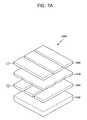
- FIG. 7Ais a schematic exploded view of a passive matrix type organic light emitting display device in accordance with one embodiment.
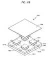
- FIG. 7Bis a schematic exploded view of an active matrix type organic light emitting display device in accordance with one embodiment.
- FIG. 7Cis a schematic top plan view of an organic light emitting display in accordance with one embodiment.
- FIG. 7Dis a cross-sectional view of the organic light emitting display of FIG. 7C , taken along the line d-d.
- FIG. 7Eis a schematic perspective view illustrating mass production of organic light emitting devices in accordance with one embodiment.
- OLEDorganic light emitting display
- OLEDis a display device comprising an array of organic light emitting diodes.
- Organic light emitting diodesare solid state devices which include an organic material and are adapted to generate and emit light when appropriate electrical potentials are applied.
- FIG. 7Aschematically illustrates an exploded view of a simplified structure of a passive matrix type OLED 1000 .
- FIG. 7Bschematically illustrates a simplified structure of an active matrix type OLED 1001 .
- the OLED 1000 , 1001includes OLED pixels built over a substrate 1002 , and the OLED pixels include an anode 1004 , a cathode 1006 and an organic layer 1010 .
- an appropriate electrical currentis applied to the anode 1004 , electric current flows through the pixels and visible light is emitted from the organic layer.
- the passive matrix OLED (PMOLED) designincludes elongate strips of anode 1004 arranged generally perpendicular to elongate strips of cathode 1006 with organic layers interposed therebetween.
- the intersections of the strips of cathode 1006 and anode 1004define individual OLED pixels where light is generated and emitted upon appropriate excitation of the corresponding strips of anode 1004 and cathode 1006 .
- PMOLEDsprovide the advantage of relatively simple fabrication.
- the active matrix OLEDincludes driving circuits 1012 arranged between the substrate 1002 and an array of OLED pixels.
- An individual pixel of AMOLEDsis defined between the common cathode 1006 and an anode 1004 , which is electrically isolated from other anodes.
- Each driving circuit 1012is coupled with an anode 1004 of the OLED pixels and further coupled with a data line 1016 and a scan line 1018 .
- the scan lines 1018supply select signals that select rows of the driving circuits
- the data lines 1016supply data signals for particular driving circuits.
- the data signals and scan signalsstimulate the local driving circuits 1012 , which excite the anodes 1004 so as to emit light from their corresponding pixels.
- the local driving circuits 1012 , the data lines 1016 and scan lines 1018are buried in a planarization layer 1014 , which is interposed between the pixel array and the substrate 1002 .
- the planarization layer 1014provides a planar top surface on which the organic light emitting pixel array is formed.
- the planarization layer 1014may be formed of organic or inorganic materials, and formed of two or more layers although shown as a single layer.
- the local driving circuits 1012are typically formed with thin film transistors (TFT) and arranged in a grid or array under the OLED pixel array.
- the local driving circuits 1012may be at least partly made of organic materials, including organic TFT.
- AMOLEDshave the advantage of fast response time improving their desirability for use in displaying data signals. Also, AMOLEDs have the advantages of consuming less power than passive matrix OLEDs.
- the substrate 1002provides structural support for the OLED pixels and circuits.
- the substrate 1002can comprise rigid or flexible materials as well as opaque or transparent materials, such as plastic, glass, and/or foil.
- each OLED pixel or diodeis formed with the anode 1004 , cathode 1006 and organic layer 1010 interposed therebetween.
- the cathode 1006injects electrons and the anode 1004 injects holes.
- the anode 1004 and cathode 1006are inverted; i.e., the cathode is formed on the substrate 1002 and the anode is opposingly arranged.
- Interposed between the cathode 1006 and anode 1004are one or more organic layers. More specifically, at least one emissive or light emitting layer is interposed between the cathode 1006 and anode 1004 .
- the light emitting layermay comprise one or more light emitting organic compounds. Typically, the light emitting layer is configured to emit visible light in a single color such as blue, green, red or white.
- one organic layer 1010is formed between the cathode 1006 and anode 1004 and acts as a light emitting layer.
- Additional layers, which can be formed between the anode 1004 and cathode 1006can include a hole transporting layer, a hole injection layer, an electron transporting layer and an electron injection layer.
- Hole transporting and/or injection layerscan be interposed between the light emitting layer 1010 and the anode 1004 . Electron transporting and/or injecting layers can be interposed between the cathode 1006 and the light emitting layer 1010 .
- the electron injection layerfacilitates injection of electrons from the cathode 1006 toward the light emitting layer 1010 by reducing the work function for injecting electrons from the cathode 1006 .
- the hole injection layerfacilitates injection of holes from the anode 1004 toward the light emitting layer 1010 .
- the hole and electron transporting layersfacilitate movement of the carriers injected from the respective electrodes toward the light emitting layer.
- a single layermay serve both electron injection and transportation functions or both hole injection and transportation functions. In some embodiments, one or more of these layers are lacking. In some embodiments, one or more organic layers are doped with one or more materials that help injection and/or transportation of the carriers. In embodiments where only one organic layer is formed between the cathode and anode, the organic layer may include not only an organic light emitting compound but also certain functional materials that help injection or transportation of carriers within that layer.
- organic materialsthat have been developed for use in these layers including the light emitting layer. Also, numerous other organic materials for use in these layers are being developed. In some embodiments, these organic materials may be macromolecules including oligomers and polymers. In some embodiments, the organic materials for these layers may be relatively small molecules. The skilled artisan will be able to select appropriate materials for each of these layers in view of the desired functions of the individual layers and the materials for the neighboring layers in particular designs.
- an electrical circuitprovides appropriate potential between the cathode 1006 and anode 1004 . This results in an electrical current flowing from the anode 1004 to the cathode 1006 via the interposed organic layer(s).
- the cathode 1006provides electrons to the adjacent organic layer 1010 .
- the anode 1004injects holes to the organic layer 1010 .
- the holes and electronsrecombine in the organic layer 1010 and generate energy particles called “excitons.”
- the excitonstransfer their energy to the organic light emitting material in the organic layer 1010 , and the energy is used to emit visible light from the organic light emitting material.
- the spectral characteristics of light generated and emitted by the OLED 1000 , 1001depend on the nature and composition of organic molecules in the organic layer(s).
- the composition of the one or more organic layerscan be selected to suit the needs of a particular application by one of ordinary skill in the art.
- OLED devicescan also be categorized based on the direction of the light emission.
- top emission typeOLED devices emit light and display images through the cathode or top electrode 1006 .
- the cathode 1006is made of a material transparent or at least partially transparent with respect to visible light.
- the anodemay be made of a material substantially reflective of the visible light.
- a second type of OLED devicesemits light through the anode or bottom electrode 1004 and is called “bottom emission” type.
- the anode 1004is made of a material which is at least partially transparent with respect to visible light.
- the cathode 1006is made of a material substantially reflective of the visible light.
- a third type of OLED devicesemits light in two directions, e.g. through both anode 1004 and cathode 1006 .
- the substratemay be formed of a material which is transparent, opaque or reflective of visible light.
- an OLED pixel array 1021comprising a plurality of organic light emitting pixels is arranged over a substrate 1002 as shown in FIG. 7C .
- the pixels in the array 1021are controlled to be turned on and off by a driving circuit (not shown), and the plurality of the pixels as a whole displays information or image on the array 1021 .
- the OLED pixel array 1021is arranged with respect to other components, such as drive and control electronics to define a display region and a non-display region.
- the display regionrefers to the area of the substrate 1002 where OLED pixel array 1021 is formed.
- the non-display regionrefers to the remaining areas of the substrate 1002 .
- the non-display regioncan contain logic and/or power supply circuitry. It will be understood that there will be at least portions of control/drive circuit elements arranged within the display region. For example, in PMOLEDs, conductive components will extend into the display region to provide appropriate potential to the anode and cathodes. In AMOLEDs, local driving circuits and data/scan lines coupled with the driving circuits will extend into the display region to drive and control the individual pixels of the AMOLEDs.
- FIG. 7Dschematically illustrates a cross-section of an encapsulated OLED device 1011 having a layout of FIG. 7C and taken along the line d-d of FIG. 7C .
- a generally planar top plate or substrate 1061engages with a seal 1071 which further engages with a bottom plate or substrate 1002 to enclose or encapsulate the OLED pixel array 1021 .
- one or more layersare formed on the top plate 1061 or bottom plate 1002 , and the seal 1071 is coupled with the bottom or top substrate 1002 , 1061 via such a layer.
- the seal 1071extends along the periphery of the OLED pixel array 1021 or the bottom or top plate 1002 , 1061 .
- the seal 1071is made of a frit material as will be further discussed below.
- the top and bottom plates 1061 , 1002comprise materials such as plastics, glass and/or metal foils which can provide a barrier to passage of oxygen and/or water to thereby protect the OLED pixel array 1021 from exposure to these substances.
- at least one of the top plate 1061 and the bottom plate 1002are formed of a substantially transparent material.
- seal 1071 and the top and bottom plates 1061 , 1002provide a substantially non-permeable seal to oxygen and water vapor and provide a substantially hermetically enclosed space 1081 .
- the seal 1071 of a frit material in combination with the top and bottom plates 1061 , 1002provide a barrier to oxygen of less than approximately 10 ⁇ 3 cc/m 2 -day and to water of less than 10 ⁇ 6 g/m 2 -day.
- a material that can take up oxygen and/or moistureis formed within the enclosed space 1081 .
- the seal 1071has a width W, which is its thickness in a direction parallel to a surface of the top or bottom substrate 1061 , 1002 as shown in FIG. 7D .
- the widthvaries among embodiments and ranges from about 300 ⁇ m to about 3000 ⁇ m, optionally from about 500 ⁇ m to about 1500 ⁇ m. Also, the width may vary at different positions of the seal 1071 . In some embodiments, the width of the seal 1071 may be the largest where the seal 1071 contacts one of the bottom and top substrate 1002 , 1061 or a layer formed thereon. The width may be the smallest where the seal 1071 contacts the other.
- the width variation in a single cross-section of the seal 1071relates to the cross-sectional shape of the seal 1071 and other design parameters.
- the seal 1071has a height H, which is its thickness in a direction perpendicular to a surface of the top or bottom substrate 1061 , 1002 as shown in FIG. 7D .
- the heightvaries among embodiments and ranges from about 2 ⁇ m to about 30 ⁇ m, optionally from about 10 ⁇ m to about 15 ⁇ m. Generally, the height does not significantly vary at different positions of the seal 1071 . However, in certain embodiments, the height of the seal 1071 may vary at different positions thereof.
- the seal 1071has a generally rectangular cross-section. In other embodiments, however, the seal 1071 can have other various cross-sectional shapes such as a generally square cross-section, a generally trapezoidal cross-section, a cross-section with one or more rounded edges, or other configuration as indicated by the needs of a given application. To improve hermeticity, it is generally desired to increase the interfacial area where the seal 1071 directly contacts the bottom or top substrate 1002 , 1061 or a layer formed thereon. In some embodiments, the shape of the seal can be designed such that the interfacial area can be increased.
- the seal 1071can be arranged immediately adjacent the OLED array 1021 , and in other embodiments, the seal 1071 is spaced some distance from the OLED array 1021 .
- the seal 1071comprises generally linear segments that are connected together to surround the OLED array 1021 . Such linear segments of the seal 1071 can extend, in certain embodiments, generally parallel to respective boundaries of the OLED array 1021 .
- one or more of the linear segments of the seal 1071are arranged in a non-parallel relationship with respective boundaries of the OLED array 1021 .
- at least part of the seal 1071extends between the top plate 1061 and bottom plate 1002 in a curvilinear manner.
- the seal 1071is formed using a frit material or simply “frit” or glass frit,” which includes fine glass particles.
- the frit particlesincludes one or more of magnesium oxide (MgO), calcium oxide (CaO), barium oxide (BaO), lithium oxide (Li 2 O), sodium oxide (Na 2 O), potassium oxide (K 2 O), boron oxide (B 2 O 3 ), vanadium oxide (V 2 O 5 ), zinc oxide (ZnO), tellurium oxide (TeO 2 ), aluminum oxide (Al 2 O 3 ), silicon dioxide (SiO 2 ), lead oxide (PbO), tin oxide (SnO), phosphorous oxide (P 2 O 5 ), ruthenium oxide (Ru 2 O), rubidium oxide (Rb 2 O), rhodium oxide (Rh 2 O), ferrite oxide (Fe 2 O 3 ), copper oxide (CuO), titanium oxide (TiO 2 ), tungsten oxide (WO 3 ), bismuth oxide (Bi 2
- these particlesrange in size from about 2 ⁇ m to about 30 ⁇ m, optionally about 5 ⁇ m to about 10 ⁇ m, although not limited only thereto.
- the particlescan be as large as about the distance between the top and bottom substrates 1061 , 1002 or any layers formed on these substrates where the frit seal 1071 contacts.
- the frit material used to form the seal 1071can also include one or more filler or additive materials.
- the filler or additive materialscan be provided to adjust an overall thermal expansion characteristic of the seal 1071 and/or to adjust the absorption characteristics of the seal 1071 for selected frequencies of incident radiant energy.
- the filler or additive material(s)can also include inversion and/or additive fillers to adjust a coefficient of thermal expansion of the frit.
- the filler or additive materialscan include transition metals, such as chromium (Cr), iron (Fe), manganese (Mn), cobalt (Co), copper (Cu), and/or vanadium. Additional materials for the filler or additives include ZnSiO 4 , PbTiO 3 , ZrO 2 , eucryptite.
- a frit material as a dry compositioncontains glass particles from about 20 to 90 about wt %, and the remaining includes fillers and/or additives.
- the frit pastecontains about 10-30 wt % organic materials and about 70-90% inorganic materials.
- the frit pastecontains about 20 wt % organic materials and about 80 wt % inorganic materials.
- the organic materialsmay include about 0-30 wt % binder(s) and about 70-100 wt % solvent(s).
- about 10 wt %is binder(s) and about 90 wt % is solvent(s) among the organic materials.
- the inorganic materialsmay include about 0-10 wt % additives, about 20-40 wt % fillers and about 50-80 wt % glass powder. In some embodiments, about 0-5 wt % is additive(s), about 25-30 wt % is filler(s) and about 65-75 wt % is the glass powder among the inorganic materials.
- a liquid materialis added to the dry frit material to form a frit paste.
- Any organic or inorganic solvent with or without additivescan be used as the liquid material.
- the solventincludes one or more organic compounds.
- applicable organic compoundsare ethyl cellulose, nitro cellulose, hydroxyl propyl cellulose, butyl carbitol acetate, terpineol, butyl cellusolve, acrylate compounds.
- a shape of the seal 1071is initially formed from the frit paste and interposed between the top plate 1061 and the bottom plate 1002 .
- the seal 1071can in certain embodiments be pre-cured or pre-sintered to one of the top plate and bottom plate 1061 , 1002 .
- portions of the seal 1071are selectively heated such that the frit material forming the seal 1071 at least partially melts.
- the seal 1071is then allowed to resolidify to form a secure joint between the top plate 1061 and the bottom plate 1002 to thereby inhibit exposure of the enclosed OLED pixel array 1021 to oxygen or water.
- the selective heating of the frit sealis carried out by irradiation of light, such as a laser or directed infrared lamp.
- the frit material forming the seal 1071can be combined with one or more additives or filler such as species selected for improved absorption of the irradiated light to facilitate heating and melting of the frit material to form the seal 1071 .
- OLED devices 1011are mass produced.
- a plurality of separate OLED arrays 1021is formed on a common bottom substrate 1101 .
- each OLED array 1021is surrounded by a shaped frit to form the seal 1071 .
- common top substrate(not shown) is placed over the common bottom substrate 1101 and the structures formed thereon such that the OLED arrays 1021 and the shaped frit paste are interposed between the common bottom substrate 1101 and the common top substrate.
- the OLED arrays 1021are encapsulated and sealed, such as via the previously described enclosure process for a single OLED display device.
- the resulting productincludes a plurality of OLED devices kept together by the common bottom and top substrates.
- the resulting productis cut into a plurality of pieces, each of which constitutes an OLED device 1011 of FIG. 7D .
- the individual OLED devices 1011then further undergo additional packaging operations to further improve the sealing formed by the frit seal 1071 and the top and bottom substrates 1061 , 1002 .
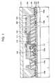
- FIG. 1is a cross-sectional view of an organic light emitting display according to an embodiment.
- the organic light emitting displayincludes a semiconductor layer 110 , a gate insulating layer 120 , a gate electrode 130 a , a scan driver 130 b , an interlayer insulating layer 140 , and source and drain electrodes 150 , which are disposed on a substrate 100 having a pixel region I and a non-pixel region II.
- the organic light emitting displayfurther includes a common power supply line 150 b , and a second electrode power supply line 150 a , which are formed of source and drain interconnections.
- a planarization layer 160is disposed on the entire surface of the substrate 100 .
- the planarization layer 160is formed of an organic material such as acryl-based resin or polyimide-based resin.
- the planarization layer 160has via-holes for exposing the common power supply line 150 b , the second electrode power supply line 150 a , and the source and/or drain electrodes 150 .
- the common power supply line 150 bis partially exposed to enhance adhesive strength when the substrate is sealed using a glass frit.
- a first electrode 171 including a reflective layer 170is disposed on the substrate 100 , and a pixel defining layer 180 is disposed on the entire surface of the substrate 100 .
- An organic layer 190 including at least an emission layeris disposed on the first electrode 171 , and a second electrode 200 is disposed thereon.
- An encapsulation substrate 210is disposed opposite to the substrate 100 , and the substrate 100 and the encapsulation substrate 210 are sealed with a glass frit 220 , thereby forming an organic light emitting display.
- the organic light emitting displayincludes an organic planarization layer disposed under the glass frit for sealing the substrate so that the organic planarization layer may be damaged due to a large amount of heat generated when a laser beam is radiated to the glass frit. As a result, adhesive strength at an interface in which the glass frit is adhered to the organic planarization layer may be lowered.
- FIGS. 2 to 5are cross-sectional views of an organic light emitting display in accordance with another embodiment.
- a substrate 300 including a pixel region I, and a non-pixel region IIis provided.
- the substrate 300may be an insulating glass substrate, a plastic substrate, or a conductive substrate.
- a buffer layer 310is formed on the surface of the substrate 300 .
- the buffer layer 310may be a silicon oxide layer, a silicon nitride layer, or a composite layer of silicon oxide and silicon nitride.
- the buffer layer 310functions as a passivation layer for preventing impurities from out-diffusing from the substrate 300 .
- a semiconductor layer 320is formed on the buffer layer 310 in the pixel region I.
- the semiconductor layer 320may be an amorphous silicon layer or a polysilicon layer.
- a gate insulating layer 330is formed on the surface of the substrate 300 and the semiconductor layer 320 .
- the gate insulating layer 330may be a silicon oxide layer, a silicon nitride layer, or a composite layer of silicon oxide and silicon nitride.
- a gate electrode 340 ais formed on the gate insulating layer 330 located above a portion of the semiconductor layer 320 .
- the gate electrode 340 amay be comprised of Al, Cu, and/or Cr.
- the interlayer insulating layer 350is formed on the surface of the substrate 300 and the gate electrode 340 a .
- the interlayer insulating layer 350may be a silicon oxide layer, a silicon nitride layer, or a composite layer of silicon oxide and silicon nitride.
- Source and drain electrodes 360 a and 360 bare formed on the interlayer insulating layer 350 in the pixel region I connecting to the semiconductor layer 320 through the contact holes 351 and 352 .
- the source and drain electrodes 360 a and 360 bmay be formed of one or more materials including, for example, Mo, Cr, Al, Ti, Au, Pd and Ag.
- the electrically conductive line 360 dis formed in the non-pixel region II.
- the electrically conductive line 360 dmay act as a common power supply line.
- a second electrode power supply line 360 cmay also be formed at the same time.
- a scan driver line 340 bmay be formed in the non-pixel region II.
- a bottom gate thin film transistor having a gate electrode disposed under a semiconductor layermay also be formed.
- the electrically conductive linein this embodiment, is formed at the same time the source and drain electrodes are formed, the electrically conductive line may also be formed at the same time the gate electrode or the first electrode is formed.
- an organic planarization layer 370is formed on the surface of the substrate 300 .
- the organic planarization layer 370may be formed using an organic material such as acryl-based resin, polyimide-based resin, or benzocyclobutene (BCB).
- the organic planarization layer 370is then etched to form via-holes 371 a and 371 b for exposing at least one of the source and/or drain electrodes 360 a and 360 b in the pixel region I, and the second electrode power supply line 360 c in the non-pixel region II.
- the organic planarization layer 370 in the non-pixel region II, where the electrically conductive line 360 d is locatedis removed by etching to form a recess exposing the electrically conductive line 360 d .
- the glass fritis irradiated with a laser beam to adhere the substrates.
- the organic planarization layermay be damaged due to a large amount of heat generated from the laser.
- the glass fritmay be delaminated from an interface with the planarization layer to decrease adhesive strength thereof. Therefore, the organic planarization layer at the edge of the substrate 300 , to which the glass frit is to be adhered, is removed to prevent the above problems.
- a first electrode 380 including a reflective layer 375is formed on the organic planarization layer 370 in the pixel region I.
- the first electrode 380is disposed on a bottom surface of the via-hole 371 to be in contact with one of the exposed source and/or drain electrodes 360 a and 360 b , and extends onto the organic planarization layer 370 .
- the first electrode 380may be formed of indium tin oxide (ITO) or indium zinc oxide (IZO).
- a pixel defining layer 390is formed on the surface of the substrate 300 including at least the first electrode 380 .
- the pixel defining layeris formed to a thickness sufficient to fill the via-hole 371 a , in which the first electrode 380 is disposed.
- the pixel defining layer 390may be formed of an organic layer or an inorganic layer, preferably, an organic layer. More preferably, the pixel defining layer 390 is formed of one selected from the group including BCB, acryl-based polymer, and polyimide.
- the material comprising the pixel defining layer 390preferably has high flowability such that the pixel defining layer can be evenly formed on the entire surface of the substrate.
- the pixel defining layer 390is etched to form openings 395 a for exposing the first electrode 380 in the pixel region I, and a portion of the second electrode power supply line 360 c in the non-pixel region II.
- the pixel defining layer 390 in the non-pixel region II, at which the electrically conductive line 360 d is disposed,is also removed by etching.
- an organic layer 400is formed on the first electrode 380 exposed through the opening 395 a .
- the organic layer 400includes at least an emission layer, and may further include at least one of a hole injection layer, a hole transport layer, an electron transport layer, and an electron injection layer.
- the second electrode 410is a transmissive electrode, and may be formed of Mg, Ag, Al, Ca, or an alloy thereof, which is transparent and has a low work function. At this time, the second electrode 410 is etched to expose the electrically conductive line 360 d in the non-pixel region II.
- an encapsulation substrate 420 opposite to the substrate 300is provided.
- the encapsulation substrate 420may be formed of an etched insulating glass or a non-etched insulating glass.
- a glass frit 430is applied to the edge of the encapsulation substrate 420 opposite to the substrate 300 .
- the glass frit 430may be formed of material selected from the group consisting of magnesium oxide (MgO), calcium oxide (CaO), barium oxide (BaO), lithium oxide (Li 2 O), sodium oxide (Na 2 O), potassium oxide (K 2 O), boron oxide (B 2 ) 3 ), vanadium oxide (V 2 O 5 ), zinc oxide (ZnO), tellurium oxide (TeO 2 ), aluminum oxide (Al 2 O 3 ), silicon dioxide (SiO 2 ), lead oxide (PbO), tin oxide (SnO), phosphorous oxide (P 2 O 5 ), ruthenium oxide (Ru 2 O), rubidium oxide (Rb 2 O), rhodium oxide (Rh 2 O), ferrite oxide (Fe 2 O 3 ), copper oxide (CuO), titanium oxide (TiO 2 ), tungsten oxide (WO 3 ), bismuth oxide (M
- the glass frit 430has a width larger than that of the electrically conductive line 360 d . As the glass frit 430 has a larger width, the adhesive strength increases. Therefore, it is possible to protect an element from external moisture or oxygen.
- the glass frit 430is applied on the encapsulating substrate 420 . In other embodiments, the glass frit 430 may be applied on the substrate 300 , or on both the substrate 300 and the encapsulation substrate 420 .
- the substrate 300 and the encapsulation substrate 420are aligned and adhered to each other. At this time, the glass frit 430 is in contact with the electrically conductive line 360 d and the interlayer insulating layer 350 on the substrate 300 .
- the glass frit 430After contacting the substrate 300 with the encapsulation substrate 420 via the glass frit 430 , the glass frit 430 is irradiated with a laser beam. The glass frit 430 is melted and solidified to adhere the substrate 300 and the encapsulation substrate 420 , thereby completing the organic light emitting display of an embodiment.
- multiple arrays of organic light emitting pixelsmay be encapsulated between a single substrate 300 and a single encapsulation substrate 420 and be surrounded by additional glass frits 430 (e.g., in a mass production configuration). The multiple arrays may be cut apart resulting in individual arrays encapsulated by the substrate 300 , the encapsulation substrate 420 and a glass frit 430 .
- the organic planarization layermay be damaged due to the large amount of heat generated when the laser beam is radiated to the glass frit. As a result, the glass frit may be delaminated from an interface with the planarization layer to decrease adhesive strength thereof. On the other hand, the organic planarization layer in the area of the glass frit may be removed to prevent adhesive strength of the glass frit from being lowered.
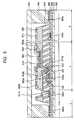
- FIG. 6is a cross-sectional view of an organic light emitting display in accordance with another embodiment of the present invention.
- the organic light emitting displayis formed in a manner similar to the embodiment discussed above in reference to FIGS. 2-5 , where a glass frit 630 is applied on an encapsulating substrate 620 , and a substrate 500 is adhered to the encapsulating substrate 620 .
- the glass frit 630is then irradiated with a laser beam such that the glass frit 630 is melted and solidified, thereby completing the organic light emitting display.
- the glass frit 630has a width equal to or smaller than that of the electrically conductive line 560 d .
- the glass frit 430was wider than the electrically conductive line 560 d .
- the electrically conductive line 560 dsubstantially eclipses or totally eclipses the glass frit 630 as viewed from the substrate 300 .
- the wider glass frit 430may provide increased adhesive strength compared to the glass frit 630
- a narrower glass fritsuch as the glass frit 630 may be sufficient, depending on the embodiment.
- an organic planarization layerdoes not exist under the glass frit (either the glass frit 430 or the glass frit 630 ), it is possible to prevent the adhesive strength of either of the glass frits 430 or 630 from being lowered.
- the glass frit 630is applied on the encapsulating substrate 620 .
- the glass frit 430may be applied on the substrate 500 , or on both the substrate 500 and the encapsulating substrate 620 .
- the organic planarization layeris disposed under the glass frit for sealing the substrate so that the organic planarization layer may be damaged due to the large amount of heat generated when the laser beam is radiated to the glass frit.
- the glass fritmay be delaminated from an interface with the planarization layer to decrease adhesive strength thereof.
- the organic planarization layer under the glass fritis removed to prevent adhesive strength of the glass frit from being lowered. Therefore, it is possible to prevent intrusion of external moisture or oxygen to improve reliability of an element.
- the electrically conductive linemay be disposed on and under the substrate and under the glass frit.
- an organic light emitting display and a method of fabricating the same in accordance with the present inventioncan prevent adhesive strength of a glass frit from being lowered when a substrate is sealed using the glass frit, thereby improving reliability.
Landscapes
- Engineering & Computer Science (AREA)
- Microelectronics & Electronic Packaging (AREA)
- Physics & Mathematics (AREA)
- Optics & Photonics (AREA)
- Electroluminescent Light Sources (AREA)
- Devices For Indicating Variable Information By Combining Individual Elements (AREA)
Abstract
Description
| Application | ||
| Title | Filing Date | No. |
| ORGANIC LIGHT-EMITTING DISPLAY | Sep. 29, 2006 | 11/541,055 |
| DEVICE AND METHOD OF | ||
| FABRICATING THE SAME | ||
| ORGANIC LIGHT-EMITTING DISPLAY | Sep. 29, 2006 | 11/529,914 |
| DEVICE AND METHOD OF | ||
| MANUFACTURING THE SAME | ||
| ORGANIC LIGHT EMITTING DISPLAY | Sep. 29, 2006 | 11/541,139 |
| DEVICE | ||
| ORGANIC LIGHT-EMITTING DISPLAY | Sep. 29, 2006 | 11/541,047 |
| DEVICE WITH FRIT SEAL AND | ||
| REINFORCING STRUCTURE | ||
| ORGANIC LIGHT EMITTING DISPLAY | Sep. 29, 2006 | 11/540,150 |
| DEVICE METHOD OF FABRICATING | ||
| THE SAME | ||
| ORGANIC LIGHT EMITTING DISPLAY | Sep. 29, 2006 | 11/541,009 |
| AND METHOD OF FABRICATING THE | ||
| SAME | ||
| ORGANIC LIGHT-EMITTING DISPLAY | Sep. 29, 2006 | 11/540,151 |
| DEVICE WITH FRIT SEAL AND | ||
| REINFORCING STRUCTURE BONDED | ||
| TO FRAME | ||
| METHOD FOR PACKAGING ORGANIC | Sep. 29, 2006 | 11/529,910 |
| LIGHT EMITTING DISPLAY WITH | ||
| FRIT SEAL AND REINFORCING | ||
| STRUCTURE | ||
| METHOD FOR PACKAGING ORGANIC | Sep. 29, 2006 | 11/540,084 |
| LIGHT EMITTING DISPLAY WITH | ||
| FRIT SEAL AND REINFORCING | ||
| STRUCTURE | ||
| ORGANIC LIGHT-EMITTING DISPLAY | Sep. 29, 2006 | 11/540,008 |
| DEVICE AND THE PREPARATION | ||
| METHOD OF THE SAME | ||
| ORGANIC LIGHT EMITTING DISPLAY | Sep. 29, 2006 | 11/541,048 |
| AND FABRICATING METHOD OF THE | ||
| SAME | ||
| ORGANIC LIGHT-EMITTING DISPLAY | Sep. 29, 2006 | 11/540,021 |
| AND METHOD OF MAKING THE | ||
| SAME | ||
| ORGANIC LIGHT EMITTING DISPLAY | Sep. 29, 2006 | 11/540,024 |
| AND FABRICATING METHOD OF THE | ||
| SAME | ||
| ORGANIC LIGHT EMITTING DISPLAY | Sep. 29, 2006 | 11/529,995 |
| DEVICE AND MANUFACTURING | ||
| METHOD THEREOF | ||
| ORGANIC LIGHT-EMITTING DISPLAY | Sep. 29, 2006 | 11/540,157 |
| DEVICE AND MANUFACTURING | ||
| METHOD OF THE SAME | ||
| ORGANIC LIGHT EMITTING DISPLAY | Sep. 29, 2006 | 11/540,149 |
| AND FABRICATING METHOD OF THE | ||
| SAME | ||
| ORGANIC LIGHT EMITTING DISPLAY | Sep. 29, 2006 | 11/529,916 |
| AND METHOD OF FABRICATING THE | ||
| SAME | ||
| ORGANIC LIGHT EMITTING DISPLAY | Sep. 29, 2006 | 11/529,891 |
| DEVICE METHOD OF FABRICATING | ||
| THE SAME | ||
Claims (24)
Applications Claiming Priority (4)
| Application Number | Priority Date | Filing Date | Title |
|---|---|---|---|
| KR10-2006-0007962 | 2006-01-25 | ||
| KR20060007962 | 2006-01-25 | ||
| KR10-2006-0027321 | 2006-03-27 | ||
| KR1020060027321AKR100712185B1 (en) | 2006-01-25 | 2006-03-27 | Organic light emitting display device and manufacturing method |
Publications (2)
| Publication Number | Publication Date |
|---|---|
| US20070170859A1 US20070170859A1 (en) | 2007-07-26 |
| US8164257B2true US8164257B2 (en) | 2012-04-24 |
Family
ID=38284877
Family Applications (1)
| Application Number | Title | Priority Date | Filing Date |
|---|---|---|---|
| US11/540,103Active2028-11-03US8164257B2 (en) | 2006-01-25 | 2006-09-29 | Organic light emitting display and method of fabricating the same |
Country Status (2)
| Country | Link |
|---|---|
| US (1) | US8164257B2 (en) |
| JP (1) | JP2007200887A (en) |
Cited By (23)
| Publication number | Priority date | Publication date | Assignee | Title |
|---|---|---|---|---|
| US8623469B2 (en) | 2011-10-21 | 2014-01-07 | Semiconductor Energy Laboratory Co., Ltd. | Method of heating dispersion composition and method of forming glass pattern |
| US8816336B2 (en) | 2011-06-16 | 2014-08-26 | Semiconductor Energy Laboratory Co., Ltd. | Sealed body, method for manufacturing sealed body, light-emitting device, and method for manufacturing light-emitting device |
| US8950216B2 (en) | 2011-05-13 | 2015-02-10 | Semiconductor Energy Laboratory Co., Ltd. | Method for manufacturing glass sealed body and method for manufacturing light-emitting device |
| US9004972B2 (en) | 2006-01-20 | 2015-04-14 | Samsung Display Co., Ltd. | Organic light-emitting display device with frit seal and reinforcing structure |
| US9048350B2 (en) | 2011-11-28 | 2015-06-02 | Semiconductor Energy Laboratory Co., Ltd. | Sealed body, light-emitting module and method of manufacturing sealed body |
| US9214643B2 (en) | 2011-11-29 | 2015-12-15 | Semiconductor Energy Laboratory Co., Ltd. | Sealed structure, light-emitting device, electronic device, and lighting device |
| US9216557B2 (en) | 2011-11-29 | 2015-12-22 | Semiconductor Energy Laboratory Co., Ltd. | Sealed structure, light-emitting device, electronic device, and lighting device |
| US9258853B2 (en) | 2011-08-26 | 2016-02-09 | Semiconductor Energy Laboratory Co., Ltd. | Light-emitting device, electronic device, lighting device, and method for manufacturing the light-emitting device |
| US20160079324A1 (en)* | 2014-09-16 | 2016-03-17 | Samsung Display Co., Ltd. | Display apparatus |
| US9299943B2 (en) | 2011-11-28 | 2016-03-29 | Semiconductor Energy Laboratory Co., Ltd. | Glass pattern and method for forming the same, sealed body and method for manufacturing the same, and light-emitting device |
| US9362522B2 (en) | 2012-10-26 | 2016-06-07 | Semiconductor Energy Laboratory Co., Ltd. | Method for bonding substrates, method for manufacturing sealing structure, and method for manufacturing light-emitting device |
| US9440880B2 (en) | 2011-06-17 | 2016-09-13 | Semiconductor Energy Laboratory Co., Ltd. | Method of manufacturing light-emitting device |
| US9472776B2 (en) | 2011-10-14 | 2016-10-18 | Semiconductor Energy Laboratory Co., Ltd. | Method for manufacturing sealed structure including welded glass frits |
| US9502683B2 (en) | 2014-06-24 | 2016-11-22 | Samsung Display Co., Ltd. | Sealing portion structure for display device |
| US20170098797A1 (en)* | 2015-10-06 | 2017-04-06 | Samsung Display Co., Ltd. | Display apparatus |
| US9633871B2 (en) | 2011-08-24 | 2017-04-25 | Semiconductor Energy Laboratory Co., Ltd. | Light-emitting device |
| US9666755B2 (en) | 2011-11-29 | 2017-05-30 | Semiconductor Energy Laboratory Co., Ltd. | Method of manufacturing sealed body and method of manufacturing light-emitting device |
| US9853242B2 (en) | 2012-07-30 | 2017-12-26 | Semiconductor Energy Laboratory Co., Ltd. | Sealing structure and organic electroluminescence device |
| US10068926B2 (en) | 2011-05-05 | 2018-09-04 | Semiconductor Energy Laboratory Co., Ltd. | Semiconductor device and method for manufacturing the same |
| US10083992B2 (en) | 2014-09-23 | 2018-09-25 | Samsung Display Co., Ltd. | Display device |
| US10319800B2 (en)* | 2016-06-20 | 2019-06-11 | Wuhan China Star Optoelectronics Technology Co., Ltd | OLED display screen |
| US10916598B2 (en)* | 2018-06-15 | 2021-02-09 | Hefei Xinsheng Optoelectronics Technology Co., Ltd. | OLED array substrate, method for fabricating the same, OLED pixel circuit, and display device |
| US10937840B2 (en)* | 2018-06-28 | 2021-03-02 | Samsung Display Co., Ltd. | Display device |
Families Citing this family (55)
| Publication number | Priority date | Publication date | Assignee | Title |
|---|---|---|---|---|
| KR100645533B1 (en)* | 2005-05-27 | 2006-11-14 | 삼성에스디아이 주식회사 | Organic light emitting display device and manufacturing method thereof |
| US20070108900A1 (en)* | 2005-11-15 | 2007-05-17 | Boek Heather D | Method and apparatus for the elimination of interference fringes in an OLED device |
| US7425166B2 (en)* | 2005-12-06 | 2008-09-16 | Corning Incorporated | Method of sealing glass substrates |
| US7597603B2 (en)* | 2005-12-06 | 2009-10-06 | Corning Incorporated | Method of encapsulating a display element |
| US7537504B2 (en)* | 2005-12-06 | 2009-05-26 | Corning Incorporated | Method of encapsulating a display element with frit wall and laser beam |
| US8038495B2 (en) | 2006-01-20 | 2011-10-18 | Samsung Mobile Display Co., Ltd. | Organic light-emitting display device and manufacturing method of the same |
| KR100635514B1 (en) | 2006-01-23 | 2006-10-18 | 삼성에스디아이 주식회사 | Organic light emitting display device and manufacturing method |
| JP4456092B2 (en)* | 2006-01-24 | 2010-04-28 | 三星モバイルディスプレイ株式會社 | Organic electroluminescent display device and manufacturing method thereof |
| JP4624309B2 (en)* | 2006-01-24 | 2011-02-02 | 三星モバイルディスプレイ株式會社 | Organic electroluminescent display device and manufacturing method thereof |
| KR100671641B1 (en) | 2006-01-25 | 2007-01-19 | 삼성에스디아이 주식회사 | Organic electroluminescent display and manufacturing method thereof |
| KR100688796B1 (en)* | 2006-01-25 | 2007-03-02 | 삼성에스디아이 주식회사 | Organic light emitting display device and manufacturing method thereof |
| KR100688795B1 (en)* | 2006-01-25 | 2007-03-02 | 삼성에스디아이 주식회사 | Organic light emitting display device and manufacturing method |
| KR100685853B1 (en)* | 2006-01-25 | 2007-02-22 | 삼성에스디아이 주식회사 | Organic light emitting display device and manufacturing method |
| JP4633674B2 (en) | 2006-01-26 | 2011-02-16 | 三星モバイルディスプレイ株式會社 | Organic electroluminescent display device and manufacturing method thereof |
| KR100732808B1 (en)* | 2006-01-26 | 2007-06-27 | 삼성에스디아이 주식회사 | Manufacturing method of organic light emitting display device |
| KR100671647B1 (en)* | 2006-01-26 | 2007-01-19 | 삼성에스디아이 주식회사 | Organic light emitting display device |
| KR100688790B1 (en)* | 2006-01-27 | 2007-03-02 | 삼성에스디아이 주식회사 | Organic electroluminescent display and manufacturing method thereof |
| KR100671639B1 (en)* | 2006-01-27 | 2007-01-19 | 삼성에스디아이 주식회사 | Organic electroluminescent display and manufacturing method thereof |
| KR100688792B1 (en)* | 2006-01-27 | 2007-03-02 | 삼성에스디아이 주식회사 | Flat panel display and manufacturing method thereof |
| KR100759666B1 (en)* | 2006-01-27 | 2007-09-17 | 삼성에스디아이 주식회사 | Flat panel display and manufacturing method thereof |
| US20070188757A1 (en)* | 2006-02-14 | 2007-08-16 | Jeffrey Michael Amsden | Method of sealing a glass envelope |
| KR100732817B1 (en) | 2006-03-29 | 2007-06-27 | 삼성에스디아이 주식회사 | Organic light emitting display device and manufacturing method |
| US20070267972A1 (en)* | 2006-05-22 | 2007-11-22 | Menegus Harry E | Method for forming a temporary hermetic seal for an OLED display device |
| US20080124558A1 (en)* | 2006-08-18 | 2008-05-29 | Heather Debra Boek | Boro-silicate glass frits for hermetic sealing of light emitting device displays |
| US20080048556A1 (en)* | 2006-08-24 | 2008-02-28 | Stephan Lvovich Logunov | Method for hermetically sealing an OLED display |
| US20080049431A1 (en)* | 2006-08-24 | 2008-02-28 | Heather Debra Boek | Light emitting device including anti-reflection layer(s) |
| US7800303B2 (en)* | 2006-11-07 | 2010-09-21 | Corning Incorporated | Seal for light emitting display device, method, and apparatus |
| KR100841362B1 (en)* | 2006-11-10 | 2008-06-26 | 삼성에스디아이 주식회사 | Organic light emitting display device and manufacturing method thereof |
| US20080168801A1 (en)* | 2007-01-12 | 2008-07-17 | Paul Stephen Danielson | Method of sealing glass |
| US20080200088A1 (en)* | 2007-02-21 | 2008-08-21 | Chong Pyung An | Method for reducing interference fringes in a display device |
| US7652305B2 (en)* | 2007-02-23 | 2010-01-26 | Corning Incorporated | Methods and apparatus to improve frit-sealed glass package |
| US20080213482A1 (en)* | 2007-03-01 | 2008-09-04 | Stephan Lvovich Logunov | Method of making a mask for sealing a glass package |
| US20090044496A1 (en)* | 2007-08-16 | 2009-02-19 | Botelho John W | Method and apparatus for sealing a glass package |
| US20090058293A1 (en)* | 2007-08-31 | 2009-03-05 | Norihisa Maeda | Display device |
| JP5506172B2 (en)* | 2007-10-10 | 2014-05-28 | 株式会社半導体エネルギー研究所 | Method for manufacturing semiconductor substrate |
| US7936122B2 (en)* | 2007-12-14 | 2011-05-03 | Canon Kabushiki Kaisha | Organic EL display apparatus |
| US8448468B2 (en) | 2008-06-11 | 2013-05-28 | Corning Incorporated | Mask and method for sealing a glass envelope |
| KR100995071B1 (en) | 2008-09-12 | 2010-11-18 | 삼성모바일디스플레이주식회사 | Organic light emitting display |
| KR102029563B1 (en) | 2008-12-11 | 2019-10-07 | 오스람 오엘이디 게엠베하 | Organic light-emitting diode and luminaire |
| KR20110019498A (en)* | 2009-08-20 | 2011-02-28 | 삼성모바일디스플레이주식회사 | Organic light emitting display |
| KR101826069B1 (en)* | 2010-10-26 | 2018-03-23 | 삼성디스플레이 주식회사 | Organic light emitting display device and manufacturing method thereof |
| KR101818451B1 (en)* | 2010-12-24 | 2018-01-16 | 엘지디스플레이 주식회사 | Organic light emitting diode display device and method of fabricating the same |
| KR101782165B1 (en) | 2011-07-18 | 2017-09-27 | 엘지디스플레이 주식회사 | Organic electro-luminescence display and manufacturing method thereof |
| KR20130128940A (en)* | 2012-05-18 | 2013-11-27 | 삼성디스플레이 주식회사 | Organic light emitting display apparatus and the manufacturing method thereof |
| KR102090703B1 (en)* | 2013-05-21 | 2020-04-16 | 삼성디스플레이 주식회사 | Organinc light emitting display device and manufacturing method for the same |
| JP6133173B2 (en)* | 2013-08-29 | 2017-05-24 | 株式会社ジャパンディスプレイ | Organic electroluminescence display device |
| KR102283856B1 (en)* | 2013-11-22 | 2021-08-03 | 삼성디스플레이 주식회사 | Organic Light Emitting Display and Fabrication Method for the same |
| KR102210210B1 (en)* | 2014-01-06 | 2021-02-02 | 삼성디스플레이 주식회사 | Organic light emitting display apparatus |
| KR20160072406A (en)* | 2014-12-15 | 2016-06-23 | 엘지디스플레이 주식회사 | Organic light emitting diode display pannel |
| KR102568631B1 (en)* | 2016-04-15 | 2023-08-21 | 삼성디스플레이 주식회사 | Organic light emitting diode display device |
| CN105739154B (en)* | 2016-04-29 | 2019-09-27 | 上海天马有机发光显示技术有限公司 | A display panel and electronic device |
| CN107170900B (en) | 2017-05-12 | 2019-11-22 | 京东方科技集团股份有限公司 | OLED substrate and preparation method thereof, and display device |
| CN108336109B (en)* | 2018-01-02 | 2021-02-02 | 厦门天马微电子有限公司 | Organic light emitting display panel, display device and organic light emitting display motherboard |
| KR102663522B1 (en)* | 2018-11-05 | 2024-05-16 | 삼성디스플레이 주식회사 | Display device and method for manufacturing of the same |
| CN109546003B (en)* | 2018-11-27 | 2021-09-07 | 上海天马有机发光显示技术有限公司 | Display panel and display device |
Citations (145)
| Publication number | Priority date | Publication date | Assignee | Title |
|---|---|---|---|---|
| US3966449A (en) | 1975-02-10 | 1976-06-29 | International Business Machines Corporation | Sealing glass composition and process |
| US4105292A (en) | 1975-09-02 | 1978-08-08 | Minnesota Mining And Manufacturing Company | Optical element to assure a minimum spacing |
| US4238704A (en) | 1979-02-12 | 1980-12-09 | Corning Glass Works | Sealed beam lamp of borosilicate glass with a sealing glass of zinc silicoborate and a mill addition of cordierite |
| US4702566A (en) | 1984-04-12 | 1987-10-27 | Asahi Glass Company Ltd. | Electrochromic display device |
| US4826297A (en) | 1985-12-25 | 1989-05-02 | Hitachi, Ltd. | Liquid crystal display device having an extention metal film wiring which is covered by polyimide layer having low viscosity under 1.0 poise before curing |
| US4984059A (en) | 1982-10-08 | 1991-01-08 | Fujitsu Limited | Semiconductor device and a method for fabricating the same |
| US5808719A (en) | 1994-09-02 | 1998-09-15 | Sharp Kabushiki Kaisha | Liquid crystal display apparatus wherein plurality display panels makes display surfaces flush by perming junction panel and producing method thereof |
| US5811927A (en) | 1996-06-21 | 1998-09-22 | Motorola, Inc. | Method for affixing spacers within a flat panel display |
| US5965907A (en) | 1997-09-29 | 1999-10-12 | Motorola, Inc. | Full color organic light emitting backlight device for liquid crystal display applications |
| US6005653A (en) | 1997-10-09 | 1999-12-21 | Nec Corporation | Method and apparatus for sealing liquid crystal display element cell |
| US6087717A (en) | 1997-03-24 | 2000-07-11 | Texas Instruments Incorporated | Semiconductor device and manufacturing method |
| US6195142B1 (en) | 1995-12-28 | 2001-02-27 | Matsushita Electrical Industrial Company, Ltd. | Organic electroluminescence element, its manufacturing method, and display device using organic electroluminescence element |
| US6211938B1 (en) | 1997-09-18 | 2001-04-03 | Nec Corporation | Apparatus for manufacturing a plurality of liquid crystal panels using press and pressurized regions |
| US6210815B1 (en) | 1997-12-17 | 2001-04-03 | Nec Corporation | Organic thin film EL device and method for making the same |
| CN1290121A (en) | 1999-09-27 | 2001-04-04 | 索尼株式会社 | Printed circuit board and display device |
| US6288487B1 (en) | 1999-03-17 | 2001-09-11 | Tdk Corporation | Organic electroluminescent device with a high-resistance inorganic electron injecting and transporting layer |
| JP2002020169A (en) | 2000-07-03 | 2002-01-23 | Murata Mfg Co Ltd | High-frequecy dielectric porcelain composition, dielectric resonator, dielectric filter, dielectric duplexer and communications equipment |
| JP2002117777A (en) | 2000-10-11 | 2002-04-19 | Matsushita Electric Ind Co Ltd | Gas discharge panel and its manufacturing method |
| JP2002170664A (en) | 2000-12-05 | 2002-06-14 | Toray Ind Inc | Organic electroluminescent device |
| US20020084464A1 (en) | 2000-12-12 | 2002-07-04 | Shunpei Yamazaki | Light emitting device and method of manufacturing the same |
| US6424009B1 (en) | 2001-05-04 | 2002-07-23 | Advanced Micro Devices, Inc. | Polysilicon insulator material in semiconductor-on-insulator (SOI) structure |
| US6452323B1 (en) | 1999-09-20 | 2002-09-17 | Omnion Technologies, Inc. | Luminous gas discharge display having dielectric sealing layer |
| TW508976B (en) | 1999-09-29 | 2002-11-01 | Sanyo Electric Co | Display device, electroluminescence device and light-emitting device having package structure for preventing invasion of moisture |
| US6489719B1 (en) | 1999-06-03 | 2002-12-03 | Koninklijke Philips Electronics N.V. | Organic electroluminescent device |
| US6495262B2 (en) | 2000-04-20 | 2002-12-17 | Mitsubishi Denki Kabushiki Kaisha | Flat display panel, flat display device and flat display panel manufacturing method |
| US6515417B1 (en) | 2000-01-27 | 2003-02-04 | General Electric Company | Organic light emitting device and method for mounting |
| US20030066311A1 (en) | 2001-10-09 | 2003-04-10 | Chien-Hsing Li | Encapsulation of a display element and method of forming the same |
| US6551724B2 (en) | 1999-12-28 | 2003-04-22 | Nec Corporation | Organic electro-luminescent display panel |
| US20030077396A1 (en) | 2001-10-23 | 2003-04-24 | Lecompte Robert S. | Dip coating system |
| US6554672B2 (en) | 2001-03-12 | 2003-04-29 | Micron Technology, Inc. | Flat panel display, method of high vacuum sealing |
| US6555025B1 (en) | 2000-01-31 | 2003-04-29 | Candescent Technologies Corporation | Tuned sealing material for sealing of a flat panel display |
| US6565400B1 (en) | 2001-06-26 | 2003-05-20 | Candescent Technologies Corporation | Frit protection in sealing process for flat panel displays |
| US6590337B1 (en) | 1999-09-29 | 2003-07-08 | Sanyo Electric Co., Ltd. | Sealing structure for display device |
| US6603254B1 (en) | 1999-03-05 | 2003-08-05 | Canon Kabushiki Kaisha | Hermetically sealed container and image forming apparatus |
| US6605826B2 (en) | 2000-08-18 | 2003-08-12 | Semiconductor Energy Laboratory Co., Ltd. | Light-emitting device and display device |
| CN1438825A (en) | 2002-02-12 | 2003-08-27 | 精工爱普生株式会社 | Electro-optical device manufacturing method and manufacturing device, electro-optic device, electronic device |
| JP2003243160A (en) | 2002-02-12 | 2003-08-29 | Seiko Epson Corp | Manufacturing method and manufacturing apparatus for electro-optical device, electro-optical device, and electronic equipment |
| US6624572B1 (en) | 2000-02-17 | 2003-09-23 | Lg Electronics, Inc. | Organic electroluminescence display panel and method for sealing the same |
| JP2003297552A (en) | 2002-03-29 | 2003-10-17 | Pioneer Electronic Corp | Organic electroluminescence display panel |
| US6650392B2 (en) | 2000-03-15 | 2003-11-18 | Kabushiki Kaisha Toshiba | Cell structure of liquid crystal device |
| TW564563B (en) | 2001-11-29 | 2003-12-01 | Highlink Technology Corp | Light-emitting device with increased stability |
| US6660547B2 (en) | 2001-07-26 | 2003-12-09 | Osram Opto Semiconductors Gmbh | Stabilization for thin substrates |
| US20030227252A1 (en) | 2002-06-07 | 2003-12-11 | Pioneer Corporation | Flat display panel and method of manufacturing same |
| US6671029B1 (en) | 1999-10-30 | 2003-12-30 | Lg. Philips Lcd Co., Ltd. | Apparatus and method for exhausting liquid crystal material from a liquid crystal display by heated air |
| TW569166B (en) | 2001-08-29 | 2004-01-01 | Hitachi Ltd | Organic light emitting element and display device using organic light emitting element |
| JP2004070351A (en) | 2002-07-25 | 2004-03-04 | Sanyo Electric Co Ltd | Electroluminescence display device |
| US6717052B2 (en) | 2001-12-28 | 2004-04-06 | Delta Optoelectronics, Inc. | Housing structure with multiple sealing layers |
| US20040075380A1 (en) | 2002-10-16 | 2004-04-22 | Issei Takemoto | Display device |
| US6744199B1 (en) | 1998-11-27 | 2004-06-01 | Rohm Co., Ltd. | Organic EL device and method of manufacturing the same |
| US20040104655A1 (en) | 2002-11-21 | 2004-06-03 | Yoshie Kodera | Display device |
| US20040135520A1 (en) | 2002-12-26 | 2004-07-15 | Lg.Philips Lcd Co., Ltd. | Organic electroluminescent device and manufacturing method for the same |
| US20040150319A1 (en) | 2002-02-04 | 2004-08-05 | Toshifumi Tomimatsu | Display apparatus and method of manufacturing the same |
| US20040169174A1 (en) | 2001-05-24 | 2004-09-02 | Huh Jin Woo | Container for encapsulating oled and manufacturing method thereof |
| US20040169033A1 (en) | 2003-02-27 | 2004-09-02 | Sumitomo Electric Industries, Ltd. | Holder for use in semiconductor or liquid-crystal manufacturing device and semiconductor or liquid-crystal manufacturing device in which the holder is installed |
| US20040201348A1 (en) | 2003-04-08 | 2004-10-14 | Organic Lighting Technologies Llc. | Metal seal packaging for organic light emitting diode device |
| US20040206953A1 (en) | 2003-04-16 | 2004-10-21 | Robert Morena | Hermetically sealed glass package and method of fabrication |
| JP2004303733A (en) | 2003-03-31 | 2004-10-28 | Osram Opto Semiconductors Gmbh | Display device with components, especially organic light-emitting diodes |
| JP2004319103A (en) | 2003-04-11 | 2004-11-11 | Dainippon Printing Co Ltd | Organic electroluminescence device |
| CN1551686A (en) | 2003-05-08 | 2004-12-01 | ������������ʽ���� | Organic Electroluminescent Display Device |
| US6831725B2 (en) | 2002-01-24 | 2004-12-14 | Sharp Kabushiki Kaisha | Display element having a seal member with UV curable and thermosetting resin layers and production method thereof |
| US20040263740A1 (en)* | 2003-06-27 | 2004-12-30 | Semiconductor Energy Laboratory Co., Ltd. | Display device and method of manufacturing thereof |
| US20050001545A1 (en)* | 2003-04-16 | 2005-01-06 | Aitken Bruce G. | Glass package that is hermetically sealed with a frit and method of fabrication |
| TWI227094B (en) | 2004-06-03 | 2005-01-21 | Au Optronics Corp | Organic light-emitting display device and fabricating thereof |
| US20050023956A1 (en)* | 2003-07-29 | 2005-02-03 | Samsung Sdi Co., Ltd. | Flat panel display |
| TWI228686B (en) | 2002-02-06 | 2005-03-01 | Hitachi Ltd | Organic light-emitting display device |
| US6861801B2 (en) | 2001-12-28 | 2005-03-01 | Lg Philips Lcd Co., Ltd. | Organic electroluminescence display device having sealing structure and method of fabricating the same |
| US20050046338A1 (en) | 2003-08-27 | 2005-03-03 | Park Jin-Woo | Organic electroluminescent display with porous material layer |
| US6878467B2 (en) | 2001-04-10 | 2005-04-12 | Chi Mei Optoelectronics Corporation | Organic electro-luminescence element used in a display device |
| US6896572B2 (en) | 2002-05-23 | 2005-05-24 | Samsung Sdi Co., Ltd. | Method for encapsulating organic electroluminescent device and an organic electroluminescent panel using the same |
| US20050127820A1 (en) | 2003-12-15 | 2005-06-16 | Shunpei Yamazaki | Light-emitting device and electronic devices |
| JP2005158672A (en) | 2003-11-26 | 2005-06-16 | Samsung Sdi Co Ltd | Flat panel display |
| US6914661B2 (en) | 2000-09-07 | 2005-07-05 | Seiko Epson Corporation | Cell gap adjusting device, pressurizing seal device and liquid crystal display device manufacturing method |
| JP2005190683A (en) | 2003-12-24 | 2005-07-14 | Canon Inc | Organic EL device and manufacturing method thereof |
| CN1212662C (en) | 2002-01-16 | 2005-07-27 | 翰立光电股份有限公司 | Package structure of display components |
| TWI237218B (en) | 2002-07-18 | 2005-08-01 | Pioneer Tohoku Corp | Organic electroluminescent display device |
| US6924594B2 (en) | 2000-10-03 | 2005-08-02 | Semiconductor Energy Laboratory Co., Ltd. | Light emitting device |
| US6936963B2 (en) | 2002-05-03 | 2005-08-30 | Patent-Treuhand-Gesellschaft Fur Elektrische Gluhlampen Mbh | Process for encapsulating a component made of organic semiconductors |
| US20050195355A1 (en) | 2004-03-08 | 2005-09-08 | Won-Kyu Kwak | Flat display device |
| JP2005251415A (en) | 2004-03-01 | 2005-09-15 | Seiko Epson Corp | Organic electroluminescence device and electronic device |
| US20050218396A1 (en) | 2004-03-16 | 2005-10-06 | Semiconductor Energy Laboratory Co., Ltd. | Display device |
| US6956638B2 (en) | 2002-03-26 | 2005-10-18 | Kabushiki Kaisha Toshiba | Display device and method of manufacturing the same |
| US6956324B2 (en) | 2000-08-04 | 2005-10-18 | Semiconductor Energy Laboratory Co., Ltd. | Semiconductor device and manufacturing method therefor |
| US20050231107A1 (en) | 2004-04-16 | 2005-10-20 | Semiconductor Energy Laboratory Co., Ltd. | Light emitting device, manufacturing method thereof, and electronic apparatus |
| US20050248270A1 (en) | 2004-05-05 | 2005-11-10 | Eastman Kodak Company | Encapsulating OLED devices |
| US6965195B2 (en) | 1999-09-22 | 2005-11-15 | Semiconductor Energy Laboratory Co., Ltd. | EL display device and electronic device |
| JP2005340020A (en) | 2004-05-27 | 2005-12-08 | Hitachi Displays Ltd | Organic electroluminescence display device and manufacturing method thereof |
| US20050275342A1 (en) | 2003-06-13 | 2005-12-15 | Fuji Electric Holdings Co., Ltd. | Organic EL display and method of manufacturing the same |
| TW200541382A (en) | 2004-06-08 | 2005-12-16 | Au Optronics Corp | Organic light-emitting display and fabricating method thereof |
| US6980275B1 (en) | 1993-09-20 | 2005-12-27 | Semiconductor Energy Laboratory Co., Ltd. | Electro-optical device |
| US6993537B2 (en) | 2002-04-09 | 2006-01-31 | Lenovo (Singapore) Pte. Ltd. | Data recovery system |
| US20060084348A1 (en) | 2004-10-20 | 2006-04-20 | Becken Keith J | Method for backside sealing organic light emitting diode (OLED) displays |
| US7098589B2 (en) | 2003-04-15 | 2006-08-29 | Luminus Devices, Inc. | Light emitting devices with high light collimation |
| US7112115B1 (en) | 1999-11-09 | 2006-09-26 | Semiconductor Energy Laboratory Co., Ltd. | Light emitting device and method of manufacturing the same |
| US20060284556A1 (en) | 2003-11-12 | 2006-12-21 | Tremel James D | Electronic devices and a method for encapsulating electronic devices |
| US7154218B2 (en) | 2002-12-10 | 2006-12-26 | Semiconductor Energy Laboratory Co., Ltd. | Lighting emitting device and method of fabricating the same |
| US20060290261A1 (en) | 2005-06-17 | 2006-12-28 | Yuichi Sawai | Bonding material |
| US7178927B2 (en) | 2000-11-14 | 2007-02-20 | Semiconductor Energy Laboratory Co., Ltd. | Electroluminescent device having drying agent |
| US7187121B2 (en) | 2002-04-09 | 2007-03-06 | Canon Kabushiki Kaisha | Organic luminescence device with anti-reflection layer and organic luminescence device package |
| US7186020B2 (en) | 2003-12-12 | 2007-03-06 | University Of Washington | Thermal interface material (TIM) with carbon nanotubes (CNT) and low thermal impedance |
| US7193218B2 (en) | 2003-10-29 | 2007-03-20 | Canon Kabushiki Kaisha | Radiation detection device, method of producing the same, and radiation image pick-up system |
| US7193364B2 (en) | 2002-09-12 | 2007-03-20 | Osram Opto Semiconductors (Malaysia) Sdn. Bhd | Encapsulation for organic devices |
| EP1777748A2 (en) | 2005-10-21 | 2007-04-25 | Samsung SDI Co., Ltd. | Organic light emitting display and method of fabricating the same |
| US7211938B2 (en) | 2004-03-10 | 2007-05-01 | Tohoku Pioneer Corporation | Double-sided display device and method of fabricating the same |
| US7214429B2 (en) | 2002-09-30 | 2007-05-08 | Futaba Corporation | Sealing material |
| US20070120478A1 (en) | 2005-11-28 | 2007-05-31 | Au Optronics Corporation | Double-sided display device and method of making same |
| US7247986B2 (en) | 2003-06-10 | 2007-07-24 | Samsung Sdi. Co., Ltd. | Organic electro luminescent display and method for fabricating the same |
| US20070171637A1 (en) | 2006-01-26 | 2007-07-26 | Dong Soo Choi | Organic light emitting display device and manufacturing method thereof |
| US20070170857A1 (en) | 2006-01-25 | 2007-07-26 | Dong Soo Choi | Organic light-emitting display device and method of manufacturing the same |
| US20070170324A1 (en) | 2006-01-25 | 2007-07-26 | Jae Sun Lee | Organic light emitting display and fabricating method of the same |
| US20070170839A1 (en) | 2006-01-20 | 2007-07-26 | Choi Dong S | Organic light-emitting display device with frit seal and reinforcing structure |
| US20070170605A1 (en) | 2006-01-24 | 2007-07-26 | Jong Woo Lee | Organic light emitting display and fabricating method of the same |
| US20070170860A1 (en) | 2006-01-25 | 2007-07-26 | Dong Soo Choi | Organic light-emitting display device with frit seal and reinforcing structure bonded to frame |
| US20070172971A1 (en) | 2006-01-20 | 2007-07-26 | Eastman Kodak Company | Desiccant sealing arrangement for OLED devices |
| US20070170861A1 (en) | 2006-01-20 | 2007-07-26 | Jong Woo Lee | Organic light-emitting display device and manufacturing method of the same |
| US20070170423A1 (en) | 2006-01-24 | 2007-07-26 | Choi Dong S | Organic light-emitting display and method of making the same |
| US20070170845A1 (en) | 2006-01-26 | 2007-07-26 | Dong Soo Choi | Organic light emitting display device |
| US20070170850A1 (en) | 2006-01-23 | 2007-07-26 | Choi Dong-Soo | Organic light emitting display and method of fabricating the same |
| US20070170855A1 (en) | 2006-01-25 | 2007-07-26 | Choi Dong-Soo | Organic light emitting display device and method of fabricating the same |
| US20070173167A1 (en) | 2006-01-26 | 2007-07-26 | Young Seo Choi | Organic light-emitting display device and method of fabricating the same |
| US20070177069A1 (en) | 2006-01-27 | 2007-08-02 | Jong Woo Lee | Organic light emitting display and fabricating method of the same |
| US20070176549A1 (en) | 2006-01-27 | 2007-08-02 | Jin Woo Park | Organic light emitting display and method of fabricating the same |
| US7255823B1 (en) | 2000-09-06 | 2007-08-14 | Institute Of Materials Research And Engineering | Encapsulation for oled devices |
| US20070197120A1 (en) | 2006-02-20 | 2007-08-23 | Jong Woo Lee | Substrate adhesion apparatus and method for sealing organic light emitting display using the same |
| US20070232182A1 (en) | 2006-03-29 | 2007-10-04 | Jin Woo Park | Organic light-emitting display device and the preparing method of the same |
| US7332858B2 (en) | 2003-05-13 | 2008-02-19 | Semiconductor Energy Laboratory Co., Ltd. | Light emitting device |
| US7342357B2 (en) | 2001-01-24 | 2008-03-11 | Nichia Corporation | Light emitting diode, optical semiconductor device, epoxy resin composition suited for optical semiconductor device, and method for manufacturing the same |
| US7344901B2 (en) | 2003-04-16 | 2008-03-18 | Corning Incorporated | Hermetically sealed package and method of fabricating of a hermetically sealed package |
| US20080074036A1 (en) | 2006-09-21 | 2008-03-27 | Samsung Sdi Co., Ltd. | Organic light emitting display |
| US7359021B2 (en) | 2002-12-26 | 2008-04-15 | Sharp Kabushiki Kaisha | Display panel and method for fabricating the same |
| US7393257B2 (en) | 2004-11-12 | 2008-07-01 | Eastman Kodak Company | Sealing of organic thin-film light-emitting devices |
| US7423375B2 (en) | 2002-05-07 | 2008-09-09 | Osram Gmbh | Encapsulation for electroluminescent devices |
| US7425166B2 (en) | 2005-12-06 | 2008-09-16 | Corning Incorporated | Method of sealing glass substrates |
| US7426010B2 (en) | 2002-02-27 | 2008-09-16 | Lg Display Co., Ltd. | Method for fabricating LCD |
| US7425518B2 (en) | 2003-02-19 | 2008-09-16 | Yamato Electronic Co., Ltd. | Lead-free glass material for use in sealing and, sealed article and method for sealing using the same |
| US7452738B2 (en) | 2004-10-22 | 2008-11-18 | Seiko Epson Corporation | Method of manufacturing organic electroluminescent device and organic electroluminescent device |
| US7498186B2 (en) | 2006-02-21 | 2009-03-03 | Samsung Sdi Co., Ltd. | Method for packaging organic light emitting display with frit seal and reinforcing structure |
| US7514280B2 (en) | 2006-02-21 | 2009-04-07 | Samsung Sdi Co., Ltd. | Method for packaging organic light emitting display with frit seal and reinforcing structure |
| US7537504B2 (en) | 2005-12-06 | 2009-05-26 | Corning Incorporated | Method of encapsulating a display element with frit wall and laser beam |
| US7564185B2 (en) | 2006-02-20 | 2009-07-21 | Samsung Mobile Display Co., Ltd. | Organic electroluminescence display device and manufacturing method thereof |
| US7579220B2 (en) | 2005-05-20 | 2009-08-25 | Semiconductor Energy Laboratory Co., Ltd. | Semiconductor device manufacturing method |
| US7579203B2 (en) | 2000-04-25 | 2009-08-25 | Semiconductor Energy Laboratory Co., Ltd. | Light emitting device |
| US7586254B2 (en) | 2004-05-22 | 2009-09-08 | Samsung Mobile Display Co., Ltd. | Organic electroluminescence display device |
| US7585022B2 (en) | 2004-04-07 | 2009-09-08 | Recaro Aircraft Seating Gmbh & Co. Kg | Vehicle seat system, especially for aircraft |
| US7597603B2 (en) | 2005-12-06 | 2009-10-06 | Corning Incorporated | Method of encapsulating a display element |
| EP1575090B1 (en) | 2004-03-09 | 2012-02-29 | Samsung Mobile Display Co., Ltd. | Electroluminescence display device |
Family Cites Families (4)
| Publication number | Priority date | Publication date | Assignee | Title |
|---|---|---|---|---|
| JPH1074583A (en)* | 1996-08-30 | 1998-03-17 | Sanyo Electric Co Ltd | Organic EL display and method of manufacturing organic EL display |
| JP2005123089A (en)* | 2003-10-17 | 2005-05-12 | Fuji Electric Holdings Co Ltd | Color organic EL display and manufacturing method thereof |
| JP4776949B2 (en)* | 2004-03-16 | 2011-09-21 | 株式会社半導体エネルギー研究所 | Light emitting device |
| JP4444035B2 (en)* | 2004-04-21 | 2010-03-31 | シャープ株式会社 | Active matrix substrate for display device and manufacturing method thereof |
- 2006
- 2006-09-29USUS11/540,103patent/US8164257B2/enactiveActive
- 2007
- 2007-01-22JPJP2007011996Apatent/JP2007200887A/enactivePending
Patent Citations (170)
| Publication number | Priority date | Publication date | Assignee | Title |
|---|---|---|---|---|
| US3966449A (en) | 1975-02-10 | 1976-06-29 | International Business Machines Corporation | Sealing glass composition and process |
| US4105292A (en) | 1975-09-02 | 1978-08-08 | Minnesota Mining And Manufacturing Company | Optical element to assure a minimum spacing |
| US4238704A (en) | 1979-02-12 | 1980-12-09 | Corning Glass Works | Sealed beam lamp of borosilicate glass with a sealing glass of zinc silicoborate and a mill addition of cordierite |
| US4984059A (en) | 1982-10-08 | 1991-01-08 | Fujitsu Limited | Semiconductor device and a method for fabricating the same |
| US4702566A (en) | 1984-04-12 | 1987-10-27 | Asahi Glass Company Ltd. | Electrochromic display device |
| US4826297A (en) | 1985-12-25 | 1989-05-02 | Hitachi, Ltd. | Liquid crystal display device having an extention metal film wiring which is covered by polyimide layer having low viscosity under 1.0 poise before curing |
| US6980275B1 (en) | 1993-09-20 | 2005-12-27 | Semiconductor Energy Laboratory Co., Ltd. | Electro-optical device |
| US5808719A (en) | 1994-09-02 | 1998-09-15 | Sharp Kabushiki Kaisha | Liquid crystal display apparatus wherein plurality display panels makes display surfaces flush by perming junction panel and producing method thereof |
| US6195142B1 (en) | 1995-12-28 | 2001-02-27 | Matsushita Electrical Industrial Company, Ltd. | Organic electroluminescence element, its manufacturing method, and display device using organic electroluminescence element |
| US5811927A (en) | 1996-06-21 | 1998-09-22 | Motorola, Inc. | Method for affixing spacers within a flat panel display |
| US6087717A (en) | 1997-03-24 | 2000-07-11 | Texas Instruments Incorporated | Semiconductor device and manufacturing method |
| US6211938B1 (en) | 1997-09-18 | 2001-04-03 | Nec Corporation | Apparatus for manufacturing a plurality of liquid crystal panels using press and pressurized regions |
| US5965907A (en) | 1997-09-29 | 1999-10-12 | Motorola, Inc. | Full color organic light emitting backlight device for liquid crystal display applications |
| US6005653A (en) | 1997-10-09 | 1999-12-21 | Nec Corporation | Method and apparatus for sealing liquid crystal display element cell |
| US6210815B1 (en) | 1997-12-17 | 2001-04-03 | Nec Corporation | Organic thin film EL device and method for making the same |
| US6744199B1 (en) | 1998-11-27 | 2004-06-01 | Rohm Co., Ltd. | Organic EL device and method of manufacturing the same |
| US6603254B1 (en) | 1999-03-05 | 2003-08-05 | Canon Kabushiki Kaisha | Hermetically sealed container and image forming apparatus |
| US6288487B1 (en) | 1999-03-17 | 2001-09-11 | Tdk Corporation | Organic electroluminescent device with a high-resistance inorganic electron injecting and transporting layer |
| US6489719B1 (en) | 1999-06-03 | 2002-12-03 | Koninklijke Philips Electronics N.V. | Organic electroluminescent device |
| US6452323B1 (en) | 1999-09-20 | 2002-09-17 | Omnion Technologies, Inc. | Luminous gas discharge display having dielectric sealing layer |
| US6965195B2 (en) | 1999-09-22 | 2005-11-15 | Semiconductor Energy Laboratory Co., Ltd. | EL display device and electronic device |
| CN1290121A (en) | 1999-09-27 | 2001-04-04 | 索尼株式会社 | Printed circuit board and display device |
| US6833668B1 (en) | 1999-09-29 | 2004-12-21 | Sanyo Electric Co., Ltd. | Electroluminescence display device having a desiccant |
| US6590337B1 (en) | 1999-09-29 | 2003-07-08 | Sanyo Electric Co., Ltd. | Sealing structure for display device |
| TW508976B (en) | 1999-09-29 | 2002-11-01 | Sanyo Electric Co | Display device, electroluminescence device and light-emitting device having package structure for preventing invasion of moisture |
| US6671029B1 (en) | 1999-10-30 | 2003-12-30 | Lg. Philips Lcd Co., Ltd. | Apparatus and method for exhausting liquid crystal material from a liquid crystal display by heated air |
| US7112115B1 (en) | 1999-11-09 | 2006-09-26 | Semiconductor Energy Laboratory Co., Ltd. | Light emitting device and method of manufacturing the same |
| US6551724B2 (en) | 1999-12-28 | 2003-04-22 | Nec Corporation | Organic electro-luminescent display panel |
| US6515417B1 (en) | 2000-01-27 | 2003-02-04 | General Electric Company | Organic light emitting device and method for mounting |
| US6555025B1 (en) | 2000-01-31 | 2003-04-29 | Candescent Technologies Corporation | Tuned sealing material for sealing of a flat panel display |
| US6624572B1 (en) | 2000-02-17 | 2003-09-23 | Lg Electronics, Inc. | Organic electroluminescence display panel and method for sealing the same |
| US7291977B2 (en) | 2000-02-17 | 2007-11-06 | Lg Electronics Inc. | Organic electroluminescence display panel and method for sealing the same |
| US6650392B2 (en) | 2000-03-15 | 2003-11-18 | Kabushiki Kaisha Toshiba | Cell structure of liquid crystal device |
| US6495262B2 (en) | 2000-04-20 | 2002-12-17 | Mitsubishi Denki Kabushiki Kaisha | Flat display panel, flat display device and flat display panel manufacturing method |
| US7579203B2 (en) | 2000-04-25 | 2009-08-25 | Semiconductor Energy Laboratory Co., Ltd. | Light emitting device |
| JP2002020169A (en) | 2000-07-03 | 2002-01-23 | Murata Mfg Co Ltd | High-frequecy dielectric porcelain composition, dielectric resonator, dielectric filter, dielectric duplexer and communications equipment |
| US6956324B2 (en) | 2000-08-04 | 2005-10-18 | Semiconductor Energy Laboratory Co., Ltd. | Semiconductor device and manufacturing method therefor |
| US6605826B2 (en) | 2000-08-18 | 2003-08-12 | Semiconductor Energy Laboratory Co., Ltd. | Light-emitting device and display device |
| US7255823B1 (en) | 2000-09-06 | 2007-08-14 | Institute Of Materials Research And Engineering | Encapsulation for oled devices |
| US6914661B2 (en) | 2000-09-07 | 2005-07-05 | Seiko Epson Corporation | Cell gap adjusting device, pressurizing seal device and liquid crystal display device manufacturing method |
| US6924594B2 (en) | 2000-10-03 | 2005-08-02 | Semiconductor Energy Laboratory Co., Ltd. | Light emitting device |
| JP2002117777A (en) | 2000-10-11 | 2002-04-19 | Matsushita Electric Ind Co Ltd | Gas discharge panel and its manufacturing method |
| US7178927B2 (en) | 2000-11-14 | 2007-02-20 | Semiconductor Energy Laboratory Co., Ltd. | Electroluminescent device having drying agent |
| JP2002170664A (en) | 2000-12-05 | 2002-06-14 | Toray Ind Inc | Organic electroluminescent device |
| US6646284B2 (en) | 2000-12-12 | 2003-11-11 | Semiconductor Energy Laboratory Co., Ltd. | Light emitting device and method of manufacturing the same |
| US20020084464A1 (en) | 2000-12-12 | 2002-07-04 | Shunpei Yamazaki | Light emitting device and method of manufacturing the same |
| US7342357B2 (en) | 2001-01-24 | 2008-03-11 | Nichia Corporation | Light emitting diode, optical semiconductor device, epoxy resin composition suited for optical semiconductor device, and method for manufacturing the same |
| US6554672B2 (en) | 2001-03-12 | 2003-04-29 | Micron Technology, Inc. | Flat panel display, method of high vacuum sealing |
| US6878467B2 (en) | 2001-04-10 | 2005-04-12 | Chi Mei Optoelectronics Corporation | Organic electro-luminescence element used in a display device |
| US6424009B1 (en) | 2001-05-04 | 2002-07-23 | Advanced Micro Devices, Inc. | Polysilicon insulator material in semiconductor-on-insulator (SOI) structure |
| US20040169174A1 (en) | 2001-05-24 | 2004-09-02 | Huh Jin Woo | Container for encapsulating oled and manufacturing method thereof |
| US6565400B1 (en) | 2001-06-26 | 2003-05-20 | Candescent Technologies Corporation | Frit protection in sealing process for flat panel displays |
| US6660547B2 (en) | 2001-07-26 | 2003-12-09 | Osram Opto Semiconductors Gmbh | Stabilization for thin substrates |
| TW569166B (en) | 2001-08-29 | 2004-01-01 | Hitachi Ltd | Organic light emitting element and display device using organic light emitting element |
| US20030066311A1 (en) | 2001-10-09 | 2003-04-10 | Chien-Hsing Li | Encapsulation of a display element and method of forming the same |
| US20040069017A1 (en) | 2001-10-09 | 2004-04-15 | Delta Optoelectronics Inc. | Encapsulation of a display element and method of forming the same |
| US20030077396A1 (en) | 2001-10-23 | 2003-04-24 | Lecompte Robert S. | Dip coating system |
| TW564563B (en) | 2001-11-29 | 2003-12-01 | Highlink Technology Corp | Light-emitting device with increased stability |
| US6717052B2 (en) | 2001-12-28 | 2004-04-06 | Delta Optoelectronics, Inc. | Housing structure with multiple sealing layers |
| US6861801B2 (en) | 2001-12-28 | 2005-03-01 | Lg Philips Lcd Co., Ltd. | Organic electroluminescence display device having sealing structure and method of fabricating the same |
| CN1212662C (en) | 2002-01-16 | 2005-07-27 | 翰立光电股份有限公司 | Package structure of display components |
| US6831725B2 (en) | 2002-01-24 | 2004-12-14 | Sharp Kabushiki Kaisha | Display element having a seal member with UV curable and thermosetting resin layers and production method thereof |
| US20040150319A1 (en) | 2002-02-04 | 2004-08-05 | Toshifumi Tomimatsu | Display apparatus and method of manufacturing the same |
| US7193366B2 (en) | 2002-02-04 | 2007-03-20 | Kabushiki Kaisha Toshiba | Display apparatus and method of manufacturing the same |
| TWI228686B (en) | 2002-02-06 | 2005-03-01 | Hitachi Ltd | Organic light-emitting display device |
| CN1438825A (en) | 2002-02-12 | 2003-08-27 | 精工爱普生株式会社 | Electro-optical device manufacturing method and manufacturing device, electro-optic device, electronic device |
| US7317281B2 (en) | 2002-02-12 | 2008-01-08 | Seiko Epson Corporation | Method for manufacturing electrooptical device and apparatus for manufacturing the same, electrooptical device and electronic appliances |
| US6791660B1 (en) | 2002-02-12 | 2004-09-14 | Seiko Epson Corporation | Method for manufacturing electrooptical device and apparatus for manufacturing the same, electrooptical device and electronic appliances |
| JP2003243160A (en) | 2002-02-12 | 2003-08-29 | Seiko Epson Corp | Manufacturing method and manufacturing apparatus for electro-optical device, electro-optical device, and electronic equipment |
| US7426010B2 (en) | 2002-02-27 | 2008-09-16 | Lg Display Co., Ltd. | Method for fabricating LCD |
| US6956638B2 (en) | 2002-03-26 | 2005-10-18 | Kabushiki Kaisha Toshiba | Display device and method of manufacturing the same |
| JP2003297552A (en) | 2002-03-29 | 2003-10-17 | Pioneer Electronic Corp | Organic electroluminescence display panel |
| US7187121B2 (en) | 2002-04-09 | 2007-03-06 | Canon Kabushiki Kaisha | Organic luminescence device with anti-reflection layer and organic luminescence device package |
| US6993537B2 (en) | 2002-04-09 | 2006-01-31 | Lenovo (Singapore) Pte. Ltd. | Data recovery system |
| US6936963B2 (en) | 2002-05-03 | 2005-08-30 | Patent-Treuhand-Gesellschaft Fur Elektrische Gluhlampen Mbh | Process for encapsulating a component made of organic semiconductors |
| US7423375B2 (en) | 2002-05-07 | 2008-09-09 | Osram Gmbh | Encapsulation for electroluminescent devices |
| US6896572B2 (en) | 2002-05-23 | 2005-05-24 | Samsung Sdi Co., Ltd. | Method for encapsulating organic electroluminescent device and an organic electroluminescent panel using the same |
| US7030558B2 (en) | 2002-05-23 | 2006-04-18 | Samsung Sdi Co., Ltd. | Method for encapsulating organic electroluminescent device and an organic electroluminescent panel using the same |
| US20030227252A1 (en) | 2002-06-07 | 2003-12-11 | Pioneer Corporation | Flat display panel and method of manufacturing same |
| TWI237218B (en) | 2002-07-18 | 2005-08-01 | Pioneer Tohoku Corp | Organic electroluminescent display device |
| JP2004070351A (en) | 2002-07-25 | 2004-03-04 | Sanyo Electric Co Ltd | Electroluminescence display device |
| US7193364B2 (en) | 2002-09-12 | 2007-03-20 | Osram Opto Semiconductors (Malaysia) Sdn. Bhd | Encapsulation for organic devices |
| US7214429B2 (en) | 2002-09-30 | 2007-05-08 | Futaba Corporation | Sealing material |
| US20040075380A1 (en) | 2002-10-16 | 2004-04-22 | Issei Takemoto | Display device |
| US20040104655A1 (en) | 2002-11-21 | 2004-06-03 | Yoshie Kodera | Display device |
| US7154218B2 (en) | 2002-12-10 | 2006-12-26 | Semiconductor Energy Laboratory Co., Ltd. | Lighting emitting device and method of fabricating the same |
| US7359021B2 (en) | 2002-12-26 | 2008-04-15 | Sharp Kabushiki Kaisha | Display panel and method for fabricating the same |
| US20040135520A1 (en) | 2002-12-26 | 2004-07-15 | Lg.Philips Lcd Co., Ltd. | Organic electroluminescent device and manufacturing method for the same |
| US7425518B2 (en) | 2003-02-19 | 2008-09-16 | Yamato Electronic Co., Ltd. | Lead-free glass material for use in sealing and, sealed article and method for sealing using the same |
| US20040169033A1 (en) | 2003-02-27 | 2004-09-02 | Sumitomo Electric Industries, Ltd. | Holder for use in semiconductor or liquid-crystal manufacturing device and semiconductor or liquid-crystal manufacturing device in which the holder is installed |
| US7141925B2 (en) | 2003-03-31 | 2006-11-28 | Osram Opto Semiconductors Gmbh | Component with mechanical connector, in particular a display apparatus with organic light-emitting diodes |
| JP2004303733A (en) | 2003-03-31 | 2004-10-28 | Osram Opto Semiconductors Gmbh | Display device with components, especially organic light-emitting diodes |
| US20040201348A1 (en) | 2003-04-08 | 2004-10-14 | Organic Lighting Technologies Llc. | Metal seal packaging for organic light emitting diode device |
| US7202602B2 (en) | 2003-04-08 | 2007-04-10 | Organic Lighting Technologies Llc | Metal seal packaging for organic light emitting diode device |
| JP2004319103A (en) | 2003-04-11 | 2004-11-11 | Dainippon Printing Co Ltd | Organic electroluminescence device |
| US7098589B2 (en) | 2003-04-15 | 2006-08-29 | Luminus Devices, Inc. | Light emitting devices with high light collimation |
| US20040206953A1 (en) | 2003-04-16 | 2004-10-21 | Robert Morena | Hermetically sealed glass package and method of fabrication |
| US7407423B2 (en) | 2003-04-16 | 2008-08-05 | Corning Incorporated | Glass package that is hermetically sealed with a frit and method of fabrication |
| US6998776B2 (en) | 2003-04-16 | 2006-02-14 | Corning Incorporated | Glass package that is hermetically sealed with a frit and method of fabrication |
| US20050001545A1 (en)* | 2003-04-16 | 2005-01-06 | Aitken Bruce G. | Glass package that is hermetically sealed with a frit and method of fabrication |
| US7344901B2 (en) | 2003-04-16 | 2008-03-18 | Corning Incorporated | Hermetically sealed package and method of fabricating of a hermetically sealed package |
| CN1551686A (en) | 2003-05-08 | 2004-12-01 | ������������ʽ���� | Organic Electroluminescent Display Device |
| US7332858B2 (en) | 2003-05-13 | 2008-02-19 | Semiconductor Energy Laboratory Co., Ltd. | Light emitting device |
| US7247986B2 (en) | 2003-06-10 | 2007-07-24 | Samsung Sdi. Co., Ltd. | Organic electro luminescent display and method for fabricating the same |
| US20050275342A1 (en) | 2003-06-13 | 2005-12-15 | Fuji Electric Holdings Co., Ltd. | Organic EL display and method of manufacturing the same |
| US20040263740A1 (en)* | 2003-06-27 | 2004-12-30 | Semiconductor Energy Laboratory Co., Ltd. | Display device and method of manufacturing thereof |
| US7528544B2 (en) | 2003-07-29 | 2009-05-05 | Samsung Mobile Display Co., Ltd. | Flat panel display having specific configuration of driving power supply line |
| CN1577413B (en) | 2003-07-29 | 2010-11-10 | 三星移动显示器株式会社 | Flat panel display |
| US20050023956A1 (en)* | 2003-07-29 | 2005-02-03 | Samsung Sdi Co., Ltd. | Flat panel display |
| US20050046338A1 (en) | 2003-08-27 | 2005-03-03 | Park Jin-Woo | Organic electroluminescent display with porous material layer |
| US7193218B2 (en) | 2003-10-29 | 2007-03-20 | Canon Kabushiki Kaisha | Radiation detection device, method of producing the same, and radiation image pick-up system |
| US20060284556A1 (en) | 2003-11-12 | 2006-12-21 | Tremel James D | Electronic devices and a method for encapsulating electronic devices |
| JP2005158672A (en) | 2003-11-26 | 2005-06-16 | Samsung Sdi Co Ltd | Flat panel display |
| US7186020B2 (en) | 2003-12-12 | 2007-03-06 | University Of Washington | Thermal interface material (TIM) with carbon nanotubes (CNT) and low thermal impedance |
| US20050127820A1 (en) | 2003-12-15 | 2005-06-16 | Shunpei Yamazaki | Light-emitting device and electronic devices |
| JP2005190683A (en) | 2003-12-24 | 2005-07-14 | Canon Inc | Organic EL device and manufacturing method thereof |
| JP2005251415A (en) | 2004-03-01 | 2005-09-15 | Seiko Epson Corp | Organic electroluminescence device and electronic device |
| JP2005258405A (en) | 2004-03-08 | 2005-09-22 | Samsung Sdi Co Ltd | Flat panel display |
| US20050195355A1 (en) | 2004-03-08 | 2005-09-08 | Won-Kyu Kwak | Flat display device |
| US7474375B2 (en) | 2004-03-08 | 2009-01-06 | Samsung Sdi Co., Ltd. | Flat display device having a covering film and interconnection line inside a patterned portion completely covered by only one sealant |
| CN1670570B (en) | 2004-03-08 | 2010-05-26 | 三星移动显示器株式会社 | flat panel display device |
| EP1575090B1 (en) | 2004-03-09 | 2012-02-29 | Samsung Mobile Display Co., Ltd. | Electroluminescence display device |
| US7211938B2 (en) | 2004-03-10 | 2007-05-01 | Tohoku Pioneer Corporation | Double-sided display device and method of fabricating the same |
| US20050218396A1 (en) | 2004-03-16 | 2005-10-06 | Semiconductor Energy Laboratory Co., Ltd. | Display device |
| US7585022B2 (en) | 2004-04-07 | 2009-09-08 | Recaro Aircraft Seating Gmbh & Co. Kg | Vehicle seat system, especially for aircraft |
| US20050231107A1 (en) | 2004-04-16 | 2005-10-20 | Semiconductor Energy Laboratory Co., Ltd. | Light emitting device, manufacturing method thereof, and electronic apparatus |
| US20050248270A1 (en) | 2004-05-05 | 2005-11-10 | Eastman Kodak Company | Encapsulating OLED devices |
| US7586254B2 (en) | 2004-05-22 | 2009-09-08 | Samsung Mobile Display Co., Ltd. | Organic electroluminescence display device |
| US7306346B2 (en) | 2004-05-27 | 2007-12-11 | Hitachi Displays, Ltd. | Organic electroluminescence display apparatus and method for manufacturing the same |
| JP2005340020A (en) | 2004-05-27 | 2005-12-08 | Hitachi Displays Ltd | Organic electroluminescence display device and manufacturing method thereof |
| TWI227094B (en) | 2004-06-03 | 2005-01-21 | Au Optronics Corp | Organic light-emitting display device and fabricating thereof |
| TW200541379A (en) | 2004-06-03 | 2005-12-16 | Au Optronics Corp | Organic light-emmiting display device and fabricating thereof |
| TW200541382A (en) | 2004-06-08 | 2005-12-16 | Au Optronics Corp | Organic light-emitting display and fabricating method thereof |
| US7371143B2 (en) | 2004-10-20 | 2008-05-13 | Corning Incorporated | Optimization of parameters for sealing organic emitting light diode (OLED) displays |
| US20060082298A1 (en) | 2004-10-20 | 2006-04-20 | Becken Keith J | Optimization of parameters for sealing organic emitting light diode (OLED) displays |
| US20060084348A1 (en) | 2004-10-20 | 2006-04-20 | Becken Keith J | Method for backside sealing organic light emitting diode (OLED) displays |
| US7452738B2 (en) | 2004-10-22 | 2008-11-18 | Seiko Epson Corporation | Method of manufacturing organic electroluminescent device and organic electroluminescent device |
| US7393257B2 (en) | 2004-11-12 | 2008-07-01 | Eastman Kodak Company | Sealing of organic thin-film light-emitting devices |
| US7579220B2 (en) | 2005-05-20 | 2009-08-25 | Semiconductor Energy Laboratory Co., Ltd. | Semiconductor device manufacturing method |
| US20060290261A1 (en) | 2005-06-17 | 2006-12-28 | Yuichi Sawai | Bonding material |
| EP1777748A2 (en) | 2005-10-21 | 2007-04-25 | Samsung SDI Co., Ltd. | Organic light emitting display and method of fabricating the same |
| US20070120478A1 (en) | 2005-11-28 | 2007-05-31 | Au Optronics Corporation | Double-sided display device and method of making same |
| US7537504B2 (en) | 2005-12-06 | 2009-05-26 | Corning Incorporated | Method of encapsulating a display element with frit wall and laser beam |
| US7597603B2 (en) | 2005-12-06 | 2009-10-06 | Corning Incorporated | Method of encapsulating a display element |
| US7425166B2 (en) | 2005-12-06 | 2008-09-16 | Corning Incorporated | Method of sealing glass substrates |
| US20070170839A1 (en) | 2006-01-20 | 2007-07-26 | Choi Dong S | Organic light-emitting display device with frit seal and reinforcing structure |
| US20070172971A1 (en) | 2006-01-20 | 2007-07-26 | Eastman Kodak Company | Desiccant sealing arrangement for OLED devices |
| US20070170861A1 (en) | 2006-01-20 | 2007-07-26 | Jong Woo Lee | Organic light-emitting display device and manufacturing method of the same |
| US20070170850A1 (en) | 2006-01-23 | 2007-07-26 | Choi Dong-Soo | Organic light emitting display and method of fabricating the same |
| US20070170605A1 (en) | 2006-01-24 | 2007-07-26 | Jong Woo Lee | Organic light emitting display and fabricating method of the same |
| US20070170423A1 (en) | 2006-01-24 | 2007-07-26 | Choi Dong S | Organic light-emitting display and method of making the same |
| US7834550B2 (en) | 2006-01-24 | 2010-11-16 | Samsung Mobile Display Co., Ltd. | Organic light emitting display and fabricating method of the same |
| US20070170860A1 (en) | 2006-01-25 | 2007-07-26 | Dong Soo Choi | Organic light-emitting display device with frit seal and reinforcing structure bonded to frame |
| US20070170857A1 (en) | 2006-01-25 | 2007-07-26 | Dong Soo Choi | Organic light-emitting display device and method of manufacturing the same |
| US20070170855A1 (en) | 2006-01-25 | 2007-07-26 | Choi Dong-Soo | Organic light emitting display device and method of fabricating the same |
| US20070170324A1 (en) | 2006-01-25 | 2007-07-26 | Jae Sun Lee | Organic light emitting display and fabricating method of the same |
| US7825594B2 (en) | 2006-01-25 | 2010-11-02 | Samsung Mobile Display Co., Ltd. | Organic light emitting display and fabricating method of the same |
| US20070170845A1 (en) | 2006-01-26 | 2007-07-26 | Dong Soo Choi | Organic light emitting display device |
| US20070171637A1 (en) | 2006-01-26 | 2007-07-26 | Dong Soo Choi | Organic light emitting display device and manufacturing method thereof |
| US20070173167A1 (en) | 2006-01-26 | 2007-07-26 | Young Seo Choi | Organic light-emitting display device and method of fabricating the same |
| US7821197B2 (en) | 2006-01-27 | 2010-10-26 | Samsung Mobile Display Co., Ltd. | Organic light emitting display and fabricating method of the same |
| US20070177069A1 (en) | 2006-01-27 | 2007-08-02 | Jong Woo Lee | Organic light emitting display and fabricating method of the same |
| US20070176549A1 (en) | 2006-01-27 | 2007-08-02 | Jin Woo Park | Organic light emitting display and method of fabricating the same |
| US7564185B2 (en) | 2006-02-20 | 2009-07-21 | Samsung Mobile Display Co., Ltd. | Organic electroluminescence display device and manufacturing method thereof |
| US20070197120A1 (en) | 2006-02-20 | 2007-08-23 | Jong Woo Lee | Substrate adhesion apparatus and method for sealing organic light emitting display using the same |
| US7498186B2 (en) | 2006-02-21 | 2009-03-03 | Samsung Sdi Co., Ltd. | Method for packaging organic light emitting display with frit seal and reinforcing structure |
| US7514280B2 (en) | 2006-02-21 | 2009-04-07 | Samsung Sdi Co., Ltd. | Method for packaging organic light emitting display with frit seal and reinforcing structure |
| US20070232182A1 (en) | 2006-03-29 | 2007-10-04 | Jin Woo Park | Organic light-emitting display device and the preparing method of the same |
| US7837530B2 (en) | 2006-03-29 | 2010-11-23 | Samsung Mobile Display Co., Ltd. | Method of sealing an organic light emitting display by means of a glass frit seal assembly |
| US20080074036A1 (en) | 2006-09-21 | 2008-03-27 | Samsung Sdi Co., Ltd. | Organic light emitting display |
Non-Patent Citations (80)
| Title |
|---|
| Chinese Office Action in corresponding Patent Application No. 200710000143.2 dated Sep. 26, 2008. |
| Chinese Office Action issued Oct. 10, 2008 in Corresponding Patent Application No. 200710003941.0 with its English translation-11 pages. |
| Chinese Office Action issued Oct. 10, 2008 in Corresponding Patent Application No. 200710003941.0 with its English translation—11 pages. |
| Chinese Office Action issued Oct. 10, 2008 in corresponding Patent Application No. 2007100040808. |
| Chinese Office Action issued Oct. 10, 2008 in Patent Application No. 200710001782.0. |
| Chinese Office Action issued on Aug. 1, 2008 in corresponding Patent Application No. 2007100015717 in 19 pages. |
| Chinese Office Action Issued on Dec. 19, 2008 in Corresponding Patent Application No. 2007100072531 with its English translation-13 pages. |
| Chinese Office Action Issued on Dec. 19, 2008 in Corresponding Patent Application No. 2007100072531 with its English translation—13 pages. |
| Chinese Office Action issued on Jan. 8, 2010 in corresponding Patent Application No. 200710003941.0. |
| Chinese Rejection Decision issued on May 8, 2009 in the corresponding Patent Application No. 200710004080.8. |
| European Extended Search Report from the corresponding European Patent Application No. 07250267.7 dated Jan. 5, 2011. |
| European Search Report from European Patent Application No. 07250311.3 dated Sep. 24, 2010. |
| European Search Report from the corresponding European Patent Application No. 07101294.2 dated Jun. 6, 2007. |
| European Search Report from the corresponding European Patent Application No. 07101295.9 dated May 24, 2007. |
| Japan Office Action dated Jul. 14, 2009 of the Japanese Patent Application No. 2006-151960. |
| Japan Office Action dated Jul. 14, 2009 of the Japanese Patent Application No. 2006-165210. |
| Japan Office Action dated Jul. 28, 2009 of the Japanese Patent Application No. 2006 178508. |
| Japan Office Action dated Jul. 28, 2009 of the Japanese Patent Application No. 2006-153567. |
| Japanese Office Action dated Dec. 1, 2009 for Japanese Patent Application No. 2006-193033, which claims priority of the corresponding Korean priority Application No. 10-2006-0007893. |
| Japanese Office Action dated Jul. 28, 2009 of the Japanese Patent Application No. 2006-153567, which claims priority of the corresponding Korean priority application No. 10-2006-0008462. |
| Japanese Office Action dated Jun. 15, 2010 from Patent Application No. 2006-151960. |
| Japanese Office Action for Patent Application No. 2006-1930232 mailed May 19, 2009. |
| Japanese Office Action issued on May 19, 2009 in the corresponding Japanese Patent Application No. 2006-189628. |
| Japanese Office Action issued on Oct. 20, 2009 in the corresponding Japanese Patent Application No. 2006-189628. |
| Japanese Office Action issued on Oct. 27, 2009 in the corresponding Japanese Patent Application No. 2006-256002. |
| Japanese Office Action issued Sep. 8, 2009 in Japanese Patent Application 2007-011996. |
| Japanese Office Action mailed Jun. 30, 2009 for Japanese Application No. 2006-222065. |
| Japanese Office Action re Patent Application No. 2006-193034 mailed May 19, 2009. |
| Korean Notice of Allowance issued Aug. 2, 2007 in counterpart Korean Patent Application No. 10-2006-0016188. |
| Korean Notice of Allowance issued Jul. 3, 2007 in counterpart Korean Patent Application No. 10-2006-0035455. |
| Korean Office Action from corresponding Patent Application No. 10-2006-0006148 dated Sep. 26, 2006. |
| Korean Office Action from corresponding Patent Application No. 10-2006-0007890, dated Sep. 26, 2006. |
| Korean Office Action from corresponding Patent Application No. 10-2006-0007963, dated Sep. 26, 2006. |
| Korean Office Action issued Feb. 12, 2007 in counterpart Korean Patent Application No. 10-2006-0035455. |
| Office Action issued by the Chinese Patent Office on Aug. 1, 2008 to Chinese Patent Application No. 200710001301.6 with English translation. |
| Taiwanese Office Action Issued Apr. 2, 2010 from Application No. 95144932. |
| Taiwanese Office Action issued Jan. 18, 2010 from Application No. 95145107. |
| Taiwanese Office Action issued Jan. 18, 2010 from corresponding TW Application No. 95145107 (which claims priority to KR App. No. 10-2006-0008463). |
| U.S. Appl. No. 11/529,883, filed Sep. 29, 2006, Published as 2007/0197120 on Aug. 23, 2007, and its ongoing prosecution history, including without limitation Office Actions, Amendments, Remarks, and any other potentially relevant documents. |
| U.S. Appl. No. 11/529,891, filed Sep. 29, 2006, Published as 2007/0170855 on Jul. 26, 2007, and its ongoing prosecution history, including without limitation Office Actions, Amendments, Remarks, and any other potentially relevant documents. |
| U.S. Appl. No. 11/529,914, filed Sep. 29, 2006, Published as 2007/0170857 on Jul. 26, 2007, and its ongoing prosecution history, including without limitation Office Actions, Amendments, Remarks, and any other potentially relevant documents. |
| U.S. Appl. No. 11/529,916, filed Sep. 29, 2006, Published as 2007/0170850 on Jul. 26, 2007, and its ongoing prosecution history, including without limitation Office Actions, Amendments, Remarks, and any other potentially relevant documents. |
| U.S. Appl. No. 11/529,995, filed Sep. 29, 2006, Published as 2007/0171637 on Jul. 26, 2007, and its ongoing prosecution history, including without limitation Office Actions, Amendments, Remarks, and any other potentially relevant documents. |
| U.S. Appl. No. 11/540,008, filed Sep. 29, 2006, Published as 2007/0232182 on Oct. 4, 2007, and its ongoing prosecution history, including without limitation Office Actions, Amendments, Remarks, and any other potentially relevant documents. |
| U.S. Appl. No. 11/540,021, filed Sep. 29, 2006, Published as 2007/0170423 on Jul. 26, 2007, and its ongoing prosecution history, including without limitations Office Actions, Amendments Remarks, and any other potentially relevant documents. |
| U.S. Appl. No. 11/540,024, filed Sep. 29, 2006, Published as 2007/0170605 on Jul. 26, 2007, and its ongoing prosecution history, including without limitation Office Actions, Amendments, Remarks, and any other potentially relevant documents. |
| U.S. Appl. No. 11/540,149, filed Sep. 29, 2006, Published as 2007/0170324 on Jul. 26, 2007, and its ongoing prosecution history, including without limitation Office Actions, Amendments, Remarks, and any other potentially relevant documents. |
| U.S. Appl. No. 11/540,150, filed Sep. 29, 2006, and its ongoing prosecution history, including without limitation Office Actions, Amendments, Remarks, and any other potentially relevant documents. |
| U.S. Appl. No. 11/540,151, filed Sep. 29, 2006, Published as 2007/0170860 on Jul. 26, 2007, and its ongoing prosecution history, including without limitation Office Actions, Amendments, Remarks, and any other potentially relevant documents. |
| U.S. Appl. No. 11/540,157, filed Sep. 29, 2006, Published as 2007/0170861 on Jul. 26, 2007, and its ongoing prosecution history, including without limitation Office Actions, Amendments, Remarks, and any other potentially relevant documents. |
| U.S. Appl. No. 11/541,009, filed Sep. 29, 2006, Published as 2007/0176549 on Aug. 2, 2007, and its ongoing prosecution history, including without limitation Office Actions, Amendments, Remarks, and any other potentially relevant documents. |
| U.S. Appl. No. 11/541,047, filed Sep. 29, 2006, Published as 2007/0170839 on Jul. 26, 2007, and its ongoing prosecution history, including without limitation Office Actions, Amendments, Remarks, and any other potentially relevant documents. |
| U.S. Appl. No. 11/541,048, filed Sep. 29, 2006, Published as 2007/0177069 on Aug. 2, 2007, and its ongoing prosecution history, including without limitation Office Actions, Amendments, Remarks, and any other potentially relevant documents. |
| U.S. Appl. No. 11/541,055, filed Sep. 29, 2006, Published as 2007/0173167 on Jul. 26, 2007, and its ongoing prosecution history, including without limitation Office Actions, Amendments, Remarks, and any other potentially relevant documents. |
| U.S. Appl. No. 11/541,139, filed Sep. 29, 2006, Published as 2007/0170845 on Jul. 26, 2007, and its ongoing prosecution history, including without limitation Office Actions, Amendments, Remarks, and any other potentially relevant documents. |
| U.S. Appl. No. 11/670,356, filed Feb. 1, 2007, Published as 2008/0074036 on Mar. 27, 2008, and its ongoing prosecution history, including without limitation Office Actions, Amendments, Remarks, and any other potentially relevant documents. |
| U.S. Office Action (Advisory Action) dated May 19, 2010 in U.S. Appl. No. 11/529,914. |
| U.S. Office Action dated Apr. 27, 2009 in U.S. Appl. No. 11/540,021. |
| U.S. Office Action dated Apr. 3, 2009 in U.S. Appl. No. 11/529,891. |
| U.S. Office Action dated Apr. 3, 2009 in U.S. Appl. No. 11/541,055. |
| U.S. Office Action dated Apr. 30, 2009 in U.S. Appl. No. 11/540,151. |
| U.S. Office Action dated Aug. 19, 2009 in U.S. Appl. No. 11/529,914. |
| U.S. Office Action dated Aug. 19, 2010 in U.S. Appl. No. 11/529,914. |
| U.S. Office Action dated Aug. 21, 2008 in U.S. Appl. No. 11/540,150. |
| U.S. Office Action dated Dec. 3, 2008 in U.S. Appl. No. 11/541,009. |
| U.S. Office Action dated Dec. 30, 2009 in U.S. Appl. No. 11/541,048. |
| U.S. Office Action dated Dec. 30, 2009 in U.S. Appl. No. 11/541,139. |
| U.S. Office Action dated Dec. 8, 2008 in U.S. Appl. No. 11/540,021. |
| U.S. Office Action dated Feb. 11, 2009 in U.S. Appl. No. 11/529,883. |
| U.S. Office Action dated Feb. 19, 2009 in U.S. Appl. No. 11/540,024. |
| U.S. Office Action dated Feb. 2, 2009 in U.S. Appl. No. 11/529,916. |
| U.S. Office Action dated Jul. 17, 2009 in U.S. Appl. No. 11/529,883. |
| U.S. Office Action dated Jun. 19, 2008 in U.S. Appl. No. 11/541,009. |
| U.S. Office Action dated May 25, 2010 in U.S. Appl. No. 11/529,995. |
| U.S. Office Action dated May 4, 2009 in U.S. Appl. No. 11/529,995. |
| U.S. Office Action dated May 8, 2009 in U.S. Appl. No. 11/540,149. |
| U.S. Office Action dated Nov. 15, 2007 in U.S. Appl. No. 11/541,009. |
| U.S. Office Action dated Nov. 28, 2007 in U.S. Appl. No. 11/540,150. |
| U.S. Office Action dated Nov. 29, 2010 in U.S. Appl. No. 11/529,916. |
| U.S. Office Action dated Nov. 5, 2009 in U.S. Appl. No. 11/541,047. |
Cited By (34)
| Publication number | Priority date | Publication date | Assignee | Title |
|---|---|---|---|---|
| US9004972B2 (en) | 2006-01-20 | 2015-04-14 | Samsung Display Co., Ltd. | Organic light-emitting display device with frit seal and reinforcing structure |
| US11942483B2 (en) | 2011-05-05 | 2024-03-26 | Semiconductor Energy Laboratory Co., Ltd. | Semiconductor device and method for manufacturing the same |
| US10283530B2 (en) | 2011-05-05 | 2019-05-07 | Semiconductor Energy Laboratory Co., Ltd. | Semiconductor device and method for manufacturing the same |
| US10068926B2 (en) | 2011-05-05 | 2018-09-04 | Semiconductor Energy Laboratory Co., Ltd. | Semiconductor device and method for manufacturing the same |
| US8950216B2 (en) | 2011-05-13 | 2015-02-10 | Semiconductor Energy Laboratory Co., Ltd. | Method for manufacturing glass sealed body and method for manufacturing light-emitting device |
| US8816336B2 (en) | 2011-06-16 | 2014-08-26 | Semiconductor Energy Laboratory Co., Ltd. | Sealed body, method for manufacturing sealed body, light-emitting device, and method for manufacturing light-emitting device |
| US9202843B2 (en) | 2011-06-16 | 2015-12-01 | Semiconductor Energy Laboratory Co., Ltd. | Sealed body, method for manufacturing sealed body, light-emitting device, and method for manufacturing light-emitting device |
| US9440880B2 (en) | 2011-06-17 | 2016-09-13 | Semiconductor Energy Laboratory Co., Ltd. | Method of manufacturing light-emitting device |
| US9633871B2 (en) | 2011-08-24 | 2017-04-25 | Semiconductor Energy Laboratory Co., Ltd. | Light-emitting device |
| US9258853B2 (en) | 2011-08-26 | 2016-02-09 | Semiconductor Energy Laboratory Co., Ltd. | Light-emitting device, electronic device, lighting device, and method for manufacturing the light-emitting device |
| US9595697B2 (en) | 2011-08-26 | 2017-03-14 | Semiconductor Energy Laboratory Co., Ltd. | Light-emitting device, electronic device, lighting device, and method for manufacturing the light-emitting device |
| US9472776B2 (en) | 2011-10-14 | 2016-10-18 | Semiconductor Energy Laboratory Co., Ltd. | Method for manufacturing sealed structure including welded glass frits |
| US8623469B2 (en) | 2011-10-21 | 2014-01-07 | Semiconductor Energy Laboratory Co., Ltd. | Method of heating dispersion composition and method of forming glass pattern |
| US9299943B2 (en) | 2011-11-28 | 2016-03-29 | Semiconductor Energy Laboratory Co., Ltd. | Glass pattern and method for forming the same, sealed body and method for manufacturing the same, and light-emitting device |
| US9048350B2 (en) | 2011-11-28 | 2015-06-02 | Semiconductor Energy Laboratory Co., Ltd. | Sealed body, light-emitting module and method of manufacturing sealed body |
| US10096741B2 (en) | 2011-11-28 | 2018-10-09 | Semiconductor Energy Laboratory Co., Ltd. | Sealed body, light-emitting module, and method of manufacturing sealed body |
| US11101444B2 (en) | 2011-11-29 | 2021-08-24 | Semiconductor Energy Laboratory Co., Ltd. | Sealed structure, light-emitting device, electronic device, and lighting device |
| US10361392B2 (en) | 2011-11-29 | 2019-07-23 | Semiconductor Energy Laboratory Co., Ltd. | Sealed structure, light-emitting device, electronic device, and lighting device |
| US9214643B2 (en) | 2011-11-29 | 2015-12-15 | Semiconductor Energy Laboratory Co., Ltd. | Sealed structure, light-emitting device, electronic device, and lighting device |
| US9666755B2 (en) | 2011-11-29 | 2017-05-30 | Semiconductor Energy Laboratory Co., Ltd. | Method of manufacturing sealed body and method of manufacturing light-emitting device |
| US9761827B2 (en) | 2011-11-29 | 2017-09-12 | Semiconductor Energy Laboratory Co., Ltd. | Sealed structure, light-emitting device, electronic device, and lighting device |
| US9216557B2 (en) | 2011-11-29 | 2015-12-22 | Semiconductor Energy Laboratory Co., Ltd. | Sealed structure, light-emitting device, electronic device, and lighting device |
| US9853242B2 (en) | 2012-07-30 | 2017-12-26 | Semiconductor Energy Laboratory Co., Ltd. | Sealing structure and organic electroluminescence device |
| US9362522B2 (en) | 2012-10-26 | 2016-06-07 | Semiconductor Energy Laboratory Co., Ltd. | Method for bonding substrates, method for manufacturing sealing structure, and method for manufacturing light-emitting device |
| US9502683B2 (en) | 2014-06-24 | 2016-11-22 | Samsung Display Co., Ltd. | Sealing portion structure for display device |
| US20160079324A1 (en)* | 2014-09-16 | 2016-03-17 | Samsung Display Co., Ltd. | Display apparatus |
| US10680044B2 (en)* | 2014-09-16 | 2020-06-09 | Samsung Display Co., Ltd. | Display apparatus |
| US11139354B2 (en) | 2014-09-16 | 2021-10-05 | Samsung Display Co., Ltd. | Display apparatus |
| US10083992B2 (en) | 2014-09-23 | 2018-09-25 | Samsung Display Co., Ltd. | Display device |
| US20170098797A1 (en)* | 2015-10-06 | 2017-04-06 | Samsung Display Co., Ltd. | Display apparatus |
| US11469396B2 (en)* | 2015-10-06 | 2022-10-11 | Samsung Display Co., Ltd. | Display apparatus |
| US10319800B2 (en)* | 2016-06-20 | 2019-06-11 | Wuhan China Star Optoelectronics Technology Co., Ltd | OLED display screen |
| US10916598B2 (en)* | 2018-06-15 | 2021-02-09 | Hefei Xinsheng Optoelectronics Technology Co., Ltd. | OLED array substrate, method for fabricating the same, OLED pixel circuit, and display device |
| US10937840B2 (en)* | 2018-06-28 | 2021-03-02 | Samsung Display Co., Ltd. | Display device |
Also Published As
| Publication number | Publication date |
|---|---|
| JP2007200887A (en) | 2007-08-09 |
| US20070170859A1 (en) | 2007-07-26 |
Similar Documents
| Publication | Publication Date | Title |
|---|---|---|
| US8164257B2 (en) | Organic light emitting display and method of fabricating the same | |
| US8120249B2 (en) | Organic light emitting display and method of fabricating the same | |
| US8026511B2 (en) | Organic light emitting display device and method of fabricating the same | |
| US7837530B2 (en) | Method of sealing an organic light emitting display by means of a glass frit seal assembly | |
| US8038495B2 (en) | Organic light-emitting display device and manufacturing method of the same | |
| US8125146B2 (en) | Organic light emitting display having a second frit portion configured to melt more easily than a frit portion | |
| US7821197B2 (en) | Organic light emitting display and fabricating method of the same | |
| US7999372B2 (en) | Organic light emitting display device and method of fabricating the same | |
| EP1814174B1 (en) | Organic light-emitting display device and method for fabricating the same | |
| US7944143B2 (en) | Organic light-emitting display device with frit seal and reinforcing structure bonded to frame | |
| US7825594B2 (en) | Organic light emitting display and fabricating method of the same | |
| EP1814176B1 (en) | Organic light-emitting display device and method for fabricating the same | |
| CN100568525C (en) | Organic light-emitting display device and construction method thereof | |
| US8796918B2 (en) | Organic light emitting display device and a method of manufacturing thereof | |
| US20070170846A1 (en) | Organic light emitting display and method of fabricating the same | |
| US20070171637A1 (en) | Organic light emitting display device and manufacturing method thereof | |
| US7994534B2 (en) | Organic light emitting display device and a method of manufacturing thereof | |
| US20070170855A1 (en) | Organic light emitting display device and method of fabricating the same | |
| US20070170857A1 (en) | Organic light-emitting display device and method of manufacturing the same | |
| EP1811570B1 (en) | Organic light emitting display and method of fabricating the same |
Legal Events
| Date | Code | Title | Description |
|---|---|---|---|
| AS | Assignment | Owner name:SAMSUNG SDI CO., LTD., KOREA, REPUBLIC OF Free format text:ASSIGNMENT OF ASSIGNORS INTEREST;ASSIGNORS:CHOI, DONG SOO;PARK, JIN WOO;REEL/FRAME:018368/0663 Effective date:20060921 | |
| AS | Assignment | Owner name:SAMSUNG MOBILE DISPLAY CO., LTD., KOREA, REPUBLIC Free format text:ASSIGNMENT OF ASSIGNORS INTEREST;ASSIGNOR:SAMSUNG SDI CO., LTD.;REEL/FRAME:022552/0192 Effective date:20081209 Owner name:SAMSUNG MOBILE DISPLAY CO., LTD.,KOREA, REPUBLIC O Free format text:ASSIGNMENT OF ASSIGNORS INTEREST;ASSIGNOR:SAMSUNG SDI CO., LTD.;REEL/FRAME:022552/0192 Effective date:20081209 | |
| FEPP | Fee payment procedure | Free format text:PAYOR NUMBER ASSIGNED (ORIGINAL EVENT CODE: ASPN); ENTITY STATUS OF PATENT OWNER: LARGE ENTITY | |
| FEPP | Fee payment procedure | Free format text:PAYOR NUMBER ASSIGNED (ORIGINAL EVENT CODE: ASPN); ENTITY STATUS OF PATENT OWNER: LARGE ENTITY Free format text:PAYER NUMBER DE-ASSIGNED (ORIGINAL EVENT CODE: RMPN); ENTITY STATUS OF PATENT OWNER: LARGE ENTITY | |
| STCF | Information on status: patent grant | Free format text:PATENTED CASE | |
| AS | Assignment | Owner name:SAMSUNG DISPLAY CO., LTD., KOREA, REPUBLIC OF Free format text:MERGER;ASSIGNOR:SAMSUNG MOBILE DISPLAY CO., LTD.;REEL/FRAME:028921/0334 Effective date:20120702 | |
| CC | Certificate of correction | ||
| FPAY | Fee payment | Year of fee payment:4 | |
| MAFP | Maintenance fee payment | Free format text:PAYMENT OF MAINTENANCE FEE, 8TH YEAR, LARGE ENTITY (ORIGINAL EVENT CODE: M1552); ENTITY STATUS OF PATENT OWNER: LARGE ENTITY Year of fee payment:8 | |
| MAFP | Maintenance fee payment | Free format text:PAYMENT OF MAINTENANCE FEE, 12TH YEAR, LARGE ENTITY (ORIGINAL EVENT CODE: M1553); ENTITY STATUS OF PATENT OWNER: LARGE ENTITY Year of fee payment:12 |