US8164172B2 - Integrated circuit package in package system - Google Patents
Integrated circuit package in package systemDownload PDFInfo
- Publication number
- US8164172B2 US8164172B2US13/166,417US201113166417AUS8164172B2US 8164172 B2US8164172 B2US 8164172B2US 201113166417 AUS201113166417 AUS 201113166417AUS 8164172 B2US8164172 B2US 8164172B2
- Authority
- US
- United States
- Prior art keywords
- integrated circuit
- lead
- extended
- package
- circuit package
- Prior art date
- Legal status (The legal status is an assumption and is not a legal conclusion. Google has not performed a legal analysis and makes no representation as to the accuracy of the status listed.)
- Active
Links
Images


Classifications
- H—ELECTRICITY
- H01—ELECTRIC ELEMENTS
- H01L—SEMICONDUCTOR DEVICES NOT COVERED BY CLASS H10
- H01L25/00—Assemblies consisting of a plurality of semiconductor or other solid state devices
- H01L25/03—Assemblies consisting of a plurality of semiconductor or other solid state devices all the devices being of a type provided for in a single subclass of subclasses H10B, H10D, H10F, H10H, H10K or H10N, e.g. assemblies of rectifier diodes
- H01L25/10—Assemblies consisting of a plurality of semiconductor or other solid state devices all the devices being of a type provided for in a single subclass of subclasses H10B, H10D, H10F, H10H, H10K or H10N, e.g. assemblies of rectifier diodes the devices having separate containers
- H01L25/105—Assemblies consisting of a plurality of semiconductor or other solid state devices all the devices being of a type provided for in a single subclass of subclasses H10B, H10D, H10F, H10H, H10K or H10N, e.g. assemblies of rectifier diodes the devices having separate containers the devices being integrated devices of class H10
- H—ELECTRICITY
- H01—ELECTRIC ELEMENTS
- H01L—SEMICONDUCTOR DEVICES NOT COVERED BY CLASS H10
- H01L2224/00—Indexing scheme for arrangements for connecting or disconnecting semiconductor or solid-state bodies and methods related thereto as covered by H01L24/00
- H01L2224/01—Means for bonding being attached to, or being formed on, the surface to be connected, e.g. chip-to-package, die-attach, "first-level" interconnects; Manufacturing methods related thereto
- H01L2224/26—Layer connectors, e.g. plate connectors, solder or adhesive layers; Manufacturing methods related thereto
- H01L2224/31—Structure, shape, material or disposition of the layer connectors after the connecting process
- H01L2224/32—Structure, shape, material or disposition of the layer connectors after the connecting process of an individual layer connector
- H01L2224/321—Disposition
- H01L2224/32151—Disposition the layer connector connecting between a semiconductor or solid-state body and an item not being a semiconductor or solid-state body, e.g. chip-to-substrate, chip-to-passive
- H01L2224/32221—Disposition the layer connector connecting between a semiconductor or solid-state body and an item not being a semiconductor or solid-state body, e.g. chip-to-substrate, chip-to-passive the body and the item being stacked
- H01L2224/32245—Disposition the layer connector connecting between a semiconductor or solid-state body and an item not being a semiconductor or solid-state body, e.g. chip-to-substrate, chip-to-passive the body and the item being stacked the item being metallic
- H—ELECTRICITY
- H01—ELECTRIC ELEMENTS
- H01L—SEMICONDUCTOR DEVICES NOT COVERED BY CLASS H10
- H01L2224/00—Indexing scheme for arrangements for connecting or disconnecting semiconductor or solid-state bodies and methods related thereto as covered by H01L24/00
- H01L2224/01—Means for bonding being attached to, or being formed on, the surface to be connected, e.g. chip-to-package, die-attach, "first-level" interconnects; Manufacturing methods related thereto
- H01L2224/42—Wire connectors; Manufacturing methods related thereto
- H01L2224/44—Structure, shape, material or disposition of the wire connectors prior to the connecting process
- H01L2224/45—Structure, shape, material or disposition of the wire connectors prior to the connecting process of an individual wire connector
- H01L2224/45001—Core members of the connector
- H01L2224/45099—Material
- H01L2224/451—Material with a principal constituent of the material being a metal or a metalloid, e.g. boron (B), silicon (Si), germanium (Ge), arsenic (As), antimony (Sb), tellurium (Te) and polonium (Po), and alloys thereof
- H01L2224/45117—Material with a principal constituent of the material being a metal or a metalloid, e.g. boron (B), silicon (Si), germanium (Ge), arsenic (As), antimony (Sb), tellurium (Te) and polonium (Po), and alloys thereof the principal constituent melting at a temperature of greater than or equal to 400°C and less than 950°C
- H01L2224/45124—Aluminium (Al) as principal constituent
- H—ELECTRICITY
- H01—ELECTRIC ELEMENTS
- H01L—SEMICONDUCTOR DEVICES NOT COVERED BY CLASS H10
- H01L2224/00—Indexing scheme for arrangements for connecting or disconnecting semiconductor or solid-state bodies and methods related thereto as covered by H01L24/00
- H01L2224/01—Means for bonding being attached to, or being formed on, the surface to be connected, e.g. chip-to-package, die-attach, "first-level" interconnects; Manufacturing methods related thereto
- H01L2224/42—Wire connectors; Manufacturing methods related thereto
- H01L2224/47—Structure, shape, material or disposition of the wire connectors after the connecting process
- H01L2224/48—Structure, shape, material or disposition of the wire connectors after the connecting process of an individual wire connector
- H01L2224/4805—Shape
- H01L2224/4809—Loop shape
- H01L2224/48091—Arched
- H—ELECTRICITY
- H01—ELECTRIC ELEMENTS
- H01L—SEMICONDUCTOR DEVICES NOT COVERED BY CLASS H10
- H01L2224/00—Indexing scheme for arrangements for connecting or disconnecting semiconductor or solid-state bodies and methods related thereto as covered by H01L24/00
- H01L2224/01—Means for bonding being attached to, or being formed on, the surface to be connected, e.g. chip-to-package, die-attach, "first-level" interconnects; Manufacturing methods related thereto
- H01L2224/42—Wire connectors; Manufacturing methods related thereto
- H01L2224/47—Structure, shape, material or disposition of the wire connectors after the connecting process
- H01L2224/48—Structure, shape, material or disposition of the wire connectors after the connecting process of an individual wire connector
- H01L2224/481—Disposition
- H01L2224/48151—Connecting between a semiconductor or solid-state body and an item not being a semiconductor or solid-state body, e.g. chip-to-substrate, chip-to-passive
- H01L2224/48221—Connecting between a semiconductor or solid-state body and an item not being a semiconductor or solid-state body, e.g. chip-to-substrate, chip-to-passive the body and the item being stacked
- H01L2224/48245—Connecting between a semiconductor or solid-state body and an item not being a semiconductor or solid-state body, e.g. chip-to-substrate, chip-to-passive the body and the item being stacked the item being metallic
- H01L2224/48247—Connecting between a semiconductor or solid-state body and an item not being a semiconductor or solid-state body, e.g. chip-to-substrate, chip-to-passive the body and the item being stacked the item being metallic connecting the wire to a bond pad of the item
- H—ELECTRICITY
- H01—ELECTRIC ELEMENTS
- H01L—SEMICONDUCTOR DEVICES NOT COVERED BY CLASS H10
- H01L2224/00—Indexing scheme for arrangements for connecting or disconnecting semiconductor or solid-state bodies and methods related thereto as covered by H01L24/00
- H01L2224/73—Means for bonding being of different types provided for in two or more of groups H01L2224/10, H01L2224/18, H01L2224/26, H01L2224/34, H01L2224/42, H01L2224/50, H01L2224/63, H01L2224/71
- H01L2224/732—Location after the connecting process
- H01L2224/73251—Location after the connecting process on different surfaces
- H01L2224/73265—Layer and wire connectors
- H—ELECTRICITY
- H01—ELECTRIC ELEMENTS
- H01L—SEMICONDUCTOR DEVICES NOT COVERED BY CLASS H10
- H01L2225/00—Details relating to assemblies covered by the group H01L25/00 but not provided for in its subgroups
- H01L2225/03—All the devices being of a type provided for in the same main group of the same subclass of class H10, e.g. assemblies of rectifier diodes
- H01L2225/10—All the devices being of a type provided for in the same main group of the same subclass of class H10, e.g. assemblies of rectifier diodes the devices having separate containers
- H01L2225/1005—All the devices being of a type provided for in the same main group of the same subclass of class H10, e.g. assemblies of rectifier diodes the devices having separate containers the devices being integrated devices of class H10
- H01L2225/1011—All the devices being of a type provided for in the same main group of the same subclass of class H10, e.g. assemblies of rectifier diodes the devices having separate containers the devices being integrated devices of class H10 the containers being in a stacked arrangement
- H01L2225/1017—All the devices being of a type provided for in the same main group of the same subclass of class H10, e.g. assemblies of rectifier diodes the devices having separate containers the devices being integrated devices of class H10 the containers being in a stacked arrangement the lowermost container comprising a device support
- H01L2225/1029—All the devices being of a type provided for in the same main group of the same subclass of class H10, e.g. assemblies of rectifier diodes the devices having separate containers the devices being integrated devices of class H10 the containers being in a stacked arrangement the lowermost container comprising a device support the support being a lead frame
- H—ELECTRICITY
- H01—ELECTRIC ELEMENTS
- H01L—SEMICONDUCTOR DEVICES NOT COVERED BY CLASS H10
- H01L2225/00—Details relating to assemblies covered by the group H01L25/00 but not provided for in its subgroups
- H01L2225/03—All the devices being of a type provided for in the same main group of the same subclass of class H10, e.g. assemblies of rectifier diodes
- H01L2225/10—All the devices being of a type provided for in the same main group of the same subclass of class H10, e.g. assemblies of rectifier diodes the devices having separate containers
- H01L2225/1005—All the devices being of a type provided for in the same main group of the same subclass of class H10, e.g. assemblies of rectifier diodes the devices having separate containers the devices being integrated devices of class H10
- H01L2225/1011—All the devices being of a type provided for in the same main group of the same subclass of class H10, e.g. assemblies of rectifier diodes the devices having separate containers the devices being integrated devices of class H10 the containers being in a stacked arrangement
- H01L2225/1047—Details of electrical connections between containers
- H01L2225/107—Indirect electrical connections, e.g. via an interposer, a flexible substrate, using TAB
- H—ELECTRICITY
- H01—ELECTRIC ELEMENTS
- H01L—SEMICONDUCTOR DEVICES NOT COVERED BY CLASS H10
- H01L24/00—Arrangements for connecting or disconnecting semiconductor or solid-state bodies; Methods or apparatus related thereto
- H01L24/73—Means for bonding being of different types provided for in two or more of groups H01L24/10, H01L24/18, H01L24/26, H01L24/34, H01L24/42, H01L24/50, H01L24/63, H01L24/71
- H—ELECTRICITY
- H01—ELECTRIC ELEMENTS
- H01L—SEMICONDUCTOR DEVICES NOT COVERED BY CLASS H10
- H01L2924/00—Indexing scheme for arrangements or methods for connecting or disconnecting semiconductor or solid-state bodies as covered by H01L24/00
- H01L2924/01—Chemical elements
- H01L2924/01079—Gold [Au]
- H—ELECTRICITY
- H01—ELECTRIC ELEMENTS
- H01L—SEMICONDUCTOR DEVICES NOT COVERED BY CLASS H10
- H01L2924/00—Indexing scheme for arrangements or methods for connecting or disconnecting semiconductor or solid-state bodies as covered by H01L24/00
- H01L2924/10—Details of semiconductor or other solid state devices to be connected
- H01L2924/11—Device type
- H01L2924/14—Integrated circuits
- H—ELECTRICITY
- H01—ELECTRIC ELEMENTS
- H01L—SEMICONDUCTOR DEVICES NOT COVERED BY CLASS H10
- H01L2924/00—Indexing scheme for arrangements or methods for connecting or disconnecting semiconductor or solid-state bodies as covered by H01L24/00
- H01L2924/15—Details of package parts other than the semiconductor or other solid state devices to be connected
- H01L2924/151—Die mounting substrate
- H01L2924/153—Connection portion
- H01L2924/1531—Connection portion the connection portion being formed only on the surface of the substrate opposite to the die mounting surface
- H01L2924/15311—Connection portion the connection portion being formed only on the surface of the substrate opposite to the die mounting surface being a ball array, e.g. BGA
- H—ELECTRICITY
- H01—ELECTRIC ELEMENTS
- H01L—SEMICONDUCTOR DEVICES NOT COVERED BY CLASS H10
- H01L2924/00—Indexing scheme for arrangements or methods for connecting or disconnecting semiconductor or solid-state bodies as covered by H01L24/00
- H01L2924/15—Details of package parts other than the semiconductor or other solid state devices to be connected
- H01L2924/181—Encapsulation
- H—ELECTRICITY
- H01—ELECTRIC ELEMENTS
- H01L—SEMICONDUCTOR DEVICES NOT COVERED BY CLASS H10
- H01L2924/00—Indexing scheme for arrangements or methods for connecting or disconnecting semiconductor or solid-state bodies as covered by H01L24/00
- H01L2924/30—Technical effects
- H01L2924/35—Mechanical effects
- H01L2924/351—Thermal stress
- H01L2924/3511—Warping
Definitions
- the present inventionrelates generally to integrated circuit package systems, and more particularly to an integrated circuit package system for a leadless package in package.
- ICintegrated circuits
- the increasing functionality and decreasing size and number of system componentsmake IC's more and more susceptible to damage during manufacturing and in use.
- Integrated circuit packagesare commonly used to encase the IC and its connectivity to electrical interconnections. The integrated circuit package both protects the circuit and provides electrical interconnections to external circuitry.
- IC devicesare constructed from a silicon or gallium arsenide wafer through a process that comprises a number of deposition, masking, diffusion, etching, and implanting steps. Usually, many individual devices are constructed on the same wafer. When the devices are separated into individual rectangular units, each takes the form of an IC die. In order to interface a die with other circuitry, it is common to mount it on a leadframe or on a multi-chip module base leadframe that is surrounded by a number of lead fingers. Each die has bonding pads that are then individually connected in a wire-bonding operation to the leadframe's lead finger pads using extremely fine gold or aluminum wires. The assemblies are then packaged by individually encapsulating them in molded plastic or ceramic bodies.
- IC packaging technologyhas shown an increase in semiconductor chip density (the number of chips mounted on a single circuit board or base leadframe) that parallels the reduction in the number of components that are needed for a circuit. This results in packaging designs that are more compact, in form factors (the physical size and shape of a device) that are more compact, and in a significant increase in overall IC density.
- IC densitycontinues to be limited by the space (or “real estate”) available for mounting individual die on a base leadframe.
- each package siteis a structure that provides mechanical support for the individual IC devices. It also provides one or more layers of interconnect lines that enable the devices to be connected electrically to surrounding circuitry.
- PCBprinted circuit board
- multi-chip devicescan be fabricated faster and more cheaply than a corresponding single IC chip, that incorporates all the same functions.
- Current multi-chip modulestypically consist of a PCB base leadframe onto which a set of separate IC chip components is directly attached. Such multi-chip modules have been found to increase circuit density and miniaturization, improve signal propagation speed, reduce overall device size and weight, improve performance, and lower costs—all primary goals of the computer industry.
- IC package densityis determined by the area required to mount a die or module on a circuit board.
- One method for reducing the board size of multi-chip modules and thereby increase their effective densityis to stack the die or chips vertically within the module or package.
- Such designsare improvements over prior multi-chip package and system-in-a-package (“SiP”) designs that combined several semiconductor die and associated passive components (“passives”) side by side in a single, horizontal layer. Combining them into a single horizontal layer used board space inefficiently by consuming large base leadframe areas, and afforded less advantage in circuit miniaturization.
- SiPsystem-in-a-package
- multi-chip modulescan also present problems because they usually must be assembled before the component chips and chip connections can be tested. That is, because the electrical bond pads on a die are so small, it is difficult to test die before assembly onto a base leadframe. Thus, when die are mounted and connected individually, the die and connections can be tested individually, and only known-good-die (“KGD”) free of defects are then assembled into larger circuits. A fabrication process that uses KGD is therefore more reliable and less prone to assembly defects introduced due to bad die. With conventional multi-chip modules, however, the die cannot be individually identified as KGD before final assembly, leading to KGD inefficiencies and assembly process problems including yield.
- the present inventionprovides an integrated circuit package in package system, including: a base integrated circuit package with a base lead substantially coplanar with a base die paddle and having a portion with a substantially planar base surface; an extended-lead integrated circuit package with an extended lead having a portion with a substantially planar lead-end surface; a package-stacking layer over the base integrated circuit package; and the extended-lead integrated circuit package over the base integrated circuit package including: an end portion of the extended lead, directly on the package-stacking layer, and the extended lead exposed by and extending away from the bottom of the side of an extended-lead encapsulation and bending downwards toward the direction of the package stacking layer with the substantially planar lead-end surface coplanar with the substantially planar base surface.
- FIG. 1is a cross-sectional view of an integrated circuit package in package system in an embodiment of the present invention
- FIG. 2is a bottom plan view of the integrated circuit package in package system
- FIG. 3is a cross-sectional view of a medium integrated circuit package in package system in an alternative embodiment of the present invention.
- FIG. 4is a bottom plan view of the medium integrated circuit package in package system
- FIG. 5is a cross-sectional view of a large integrated circuit package in package system in an alternative embodiment of the present invention.
- FIG. 6is a bottom plan view of the large integrated circuit package in package system
- FIG. 7is a cross-sectional view of the integrated circuit package in package system in an extended-lead-package forming phase
- FIG. 8is a cross-sectional view of the integrated circuit package in package system in a base-package forming phase
- FIG. 9is a cross-sectional view of the integrated circuit package in package system in an extended-lead-package mounting phase
- FIG. 10is a cross-sectional view of the integrated circuit package in package system in an extended-lead-package trim-and-form phase
- FIG. 11is a cross-sectional view of the medium integrated circuit package in package system in a lead encapsulating phase
- FIG. 12is a cross-sectional view of the large integrated circuit package in package system in a package system molding phase.
- FIG. 13is a flow chart of an integrated circuit package in package system for manufacturing the integrated circuit package in package system in an embodiment of the present invention.
- horizontalas used herein is defined as a plane parallel to the conventional plane or surface of the invention, regardless of its orientation.
- verticalrefers to a direction perpendicular to the horizontal as just defined.
- onrefers to direct contact among elements. Terms, such as “on”, “above”, “below”, “bottom”, “top”, “side” (as in “sidewall”), “higher”, “lower”, “upper”, “over”, and “under”, are defined with respect to the horizontal plane.
- processingincludes deposition of material or photoresist, patterning, exposure, development, etching, cleaning, and/or removal of the material or photoresist as required in forming a described structure.
- the integrated circuit package in package system 100includes an extended-lead integrated circuit package 102 .
- the extended-lead integrated circuit package 102includes an extended leads 104 and an extended-lead die paddle 106 .
- a top integrated circuit die 108is attached and electrically connected to the extended-lead die paddle 106 .
- a lead-end surface 110is substantially planar and extends beyond a side opposite the top integrated circuit die 108 .
- An extended-lead encapsulant 107covers the top integrated circuit die 108 , the extended-lead die paddle 106 and part of the extended leads 104 .
- the top integrated circuit die 108may provide functions, such as logic, processing or any combination thereof.
- the top integrated circuit die 108is shown as a wire bondable integrated circuit die, although it is understood that the top integrated circuit die 108 may be different, such as a flip chip.
- the extended-lead integrated circuit package 102is shown with one integrated circuit die, although it is understood that any number of integrated circuit die may be included.
- the integrated circuit package in package system 100also includes a base integrated circuit package 112 , such as a quad flat no lead or a land grid array, having base leads 114 and a base die paddle 116 .
- a base encapsulant 117covers a bottom integrated circuit die 118 , the base die paddle 116 and part of the base leads 114 .
- the base leads 114are substantially coplanar with the base die paddle 116 .
- the bottom integrated circuit die 118is attached and electrically connected to the base die paddle 116 .
- a base surface 120is substantially planar on a side opposite the bottom integrated circuit die 118 .
- the bottom integrated circuit die 118may provide functions, such as flash memory, DRAM or any combination thereof, to the integrated circuit package in package system 100 .
- the bottom integrated circuit die 118is shown as a wire bondable integrated circuit die, although it is understood that the bottom integrated circuit die 118 may be different, such as a flip chip.
- the base integrated circuit package 112is shown with one integrated circuit die, although it is understood that any number of integrated circuit die may be included.
- the extended-lead integrated circuit package 102is mounted over the base integrated circuit package 112 .
- a package-stacking layer 122holds the extended-lead integrated circuit package 102 and the base integrated circuit package 112 in a substantially fixed position.
- the extended-lead die paddle 106 and an end portion of extended leads 104are positioned directly on the package-stacking layer 122 .
- the package-stacking layer 122may also provide thermal or electrical properties, such as conduction or insulation.
- the lead-end surface 110 and the base surface 120are in substantially the same plane or coplanar.
- the extended leads 104provide electrical interconnectivity for the top integrated circuit die 108 in substantially the same plane as the base leads 114 for the bottom integrated circuit die 118 .
- the top integrated circuit die 108 and the bottom integrated circuit die 118may be connected to a next level system such as a printed circuit board.
- the extended leads 104are exposed by and extend away from the bottom of the side of the extended lead encapsulation 107 and bend downward toward the direction of the package stacking layer 122 .
- the extended-lead integrated circuit package 102includes the extended leads 104 and the base integrated circuit package 112 includes the base leads 114 .
- the extended leads 104are held by the extended-lead integrated circuit package 102 .
- the base leads 114are held substantially fixed by a base encapsulant 202 .
- the lead-end surface 110 of the extended leads 104 and the base surface 120 of the base leads 114provide a connection surface on the lower extent of the integrated circuit package in package system 100 .
- the extended leads 104 and the base leads 114provide electrical interconnectivity to the next level system.
- the extended-lead integrated circuit package 102is shown with 40 of the extended leads 104 and the base integrated circuit package 112 is shown with 32 of the base leads 114 , although it is understood that any number of leads may be used.
- FIG. 3therein is shown a cross-sectional view of a medium integrated circuit package in package system 300 in an alternative embodiment of the present invention.
- the medium integrated circuit package in package system 300may be approximately 10 mm ⁇ 10 mm to approximately 18 mm ⁇ 18 mm. Similar to the integrated circuit package in package system 100 of FIG. 1 , the medium integrated circuit package in package system 300 includes an extended-lead integrated circuit package 302 .
- the extended-lead integrated circuit package 302includes extended leads 304 and an extended-lead die paddle 306 .
- a top integrated circuit die 308is attached and electrically connected to the extended-lead die paddle 306 .
- a lead-end surface 310is substantially planar and extends beyond a side opposite the top integrated circuit die 308 .
- the top integrated circuit die 308may provide functions, such as logic, processing or any combination thereof
- the top integrated circuit die 308is shown as a wire bondable integrated circuit die, although it is understood that the top integrated circuit die 308 may be different, such as a flip chip. Further, for illustrative purposes the extended-lead integrated circuit package 302 is shown with one integrated circuit die, although it is understood that any number of integrated circuit die may be included.
- the medium integrated circuit package in package system 300also includes a base integrated circuit package 312 , such as a quad flat no lead or a land grid array, having base leads 314 and a base die paddle 316 .
- a bottom integrated circuit die 318is attached and electrically connected to the base die paddle 316 .
- a base surface 320is substantially planar on a side opposite the bottom integrated circuit die 318 .
- the bottom integrated circuit die 318may provide functions, such as flash memory, DRAM or any combination thereof, to the medium integrated circuit package in package system 300 .
- the bottom integrated circuit die 318is shown as a wire bondable integrated circuit die, although it is understood that the bottom integrated circuit die 318 may be different, such as a flip chip.
- the base integrated circuit package 312is shown with one integrated circuit die, although it is understood that any number of integrated circuit die may be included.
- the extended-lead integrated circuit package 302is mounted over the base integrated circuit package 312 .
- a package-stacking layer 322holds the extended-lead integrated circuit package 302 and the base integrated circuit package 312 in a substantially fixed position.
- the lead-end surface 310 and the base surface 320are in substantially the same plane or coplanar.
- a lead-end encapsulant 324such as glob top or resin, may be applied to provide good planarity when warpage is possible, such as in medium size packages.
- the lead-end encapsulant 324is flush or co-planar with the lead-end surface 310 and the base surface 320 .
- the extended leads 304provide electrical interconnectivity for the top integrated circuit die 308 in substantially the same plane as the base leads 314 for the bottom integrated circuit die 318 .
- the extended-lead integrated circuit package 302includes the extended leads 304 and the base integrated circuit package 312 includes the base leads 314 .
- the extended leads 304are held by the extended-lead integrated circuit package 302 and the lead-end encapsulant 324 .
- the base leads 314are held substantially fixed by a base encapsulant 402 .
- the lead-end surface 310 of the extended leads 304 and the base surface 320 of the base leads 314provide a connection surface on the lower extent of the medium integrated circuit package in package system 300 .
- the extended leads 304 and the base leads 314provide electrical interconnectivity to the next level system.
- the extended-lead integrated circuit package 302is shown with 40 of the extended leads 304 and the base integrated circuit package 312 is shown with 32 of the base leads 314 , although it is understood that any number of leads may be used.
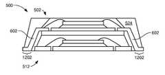
- FIG. 5therein is shown a cross-sectional view of a large integrated circuit package in package system 500 in an alternative embodiment of the present invention.
- the large integrated circuit package in package system 500may be greater than approximately 18 mm ⁇ 18 mm. Similar to the integrated circuit package in package system 100 of FIG. 1 , the large integrated circuit package in package system 500 includes an extended-lead integrated circuit package 502 .
- the extended-lead integrated circuit package 502includes extended leads 504 and an extended-lead die paddle 506 .
- a top integrated circuit die 508is attached and electrically connected to the extended-lead die paddle 506 .
- a lead-end surface 510is substantially planar and extends beyond a side opposite the top integrated circuit die 508 .
- the top integrated circuit die 508may provide functions, such as logic, processing or any combination thereof
- the top integrated circuit die 508is shown as a wire bondable integrated circuit die, although it is understood that the top integrated circuit die 508 may be different, such as a flip chip.
- the extended-lead integrated circuit package 502is shown with one integrated circuit die, although it is understood that any number of integrated circuit die may be included.
- the large integrated circuit package in package system 500also includes a base integrated circuit package 512 , such as a quad flat no lead or a land grid array, having base leads 514 and a base die paddle 516 .
- a bottom integrated circuit die 518is attached and electrically connected to the base die paddle 516 .
- a base surface 520is substantially planar on a side opposite the bottom integrated circuit die 518 .
- the bottom integrated circuit die 518may provide functions, such as flash memory, DRAM or any combination thereof, to the large integrated circuit package in package system 500 .
- the bottom integrated circuit die 518is shown as a wire bondable integrated circuit die, although it is understood that the bottom integrated circuit die 518 may be different, such as a flip chip.
- the base integrated circuit package 512is shown with one integrated circuit die, although it is understood that any number of integrated circuit die may be included.
- the extended-lead integrated circuit package 502is mounted over the base integrated circuit package 512 .
- a package-stacking layer 522holds the extended-lead integrated circuit package 502 and the base integrated circuit package 512 in a substantially fixed position.
- the lead-end surface 510 and the base surface 520are in substantially the same plane or coplanar.
- a package encapsulant 524such as a molding compound, may be applied to limit warpage for large size packages.
- the package encapsulant 524is flush or co-planar with the lead-end surface 510 and the base surface 520 .
- the extended leads 504provide electrical interconnectivity for the top integrated circuit die 508 in substantially the same plane as the base leads 514 for the bottom integrated circuit die 518 .
- the extended-lead integrated circuit package 502includes the extended leads 504 and the base integrated circuit package 512 includes the base leads 514 .
- the extended leads 504are held by the extended-lead integrated circuit package 502 and the package encapsulant 524 .
- the base leads 514are held substantially fixed by a base encapsulant 602 .
- the lead-end surface 510 of the extended leads 504 and the base surface 520 of the base leads 514provide a connection surface on the lower extent of the large integrated circuit package in package system 500 .
- the extended leads 504 and the base leads 514provide electrical interconnectivity to the next level system.
- the extended-lead integrated circuit package 502is shown with 40 of the extended leads 504 and the base integrated circuit package 512 is shown with 32 of the base leads 514 , although it is understood that any number of leads may be used.
- the extended-lead integrated circuit package 102includes the extended leads 104 and the extended-lead die paddle 106 .
- the extended leads 104 and the extended-lead die paddle 106are formed substantially planar without the need for a downset.
- a top die attach material 702attaches the top integrated circuit die 108 on the extended-lead die paddle 106 .
- Extended-lead connections 704such as wire bonds or solder bumps, electrically connect the top integrated circuit die 108 to the extended leads 104 .
- An extended-lead encapsulant 706covers the top integrated circuit die 108 , the extended-lead connections 704 , the extended-lead die paddle 106 and part of the extended leads 104 .
- An encapsulation processsuch as film-assist molding, applies the extended-lead encapsulant 706 flush or coplanar with the lead-end surface 110 and a bottom surface of the extended-lead die paddle 106 .
- the extended leads 104extend beyond the extents of the extended-lead encapsulant 706 .
- the extended-lead integrated circuit package 102may be tested as a discrete package.
- the testingincludes the top integrated circuit die 108 through the extended-lead connections 704 and the extended leads 104 .
- Functional tests as well as performance testsmay be performed on the extended-lead integrated circuit package 102 .
- Validating the integrity and performance of components in the packagingprovides a known good package with known good die.
- the known good packageimproves yield, reliability and quality of not only the integrated circuit package in package system 100 but also that of a next level system, such as a printed circuit board or another package.
- the base integrated circuit package 112includes the base leads 114 and the base die paddle 116 , which is optional.
- a bottom die attach material 802attaches the bottom integrated circuit die 118 on the base die paddle 116 .
- Base connections 804such as wire bonds or solder bumps, electrically connect the bottom integrated circuit die 118 to the base leads 114 .
- a base encapsulant 806covers the bottom integrated circuit die 118 , the base connections 804 , the base die paddle 116 and part of the base leads 114 .
- An encapsulation processsuch as film-assist molding, applies the base encapsulant 806 flush or coplanar with the base surface 120 and the bottom surface of the base die paddle 116 .
- the encapsulation processprovides the base surface 120 substantially exposed.
- the base integrated circuit package 112may be tested as a discrete package.
- the testingincludes the bottom integrated circuit die 118 through the base connections 804 and the base leads 114 .
- Functional tests as well as performance testsmay be performed on the base integrated circuit package 112 .
- Validating the integrity and performance of components in the packagingprovides a known good package with known good die.
- the known good packageimproves yield, reliability and quality of not only the integrated circuit package in package system 100 but also that of the next level system.
- the extended-lead integrated circuit package 102includes a bottom surface 902 .
- the base integrated circuit package 112includes a mold cap 904 formed by the base encapsulant 202 .
- the package-stacking layer 122such as an adhesive or an adhesive film, attaches the bottom surface 902 over the mold cap 904 .
- the extended-lead integrated circuit package 102 and the base integrated circuit package 112are held substantially fixed for further processing and attachment to the next level system.
- the package-stacking layer 122may also provide thermal or electrical properties, such as heat dissipation or electrical insulation.
- the extended-lead integrated circuit package 102includes the extended leads 104 having the lead-end surface 110 .
- the extended leads 104are further formed by a trim and form process by which the extended leads 104 may be cut and bent to a predetermined shape and a predetermined height.
- the extended leads 104are bent in a downward direction towards a side opposite the top integrated circuit die 108 and along the sides of the base integrated circuit package 112 .
- the extended leads 104provide the lead-end surface 110 substantially coplanar with the base surface 120 of the base integrated circuit package 112 .
- the extended leads 104may be substantially fixed in a small size package, less than approximately 10 mm ⁇ 10 mm, having substantially no package warpage.
- the top integrated circuit die 108connects through the extended-lead connections 704 and the extended leads 104 .
- the bottom integrated circuit die 118connects through the base connections 804 and the base leads 114 .
- the lead-end surface 110 of the extended leads 104 and the base surface 120 of the base leads 114provide a substantially planar electrical interconnectivity surface for the next level system, such as a printed circuit board.
- the medium integrated circuit package in package system 300may be a medium size package, approximately 10 mm ⁇ 10 mm to 18 mm ⁇ 18 mm. Some package warpage is possible with the medium size package.
- the lead-end encapsulant 324such as glob top or resin, may be applied to provide good planarity when warpage is possible. An encapsulating process may be used to apply the lead-end encapsulant 324 .
- the lead-end encapsulant 324covers the bottom of the base integrated circuit package 312 and the bottom of the extended-lead integrated circuit package 302 including lead ends 1102 of the extended leads 304 .
- the lead-end encapsulant 324provides a substantially fixed position for the extended leads 304 .
- the substantially fixed position of the extended leads 304provides isolation between each of the extended leads 304 as well as coplanarity between the extended leads and the base leads 314 .
- the large integrated circuit package in package system 500may be a large size package, greater than approximately 18 mm ⁇ 18 mm. Some package warpage is possible with the large size package.
- the package encapsulant 524such as molding compound, may be applied to provide good planarity when warpage is possible. An encapsulating process may be used to apply the package encapsulant 524 .
- the package encapsulant 524covers a portion of the base integrated circuit package 512 and a portion of the extended-lead integrated circuit package 502 including lead ends 1202 of the extended leads 504 .
- the package encapsulant 524provides a substantially fixed position for the extended leads 504 .
- the substantially fixed position of the extended leads 504provides isolation between each of the extended leads 504 as well as coplanarity between the extended leads and the base leads 514 .
- FIG. 13is a flow chart of an integrated circuit package in package system 1300 for manufacturing the integrated circuit package in package system 100 in an embodiment of the present invention.
- the system 1300includes forming a base integrated circuit package with a base lead having a portion with a substantially planar base surface in a block 1302 ; forming an extended-lead integrated circuit package with an extended lead having a portion with a substantially planar lead-end surface in a block 1304 ; and stacking the extended-lead integrated circuit package over the base integrated circuit package with the substantially planar lead-end surface coplanar with the substantially planar base surface in a block 1306 .
- a method to fabricate the integrated circuit package in package system 100is performed as follows:
- the present inventionprovides discrete integrated circuit packages in a 3D stack. Due to discrete integrated circuit packages, each of the integrated circuit packages may be tested individually.
- the integrated circuit packagesmay also contain one or more integrated circuits combined in one or some of several different interconnect or mounting processes.
- the disclosed structureprovides a smaller size.
- the footprint as well as areais more compact and space efficient.
- Multiple integrated circuit dieare efficiently placed over one another. It is particularly efficient in the critical dimensions for surface area with significant improvements over previous approaches.
Landscapes
- Engineering & Computer Science (AREA)
- Power Engineering (AREA)
- Microelectronics & Electronic Packaging (AREA)
- Physics & Mathematics (AREA)
- Condensed Matter Physics & Semiconductors (AREA)
- General Physics & Mathematics (AREA)
- Computer Hardware Design (AREA)
- Lead Frames For Integrated Circuits (AREA)
Abstract
Description
- 1. Forming a base integrated circuit package with a base surface of base leads substantially planar to one another and exposed. (
FIG. 8 ) - 2. Forming an extended-lead integrated circuit package with a lead-end surface of extended leads substantially planar to one another and exposed. (
FIG. 7 ) - 3. Stacking the extended-lead integrated circuit package over the base integrated circuit package with the lead-end surface coplanar with the base surface and having the lead-end surface and the base surface exposed for electrical connection. (
FIG. 10 )
- 1. Forming a base integrated circuit package with a base surface of base leads substantially planar to one another and exposed. (
Claims (10)
Priority Applications (1)
| Application Number | Priority Date | Filing Date | Title |
|---|---|---|---|
| US13/166,417US8164172B2 (en) | 2006-03-08 | 2011-06-22 | Integrated circuit package in package system |
Applications Claiming Priority (2)
| Application Number | Priority Date | Filing Date | Title |
|---|---|---|---|
| US11/276,647US7981702B2 (en) | 2006-03-08 | 2006-03-08 | Integrated circuit package in package system |
| US13/166,417US8164172B2 (en) | 2006-03-08 | 2011-06-22 | Integrated circuit package in package system |
Related Parent Applications (1)
| Application Number | Title | Priority Date | Filing Date |
|---|---|---|---|
| US11/276,647DivisionUS7981702B2 (en) | 2006-03-08 | 2006-03-08 | Integrated circuit package in package system |
Publications (2)
| Publication Number | Publication Date |
|---|---|
| US20110248411A1 US20110248411A1 (en) | 2011-10-13 |
| US8164172B2true US8164172B2 (en) | 2012-04-24 |
Family
ID=38478103
Family Applications (2)
| Application Number | Title | Priority Date | Filing Date |
|---|---|---|---|
| US11/276,647Active2027-09-09US7981702B2 (en) | 2006-03-08 | 2006-03-08 | Integrated circuit package in package system |
| US13/166,417ActiveUS8164172B2 (en) | 2006-03-08 | 2011-06-22 | Integrated circuit package in package system |
Family Applications Before (1)
| Application Number | Title | Priority Date | Filing Date |
|---|---|---|---|
| US11/276,647Active2027-09-09US7981702B2 (en) | 2006-03-08 | 2006-03-08 | Integrated circuit package in package system |
Country Status (1)
| Country | Link |
|---|---|
| US (2) | US7981702B2 (en) |
Cited By (1)
| Publication number | Priority date | Publication date | Assignee | Title |
|---|---|---|---|---|
| US20060138649A1 (en)* | 2002-10-08 | 2006-06-29 | Chippac, Inc. | Semiconductor multi-package module having inverted second package stacked over die-up flip-chip ball grid array (BGA) package |
Families Citing this family (17)
| Publication number | Priority date | Publication date | Assignee | Title |
|---|---|---|---|---|
| US7598606B2 (en)* | 2005-02-22 | 2009-10-06 | Stats Chippac Ltd. | Integrated circuit package system with die and package combination |
| US7981702B2 (en)* | 2006-03-08 | 2011-07-19 | Stats Chippac Ltd. | Integrated circuit package in package system |
| US7986043B2 (en)* | 2006-03-08 | 2011-07-26 | Stats Chippac Ltd. | Integrated circuit package on package system |
| US7969018B2 (en)* | 2008-07-15 | 2011-06-28 | Infineon Technologies Ag | Stacked semiconductor chips with separate encapsulations |
| JP2012069764A (en)* | 2010-09-24 | 2012-04-05 | On Semiconductor Trading Ltd | Circuit device and method for manufacturing the same |
| US9034692B2 (en) | 2011-03-21 | 2015-05-19 | Stats Chippac Ltd. | Integrated circuit packaging system with a flip chip and method of manufacture thereof |
| US8310098B2 (en) | 2011-05-16 | 2012-11-13 | Unigen Corporation | Switchable capacitor arrays for preventing power interruptions and extending backup power life |
| US9601417B2 (en)* | 2011-07-20 | 2017-03-21 | Unigen Corporation | “L” shaped lead integrated circuit package |
| US8564125B2 (en)* | 2011-09-02 | 2013-10-22 | Stats Chippac Ltd. | Integrated circuit packaging system with embedded thermal heat shield and method of manufacture thereof |
| US8951847B2 (en)* | 2012-01-18 | 2015-02-10 | Intersil Americas LLC | Package leadframe for dual side assembly |
| US10049977B2 (en)* | 2014-08-01 | 2018-08-14 | Qualcomm Incorporated | Semiconductor package on package structure and method of forming the same |
| US10504736B2 (en) | 2015-09-30 | 2019-12-10 | Texas Instruments Incorporated | Plating interconnect for silicon chip |
| US20170278825A1 (en)* | 2016-03-24 | 2017-09-28 | Freescale Semiconductor, Inc. | Apparatus and Methods for Multi-Die Packaging |
| WO2019066922A1 (en)* | 2017-09-29 | 2019-04-04 | Intel Corporation | Package on package assembly |
| US10418343B2 (en) | 2017-12-05 | 2019-09-17 | Infineon Technologies Ag | Package-in-package structure for semiconductor devices and methods of manufacture |
| US10840169B2 (en) | 2019-02-14 | 2020-11-17 | Amkor Technology Singapore Holding Pte. Ltd. | Semiconductor device and a method of manufacturing a semiconductor device |
| US20230245979A1 (en)* | 2022-02-01 | 2023-08-03 | Skyworks Solutions, Inc. | Shielded wafer level chip scale package with shield connected to ground via a seal ring |
Citations (74)
| Publication number | Priority date | Publication date | Assignee | Title |
|---|---|---|---|---|
| US4363076A (en)* | 1980-12-29 | 1982-12-07 | Honeywell Information Systems Inc. | Integrated circuit package |
| US5147815A (en) | 1990-05-14 | 1992-09-15 | Motorola, Inc. | Method for fabricating a multichip semiconductor device having two interdigitated leadframes |
| US5157480A (en) | 1991-02-06 | 1992-10-20 | Motorola, Inc. | Semiconductor device having dual electrical contact sites |
| US5222014A (en) | 1992-03-02 | 1993-06-22 | Motorola, Inc. | Three-dimensional multi-chip pad array carrier |
| US5394303A (en)* | 1992-09-11 | 1995-02-28 | Kabushiki Kaisha Toshiba | Semiconductor device |
| US5625228A (en) | 1995-02-27 | 1997-04-29 | Rogren; Philip E. | High performance semiconductor package with area array leads |
| US5685477A (en) | 1995-06-28 | 1997-11-11 | Intel Corporation | Method for attaching and handling conductive spheres to a substrate |
| US5773313A (en)* | 1992-10-20 | 1998-06-30 | Fujitsu Limited | Semiconductor device and method of producing the same |
| US5801439A (en)* | 1994-04-20 | 1998-09-01 | Fujitsu Limited | Semiconductor device and semiconductor device unit for a stack arrangement |
| US5835988A (en)* | 1996-03-27 | 1998-11-10 | Mitsubishi Denki Kabushiki Kaisha | Packed semiconductor device with wrap around external leads |
| US5877042A (en)* | 1996-08-28 | 1999-03-02 | Motorola, Inc. | Glass/Metal package and method for producing the same |
| US6084293A (en)* | 1997-07-25 | 2000-07-04 | Oki Electric Industry Co., Ltd. | Stacked semiconductor device |
| US6168975B1 (en) | 1998-06-24 | 2001-01-02 | St Assembly Test Services Pte Ltd | Method of forming extended lead package |
| US6190944B1 (en) | 1999-01-20 | 2001-02-20 | Hyundai Electronics Industries Co., Ltd. | Stacked package for semiconductor device and fabrication method thereof, and apparatus for making the stacked package |
| US6229200B1 (en) | 1998-06-10 | 2001-05-08 | Asat Limited | Saw-singulated leadless plastic chip carrier |
| US20020031865A1 (en)* | 1999-08-25 | 2002-03-14 | Tsung-Chieh Chen | Method for fabricating a dual-chip package and package formed |
| US20020041019A1 (en) | 2000-08-09 | 2002-04-11 | Gang Heung-Su | Semiconductor package having implantable conductive lands and method for manufacturing the same |
| US6420799B1 (en) | 1997-04-21 | 2002-07-16 | Hitachi, Ltd. | Power supply device for vehicles |
| US6420779B1 (en) | 1999-09-14 | 2002-07-16 | St Assembly Test Services Ltd. | Leadframe based chip scale package and method of producing the same |
| US6424031B1 (en)* | 2000-05-08 | 2002-07-23 | Amkor Technology, Inc. | Stackable package with heat sink |
| US20020100963A1 (en)* | 2001-01-26 | 2002-08-01 | Mitsubishi Denki Kabushiki Kaisha | Semiconductor package and semiconductor device |
| US20020105068A1 (en)* | 2001-02-05 | 2002-08-08 | Mitsubishi Denki Kabushiki Kaisha | Stacked semiconductor device structure |
| US6433418B1 (en)* | 1998-07-24 | 2002-08-13 | Fujitsu Limited | Apparatus for a vertically accumulable semiconductor device with external leads secured by a positioning mechanism |
| US20020109216A1 (en) | 2000-12-27 | 2002-08-15 | Yuko Matsuzaki | Integrated electronic device and integration method |
| US6445064B1 (en)* | 2001-02-06 | 2002-09-03 | Mitsubishi Denki Kabushiki Kaisha | Semiconductor device |
| US20020167074A1 (en) | 1999-04-17 | 2002-11-14 | Sun Dong Kim | Lead frame and bottom lead semiconductor package using the lead frame |
| US6500698B2 (en)* | 1998-10-24 | 2002-12-31 | Hynix Semiconductor, Inc. | Method for fabricating a stacked semiconductor chip package |
| US6559525B2 (en)* | 2000-01-13 | 2003-05-06 | Siliconware Precision Industries Co., Ltd. | Semiconductor package having heat sink at the outer surface |
| US6607937B1 (en) | 2000-08-23 | 2003-08-19 | Micron Technology, Inc. | Stacked microelectronic dies and methods for stacking microelectronic dies |
| US6624005B1 (en)* | 2000-09-06 | 2003-09-23 | Amkor Technology, Inc. | Semiconductor memory cards and method of making same |
| US20040012992A1 (en)* | 2002-07-16 | 2004-01-22 | Koh Wei H. | Multi-level package for a memory module |
| US20040056277A1 (en)* | 2002-09-17 | 2004-03-25 | Chippac, Inc. | Semiconductor multi-package module including stacked-die package and having wire bond interconnect between stacked packages |
| US20040061212A1 (en)* | 2002-09-17 | 2004-04-01 | Chippac, Inc. | Semiconductor multi-package module having wire bond interconnect between stacked packages |
| US20040061213A1 (en)* | 2002-09-17 | 2004-04-01 | Chippac, Inc. | Semiconductor multi-package module having package stacked over die-up flip chip ball grid array package and having wire bond interconnect between stacked packages |
| US20040063242A1 (en)* | 2002-09-17 | 2004-04-01 | Chippac, Inc. | Semiconductor multi-package module having package stacked over ball grid array package and having wire bond interconnect between stacked packages |
| US20040063246A1 (en)* | 2002-09-17 | 2004-04-01 | Chippac, Inc. | Semiconductor multi-package module having package stacked over die-down flip chip ball grid array package and having wire bond interconnect between stacked packages |
| US20040065963A1 (en)* | 2002-09-17 | 2004-04-08 | Chippac, Inc. | Semiconductor multi-package module having wire bond interconnect between stacked packages and having electrical shield |
| US6730544B1 (en)* | 1999-12-20 | 2004-05-04 | Amkor Technology, Inc. | Stackable semiconductor package and method for manufacturing same |
| US20040114426A1 (en) | 2001-08-06 | 2004-06-17 | Fee Setho Sing | Quad flat no-lead (QFN) grid array package, method of making and memory module and computer system including same |
| US6815806B1 (en) | 2003-07-17 | 2004-11-09 | International Business Machines Corp. | Asymmetric partially-etched leads for finer pitch semiconductor chip package |
| US20040227250A1 (en)* | 2003-05-12 | 2004-11-18 | Bolken Todd O. | Semiconductor component having stacked, encapsulated dice |
| US6838751B2 (en) | 2002-03-06 | 2005-01-04 | Freescale Semiconductor Inc. | Multi-row leadframe |
| US6861288B2 (en) | 2003-01-23 | 2005-03-01 | St Assembly Test Services, Ltd. | Stacked semiconductor packages and method for the fabrication thereof |
| US6906416B2 (en) | 2002-10-08 | 2005-06-14 | Chippac, Inc. | Semiconductor multi-package module having inverted second package stacked over die-up flip-chip ball grid array (BGA) package |
| US20050133897A1 (en) | 2003-12-17 | 2005-06-23 | Baek Joong-Hyun | Stack package with improved heat radiation and module having the stack package mounted thereon |
| US6917097B2 (en) | 2003-07-15 | 2005-07-12 | Freescale Semiconductor, Inc. | Dual gauge leadframe |
| US20050161806A1 (en)* | 2004-01-22 | 2005-07-28 | Divakar Mysore P. | Area array packages with overmolded pin-fin heat sinks |
| US6927096B2 (en) | 2002-11-15 | 2005-08-09 | Renesas Technology Corp. | Method of manufacturing a semiconductor device |
| US20050253224A1 (en)* | 2004-05-11 | 2005-11-17 | Via Technologies, Inc. | Stacked multi-chip package |
| US6977431B1 (en)* | 2003-11-05 | 2005-12-20 | Amkor Technology, Inc. | Stackable semiconductor package and manufacturing method thereof |
| US20060001136A1 (en)* | 2004-06-30 | 2006-01-05 | Advanced Semiconductor Engineering, Inc. | Quad flat non-leaded package |
| US20060046531A1 (en) | 2004-08-27 | 2006-03-02 | Aries Electronics, Inc. | Top loaded burn-in socket |
| US20060055009A1 (en)* | 2004-06-10 | 2006-03-16 | Stats Chippac Ltd. | Chip scale package with open substrate |
| US20060091516A1 (en)* | 2004-11-01 | 2006-05-04 | Akira Matsunami | Flexible leaded stacked semiconductor package |
| US7042068B2 (en)* | 2000-04-27 | 2006-05-09 | Amkor Technology, Inc. | Leadframe and semiconductor package made using the leadframe |
| US7190062B1 (en)* | 2004-06-15 | 2007-03-13 | Amkor Technology, Inc. | Embedded leadframe semiconductor package |
| US7227249B1 (en)* | 2003-12-24 | 2007-06-05 | Bridge Semiconductor Corporation | Three-dimensional stacked semiconductor package with chips on opposite sides of lead |
| US7245007B1 (en)* | 2003-09-18 | 2007-07-17 | Amkor Technology, Inc. | Exposed lead interposer leadframe package |
| US7247934B2 (en) | 2004-11-16 | 2007-07-24 | Siliconware Precision Industries Co., Ltd. | Multi-chip semiconductor package |
| US7253511B2 (en) | 2004-07-13 | 2007-08-07 | Chippac, Inc. | Semiconductor multipackage module including die and inverted land grid array package stacked over ball grid array package |
| US20070210424A1 (en) | 2006-03-08 | 2007-09-13 | Stats Chippac Ltd. | Integrated circuit package in package system |
| US20070209834A1 (en) | 2006-03-08 | 2007-09-13 | Stats Chippac Ltd. | Integrated circuit leaded stacked package system |
| US20070210443A1 (en) | 2006-03-08 | 2007-09-13 | Stats Chippac Ltd. | Integrated circuit package on package system |
| US20070247614A1 (en) | 2004-10-06 | 2007-10-25 | Puah Yong J | System for 2-D and 3-D Vision Inspection |
| US7291926B2 (en) | 2003-12-31 | 2007-11-06 | Advanced Semiconductor Engineering, Inc. | Multi-chip package structure |
| US7361533B1 (en)* | 2002-11-08 | 2008-04-22 | Amkor Technology, Inc. | Stacked embedded leadframe |
| US7372141B2 (en) | 2005-03-31 | 2008-05-13 | Stats Chippac Ltd. | Semiconductor stacked package assembly having exposed substrate surfaces on upper and lower sides |
| US7394148B2 (en) | 2005-06-20 | 2008-07-01 | Stats Chippac Ltd. | Module having stacked chip scale semiconductor packages |
| US7429786B2 (en) | 2005-04-29 | 2008-09-30 | Stats Chippac Ltd. | Semiconductor package including second substrate and having exposed substrate surfaces on upper and lower sides |
| US7429787B2 (en) | 2005-03-31 | 2008-09-30 | Stats Chippac Ltd. | Semiconductor assembly including chip scale package and second substrate with exposed surfaces on upper and lower sides |
| US7598606B2 (en)* | 2005-02-22 | 2009-10-06 | Stats Chippac Ltd. | Integrated circuit package system with die and package combination |
| US7622332B2 (en) | 2002-04-29 | 2009-11-24 | Unisem (Mauritius) Holdings Limited | Partially patterned lead frames and methods of making and using the same in semiconductor packaging |
| US7629677B2 (en)* | 2006-09-21 | 2009-12-08 | Samsung Electronics Co., Ltd. | Semiconductor package with inner leads exposed from an encapsulant |
| US8053883B2 (en)* | 2008-07-23 | 2011-11-08 | Fairchild Semiconductor Corporation | Isolated stacked die semiconductor packages |
- 2006
- 2006-03-08USUS11/276,647patent/US7981702B2/enactiveActive
- 2011
- 2011-06-22USUS13/166,417patent/US8164172B2/enactiveActive
Patent Citations (94)
| Publication number | Priority date | Publication date | Assignee | Title |
|---|---|---|---|---|
| US4363076A (en)* | 1980-12-29 | 1982-12-07 | Honeywell Information Systems Inc. | Integrated circuit package |
| US5147815A (en) | 1990-05-14 | 1992-09-15 | Motorola, Inc. | Method for fabricating a multichip semiconductor device having two interdigitated leadframes |
| US5157480A (en) | 1991-02-06 | 1992-10-20 | Motorola, Inc. | Semiconductor device having dual electrical contact sites |
| US5222014A (en) | 1992-03-02 | 1993-06-22 | Motorola, Inc. | Three-dimensional multi-chip pad array carrier |
| US5394303A (en)* | 1992-09-11 | 1995-02-28 | Kabushiki Kaisha Toshiba | Semiconductor device |
| US5773313A (en)* | 1992-10-20 | 1998-06-30 | Fujitsu Limited | Semiconductor device and method of producing the same |
| US5801439A (en)* | 1994-04-20 | 1998-09-01 | Fujitsu Limited | Semiconductor device and semiconductor device unit for a stack arrangement |
| US5625228A (en) | 1995-02-27 | 1997-04-29 | Rogren; Philip E. | High performance semiconductor package with area array leads |
| US5685477A (en) | 1995-06-28 | 1997-11-11 | Intel Corporation | Method for attaching and handling conductive spheres to a substrate |
| US5835988A (en)* | 1996-03-27 | 1998-11-10 | Mitsubishi Denki Kabushiki Kaisha | Packed semiconductor device with wrap around external leads |
| US5877042A (en)* | 1996-08-28 | 1999-03-02 | Motorola, Inc. | Glass/Metal package and method for producing the same |
| US6420799B1 (en) | 1997-04-21 | 2002-07-16 | Hitachi, Ltd. | Power supply device for vehicles |
| US6084293A (en)* | 1997-07-25 | 2000-07-04 | Oki Electric Industry Co., Ltd. | Stacked semiconductor device |
| US6229200B1 (en) | 1998-06-10 | 2001-05-08 | Asat Limited | Saw-singulated leadless plastic chip carrier |
| US6168975B1 (en) | 1998-06-24 | 2001-01-02 | St Assembly Test Services Pte Ltd | Method of forming extended lead package |
| US6433418B1 (en)* | 1998-07-24 | 2002-08-13 | Fujitsu Limited | Apparatus for a vertically accumulable semiconductor device with external leads secured by a positioning mechanism |
| US6500698B2 (en)* | 1998-10-24 | 2002-12-31 | Hynix Semiconductor, Inc. | Method for fabricating a stacked semiconductor chip package |
| US6190944B1 (en) | 1999-01-20 | 2001-02-20 | Hyundai Electronics Industries Co., Ltd. | Stacked package for semiconductor device and fabrication method thereof, and apparatus for making the stacked package |
| US20020167074A1 (en) | 1999-04-17 | 2002-11-14 | Sun Dong Kim | Lead frame and bottom lead semiconductor package using the lead frame |
| US20020031865A1 (en)* | 1999-08-25 | 2002-03-14 | Tsung-Chieh Chen | Method for fabricating a dual-chip package and package formed |
| US6420779B1 (en) | 1999-09-14 | 2002-07-16 | St Assembly Test Services Ltd. | Leadframe based chip scale package and method of producing the same |
| US6730544B1 (en)* | 1999-12-20 | 2004-05-04 | Amkor Technology, Inc. | Stackable semiconductor package and method for manufacturing same |
| US6559525B2 (en)* | 2000-01-13 | 2003-05-06 | Siliconware Precision Industries Co., Ltd. | Semiconductor package having heat sink at the outer surface |
| US7042068B2 (en)* | 2000-04-27 | 2006-05-09 | Amkor Technology, Inc. | Leadframe and semiconductor package made using the leadframe |
| US6424031B1 (en)* | 2000-05-08 | 2002-07-23 | Amkor Technology, Inc. | Stackable package with heat sink |
| US20020041019A1 (en) | 2000-08-09 | 2002-04-11 | Gang Heung-Su | Semiconductor package having implantable conductive lands and method for manufacturing the same |
| US6607937B1 (en) | 2000-08-23 | 2003-08-19 | Micron Technology, Inc. | Stacked microelectronic dies and methods for stacking microelectronic dies |
| US7235871B2 (en) | 2000-08-23 | 2007-06-26 | Micron Technology, Inc. | Stacked microelectronic dies |
| US6624005B1 (en)* | 2000-09-06 | 2003-09-23 | Amkor Technology, Inc. | Semiconductor memory cards and method of making same |
| US20020109216A1 (en) | 2000-12-27 | 2002-08-15 | Yuko Matsuzaki | Integrated electronic device and integration method |
| US20020100963A1 (en)* | 2001-01-26 | 2002-08-01 | Mitsubishi Denki Kabushiki Kaisha | Semiconductor package and semiconductor device |
| US20030127729A1 (en)* | 2001-02-05 | 2003-07-10 | Takakazu Fukumoto | Stacked semiconductor device structure |
| US20020105068A1 (en)* | 2001-02-05 | 2002-08-08 | Mitsubishi Denki Kabushiki Kaisha | Stacked semiconductor device structure |
| US6445064B1 (en)* | 2001-02-06 | 2002-09-03 | Mitsubishi Denki Kabushiki Kaisha | Semiconductor device |
| US20040114426A1 (en) | 2001-08-06 | 2004-06-17 | Fee Setho Sing | Quad flat no-lead (QFN) grid array package, method of making and memory module and computer system including same |
| US6838751B2 (en) | 2002-03-06 | 2005-01-04 | Freescale Semiconductor Inc. | Multi-row leadframe |
| US7622332B2 (en) | 2002-04-29 | 2009-11-24 | Unisem (Mauritius) Holdings Limited | Partially patterned lead frames and methods of making and using the same in semiconductor packaging |
| US20040012992A1 (en)* | 2002-07-16 | 2004-01-22 | Koh Wei H. | Multi-level package for a memory module |
| US20040061213A1 (en)* | 2002-09-17 | 2004-04-01 | Chippac, Inc. | Semiconductor multi-package module having package stacked over die-up flip chip ball grid array package and having wire bond interconnect between stacked packages |
| US20040063242A1 (en)* | 2002-09-17 | 2004-04-01 | Chippac, Inc. | Semiconductor multi-package module having package stacked over ball grid array package and having wire bond interconnect between stacked packages |
| US20040065963A1 (en)* | 2002-09-17 | 2004-04-08 | Chippac, Inc. | Semiconductor multi-package module having wire bond interconnect between stacked packages and having electrical shield |
| US20040056277A1 (en)* | 2002-09-17 | 2004-03-25 | Chippac, Inc. | Semiconductor multi-package module including stacked-die package and having wire bond interconnect between stacked packages |
| US20040063246A1 (en)* | 2002-09-17 | 2004-04-01 | Chippac, Inc. | Semiconductor multi-package module having package stacked over die-down flip chip ball grid array package and having wire bond interconnect between stacked packages |
| US20040061212A1 (en)* | 2002-09-17 | 2004-04-01 | Chippac, Inc. | Semiconductor multi-package module having wire bond interconnect between stacked packages |
| US7057269B2 (en) | 2002-10-08 | 2006-06-06 | Chippac, Inc. | Semiconductor multi-package module having inverted land grid array (LGA) package stacked over ball grid array (BGA) package |
| US7358115B2 (en) | 2002-10-08 | 2008-04-15 | Chippac, Inc. | Method of fabricating a semiconductor assembly including chip scale package and second substrate with exposed substrate surfaces on upper and lower sides |
| US7247519B2 (en) | 2002-10-08 | 2007-07-24 | Chippac, Inc. | Method for making a semiconductor multi-package module having inverted bump chip carrier second package |
| US7101731B2 (en) | 2002-10-08 | 2006-09-05 | Chippac, Inc. | Semiconductor multi-package module having inverted second package stacked over die-up flip-chip ball grid array (BGA) package |
| US7061088B2 (en) | 2002-10-08 | 2006-06-13 | Chippac, Inc. | Semiconductor stacked multi-package module having inverted second package |
| US6933598B2 (en) | 2002-10-08 | 2005-08-23 | Chippac, Inc. | Semiconductor stacked multi-package module having inverted second package and electrically shielded first package |
| US7364946B2 (en) | 2002-10-08 | 2008-04-29 | Chippac, Inc. | Method of fabricating a semiconductor multi-package module having inverted land grid array (LGA) package stacked over ball grid array (BGA) package |
| US7169642B2 (en) | 2002-10-08 | 2007-01-30 | Chippac, Inc | Method of fabricating a semiconductor multi-package module having inverted land grid array (LGA) package stacked over ball grid array (BGA) package |
| US7163842B2 (en) | 2002-10-08 | 2007-01-16 | Chip Pac, Inc. | Method of fabricating a semiconductor multi-package module having inverted second package stacked over die-up flip-chip ball grid array (BGA) |
| US6906416B2 (en) | 2002-10-08 | 2005-06-14 | Chippac, Inc. | Semiconductor multi-package module having inverted second package stacked over die-up flip-chip ball grid array (BGA) package |
| US7351610B2 (en) | 2002-10-08 | 2008-04-01 | Chippac, Inc. | Method of fabricating a semiconductor multi-package module having a second package substrate with an exposed metal layer wire bonded to a first package substrate |
| US7288434B2 (en) | 2002-10-08 | 2007-10-30 | Chippac, Inc. | Method for making semiconductor multi-package module having inverted second package and including additional die or package stacked on second package |
| US7166494B2 (en) | 2002-10-08 | 2007-01-23 | Chippac, Inc. | Method of fabricating a semiconductor stacked multi-package module having inverted second package |
| US7045887B2 (en) | 2002-10-08 | 2006-05-16 | Chippac, Inc. | Semiconductor multi-package module having inverted second package stacked over die-up flip-chip ball grid array (BGA) package |
| US7049691B2 (en) | 2002-10-08 | 2006-05-23 | Chippac, Inc. | Semiconductor multi-package module having inverted second package and including additional die or stacked package on second package |
| US7053477B2 (en) | 2002-10-08 | 2006-05-30 | Chippac, Inc. | Semiconductor multi-package module having inverted bump chip carrier second package |
| US7361533B1 (en)* | 2002-11-08 | 2008-04-22 | Amkor Technology, Inc. | Stacked embedded leadframe |
| US6927096B2 (en) | 2002-11-15 | 2005-08-09 | Renesas Technology Corp. | Method of manufacturing a semiconductor device |
| US6861288B2 (en) | 2003-01-23 | 2005-03-01 | St Assembly Test Services, Ltd. | Stacked semiconductor packages and method for the fabrication thereof |
| US7109576B2 (en)* | 2003-05-12 | 2006-09-19 | Micron Technology, Inc. | Semiconductor component having encapsulated die stack |
| US20040227250A1 (en)* | 2003-05-12 | 2004-11-18 | Bolken Todd O. | Semiconductor component having stacked, encapsulated dice |
| US7227252B2 (en)* | 2003-05-12 | 2007-06-05 | Micron Technology, Inc. | Semiconductor component having stacked, encapsulated dice and method of fabrication |
| US6917097B2 (en) | 2003-07-15 | 2005-07-12 | Freescale Semiconductor, Inc. | Dual gauge leadframe |
| US6815806B1 (en) | 2003-07-17 | 2004-11-09 | International Business Machines Corp. | Asymmetric partially-etched leads for finer pitch semiconductor chip package |
| US7245007B1 (en)* | 2003-09-18 | 2007-07-17 | Amkor Technology, Inc. | Exposed lead interposer leadframe package |
| US6977431B1 (en)* | 2003-11-05 | 2005-12-20 | Amkor Technology, Inc. | Stackable semiconductor package and manufacturing method thereof |
| US20050133897A1 (en) | 2003-12-17 | 2005-06-23 | Baek Joong-Hyun | Stack package with improved heat radiation and module having the stack package mounted thereon |
| US7227249B1 (en)* | 2003-12-24 | 2007-06-05 | Bridge Semiconductor Corporation | Three-dimensional stacked semiconductor package with chips on opposite sides of lead |
| US7291926B2 (en) | 2003-12-31 | 2007-11-06 | Advanced Semiconductor Engineering, Inc. | Multi-chip package structure |
| US20050161806A1 (en)* | 2004-01-22 | 2005-07-28 | Divakar Mysore P. | Area array packages with overmolded pin-fin heat sinks |
| US7180166B2 (en) | 2004-05-11 | 2007-02-20 | Via Technologies, Inc. | Stacked multi-chip package |
| US20050253224A1 (en)* | 2004-05-11 | 2005-11-17 | Via Technologies, Inc. | Stacked multi-chip package |
| US20060055009A1 (en)* | 2004-06-10 | 2006-03-16 | Stats Chippac Ltd. | Chip scale package with open substrate |
| US7190062B1 (en)* | 2004-06-15 | 2007-03-13 | Amkor Technology, Inc. | Embedded leadframe semiconductor package |
| US20060001136A1 (en)* | 2004-06-30 | 2006-01-05 | Advanced Semiconductor Engineering, Inc. | Quad flat non-leaded package |
| US7253511B2 (en) | 2004-07-13 | 2007-08-07 | Chippac, Inc. | Semiconductor multipackage module including die and inverted land grid array package stacked over ball grid array package |
| US20060046531A1 (en) | 2004-08-27 | 2006-03-02 | Aries Electronics, Inc. | Top loaded burn-in socket |
| US20070247614A1 (en) | 2004-10-06 | 2007-10-25 | Puah Yong J | System for 2-D and 3-D Vision Inspection |
| US20060091516A1 (en)* | 2004-11-01 | 2006-05-04 | Akira Matsunami | Flexible leaded stacked semiconductor package |
| US7247934B2 (en) | 2004-11-16 | 2007-07-24 | Siliconware Precision Industries Co., Ltd. | Multi-chip semiconductor package |
| US7598606B2 (en)* | 2005-02-22 | 2009-10-06 | Stats Chippac Ltd. | Integrated circuit package system with die and package combination |
| US7372141B2 (en) | 2005-03-31 | 2008-05-13 | Stats Chippac Ltd. | Semiconductor stacked package assembly having exposed substrate surfaces on upper and lower sides |
| US7429787B2 (en) | 2005-03-31 | 2008-09-30 | Stats Chippac Ltd. | Semiconductor assembly including chip scale package and second substrate with exposed surfaces on upper and lower sides |
| US7429786B2 (en) | 2005-04-29 | 2008-09-30 | Stats Chippac Ltd. | Semiconductor package including second substrate and having exposed substrate surfaces on upper and lower sides |
| US7394148B2 (en) | 2005-06-20 | 2008-07-01 | Stats Chippac Ltd. | Module having stacked chip scale semiconductor packages |
| US20070210443A1 (en) | 2006-03-08 | 2007-09-13 | Stats Chippac Ltd. | Integrated circuit package on package system |
| US20070209834A1 (en) | 2006-03-08 | 2007-09-13 | Stats Chippac Ltd. | Integrated circuit leaded stacked package system |
| US20070210424A1 (en) | 2006-03-08 | 2007-09-13 | Stats Chippac Ltd. | Integrated circuit package in package system |
| US7629677B2 (en)* | 2006-09-21 | 2009-12-08 | Samsung Electronics Co., Ltd. | Semiconductor package with inner leads exposed from an encapsulant |
| US8053883B2 (en)* | 2008-07-23 | 2011-11-08 | Fairchild Semiconductor Corporation | Isolated stacked die semiconductor packages |
Cited By (1)
| Publication number | Priority date | Publication date | Assignee | Title |
|---|---|---|---|---|
| US20060138649A1 (en)* | 2002-10-08 | 2006-06-29 | Chippac, Inc. | Semiconductor multi-package module having inverted second package stacked over die-up flip-chip ball grid array (BGA) package |
Also Published As
| Publication number | Publication date |
|---|---|
| US7981702B2 (en) | 2011-07-19 |
| US20110248411A1 (en) | 2011-10-13 |
| US20070210424A1 (en) | 2007-09-13 |
Similar Documents
| Publication | Publication Date | Title |
|---|---|---|
| US8164172B2 (en) | Integrated circuit package in package system | |
| US8513542B2 (en) | Integrated circuit leaded stacked package system | |
| US7986043B2 (en) | Integrated circuit package on package system | |
| US6861288B2 (en) | Stacked semiconductor packages and method for the fabrication thereof | |
| US7298038B2 (en) | Integrated circuit package system including die stacking | |
| US8592973B2 (en) | Integrated circuit packaging system with package-on-package stacking and method of manufacture thereof | |
| US7968996B2 (en) | Integrated circuit package system with supported stacked die | |
| US8334171B2 (en) | Package system with a shielded inverted internal stacking module and method of manufacture thereof | |
| US8203214B2 (en) | Integrated circuit package in package system with adhesiveless package attach | |
| US7750482B2 (en) | Integrated circuit package system including zero fillet resin | |
| US8759954B2 (en) | Integrated circuit package system with offset stacked die | |
| US20080315406A1 (en) | Integrated circuit package system with cavity substrate | |
| US20080185702A1 (en) | Multi-chip package system with multiple substrates | |
| KR20130129896A (en) | Method and system for thin multi chip stack package with film on wire and copper wire | |
| US8062934B2 (en) | Integrated circuit package system with ground bonds | |
| US8633578B2 (en) | Integrated circuit package system with laminate base | |
| US7667314B2 (en) | Integrated circuit package system with mold lock subassembly | |
| US20070085184A1 (en) | Stacked die packaging system | |
| US20080303123A1 (en) | Integrated circuit package system with leadfinger |
Legal Events
| Date | Code | Title | Description |
|---|---|---|---|
| STCF | Information on status: patent grant | Free format text:PATENTED CASE | |
| CC | Certificate of correction | ||
| AS | Assignment | Owner name:CITICORP INTERNATIONAL LIMITED, AS COMMON SECURITY AGENT, HONG KONG Free format text:SECURITY INTEREST;ASSIGNORS:STATS CHIPPAC, INC.;STATS CHIPPAC LTD.;REEL/FRAME:036288/0748 Effective date:20150806 Owner name:CITICORP INTERNATIONAL LIMITED, AS COMMON SECURITY Free format text:SECURITY INTEREST;ASSIGNORS:STATS CHIPPAC, INC.;STATS CHIPPAC LTD.;REEL/FRAME:036288/0748 Effective date:20150806 | |
| FPAY | Fee payment | Year of fee payment:4 | |
| AS | Assignment | Owner name:STATS CHIPPAC PTE. LTE., SINGAPORE Free format text:CHANGE OF NAME;ASSIGNOR:STATS CHIPPAC LTD.;REEL/FRAME:038378/0280 Effective date:20160329 | |
| MAFP | Maintenance fee payment | Free format text:PAYMENT OF MAINTENANCE FEE, 8TH YEAR, LARGE ENTITY (ORIGINAL EVENT CODE: M1552); ENTITY STATUS OF PATENT OWNER: LARGE ENTITY Year of fee payment:8 | |
| AS | Assignment | Owner name:STATS CHIPPAC PTE. LTD. FORMERLY KNOWN AS STATS CHIPPAC LTD., SINGAPORE Free format text:RELEASE BY SECURED PARTY;ASSIGNOR:CITICORP INTERNATIONAL LIMITED, AS COMMON SECURITY AGENT;REEL/FRAME:052864/0057 Effective date:20190503 Owner name:STATS CHIPPAC, INC., CALIFORNIA Free format text:RELEASE BY SECURED PARTY;ASSIGNOR:CITICORP INTERNATIONAL LIMITED, AS COMMON SECURITY AGENT;REEL/FRAME:052864/0057 Effective date:20190503 | |
| AS | Assignment | Owner name:STATS CHIPPAC PTE. LTE., SINGAPORE Free format text:CORRECT ERROR IN ASSIGNMENT NAME FROM STATS CHIPPAC PTE. LTE. TO STATS CHIPPAC PTE. LTD. (REEL: 38378 FRAME: 0280);ASSIGNOR:STATS CHIPPAC LTD.;REEL/FRAME:064789/0474 Effective date:20160329 | |
| AS | Assignment | Owner name:STATS CHIPPAC PTE. LTD., SINGAPORE Free format text:CORRECTIVE ASSIGNMENT TO CORRECT THE RECEIVING PARTY NAME PREVIOUSLY RECORDED AT REEL: 064789 FRAME: 0474 ASSIGNOR(S) HEREBY CONFIRMS THE CHANGE OF NAME;ASSIGNOR:STATS CHIPPAC LTD.;REEL/FRAME:064842/0046 Effective date:20160329 | |
| MAFP | Maintenance fee payment | Free format text:PAYMENT OF MAINTENANCE FEE, 12TH YEAR, LARGE ENTITY (ORIGINAL EVENT CODE: M1553); ENTITY STATUS OF PATENT OWNER: LARGE ENTITY Year of fee payment:12 |