US8163580B2 - Multiple die LED and lens optical system - Google Patents
Multiple die LED and lens optical systemDownload PDFInfo
- Publication number
- US8163580B2 US8163580B2US11/201,465US20146505AUS8163580B2US 8163580 B2US8163580 B2US 8163580B2US 20146505 AUS20146505 AUS 20146505AUS 8163580 B2US8163580 B2US 8163580B2
- Authority
- US
- United States
- Prior art keywords
- light emitting
- emitting diode
- lens
- submount
- diode dies
- Prior art date
- Legal status (The legal status is an assumption and is not a legal conclusion. Google has not performed a legal analysis and makes no representation as to the accuracy of the status listed.)
- Active, expires
Links
Images


Classifications
- H—ELECTRICITY
- H10—SEMICONDUCTOR DEVICES; ELECTRIC SOLID-STATE DEVICES NOT OTHERWISE PROVIDED FOR
- H10H—INORGANIC LIGHT-EMITTING SEMICONDUCTOR DEVICES HAVING POTENTIAL BARRIERS
- H10H20/00—Individual inorganic light-emitting semiconductor devices having potential barriers, e.g. light-emitting diodes [LED]
- H10H20/80—Constructional details
- H10H20/85—Packages
- H10H20/855—Optical field-shaping means, e.g. lenses
- G—PHYSICS
- G03—PHOTOGRAPHY; CINEMATOGRAPHY; ANALOGOUS TECHNIQUES USING WAVES OTHER THAN OPTICAL WAVES; ELECTROGRAPHY; HOLOGRAPHY
- G03B—APPARATUS OR ARRANGEMENTS FOR TAKING PHOTOGRAPHS OR FOR PROJECTING OR VIEWING THEM; APPARATUS OR ARRANGEMENTS EMPLOYING ANALOGOUS TECHNIQUES USING WAVES OTHER THAN OPTICAL WAVES; ACCESSORIES THEREFOR
- G03B15/00—Special procedures for taking photographs; Apparatus therefor
- G03B15/02—Illuminating scene
- G03B15/03—Combinations of cameras with lighting apparatus; Flash units
- H—ELECTRICITY
- H01—ELECTRIC ELEMENTS
- H01L—SEMICONDUCTOR DEVICES NOT COVERED BY CLASS H10
- H01L25/00—Assemblies consisting of a plurality of semiconductor or other solid state devices
- H01L25/03—Assemblies consisting of a plurality of semiconductor or other solid state devices all the devices being of a type provided for in a single subclass of subclasses H10B, H10D, H10F, H10H, H10K or H10N, e.g. assemblies of rectifier diodes
- H01L25/04—Assemblies consisting of a plurality of semiconductor or other solid state devices all the devices being of a type provided for in a single subclass of subclasses H10B, H10D, H10F, H10H, H10K or H10N, e.g. assemblies of rectifier diodes the devices not having separate containers
- H01L25/075—Assemblies consisting of a plurality of semiconductor or other solid state devices all the devices being of a type provided for in a single subclass of subclasses H10B, H10D, H10F, H10H, H10K or H10N, e.g. assemblies of rectifier diodes the devices not having separate containers the devices being of a type provided for in group H10H20/00
- H01L25/0753—Assemblies consisting of a plurality of semiconductor or other solid state devices all the devices being of a type provided for in a single subclass of subclasses H10B, H10D, H10F, H10H, H10K or H10N, e.g. assemblies of rectifier diodes the devices not having separate containers the devices being of a type provided for in group H10H20/00 the devices being arranged next to each other
- H—ELECTRICITY
- H04—ELECTRIC COMMUNICATION TECHNIQUE
- H04N—PICTORIAL COMMUNICATION, e.g. TELEVISION
- H04N23/00—Cameras or camera modules comprising electronic image sensors; Control thereof
- H04N23/56—Cameras or camera modules comprising electronic image sensors; Control thereof provided with illuminating means
- G—PHYSICS
- G03—PHOTOGRAPHY; CINEMATOGRAPHY; ANALOGOUS TECHNIQUES USING WAVES OTHER THAN OPTICAL WAVES; ELECTROGRAPHY; HOLOGRAPHY
- G03B—APPARATUS OR ARRANGEMENTS FOR TAKING PHOTOGRAPHS OR FOR PROJECTING OR VIEWING THEM; APPARATUS OR ARRANGEMENTS EMPLOYING ANALOGOUS TECHNIQUES USING WAVES OTHER THAN OPTICAL WAVES; ACCESSORIES THEREFOR
- G03B2215/00—Special procedures for taking photographs; Apparatus therefor
- G03B2215/05—Combinations of cameras with electronic flash units
- G03B2215/0503—Built-in units
- G—PHYSICS
- G03—PHOTOGRAPHY; CINEMATOGRAPHY; ANALOGOUS TECHNIQUES USING WAVES OTHER THAN OPTICAL WAVES; ELECTROGRAPHY; HOLOGRAPHY
- G03B—APPARATUS OR ARRANGEMENTS FOR TAKING PHOTOGRAPHS OR FOR PROJECTING OR VIEWING THEM; APPARATUS OR ARRANGEMENTS EMPLOYING ANALOGOUS TECHNIQUES USING WAVES OTHER THAN OPTICAL WAVES; ACCESSORIES THEREFOR
- G03B2215/00—Special procedures for taking photographs; Apparatus therefor
- G03B2215/05—Combinations of cameras with electronic flash units
- G03B2215/0564—Combinations of cameras with electronic flash units characterised by the type of light source
- G03B2215/0567—Solid-state light source, e.g. LED, laser
- G—PHYSICS
- G03—PHOTOGRAPHY; CINEMATOGRAPHY; ANALOGOUS TECHNIQUES USING WAVES OTHER THAN OPTICAL WAVES; ELECTROGRAPHY; HOLOGRAPHY
- G03B—APPARATUS OR ARRANGEMENTS FOR TAKING PHOTOGRAPHS OR FOR PROJECTING OR VIEWING THEM; APPARATUS OR ARRANGEMENTS EMPLOYING ANALOGOUS TECHNIQUES USING WAVES OTHER THAN OPTICAL WAVES; ACCESSORIES THEREFOR
- G03B2215/00—Special procedures for taking photographs; Apparatus therefor
- G03B2215/05—Combinations of cameras with electronic flash units
- G03B2215/0564—Combinations of cameras with electronic flash units characterised by the type of light source
- G03B2215/0571—With second light source
- H—ELECTRICITY
- H01—ELECTRIC ELEMENTS
- H01L—SEMICONDUCTOR DEVICES NOT COVERED BY CLASS H10
- H01L2224/00—Indexing scheme for arrangements for connecting or disconnecting semiconductor or solid-state bodies and methods related thereto as covered by H01L24/00
- H01L2224/01—Means for bonding being attached to, or being formed on, the surface to be connected, e.g. chip-to-package, die-attach, "first-level" interconnects; Manufacturing methods related thereto
- H01L2224/10—Bump connectors; Manufacturing methods related thereto
- H01L2224/15—Structure, shape, material or disposition of the bump connectors after the connecting process
- H01L2224/16—Structure, shape, material or disposition of the bump connectors after the connecting process of an individual bump connector
- H01L2224/161—Disposition
- H01L2224/16151—Disposition the bump connector connecting between a semiconductor or solid-state body and an item not being a semiconductor or solid-state body, e.g. chip-to-substrate, chip-to-passive
- H01L2224/16221—Disposition the bump connector connecting between a semiconductor or solid-state body and an item not being a semiconductor or solid-state body, e.g. chip-to-substrate, chip-to-passive the body and the item being stacked
- H01L2224/16225—Disposition the bump connector connecting between a semiconductor or solid-state body and an item not being a semiconductor or solid-state body, e.g. chip-to-substrate, chip-to-passive the body and the item being stacked the item being non-metallic, e.g. insulating substrate with or without metallisation
- H—ELECTRICITY
- H01—ELECTRIC ELEMENTS
- H01L—SEMICONDUCTOR DEVICES NOT COVERED BY CLASS H10
- H01L2924/00—Indexing scheme for arrangements or methods for connecting or disconnecting semiconductor or solid-state bodies as covered by H01L24/00
- H01L2924/0001—Technical content checked by a classifier
- H01L2924/0002—Not covered by any one of groups H01L24/00, H01L24/00 and H01L2224/00
Definitions
- the present inventionrelates generally to light emitting diodes and more particularly to increasing the light on target from light emitting diodes.
- LED deviceshave ever increasing applications. Devices that are capable of generating white light (consisting of R, G, and B components) are particularly interesting because of their potential for replacing conventional light sources, such as light bulbs.
- a light emitting deviceincludes a number of light emitting diode dies mounted on a shared submount and covered with a single lens element that includes a corresponding number of lens elements.
- the light emitting diode diesare separated from each other on the submount by a distance that is sufficient for each of the lens elements to focus the light emitted from the light emitting diode dies on the desired target.
- the lens elementsare approximately flat type lens elements, such as TIR, Fresnel or photonic crystal type lenses.
- the device of the present inventionmay be used, advantageously, in such applications as a flash for a cell phone.
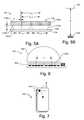
- FIG. 1shows a side view of a device that includes a plurality of light emitting diode (LED) dies mounted on a shared submount and covered by a lens system with a corresponding plurality of lens elements.
- LEDlight emitting diode
- FIG. 2shows a top view of the device of FIG. 1 with the lens system having a plurality of lens elements.
- FIG. 3a side view of a device with a plurality of light emitting diode (LED) dies mounted on a shared submount and covered by a reflective lens system.
- LEDlight emitting diode
- FIG. 4illustrates a perspective view of the fabrication of a device, in accordance with an embodiment of the present invention.
- FIG. 5Ais a side view of a simplified device with a plurality of LED dies mounted on a shared submount and covered by a lens system.
- FIG. 5Bshows the simplified device producing a desired light distribution on a desired target at a predefined distance.
- FIG. 6illustrates another device in which two LED dies are positioned near each other and covered by a single lens.
- FIG. 7illustrates a cell phone with the device from FIG. 1 incorporated therein.
- FIG. 1shows a side view of a device 100 that includes a plurality of light emitting diode (LED) dies 102 a and 102 b mounted on a shared submount 104 that is approximately planar and covered by a lens system 110 .
- FIG. 2shows a top view of the device 100 with the lens system 110 over the LEDs 102 a and 102 b and submount 104 .
- the lens system 110includes a separate lens element 110 a and 110 b that is associated with each of the LED dies 102 a and 102 b .
- the lens elements 110 a and 110 bare separated by a distance that is based on the desired light distribution on target among other optical factors, such as the LED to lens distance, the cone angle of the light for each individual LED, the separation of the LED dies, and the size of the LED dies.
- the LEDs 102 a and 102 b and submount 104can be the type discussed in U.S. Pat. No. 6,885,035, to Bhat, the entirety of which is incorporated herein by reference.
- the p and n contact pads 102 p and 102 nare on the same side of the LEDs 102 a and 102 b , in what is often referred to as a flip-chip or inverted design.
- the light generated by LEDs 102 a and 102 bis coupled out of the LED on the side opposite to the contact pads.
- the LEDs 102 a and 102 bmay be, e.g., the III-nitride type, which has a composition that includes, but is not limited to GaN, AlGaN, AlN, GaInN, AlGaInN, InN, GaInAsN, and GaInPN.
- Typical substrate materialsare sapphire, silicon carbide SiC, or III-nitrides, because of the ease of nucleating and growing high quality III-nitride crystals on these substrates.
- the LEDs 102 a and 102 bmay include a phosphor coating to produce a desired white light.
- the contact pads 102 n and 102 pcan be subsequently electrically connected to metal traces 105 on or in the submount 104 , e.g., by stud bumps 108 .
- the electrical contacts formed by, e.g., the stud bumps 108are between the submount 104 and the bottom surface of the LEDs 102 a and 102 b .
- a self aligning processsuch as a ball grid array (BGA), or other processes, such as thermo-sonic die attachment, may be used to accurately place and attach the LEDs 102 a and 102 b to the submount 104 .
- BGAball grid array
- thermo-sonic die attachmentmay be used to accurately place and attach the LEDs 102 a and 102 b to the submount 104 .
- the accurate placement of the LED diesis advantageous as it permits multiple LED sources to be accurately aligned with a single optical element system 110 with a corresponding number of lens elements 110 a and 110 b .
- the use of BGApermits alignment with a 10 ⁇ m maximum placement error.
- the interconnection between the stud bumps 108 and the metal traces 105 on the submount 104make electrical connection between the LED and the submount while providing a thermal path for heat removal from the LED during operation.
- the interconnectsmay be made of elemental metals, metal alloys, semiconductor-metal alloys, solders, thermally and electrically conductive pastes or compounds (e.g., epoxies), eutectic joints (e.g., Pd—In—Pd) between dissimilar metals between the LED die and submount, or solder bumps.
- elemental metalsmetal alloys, semiconductor-metal alloys, solders, thermally and electrically conductive pastes or compounds (e.g., epoxies), eutectic joints (e.g., Pd—In—Pd) between dissimilar metals between the LED die and submount, or solder bumps.
- the submount 104may be formed from Si or ceramic, such as high-temperature cofired ceramic, or other appropriate materials, such as thin film alumina or other thermal packaging material.
- An optional dielectric layer, e.g. SiO2, (not shown)may be included on the submount for electrical isolation between the LED die and the submount substrate.
- Additional devicesmay be mounted on the submount 104 or within the circuitry 105 on the submount 104 , if desired.
- III-nitride devicesare susceptible to Electro-static Discharge “ESD” damage and may be protected by a power shunting element electrically connected to the LEDs.
- an ESD protection circuit 112may be mounted on the submount 104 . As illustrated in FIG. 1 , the ESD protection circuit 112 may be mounted in the space between the LEDs 102 a and 102 b . If desired, however, the ESD protection circuit 112 may be mounted elsewhere on the submount 104 or off the submount 104 .
- the ESD protection circuit 112may be similar to what is described in Antle et, al. U.S. Pat. No. 5,941,501, which is incorporated herein by reference.
- the ESD protection circuit 112includes Zener diodes connected in parallel with the LEDs 102 a and 102 b .
- back-to-back Zener diodesmay be fabricated in parallel with the LEDs 102 a and 102 b to allow the LED to be driven by alternating-current power supplies.
- Other electronic devicesmay be included on or within the submount, e.g., photodetectors for monitoring light output or resistors for monitoring current and/or voltage.
- the LED dies 102 a and 102 bare separated by a distance X, from center to center.
- the distance Xis sufficiently large that there is room for individual lens element 110 a and 110 b to be formed and positioned over the LED die 102 a and 102 b , respectively.
- the distance Xshould be approximately 130% of the size of the LEDs or greater.
- the individual lens elements 110 a and 110 bare produced so that they are joined together to form a single integral lens system 110 .
- the individual lens elements 110 a and 110 bare substantially flat, such as a refractive Fresnel lens illustrated in FIG. 1 .
- a refractive Fresnel lensillustrated in FIG. 1 .
- other flat lens typesincluding but not limited to a Total Internal Reflection (TIR) Fresnel type lens, a diffractive or a photonic crystal (subwavelength structure) type lens, a prism, reflective lens, or any other optical device that redirects the direction of the light emitted by the LEDs 102 a and 102 b may be used.
- a photonic crystal type lensmay be formed by roughening or texturing a surface of the LED die.
- the textured regionis in the form of a periodic array of holes.
- Photonic crystal structuresare described in more detail in U.S. Pub. No. 2003/0141507 titled “LED efficiency using photonic crystal structure,” which is incorporated herein by reference.
- the periodic array of holeshas a lattice constant, which may range from 0.1 ⁇ to 4 ⁇ , where ⁇ is the wavelength of light emitting by the active region within the semiconductor structure.
- features larger than 2 micronsare formed in the textured region.
- the textured regionacts as a buried light scattering layer within the LED die, which may increase the amount or otherwise affect the light extracted from the device.
- FIG. 3illustrates another type of flat lens system used with a plurality of LED dies.
- a flat reflective lens system 118is positioned over a plurality of LED dies 116 on a submount 118 .
- the lens system 119includes a number of reflective lenses 120 , each reflective lens being associated and aligned with an underlying LED die 116 .
- the lens systemmay be manufactured, e.g., by injection molding, casting, transfer molding, or any other appropriate manner. Where a reflective lens system 119 is used, the lens system 119 may be metalized after forming.
- the device 100may be fabricated by individually coupling the submount 104 with LEDs 102 a and 102 b with the lens system 110 .
- the lens system 110may be bonded to the submount 104 , e.g., using a bonding material, such as a UV or heat cured encapsulant, or snap fitting.
- the lens system 110may be mounted to, bonded, or otherwise formed in the structure of the final application, e.g., in the cell phone body, and the submount 104 with LEDs 102 a and 102 b may be attached to the structure, e.g., using a bonding material or by snap fitting.
- FIG. 4illustrates a perspective view of fabrication of a device 100 , in accordance with another embodiment of the present invention.
- a plurality of submounts 104may be produced simultaneously e.g., in a ceramic wafer form 124 .
- the total wafer 124 sizemay be, e.g., 4 ⁇ 4 inches, while each individual submount 104 may be, e.g., approximately 1 ⁇ 2 mm to 8 ⁇ 12 mm.
- a plurality of lens systems 110may also be produced in an array 128 , e.g., using injection molding, casting, transfer molding, or any other appropriate manner.
- the array 128 of lens systems 110may have a size that is approximately the same size as the submount wafer 124 .
- the submount wafer 124 and array 128 of lens systems 110may be bonded together.
- an encapsulantillustrated as layer 126 , may be used, e.g., by injecting a silicone gel or depositing an encapsulant layer between the lens array 128 and the submount wafer 124 . If desired, the encapsulant 126 need not be used.
- the LED dies 102 a and 102 bmay be covered with or the encapsulant 126 may include a wavelength converting material, such as phosphor, to produce the desired colored light from the finished devices.
- the array 128 and wafer 124can be accurately aligned in the x, y, and z directions using conventional alignment processes. Once aligned, the bonding process can be completed using, e.g., a UV or heat curing. With the array 128 formed from, e.g., a hard silicone, and the encapsulant 126 formed from a soft silicone, the process will be compatible with a lead free solder reflow process. In one embodiment, the alignment in the z-direction can be accomplished using stand off features 129 , which are integrated in the array 128 . The use of one or more stand off features 129 provides a mechanical alignment the underlying submount wafer 124 , but may require the sacrifice of a submount. Once bonded, the wafer 124 and array 128 may be diced into separate devices 100 using conventional dicing techniques.
- FIG. 5Ais a side view of a simplified device 130 with a plurality of LED dies 132 a and 132 b mounted on a shared submount 134 and covered by a lens system 136 having separate lens elements 138 a and 138 b .
- FIG. 5Bshows the device 130 and the desired target 140 , which is a predefined distance D from the device 130 at which the device 130 will produce a desired light distribution on the target 140 .
- the lens elements 138 a and 138 bare separated by a distance X lens , from center to center and the LED dies 132 a and 132 b are separated by a distance X LED .
- the correlation between distances X lens and X LED and the alignment A of the lens system 136 to the underlying LEDs 132 a and 132 bare closely controlled to produce a desired amount of light on the target 140 at distance D.
- the distance X LED between the LED dies 132 a and 132 bmay be, e.g., 130% to 500% or greater of the size of the LED dies, while the distance X lens between lens elements 138 a and 138 b may be approximately 100% to 200% of the distance X LED .
- optical factorssuch as the distance H between the lens elements 138 a , 138 b and the LED dies 132 a , 132 b , the cone angle 133 a , 133 b of the light captured by the lens elements 138 a and 138 b , and the size W 132a , W 132b of the LED dies 132 a , 132 b , also affect amount of light on the target 140 at distance D and, thus, must also be appropriate selected.
- the shape of the resulting cone angle from the light emitted from the device, as well as the direction of the cone with respect to the optical axis of the devicecan be predefined to produce a desired amount of light on target 140 at a desired distance D.
- the accurate placement of the LED dies 132 a and 132 b on the submount 134facilitates control of the correlation between the distances X lens and X LED as well as the alignment A. Moreover, the separation of the LED dies 132 a and 132 b X LED permits the use of a separate lens element 138 a and 138 b for each LED die 132 a and 132 b , respectively. With the use of a separate lens element for each LED die, the efficiency of the system is increased relative to systems that use a single lens for multiple LED dies.
- FIG. 6illustrates a device 150 in which two LED dies 152 a and 152 b (sometimes referred to collectively as LEDs 152 ) are positioned near each other, i.e., the centers are separated by a distance Y, which is less than 30% of the width of the LEDs 152 .
- a distance Ywhich is less than 30% of the width of the LEDs 152 .
- a single lens element 160is used.
- the use of a single lens element 160 with multiple LEDs 152results in a system with reduced efficiency.
- the device 150is much more restricted in the amount of light that can be placed on a target at a predefined distance.
- FIG. 7illustrates a cell phone 200 with a device 100 incorporated therein.
- the device 100 with the separated LEDs 102 and separate lens elements 110 a and 110 bincreases the efficiency of the system by 15% to 45% over a system with a single lens element system and two LEDs.
- the device 100may be incorporated into other applications, where it is desirable to direct the majority of the flux of an LED into a predefined cone angle, such as map lights, reading lights and spotlights.
- the overall designproduces a large amount of illumination from a relatively small device 100 , which is particularly advantageous in applications where there is limited real estate, e.g. in a cell phone flash. Further, the separation of the LEDs 102 a and 102 b is advantageous in heat dissipation, which permits the LEDs 102 a and 102 b to be driven at a slightly increased current.
- LEDs 102 a and 102 badditional LEDs may be used if desired, e.g., 4 ⁇ 4 or 6 ⁇ 6 LED dies, where the LEDs are sufficiently separated to permit a separate lens element for a plurality of the LEDs.
Landscapes
- Engineering & Computer Science (AREA)
- Power Engineering (AREA)
- Microelectronics & Electronic Packaging (AREA)
- Physics & Mathematics (AREA)
- General Physics & Mathematics (AREA)
- Condensed Matter Physics & Semiconductors (AREA)
- Computer Hardware Design (AREA)
- Multimedia (AREA)
- Signal Processing (AREA)
- Led Device Packages (AREA)
- Led Devices (AREA)
Abstract
Description
Claims (25)
Priority Applications (8)
| Application Number | Priority Date | Filing Date | Title |
|---|---|---|---|
| US11/201,465US8163580B2 (en) | 2005-08-10 | 2005-08-10 | Multiple die LED and lens optical system |
| EP06795610.2AEP1915568B1 (en) | 2005-08-10 | 2006-08-08 | Apparatus comprising a plurality of light emitting diode dies and an integral lens system with a plurality of lens elements, and a method of fabricating the same |
| ES06795610TES2719594T3 (en) | 2005-08-10 | 2006-08-08 | Apparatus comprising a plurality of arrays of light emitting diodes and an integral lens system with a plurality of lens elements and a manufacturing method thereof |
| CNA2006800291180ACN101253362A (en) | 2005-08-10 | 2006-08-08 | Light-emitting diodes consisting of multiple dies and an optical system with multiple lens elements |
| PCT/IB2006/052729WO2007017833A1 (en) | 2005-08-10 | 2006-08-08 | Light emitting diode comprising multiple dies and optical system with number of lens elements |
| TW095129240ATWI443855B (en) | 2005-08-10 | 2006-08-09 | Light emitting device and method of manufacturing same |
| JP2006242140AJP5275557B2 (en) | 2005-08-10 | 2006-08-10 | Multiple die LED and lens optical system |
| US13/425,635US8729571B2 (en) | 2005-08-10 | 2012-03-21 | Multiple die LED and lens optical system |
Applications Claiming Priority (1)
| Application Number | Priority Date | Filing Date | Title |
|---|---|---|---|
| US11/201,465US8163580B2 (en) | 2005-08-10 | 2005-08-10 | Multiple die LED and lens optical system |
Related Child Applications (1)
| Application Number | Title | Priority Date | Filing Date |
|---|---|---|---|
| US13/425,635ContinuationUS8729571B2 (en) | 2005-08-10 | 2012-03-21 | Multiple die LED and lens optical system |
Publications (2)
| Publication Number | Publication Date |
|---|---|
| US20070034890A1 US20070034890A1 (en) | 2007-02-15 |
| US8163580B2true US8163580B2 (en) | 2012-04-24 |
Family
ID=37450936
Family Applications (2)
| Application Number | Title | Priority Date | Filing Date |
|---|---|---|---|
| US11/201,465Active2028-03-11US8163580B2 (en) | 2005-08-10 | 2005-08-10 | Multiple die LED and lens optical system |
| US13/425,635Expired - LifetimeUS8729571B2 (en) | 2005-08-10 | 2012-03-21 | Multiple die LED and lens optical system |
Family Applications After (1)
| Application Number | Title | Priority Date | Filing Date |
|---|---|---|---|
| US13/425,635Expired - LifetimeUS8729571B2 (en) | 2005-08-10 | 2012-03-21 | Multiple die LED and lens optical system |
Country Status (7)
| Country | Link |
|---|---|
| US (2) | US8163580B2 (en) |
| EP (1) | EP1915568B1 (en) |
| JP (1) | JP5275557B2 (en) |
| CN (1) | CN101253362A (en) |
| ES (1) | ES2719594T3 (en) |
| TW (1) | TWI443855B (en) |
| WO (1) | WO2007017833A1 (en) |
Cited By (11)
| Publication number | Priority date | Publication date | Assignee | Title |
|---|---|---|---|---|
| US9341341B1 (en)* | 2014-11-21 | 2016-05-17 | Genius Electronic Optical Co., Ltd. | Lens for an illuminating device |
| US9470395B2 (en) | 2013-03-15 | 2016-10-18 | Abl Ip Holding Llc | Optic for a light source |
| US9557028B2 (en) | 2014-11-21 | 2017-01-31 | Genius Electronic Optical Co., Ltd. | Lens for an illuminating device |
| US20170108182A1 (en)* | 2015-10-20 | 2017-04-20 | Panasonic Intellectual Property Management Co., Ltd. | Lighting apparatus |
| WO2018144614A1 (en)* | 2017-02-03 | 2018-08-09 | Apple Inc. | Asymmetric zones in a fresnel lens |
| US20200011504A1 (en)* | 2018-07-04 | 2020-01-09 | Wanjiong Lin | Lighting System |
| US11032976B1 (en) | 2020-03-16 | 2021-06-15 | Hgci, Inc. | Light fixture for indoor grow application and components thereof |
| USD933881S1 (en) | 2020-03-16 | 2021-10-19 | Hgci, Inc. | Light fixture having heat sink |
| USD933872S1 (en) | 2020-03-16 | 2021-10-19 | Hgci, Inc. | Light fixture |
| US11152546B2 (en) | 2017-08-28 | 2021-10-19 | Nichia Corporation | Light-emitting device |
| US12330386B2 (en) | 2013-05-10 | 2025-06-17 | Abl Ip Holding Llc | Silicone optics |
Families Citing this family (75)
| Publication number | Priority date | Publication date | Assignee | Title |
|---|---|---|---|---|
| US9793247B2 (en) | 2005-01-10 | 2017-10-17 | Cree, Inc. | Solid state lighting component |
| US9070850B2 (en) | 2007-10-31 | 2015-06-30 | Cree, Inc. | Light emitting diode package and method for fabricating same |
| US7821023B2 (en)* | 2005-01-10 | 2010-10-26 | Cree, Inc. | Solid state lighting component |
| US7344952B2 (en)* | 2005-10-28 | 2008-03-18 | Philips Lumileds Lighting Company, Llc | Laminating encapsulant film containing phosphor over LEDs |
| US9335006B2 (en) | 2006-04-18 | 2016-05-10 | Cree, Inc. | Saturated yellow phosphor converted LED and blue converted red LED |
| US20090128781A1 (en)* | 2006-06-13 | 2009-05-21 | Kenneth Li | LED multiplexer and recycler and micro-projector incorporating the Same |
| DE102006039705A1 (en)* | 2006-08-18 | 2008-02-28 | Schott Ag | Lens attachment for a headlight |
| US10295147B2 (en) | 2006-11-09 | 2019-05-21 | Cree, Inc. | LED array and method for fabricating same |
| US7702235B2 (en) | 2007-01-25 | 2010-04-20 | Research In Motion Limited | Handheld electronic device and camera providing flash compensation of images, and associated method |
| RU2456503C2 (en)* | 2007-04-05 | 2012-07-20 | Конинклейке Филипс Электроникс Н.В. | Light beam former |
| US20090050921A1 (en)* | 2007-08-23 | 2009-02-26 | Philips Lumileds Lighting Company Llc | Light Emitting Diode Array |
| US7808581B2 (en) | 2008-01-18 | 2010-10-05 | Teledyne Lighting And Display Products, Inc. | Low profile backlight apparatus |
| TW201011349A (en) | 2008-09-10 | 2010-03-16 | E Pin Optical Industry Co Ltd | Plano-Fresnel LED lens for angular distribution patterns and LED assembly thereof |
| TWI364120B (en) | 2008-09-10 | 2012-05-11 | E Pin Optical Industry Co Ltd | Convex-fresnel led lens for angular distribution patterns and led assembly thereof |
| WO2010032224A2 (en)* | 2008-09-22 | 2010-03-25 | Asml Netherlands B.V. | Lithographic apparatus, programmable patterning device and lithographic method |
| US8944626B2 (en) | 2008-10-09 | 2015-02-03 | Surefire, Llc | Lighting device with switchable light sources |
| US8147089B2 (en)* | 2008-10-09 | 2012-04-03 | Surefire, Llc | Switchable light sources |
| US8182109B2 (en)* | 2008-10-09 | 2012-05-22 | Surefire, Llc | Lighting device with switchable light sources |
| US9425172B2 (en) | 2008-10-24 | 2016-08-23 | Cree, Inc. | Light emitter array |
| WO2010048754A1 (en)* | 2008-10-30 | 2010-05-06 | Zhan Xiaoming | Led photography light |
| KR100972983B1 (en)* | 2009-01-09 | 2010-07-29 | 삼성엘이디 주식회사 | Camera flash lens and portable device including the same |
| US8576406B1 (en) | 2009-02-25 | 2013-11-05 | Physical Optics Corporation | Luminaire illumination system and method |
| TWM368029U (en)* | 2009-03-30 | 2009-11-01 | E Pin Internat Tech Co Ltd | Fresnel LED lens and LED assembly thereof |
| US9385285B2 (en)* | 2009-09-17 | 2016-07-05 | Koninklijke Philips N.V. | LED module with high index lens |
| US10005682B1 (en) | 2009-10-02 | 2018-06-26 | Tersano Inc. | Holding tank-less water ozonating system |
| TWI448830B (en) | 2010-02-09 | 2014-08-11 | Asml Netherlands Bv | Lithographic apparatus and device manufacturing method |
| KR101419330B1 (en) | 2010-02-23 | 2014-07-15 | 에이에스엠엘 네델란즈 비.브이. | Lithographic apparatus and device manufacturing method |
| WO2011104172A1 (en) | 2010-02-25 | 2011-09-01 | Asml Netherlands B.V. | Lithographic apparatus and device manufacturing method |
| WO2011128162A1 (en) | 2010-04-12 | 2011-10-20 | Asml Netherlands B.V. | Substrate handling apparatus and lithographic apparatus |
| TWM401210U (en)* | 2010-09-29 | 2011-04-01 | Forward Electronics Co Ltd | Light-emitting diode packaging structure |
| GB2484712A (en)* | 2010-10-21 | 2012-04-25 | Optovate Ltd | Illumination Apparatus |
| JP2014026993A (en)* | 2010-11-08 | 2014-02-06 | Panasonic Corp | Ceramic substrate and light emitting diode module |
| US9316926B2 (en) | 2010-12-08 | 2016-04-19 | Asml Netherlands B.V. | Lithographic apparatus and device manufacturing method |
| US9786811B2 (en) | 2011-02-04 | 2017-10-10 | Cree, Inc. | Tilted emission LED array |
| DE102011003989A1 (en)* | 2011-02-11 | 2012-08-16 | Osram Ag | Lighting device i.e. LED module, has encapsulation chamber encapsulating semiconductor light source, and film-shaped optic element applied on free-surface of encapsulation chamber that consists of casting material such as silicone |
| NL2008329A (en) | 2011-03-29 | 2012-10-02 | Asml Netherlands Bv | Lithographic apparatus, method for measuring radiation beam spot position, device manufacturing method, and radiation detector system for a lithographic apparatus. |
| WO2012136434A2 (en) | 2011-04-08 | 2012-10-11 | Asml Netherlands B.V. | Lithographic apparatus, programmable patterning device and lithographic method |
| NL2008500A (en) | 2011-04-21 | 2012-10-23 | Asml Netherlands Bv | Lithographic apparatus, method for maintaining a lithographic apparatus and device manufacturing method. |
| US8507328B2 (en)* | 2011-05-27 | 2013-08-13 | Tsmc Solid State Lighting Ltd. | Systems and methods providing semiconductor light emitters |
| US10842016B2 (en) | 2011-07-06 | 2020-11-17 | Cree, Inc. | Compact optically efficient solid state light source with integrated thermal management |
| JP5837693B2 (en) | 2011-08-18 | 2015-12-24 | エーエスエムエル ネザーランズ ビー.ブイ. | Lithographic apparatus and device manufacturing method |
| CN102544336A (en)* | 2011-08-20 | 2012-07-04 | 中国科学院福建物质结构研究所 | Visible light full-spectrum high-reflectivity LED (light-emitting diode) packaging structure |
| NL2009342A (en) | 2011-10-31 | 2013-05-07 | Asml Netherlands Bv | Lithographic apparatus and device manufacturing method. |
| US10346729B2 (en) | 2011-11-29 | 2019-07-09 | Asml Netherlands B.V. | Apparatus and method for converting a vector-based representation of a desired device pattern for a lithography apparatus, apparatus and method for providing data to a programmable patterning device, a lithography apparatus and a device manufacturing method |
| KR101616764B1 (en) | 2011-11-29 | 2016-04-29 | 에이에스엠엘 네델란즈 비.브이. | Lithographic apparatus, device manufacturing method and computer program |
| US9341960B2 (en) | 2011-12-05 | 2016-05-17 | Asml Netherlands B.V. | Lithographic apparatus and device manufacturing method |
| WO2013083383A1 (en) | 2011-12-06 | 2013-06-13 | Asml Netherlands B.V. | A lithography apparatus, an apparatus for providing setpoint data, a device manufacturing method, a method of calculating setpoint data and a computer program |
| NL2009902A (en) | 2011-12-27 | 2013-07-01 | Asml Netherlands Bv | Lithographic apparatus and device manufacturing method. |
| JP5916895B2 (en) | 2012-01-12 | 2016-05-11 | エーエスエムエル ネザーランズ ビー.ブイ. | Lithographic apparatus, apparatus for providing setpoint data, device manufacturing method, method for providing setpoint data, and computer program |
| US9568831B2 (en) | 2012-01-17 | 2017-02-14 | Asml Netherlands B.V. | Lithographic apparatus and device manufacturing method |
| DE102012200973A1 (en)* | 2012-01-24 | 2013-07-25 | Osram Opto Semiconductors Gmbh | LIGHT AND METHOD FOR PRODUCING A LIGHT |
| WO2013124114A1 (en) | 2012-02-23 | 2013-08-29 | Asml Netherlands B.V. | Device, lithographic apparatus, method for guiding radiation and device manufacturing method |
| KR101285224B1 (en) | 2012-05-18 | 2013-07-11 | 우리이앤엘 주식회사 | Chip on board type light emitting module |
| NL2012052A (en) | 2013-01-29 | 2014-08-04 | Asml Netherlands Bv | A radiation modulator for a lithography apparatus, a lithography apparatus, a method of modulating radiation for use in lithography, and a device manufacturing method. |
| CN105676322A (en)* | 2014-11-21 | 2016-06-15 | 玉晶光电股份有限公司 | Thin lens |
| CN107533157B (en) | 2015-04-02 | 2019-10-08 | 飞利浦照明控股有限公司 | Light-beam forming unit and the spotlight for using light-beam forming unit |
| US10041646B2 (en) | 2015-05-01 | 2018-08-07 | Cooper Technologies Company | Optic and apparatus for making an optic |
| JP6696129B2 (en)* | 2015-08-28 | 2020-05-20 | 日亜化学工業株式会社 | Light emitting device |
| DE102016101810A1 (en)* | 2016-02-02 | 2017-08-03 | Osram Opto Semiconductors Gmbh | LIGHT DEVICE |
| CN105650599A (en)* | 2016-03-30 | 2016-06-08 | 宁波正特光学电器有限公司 | Lens for mobile phone flashlight module |
| US10663745B2 (en) | 2016-06-09 | 2020-05-26 | 3M Innovative Properties Company | Optical system |
| US10420177B2 (en) | 2016-12-19 | 2019-09-17 | Whelen Engineering Company, Inc. | LED illumination module with fixed optic and variable emission pattern |
| US10400994B2 (en) | 2016-12-19 | 2019-09-03 | Whelen Engineering Company, Inc. | LED illumination module with fixed optic and variable emission pattern |
| US10582169B2 (en)* | 2016-12-23 | 2020-03-03 | Lumileds Llc | Compensating for vignetting |
| WO2019061065A1 (en)* | 2017-09-27 | 2019-04-04 | 深圳传音制造有限公司 | Flash lamp structure and terminal having same |
| JP7132502B2 (en) | 2018-03-09 | 2022-09-07 | 日亜化学工業株式会社 | Light source device |
| US10770632B2 (en) | 2018-03-09 | 2020-09-08 | Nichia Corporation | Light source device |
| JP6912732B2 (en) | 2018-08-31 | 2021-08-04 | 日亜化学工業株式会社 | Light emitting device and its manufacturing method |
| US12436291B2 (en) | 2019-03-19 | 2025-10-07 | Sony Semiconductor Solutions Corporation | Sensor chip, electronic apparatus, and distance measurement apparatus |
| JP6951644B2 (en)* | 2019-04-23 | 2021-10-20 | 日亜化学工業株式会社 | Light emitting module and its manufacturing method |
| JP7636657B2 (en) | 2020-01-23 | 2025-02-27 | 日亜化学工業株式会社 | Light source |
| JP7545032B2 (en) | 2020-01-23 | 2024-09-04 | 日亜化学工業株式会社 | Light source |
| WO2021210246A1 (en)* | 2020-04-15 | 2021-10-21 | 株式会社ジャパンディスプレイ | Prism sheet and illumination device using same |
| CN111580327A (en)* | 2020-05-08 | 2020-08-25 | Oppo(重庆)智能科技有限公司 | Flash lamp module, electronic equipment and control method thereof |
| US12284846B2 (en)* | 2021-06-07 | 2025-04-22 | Lumileds Llc | Light-emitting device with internal non-specular light redirection and position-dependent reflection, transmission, or redirection |
Citations (19)
| Publication number | Priority date | Publication date | Assignee | Title |
|---|---|---|---|---|
| WO1989005524A1 (en) | 1987-11-30 | 1989-06-15 | Iwasaki Electric Co., Ltd | Planar led illuminant |
| EP0424175A2 (en) | 1989-10-20 | 1991-04-24 | Minnesota Mining And Manufacturing Company | Production of grey scale images using pixellated exposure devices |
| US5914501A (en) | 1998-08-27 | 1999-06-22 | Hewlett-Packard Company | Light emitting diode assembly having integrated electrostatic discharge protection |
| US5995071A (en)* | 1997-11-21 | 1999-11-30 | Hewlett-Packard Company | Reflective display utilizing fresnel micro-reflectors |
| US20010048814A1 (en)* | 2000-05-26 | 2001-12-06 | Mathias Lenmann | Photographic Image acquisition device using LED chips |
| WO2002056361A1 (en) | 2001-01-10 | 2002-07-18 | Silverbrook Research Pty. Ltd. | Light emitting semiconductor package |
| WO2003023857A2 (en) | 2001-09-13 | 2003-03-20 | Lucea Ag | Led-luminous panel and carrier plate |
| US6570324B1 (en) | 2000-07-19 | 2003-05-27 | Eastman Kodak Company | Image display device with array of lens-lets |
| US6583444B2 (en)* | 1997-02-18 | 2003-06-24 | Tessera, Inc. | Semiconductor packages having light-sensitive chips |
| US20030141507A1 (en) | 2002-01-28 | 2003-07-31 | Krames Michael R. | LED efficiency using photonic crystal structure |
| WO2004070839A2 (en) | 2003-02-05 | 2004-08-19 | Acol Technologies S.A. | Light emitting apparatus comprising semiconductor light emitting devices |
| WO2005034198A2 (en) | 2003-10-01 | 2005-04-14 | Enertron, Inc. | Methods and apparatus for an led light engine |
| US6885035B2 (en)* | 1999-12-22 | 2005-04-26 | Lumileds Lighting U.S., Llc | Multi-chip semiconductor LED assembly |
| US20050104073A1 (en) | 2003-11-18 | 2005-05-19 | Shen-Hong Chou | Solid-state display with improved color-mixing |
| EP1564819A1 (en) | 2002-11-05 | 2005-08-17 | Matsushita Electric Industrial Co., Ltd. | Light-emitting diode |
| WO2005091386A1 (en) | 2004-03-24 | 2005-09-29 | Toshiba Lighting & Technology Corporation | Lighting system |
| US6987613B2 (en)* | 2001-03-30 | 2006-01-17 | Lumileds Lighting U.S., Llc | Forming an optical element on the surface of a light emitting device for improved light extraction |
| US20060139953A1 (en)* | 2004-12-24 | 2006-06-29 | Prodisc Technology Inc. | Liquid crystal display and backlight module thereof |
| US20110057205A1 (en)* | 2004-11-15 | 2011-03-10 | Koninklijke Philips Electronics N.V. | Led with phosphor tile and overmolded phosphor in lens |
Family Cites Families (7)
| Publication number | Priority date | Publication date | Assignee | Title |
|---|---|---|---|---|
| JP2518236B2 (en)* | 1986-12-19 | 1996-07-24 | オムロン株式会社 | Light source |
| WO2003065464A1 (en) | 2002-01-28 | 2003-08-07 | Nichia Corporation | Nitride semiconductor device having support substrate and its manufacturing method |
| US7528421B2 (en)* | 2003-05-05 | 2009-05-05 | Lamina Lighting, Inc. | Surface mountable light emitting diode assemblies packaged for high temperature operation |
| JP4360127B2 (en)* | 2003-06-02 | 2009-11-11 | 株式会社小糸製作所 | Vehicle lighting |
| JP4437675B2 (en)* | 2003-12-26 | 2010-03-24 | 日本精機株式会社 | Lighting device |
| US20060044806A1 (en)* | 2004-08-25 | 2006-03-02 | Abramov Vladimir S | Light emitting diode system packages |
| JP2007042901A (en)* | 2005-08-04 | 2007-02-15 | Rohm Co Ltd | Light emitting module and light emitting unit |
- 2005
- 2005-08-10USUS11/201,465patent/US8163580B2/enactiveActive
- 2006
- 2006-08-08CNCNA2006800291180Apatent/CN101253362A/enactivePending
- 2006-08-08ESES06795610Tpatent/ES2719594T3/enactiveActive
- 2006-08-08EPEP06795610.2Apatent/EP1915568B1/enactiveActive
- 2006-08-08WOPCT/IB2006/052729patent/WO2007017833A1/enactiveApplication Filing
- 2006-08-09TWTW095129240Apatent/TWI443855B/enactive
- 2006-08-10JPJP2006242140Apatent/JP5275557B2/enactiveActive
- 2012
- 2012-03-21USUS13/425,635patent/US8729571B2/ennot_activeExpired - Lifetime
Patent Citations (19)
| Publication number | Priority date | Publication date | Assignee | Title |
|---|---|---|---|---|
| WO1989005524A1 (en) | 1987-11-30 | 1989-06-15 | Iwasaki Electric Co., Ltd | Planar led illuminant |
| EP0424175A2 (en) | 1989-10-20 | 1991-04-24 | Minnesota Mining And Manufacturing Company | Production of grey scale images using pixellated exposure devices |
| US6583444B2 (en)* | 1997-02-18 | 2003-06-24 | Tessera, Inc. | Semiconductor packages having light-sensitive chips |
| US5995071A (en)* | 1997-11-21 | 1999-11-30 | Hewlett-Packard Company | Reflective display utilizing fresnel micro-reflectors |
| US5914501A (en) | 1998-08-27 | 1999-06-22 | Hewlett-Packard Company | Light emitting diode assembly having integrated electrostatic discharge protection |
| US6885035B2 (en)* | 1999-12-22 | 2005-04-26 | Lumileds Lighting U.S., Llc | Multi-chip semiconductor LED assembly |
| US20010048814A1 (en)* | 2000-05-26 | 2001-12-06 | Mathias Lenmann | Photographic Image acquisition device using LED chips |
| US6570324B1 (en) | 2000-07-19 | 2003-05-27 | Eastman Kodak Company | Image display device with array of lens-lets |
| WO2002056361A1 (en) | 2001-01-10 | 2002-07-18 | Silverbrook Research Pty. Ltd. | Light emitting semiconductor package |
| US6987613B2 (en)* | 2001-03-30 | 2006-01-17 | Lumileds Lighting U.S., Llc | Forming an optical element on the surface of a light emitting device for improved light extraction |
| WO2003023857A2 (en) | 2001-09-13 | 2003-03-20 | Lucea Ag | Led-luminous panel and carrier plate |
| US20030141507A1 (en) | 2002-01-28 | 2003-07-31 | Krames Michael R. | LED efficiency using photonic crystal structure |
| EP1564819A1 (en) | 2002-11-05 | 2005-08-17 | Matsushita Electric Industrial Co., Ltd. | Light-emitting diode |
| WO2004070839A2 (en) | 2003-02-05 | 2004-08-19 | Acol Technologies S.A. | Light emitting apparatus comprising semiconductor light emitting devices |
| WO2005034198A2 (en) | 2003-10-01 | 2005-04-14 | Enertron, Inc. | Methods and apparatus for an led light engine |
| US20050104073A1 (en) | 2003-11-18 | 2005-05-19 | Shen-Hong Chou | Solid-state display with improved color-mixing |
| WO2005091386A1 (en) | 2004-03-24 | 2005-09-29 | Toshiba Lighting & Technology Corporation | Lighting system |
| US20110057205A1 (en)* | 2004-11-15 | 2011-03-10 | Koninklijke Philips Electronics N.V. | Led with phosphor tile and overmolded phosphor in lens |
| US20060139953A1 (en)* | 2004-12-24 | 2006-06-29 | Prodisc Technology Inc. | Liquid crystal display and backlight module thereof |
Cited By (18)
| Publication number | Priority date | Publication date | Assignee | Title |
|---|---|---|---|---|
| US10578276B2 (en) | 2013-03-15 | 2020-03-03 | Abl Ip Holding Llc | Optic for a light source |
| US9470395B2 (en) | 2013-03-15 | 2016-10-18 | Abl Ip Holding Llc | Optic for a light source |
| US10890313B2 (en) | 2013-03-15 | 2021-01-12 | Abl Ip Holding Llc | Optic for a light source |
| US12330386B2 (en) | 2013-05-10 | 2025-06-17 | Abl Ip Holding Llc | Silicone optics |
| US9557028B2 (en) | 2014-11-21 | 2017-01-31 | Genius Electronic Optical Co., Ltd. | Lens for an illuminating device |
| US9341341B1 (en)* | 2014-11-21 | 2016-05-17 | Genius Electronic Optical Co., Ltd. | Lens for an illuminating device |
| US20170108182A1 (en)* | 2015-10-20 | 2017-04-20 | Panasonic Intellectual Property Management Co., Ltd. | Lighting apparatus |
| US10151431B2 (en)* | 2015-10-20 | 2018-12-11 | Panasonic Intellectual Property Management Co., Ltd. | Lighting apparatus with lens having safety light-dispersing structures |
| WO2018144614A1 (en)* | 2017-02-03 | 2018-08-09 | Apple Inc. | Asymmetric zones in a fresnel lens |
| US10578949B2 (en) | 2017-02-03 | 2020-03-03 | Apple Inc. | Asymmetric zones in a Fresnel lens |
| US11467472B2 (en) | 2017-02-03 | 2022-10-11 | Apple Inc. | Asymmetric zones in a fresnel lens |
| US11152546B2 (en) | 2017-08-28 | 2021-10-19 | Nichia Corporation | Light-emitting device |
| US11710810B2 (en) | 2017-08-28 | 2023-07-25 | Nichia Corporation | Light-emitting device |
| US12295189B2 (en) | 2017-08-28 | 2025-05-06 | Nichia Corporation | Light-emitting device |
| US20200011504A1 (en)* | 2018-07-04 | 2020-01-09 | Wanjiong Lin | Lighting System |
| US11032976B1 (en) | 2020-03-16 | 2021-06-15 | Hgci, Inc. | Light fixture for indoor grow application and components thereof |
| USD933881S1 (en) | 2020-03-16 | 2021-10-19 | Hgci, Inc. | Light fixture having heat sink |
| USD933872S1 (en) | 2020-03-16 | 2021-10-19 | Hgci, Inc. | Light fixture |
Also Published As
| Publication number | Publication date |
|---|---|
| WO2007017833A1 (en) | 2007-02-15 |
| JP2007049172A (en) | 2007-02-22 |
| TWI443855B (en) | 2014-07-01 |
| CN101253362A (en) | 2008-08-27 |
| US20070034890A1 (en) | 2007-02-15 |
| US20130069084A1 (en) | 2013-03-21 |
| JP5275557B2 (en) | 2013-08-28 |
| EP1915568B1 (en) | 2019-02-27 |
| ES2719594T3 (en) | 2019-07-11 |
| TW200711186A (en) | 2007-03-16 |
| US8729571B2 (en) | 2014-05-20 |
| EP1915568A1 (en) | 2008-04-30 |
Similar Documents
| Publication | Publication Date | Title |
|---|---|---|
| US8163580B2 (en) | Multiple die LED and lens optical system | |
| US8445928B2 (en) | Light-emitting diode light source module | |
| US10295147B2 (en) | LED array and method for fabricating same | |
| TWI459581B (en) | Sub-substrate for semiconductor light-emitting device package and semiconductor light-emitting device package including the same | |
| CN101971343B (en) | Photoelectric components | |
| US10249798B2 (en) | Light emitting device | |
| US7461948B2 (en) | Multiple light emitting diodes with different secondary optics | |
| TWI422044B (en) | Wafer-scale method for packaging light-emitting device and light-emitting device packaged by wafer scale | |
| US7646035B2 (en) | Packaged light emitting devices including multiple index lenses and multiple index lenses for packaged light emitting devices | |
| US6614172B2 (en) | High efficiency white light emitting diode | |
| US8231251B2 (en) | Multiple piece reflective angle transformer | |
| US8003998B2 (en) | Light-emitting diode arrangement | |
| KR100610650B1 (en) | LED package and manufacturing method | |
| TW201234678A (en) | Multi-chip LED devices | |
| TWI751578B (en) | Flash modules and method for producing flash modules | |
| TW202112181A (en) | Integrated light-emitting device, and light-emitting module | |
| KR20140106652A (en) | Light-emitting diode arrangement | |
| KR20140134420A (en) | Method for manufacturing semiconductor light emitting device package | |
| KR101087854B1 (en) | Semiconductor light emitting device |
Legal Events
| Date | Code | Title | Description |
|---|---|---|---|
| AS | Assignment | Owner name:LUMILEDS LIGHTING U.S., LLC, CALIFORNIA Free format text:ASSIGNMENT OF ASSIGNORS INTEREST;ASSIGNORS:DASCHNER, WALTER;QUAN, XINA;WANG, NANZE P.;SIGNING DATES FROM 20050728 TO 20050802;REEL/FRAME:016886/0531 Owner name:LUMILEDS LIGHTING U.S., LLC, CALIFORNIA Free format text:ASSIGNMENT OF ASSIGNORS INTEREST;ASSIGNORS:DASCHNER, WALTER;QUAN, XINA;WANG, NANZE P.;REEL/FRAME:016886/0531;SIGNING DATES FROM 20050728 TO 20050802 | |
| AS | Assignment | Owner name:PHILIPS LUMILEDS LIGHTING COMPANY LLC, CALIFORNIA Free format text:CHANGE OF NAME;ASSIGNORS:LUMILEDS LIGHTING U.S., LLC;LUMILEDS LIGHTING, U.S., LLC;LUMILEDS LIGHTING, U.S. LLC;AND OTHERS;REEL/FRAME:025850/0770 Effective date:20110211 | |
| STCF | Information on status: patent grant | Free format text:PATENTED CASE | |
| FPAY | Fee payment | Year of fee payment:4 | |
| AS | Assignment | Owner name:DEUTSCHE BANK AG NEW YORK BRANCH, AS COLLATERAL AGENT, NEW YORK Free format text:SECURITY INTEREST;ASSIGNOR:LUMILEDS LLC;REEL/FRAME:043108/0001 Effective date:20170630 Owner name:DEUTSCHE BANK AG NEW YORK BRANCH, AS COLLATERAL AG Free format text:SECURITY INTEREST;ASSIGNOR:LUMILEDS LLC;REEL/FRAME:043108/0001 Effective date:20170630 | |
| AS | Assignment | Owner name:LUMILEDS LLC, CALIFORNIA Free format text:CHANGE OF NAME;ASSIGNOR:PHILIPS LUMILEDS LIGHTING COMPANY, LLC;REEL/FRAME:046111/0261 Effective date:20150326 | |
| MAFP | Maintenance fee payment | Free format text:PAYMENT OF MAINTENANCE FEE, 8TH YEAR, LARGE ENTITY (ORIGINAL EVENT CODE: M1552); ENTITY STATUS OF PATENT OWNER: LARGE ENTITY Year of fee payment:8 | |
| AS | Assignment | Owner name:SOUND POINT AGENCY LLC, NEW YORK Free format text:SECURITY INTEREST;ASSIGNORS:LUMILEDS LLC;LUMILEDS HOLDING B.V.;REEL/FRAME:062299/0338 Effective date:20221230 | |
| MAFP | Maintenance fee payment | Free format text:PAYMENT OF MAINTENANCE FEE, 12TH YEAR, LARGE ENTITY (ORIGINAL EVENT CODE: M1553); ENTITY STATUS OF PATENT OWNER: LARGE ENTITY Year of fee payment:12 | |
| AS | Assignment | Owner name:LUMILEDS HOLDING B.V., NETHERLANDS Free format text:RELEASE BY SECURED PARTY;ASSIGNOR:SOUND POINT AGENCY LLC;REEL/FRAME:070046/0001 Effective date:20240731 Owner name:LUMILEDS LLC, CALIFORNIA Free format text:RELEASE BY SECURED PARTY;ASSIGNOR:SOUND POINT AGENCY LLC;REEL/FRAME:070046/0001 Effective date:20240731 | |
| AS | Assignment | Owner name:LUMILEDS SINGAPORE PTE. LTD., SINGAPORE Free format text:ASSIGNMENT OF ASSIGNORS INTEREST;ASSIGNOR:LUMILEDS LLC;REEL/FRAME:071888/0086 Effective date:20250708 |