US8161348B2 - Systems and methods for low cost LDPC decoding - Google Patents
Systems and methods for low cost LDPC decodingDownload PDFInfo
- Publication number
- US8161348B2 US8161348B2US12/025,924US2592408AUS8161348B2US 8161348 B2US8161348 B2US 8161348B2US 2592408 AUS2592408 AUS 2592408AUS 8161348 B2US8161348 B2US 8161348B2
- Authority
- US
- United States
- Prior art keywords
- update
- perform
- column
- soft
- arithmetic unit
- Prior art date
- Legal status (The legal status is an assumption and is not a legal conclusion. Google has not performed a legal analysis and makes no representation as to the accuracy of the status listed.)
- Active, expires
Links
- 238000000034methodMethods0.000titleclaimsdescription34
- 230000015654memoryEffects0.000claimsabstractdescription83
- 230000006870functionEffects0.000claimsdescription44
- 230000009977dual effectEffects0.000claimsdescription19
- 230000005540biological transmissionEffects0.000claimsdescription3
- 239000011159matrix materialSubstances0.000description31
- 230000008569processEffects0.000description8
- 238000013461designMethods0.000description6
- 238000012545processingMethods0.000description4
- 238000010586diagramMethods0.000description3
- 230000005291magnetic effectEffects0.000description2
- 238000013500data storageMethods0.000description1
- 230000002708enhancing effectEffects0.000description1
- 238000013507mappingMethods0.000description1
- 238000012986modificationMethods0.000description1
- 230000004048modificationEffects0.000description1
- 230000009467reductionEffects0.000description1
Images


Classifications
- H—ELECTRICITY
- H03—ELECTRONIC CIRCUITRY
- H03M—CODING; DECODING; CODE CONVERSION IN GENERAL
- H03M13/00—Coding, decoding or code conversion, for error detection or error correction; Coding theory basic assumptions; Coding bounds; Error probability evaluation methods; Channel models; Simulation or testing of codes
- H03M13/03—Error detection or forward error correction by redundancy in data representation, i.e. code words containing more digits than the source words
- H03M13/05—Error detection or forward error correction by redundancy in data representation, i.e. code words containing more digits than the source words using block codes, i.e. a predetermined number of check bits joined to a predetermined number of information bits
- H03M13/11—Error detection or forward error correction by redundancy in data representation, i.e. code words containing more digits than the source words using block codes, i.e. a predetermined number of check bits joined to a predetermined number of information bits using multiple parity bits
- H03M13/1102—Codes on graphs and decoding on graphs, e.g. low-density parity check [LDPC] codes
- H03M13/1105—Decoding
- H03M13/1131—Scheduling of bit node or check node processing
- H03M13/1137—Partly parallel processing, i.e. sub-blocks or sub-groups of nodes being processed in parallel
- H—ELECTRICITY
- H03—ELECTRONIC CIRCUITRY
- H03M—CODING; DECODING; CODE CONVERSION IN GENERAL
- H03M13/00—Coding, decoding or code conversion, for error detection or error correction; Coding theory basic assumptions; Coding bounds; Error probability evaluation methods; Channel models; Simulation or testing of codes
- H03M13/03—Error detection or forward error correction by redundancy in data representation, i.e. code words containing more digits than the source words
- H03M13/05—Error detection or forward error correction by redundancy in data representation, i.e. code words containing more digits than the source words using block codes, i.e. a predetermined number of check bits joined to a predetermined number of information bits
- H03M13/11—Error detection or forward error correction by redundancy in data representation, i.e. code words containing more digits than the source words using block codes, i.e. a predetermined number of check bits joined to a predetermined number of information bits using multiple parity bits
- H03M13/1102—Codes on graphs and decoding on graphs, e.g. low-density parity check [LDPC] codes
- H03M13/1105—Decoding
- H03M13/1111—Soft-decision decoding, e.g. by means of message passing or belief propagation algorithms
- H—ELECTRICITY
- H03—ELECTRONIC CIRCUITRY
- H03M—CODING; DECODING; CODE CONVERSION IN GENERAL
- H03M13/00—Coding, decoding or code conversion, for error detection or error correction; Coding theory basic assumptions; Coding bounds; Error probability evaluation methods; Channel models; Simulation or testing of codes
- H03M13/63—Joint error correction and other techniques
- H03M13/6325—Error control coding in combination with demodulation
Definitions
- the present inventionis related to systems and methods for decoding information, and more particularly to systems and methods for LDPC decoding using the sum product.
- LDPClow-density parity-check
- FIG. 1an exemplary prior art check-to-bit circuit (i.e., a row update circuit) 100 is depicted.
- the parity check matrixhas columns of weight four and rows of weight thirty-six, and includes a total of 18,432 nonzero entries.
- the parity check informationis also commonly represented in a bi-partite graph as five hundred, twelve (512) check nodes and four thousand, six hundred and eight (4608) bit nodes.
- the architectureincludes two distinct look up tables 110 , 112 and two distinct FIFO memories 120 , 122 that are used to implement a sum product algorithm.
- the architecture of check-to-bit circuit 100uses both look up tables 110 , 112 at the same time during a row update. Such an architecture provides reasonable decode results, however, it is expensive in terms of circuitry and die area.
- the present inventionis related to systems and methods for decoding information, and more particularly to systems and methods for LDPC decoding using the sum product.
- Some embodiments of the present inventionprovide LDPC decoders that include arithmetic units with a reconfigurable hardware circuit.
- the reconfigurable hardware circuitis selectably operable to perform a row update, a column update and a load/unload function.
- the LDPC decoderfurther includes a memory unit communicably coupled to the arithmetic unit.
- the load/unload functionis operable to simultaneously load soft inputs to a memory unit, and to unload soft outputs from the memory unit.
- the memory unitincludes a dual port RAM, a counter and an address look-up table. In such instances, the dual port RAM is addressed directly from the counter during a column update and indirectly by applying an output from the counter to the address look-up table during a row update.
- the LDPC decoderfurther includes a soft-input memory communicably coupled to the arithmetic unit.
- the LDPC decoderis operable to receive a set of soft-inputs to both the soft-input memory and the arithmetic unit in parallel.
- the soft-input memoryis a FIFO.
- the arithmetic unitincludes a set of look-up tables. This same look-up table is used to perform both the row update function and the column update function.
- Other embodiments of the present inventionprovide methods for performing LDPC decoding. Such methods include providing an LDPC decoder that has an arithmetic unit, a soft-input memory, and a memory unit. The methods further include configuring the arithmetic unit to perform a row update and performing the row update, and configuring the arithmetic unit to perform a column update and performing the column update. In such cases, a substantial portion of the hardware used to perform the row update is re-used to perform the column update. In some particular cases, over one half of the circuitry used to perform the row update is re-used to perform the column update. In more particular cases, more than ninety-percent of the circuitry used to perform the row update is re-used to perform the column update. In one particular case, approximately all of the circuitry used to perform the row update is re-used to perform the column update.
- the methodsfurther include configuring the arithmetic unit to perform a load/unload function.
- the arithmetic unitto perform a load/unload function.
- at least some of the circuitry used to perform the row updateis re-used to perform the load/unload function.
- a substantial portion of the circuitry used to perform the row updateis re-used to perform the load/unload function.
- perform the load/unload functionincludes simultaneously loading soft-inputs into the memory unit and unloading soft-outputs from the memory unit.
- the memory unitincludes a dual port RAM.
- performing a row updateincludes reading information from the memory unit using a counter to directly address the dual port RAM.
- the memory unitfurther includes an address look-up table.
- performing a column updateincludes reading information from the memory unit using a counter to indirectly address the dual port RAM via the address look-up table.
- configuring the arithmetic unit to perform the row updateincludes selectably asserting inputs to one or more multiplexers of a reconfigurable hardware circuit.
- Configuring the arithmetic unit to perform the column updateincludes selectably asserting inputs to one or more multiplexers of a reconfigurable hardware circuit.
- the arithmetic unitincludes a look-up table. In such instances, configuring the arithmetic unit to perform a row update and configuring the arithmetic unit to perform a column update result in using the same look-up table for both the column update and the row update.
- decoder circuitsthat include a soft-input memory, a memory unit, and an arithmetic unit.
- the arithmetic unitincludes a hardware circuit that is selectably operable to perform a row update and a column update. In such cases, a substantial portion of the circuitry of the hardware circuit used to perform the row update is re-used to perform the column update. In some cases, at least half of the circuitry of the hardware circuit used to perform the row update is re-used to perform the column update.
- the hardware circuitis further selectably operable to perform a load/unload function. In such cases, the load/unload function includes a simultaneous loading of soft-inputs into the memory unit and unloading soft-outputs from the memory unit.
- FIG. 1depicts a prior art check-to-bit (i.e., row update) circuit
- FIG. 2depicts an LDPC decoder in accordance with some embodiments of the present invention
- FIG. 3is a flow diagram depicting operation of an LDPC decoder in accordance with some embodiments of the present invention.
- FIG. 4shows a reconfigurable hardware set that provides for row update, column update, and load/unload functionality in accordance with some embodiments of the present invention
- FIG. 5depicts the reconfigurable hardware of FIG. 4 configured to perform a row update in accordance with various embodiments of the present invention
- FIG. 6depicts the reconfigurable hardware of FIG. 4 configured to perform a column update in accordance with one or more embodiments of the present invention
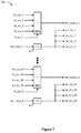
- FIG. 7depicts the reconfigurable hardware of FIG. 4 configured to perform a load/unload function in accordance with various embodiments of the present invention.
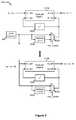
- FIG. 8depicts a dual port memory design that may be used in relation to different embodiments of the present invention.
- the present inventionis related to systems and methods for decoding information, and more particularly to systems and methods for LDPC decoding using the sum product.
- an LDCP decoder 200in accordance with one or more embodiments of the present invention is depicted.
- a sum product algorithmis implemented where an arithmetic unit 210 is configurable to be shared between a row update function and a column update function.
- Such sharingresults in a reduction in circuitry and die area including, but not limited to, utilization of fifty percent fewer look up tables when compared with other prior art LDPC decoders.
- LDCP decoder 200uses only a single look up table compared to the two look up tables prescribed in Yeo et al., “VLSI Architectures for Iterative Decoders in Magnetic Recording Channels”, IEEE Transactions on Magnetics, Vol. 37, March 2001. The entirety of the aforementioned reference is incorporated herein by reference for all purposes.
- a memory unit 220 of LDCP decoder 200is shared between row and column update circuitry.
- memory unit 220stores only ‘w’ messages, where w is the number of 1s of the parity check matrix.
- LDPC decoder 200provides for writing soft-input values 240 into a soft-input memory 230 at the same time that soft-outputs 250 of the previously decoded codeword are provided.
- Soft-input memory 230may be implemented as a simple buffer or FIFO that stores the prescribed number of soft-inputs. Alternatively, it may be implemented using a single-port RAM whose width is a number of times that of the bit-width of the soft-inputs.
- soft-input memory 230is always accessed in the same order (i.e. address 1, address 2, address 3, . . . address n). In such cases, soft-input memory 230 does not need the full random access flexibility of a RAM, and thus may be implemented by SAMs (sequential access memories) which require less area and power than RAMs.
- the parity check matrices supported by LDPC decoder 200are defined by the following parameters:
- Such LDPC decoderscan support LDPC codes whose parity check matrix is decomposed into nine 512 ⁇ 512 sub-matrices with each sub-matrix having a row weight of four and a column weight of four (i.e., 36/9).
- the parity check matrixmay be composed by interleaving the columns of the nine sub-matrices such that the first nine columns of the parity check matrix are equivalent to the first column of each of the respective sub-matrices as follows:
- the 512 ⁇ 512 sub-matricesmay have a column weight of four and row weight of four.
- Such codescan be mapped onto the proposed architecture by simple column permutation (i.e. interleaving) of the parity check matrix.
- locations of the 1s of the four matrices H i,1 , H i,2 , H i,3 , H i,4are non-overlapping.
- thirty-six 512 ⁇ 512 matrices(i.e., 9*4) each with a column weight of one and row weight of one.
- Each of these thirty-six matricesmay be mapped onto a single memory as more dully discussed below.
- a flow diagram 300depicts operation of an LDPC decoder in accordance with some embodiments of the present invention.
- an initial set of soft input valuesare loaded into soft-input memory 230 and to arithmetic unit 210 (block 305 ).
- the number of soft-inputs that are loadedis four thousand, six hundred, eight (4608).
- nine soft inputsare processed by arithmetic unit 210 during each clock cycle resulting in thirty-six messages that are stored back to memory unit 220 .
- five hundred, twelve clock cyclesare required to load the 4608 soft-inputs at nine per clock cycle.
- the hardware of the LDPC decoderis configured to perform a row update (block 315 ), and the row update is performed (block 320 ).
- Various embodiments of the present inventionreuse common circuitry to perform row updates, column updates and load/unload functions.
- Configuring the hardware to perform a row updateincludes selectably configuring the hardware such that it is tailored to perform a row update.
- memory unit 220sends the messages of one entire row (e.g., from the example above this would be thirty-six messages) to arithmetic unit 210 , which updates these messages and returns them to memory unit 220 .
- ⁇ ( x )⁇ log(tan h ( x/ 2)).
- the hardware of the LDPC decoderis re-configured to perform a column update (block 325 ) and the column update is performed (block 330 ).
- Configuring the hardware to perform a column updateincludes selectably configuring the hardware such that it is tailored to perform a column update.
- memory unit 220sends the messages of a number of columns (e.g., in the example messages associated with nine columns are sent) to arithmetic unit 210 , which updates these messages and returns them to memory unit 220 . Simultaneously, for each clock cycle, the soft-input memory sends nine soft-input values (i.e., L input,i ) to arithmetic unit 210 .
- arithmetic unit 210generates soft-output values that are forwarded as the output of the LDPC decoder. This is caused by re-configuring the hardware of the LDPC decoder to perform a simultaneous unload and load function (block 350 ). Each of the aforementioned soft-output values are provided from arithmetic unit 210 as soft-outputs as set forth in the following equation:
- each iteration of the LDPC decoderi.e., blocks 315 - 345
- each iteration of the LDPC decoderis completed in one thousand, twenty-four (1024) clock cycles.
- the loading and unloading processesare completed in parallel with the processing of the last column update, no additional clock cycles are required for loading and unloading.
- arithmetic unit 210is capable of being reconfigured to perform the various functions demanded of the LDPC decoder.
- arithmetic unit 210is capable being reconfigured to performing a row update, a column update and a load and unload function.
- FIG. 4a reconfigurable hardware set 400 is shown that may be selectably re-configured to perform the aforementioned functions in accordance with some embodiments of the present invention.
- Reconfigurable hardware set 400includes a number of parallel circuits 410 .
- One particular embodiment of the present inventionincludes nine parallel circuits 410 corresponding to the number of soft-inputs processed on a given clock cycle.
- Each parallel circuit 410includes a set of look-up tables 417 that is shared across parallel circuits 410 , and a number of multi-input arithmetic function units 421 , 422 , 423 , 424 , 425 .
- the configuration of the aforementioned look up table and arithmetic function unitsis controlled by selection of a number of multiplexers 411 , 412 , 413 , 414 , 416 .
- multiplexers 411 , 412 , 413 , 414 , 416allows for configuring reconfigurable hardware set 400 to implement the following equation for loading corresponding to block 305 discussed above in relation to FIG. 3 :
- ⁇ (
- ) sgn ( m j,i )sgn ( L input,i )
- selection of multiplexers 411 , 412 , 413 , 414 , 416allows for configuring reconfigurable hardware set 400 to implement the following equation for row updates corresponding to blocks 315 - 320 discussed above in relation to FIG. 3 :
- the set of look-up tablesmay be either implemented by synthesized combinational logic or by a ROM depending upon particular design constraints.
- storing ⁇ (x)takes the same amount of memory bits as storing x would take.
- arithmetic unit 210exploits this fact to reduce the number of required look-up tables by using the preceding equations.
- messagesare stored to memory unit 220 in sign-magnitude representation.
- the messages from memory unit 220 to arithmetic unit 210are designated by the notation mu_au_x, where x is a number from one to the total messages.
- the messages from arithmetic unit 210 to memory unit 220are designated by the notation au_mu_y, where y is a number from one to the total messages.
- the soft-inputsare designated by the notation soft_input z, where z is a number between one and the total number of soft-inputs per clock cycle.
- inputs from soft-input memory 230are designated as im_au_w, where w is a number between 1 and the total number of inputs form soft-input memory 230 for a given clock cycle.
- multiplexers 411 , 412 , 413 , 414 , 416 of reconfigurable hardware set 400are selected such that the hardware is configured to perform a row update.
- multiplexers 411are selected such that the output of the preceding stage is fed forward to the subsequent stage (e.g., parallel circuit 410 a to parallel circuit 410 b ) resulting in an addition of all inputs by a combination of arithmetic function units 425 .
- Multiplexers 412are selected such that a subtraction of the aggregate from arithmetic function units 425 is taken from each of the incoming messages by a combination of arithmetic function units 421 , 422 , 423 , 424 .
- Multiplexers 413are selected such that the arithmetically manipulated messages from memory unit 220 to arithmetic unit 210 are selected for addressing the set of look-up tables 417 .
- multiplexers 414 , 415 , 416are selected such that the output of the set of look-up tables 417 is directed back to memory unit 220 for storage.
- the sign function of the row updateis performed by X-ORing the various memory unit 220 to arithmetic unit 210 messages together, and then X-Oring each of the memory unit 220 to arithmetic unit 210 signals with the result thereof as shown in a circuit 510 .
- Such a configurationresults in an implementation of the previously described row update equations with circuit 500 performing the magnitude function, and circuit 500 performing the sign function:
- multiplexers 411 , 412 , 413 , 414 , 416 of reconfigurable hardware set 400are selected such that the hardware is configured to perform a column update.
- multiplexers 411are selected such that input messages from soft-input memory 230 are aggregated with messages from memory unit 220 to arithmetic unit 210 by a combination of arithmetic function units 425 .
- Multiplexers 412are selected such that a subtraction of the aggregate from arithmetic function units 425 is taken from each of the incoming messages by a combination of arithmetic function units 421 , 422 , 423 , 424 .
- Multiplexers 413are selected such that the arithmetically manipulated messages from memory unit 220 to arithmetic unit 210 are selected for addressing the set of look-up tables 417 .
- multiplexers 414 , 415 , 416are selected such that the output of the set of look-up tables 417 is directed back to memory unit 220 for storage.
- the sign functionis implemented similar to that of circuit 510 shown above. Such a configuration results in an implementation of the previously described column update equations:
- multiplexers 411 , 412 , 413 , 414 , 416 of reconfigurable hardware set 400are selected such that the hardware is configured to perform a load/unload function.
- multiplexers 411are selected such that input messages from soft-input memory 230 are aggregated with messages from memory unit 220 to arithmetic unit 210 by a combination of arithmetic function units 425 . This is provided as a soft output.
- Multiplexers 413are selected such that soft inputs are used to address the set of look-up tables 417 , and multiplexers 414 , 415 , 416 are selected such that the output of the set of look-up tables 417 based on the applied soft input is directed back to memory unit 220 for storage.
- ⁇ (
- ) sgn ( m j,i )sgn ( L input,i )
- Such a hardware implementationprovides for simultaneous loading and unloading. It should be noted that the above mentioned circuits of FIGS. 5-7 may be optimized for speed by inclusion of, for example, pipeline registers and other speed enhancing architectures as are known in the art.
- each of the thirty-six sub-matricesmay be mapped onto a single RAM.
- each RAMstores all five hundred, twelve messages that correspond to its respective sub-matrix.
- FIG. 8a dual port memory design 800 is depicted that may be used to implement memory unit 220 capable of storing the above mentioned parity check matrix.
- dual port memory design 800uses thirty-six dual-port RAMs 810 and address look-up tables 820 .
- Each dual-port RAMhas a read and a write port, which are used to simultaneously read and write.
- the write portcontains the write-data input “wr_dat” and the write address input “wr_adr”.
- the read portcontains the read-data output “rd_dat” and the read address input “rd_adr”.
- a row update signal to multiplexers 830is asserted low and read addresses to the dual port RAMs 810 are generated by a nine bit counter 840 .
- a new addressis generated by counter 840 and dual port RAMs 810 provide the memory contents of that address to arithmetic unit 210 .
- arithmetic unit 210has a latency of three clock cycles.
- arithmetic unit 210sends the updated column data back to dual port RAMs 810 (i.e., memory unit 220 ) where the data is stored at the same address where the original column data was stored. Therefore, the write addresses of dual port RAMs 810 are generated by delaying the read addresses by three clock cycles. This delay may be implemented as a series of registers 850 .
- addresses to dual port RAMs 810are generated by address look-up tables 820 .
- Address look-up tables 820can be implemented by LFSRs.
- address look-up tables 820can be either implemented by synthesized combinational logic or by ROMs. In the latter case, multiple look-up tables can be implemented by a single ROM of wider word-width, so as to share a single address decoder (inside the ROM) among multiple look-up tables using the same address generation counter 840 .
- the inventionprovides novel systems, circuits, methods and arrangements for decoding and correcting errors. While detailed descriptions of one or more embodiments of the invention have been given above, various alternatives, modifications, and equivalents will be apparent to those skilled in the art without varying from the spirit of the invention. Therefore, the above description should not be taken as limiting the scope of the invention, which is defined by the appended claims.
Landscapes
- Physics & Mathematics (AREA)
- Probability & Statistics with Applications (AREA)
- Engineering & Computer Science (AREA)
- Theoretical Computer Science (AREA)
- Logic Circuits (AREA)
Abstract
Description
- n=4608 and k=4096 resulting in a code rate r=k/n=8/9=0.89; and
- a 512×4608 parity check matrix ‘H’ with a column weight equal to four and a row weight equal to thirty-six.
Accordingly, H contains 18,432 1s (i.e., 4608*4), which correspond to 18,432 messages of the iterative belief propagation algorithm. These messages are stored inmemory unit 220, and are denoted as mi,j, where any particular mi,jcorresponds to the 1 that is located at row j and column of the parity check matrix.
Column 1 of H equalscolumn 1 of the first sub-matrix;Column 2 of H equalscolumn 1 of the second sub-matrix;Column 3 of H equalscolumn 1 of the third sub-matrix;Column 4 of H equalscolumn 1 of the fourth sub-matrix;Column 5 of H equalscolumn 1 of the fifth sub-matrix;- Column 6 of H equals
column 1 of the sixth sub-matrix; - Column 7 of H equals
column 1 of the seventh sub-matrix; - Column 8 of H equals
column 1 of the eighth sub-matrix; and Column 9 of H equalscolumn 1 of the ninth sub-matrix.
Each of the following set of nine columns of the parity check matrix corresponds to subsequent columns of the sub-matrices as follows:- Column 10 of H equals
column 2 of the first sub-matrix through column 18 of H equalscolumn 2 of the ninth sub-matrix; - Column 19 of H equals
column 3 of the first sub-matrix through column 27 of H equalscolumn 3 of the ninth sub-matrix; - Column 28 of H equals
column 4 of the first sub-matrix throughcolumn 36 of H equalscolumn 4 of the ninth sub-matrix; and - So on up to column 4608 of H.
Hi=Hi,1+Hi,2+Hi,3+Hi,4,
where each Hi,jis a 512×512 matrix with column weight of one and row weight of one. In such a case, locations of the 1s of the four matrices Hi,1, Hi,2, Hi,3, Hi,4are non-overlapping. This results in thirty-six 512×512 matrices (i.e., 9*4) each with a column weight of one and row weight of one. Each of these thirty-six matrices may be mapped onto a single memory as more dully discussed below. The foregoing is merely an example of a parallel architecture capable of processing thirty-six messages in parallel (i.e., for a code with column weight of four and row weight of thirty-six, one entire row may be processed in parallel for the row update, or nine columns in parallel for the column update). It should be noted that the design may be scaled for higher or lower throughput and for different column and row weights depending upon the particular design constraints.
mj,i=Linput,i, where Linput,iare the soft-input values of the LDPC decoder.
Using the example above where H has five hundred, twelve (512) rows, the process of performing a row update takes five hundred, twelve (512) clock cycles. Based on the disclosure provided herein, one of ordinary skill in the art will recognize that the process can be applied to matrices with different numbers of rows. As more fully discussed below, the Φ function expressed in the equation below may be implemented by a set of look-up tables:
φ(x)=−log(tanh(x/2)).
Using the example above where H has four thousand, six hundred, eight (4608) columns, the process of performing a column update takes five hundred, twelve (512) clock cycles (i.e., 4608/9=512). Based on the disclosure provided herein, one of ordinary skill in the art will recognize that the process can be applied to matrices with different numbers of columns.
Simultaneous with this “unloading” process of producing soft-output values from
|mj,i|=φ(|Linput,i|)
sgn(mj,i)=sgn(Linput,i)
Further, selection of multiplexers411,412,413,414,416 allows for configuring reconfigurable hardware set400 to implement the following equation for row updates corresponding to blocks315-320 discussed above in relation to
Additionally, selection of multiplexers411,412,413,414,416 allows for configuring reconfigurable hardware set400 to implement the following equation for row updates corresponding to blocks315-320 discussed above in relation to
|mj,i|=φ(|Linput,i|)
sgn(mj,i)=sgn(Linput,i)
Such a hardware implementation provides for simultaneous loading and unloading. It should be noted that the above mentioned circuits of
Claims (23)
Priority Applications (1)
| Application Number | Priority Date | Filing Date | Title |
|---|---|---|---|
| US12/025,924US8161348B2 (en) | 2008-02-05 | 2008-02-05 | Systems and methods for low cost LDPC decoding |
Applications Claiming Priority (1)
| Application Number | Priority Date | Filing Date | Title |
|---|---|---|---|
| US12/025,924US8161348B2 (en) | 2008-02-05 | 2008-02-05 | Systems and methods for low cost LDPC decoding |
Publications (2)
| Publication Number | Publication Date |
|---|---|
| US20090199071A1 US20090199071A1 (en) | 2009-08-06 |
| US8161348B2true US8161348B2 (en) | 2012-04-17 |
Family
ID=40932926
Family Applications (1)
| Application Number | Title | Priority Date | Filing Date |
|---|---|---|---|
| US12/025,924Active2031-02-17US8161348B2 (en) | 2008-02-05 | 2008-02-05 | Systems and methods for low cost LDPC decoding |
Country Status (1)
| Country | Link |
|---|---|
| US (1) | US8161348B2 (en) |
Cited By (2)
| Publication number | Priority date | Publication date | Assignee | Title |
|---|---|---|---|---|
| US20110283158A1 (en)* | 2010-05-11 | 2011-11-17 | Samsung Electronics Co., Ltd. | Apparatus and method for layered decoding in a communication system using low-density parity-check codes |
| US8650457B1 (en)* | 2010-09-03 | 2014-02-11 | Marvell International Ltd. | Methods and systems for reconfigurable LDPC decoders |
Families Citing this family (59)
| Publication number | Priority date | Publication date | Assignee | Title |
|---|---|---|---|---|
| US8359522B2 (en) | 2007-05-01 | 2013-01-22 | Texas A&M University System | Low density parity check decoder for regular LDPC codes |
| US8245104B2 (en) | 2008-05-02 | 2012-08-14 | Lsi Corporation | Systems and methods for queue based data detection and decoding |
| CN102037513A (en)* | 2008-11-20 | 2011-04-27 | Lsi公司 | Systems and methods for noise reduced data detection |
| US8266505B2 (en) | 2009-08-12 | 2012-09-11 | Lsi Corporation | Systems and methods for retimed virtual data processing |
| US8743936B2 (en)* | 2010-01-05 | 2014-06-03 | Lsi Corporation | Systems and methods for determining noise components in a signal set |
| US8161351B2 (en) | 2010-03-30 | 2012-04-17 | Lsi Corporation | Systems and methods for efficient data storage |
| US9343082B2 (en) | 2010-03-30 | 2016-05-17 | Avago Technologies General Ip (Singapore) Pte. Ltd. | Systems and methods for detecting head contact |
| US8418019B2 (en) | 2010-04-19 | 2013-04-09 | Lsi Corporation | Systems and methods for dynamic scaling in a data decoding system |
| US8443249B2 (en) | 2010-04-26 | 2013-05-14 | Lsi Corporation | Systems and methods for low density parity check data encoding |
| US8527831B2 (en) | 2010-04-26 | 2013-09-03 | Lsi Corporation | Systems and methods for low density parity check data decoding |
| US8381074B1 (en) | 2010-05-21 | 2013-02-19 | Lsi Corporation | Systems and methods for utilizing a centralized queue based data processing circuit |
| US8381071B1 (en) | 2010-05-21 | 2013-02-19 | Lsi Corporation | Systems and methods for decoder sharing between data sets |
| US8208213B2 (en) | 2010-06-02 | 2012-06-26 | Lsi Corporation | Systems and methods for hybrid algorithm gain adaptation |
| US8804260B2 (en) | 2010-09-13 | 2014-08-12 | Lsi Corporation | Systems and methods for inter-track interference compensation |
| US8295001B2 (en) | 2010-09-21 | 2012-10-23 | Lsi Corporation | Systems and methods for low latency noise cancellation |
| US9219469B2 (en) | 2010-09-21 | 2015-12-22 | Avago Technologies General Ip (Singapore) Pte. Ltd. | Systems and methods for filter constraint estimation |
| US8385014B2 (en) | 2010-10-11 | 2013-02-26 | Lsi Corporation | Systems and methods for identifying potential media failure |
| US8560930B2 (en) | 2010-10-11 | 2013-10-15 | Lsi Corporation | Systems and methods for multi-level quasi-cyclic low density parity check codes |
| US8661071B2 (en) | 2010-10-11 | 2014-02-25 | Lsi Corporation | Systems and methods for partially conditioned noise predictive equalization |
| US8443250B2 (en) | 2010-10-11 | 2013-05-14 | Lsi Corporation | Systems and methods for error correction using irregular low density parity check codes |
| US8750447B2 (en) | 2010-11-02 | 2014-06-10 | Lsi Corporation | Systems and methods for variable thresholding in a pattern detector |
| US8566379B2 (en) | 2010-11-17 | 2013-10-22 | Lsi Corporation | Systems and methods for self tuning target adaptation |
| US8667039B2 (en) | 2010-11-17 | 2014-03-04 | Lsi Corporation | Systems and methods for variance dependent normalization for branch metric calculation |
| US8810940B2 (en) | 2011-02-07 | 2014-08-19 | Lsi Corporation | Systems and methods for off track error recovery |
| US8699167B2 (en) | 2011-02-16 | 2014-04-15 | Lsi Corporation | Systems and methods for data detection using distance based tuning |
| US8446683B2 (en) | 2011-02-22 | 2013-05-21 | Lsi Corporation | Systems and methods for data pre-coding calibration |
| US8693120B2 (en) | 2011-03-17 | 2014-04-08 | Lsi Corporation | Systems and methods for sample averaging in data processing |
| US8854753B2 (en) | 2011-03-17 | 2014-10-07 | Lsi Corporation | Systems and methods for auto scaling in a data processing system |
| US8611033B2 (en) | 2011-04-15 | 2013-12-17 | Lsi Corporation | Systems and methods for selective decoder input data processing |
| US8887034B2 (en) | 2011-04-15 | 2014-11-11 | Lsi Corporation | Systems and methods for short media defect detection |
| US8670955B2 (en) | 2011-04-15 | 2014-03-11 | Lsi Corporation | Systems and methods for reliability assisted noise predictive filtering |
| EP2525498A1 (en)* | 2011-05-18 | 2012-11-21 | Panasonic Corporation | Bit-interleaved coding and modulation (BICM) with quasi-cyclic LDPC codes |
| US8566665B2 (en) | 2011-06-24 | 2013-10-22 | Lsi Corporation | Systems and methods for error correction using low density parity check codes using multiple layer check equations |
| US8499231B2 (en) | 2011-06-24 | 2013-07-30 | Lsi Corporation | Systems and methods for reduced format non-binary decoding |
| US8560929B2 (en) | 2011-06-24 | 2013-10-15 | Lsi Corporation | Systems and methods for non-binary decoding |
| US8830613B2 (en) | 2011-07-19 | 2014-09-09 | Lsi Corporation | Storage media inter-track interference cancellation |
| US8819527B2 (en) | 2011-07-19 | 2014-08-26 | Lsi Corporation | Systems and methods for mitigating stubborn errors in a data processing system |
| US8879182B2 (en) | 2011-07-19 | 2014-11-04 | Lsi Corporation | Storage media inter-track interference cancellation |
| US8539328B2 (en) | 2011-08-19 | 2013-09-17 | Lsi Corporation | Systems and methods for noise injection driven parameter selection |
| US8854754B2 (en) | 2011-08-19 | 2014-10-07 | Lsi Corporation | Systems and methods for local iteration adjustment |
| US9026572B2 (en) | 2011-08-29 | 2015-05-05 | Lsi Corporation | Systems and methods for anti-causal noise predictive filtering in a data channel |
| US8681441B2 (en) | 2011-09-08 | 2014-03-25 | Lsi Corporation | Systems and methods for generating predictable degradation bias |
| US8661324B2 (en) | 2011-09-08 | 2014-02-25 | Lsi Corporation | Systems and methods for non-binary decoding biasing control |
| US8850276B2 (en) | 2011-09-22 | 2014-09-30 | Lsi Corporation | Systems and methods for efficient data shuffling in a data processing system |
| US8767333B2 (en) | 2011-09-22 | 2014-07-01 | Lsi Corporation | Systems and methods for pattern dependent target adaptation |
| US8578241B2 (en) | 2011-10-10 | 2013-11-05 | Lsi Corporation | Systems and methods for parity sharing data processing |
| US8479086B2 (en) | 2011-10-03 | 2013-07-02 | Lsi Corporation | Systems and methods for efficient parameter modification |
| US8689062B2 (en) | 2011-10-03 | 2014-04-01 | Lsi Corporation | Systems and methods for parameter selection using reliability information |
| US8862960B2 (en) | 2011-10-10 | 2014-10-14 | Lsi Corporation | Systems and methods for parity shared data encoding |
| US8527858B2 (en) | 2011-10-28 | 2013-09-03 | Lsi Corporation | Systems and methods for selective decode algorithm modification |
| US8683309B2 (en) | 2011-10-28 | 2014-03-25 | Lsi Corporation | Systems and methods for ambiguity based decode algorithm modification |
| US8443271B1 (en) | 2011-10-28 | 2013-05-14 | Lsi Corporation | Systems and methods for dual process data decoding |
| US8531320B2 (en) | 2011-11-14 | 2013-09-10 | Lsi Corporation | Systems and methods for memory efficient data decoding |
| US8751913B2 (en) | 2011-11-14 | 2014-06-10 | Lsi Corporation | Systems and methods for reduced power multi-layer data decoding |
| US8914710B2 (en)* | 2012-09-27 | 2014-12-16 | Apple Inc. | Soft message-passing decoder with efficient message computation |
| US9219504B2 (en)* | 2012-10-29 | 2015-12-22 | Avago Technologies General Ip (Singapore) Pte. Ltd. | LEH memory module architecture design in the multi-level LDPC coded iterative system |
| US10318389B2 (en)* | 2016-07-15 | 2019-06-11 | Quantum Corporation | Joint de-duplication-erasure coded distributed storage |
| US10168938B2 (en)* | 2016-11-25 | 2019-01-01 | Hughes Network Systems, Llc | LDPC decoder design to significantly increase throughput in ASIC by utilizing pseudo two port memory structure |
| US11575389B2 (en)* | 2020-12-08 | 2023-02-07 | Nxp Usa, Inc. | Multi-standard low-density parity check decoder |
Citations (56)
| Publication number | Priority date | Publication date | Assignee | Title |
|---|---|---|---|---|
| US4941191A (en)* | 1988-01-04 | 1990-07-10 | O-I Neg Tv Products, Inc. Formerly Known As Owens-Illinois Television Products, Inc.) | Image analysis system employing filter look-up tables |
| US5278846A (en) | 1990-06-11 | 1994-01-11 | Matsushita Electric Industrial Co., Ltd. | Digital signal decoder |
| US5325402A (en) | 1991-04-30 | 1994-06-28 | Nec Corporation | Method and arrangement for estimating data sequences transmsitted using Viterbi algorithm |
| US5392299A (en) | 1992-01-15 | 1995-02-21 | E-Systems, Inc. | Triple orthogonally interleaed error correction system |
| US5513192A (en) | 1992-08-28 | 1996-04-30 | Sun Microsystems, Inc. | Fault tolerant disk drive system with error detection and correction |
| US5612964A (en) | 1991-04-08 | 1997-03-18 | Haraszti; Tegze P. | High performance, fault tolerant orthogonal shuffle memory and method |
| US5701314A (en) | 1995-12-21 | 1997-12-23 | Cirrus Logic, Inc. | On-the-fly error correction using thermal asperity erasure pointers from a sampled amplitude read channel in a magnetic disk drive |
| US5717706A (en) | 1994-03-04 | 1998-02-10 | Sony Corporation | Apparatus and method for detecting signal points using signal point-mapping |
| US5844945A (en) | 1994-04-12 | 1998-12-01 | Goldstar Co., Ltd. | Viterbi decoder for a high definition television |
| US5898710A (en) | 1995-06-06 | 1999-04-27 | Globespan Technologies, Inc. | Implied interleaving, a family of systematic interleavers and deinterleavers |
| US5923713A (en) | 1996-02-28 | 1999-07-13 | Sony Corporation | Viterbi decoder |
| US5978414A (en) | 1996-07-03 | 1999-11-02 | Matsushita Electric Industrial Co., Ltd. | Transmission rate judging unit |
| US5983383A (en) | 1997-01-17 | 1999-11-09 | Qualcom Incorporated | Method and apparatus for transmitting and receiving concatenated code data |
| US6005897A (en) | 1997-12-16 | 1999-12-21 | Mccallister; Ronald D. | Data communication system and method therefor |
| US6023783A (en) | 1996-05-15 | 2000-02-08 | California Institute Of Technology | Hybrid concatenated codes and iterative decoding |
| US6029264A (en) | 1997-04-28 | 2000-02-22 | The Trustees Of Princeton University | System and method for error correcting a received data stream in a concatenated system |
| US6216251B1 (en) | 1999-04-30 | 2001-04-10 | Motorola Inc | On-chip error detection and correction system for an embedded non-volatile memory array and method of operation |
| US6266795B1 (en) | 1999-05-28 | 2001-07-24 | Lucent Technologies Inc. | Turbo code termination |
| US6317472B1 (en) | 1997-08-07 | 2001-11-13 | Samsung Electronics Co., Ltd. | Viterbi decoder |
| US6351832B1 (en) | 1999-05-28 | 2002-02-26 | Lucent Technologies Inc. | Turbo code symbol interleaver |
| US6377610B1 (en) | 1997-04-25 | 2002-04-23 | Deutsche Telekom Ag | Decoding method and decoding device for a CDMA transmission system for demodulating a received signal available in serial code concatenation |
| US6438717B1 (en) | 1999-05-26 | 2002-08-20 | 3Com Corporation | High speed parallel bit error rate tester |
| US6473878B1 (en) | 1999-05-28 | 2002-10-29 | Lucent Technologies Inc. | Serial-concatenated turbo codes |
| US6625775B1 (en) | 1998-12-10 | 2003-09-23 | Samsung Electronics Co., Ltd. | Encoder/decoder with serial concatenated structure in communication system |
| US6671404B1 (en) | 1997-02-14 | 2003-12-30 | Hewlett-Packard Development Company, L.P. | Method and apparatus for recognizing patterns |
| US20040098659A1 (en) | 2002-11-18 | 2004-05-20 | Bjerke Bjorn A. | Rate-compatible LDPC codes |
| US6748034B2 (en) | 1997-12-19 | 2004-06-08 | Sony Corporation | Viterbi decoding apparatus and viterbi decoding method |
| US6757862B1 (en) | 2000-08-21 | 2004-06-29 | Handspring, Inc. | Method and apparatus for digital data error correction coding |
| US6788654B1 (en) | 1998-01-29 | 2004-09-07 | Nippon Hoso Kyokai | Digital data receiver |
| US6810502B2 (en) | 2000-01-28 | 2004-10-26 | Conexant Systems, Inc. | Iteractive decoder employing multiple external code error checks to lower the error floor |
| US20050216819A1 (en) | 2004-02-19 | 2005-09-29 | Trellisware Technologies, Inc. | Method and apparatus for communications using turbo like codes |
| US20050273688A1 (en) | 2004-06-02 | 2005-12-08 | Cenk Argon | Data communication system with multi-dimensional error-correction product codes |
| US6986098B2 (en) | 2001-11-20 | 2006-01-10 | Lsi Logic Corporation | Method of reducing miscorrections in a post-processor using column parity checks |
| US20060020872A1 (en) | 2004-07-21 | 2006-01-26 | Tom Richardson | LDPC encoding methods and apparatus |
| US20060031737A1 (en) | 2004-02-19 | 2006-02-09 | Trellisware Technologies, Inc. | Method and apparatus for communications using improved turbo like codes |
| WO2006016751A2 (en) | 2004-08-09 | 2006-02-16 | Lg Electronics Inc. | Method of encoding and decoding using low density parity check matrix |
| US7010051B2 (en) | 2000-03-24 | 2006-03-07 | Sony Corporation | Coding apparatus, coding method and recording medium having coded program recorded therein, and decoding apparatus, decoding method and recording medium having decoded program recorded therein |
| US7047474B2 (en) | 2002-12-23 | 2006-05-16 | Do-Jun Rhee | Decoding concatenated codes via parity bit recycling |
| US7058873B2 (en) | 2002-11-07 | 2006-06-06 | Carnegie Mellon University | Encoding method using a low density parity check code with a column weight of two |
| US20060140311A1 (en) | 2004-12-23 | 2006-06-29 | Agere Systems Inc. | Composite data detector and a method for detecting data |
| US20060168493A1 (en) | 2005-01-24 | 2006-07-27 | Agere Systems Inc. | Data detection and decoding system and method |
| US7093179B2 (en) | 2001-03-22 | 2006-08-15 | University Of Florida | Method and coding means for error-correction utilizing concatenated parity and turbo codes |
| WO2006091797A1 (en) | 2005-02-23 | 2006-08-31 | Warsaw Orthopedic, Inc. | Sleeve-type rfid tag |
| US20060195772A1 (en) | 2005-02-28 | 2006-08-31 | Nils Graef | Method and apparatus for evaluating performance of a read channel |
| US20060248435A1 (en) | 2005-04-29 | 2006-11-02 | Haratsch Erich F | Method and apparatus for iterative error-erasure decoding |
| US7184486B1 (en) | 2000-04-27 | 2007-02-27 | Marvell International Ltd. | LDPC encoder and decoder and method thereof |
| US20070047635A1 (en) | 2005-08-24 | 2007-03-01 | Stojanovic Vladimir M | Signaling system with data correlation detection |
| US7191378B2 (en) | 2002-07-03 | 2007-03-13 | The Directv Group, Inc. | Method and system for providing low density parity check (LDPC) encoding |
| US7257764B2 (en) | 2003-11-03 | 2007-08-14 | Broadcom Corporation | FEC (Forward Error Correction) decoder with dynamic parameters |
| US20070286270A1 (en) | 2001-09-05 | 2007-12-13 | Mediatek Inc. | Read channel apparatus and method for an optical storage system |
| US20080046801A1 (en)* | 2006-08-17 | 2008-02-21 | Mobile Techno Corp. | Low density parity check codes decoder and method thereof |
| US20080049825A1 (en) | 2006-08-25 | 2008-02-28 | Broadcom Corporation | Equalizer with reorder |
| US20080168330A1 (en) | 2007-01-08 | 2008-07-10 | Agere Systems Inc. | Systems and methods for prioritizing error correction data |
| US7451376B2 (en)* | 2005-05-31 | 2008-11-11 | Kabushiki Kaisha Toshiba | Decoder and decoding method for decoding irregular low-density parity-check codes |
| US7500168B2 (en)* | 2004-06-30 | 2009-03-03 | Kabushiki Kaisha Toshiba | Decoder and decoding method for decoding low-density parity-check codes with parity check matrix |
| US7836383B2 (en)* | 2006-04-28 | 2010-11-16 | Intel Corporation | Low density parity check (LDPC) code decoder |
- 2008
- 2008-02-05USUS12/025,924patent/US8161348B2/enactiveActive
Patent Citations (60)
| Publication number | Priority date | Publication date | Assignee | Title |
|---|---|---|---|---|
| US4941191A (en)* | 1988-01-04 | 1990-07-10 | O-I Neg Tv Products, Inc. Formerly Known As Owens-Illinois Television Products, Inc.) | Image analysis system employing filter look-up tables |
| US5278846A (en) | 1990-06-11 | 1994-01-11 | Matsushita Electric Industrial Co., Ltd. | Digital signal decoder |
| US5612964A (en) | 1991-04-08 | 1997-03-18 | Haraszti; Tegze P. | High performance, fault tolerant orthogonal shuffle memory and method |
| US5325402A (en) | 1991-04-30 | 1994-06-28 | Nec Corporation | Method and arrangement for estimating data sequences transmsitted using Viterbi algorithm |
| US5392299A (en) | 1992-01-15 | 1995-02-21 | E-Systems, Inc. | Triple orthogonally interleaed error correction system |
| US5513192A (en) | 1992-08-28 | 1996-04-30 | Sun Microsystems, Inc. | Fault tolerant disk drive system with error detection and correction |
| US6041432A (en) | 1994-03-04 | 2000-03-21 | Sony Corporation | Apparatus and method for detecting signal points using signal point-mapping |
| US5717706A (en) | 1994-03-04 | 1998-02-10 | Sony Corporation | Apparatus and method for detecting signal points using signal point-mapping |
| US5844945A (en) | 1994-04-12 | 1998-12-01 | Goldstar Co., Ltd. | Viterbi decoder for a high definition television |
| US5898710A (en) | 1995-06-06 | 1999-04-27 | Globespan Technologies, Inc. | Implied interleaving, a family of systematic interleavers and deinterleavers |
| US5701314A (en) | 1995-12-21 | 1997-12-23 | Cirrus Logic, Inc. | On-the-fly error correction using thermal asperity erasure pointers from a sampled amplitude read channel in a magnetic disk drive |
| US5923713A (en) | 1996-02-28 | 1999-07-13 | Sony Corporation | Viterbi decoder |
| US6023783A (en) | 1996-05-15 | 2000-02-08 | California Institute Of Technology | Hybrid concatenated codes and iterative decoding |
| US5978414A (en) | 1996-07-03 | 1999-11-02 | Matsushita Electric Industrial Co., Ltd. | Transmission rate judging unit |
| US5983383A (en) | 1997-01-17 | 1999-11-09 | Qualcom Incorporated | Method and apparatus for transmitting and receiving concatenated code data |
| US6671404B1 (en) | 1997-02-14 | 2003-12-30 | Hewlett-Packard Development Company, L.P. | Method and apparatus for recognizing patterns |
| US6377610B1 (en) | 1997-04-25 | 2002-04-23 | Deutsche Telekom Ag | Decoding method and decoding device for a CDMA transmission system for demodulating a received signal available in serial code concatenation |
| US6029264A (en) | 1997-04-28 | 2000-02-22 | The Trustees Of Princeton University | System and method for error correcting a received data stream in a concatenated system |
| US6317472B1 (en) | 1997-08-07 | 2001-11-13 | Samsung Electronics Co., Ltd. | Viterbi decoder |
| US6005897A (en) | 1997-12-16 | 1999-12-21 | Mccallister; Ronald D. | Data communication system and method therefor |
| US6097764A (en) | 1997-12-16 | 2000-08-01 | Sicom, Inc. | Pragmatic trellis-coded modulation system and method therefor |
| US6748034B2 (en) | 1997-12-19 | 2004-06-08 | Sony Corporation | Viterbi decoding apparatus and viterbi decoding method |
| US6788654B1 (en) | 1998-01-29 | 2004-09-07 | Nippon Hoso Kyokai | Digital data receiver |
| US6625775B1 (en) | 1998-12-10 | 2003-09-23 | Samsung Electronics Co., Ltd. | Encoder/decoder with serial concatenated structure in communication system |
| US6216251B1 (en) | 1999-04-30 | 2001-04-10 | Motorola Inc | On-chip error detection and correction system for an embedded non-volatile memory array and method of operation |
| US6438717B1 (en) | 1999-05-26 | 2002-08-20 | 3Com Corporation | High speed parallel bit error rate tester |
| US6473878B1 (en) | 1999-05-28 | 2002-10-29 | Lucent Technologies Inc. | Serial-concatenated turbo codes |
| US6351832B1 (en) | 1999-05-28 | 2002-02-26 | Lucent Technologies Inc. | Turbo code symbol interleaver |
| US6266795B1 (en) | 1999-05-28 | 2001-07-24 | Lucent Technologies Inc. | Turbo code termination |
| US6810502B2 (en) | 2000-01-28 | 2004-10-26 | Conexant Systems, Inc. | Iteractive decoder employing multiple external code error checks to lower the error floor |
| US7310768B2 (en) | 2000-01-28 | 2007-12-18 | Conexant Systems, Inc. | Iterative decoder employing multiple external code error checks to lower the error floor |
| US7010051B2 (en) | 2000-03-24 | 2006-03-07 | Sony Corporation | Coding apparatus, coding method and recording medium having coded program recorded therein, and decoding apparatus, decoding method and recording medium having decoded program recorded therein |
| US7184486B1 (en) | 2000-04-27 | 2007-02-27 | Marvell International Ltd. | LDPC encoder and decoder and method thereof |
| US6757862B1 (en) | 2000-08-21 | 2004-06-29 | Handspring, Inc. | Method and apparatus for digital data error correction coding |
| US7093179B2 (en) | 2001-03-22 | 2006-08-15 | University Of Florida | Method and coding means for error-correction utilizing concatenated parity and turbo codes |
| US20070286270A1 (en) | 2001-09-05 | 2007-12-13 | Mediatek Inc. | Read channel apparatus and method for an optical storage system |
| US6986098B2 (en) | 2001-11-20 | 2006-01-10 | Lsi Logic Corporation | Method of reducing miscorrections in a post-processor using column parity checks |
| US7203887B2 (en) | 2002-07-03 | 2007-04-10 | The Directtv Group, Inc. | Method and system for routing in low density parity check (LDPC) decoders |
| US7191378B2 (en) | 2002-07-03 | 2007-03-13 | The Directv Group, Inc. | Method and system for providing low density parity check (LDPC) encoding |
| US7058873B2 (en) | 2002-11-07 | 2006-06-06 | Carnegie Mellon University | Encoding method using a low density parity check code with a column weight of two |
| US20040098659A1 (en) | 2002-11-18 | 2004-05-20 | Bjerke Bjorn A. | Rate-compatible LDPC codes |
| US7047474B2 (en) | 2002-12-23 | 2006-05-16 | Do-Jun Rhee | Decoding concatenated codes via parity bit recycling |
| US7257764B2 (en) | 2003-11-03 | 2007-08-14 | Broadcom Corporation | FEC (Forward Error Correction) decoder with dynamic parameters |
| US20050216819A1 (en) | 2004-02-19 | 2005-09-29 | Trellisware Technologies, Inc. | Method and apparatus for communications using turbo like codes |
| US20060031737A1 (en) | 2004-02-19 | 2006-02-09 | Trellisware Technologies, Inc. | Method and apparatus for communications using improved turbo like codes |
| US20050273688A1 (en) | 2004-06-02 | 2005-12-08 | Cenk Argon | Data communication system with multi-dimensional error-correction product codes |
| US7500168B2 (en)* | 2004-06-30 | 2009-03-03 | Kabushiki Kaisha Toshiba | Decoder and decoding method for decoding low-density parity-check codes with parity check matrix |
| US20060020872A1 (en) | 2004-07-21 | 2006-01-26 | Tom Richardson | LDPC encoding methods and apparatus |
| WO2006016751A2 (en) | 2004-08-09 | 2006-02-16 | Lg Electronics Inc. | Method of encoding and decoding using low density parity check matrix |
| US20060140311A1 (en) | 2004-12-23 | 2006-06-29 | Agere Systems Inc. | Composite data detector and a method for detecting data |
| US20060168493A1 (en) | 2005-01-24 | 2006-07-27 | Agere Systems Inc. | Data detection and decoding system and method |
| WO2006091797A1 (en) | 2005-02-23 | 2006-08-31 | Warsaw Orthopedic, Inc. | Sleeve-type rfid tag |
| US20060195772A1 (en) | 2005-02-28 | 2006-08-31 | Nils Graef | Method and apparatus for evaluating performance of a read channel |
| US20060248435A1 (en) | 2005-04-29 | 2006-11-02 | Haratsch Erich F | Method and apparatus for iterative error-erasure decoding |
| US7451376B2 (en)* | 2005-05-31 | 2008-11-11 | Kabushiki Kaisha Toshiba | Decoder and decoding method for decoding irregular low-density parity-check codes |
| US20070047635A1 (en) | 2005-08-24 | 2007-03-01 | Stojanovic Vladimir M | Signaling system with data correlation detection |
| US7836383B2 (en)* | 2006-04-28 | 2010-11-16 | Intel Corporation | Low density parity check (LDPC) code decoder |
| US20080046801A1 (en)* | 2006-08-17 | 2008-02-21 | Mobile Techno Corp. | Low density parity check codes decoder and method thereof |
| US20080049825A1 (en) | 2006-08-25 | 2008-02-28 | Broadcom Corporation | Equalizer with reorder |
| US20080168330A1 (en) | 2007-01-08 | 2008-07-10 | Agere Systems Inc. | Systems and methods for prioritizing error correction data |
Non-Patent Citations (16)
Cited By (4)
| Publication number | Priority date | Publication date | Assignee | Title |
|---|---|---|---|---|
| US20110283158A1 (en)* | 2010-05-11 | 2011-11-17 | Samsung Electronics Co., Ltd. | Apparatus and method for layered decoding in a communication system using low-density parity-check codes |
| US8713397B2 (en)* | 2010-05-11 | 2014-04-29 | Samsung Electronics Co., Ltd | Apparatus and method for layered decoding in a communication system using low-density parity-check codes |
| US8650457B1 (en)* | 2010-09-03 | 2014-02-11 | Marvell International Ltd. | Methods and systems for reconfigurable LDPC decoders |
| US9026886B1 (en) | 2010-09-03 | 2015-05-05 | Marvell International Ltd. | Methods and systems for reconfigurable LDPC decoders |
Also Published As
| Publication number | Publication date |
|---|---|
| US20090199071A1 (en) | 2009-08-06 |
Similar Documents
| Publication | Publication Date | Title |
|---|---|---|
| US8161348B2 (en) | Systems and methods for low cost LDPC decoding | |
| Wang et al. | Low-complexity high-speed decoder design for quasi-cyclic LDPC codes | |
| US11424762B2 (en) | Decoder for low-density parity-check codes | |
| US20190052288A1 (en) | Low Density Parity Check Decoder | |
| JP5483875B2 (en) | Method and apparatus for LDPC code block and rate independent decoding | |
| US7299397B2 (en) | Decoding apparatus, decoding method, and program to decode low density parity check codes | |
| Cui et al. | Reduced-complexity column-layered decoding and implementation for LDPC codes | |
| Karkooti et al. | Configurable, high throughput, irregular LDPC decoder architecture: Tradeoff analysis and implementation | |
| US8219876B2 (en) | Method, apparatus, computer program product and device providing semi-parallel low density parity check decoding using a block structured parity check matrix | |
| US20100275088A1 (en) | Low-latency decoder | |
| US20090113256A1 (en) | Method, computer program product, apparatus and device providing scalable structured high throughput LDPC decoding | |
| Sun et al. | High throughput, parallel, scalable LDPC encoder/decoder architecture for OFDM systems | |
| Sun et al. | Multi-layer parallel decoding algorithm and VLSI architecture for quasi-cyclic LDPC codes | |
| Zhong et al. | Area-efficient min-sum decoder design for high-rate quasi-cyclic low-density parity-check codes in magnetic recording | |
| US10833704B1 (en) | Low-density parity check decoder using encoded no-operation instructions | |
| Lin et al. | Byte-reconfigurable LDPC codec design with application to high-performance ECC of NAND flash memory systems | |
| US8448041B1 (en) | Multistage LDPC encoding | |
| Wang et al. | Low complexity, high speed decoder architecture for quasi-cyclic LDPC codes | |
| Cui et al. | A 170 Mbps (8176, 7156) quasi-cyclic LDPC decoder implementation with FPGA | |
| US11108410B1 (en) | User-programmable LDPC decoder | |
| US11075650B1 (en) | Sub-matrix reduction for quasi-cyclic LDPC codes | |
| US8347167B2 (en) | Circuits for implementing parity computation in a parallel architecture LDPC decoder | |
| Usman et al. | A multi-Gbps fully pipelined layered decoder for IEEE 802.11 n/ac/ax LDPC codes | |
| Chen et al. | Partly parallel overlapped sum-product decoder architectures for quasi-cyclic LDPC codes | |
| Kakde et al. | FPGA implementation of decoder architectures for high throughput irregular LDPC codes |
Legal Events
| Date | Code | Title | Description |
|---|---|---|---|
| AS | Assignment | Owner name:AGERE SYSTEMS INC., PENNSYLVANIA Free format text:ASSIGNMENT OF ASSIGNORS INTEREST;ASSIGNOR:GRAEF, NILS;REEL/FRAME:020465/0015 Effective date:20080128 | |
| STCF | Information on status: patent grant | Free format text:PATENTED CASE | |
| AS | Assignment | Owner name:DEUTSCHE BANK AG NEW YORK BRANCH, AS COLLATERAL AG Free format text:PATENT SECURITY AGREEMENT;ASSIGNORS:LSI CORPORATION;AGERE SYSTEMS LLC;REEL/FRAME:032856/0031 Effective date:20140506 | |
| AS | Assignment | Owner name:AVAGO TECHNOLOGIES GENERAL IP (SINGAPORE) PTE. LTD Free format text:ASSIGNMENT OF ASSIGNORS INTEREST;ASSIGNOR:AGERE SYSTEMS LLC;REEL/FRAME:035365/0634 Effective date:20140804 | |
| FPAY | Fee payment | Year of fee payment:4 | |
| AS | Assignment | Owner name:AGERE SYSTEMS LLC, PENNSYLVANIA Free format text:TERMINATION AND RELEASE OF SECURITY INTEREST IN PATENT RIGHTS (RELEASES RF 032856-0031);ASSIGNOR:DEUTSCHE BANK AG NEW YORK BRANCH, AS COLLATERAL AGENT;REEL/FRAME:037684/0039 Effective date:20160201 Owner name:LSI CORPORATION, CALIFORNIA Free format text:TERMINATION AND RELEASE OF SECURITY INTEREST IN PATENT RIGHTS (RELEASES RF 032856-0031);ASSIGNOR:DEUTSCHE BANK AG NEW YORK BRANCH, AS COLLATERAL AGENT;REEL/FRAME:037684/0039 Effective date:20160201 | |
| AS | Assignment | Owner name:BANK OF AMERICA, N.A., AS COLLATERAL AGENT, NORTH CAROLINA Free format text:PATENT SECURITY AGREEMENT;ASSIGNOR:AVAGO TECHNOLOGIES GENERAL IP (SINGAPORE) PTE. LTD.;REEL/FRAME:037808/0001 Effective date:20160201 Owner name:BANK OF AMERICA, N.A., AS COLLATERAL AGENT, NORTH Free format text:PATENT SECURITY AGREEMENT;ASSIGNOR:AVAGO TECHNOLOGIES GENERAL IP (SINGAPORE) PTE. LTD.;REEL/FRAME:037808/0001 Effective date:20160201 | |
| AS | Assignment | Owner name:AVAGO TECHNOLOGIES GENERAL IP (SINGAPORE) PTE. LTD., SINGAPORE Free format text:TERMINATION AND RELEASE OF SECURITY INTEREST IN PATENTS;ASSIGNOR:BANK OF AMERICA, N.A., AS COLLATERAL AGENT;REEL/FRAME:041710/0001 Effective date:20170119 Owner name:AVAGO TECHNOLOGIES GENERAL IP (SINGAPORE) PTE. LTD Free format text:TERMINATION AND RELEASE OF SECURITY INTEREST IN PATENTS;ASSIGNOR:BANK OF AMERICA, N.A., AS COLLATERAL AGENT;REEL/FRAME:041710/0001 Effective date:20170119 | |
| AS | Assignment | Owner name:AVAGO TECHNOLOGIES INTERNATIONAL SALES PTE. LIMITE Free format text:MERGER;ASSIGNOR:AVAGO TECHNOLOGIES GENERAL IP (SINGAPORE) PTE. LTD.;REEL/FRAME:047230/0133 Effective date:20180509 | |
| AS | Assignment | Owner name:AVAGO TECHNOLOGIES INTERNATIONAL SALES PTE. LIMITE Free format text:CORRECTIVE ASSIGNMENT TO CORRECT THE EFFECTIVE DATE OF MERGER TO 09/05/2018 PREVIOUSLY RECORDED AT REEL: 047230 FRAME: 0133. ASSIGNOR(S) HEREBY CONFIRMS THE MERGER;ASSIGNOR:AVAGO TECHNOLOGIES GENERAL IP (SINGAPORE) PTE. LTD.;REEL/FRAME:047630/0456 Effective date:20180905 | |
| MAFP | Maintenance fee payment | Free format text:PAYMENT OF MAINTENANCE FEE, 8TH YEAR, LARGE ENTITY (ORIGINAL EVENT CODE: M1552); ENTITY STATUS OF PATENT OWNER: LARGE ENTITY Year of fee payment:8 | |
| MAFP | Maintenance fee payment | Free format text:PAYMENT OF MAINTENANCE FEE, 12TH YEAR, LARGE ENTITY (ORIGINAL EVENT CODE: M1553); ENTITY STATUS OF PATENT OWNER: LARGE ENTITY Year of fee payment:12 |