US8158492B2 - MEMS microphone with cavity and method therefor - Google Patents
MEMS microphone with cavity and method thereforDownload PDFInfo
- Publication number
- US8158492B2 US8158492B2US12/432,377US43237709AUS8158492B2US 8158492 B2US8158492 B2US 8158492B2US 43237709 AUS43237709 AUS 43237709AUS 8158492 B2US8158492 B2US 8158492B2
- Authority
- US
- United States
- Prior art keywords
- substrate
- forming
- dielectric film
- mems
- cavity
- Prior art date
- Legal status (The legal status is an assumption and is not a legal conclusion. Google has not performed a legal analysis and makes no representation as to the accuracy of the status listed.)
- Expired - Fee Related, expires
Links
Images


Classifications
- H—ELECTRICITY
- H04—ELECTRIC COMMUNICATION TECHNIQUE
- H04R—LOUDSPEAKERS, MICROPHONES, GRAMOPHONE PICK-UPS OR LIKE ACOUSTIC ELECTROMECHANICAL TRANSDUCERS; DEAF-AID SETS; PUBLIC ADDRESS SYSTEMS
- H04R19/00—Electrostatic transducers
- H04R19/005—Electrostatic transducers using semiconductor materials
- H—ELECTRICITY
- H01—ELECTRIC ELEMENTS
- H01L—SEMICONDUCTOR DEVICES NOT COVERED BY CLASS H10
- H01L2924/00—Indexing scheme for arrangements or methods for connecting or disconnecting semiconductor or solid-state bodies as covered by H01L24/00
- H01L2924/10—Details of semiconductor or other solid state devices to be connected
- H01L2924/11—Device type
- H01L2924/14—Integrated circuits
- H—ELECTRICITY
- H01—ELECTRIC ELEMENTS
- H01L—SEMICONDUCTOR DEVICES NOT COVERED BY CLASS H10
- H01L2924/00—Indexing scheme for arrangements or methods for connecting or disconnecting semiconductor or solid-state bodies as covered by H01L24/00
- H01L2924/30—Technical effects
- H01L2924/301—Electrical effects
- H01L2924/30105—Capacitance
- H—ELECTRICITY
- H01—ELECTRIC ELEMENTS
- H01L—SEMICONDUCTOR DEVICES NOT COVERED BY CLASS H10
- H01L2924/00—Indexing scheme for arrangements or methods for connecting or disconnecting semiconductor or solid-state bodies as covered by H01L24/00
- H01L2924/30—Technical effects
- H01L2924/301—Electrical effects
- H01L2924/3025—Electromagnetic shielding
- H—ELECTRICITY
- H10—SEMICONDUCTOR DEVICES; ELECTRIC SOLID-STATE DEVICES NOT OTHERWISE PROVIDED FOR
- H10D—INORGANIC ELECTRIC SEMICONDUCTOR DEVICES
- H10D48/00—Individual devices not covered by groups H10D1/00 - H10D44/00
- H10D48/50—Devices controlled by mechanical forces, e.g. pressure
Definitions
- This disclosurerelates generally to microphones, and more specifically, to MEMS microphones.
- MEMS microphoneshave increased with the use of cellular telephones and the use of computers for voice transmission. MEMS microphones are much smaller so have been popular for those uses. With increased usage, tolerance for low performance has diminished. One difficulty with MEMS microphones has been high frequency response. If voice is the only usage, high frequency may not be required but the increased usage has increased the demand for a better response even at frequencies above those normally used for voice communication. The common requirement for high fidelity sound transmission is 20 to 20,000 hertz.
- One technique that has been used in MEMS microphoneshas been to provide a shielded package box around the MEMS devices with a small opening as the sound input. It has been difficult to achieve an opening and box that does not result in resonance frequencies within the operating range.
- FIG. 1is a cross section of a device structure at a stage in processing according to an embodiment
- FIG. 2is a cross section of the device structure of FIG. 1 at a subsequent stage in processing
- FIG. 3is a cross section of the device structure of FIG. 2 at a subsequent stage in processing
- FIG. 4is a cross section of the device structure of FIG. 3 at a subsequent stage in processing
- FIG. 5is a cross section of the device structure of FIG. 4 at a subsequent stage in processing.
- FIG. 6is a portion of the device structure of FIG. 5 as part of a completed microphone system.
- a microelectromechanical systems (MEMS) microphoneis made by forming a MEMS structures on one side of a semiconductor wafer while forming a cavity in the semiconductor substrate behind each MEMS structure.
- the cavitiesare capped by a film rolled over the backside of the semiconductor substrate that is a dielectric dry film.
- the application of such a film by rolling it onto the backside of a semiconductor waferhas been found to be feasible.
- the dielectric dry filmalso adheres well to many surfaces including silicon.
- the dielectricwhich may be photo-sensitive, is selectively removed to form scribe streets which expose the substrate.
- a metal layermay then be deposited over the backside which contacts the semiconductor substrate in the scribe street and may be used for an RF shield. After scribing, each structure may be placed face down onto a package substrate and with another integrated circuit to form a complete microphone including circuitry for providing a processed signal representative of the sound received.
- the semiconductor substrate described hereincan be any semiconductor material or combinations of materials, such as gallium arsenide, silicon germanium, silicon-on-insulator (SOI), silicon, monocrystalline silicon, the like, and combinations of the above.
- SOIsilicon-on-insulator
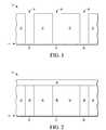
- FIG. 1Shown in FIG. 1 is a device structure 10 comprising a portion of a wafer having a substrate 12 and MEMS region 14 on a front side of the wafer.
- Substrate 12may be silicon having cavities 16 , 18 , and 20 in which each cavity 16 , 18 , and 20 has on opening on the backside of the wafer.
- MEMS region 14comprises a MEMS structure 22 , a MEMS structure 24 , and a MEMS structure 26 aligned to cavities 16 , 18 , and 20 , respectively.
- Cavities 16 , 18 , and 20may be about 200 to 1000 microns wide and about 700 microns deep.
- MEMS structuresextend about 30 microns past the edge of the cavity to which they are aligned. This extended region is primarily for support.
- the depthmay be established by the wafer thickness.
- a common thickness for 8 inch wafersis 725 microns which is a convenient dimension for the depth of cavities 16 , 18 , and 20 .
- Cavities 16 , 18 , and 20formed by an silicon etch that is selective to oxide. Oxide is used as an etch stop layer that is removed by an oxide etch after the silicon etch.
- MEMS structures 22 , 24 , and 26are for forming microphones so have diaphragms formed of silicon so the oxide etch is selective to silicon and will not harm the diaphragms and other structures of silicon that are part of MEMS structures 22 , 24 , and 26 . Sound will be received on the front side which is the side away from cavities 16 , 18 , and 20 .
- cavities 16 , 18 , and 20need to be covered to block sound from the backside of MEMS structures 22 , 24 , and 26 .
- the transfer from sound energy to electrical energy of a microphoneis performed by the MEMS structure having movement that is responsive to sound and causes a change in capacitance which can be detected electrically.
- the soundcomes from only one side of the diaphragm to establish a pressure differential which is the reason the cavities need to be covered to block the sound from arriving at the backside.
- FIG. 2Shown in FIG. 2 is device structure 10 after rolling a dielectric dry film 28 over the backside of the wafer to cover cavities 16 , 18 , and 20 .
- the dielectric dry filmmay come in rolls so can be conveniently rolled onto the backside of the wafer.
- An effective pressure for causing the dielectric dry film to adhere well to siliconis about 20 milliPascals to 60 milliPascals.
- Dielectric dry film 28may be about 100 microns thick. Although pliable for purposes of rolling, dry dielectric film spanning 200 to 1000 microns is sufficiently rigid for microphone purposes. With dielectric dry film 28 completely covering the openings of cavities 16 , 18 , and 20 an effective seal against sound is formed for blocking sound from MEMS structures 22 , 24 , and 26 .
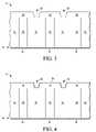
- FIG. 3Shown in FIG. 3 is device structure 10 after etching through dielectric dry film 28 in street regions 30 and 32 between cavities 16 , 18 , and 20 .
- the dry filmcan also be photosensitive and can be developed using conventional lithography and the developed portion can be easily removed in the manner of photoresist.
- the resultis that substrate 12 is exposed in street regions 30 and 32 .
- the width of exposure of substrate 12is about 100 microns. The width of exposure is preferably greater than the amount of loss along a street during a scribe operation.
- metal layer 34which may be aluminum, on dielectric dry film 28 and in street regions 30 and 32 . Because substrate 12 is exposed in street regions 30 and 32 , metal layer 34 is in contact with substrate 12 in street regions 30 and 32 .
- Metal layer 34may be deposited using conventional metal deposition techniques used in semiconductor manufacturing.
- FIG. 5Shown in FIG. 5 is a MEMS microphone 36 after a scribe operation along street regions 30 and 32 . This leaves MEMS structure 24 with cavity 18 . Also shown is that the scribe operation leaves a contact 38 between metal layer 34 and substrate 12 at street 30 . A similar contact remains between metal layer 34 and substrate 12 at street 32 .
- a microphone system 39comprising MEMS microphone 36 with solder balls 52 and 54 , a package substrate 40 , and an integrated circuit 42 with solder balls 56 , 58 , and 60 .
- Package substratehas contacts 44 , 46 , 48 , and 50 on its top surface.
- Solder ball 52is coupled to contact 44 .
- Solder ball 54is coupled to contact 46 .
- Solder ball 56is coupled to contact 46 .
- Solder ball 56is coupled to contact 48 .
- Solder ball 60is coupled to contact 50 .
- Integrated circuit 42functions to process capacitance change provided by MEMS microphone 36 in response to sound to electrical signals representative of the sound. Only two solder balls are shown attached to MEMS microphone 36 but others may be included. Sound is received between such solder balls.
- dielectric dry filmcompletely covers cavity 18 which is on the backside of MEMS structure 24 . Sound is received by MEMS microphone 36 along side MEMS microphone 36 and then between package substrate 40 and the front side of MEMS structure 24 . In the orientation shown, the front side of MEMS structure 24 and MEMS microphone 36 is the bottom of MEMS microphone 36 . This provides the benefit of the front side being protected physically because the front side is facing substrate 40 . The backside is covered so that a pressure differential can be established across the diaphragm.
- Metal layer 34can be made to contact substrate 12 and to provide an RF and EMI shield for MEMS structure 24 . Also, contact 38 , for example, between metal layer 34 and substrate 12 is made especially convenient by dielectric dry film being photosensitive so that substrate 12 can be exposed in street regions 30 and 32 very easily.
- a deviceincluding a substrate having a first side and a second side, the second side opposite the first side.
- the devicefurther includes a micro electro-mechanical systems (MEMS) structure formed on the first side of the substrate, and a cavity formed in the substrate directly opposite the MEMS structure, the cavity having an opening formed on the second side.
- the devicefurther includes a dielectric film attached to the second side of the substrate and completely covering the opening.
- the devicemay be further characterized by the MEMS structure including a diaphragm for a microphone.
- the devicemay be further characterized by the substrate including silicon.
- the devicemay be further characterized by the substrate being a semiconductor wafer.
- the devicemay be further characterized by the dielectric film including a photosensitive dielectric film.
- the devicemay be further characterized by the photosensitive dielectric film including a scribe street formed therein.
- the devicemay further include a metal layer formed on the dielectric film.
- the devicemay be further characterized by the metal layer including aluminum.
- a methodincluding providing a substrate having a first side and a second side, the second side opposite the first side.
- the methodfurther includes forming a micro electro-mechanical system (MEMS) structure on the first side of the substrate.
- MEMSmicro electro-mechanical system
- the methodfurther includes forming a cavity in the substrate directly opposite the MEMS structure, the cavity having an opening on the second side.
- the methodfurther includes attaching a dielectric film to the substrate and completely covering the opening.
- the methodmay further comprise forming a scribe street in the dielectric film to expose a predetermined portion of the second side of the substrate; forming a metal layer over dielectric film and over the second side of the substrate in the scribe street; and forming a cut in the substrate in the scribe street.
- the methodmay further comprise forming a bond pad on the first side of the substrate.
- the methodmay be further characterized by forming a metal layer further comprising forming a metal layer in electrical contact with the substrate.
- the methodmay be further characterized by forming the MEMS structure further comprising forming a MEMS microphone diaphragm.
- the methodmay be further characterized by forming the MEMS structure in a polysilicon layer on the first side of the substrate.
- the methodmay be further characterized by attaching the dielectric film to the substrate further comprising attaching a photosensitive dielectric film having an adhesive on one side.
- the methodmay further comprise photo exposing the photosensitive dielectric film to a radiation to remove the dielectric film from over a predetermined scribe street of the substrate.
- Described also is a methodincluding providing a substrate having a first side and a second side, the second side opposite the first side.
- the methodfurther includes forming a micro electro-mechanical system (MEMS) microphone diaphragm on the first side of the substrate.
- the methodfurther includes forming a cavity in the substrate directly opposite the MEMS microphone diaphragm, the cavity having an opening on the second side.
- the methodfurther includes attaching a photosensitive dielectric film to the substrate, the photosensitive dielectric film completely covering the opening.
- the methodfurther includes exposing a predetermined portion of the photosensitive dielectric film to a radiation to remove a first portion of the photosensitive dielectric film from over the substrate in the predetermined portion and to leave a second portion of the photosensitive dielectric film over the opening.
- the methodfurther includes forming a metal layer over the second portion of photosensitive dielectric film and contacting the substrate at the predetermined portion.
- the methodmay be further characterized by providing the substrate further comprising providing a silicon wafer.
- the methodmay further include forming a bond pad on the first side of the substrate.
- the methodmay be further characterized by forming the MEMS microphone diaphragm further comprising forming the MEMS microphone diaphragm in a polysilicon layer on the first side of the substrate.
- the substratewas described as being silicon but other materials may be effective.
- the MEMS systemwas shown as being formed of two devices, but it may be beneficial for the MEMS structure and the circuitry to be formed on the same substrate. Accordingly, the specification and figures are to be regarded in an illustrative rather than a restrictive sense, and all such modifications are intended to be included within the scope of the present invention. Any benefits, advantages, or solutions to problems that are described herein with regard to specific embodiments are not intended to be construed as a critical, required, or essential feature or element of any or all the claims.
- Coupledis not intended to be limited to a direct coupling or a mechanical coupling.
Landscapes
- Physics & Mathematics (AREA)
- Engineering & Computer Science (AREA)
- Acoustics & Sound (AREA)
- Signal Processing (AREA)
- Electrostatic, Electromagnetic, Magneto- Strictive, And Variable-Resistance Transducers (AREA)
- Micromachines (AREA)
Abstract
Description
Claims (11)
Priority Applications (1)
| Application Number | Priority Date | Filing Date | Title |
|---|---|---|---|
| US12/432,377US8158492B2 (en) | 2009-04-29 | 2009-04-29 | MEMS microphone with cavity and method therefor |
Applications Claiming Priority (1)
| Application Number | Priority Date | Filing Date | Title |
|---|---|---|---|
| US12/432,377US8158492B2 (en) | 2009-04-29 | 2009-04-29 | MEMS microphone with cavity and method therefor |
Publications (2)
| Publication Number | Publication Date |
|---|---|
| US20100276767A1 US20100276767A1 (en) | 2010-11-04 |
| US8158492B2true US8158492B2 (en) | 2012-04-17 |
Family
ID=43029757
Family Applications (1)
| Application Number | Title | Priority Date | Filing Date |
|---|---|---|---|
| US12/432,377Expired - Fee RelatedUS8158492B2 (en) | 2009-04-29 | 2009-04-29 | MEMS microphone with cavity and method therefor |
Country Status (1)
| Country | Link |
|---|---|
| US (1) | US8158492B2 (en) |
Cited By (3)
| Publication number | Priority date | Publication date | Assignee | Title |
|---|---|---|---|---|
| US9181086B1 (en) | 2012-10-01 | 2015-11-10 | The Research Foundation For The State University Of New York | Hinged MEMS diaphragm and method of manufacture therof |
| US9266717B2 (en) | 2013-03-15 | 2016-02-23 | Versana Micro Inc | Monolithically integrated multi-sensor device on a semiconductor substrate and method therefor |
| US12091313B2 (en) | 2019-08-26 | 2024-09-17 | The Research Foundation For The State University Of New York | Electrodynamically levitated actuator |
Families Citing this family (1)
| Publication number | Priority date | Publication date | Assignee | Title |
|---|---|---|---|---|
| US8948420B2 (en) | 2011-08-02 | 2015-02-03 | Robert Bosch Gmbh | MEMS microphone |
Citations (18)
| Publication number | Priority date | Publication date | Assignee | Title |
|---|---|---|---|---|
| US4555630A (en) | 1983-02-28 | 1985-11-26 | Tamarack Scientific Co., Inc. | Automatic system for exposing and handling double-sided printed circuit boards |
| US6521513B1 (en)* | 2000-07-05 | 2003-02-18 | Eastman Kodak Company | Silicon wafer configuration and method for forming same |
| US6522762B1 (en) | 1999-09-07 | 2003-02-18 | Microtronic A/S | Silicon-based sensor system |
| US6675472B1 (en) | 1999-04-29 | 2004-01-13 | Unicap Electronics Industrial Corporation | Process and structure for manufacturing plastic chip carrier |
| US20040016995A1 (en) | 2002-07-25 | 2004-01-29 | Kuo Shun Meen | MEMS control chip integration |
| US20040091125A1 (en) | 2001-06-15 | 2004-05-13 | Textron Systems Corporation | Systems and methods for sensing an acoustic signal using microelectromechanical systems technology |
| US6781231B2 (en) | 2002-09-10 | 2004-08-24 | Knowles Electronics Llc | Microelectromechanical system package with environmental and interference shield |
| US6788795B2 (en) | 2000-12-22 | 2004-09-07 | Brüel & Kjaer Sound & Vibration Measurement A/S | Micromachined capacitive component with high stability |
| US20070009111A1 (en) | 2005-07-06 | 2007-01-11 | Sonion A/S | Microphone assembly with P-type preamplifier input stage |
| US7166910B2 (en) | 2000-11-28 | 2007-01-23 | Knowles Electronics Llc | Miniature silicon condenser microphone |
| US20070041597A1 (en) | 2005-08-20 | 2007-02-22 | Song Chung-Dam | Silicon based condenser microphone and packaging method for the same |
| US7202552B2 (en) | 2005-07-15 | 2007-04-10 | Silicon Matrix Pte. Ltd. | MEMS package using flexible substrates, and method thereof |
| US20070165888A1 (en)* | 2005-04-25 | 2007-07-19 | Analog Devices, Inc. | Support Apparatus for Microphone Diaphragm |
| US20080075309A1 (en)* | 2006-09-08 | 2008-03-27 | Industrial Technology Research Institute | Structure and manufacturing method of inversed microphone chip component |
| US7381589B2 (en) | 2000-11-28 | 2008-06-03 | Knowles Electronics, Llc | Silicon condenser microphone and manufacturing method |
| US20080175417A1 (en) | 2005-05-16 | 2008-07-24 | Sensfab Pte Ltd. | Silicon Microphone |
| US20080185699A1 (en)* | 2007-02-06 | 2008-08-07 | Advanced Semiconductor Engineering Inc. | Microelectromechanical system package and the method for manufacturing the same |
| US20090169035A1 (en)* | 2006-03-30 | 2009-07-02 | Pulse Mems Aps | Single Die MEMS Acoustic Transducer and Manufacturing Method |
- 2009
- 2009-04-29USUS12/432,377patent/US8158492B2/ennot_activeExpired - Fee Related
Patent Citations (20)
| Publication number | Priority date | Publication date | Assignee | Title |
|---|---|---|---|---|
| US4555630A (en) | 1983-02-28 | 1985-11-26 | Tamarack Scientific Co., Inc. | Automatic system for exposing and handling double-sided printed circuit boards |
| US6675472B1 (en) | 1999-04-29 | 2004-01-13 | Unicap Electronics Industrial Corporation | Process and structure for manufacturing plastic chip carrier |
| US6522762B1 (en) | 1999-09-07 | 2003-02-18 | Microtronic A/S | Silicon-based sensor system |
| US20030128854A1 (en) | 1999-09-07 | 2003-07-10 | Matthias Mullenborn | Surface mountable transducer system |
| US6521513B1 (en)* | 2000-07-05 | 2003-02-18 | Eastman Kodak Company | Silicon wafer configuration and method for forming same |
| US7166910B2 (en) | 2000-11-28 | 2007-01-23 | Knowles Electronics Llc | Miniature silicon condenser microphone |
| US7381589B2 (en) | 2000-11-28 | 2008-06-03 | Knowles Electronics, Llc | Silicon condenser microphone and manufacturing method |
| US7242089B2 (en) | 2000-11-28 | 2007-07-10 | Knowles Electronics, Llc | Miniature silicon condenser microphone |
| US6788795B2 (en) | 2000-12-22 | 2004-09-07 | Brüel & Kjaer Sound & Vibration Measurement A/S | Micromachined capacitive component with high stability |
| US20040091125A1 (en) | 2001-06-15 | 2004-05-13 | Textron Systems Corporation | Systems and methods for sensing an acoustic signal using microelectromechanical systems technology |
| US20040016995A1 (en) | 2002-07-25 | 2004-01-29 | Kuo Shun Meen | MEMS control chip integration |
| US6781231B2 (en) | 2002-09-10 | 2004-08-24 | Knowles Electronics Llc | Microelectromechanical system package with environmental and interference shield |
| US20070165888A1 (en)* | 2005-04-25 | 2007-07-19 | Analog Devices, Inc. | Support Apparatus for Microphone Diaphragm |
| US20080175417A1 (en) | 2005-05-16 | 2008-07-24 | Sensfab Pte Ltd. | Silicon Microphone |
| US20070009111A1 (en) | 2005-07-06 | 2007-01-11 | Sonion A/S | Microphone assembly with P-type preamplifier input stage |
| US7202552B2 (en) | 2005-07-15 | 2007-04-10 | Silicon Matrix Pte. Ltd. | MEMS package using flexible substrates, and method thereof |
| US20070041597A1 (en) | 2005-08-20 | 2007-02-22 | Song Chung-Dam | Silicon based condenser microphone and packaging method for the same |
| US20090169035A1 (en)* | 2006-03-30 | 2009-07-02 | Pulse Mems Aps | Single Die MEMS Acoustic Transducer and Manufacturing Method |
| US20080075309A1 (en)* | 2006-09-08 | 2008-03-27 | Industrial Technology Research Institute | Structure and manufacturing method of inversed microphone chip component |
| US20080185699A1 (en)* | 2007-02-06 | 2008-08-07 | Advanced Semiconductor Engineering Inc. | Microelectromechanical system package and the method for manufacturing the same |
Non-Patent Citations (2)
| Title |
|---|
| Non-final Office Action dated Jan. 21, 2011 in U.S. Appl. No. 12/432,289. |
| U.S. Appl. No. 12/432,289, filed Apr. 29, 2009, Office Action-Rejection, mailed Sep. 1, 2011. |
Cited By (13)
| Publication number | Priority date | Publication date | Assignee | Title |
|---|---|---|---|---|
| US9554213B2 (en) | 2012-10-01 | 2017-01-24 | The Research Foundation For The State University Of New York | Hinged MEMS diaphragm |
| US9906869B2 (en) | 2012-10-01 | 2018-02-27 | The Research Foundation For The State University Of New York | Hinged MEMS diaphragm, and method of manufacture thereof |
| US9181086B1 (en) | 2012-10-01 | 2015-11-10 | The Research Foundation For The State University Of New York | Hinged MEMS diaphragm and method of manufacture therof |
| US9862594B2 (en) | 2013-03-15 | 2018-01-09 | Versana Micro Inc. | Wearable device having a monolithically integrated multi-sensor device on a semiconductor substrate and method therefor |
| US9580302B2 (en) | 2013-03-15 | 2017-02-28 | Versana Micro Inc. | Cell phone having a monolithically integrated multi-sensor device on a semiconductor substrate and method therefor |
| US9758368B2 (en) | 2013-03-15 | 2017-09-12 | Versana Micro Inc | Monolithically integrated multi-sensor device on a semiconductor substrate and method therefor |
| US9327965B2 (en) | 2013-03-15 | 2016-05-03 | Versana Micro Inc | Transportation device having a monolithically integrated multi-sensor device on a semiconductor substrate and method therefor |
| US9890038B2 (en) | 2013-03-15 | 2018-02-13 | Versana Micro Inc. | Monolithically integrated multi-sensor device on a semiconductor substrate and method therefor |
| US9266717B2 (en) | 2013-03-15 | 2016-02-23 | Versana Micro Inc | Monolithically integrated multi-sensor device on a semiconductor substrate and method therefor |
| US10280074B2 (en) | 2013-03-15 | 2019-05-07 | Versana Micro Inc | Monolithically integrated multi-sensor device on a semiconductor substrate and method therefor |
| US10508026B2 (en) | 2013-03-15 | 2019-12-17 | Versana Micro Inc. | Monolithically integrated multi-sensor device on a semiconductor substrate and method therefor |
| US11174154B2 (en) | 2013-03-15 | 2021-11-16 | Versana Micro Inc. | Monolithically integrated multi-sensor device on a semiconductor substrate and method therefor |
| US12091313B2 (en) | 2019-08-26 | 2024-09-17 | The Research Foundation For The State University Of New York | Electrodynamically levitated actuator |
Also Published As
| Publication number | Publication date |
|---|---|
| US20100276767A1 (en) | 2010-11-04 |
Similar Documents
| Publication | Publication Date | Title |
|---|---|---|
| TWI404671B (en) | Mems device | |
| US8098870B2 (en) | Silicon microphone | |
| US8497149B2 (en) | MEMS device | |
| US9783408B2 (en) | Structure of MEMS electroacoustic transducer | |
| EP3468226B1 (en) | Mems microphone and preparation method thereof | |
| US20230234837A1 (en) | Mems microphone with an anchor | |
| US8330239B2 (en) | Shielding for a micro electro-mechanical device and method therefor | |
| US20110073967A1 (en) | Apparatus and method of forming a mems acoustic transducer with layer transfer processes | |
| US8755541B2 (en) | Microphone with parasitic capacitance cancelation | |
| US20230239641A1 (en) | Method of making mems microphone with an anchor | |
| EP1632105B1 (en) | Fabrication of silicon microphones | |
| US8158492B2 (en) | MEMS microphone with cavity and method therefor | |
| US8569850B2 (en) | Ultra low pressure sensor | |
| CN111277937A (en) | MEMS microphone and manufacturing method thereof | |
| US20150060954A1 (en) | CMOS-MEMS Integrated Flow for Making a Pressure Sensitive Transducer | |
| US20080185669A1 (en) | Silicon Microphone | |
| CN211980613U (en) | MEMS 5G communication radio frequency antenna | |
| US7343661B2 (en) | Method for making condenser microphones | |
| KR100327326B1 (en) | Manufacturing method of S.O.wafer | |
| GB2455214A (en) | MEMS microphone array |
Legal Events
| Date | Code | Title | Description |
|---|---|---|---|
| AS | Assignment | Owner name:FREESCALE SEMICONDUCTOR, INC., TEXAS Free format text:ASSIGNMENT OF ASSIGNORS INTEREST;ASSIGNORS:LIU, LIANJUN;MITCHELL, DOUGLAS G.;REEL/FRAME:023068/0022 Effective date:20090416 | |
| AS | Assignment | Owner name:CITIBANK, N.A., NEW YORK Free format text:SECURITY AGREEMENT;ASSIGNOR:FREESCALE SEMICONDUCTOR, INC.;REEL/FRAME:023273/0099 Effective date:20090804 | |
| STCF | Information on status: patent grant | Free format text:PATENTED CASE | |
| AS | Assignment | Owner name:CITIBANK, N.A., AS NOTES COLLATERAL AGENT, NEW YORK Free format text:SECURITY AGREEMENT;ASSIGNOR:FREESCALE SEMICONDUCTOR, INC.;REEL/FRAME:030633/0424 Effective date:20130521 Owner name:CITIBANK, N.A., AS NOTES COLLATERAL AGENT, NEW YOR Free format text:SECURITY AGREEMENT;ASSIGNOR:FREESCALE SEMICONDUCTOR, INC.;REEL/FRAME:030633/0424 Effective date:20130521 | |
| AS | Assignment | Owner name:CITIBANK, N.A., AS NOTES COLLATERAL AGENT, NEW YORK Free format text:SECURITY AGREEMENT;ASSIGNOR:FREESCALE SEMICONDUCTOR, INC.;REEL/FRAME:031591/0266 Effective date:20131101 Owner name:CITIBANK, N.A., AS NOTES COLLATERAL AGENT, NEW YOR Free format text:SECURITY AGREEMENT;ASSIGNOR:FREESCALE SEMICONDUCTOR, INC.;REEL/FRAME:031591/0266 Effective date:20131101 | |
| FPAY | Fee payment | Year of fee payment:4 | |
| AS | Assignment | Owner name:FREESCALE SEMICONDUCTOR, INC., TEXAS Free format text:PATENT RELEASE;ASSIGNOR:CITIBANK, N.A., AS COLLATERAL AGENT;REEL/FRAME:037354/0823 Effective date:20151207 | |
| AS | Assignment | Owner name:MORGAN STANLEY SENIOR FUNDING, INC., MARYLAND Free format text:ASSIGNMENT AND ASSUMPTION OF SECURITY INTEREST IN PATENTS;ASSIGNOR:CITIBANK, N.A.;REEL/FRAME:037486/0517 Effective date:20151207 | |
| AS | Assignment | Owner name:MORGAN STANLEY SENIOR FUNDING, INC., MARYLAND Free format text:ASSIGNMENT AND ASSUMPTION OF SECURITY INTEREST IN PATENTS;ASSIGNOR:CITIBANK, N.A.;REEL/FRAME:037518/0292 Effective date:20151207 | |
| AS | Assignment | Owner name:NORTH STAR INNOVATIONS INC., CALIFORNIA Free format text:ASSIGNMENT OF ASSIGNORS INTEREST;ASSIGNOR:FREESCALE SEMICONDUCTOR, INC.;REEL/FRAME:037694/0264 Effective date:20151002 | |
| AS | Assignment | Owner name:NXP, B.V., F/K/A FREESCALE SEMICONDUCTOR, INC., NETHERLANDS Free format text:RELEASE BY SECURED PARTY;ASSIGNOR:MORGAN STANLEY SENIOR FUNDING, INC.;REEL/FRAME:040925/0001 Effective date:20160912 Owner name:NXP, B.V., F/K/A FREESCALE SEMICONDUCTOR, INC., NE Free format text:RELEASE BY SECURED PARTY;ASSIGNOR:MORGAN STANLEY SENIOR FUNDING, INC.;REEL/FRAME:040925/0001 Effective date:20160912 | |
| AS | Assignment | Owner name:NXP B.V., NETHERLANDS Free format text:RELEASE BY SECURED PARTY;ASSIGNOR:MORGAN STANLEY SENIOR FUNDING, INC.;REEL/FRAME:040928/0001 Effective date:20160622 | |
| AS | Assignment | Owner name:MORGAN STANLEY SENIOR FUNDING, INC., MARYLAND Free format text:CORRECTIVE ASSIGNMENT TO CORRECT THE REMOVE PATENTS 8108266 AND 8062324 AND REPLACE THEM WITH 6108266 AND 8060324 PREVIOUSLY RECORDED ON REEL 037518 FRAME 0292. ASSIGNOR(S) HEREBY CONFIRMS THE ASSIGNMENT AND ASSUMPTION OF SECURITY INTEREST IN PATENTS;ASSIGNOR:CITIBANK, N.A.;REEL/FRAME:041703/0536 Effective date:20151207 | |
| AS | Assignment | Owner name:SHENZHEN XINGUODU TECHNOLOGY CO., LTD., CHINA Free format text:CORRECTIVE ASSIGNMENT TO CORRECT THE TO CORRECT THE APPLICATION NO. FROM 13,883,290 TO 13,833,290 PREVIOUSLY RECORDED ON REEL 041703 FRAME 0536. ASSIGNOR(S) HEREBY CONFIRMS THE THE ASSIGNMENT AND ASSUMPTION OF SECURITYINTEREST IN PATENTS.;ASSIGNOR:MORGAN STANLEY SENIOR FUNDING, INC.;REEL/FRAME:048734/0001 Effective date:20190217 | |
| FEPP | Fee payment procedure | Free format text:MAINTENANCE FEE REMINDER MAILED (ORIGINAL EVENT CODE: REM.); ENTITY STATUS OF PATENT OWNER: LARGE ENTITY | |
| AS | Assignment | Owner name:MORGAN STANLEY SENIOR FUNDING, INC., MARYLAND Free format text:CORRECTIVE ASSIGNMENT TO CORRECT THE REMOVE APPLICATION11759915 AND REPLACE IT WITH APPLICATION 11759935 PREVIOUSLY RECORDED ON REEL 037486 FRAME 0517. ASSIGNOR(S) HEREBY CONFIRMS THE ASSIGNMENT AND ASSUMPTION OF SECURITYINTEREST IN PATENTS;ASSIGNOR:CITIBANK, N.A.;REEL/FRAME:053547/0421 Effective date:20151207 | |
| AS | Assignment | Owner name:NXP B.V., NETHERLANDS Free format text:CORRECTIVE ASSIGNMENT TO CORRECT THE REMOVEAPPLICATION 11759915 AND REPLACE IT WITH APPLICATION11759935 PREVIOUSLY RECORDED ON REEL 040928 FRAME 0001. ASSIGNOR(S) HEREBY CONFIRMS THE RELEASE OF SECURITYINTEREST;ASSIGNOR:MORGAN STANLEY SENIOR FUNDING, INC.;REEL/FRAME:052915/0001 Effective date:20160622 | |
| AS | Assignment | Owner name:NXP, B.V. F/K/A FREESCALE SEMICONDUCTOR, INC., NETHERLANDS Free format text:CORRECTIVE ASSIGNMENT TO CORRECT THE REMOVEAPPLICATION 11759915 AND REPLACE IT WITH APPLICATION11759935 PREVIOUSLY RECORDED ON REEL 040925 FRAME 0001. ASSIGNOR(S) HEREBY CONFIRMS THE RELEASE OF SECURITYINTEREST;ASSIGNOR:MORGAN STANLEY SENIOR FUNDING, INC.;REEL/FRAME:052917/0001 Effective date:20160912 | |
| LAPS | Lapse for failure to pay maintenance fees | Free format text:PATENT EXPIRED FOR FAILURE TO PAY MAINTENANCE FEES (ORIGINAL EVENT CODE: EXP.); ENTITY STATUS OF PATENT OWNER: LARGE ENTITY | |
| STCH | Information on status: patent discontinuation | Free format text:PATENT EXPIRED DUE TO NONPAYMENT OF MAINTENANCE FEES UNDER 37 CFR 1.362 | |
| FP | Lapsed due to failure to pay maintenance fee | Effective date:20200417 |