US8154317B2 - Integrated circuit device to support inductive sensing - Google Patents
Integrated circuit device to support inductive sensingDownload PDFInfo
- Publication number
- US8154317B2 US8154317B2US12/560,855US56085509AUS8154317B2US 8154317 B2US8154317 B2US 8154317B2US 56085509 AUS56085509 AUS 56085509AUS 8154317 B2US8154317 B2US 8154317B2
- Authority
- US
- United States
- Prior art keywords
- inductive
- external connection
- coil
- clock
- inductive touch
- Prior art date
- Legal status (The legal status is an assumption and is not a legal conclusion. Google has not performed a legal analysis and makes no representation as to the accuracy of the status listed.)
- Expired - Fee Related, expires
Links
- 230000001939inductive effectEffects0.000titleclaimsabstractdescription130
- 230000001360synchronised effectEffects0.000claimsdescription44
- 230000008878couplingEffects0.000claimsdescription11
- 238000010168coupling processMethods0.000claimsdescription11
- 238000005859coupling reactionMethods0.000claimsdescription11
- 238000005259measurementMethods0.000claimsdescription4
- 230000008859changeEffects0.000abstractdescription4
- 230000009471actionEffects0.000abstractdescription2
- 238000006073displacement reactionMethods0.000abstract1
- 238000010586diagramMethods0.000description12
- 239000011159matrix materialSubstances0.000description5
- 239000003990capacitorSubstances0.000description4
- 230000008901benefitEffects0.000description3
- 230000004048modificationEffects0.000description3
- 238000012986modificationMethods0.000description3
- 241001644893Entandrophragma utileSpecies0.000description2
- 238000013461designMethods0.000description2
- 238000001514detection methodMethods0.000description2
- 238000012545processingMethods0.000description2
- 230000004075alterationEffects0.000description1
- 230000000903blocking effectEffects0.000description1
- 238000005516engineering processMethods0.000description1
- 230000005284excitationEffects0.000description1
- 239000011888foilSubstances0.000description1
- 239000007788liquidSubstances0.000description1
- 238000004519manufacturing processMethods0.000description1
- 230000007246mechanismEffects0.000description1
- 238000000034methodMethods0.000description1
- 238000003825pressingMethods0.000description1
- 230000008569processEffects0.000description1
- 230000035945sensitivityEffects0.000description1
Images


Classifications
- H—ELECTRICITY
- H03—ELECTRONIC CIRCUITRY
- H03K—PULSE TECHNIQUE
- H03K17/00—Electronic switching or gating, i.e. not by contact-making and –breaking
- H03K17/94—Electronic switching or gating, i.e. not by contact-making and –breaking characterised by the way in which the control signals are generated
- H03K17/96—Touch switches
- H—ELECTRICITY
- H03—ELECTRONIC CIRCUITRY
- H03K—PULSE TECHNIQUE
- H03K2217/00—Indexing scheme related to electronic switching or gating, i.e. not by contact-making or -breaking covered by H03K17/00
- H03K2217/94—Indexing scheme related to electronic switching or gating, i.e. not by contact-making or -breaking covered by H03K17/00 characterised by the way in which the control signal is generated
- H03K2217/96—Touch switches
- H03K2217/96038—Inductive touch switches
Definitions
- the present disclosurerelates to integrated circuits, and more particularly to, an integrated circuit device that supports inductive sensing.
- Capacitive sensorse.g., touch sensors
- capacitive touch sensorssuffer from several shortcomings such as sensitivity to spilled liquids and unreliable operation when a user is wearing heavy gloves.
- Inductive touch sensorssolve the shortcomings of capacitive touch sensors and have started to replace them in certain specialized applications not completely suited for the capacitive touch sensors.
- Inductive touch sensorsrequire appropriate specialized interface circuits when used in an electronic system.
- Present technology inductive sensor interface circuitsrequire a significant number of external discrete components to operate. These external discrete components are expensive and require a large amount of circuit board area for use in a system application.
- the inductive sensormay be used to sense a touch causing an inductive change in the sensor.
- the integrated circuit interface that supports the operation of the inductive sensorwill have control mechanisms that substantially eliminate the need for external components, thus reducing physical size and costs of manufacture for systems using inductive sensors.
- an electronic system having an inductive touch interfacecomprises: an inductive touch interface comprising a plurality of inductive touch sensor coils and an inductive reference coil; a first integrated circuit digital processor; a second integrated circuit inductive touch analog front end comprising: a voltage reference; a synchronous detector having a first input coupled to the inductive reference coil; a second input coupled to the plurality of inductive touch sensor coils; a third input coupled to a reference select signal from the digital processor; a fourth input coupled to a clock signal from the digital processor, and a fifth input coupled to the voltage reference; a coil driver having an output coupled in series with the inductive reference coil and selected ones of the plurality of inductive touch sensor coils, an input coupled through an external low-pass filter to a clock output from the digital processor; and an amplifier configured with a low-pass filter and having inputs coupled to the synchronous detector and an output having voltage values representative of inductance values of the plurality of inductive touch sensor coils and the inductive reference coil, the output of
- the synchronous detectormay comprise: a decoder having a first input coupled to the clock external connection and a second input coupled to the reference select external connection; and six analog pass-gates controlled by the decoder, wherein inputs of first and fourth analog pass-gates are coupled to the voltage reference, inputs of second and fifth analog pass-gates are coupled to the plurality of inductive touch sensor coils, inputs of third and sixth analog pass-gates are coupled to the inductive reference coil; whereby the third and fourth analog pass-gates are closed when the reference select and clock signals are at first logic levels, the first and sixth analog pass-gates are closed when the reference select signal is at the first logic level and the clock signal is at a second logic level, the second and fourth analog pass-gates are closed when the reference select signal is at the second logic level and the clock signal is at the first logic level, and the first and fifth analog pass-gates are closed when the reference select and clock signals are at the second logic level.
- the synchronous detectormay also comprise: a frequency mixer; a decoder having a first input coupled to the clock and a second input coupled to the reference; and a plurality of multiplexers for selectively coupling the voltage reference, the inductive touch sensor, and the inductive reference coil external connection to the frequency mixer.
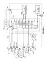
- FIG. 1is a schematic block diagram of an electronic system having an inductive touch keypad, an inductive touch analog front end and a digital processor, according to a specific example embodiment of this disclosure
- FIG. 2is a more detailed schematic block diagram of the inductive touch analog front end shown in FIG. 1 ;
- FIG. 3is a more detailed schematic block diagram of a synchronous detector and the circuit functions shown in FIG. 2 , according to a specific example embodiment of this disclosure;
- FIG. 4is a more detailed schematic block diagram of a synchronous detector and the circuit functions shown in FIG. 2 , according to another specific example embodiment of this disclosure;
- FIG. 5is a more detailed schematic block diagram of the amplifier and low-pass filter shown in FIG. 3 , according to a specific example embodiment of this disclosure.
- FIG. 6is a more detailed schematic block diagram of the amplifier and low-pass filter shown in FIG. 4 , according to another specific example embodiment of this disclosure.
- FIG. 1depicted is a schematic block diagram of an electronic system having an inductive touch keypad, an inductive touch analog front end and a digital processor, according to a specific example embodiment of this disclosure.
- a digital processor 106e.g., a microprocessor, microcomputer, digital signal processor (DSP), application specific integrated circuit (ASIC), programmable logic array (PLA), etC., is coupled to an inductive touch analog front end (AFE) 104 and a matrix of inductive touch sensors 102 .
- AFEinductive touch analog front end
- Preferred inductive touch sensors 102are Microchip inductive mTouchTM sensors more fully described at www.microchip.com.
- the inductive touch AFE 104facilitates, with a single low-cost integrated circuit device, all active functions used in determining when there is actuation of inductive sensors, e.g., by pressing and deflecting a target key that changes the inductance value of an associated inductive sensor.
- the inductive touch AFE 104measures the inductance value of each key of the matrix of inductive touch sensors 102 and converts the inductance values into respective analog direct current (dc) voltages that are read and converted into digital values by the digital processor 106 .
- a reference inductore.g., coil
- FIGS. 2 and 3may also be included in the matrix of inductive touch sensors 102 for use as a comparison reference between an un-activated inductive sensor (coil) and an activated inductive sensor (coil), as more fully described hereinafter.
- the digital processor 106supplies clock and control functions to the inductive touch AFE 104 , reads the analog voltage detector output of the inductive touch AFE 104 , and selects each key of the matrix of inductive touch sensors 102 and the reference inductive sensor for processing by the inductive touch AFE 104 , as more fully described hereinafter. When actuation of a key of the matrix of inductive touch sensors 102 is determined, the digital processor 106 will take an appropriate action.
- the inductive touch AFE 104comprises a synchronous detector 212 , a control module 214 , a coil driver 210 , a voltage reference 220 , and an amplifier/low-pass filter 216 .
- the synchronous detector 212is used to extract signals from excitation of each touch sensor coil.
- Use of a synchronous detectore.g., mixer
- the alternating current (AC) voltage amplitude from each touch sensor coilis mixed with a clock signal to produce sum and difference frequencies of the two AC signals. Since the AC voltage amplitude from each inductive touch sensor coil is at the same frequency as the clock signal, there will be a direct current (DC) voltage component (difference frequency) and twice the clock signal frequency (sum frequency) signals as mixing products from the synchronous detector 212 .
- DCdirect current
- the amplifier/low-pass filter 216is used as a buffer-amplifier/low pass filter between the synchronous detector 212 and the V DETOUT node 236 .
- the amplifier/low-pass filter 216functions as an integrator and passes the DC voltage (difference frequency mixing result) while effectively suppressing the twice clock frequency (sum frequency mixing result).
- a DC voltageis available to the digital processor 106 that is proportional to the inductance value of a selected one of the plurality of inductive sensors 242 or the reference inductor 240 , as more fully described hereinafter.
- the digital processor 106converts the analog DC voltage from the inductive touch AFE 104 to a digital voltage representation thereof and associates that digital voltage representation with the selected inductive sensor 242 or reference inductor 240 . Since the digital processor 106 selects the inductive sensor 242 or the reference inductor 240 , matching of the DC voltage values to associated ones of the plurality of inductive sensors 242 and reference inductor 240 are easily made.
- the voltage reference 220may be set to have a voltage output of approximately one-half the supply voltage, and may be an operational amplifier configured with unity gain and a non-inverting input to a resister ladder voltage divider. Other types of voltage references may be used effectively so long as there is adequate voltage stability and sufficient low impedance drive capability.
- the coil driver 210receives a signal derived from the clock supplied by the digital processor 106 or from any other clock source available.
- a low-pass filtercomprising capacitor 252 and resistor 250 attenuate the higher frequency components of the clock square wave signal so as to produce approximately a sinusoidal waveform that is input to the coil driver 210 , amplified, and then made available to the plurality of inductive sensors 242 and the reference inductor 240 through a series connected resistor 244 .
- Each of the plurality of inductive sensors 242is selected by the digital processor 106 by connecting one end of the selected one of the plurality of inductive sensors 242 to a supply common, thereby completing the circuit from the coil driver 210 and producing a voltage across the selected one of the plurality of inductive sensors 242 from the AC current supplied by the coil driver 210 .
- the synchronous detector 212detects the voltage from each one of the plurality of inductive sensors 242 and the reference inductor 240 for subsequent processing by the digital processor 106 .
- the coil driver 210supplies current at the clock frequency to the reference coil 240 and the selected one of the plurality of inductive sensors 242 connected in series. When the approximately sinusoidal current is flowing through the reference coil 240 and the selected one of the plurality of inductive sensors 242 , voltages proportional to the inductances are thereby generated.
- the synchronous detector 212 acomprises a decoder 360 and a plurality of analog pass-gates 362 .
- the decoder 360receives a clock (C LK ) signal at external connection 230 and an input selection (R EFSEL ) at external connection 228 , both from the digital processor 106 .
- the decoder 360controls the on and off states of the plurality of analog pass-gates 362 , as more fully described hereinafter.
- the coil driver 210generates AC voltages across the reference inductor 240 and the selected one of the plurality of inductive sensors 242 proportional to the inductances thereof.
- the selected one of the plurality of inductive sensor voltages (L BTN ) and the reference inductor voltage (L REF )are coupled through DC blocking capacitors 246 and 248 to inputs of the synchronous detector 212 a through external connections 224 and 226 , respectively.
- the plurality of analog pass-gates 362may operate according to the following table:
- the synchronous detector 212 ahas three signal inputs used for measurement of the inductance of the inductive touch sensors, the reference inductor voltage (L REF ), the selected one of the plurality of inductive sensor voltage (L BTN ) and the reference voltage (V REF ) from the voltage reference 220 .
- the synchronous detector 212 a(mixer) can mix between two of the these three inputs at any given time at the frequency provided at the clock connection 230 (C LK ). For example, if R EFSEL is at a logic zero, then the synchronous detector 212 a mixes the reference inductor voltage and reference voltage signals.
- the differential amplifier/low-pass filter 216 ais used as a buffer-amplifier/low pass filter between the synchronous detector 212 a and the V DETOUT node 236 .
- the amplifier/low-pass filter 216 afunctions as an integrator and passes the DC voltage (difference frequency mixing result) while effectively suppressing the twice clock frequency (sum frequency mixing result).
- This DC voltagerepresents the inductance of the measured reference or selected touch sensor inductor, as discussed more fully above.
- the DC voltagemay be fed to an analog-to-digital converter (ADC) (not shown) that is part of the digital processor 106 , whereby the digital processor 106 samples and performs inductive touch calculations in determining when a touch sensor is actuated.
- ADCanalog-to-digital converter
- frequency mixingoccurs that produces the sum and the difference frequencies between the clock input frequency and the frequency of the coil voltage. Since both frequencies are the same (the output of the coil driver 210 is derived from the clock signal input) the mixing product sum of the frequencies will be twice the clock frequency and the difference of the frequencies will be at zero frequency, a DC voltage that is proportional to the inductance value of the measured coil.
- the differential outputs from the closed ones of the plurality of analog pass-gates 362are applied to the differential inputs of the amplifier/low-pass filter 216 a .
- the voltage reference 220DC biases the circuits of the synchronous detector 212 a at about one-half the operating voltage for optimal operation of the amplifier/low-pass filter 216 a .
- the amplifier/low-pass filter 216 aconverts the differential output from the synchronous detector 212 a to a single-ended voltage output, whereby DC utile (useful, desired) signals are made available to an analog input of the digital processor 106 .
- An isolate signalmay be applied at node 250 to turn off all of the plurality of analog pass-gates 362 so as to isolate the amplifier/low-pass filter 216 a from the plurality of inductive sensors 242 and the inductive sensor 240 during a Vref measurement at node 252 , otherwise during normal operation the synchronous detector 212 a functions as described hereinabove.
- the amplifier/low-pass filter 216 bmay comprise an amplifier 550 having differential inputs, e.g., differential input operational amplifier; feedback resistor 260 , and capacitor 264 arranged in a low-pass filter configuration. It is contemplated and within the scope of this disclosure that other amplifier and low pass filter configurations may be used for the amplifier/low-pass filter 216 b , as would be know to one of ordinary skill in analog circuit design and having the benefit of this disclosure.
Landscapes
- Electronic Switches (AREA)
- Amplifiers (AREA)
Abstract
Description
| REFSEL | CLK | Tx1 | Tx2 | Tx3 | Tx4 | Tx5 | Tx6 | Remarks |
| 0 | 0 | open | open | close | close | open | open | LREF |
| selected | ||||||||
| 0 | 1 | close | open | open | open | open | close | LREF |
| selected | ||||||||
| 1 | 0 | open | close | open | close | open | open | LBTN |
| selected | ||||||||
| 1 | 1 | close | open | open | open | close | open | LBTN |
| selected | ||||||||
Claims (21)
Priority Applications (6)
| Application Number | Priority Date | Filing Date | Title |
|---|---|---|---|
| US12/560,855US8154317B2 (en) | 2008-10-09 | 2009-09-16 | Integrated circuit device to support inductive sensing |
| KR1020107028978AKR101385650B1 (en) | 2008-10-09 | 2009-09-30 | Integrated circuit device supporting inductive sensing |
| CN200980129346.9ACN102106086B (en) | 2008-10-09 | 2009-09-30 | Integrated circuit device supporting inductive sensing |
| EP09793171AEP2332255B1 (en) | 2008-10-09 | 2009-09-30 | Integrated circuit device supporting inductive sensing |
| PCT/US2009/059000WO2010042363A1 (en) | 2008-10-09 | 2009-09-30 | Integrated circuit device supporting inductive sensing |
| TW098133999ATWI526911B (en) | 2008-10-09 | 2009-10-07 | Integrated circuit device to support inductive sensing |
Applications Claiming Priority (2)
| Application Number | Priority Date | Filing Date | Title |
|---|---|---|---|
| US10401208P | 2008-10-09 | 2008-10-09 | |
| US12/560,855US8154317B2 (en) | 2008-10-09 | 2009-09-16 | Integrated circuit device to support inductive sensing |
Publications (2)
| Publication Number | Publication Date |
|---|---|
| US20100090716A1 US20100090716A1 (en) | 2010-04-15 |
| US8154317B2true US8154317B2 (en) | 2012-04-10 |
Family
ID=42098295
Family Applications (2)
| Application Number | Title | Priority Date | Filing Date |
|---|---|---|---|
| US12/560,906Expired - Fee RelatedUS8378660B2 (en) | 2008-10-09 | 2009-09-16 | Programmable integrated circuit device to support inductive sensing |
| US12/560,855Expired - Fee RelatedUS8154317B2 (en) | 2008-10-09 | 2009-09-16 | Integrated circuit device to support inductive sensing |
Family Applications Before (1)
| Application Number | Title | Priority Date | Filing Date |
|---|---|---|---|
| US12/560,906Expired - Fee RelatedUS8378660B2 (en) | 2008-10-09 | 2009-09-16 | Programmable integrated circuit device to support inductive sensing |
Country Status (6)
| Country | Link |
|---|---|
| US (2) | US8378660B2 (en) |
| EP (2) | EP2332255B1 (en) |
| KR (2) | KR101718846B1 (en) |
| CN (2) | CN102119488B (en) |
| TW (2) | TW201030590A (en) |
| WO (2) | WO2010042361A2 (en) |
Cited By (4)
| Publication number | Priority date | Publication date | Assignee | Title |
|---|---|---|---|---|
| US20100090717A1 (en)* | 2008-10-09 | 2010-04-15 | Microchip Technology Incorporated | Programmable Integrated Circuit Device to Support Inductive Sensing |
| WO2013090338A1 (en) | 2011-12-14 | 2013-06-20 | Microchip Technology Incorporated | Capacitive/inductive proximity detection for wi-fi protection |
| US9709614B2 (en) | 2008-10-15 | 2017-07-18 | Azoteq (Pty) Ltd | Parasitic capacitance cancellation in capacitive measurement |
| US10527457B2 (en) | 2015-02-27 | 2020-01-07 | Azoteq (Pty) Ltd | Inductance sensing |
Families Citing this family (13)
| Publication number | Priority date | Publication date | Assignee | Title |
|---|---|---|---|---|
| KR101091005B1 (en) | 2009-11-06 | 2011-12-08 | 위니아만도 주식회사 | Input device using inductive sensor |
| TWI410640B (en)* | 2010-11-01 | 2013-10-01 | Himax Analogic Inc | Reference voltage generating detecting device and voltage detector thereof |
| US20120242515A1 (en)* | 2011-03-24 | 2012-09-27 | Diehl Ako Stiftung & Co. Kg | Inductive touch sensing circuit providing sensitivity compensation |
| CN102915138B (en)* | 2011-08-05 | 2015-09-09 | 宸鸿光电科技股份有限公司 | Sensing electrode array control circuit, control method and touch sensing system thereof |
| US8742968B2 (en)* | 2011-11-11 | 2014-06-03 | Microchip Technology Incorporated | Analog front end device with two-wire interface |
| US8854309B2 (en) | 2012-09-12 | 2014-10-07 | Motorola Mobility Llc | User interface for electronic devices and methods therefor |
| US9293251B2 (en)* | 2012-10-11 | 2016-03-22 | Panasonic Intellectual Property Management Co., Ltd. | Method of exciting primary coils in contactless power supplying device and contactless power supplying device |
| CN103941913B (en)* | 2014-03-28 | 2016-10-05 | 上海天马微电子有限公司 | Inductive touch screen, driving detection method thereof and coordinate input device |
| TWI531949B (en) | 2014-06-26 | 2016-05-01 | 矽創電子股份有限公司 | Capacitive voltage information sensing circuit and related anti-noise touch circuit |
| KR102455629B1 (en) | 2014-12-29 | 2022-10-17 | 삼성전자주식회사 | Apparatus and method for processing bio-signal |
| US11029782B2 (en)* | 2019-05-03 | 2021-06-08 | Sigmasense, Llc. | Light emitting diode (LED) touch display circuit |
| US11287931B2 (en)* | 2019-12-19 | 2022-03-29 | Novatek Microelectronics Corp. | Analog front end circuit with noise cancellation |
| CN113595544B (en)* | 2021-08-06 | 2024-05-24 | 杭州嘉隆物联网科技有限公司 | Inductive full-sealed explosion-proof keyboard system and use method thereof |
Citations (6)
| Publication number | Priority date | Publication date | Assignee | Title |
|---|---|---|---|---|
| US3944912A (en) | 1972-02-04 | 1976-03-16 | U.S. Philips Corporation | Magnetic detection means for sensing mobile ferromagnetic masses including pulse shaper circuit for generating a single pulse output |
| EP0304272A2 (en) | 1987-08-17 | 1989-02-22 | Sigma Limited | Inductive proximity sensor |
| US5546806A (en) | 1991-10-17 | 1996-08-20 | Kain; Aron Z. | Microwave vector displacement and acceleration transducer |
| US7296485B2 (en) | 2004-02-20 | 2007-11-20 | Aron Kain | Load cell including displacement transducer, and associated methods of use and manufacture |
| US7667693B2 (en)* | 2005-11-11 | 2010-02-23 | Hon Hai Precision Industry Co., Ltd. | Touch sensing apparatus using varying signal delay input to a flip-flop |
| US20100090717A1 (en)* | 2008-10-09 | 2010-04-15 | Microchip Technology Incorporated | Programmable Integrated Circuit Device to Support Inductive Sensing |
Family Cites Families (13)
| Publication number | Priority date | Publication date | Assignee | Title |
|---|---|---|---|---|
| DE4123828C2 (en) | 1991-07-18 | 1997-06-19 | Balluff Gebhard Feinmech | Non-contact proximity switch |
| CH690934A5 (en)* | 1996-04-29 | 2001-02-28 | Suisse Electronique Microtech | A position detection and motion in magnetic field variation. |
| US7019672B2 (en)* | 1998-12-24 | 2006-03-28 | Synaptics (Uk) Limited | Position sensor |
| US6242907B1 (en)* | 1999-02-24 | 2001-06-05 | Graves Electronics Llc | Apparatus and method of determining the orientation of an object relative to a magnetic field |
| DE50012605D1 (en)* | 2000-07-14 | 2006-05-24 | Voice Trust Ag | Method and system for authorizing a commercial transaction |
| US6501281B1 (en)* | 2000-07-19 | 2002-12-31 | Delta Systems, Inc. | Capacitive, operator-sensing circuit for disabling engine of mobile power equipment |
| SE525078C2 (en)* | 2001-06-29 | 2004-11-23 | Abb Ab | Method and inductive measuring device for detecting the midpoint of an electrically conductive material |
| US6985018B2 (en)* | 2004-03-29 | 2006-01-10 | Bei Sensors & Systems Company, Inc. | Programmable, multi-turn, pulse width modulation circuit for a non-contact angular position sensor |
| US7173411B1 (en)* | 2004-09-30 | 2007-02-06 | Rockwell Automation Technologies, Inc. | Inductive proximity sensor using coil time constant for temperature compensation |
| US8106888B2 (en)* | 2004-10-01 | 2012-01-31 | 3M Innovative Properties Company | Vibration sensing touch input device |
| WO2006066456A1 (en)* | 2004-12-23 | 2006-06-29 | Dong Li | A inductive-switch user interface device and portable terminal thereof |
| US20070139383A1 (en)* | 2005-12-16 | 2007-06-21 | E-Lead Electronic Co., Ltd. | Touch inductive key |
| US8013600B1 (en)* | 2007-11-19 | 2011-09-06 | Sandia Corporation | Mountable eddy current sensor for in-situ remote detection of surface and sub-surface fatigue cracks |
- 2009
- 2009-09-16USUS12/560,906patent/US8378660B2/ennot_activeExpired - Fee Related
- 2009-09-16USUS12/560,855patent/US8154317B2/ennot_activeExpired - Fee Related
- 2009-09-30CNCN200980131301.5Apatent/CN102119488B/ennot_activeExpired - Fee Related
- 2009-09-30EPEP09793171Apatent/EP2332255B1/ennot_activeNot-in-force
- 2009-09-30CNCN200980129346.9Apatent/CN102106086B/ennot_activeExpired - Fee Related
- 2009-09-30KRKR1020107028310Apatent/KR101718846B1/ennot_activeExpired - Fee Related
- 2009-09-30WOPCT/US2009/058979patent/WO2010042361A2/enactiveApplication Filing
- 2009-09-30KRKR1020107028978Apatent/KR101385650B1/ennot_activeExpired - Fee Related
- 2009-09-30WOPCT/US2009/059000patent/WO2010042363A1/enactiveApplication Filing
- 2009-09-30EPEP09741512Apatent/EP2332256B1/ennot_activeNot-in-force
- 2009-10-07TWTW098134000Apatent/TW201030590A/enunknown
- 2009-10-07TWTW098133999Apatent/TWI526911B/ennot_activeIP Right Cessation
Patent Citations (6)
| Publication number | Priority date | Publication date | Assignee | Title |
|---|---|---|---|---|
| US3944912A (en) | 1972-02-04 | 1976-03-16 | U.S. Philips Corporation | Magnetic detection means for sensing mobile ferromagnetic masses including pulse shaper circuit for generating a single pulse output |
| EP0304272A2 (en) | 1987-08-17 | 1989-02-22 | Sigma Limited | Inductive proximity sensor |
| US5546806A (en) | 1991-10-17 | 1996-08-20 | Kain; Aron Z. | Microwave vector displacement and acceleration transducer |
| US7296485B2 (en) | 2004-02-20 | 2007-11-20 | Aron Kain | Load cell including displacement transducer, and associated methods of use and manufacture |
| US7667693B2 (en)* | 2005-11-11 | 2010-02-23 | Hon Hai Precision Industry Co., Ltd. | Touch sensing apparatus using varying signal delay input to a flip-flop |
| US20100090717A1 (en)* | 2008-10-09 | 2010-04-15 | Microchip Technology Incorporated | Programmable Integrated Circuit Device to Support Inductive Sensing |
Non-Patent Citations (8)
| Title |
|---|
| "Inductive Touch Sensor Design", by Keith Curtis, Microchip Technology Inc. Brochure AN1239, 14 pages, 2008. |
| Bhansali, Shekhar, et al., "Prototype Feedback-Controlled Bidirectional Actuation System for MEMS Applications", Journal of Microelectromechanical Systems, vol. 9, No. 2, XP011034557, pp. 245-251, Jun. 2000. |
| Casanella, Ramon, et al., "Synchronous Demodulator for Autonomous Sensors", IEEE Transactions on Instrumentation and Measurement, vol. 56, No. 4, pp. 1219-1223, Aug. 2007. |
| Fraden, Jocob; "Handbook of Modern Sensors", Springer-Verlag, New York, US, XP-002564092, pp. 263-264, 2004. |
| International PCT Search Report and Written Opinion, PCT/US2009/058979, 14 pages, Mailed Jul. 15, 2010. |
| International PCT Search Report and Written Opinion, PCT/US2009/059000, 13 pages, Mailed Feb. 15, 2010. |
| International Preliminary Report on Patentability, PCT/US2009/058979, 6 pages, Apr. 12, 2011. |
| International Preliminary Report on Patentability, PCT/US2009/059000, 6 pages, Apr. 12, 2011. |
Cited By (6)
| Publication number | Priority date | Publication date | Assignee | Title |
|---|---|---|---|---|
| US20100090717A1 (en)* | 2008-10-09 | 2010-04-15 | Microchip Technology Incorporated | Programmable Integrated Circuit Device to Support Inductive Sensing |
| US8378660B2 (en)* | 2008-10-09 | 2013-02-19 | Microchip Technology Incorporated | Programmable integrated circuit device to support inductive sensing |
| US9709614B2 (en) | 2008-10-15 | 2017-07-18 | Azoteq (Pty) Ltd | Parasitic capacitance cancellation in capacitive measurement |
| WO2013090338A1 (en) | 2011-12-14 | 2013-06-20 | Microchip Technology Incorporated | Capacitive/inductive proximity detection for wi-fi protection |
| US9144041B2 (en) | 2011-12-14 | 2015-09-22 | Microchip Technology Incorporated | Capacitive/inductive proximity detection for Wi-Fi protection |
| US10527457B2 (en) | 2015-02-27 | 2020-01-07 | Azoteq (Pty) Ltd | Inductance sensing |
Also Published As
| Publication number | Publication date |
|---|---|
| EP2332255B1 (en) | 2012-11-07 |
| CN102119488B (en) | 2013-09-18 |
| TW201030590A (en) | 2010-08-16 |
| US8378660B2 (en) | 2013-02-19 |
| WO2010042363A1 (en) | 2010-04-15 |
| KR20110082110A (en) | 2011-07-18 |
| TWI526911B (en) | 2016-03-21 |
| US20100090717A1 (en) | 2010-04-15 |
| US20100090716A1 (en) | 2010-04-15 |
| CN102106086A (en) | 2011-06-22 |
| CN102119488A (en) | 2011-07-06 |
| CN102106086B (en) | 2013-12-18 |
| EP2332255A1 (en) | 2011-06-15 |
| KR101385650B1 (en) | 2014-04-16 |
| WO2010042361A3 (en) | 2010-09-02 |
| KR101718846B1 (en) | 2017-04-04 |
| KR20110088379A (en) | 2011-08-03 |
| TW201030589A (en) | 2010-08-16 |
| EP2332256A2 (en) | 2011-06-15 |
| WO2010042361A2 (en) | 2010-04-15 |
| EP2332256B1 (en) | 2012-11-07 |
Similar Documents
| Publication | Publication Date | Title |
|---|---|---|
| US8154317B2 (en) | Integrated circuit device to support inductive sensing | |
| CN107466368B (en) | Portable electronic device, capacitance touch screen and capacitive detection circuit | |
| US9442146B2 (en) | Multi-mode capacitive sensing device and method with current conveyor | |
| US8514191B2 (en) | Touch panel sensing circuit | |
| US20150180493A1 (en) | Capacitor Sensor Circuit with Rectifier and Integrator | |
| TWI550495B (en) | Capacitive touch device with high sensitivity and operating method thereof | |
| US9551738B2 (en) | Robust capacitive measurement system | |
| TWM448020U (en) | Control circuit for sensing electrode array and touch control sensing system using the same | |
| CN108664162A (en) | Touch device and its signal processing circuit and operation method | |
| US20200409506A1 (en) | Capacitive touch device with high sensitivity and low power consumption | |
| CN112363003A (en) | Self-capacitance detection circuit, touch chip and electronic equipment | |
| US10451662B2 (en) | Capacitive pressure sensing circuit and capacitance-to-voltage converter thereof | |
| CN109144305B (en) | High-sensitivity capacitive touch device and operation method thereof | |
| EP3029444B1 (en) | Capacitive sensor | |
| US20170285862A1 (en) | Noise suppression circuit | |
| US20110138908A1 (en) | Humidity sensing circuit with temperature compensation | |
| JP4941938B2 (en) | Capacitance change detection circuit, touch panel, and determination method | |
| US20130044067A1 (en) | Control system of a touch panel and a control method thereof | |
| JP2011113188A (en) | Signal processing circuit for capacitance type touch panel | |
| KR101307228B1 (en) | Multi-touch sensing device | |
| JP2004028607A (en) | Calibration device of high-frequency signal measuring device | |
| JP2008306679A (en) | Capacitance change detection circuit | |
| CN221100907U (en) | Mutual capacitance detection circuit, touch chip and electronic equipment | |
| JP5764855B2 (en) | Physical quantity detection circuit and physical quantity detection method | |
| JP2011137827A (en) | Cv conversion circuit |
Legal Events
| Date | Code | Title | Description |
|---|---|---|---|
| AS | Assignment | Owner name:MICROCHIP TECHNOLOGY INCORPORATED,ARIZONA Free format text:ASSIGNMENT OF ASSIGNORS INTEREST;ASSIGNORS:STEEDMAN, SEAN;CURTIS, KEITH E.;RUSCU, RADU;AND OTHERS;SIGNING DATES FROM 20090929 TO 20091007;REEL/FRAME:023388/0790 Owner name:MICROCHIP TECHNOLOGY INCORPORATED, ARIZONA Free format text:ASSIGNMENT OF ASSIGNORS INTEREST;ASSIGNORS:STEEDMAN, SEAN;CURTIS, KEITH E.;RUSCU, RADU;AND OTHERS;SIGNING DATES FROM 20090929 TO 20091007;REEL/FRAME:023388/0790 | |
| ZAAA | Notice of allowance and fees due | Free format text:ORIGINAL CODE: NOA | |
| ZAAB | Notice of allowance mailed | Free format text:ORIGINAL CODE: MN/=. | |
| STCF | Information on status: patent grant | Free format text:PATENTED CASE | |
| FPAY | Fee payment | Year of fee payment:4 | |
| AS | Assignment | Owner name:JPMORGAN CHASE BANK, N.A., AS ADMINISTRATIVE AGENT, ILLINOIS Free format text:SECURITY INTEREST;ASSIGNOR:MICROCHIP TECHNOLOGY INCORPORATED;REEL/FRAME:041675/0617 Effective date:20170208 Owner name:JPMORGAN CHASE BANK, N.A., AS ADMINISTRATIVE AGENT Free format text:SECURITY INTEREST;ASSIGNOR:MICROCHIP TECHNOLOGY INCORPORATED;REEL/FRAME:041675/0617 Effective date:20170208 | |
| AS | Assignment | Owner name:JPMORGAN CHASE BANK, N.A., AS ADMINISTRATIVE AGENT, ILLINOIS Free format text:SECURITY INTEREST;ASSIGNORS:MICROCHIP TECHNOLOGY INCORPORATED;SILICON STORAGE TECHNOLOGY, INC.;ATMEL CORPORATION;AND OTHERS;REEL/FRAME:046426/0001 Effective date:20180529 Owner name:JPMORGAN CHASE BANK, N.A., AS ADMINISTRATIVE AGENT Free format text:SECURITY INTEREST;ASSIGNORS:MICROCHIP TECHNOLOGY INCORPORATED;SILICON STORAGE TECHNOLOGY, INC.;ATMEL CORPORATION;AND OTHERS;REEL/FRAME:046426/0001 Effective date:20180529 | |
| AS | Assignment | Owner name:WELLS FARGO BANK, NATIONAL ASSOCIATION, AS NOTES COLLATERAL AGENT, CALIFORNIA Free format text:SECURITY INTEREST;ASSIGNORS:MICROCHIP TECHNOLOGY INCORPORATED;SILICON STORAGE TECHNOLOGY, INC.;ATMEL CORPORATION;AND OTHERS;REEL/FRAME:047103/0206 Effective date:20180914 Owner name:WELLS FARGO BANK, NATIONAL ASSOCIATION, AS NOTES C Free format text:SECURITY INTEREST;ASSIGNORS:MICROCHIP TECHNOLOGY INCORPORATED;SILICON STORAGE TECHNOLOGY, INC.;ATMEL CORPORATION;AND OTHERS;REEL/FRAME:047103/0206 Effective date:20180914 | |
| AS | Assignment | Owner name:MICROCHIP TECHNOLOGY INCORPORATED, ARIZONA Free format text:RELEASE OF SECURITY INTEREST IN CERTAIN PATENT RIGHTS;ASSIGNOR:JPMORGAN CHASE BANK, N.A., AS ADMINISTRATIVE AGENT;REEL/FRAME:047976/0884 Effective date:20181221 Owner name:ATMEL CORPORATION, ARIZONA Free format text:RELEASE OF SECURITY INTEREST IN CERTAIN PATENT RIGHTS;ASSIGNOR:JPMORGAN CHASE BANK, N.A., AS ADMINISTRATIVE AGENT;REEL/FRAME:047976/0884 Effective date:20181221 Owner name:MICROCHIP TECHNOLOGY INCORPORATED, ARIZONA Free format text:RELEASE OF SECURITY INTEREST IN CERTAIN PATENT RIGHTS;ASSIGNOR:WELLS FARGO BANK, NATIONAL ASSOCIATION, AS NOTES COLLATERAL AGENT;REEL/FRAME:047976/0937 Effective date:20181221 Owner name:ATMEL CORPORATION, ARIZONA Free format text:RELEASE OF SECURITY INTEREST IN CERTAIN PATENT RIGHTS;ASSIGNOR:WELLS FARGO BANK, NATIONAL ASSOCIATION, AS NOTES COLLATERAL AGENT;REEL/FRAME:047976/0937 Effective date:20181221 | |
| AS | Assignment | Owner name:NEODRON LIMITED, IRELAND Free format text:ASSIGNMENT OF ASSIGNORS INTEREST;ASSIGNORS:MICROCHIP TECHNOLOGY INC.;ATMEL CORPORATION;MICROCHIP TECHNOLOGY GERMANY GMBH;REEL/FRAME:048259/0840 Effective date:20181221 | |
| MAFP | Maintenance fee payment | Free format text:PAYMENT OF MAINTENANCE FEE, 8TH YEAR, LARGE ENTITY (ORIGINAL EVENT CODE: M1552); ENTITY STATUS OF PATENT OWNER: LARGE ENTITY Year of fee payment:8 | |
| AS | Assignment | Owner name:MICROSEMI STORAGE SOLUTIONS, INC., ARIZONA Free format text:RELEASE BY SECURED PARTY;ASSIGNOR:JPMORGAN CHASE BANK, N.A., AS ADMINISTRATIVE AGENT;REEL/FRAME:059333/0222 Effective date:20220218 Owner name:MICROSEMI CORPORATION, ARIZONA Free format text:RELEASE BY SECURED PARTY;ASSIGNOR:JPMORGAN CHASE BANK, N.A., AS ADMINISTRATIVE AGENT;REEL/FRAME:059333/0222 Effective date:20220218 Owner name:ATMEL CORPORATION, ARIZONA Free format text:RELEASE BY SECURED PARTY;ASSIGNOR:JPMORGAN CHASE BANK, N.A., AS ADMINISTRATIVE AGENT;REEL/FRAME:059333/0222 Effective date:20220218 Owner name:SILICON STORAGE TECHNOLOGY, INC., ARIZONA Free format text:RELEASE BY SECURED PARTY;ASSIGNOR:JPMORGAN CHASE BANK, N.A., AS ADMINISTRATIVE AGENT;REEL/FRAME:059333/0222 Effective date:20220218 Owner name:MICROCHIP TECHNOLOGY INCORPORATED, ARIZONA Free format text:RELEASE BY SECURED PARTY;ASSIGNOR:JPMORGAN CHASE BANK, N.A., AS ADMINISTRATIVE AGENT;REEL/FRAME:059333/0222 Effective date:20220218 | |
| AS | Assignment | Owner name:MICROCHIP TECHNOLOGY INCORPORATED, ARIZONA Free format text:RELEASE BY SECURED PARTY;ASSIGNOR:JPMORGAN CHASE BANK, N.A., AS ADMINISTRATIVE AGENT;REEL/FRAME:059666/0545 Effective date:20220218 | |
| AS | Assignment | Owner name:MICROSEMI STORAGE SOLUTIONS, INC., ARIZONA Free format text:RELEASE BY SECURED PARTY;ASSIGNOR:WELLS FARGO BANK, NATIONAL ASSOCIATION, AS NOTES COLLATERAL AGENT;REEL/FRAME:059358/0001 Effective date:20220228 Owner name:MICROSEMI CORPORATION, ARIZONA Free format text:RELEASE BY SECURED PARTY;ASSIGNOR:WELLS FARGO BANK, NATIONAL ASSOCIATION, AS NOTES COLLATERAL AGENT;REEL/FRAME:059358/0001 Effective date:20220228 Owner name:ATMEL CORPORATION, ARIZONA Free format text:RELEASE BY SECURED PARTY;ASSIGNOR:WELLS FARGO BANK, NATIONAL ASSOCIATION, AS NOTES COLLATERAL AGENT;REEL/FRAME:059358/0001 Effective date:20220228 Owner name:SILICON STORAGE TECHNOLOGY, INC., ARIZONA Free format text:RELEASE BY SECURED PARTY;ASSIGNOR:WELLS FARGO BANK, NATIONAL ASSOCIATION, AS NOTES COLLATERAL AGENT;REEL/FRAME:059358/0001 Effective date:20220228 Owner name:MICROCHIP TECHNOLOGY INCORPORATED, ARIZONA Free format text:RELEASE BY SECURED PARTY;ASSIGNOR:WELLS FARGO BANK, NATIONAL ASSOCIATION, AS NOTES COLLATERAL AGENT;REEL/FRAME:059358/0001 Effective date:20220228 | |
| FEPP | Fee payment procedure | Free format text:MAINTENANCE FEE REMINDER MAILED (ORIGINAL EVENT CODE: REM.); ENTITY STATUS OF PATENT OWNER: LARGE ENTITY | |
| LAPS | Lapse for failure to pay maintenance fees | Free format text:PATENT EXPIRED FOR FAILURE TO PAY MAINTENANCE FEES (ORIGINAL EVENT CODE: EXP.); ENTITY STATUS OF PATENT OWNER: LARGE ENTITY | |
| STCH | Information on status: patent discontinuation | Free format text:PATENT EXPIRED DUE TO NONPAYMENT OF MAINTENANCE FEES UNDER 37 CFR 1.362 | |
| FP | Lapsed due to failure to pay maintenance fee | Effective date:20240410 |