US8153473B2 - Module having a stacked passive element and method of forming the same - Google Patents
Module having a stacked passive element and method of forming the sameDownload PDFInfo
- Publication number
- US8153473B2 US8153473B2US12/244,672US24467208AUS8153473B2US 8153473 B2US8153473 B2US 8153473B2US 24467208 AUS24467208 AUS 24467208AUS 8153473 B2US8153473 B2US 8153473B2
- Authority
- US
- United States
- Prior art keywords
- leadframe
- recited
- passive element
- discrete
- metallic
- Prior art date
- Legal status (The legal status is an assumption and is not a legal conclusion. Google has not performed a legal analysis and makes no representation as to the accuracy of the status listed.)
- Expired - Fee Related, expires
Links
Images


Classifications
- H—ELECTRICITY
- H01—ELECTRIC ELEMENTS
- H01L—SEMICONDUCTOR DEVICES NOT COVERED BY CLASS H10
- H01L23/00—Details of semiconductor or other solid state devices
- H01L23/58—Structural electrical arrangements for semiconductor devices not otherwise provided for, e.g. in combination with batteries
- H01L23/64—Impedance arrangements
- H01L23/645—Inductive arrangements
- H—ELECTRICITY
- H01—ELECTRIC ELEMENTS
- H01L—SEMICONDUCTOR DEVICES NOT COVERED BY CLASS H10
- H01L23/00—Details of semiconductor or other solid state devices
- H01L23/48—Arrangements for conducting electric current to or from the solid state body in operation, e.g. leads, terminal arrangements ; Selection of materials therefor
- H01L23/488—Arrangements for conducting electric current to or from the solid state body in operation, e.g. leads, terminal arrangements ; Selection of materials therefor consisting of soldered or bonded constructions
- H01L23/495—Lead-frames or other flat leads
- H01L23/49541—Geometry of the lead-frame
- H—ELECTRICITY
- H01—ELECTRIC ELEMENTS
- H01L—SEMICONDUCTOR DEVICES NOT COVERED BY CLASS H10
- H01L23/00—Details of semiconductor or other solid state devices
- H01L23/48—Arrangements for conducting electric current to or from the solid state body in operation, e.g. leads, terminal arrangements ; Selection of materials therefor
- H01L23/488—Arrangements for conducting electric current to or from the solid state body in operation, e.g. leads, terminal arrangements ; Selection of materials therefor consisting of soldered or bonded constructions
- H01L23/495—Lead-frames or other flat leads
- H01L23/49589—Capacitor integral with or on the leadframe
- H—ELECTRICITY
- H01—ELECTRIC ELEMENTS
- H01L—SEMICONDUCTOR DEVICES NOT COVERED BY CLASS H10
- H01L24/00—Arrangements for connecting or disconnecting semiconductor or solid-state bodies; Methods or apparatus related thereto
- H01L24/01—Means for bonding being attached to, or being formed on, the surface to be connected, e.g. chip-to-package, die-attach, "first-level" interconnects; Manufacturing methods related thereto
- H01L24/42—Wire connectors; Manufacturing methods related thereto
- H01L24/47—Structure, shape, material or disposition of the wire connectors after the connecting process
- H01L24/49—Structure, shape, material or disposition of the wire connectors after the connecting process of a plurality of wire connectors
- H—ELECTRICITY
- H01—ELECTRIC ELEMENTS
- H01L—SEMICONDUCTOR DEVICES NOT COVERED BY CLASS H10
- H01L25/00—Assemblies consisting of a plurality of semiconductor or other solid state devices
- H01L25/16—Assemblies consisting of a plurality of semiconductor or other solid state devices the devices being of types provided for in two or more different subclasses of H10B, H10D, H10F, H10H, H10K or H10N, e.g. forming hybrid circuits
- H—ELECTRICITY
- H01—ELECTRIC ELEMENTS
- H01L—SEMICONDUCTOR DEVICES NOT COVERED BY CLASS H10
- H01L2224/00—Indexing scheme for arrangements for connecting or disconnecting semiconductor or solid-state bodies and methods related thereto as covered by H01L24/00
- H01L2224/01—Means for bonding being attached to, or being formed on, the surface to be connected, e.g. chip-to-package, die-attach, "first-level" interconnects; Manufacturing methods related thereto
- H01L2224/02—Bonding areas; Manufacturing methods related thereto
- H01L2224/04—Structure, shape, material or disposition of the bonding areas prior to the connecting process
- H01L2224/05—Structure, shape, material or disposition of the bonding areas prior to the connecting process of an individual bonding area
- H01L2224/0554—External layer
- H01L2224/0555—Shape
- H01L2224/05552—Shape in top view
- H01L2224/05554—Shape in top view being square
- H—ELECTRICITY
- H01—ELECTRIC ELEMENTS
- H01L—SEMICONDUCTOR DEVICES NOT COVERED BY CLASS H10
- H01L2224/00—Indexing scheme for arrangements for connecting or disconnecting semiconductor or solid-state bodies and methods related thereto as covered by H01L24/00
- H01L2224/01—Means for bonding being attached to, or being formed on, the surface to be connected, e.g. chip-to-package, die-attach, "first-level" interconnects; Manufacturing methods related thereto
- H01L2224/42—Wire connectors; Manufacturing methods related thereto
- H01L2224/44—Structure, shape, material or disposition of the wire connectors prior to the connecting process
- H01L2224/45—Structure, shape, material or disposition of the wire connectors prior to the connecting process of an individual wire connector
- H01L2224/45001—Core members of the connector
- H01L2224/45099—Material
- H01L2224/451—Material with a principal constituent of the material being a metal or a metalloid, e.g. boron (B), silicon (Si), germanium (Ge), arsenic (As), antimony (Sb), tellurium (Te) and polonium (Po), and alloys thereof
- H01L2224/45138—Material with a principal constituent of the material being a metal or a metalloid, e.g. boron (B), silicon (Si), germanium (Ge), arsenic (As), antimony (Sb), tellurium (Te) and polonium (Po), and alloys thereof the principal constituent melting at a temperature of greater than or equal to 950°C and less than 1550°C
- H01L2224/45144—Gold (Au) as principal constituent
- H—ELECTRICITY
- H01—ELECTRIC ELEMENTS
- H01L—SEMICONDUCTOR DEVICES NOT COVERED BY CLASS H10
- H01L2224/00—Indexing scheme for arrangements for connecting or disconnecting semiconductor or solid-state bodies and methods related thereto as covered by H01L24/00
- H01L2224/01—Means for bonding being attached to, or being formed on, the surface to be connected, e.g. chip-to-package, die-attach, "first-level" interconnects; Manufacturing methods related thereto
- H01L2224/42—Wire connectors; Manufacturing methods related thereto
- H01L2224/47—Structure, shape, material or disposition of the wire connectors after the connecting process
- H01L2224/48—Structure, shape, material or disposition of the wire connectors after the connecting process of an individual wire connector
- H01L2224/481—Disposition
- H01L2224/48151—Connecting between a semiconductor or solid-state body and an item not being a semiconductor or solid-state body, e.g. chip-to-substrate, chip-to-passive
- H01L2224/48221—Connecting between a semiconductor or solid-state body and an item not being a semiconductor or solid-state body, e.g. chip-to-substrate, chip-to-passive the body and the item being stacked
- H01L2224/48245—Connecting between a semiconductor or solid-state body and an item not being a semiconductor or solid-state body, e.g. chip-to-substrate, chip-to-passive the body and the item being stacked the item being metallic
- H01L2224/48247—Connecting between a semiconductor or solid-state body and an item not being a semiconductor or solid-state body, e.g. chip-to-substrate, chip-to-passive the body and the item being stacked the item being metallic connecting the wire to a bond pad of the item
- H—ELECTRICITY
- H01—ELECTRIC ELEMENTS
- H01L—SEMICONDUCTOR DEVICES NOT COVERED BY CLASS H10
- H01L2224/00—Indexing scheme for arrangements for connecting or disconnecting semiconductor or solid-state bodies and methods related thereto as covered by H01L24/00
- H01L2224/01—Means for bonding being attached to, or being formed on, the surface to be connected, e.g. chip-to-package, die-attach, "first-level" interconnects; Manufacturing methods related thereto
- H01L2224/42—Wire connectors; Manufacturing methods related thereto
- H01L2224/47—Structure, shape, material or disposition of the wire connectors after the connecting process
- H01L2224/48—Structure, shape, material or disposition of the wire connectors after the connecting process of an individual wire connector
- H01L2224/484—Connecting portions
- H01L2224/48463—Connecting portions the connecting portion on the bonding area of the semiconductor or solid-state body being a ball bond
- H01L2224/48465—Connecting portions the connecting portion on the bonding area of the semiconductor or solid-state body being a ball bond the other connecting portion not on the bonding area being a wedge bond, i.e. ball-to-wedge, regular stitch
- H—ELECTRICITY
- H01—ELECTRIC ELEMENTS
- H01L—SEMICONDUCTOR DEVICES NOT COVERED BY CLASS H10
- H01L2224/00—Indexing scheme for arrangements for connecting or disconnecting semiconductor or solid-state bodies and methods related thereto as covered by H01L24/00
- H01L2224/01—Means for bonding being attached to, or being formed on, the surface to be connected, e.g. chip-to-package, die-attach, "first-level" interconnects; Manufacturing methods related thereto
- H01L2224/42—Wire connectors; Manufacturing methods related thereto
- H01L2224/47—Structure, shape, material or disposition of the wire connectors after the connecting process
- H01L2224/49—Structure, shape, material or disposition of the wire connectors after the connecting process of a plurality of wire connectors
- H01L2224/491—Disposition
- H01L2224/4911—Disposition the connectors being bonded to at least one common bonding area, e.g. daisy chain
- H01L2224/49113—Disposition the connectors being bonded to at least one common bonding area, e.g. daisy chain the connectors connecting different bonding areas on the semiconductor or solid-state body to a common bonding area outside the body, e.g. converging wires
- H—ELECTRICITY
- H01—ELECTRIC ELEMENTS
- H01L—SEMICONDUCTOR DEVICES NOT COVERED BY CLASS H10
- H01L23/00—Details of semiconductor or other solid state devices
- H01L23/28—Encapsulations, e.g. encapsulating layers, coatings, e.g. for protection
- H01L23/31—Encapsulations, e.g. encapsulating layers, coatings, e.g. for protection characterised by the arrangement or shape
- H01L23/3107—Encapsulations, e.g. encapsulating layers, coatings, e.g. for protection characterised by the arrangement or shape the device being completely enclosed
- H—ELECTRICITY
- H01—ELECTRIC ELEMENTS
- H01L—SEMICONDUCTOR DEVICES NOT COVERED BY CLASS H10
- H01L24/00—Arrangements for connecting or disconnecting semiconductor or solid-state bodies; Methods or apparatus related thereto
- H01L24/01—Means for bonding being attached to, or being formed on, the surface to be connected, e.g. chip-to-package, die-attach, "first-level" interconnects; Manufacturing methods related thereto
- H01L24/42—Wire connectors; Manufacturing methods related thereto
- H01L24/44—Structure, shape, material or disposition of the wire connectors prior to the connecting process
- H01L24/45—Structure, shape, material or disposition of the wire connectors prior to the connecting process of an individual wire connector
- H—ELECTRICITY
- H01—ELECTRIC ELEMENTS
- H01L—SEMICONDUCTOR DEVICES NOT COVERED BY CLASS H10
- H01L24/00—Arrangements for connecting or disconnecting semiconductor or solid-state bodies; Methods or apparatus related thereto
- H01L24/01—Means for bonding being attached to, or being formed on, the surface to be connected, e.g. chip-to-package, die-attach, "first-level" interconnects; Manufacturing methods related thereto
- H01L24/42—Wire connectors; Manufacturing methods related thereto
- H01L24/47—Structure, shape, material or disposition of the wire connectors after the connecting process
- H01L24/48—Structure, shape, material or disposition of the wire connectors after the connecting process of an individual wire connector
- H—ELECTRICITY
- H01—ELECTRIC ELEMENTS
- H01L—SEMICONDUCTOR DEVICES NOT COVERED BY CLASS H10
- H01L2924/00—Indexing scheme for arrangements or methods for connecting or disconnecting semiconductor or solid-state bodies as covered by H01L24/00
- H01L2924/0001—Technical content checked by a classifier
- H01L2924/00014—Technical content checked by a classifier the subject-matter covered by the group, the symbol of which is combined with the symbol of this group, being disclosed without further technical details
- H—ELECTRICITY
- H01—ELECTRIC ELEMENTS
- H01L—SEMICONDUCTOR DEVICES NOT COVERED BY CLASS H10
- H01L2924/00—Indexing scheme for arrangements or methods for connecting or disconnecting semiconductor or solid-state bodies as covered by H01L24/00
- H01L2924/01—Chemical elements
- H01L2924/01006—Carbon [C]
- H—ELECTRICITY
- H01—ELECTRIC ELEMENTS
- H01L—SEMICONDUCTOR DEVICES NOT COVERED BY CLASS H10
- H01L2924/00—Indexing scheme for arrangements or methods for connecting or disconnecting semiconductor or solid-state bodies as covered by H01L24/00
- H01L2924/01—Chemical elements
- H01L2924/01013—Aluminum [Al]
- H—ELECTRICITY
- H01—ELECTRIC ELEMENTS
- H01L—SEMICONDUCTOR DEVICES NOT COVERED BY CLASS H10
- H01L2924/00—Indexing scheme for arrangements or methods for connecting or disconnecting semiconductor or solid-state bodies as covered by H01L24/00
- H01L2924/01—Chemical elements
- H01L2924/01015—Phosphorus [P]
- H—ELECTRICITY
- H01—ELECTRIC ELEMENTS
- H01L—SEMICONDUCTOR DEVICES NOT COVERED BY CLASS H10
- H01L2924/00—Indexing scheme for arrangements or methods for connecting or disconnecting semiconductor or solid-state bodies as covered by H01L24/00
- H01L2924/01—Chemical elements
- H01L2924/01028—Nickel [Ni]
- H—ELECTRICITY
- H01—ELECTRIC ELEMENTS
- H01L—SEMICONDUCTOR DEVICES NOT COVERED BY CLASS H10
- H01L2924/00—Indexing scheme for arrangements or methods for connecting or disconnecting semiconductor or solid-state bodies as covered by H01L24/00
- H01L2924/01—Chemical elements
- H01L2924/01029—Copper [Cu]
- H—ELECTRICITY
- H01—ELECTRIC ELEMENTS
- H01L—SEMICONDUCTOR DEVICES NOT COVERED BY CLASS H10
- H01L2924/00—Indexing scheme for arrangements or methods for connecting or disconnecting semiconductor or solid-state bodies as covered by H01L24/00
- H01L2924/01—Chemical elements
- H01L2924/01033—Arsenic [As]
- H—ELECTRICITY
- H01—ELECTRIC ELEMENTS
- H01L—SEMICONDUCTOR DEVICES NOT COVERED BY CLASS H10
- H01L2924/00—Indexing scheme for arrangements or methods for connecting or disconnecting semiconductor or solid-state bodies as covered by H01L24/00
- H01L2924/01—Chemical elements
- H01L2924/01047—Silver [Ag]
- H—ELECTRICITY
- H01—ELECTRIC ELEMENTS
- H01L—SEMICONDUCTOR DEVICES NOT COVERED BY CLASS H10
- H01L2924/00—Indexing scheme for arrangements or methods for connecting or disconnecting semiconductor or solid-state bodies as covered by H01L24/00
- H01L2924/01—Chemical elements
- H01L2924/0105—Tin [Sn]
- H—ELECTRICITY
- H01—ELECTRIC ELEMENTS
- H01L—SEMICONDUCTOR DEVICES NOT COVERED BY CLASS H10
- H01L2924/00—Indexing scheme for arrangements or methods for connecting or disconnecting semiconductor or solid-state bodies as covered by H01L24/00
- H01L2924/01—Chemical elements
- H01L2924/01074—Tungsten [W]
- H—ELECTRICITY
- H01—ELECTRIC ELEMENTS
- H01L—SEMICONDUCTOR DEVICES NOT COVERED BY CLASS H10
- H01L2924/00—Indexing scheme for arrangements or methods for connecting or disconnecting semiconductor or solid-state bodies as covered by H01L24/00
- H01L2924/01—Chemical elements
- H01L2924/01079—Gold [Au]
- H—ELECTRICITY
- H01—ELECTRIC ELEMENTS
- H01L—SEMICONDUCTOR DEVICES NOT COVERED BY CLASS H10
- H01L2924/00—Indexing scheme for arrangements or methods for connecting or disconnecting semiconductor or solid-state bodies as covered by H01L24/00
- H01L2924/01—Chemical elements
- H01L2924/01082—Lead [Pb]
- H—ELECTRICITY
- H01—ELECTRIC ELEMENTS
- H01L—SEMICONDUCTOR DEVICES NOT COVERED BY CLASS H10
- H01L2924/00—Indexing scheme for arrangements or methods for connecting or disconnecting semiconductor or solid-state bodies as covered by H01L24/00
- H01L2924/013—Alloys
- H01L2924/0132—Binary Alloys
- H01L2924/01327—Intermediate phases, i.e. intermetallics compounds
- H—ELECTRICITY
- H01—ELECTRIC ELEMENTS
- H01L—SEMICONDUCTOR DEVICES NOT COVERED BY CLASS H10
- H01L2924/00—Indexing scheme for arrangements or methods for connecting or disconnecting semiconductor or solid-state bodies as covered by H01L24/00
- H01L2924/013—Alloys
- H01L2924/014—Solder alloys
- H—ELECTRICITY
- H01—ELECTRIC ELEMENTS
- H01L—SEMICONDUCTOR DEVICES NOT COVERED BY CLASS H10
- H01L2924/00—Indexing scheme for arrangements or methods for connecting or disconnecting semiconductor or solid-state bodies as covered by H01L24/00
- H01L2924/10—Details of semiconductor or other solid state devices to be connected
- H01L2924/11—Device type
- H01L2924/13—Discrete devices, e.g. 3 terminal devices
- H01L2924/1304—Transistor
- H01L2924/1306—Field-effect transistor [FET]
- H—ELECTRICITY
- H01—ELECTRIC ELEMENTS
- H01L—SEMICONDUCTOR DEVICES NOT COVERED BY CLASS H10
- H01L2924/00—Indexing scheme for arrangements or methods for connecting or disconnecting semiconductor or solid-state bodies as covered by H01L24/00
- H01L2924/10—Details of semiconductor or other solid state devices to be connected
- H01L2924/11—Device type
- H01L2924/14—Integrated circuits
- H—ELECTRICITY
- H01—ELECTRIC ELEMENTS
- H01L—SEMICONDUCTOR DEVICES NOT COVERED BY CLASS H10
- H01L2924/00—Indexing scheme for arrangements or methods for connecting or disconnecting semiconductor or solid-state bodies as covered by H01L24/00
- H01L2924/15—Details of package parts other than the semiconductor or other solid state devices to be connected
- H01L2924/181—Encapsulation
- H—ELECTRICITY
- H01—ELECTRIC ELEMENTS
- H01L—SEMICONDUCTOR DEVICES NOT COVERED BY CLASS H10
- H01L2924/00—Indexing scheme for arrangements or methods for connecting or disconnecting semiconductor or solid-state bodies as covered by H01L24/00
- H01L2924/19—Details of hybrid assemblies other than the semiconductor or other solid state devices to be connected
- H01L2924/1901—Structure
- H01L2924/1904—Component type
- H01L2924/19041—Component type being a capacitor
- H—ELECTRICITY
- H01—ELECTRIC ELEMENTS
- H01L—SEMICONDUCTOR DEVICES NOT COVERED BY CLASS H10
- H01L2924/00—Indexing scheme for arrangements or methods for connecting or disconnecting semiconductor or solid-state bodies as covered by H01L24/00
- H01L2924/19—Details of hybrid assemblies other than the semiconductor or other solid state devices to be connected
- H01L2924/191—Disposition
- H01L2924/19101—Disposition of discrete passive components
- H01L2924/19102—Disposition of discrete passive components in a stacked assembly with the semiconductor or solid state device
- H01L2924/19103—Disposition of discrete passive components in a stacked assembly with the semiconductor or solid state device interposed between the semiconductor or solid-state device and the die mounting substrate, i.e. chip-on-passive
Definitions
- the present inventionis directed, in general, to electronic devices and, in particular, to a stacked passive element in a module, and related methods of forming the same.
- Magnetic devicessuch as inductors are often used in circuit design for electronic devices (e.g., power modules) in which energy is stored in a magnetic field surrounding an electrically conductive element such as a coil of copper wire.
- an electrically conductive elementsuch as a coil of copper wire.
- a number of electrically conductive turns or wiresare formed around a magnetic structure or core such as a layer of magnetic material.
- the magnetic fieldis enhanced by the permeability of the magnetic material and by the presence of the multiple conductive turns.
- the size of magnetic structuresgenerally dominates the size of present electronic power modules.
- a characteristic that affects broad market acceptance of a power moduleis its physical size, which introduces thermal design challenges.
- a continuing area affecting the design of a compact power module that requires further progressis the ability to dissipate the heat produced by passive circuit elements in a compact physical structure, as well as the heat produced by active elements. The dissipation of heat from these sources is performed in a challenging external thermal environment without compromising a power rating of the power module.
- a package of Chenincludes a printed circuit board, a transformer, an inductor having an inductive winding, a metal strip electrically connected to the inductive winding, and a converter electrically connected to the metal strip and covered by the metal strip.
- the aforementioned magnetic devicealso provides inadequate heat dissipation capability or reduction in the size of a power module.
- the designs for power modules of the pastare inadequate to produce a sufficiently miniaturized, high-density device with a substantial power rating.
- the power modulesshould be more compact than presently achievable designs.
- the design of power modulesis inadequately served by these aforementioned limitations.
- a power module integrable with manufacturing processes of a commensurate end productwould provide substantial cost savings therefor.
- the modulee.g., a power module
- the moduleincludes a patterned leadframe, a discrete passive element (e.g., a discrete magnetic device) mounted on an upper surface of the leadframe, and a thermally conductive, electrically insulating material formed on an upper surface of the discrete passive element.
- the modulealso includes a semiconductor device bonded to an upper surface of the thermally conductive, electrically insulating material.
- the present inventionprovides a method of forming a module (e.g. a power module).
- the methodincludes providing a patterned leadframe, mounting a discrete passive element (e.g., a discrete magnetic device) on an upper surface of the leadframe, and forming a thermally conductive, electrically insulating material on an upper surface of the discrete passive element.
- the methodalso includes bonding a semiconductor device to an upper surface of the thermally conductive, electrically insulating material.
- FIG. 1illustrates a schematic diagram of an embodiment of a power converter including power conversion circuitry employable in a power module constructed according to the principles of the present invention
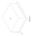
- FIG. 2illustrates an elevational view of an embodiment of a surface-mount power module formed with a discrete passive element constructed according to the principles of the present invention
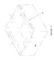
- FIG. 3illustrates an elevational view of another embodiment of a surface-mount power module formed with a discrete passive element constructed according to the principles of the present invention.
- FIGS. 4 to 8illustrate views of an embodiment of a power module at different stages of completion constructed according to the principles of the present invention.
- a power modulee.g., an electronic device
- a discrete or separate passive element and a semiconductor devicee.g., a discrete or separate passive element and a semiconductor device
- a method of manufacture therefore.g., a semiconductor device, and a method of manufacture therefor. While the principles of the present invention will be described in the environment of a power module, any application that may benefit from a semiconductor device mounted on a discrete passive element as described herein is well within the broad scope of the present invention.
- a discrete passive elementmay be embodied, without limitation, in an inductor or a transformer.
- a semiconductor devicemay include active elements (e.g., a switch) and passive elements (e.g., diodes, resistors, capacitors) and circuits such as controllers with control circuit elements such as operational amplifiers and comparators.
- active elementse.g., a switch
- passive elementse.g., diodes, resistors, capacitors
- circuitssuch as controllers with control circuit elements such as operational amplifiers and comparators.
- the broad scope of the present inventionis not limited to the particular elements that form the semiconductor device.
- the semiconductor devicemay include integrated circuits (either in bare die or in module form) coupled (e.g., adhesively mounted) to a conductive substrate (e.g., a leadframe), and electrically coupled thereto with wire bonds, as well as surface-mount elements coupled thereon.
- An encapsulantsuch as plastic molded material, for example, an epoxy material, is placed around the discrete passive element and the semiconductor device, and any additional elements to provide environmental and mechanical protection as well as a thermally conductive covering to facilitate heat dissipation during operation of the power module.
- Other molding materials and processes as well as electronic devices constructed without an encapsulantare well within the broad scope of the present invention.
- the power modulemay form, at least in part, a power management system, which itself is often referred to as a power management integrated circuit.
- FIG. 1illustrated is a schematic diagram of an embodiment of a power converter including power conversion circuitry employable in a power module constructed according to the principles of the present invention.
- the power converterincludes a power train 110 , a controller 120 and a driver 130 including control circuit elements, and provides power to a system such as a microprocessor. While in the illustrated embodiment, the power train 110 employs a buck converter topology, those skilled in the art should understand that other converter topologies such as a forward converter topology are well within the broad scope of the present invention.
- the power train 110receives an input voltage V in from a source of electrical power (represented by a battery) at an input thereof and provides a regulated output voltage V out to power, for instance, a microprocessor at an output thereof.
- the output voltage V outis generally less than the input voltage V in such that a switching operation of the power converter can regulate the output voltage V out .
- An active elementsuch as a switch (e.g., a main switch Q mn ) is enabled to conduct for a primary interval (generally co-existent with a primary duty cycle “D” of the main switch Q mn ) and couples the input voltage V in to an output filter inductor L out .
- an inductor current I Lout flowing through the output filter inductor L outincreases as a current flows from the input to the output of the power train 110 .
- a portion of the inductor current I Loutis filtered by the output capacitor C out .
- the main switch Q mnis transitioned to a non-conducting state and another active element such as another switch (e.g., an auxiliary switch Q aux ) is enabled to conduct.
- the auxiliary switch Q auxprovides a path to maintain a continuity of the inductor current I Lout flowing through the output filter inductor L out .
- the inductor current I Lout through the output filter inductor L outdecreases.
- the duty cycle of the main and auxiliary switches Q mn , Q auxmay be adjusted to maintain a regulation of the output voltage V out of the power converter.
- the conduction periods for the main and auxiliary switches Q mn , Q auxmay be separated by a small time interval to avoid cross conduction therebetween and beneficially to reduce the switching losses associated with the power converter.
- the controller 120receives a desired characteristic such as a desired system voltage V system from an internal or external source associated with the microprocessor, and the output voltage V out of the power converter.
- the controller 120is also coupled to the input voltage V in of the power converter and a return lead of the source of electrical power (again, represented by a battery) to provide a ground connection therefor.
- a decoupling capacitor C decis coupled to the path from the input voltage V in to the controller 120 .
- the decoupling capacitor C decis configured to absorb high frequency noise signals associated with the source of electrical power to protect the controller 120 .
- the controller 120provides a signal (e.g., a pulse width modulated signal S PWM ) to control a duty cycle and a frequency of the main and auxiliary switches Q mn , Q aux of the power train 110 to regulate the output voltage V out thereof.
- the controller 120may also provide a complement of the signal (e.g., a complementary pulse width modulated signal S 1-PWM ) in accordance with the aforementioned characteristics.
- Any controller adapted to control at least one switch of the power converteris well within the broad scope of the present invention.
- a controller employing digital circuitryis disclosed in U.S. Pat. No.
- the power converteralso includes the driver 130 configured to provide drive signals S DRV1 , S DRV2 to the main and auxiliary switches Q mn , Q aux , respectively, based on the signals S PWM , S 1-PWM provided by the controller 120 .
- the driver 130typically includes active elements such as switching circuitry incorporating a plurality of driver switches that cooperate to provide the drive signals S DRV1 , S DRV2 to the main and auxiliary switches Q mn , Q aux .
- any driver 130capable of providing the drive signals S DRV1 , S DRV2 to control a switch is well within the broad scope of the present invention.
- a driveris disclosed in U.S. Pat. No. 7,330,017, entitled “Driver for a Power Converter and Method of Driving a Switch Thereof,” to Dwarakanath, et al., which is incorporated herein by reference.
- an embodiment of a semiconductor device that may embody portions of the power conversion circuitryis disclosed in U.S. Pat. No.
- FIG. 2illustrated is an elevational view of an embodiment of a surface-mount power module formed with a discrete passive element, such as an inductor soldered to a leadframe 201 , constructed according to the principles of the present invention.
- the discrete passive elementincludes a main body 203 that may be formed with a ceramic material with metallic ends 202 thereof.
- the metallic ends 202 of the main body 203 of the discrete passive elementare generally tinned to enable surface-mount soldering to the leadframe 201 .
- the discrete passive elementmay include a magnetic device such as an inductor formed with an electrically conductive loop 204 embedded in a magnetic material such as a soft ferrite to form the main body 203 .
- a top surface of the metallic ends 202 of the main body 203are generally slightly elevated from the top surface of a central portion of the main body 203 of the discrete passive element.
- the leadframe 201may be formed as a patterned, conductive area of a metallic sheet such as copper foil, or as the etched upper surface of a printed wiring board, thereby forming a substrate.
- a typical thickness of the leadframe 201is about eight mils. While the leadframe 201 is often constructed of copper, alternative electrically conductive materials can be used therefor.
- the leadframe 201may provide external connections within and external to the power module as well as a support base for the discrete passive element.
- Solder pasteis selectively applied or disposed to the leadframe 201 in a thin layer to areas (e.g., a pad of the leadframe 201 ) for screening processes to provide electrical and mechanical attachment for surface-mount elements such as the discrete passive element.
- the surface-mount elementssuch as capacitors may be placed with their conductive ends in the solder paste.
- the solder pastemay be composed of lead-based as well as lead-free compositions.
- a thermally conductive and electrically insulating material 205is dispensed thereon to form an upper planar surface that acts as a die-attach layer for a semiconductor device 206 that is adhesively bonded thereon.
- An exemplary thermally conductive and electrically insulating material 205is epoxy. The adhesive is cured, typically in a controlled thermal process, to secure the semiconductor device to the discrete passive element.
- An exemplary thermally conductive and electrically insulating material 205 used to mount the semiconductor device 206 on to the discrete passive elementis Ablebond 2025D from Ablestik, Collinso Dominguez, Calif.
- the thermally conductive and electrically insulating material 205is dispensed (applied) on to the discrete passive element and the semiconductor device 206 is pressed into the thermally conductive and electrically insulating material 205 forcing spreading of the same under the semiconductor device 206 to obtain a minimum of 75% coverage of the bottom surface semiconductor device 206 .
- a curing process in an in-line oven for up to about 45 minutes at about 175 degrees Celsiusis used to cure the thermally conductive and electrically insulating material 205 .
- the semiconductor device 206is electrically coupled to the patterned leadframe 201 by wire bonds (not shown).
- the assemblyis then encapsulated in a molded package 207 , preferably by a thermo-setting encapsulant material such as an epoxy molding compound from Sumikon EME-G770LC from Sumitomo Bakelite, Tokyo, Japan by a transfer molding process to form a surface-mount power module.
- a thermo-setting encapsulant materialsuch as an epoxy molding compound from Sumikon EME-G770LC from Sumitomo Bakelite, Tokyo, Japan
- Electrical connections to an external circuitare made to the power module by electrically conductive pads formed about the edges of the power module as illustrated and described with reference to FIGS. 4 and 5 .
- electrical connectionsare made to the power module by electrically conductive pads (not shown) formed on the lower surface of the power module.
- the power modulemay be electrically bonded to an external circuit such as a another circuit board or printed wiring board using reflow solder techniques in a reflow oven, as is well understood in the art.
- the power modulemay be formed as a through-hole mounted power module employing leads that extend from an outer surface of the power module such as from a side thereof.
- heat produced in the semiconductor deviceis conducted through the thermally conductive layer 205 to the discrete passive element (e.g., through the metallic ends 202 of the main body 203 ), from which the heat is conducted to the leadframe 201 , and then out of the power module.
- Heat flowis enhanced by the presence of the metallic ends 202 of the discrete passive element, recognizing the generally high thermal conductivity of metallic structures.
- the metallic ends 202 of the discrete passive elementmay be tinned as conventionally formed with a base layer of silver, a supplementary base layer of copper, an intermetallic barrier layer of nickel, followed by a solderable surface of tin.
- FIG. 3illustrated is an elevational view of an embodiment of a surface-mount power module formed with an extended metallic region 302 of a main body 203 of a discrete passive element constructed according to the principles of the present invention.
- the extended metallic region 302which may also be tinned, extends from one of the metallic ends 202 and enhances the thermal conductivity of the heat flow path from a semiconductor device to the leadframe 201 , and then to the external environment of the power module.
- a high heat-producing region 306 of the semiconductor devicesuch as a field-effect transistor, is located above the extended metallic region 302 .
- a lower heat-producing region 308 of the semiconductor devicemay be located above a remaining portion of the main body 203 of the discrete passive element. The remaining elements of the power module of FIG. 3 previously introduced will not be redescribed in the interest of brevity.
- FIGS. 4 to 8illustrated are views of an embodiment of a power module at different stages of completion constructed according to the principles of the present invention.
- a leadframe 405that provides the foundation for the power module.
- the leadframe 405includes a pad 410 that provides a base for a discrete passive element and leads (one of which is designated 415 ) that provides electrical connections for a semiconductor device located above the discrete passive element.
- FIG. 5illustrated is an isometric view of an embodiment of the power module with the discrete passive element and semiconductor device constructed on the leadframe 405 of the power module.
- the discrete passive elementincludes a main body 420 with a generally planar upper surface and metallic ends 425 and is coupled to the pad 410 of the leadframe 405 via solder paste 417 , which is formed on the pad 410 prior to placing the discrete passive element thereon.
- a thermally conductive, electrically insulating layer 430formed with a planar upper surface.
- the semiconductor device formed as an unpackaged semiconductor dieincludes switches (e.g., metal-oxide semiconductor field-effect transistors) 435 and a controller 440 and is bonded to the upper surface of the thermally conductive, electrically insulating layer 430 .
- Pads, such as pad 445 , on an upper surface of the semiconductor deviceare coupled by wire bonds, such as wire bond 450 , to the electrically conductive leads 415 formed on the leadframe 405 .
- the wire bonds 450are preferably formed of gold wire to provide electrical circuit connections between the pads 445 on the upper surface of the semiconductor device and the electrically conductive leads 415 formed on the leadframe 405 .
- Thermal conductivity of the heat path from the semiconductor device through the thermally conductive, electrically insulating layer 430is enhanced by an overlapping region 455 of the semiconductor device with the metallic ends 425 of the main body 420 of the discrete passive element.
- high heat dissipating portions of the semiconductor deviceare located over or near an overlapping region such as overlapping region 455 .
- steps as described above to form a power modulegenerally do not require execution in the highly controlled environment of a clean room. Some steps, however, may be preferably performed in a clean room or other controlled environment such as typically used for assembly of integrated circuits into a molded plastic package, as is generally well known in the art.
- FIG. 6illustrated is an isometric view of an embodiment of the power module after encapsulation by transfer molding with an encapsulant 460 such as an epoxy material constructed according to the principles of the present invention.
- an encapsulant 460such as an epoxy material constructed according to the principles of the present invention.
- the ends of the leadframe 405are exposed about the encapsulant 460 with the electrically conductive leads (not shown) for contact to another circuit board, printed wiring board, substrate or the like.
- FIGS. 7 and 8illustrated are isometric views of an embodiment of the power module after the ends of the leadframe (not shown) have been removed (such as by sawing) in accordance with the principles of the present invention.
- the electrically conductive leads or contacts 415are disposed along the outer edges (see FIG. 7 ) and lower edges (see FIG. 8 ) of the power module to enable the power module to be reflow soldered to a printed wiring board in an end product.
- the electrically conductive leads or contacts 415are substantially coplanar with the sides and lower surface of the power module and provide electrical connectivity to an external circuit.
- Electrical connections of the power module to the system employing the power moduleare made by placing the power module on another circuit board or printed wiring board formed with interconnect pads that are covered with solder paste, generally by a screening operation, and heating the power module on the circuit board in a reflow oven.
- the reflow soldering operationis generally adequate to provide mechanical attachment of the power module to another circuit board, but other attachment methods such as adhesive compound are well within the broad scope of the present invention.
- the exemplary lateral dimensions of the power module as illustrated in FIGS. 4 to 8are 2.5 millimeters (“mm”) ⁇ 2.25 mm.
- the height of the moduleis 1.1 mm.
- a power module of these dimensionscan produce an output current of 1 amperes at 3.3 volts, resulting in a power conversion density of 0.53 watts/cubic-mm (“W/mm 3 ”).
- W/mm 3power conversion density
- the broad scope of the present inventionis not limited to a power module, power converter or the like, having the aforementioned dimensions and ratings, and may be applicable to other electronic devices as well.
Landscapes
- Engineering & Computer Science (AREA)
- Microelectronics & Electronic Packaging (AREA)
- Power Engineering (AREA)
- Computer Hardware Design (AREA)
- Physics & Mathematics (AREA)
- Condensed Matter Physics & Semiconductors (AREA)
- General Physics & Mathematics (AREA)
- Dc-Dc Converters (AREA)
Abstract
Description
Claims (20)
Priority Applications (2)
| Application Number | Priority Date | Filing Date | Title |
|---|---|---|---|
| US12/244,672US8153473B2 (en) | 2008-10-02 | 2008-10-02 | Module having a stacked passive element and method of forming the same |
| US12/393,835US8266793B2 (en) | 2008-10-02 | 2009-02-26 | Module having a stacked magnetic device and semiconductor device and method of forming the same |
Applications Claiming Priority (1)
| Application Number | Priority Date | Filing Date | Title |
|---|---|---|---|
| US12/244,672US8153473B2 (en) | 2008-10-02 | 2008-10-02 | Module having a stacked passive element and method of forming the same |
Related Child Applications (1)
| Application Number | Title | Priority Date | Filing Date |
|---|---|---|---|
| US12/393,835Continuation-In-PartUS8266793B2 (en) | 2008-10-02 | 2009-02-26 | Module having a stacked magnetic device and semiconductor device and method of forming the same |
Publications (2)
| Publication Number | Publication Date |
|---|---|
| US20100087036A1 US20100087036A1 (en) | 2010-04-08 |
| US8153473B2true US8153473B2 (en) | 2012-04-10 |
Family
ID=42076120
Family Applications (1)
| Application Number | Title | Priority Date | Filing Date |
|---|---|---|---|
| US12/244,672Expired - Fee RelatedUS8153473B2 (en) | 2008-10-02 | 2008-10-02 | Module having a stacked passive element and method of forming the same |
Country Status (1)
| Country | Link |
|---|---|
| US (1) | US8153473B2 (en) |
Cited By (10)
| Publication number | Priority date | Publication date | Assignee | Title |
|---|---|---|---|---|
| US20080303125A1 (en)* | 2007-06-08 | 2008-12-11 | Da-Jung Chen | Three-dimensional package structure |
| US20110134613A1 (en)* | 2009-12-07 | 2011-06-09 | Intersil Americas Inc. | Stacked inductor-electronic package assembly and technique for manufacturing same |
| US20130001756A1 (en)* | 2007-06-08 | 2013-01-03 | Cyntec Co., Ltd. | Three-dimensional package structure |
| US8618900B2 (en) | 2007-09-10 | 2013-12-31 | Enpirion, Inc. | Micromagnetic device and method of forming the same |
| US20140152350A1 (en)* | 2012-12-05 | 2014-06-05 | Volterra Semiconductor Corporation | Integrated Circuits Including Magnetic Devices, And Associated Methods |
| US9054086B2 (en) | 2008-10-02 | 2015-06-09 | Enpirion, Inc. | Module having a stacked passive element and method of forming the same |
| US9263177B1 (en) | 2012-03-19 | 2016-02-16 | Volterra Semiconductor LLC | Pin inductors and associated systems and methods |
| US9673135B2 (en) | 2014-01-13 | 2017-06-06 | Altera Corporation | Semiconductor device having mirror-symmetric terminals and methods of forming the same |
| US10314159B2 (en)* | 2015-12-18 | 2019-06-04 | Lg Chem, Ltd. | Printed circuit board heat dissipation system using highly conductive heat dissipation pad |
| US11317545B1 (en) | 2020-10-26 | 2022-04-26 | Modular Power Technology, Inc. | Apparatus for an inductor disposed in a band for method of heat dispersion |
Families Citing this family (26)
| Publication number | Priority date | Publication date | Assignee | Title |
|---|---|---|---|---|
| US7462317B2 (en) | 2004-11-10 | 2008-12-09 | Enpirion, Inc. | Method of manufacturing an encapsulated package for a magnetic device |
| US7426780B2 (en) | 2004-11-10 | 2008-09-23 | Enpirion, Inc. | Method of manufacturing a power module |
| US8631560B2 (en)* | 2005-10-05 | 2014-01-21 | Enpirion, Inc. | Method of forming a magnetic device having a conductive clip |
| US8139362B2 (en)* | 2005-10-05 | 2012-03-20 | Enpirion, Inc. | Power module with a magnetic device having a conductive clip |
| US7688172B2 (en)* | 2005-10-05 | 2010-03-30 | Enpirion, Inc. | Magnetic device having a conductive clip |
| US8701272B2 (en) | 2005-10-05 | 2014-04-22 | Enpirion, Inc. | Method of forming a power module with a magnetic device having a conductive clip |
| US8018315B2 (en)* | 2007-09-10 | 2011-09-13 | Enpirion, Inc. | Power converter employing a micromagnetic device |
| US8133529B2 (en)* | 2007-09-10 | 2012-03-13 | Enpirion, Inc. | Method of forming a micromagnetic device |
| US7952459B2 (en)* | 2007-09-10 | 2011-05-31 | Enpirion, Inc. | Micromagnetic device and method of forming the same |
| US7955868B2 (en)* | 2007-09-10 | 2011-06-07 | Enpirion, Inc. | Method of forming a micromagnetic device |
| US8692532B2 (en) | 2008-04-16 | 2014-04-08 | Enpirion, Inc. | Power converter with controller operable in selected modes of operation |
| US8541991B2 (en) | 2008-04-16 | 2013-09-24 | Enpirion, Inc. | Power converter with controller operable in selected modes of operation |
| US8686698B2 (en) | 2008-04-16 | 2014-04-01 | Enpirion, Inc. | Power converter with controller operable in selected modes of operation |
| US9246390B2 (en) | 2008-04-16 | 2016-01-26 | Enpirion, Inc. | Power converter with controller operable in selected modes of operation |
| US8339802B2 (en)* | 2008-10-02 | 2012-12-25 | Enpirion, Inc. | Module having a stacked magnetic device and semiconductor device and method of forming the same |
| US9548714B2 (en)* | 2008-12-29 | 2017-01-17 | Altera Corporation | Power converter with a dynamically configurable controller and output filter |
| US8698463B2 (en)* | 2008-12-29 | 2014-04-15 | Enpirion, Inc. | Power converter with a dynamically configurable controller based on a power conversion mode |
| US8867295B2 (en) | 2010-12-17 | 2014-10-21 | Enpirion, Inc. | Power converter for a memory module |
| US20140159130A1 (en) | 2012-11-30 | 2014-06-12 | Enpirion, Inc. | Apparatus including a semiconductor device coupled to a decoupling device |
| US9936579B2 (en) | 2013-02-01 | 2018-04-03 | Apple Inc. | Low profile packaging and assembly of a power conversion system in modular form |
| US9859250B2 (en)* | 2013-12-20 | 2018-01-02 | Cyntec Co., Ltd. | Substrate and the method to fabricate thereof |
| US20150200156A1 (en)* | 2014-01-13 | 2015-07-16 | Altera Corporation | Module having mirror-symmetric terminals and methods of forming the same |
| US9509217B2 (en) | 2015-04-20 | 2016-11-29 | Altera Corporation | Asymmetric power flow controller for a power converter and method of operating the same |
| US12058814B2 (en)* | 2016-03-03 | 2024-08-06 | Delta Electronics (Shanghai) Co., Ltd. | Power module and manufacturing method thereof |
| JP7542390B2 (en)* | 2020-10-08 | 2024-08-30 | 株式会社東芝 | Electrical equipment and power conversion devices |
| US11853088B2 (en)* | 2021-09-08 | 2023-12-26 | International Business Machines Corporation | Linking separate eFuse and ORING controllers for output overvoltage protection in redundant power converters |
Citations (160)
| Publication number | Priority date | Publication date | Assignee | Title |
|---|---|---|---|---|
| US1889398A (en) | 1932-03-05 | 1932-11-29 | Western Electric Co | Electrical coil and a method of manufacturing it |
| US2600473A (en) | 1949-01-26 | 1952-06-17 | Philips Lab Inc | Magnetic core |
| US3210707A (en) | 1962-10-04 | 1965-10-05 | Gen Instrument Corp | Solid state inductor built up of multiple thin films |
| US3691497A (en) | 1970-10-15 | 1972-09-12 | Us Army | Leadless microminiature inductance element with a closed magnetic circuit |
| US3762039A (en) | 1971-09-10 | 1973-10-02 | Mos Technology Inc | Plastic encapsulation of microcircuits |
| US3902148A (en) | 1970-11-27 | 1975-08-26 | Signetics Corp | Semiconductor lead structure and assembly and method for fabricating same |
| US3908264A (en) | 1974-04-24 | 1975-09-30 | Gen Instrument Corp | Method for calibrating a resonant frequency |
| US3947699A (en) | 1974-08-29 | 1976-03-30 | Iowa State University Research Foundation, Inc. | Apparatus for selecting a predetermined portion of an analog signal and gating it to an output |
| US4101389A (en) | 1976-05-20 | 1978-07-18 | Sony Corporation | Method of manufacturing amorphous alloy |
| US4103267A (en) | 1977-06-13 | 1978-07-25 | Burr-Brown Research Corporation | Hybrid transformer device |
| US4187128A (en) | 1978-09-26 | 1980-02-05 | Bell Telephone Laboratories, Incorporated | Magnetic devices including amorphous alloys |
| US4199743A (en) | 1978-02-06 | 1980-04-22 | Westinghouse Electric Corp. | Encapsulated current transformer |
| GB2041818A (en) | 1979-02-10 | 1980-09-17 | Plessey Co Ltd | Encapsulating a Magnetic Domain Component |
| US4433927A (en) | 1981-02-25 | 1984-02-28 | Honeywell Information Systems Italia | Electromagnet assembly for mosaic printing head and related manufacturing method |
| US4586436A (en) | 1984-09-13 | 1986-05-06 | The United States Of America As Represented By The Secretary Of The Navy | Electronic assembly for moderate hard target penetrator fuze |
| US4636752A (en) | 1984-06-08 | 1987-01-13 | Murata Manufacturing Co., Ltd. | Noise filter |
| US4668310A (en) | 1979-09-21 | 1987-05-26 | Hitachi Metals, Ltd. | Amorphous alloys |
| US4681718A (en) | 1984-05-09 | 1987-07-21 | Hughes Aircraft Company | Method of fabricating composite or encapsulated articles |
| US4751199A (en) | 1983-12-06 | 1988-06-14 | Fairchild Semiconductor Corporation | Process of forming a compliant lead frame for array-type semiconductor packages |
| US4754317A (en) | 1986-04-28 | 1988-06-28 | Monolithic Memories, Inc. | Integrated circuit die-to-lead frame interconnection assembly and method |
| US4777465A (en) | 1986-04-28 | 1988-10-11 | Burr-Brown Corporation | Square toroid transformer for hybrid integrated circuit |
| US4808118A (en) | 1987-11-25 | 1989-02-28 | Itt Corporation | Retention and ground plane connector clip |
| US4870224A (en) | 1988-07-01 | 1989-09-26 | Intel Corporation | Integrated circuit package for surface mount technology |
| US4916522A (en) | 1988-04-21 | 1990-04-10 | American Telephone And Telegraph Company , At & T Bell Laboratories | Integrated circuit package using plastic encapsulant |
| US4975671A (en) | 1988-08-31 | 1990-12-04 | Apple Computer, Inc. | Transformer for use with surface mounting technology |
| US5056214A (en) | 1989-12-19 | 1991-10-15 | Mark Iv Industries, Inc | Method of making a molded transformer enclosure |
| US5059278A (en) | 1990-09-28 | 1991-10-22 | Seagate Technology | Selective chemical removal of coil seed-layer in thin film head magnetic transducer |
| US5096513A (en) | 1989-09-01 | 1992-03-17 | Kabushiki Kaisha Toshiba | Very thin soft magnetic alloy strips and magnetic core and electromagnetic apparatus made therefrom |
| US5118298A (en) | 1991-04-04 | 1992-06-02 | Advanced Interconnections Corporation | Through hole mounting of integrated circuit adapter leads |
| US5161098A (en) | 1991-09-09 | 1992-11-03 | Power Integrations, Inc. | High frequency switched mode converter |
| US5187119A (en) | 1991-02-11 | 1993-02-16 | The Boeing Company | Multichip module and integrated circuit substrates having planarized patterned surfaces |
| US5262296A (en) | 1988-03-30 | 1993-11-16 | Toray Industries, Inc. | Freeze-dried composition containing enzyme-labeled anti-human interferon-β antibody and enzyme immunoassay kit containing the composition |
| US5279988A (en) | 1992-03-31 | 1994-01-18 | Irfan Saadat | Process for making microcomponents integrated circuits |
| US5285369A (en) | 1992-09-01 | 1994-02-08 | Power Integrations, Inc. | Switched mode power supply integrated circuit with start-up self-biasing |
| US5345670A (en) | 1992-12-11 | 1994-09-13 | At&T Bell Laboratories | Method of making a surface-mount power magnetic device |
| US5353001A (en) | 1991-01-24 | 1994-10-04 | Burr-Brown Corporation | Hybrid integrated circuit planar transformer |
| US5428245A (en) | 1994-05-06 | 1995-06-27 | National Semiconductor Corporation | Lead frame including an inductor or other such magnetic component |
| US5436409A (en) | 1991-01-10 | 1995-07-25 | Sumitomo Electric Industries, Ltd. | Electrical conductor member such as a wire with an inorganic insulating coating |
| US5469334A (en) | 1991-09-09 | 1995-11-21 | Power Integrations, Inc. | Plastic quad-packaged switched-mode integrated circuit with integrated transformer windings and mouldings for transformer core pieces |
| US5484494A (en) | 1992-05-14 | 1996-01-16 | Mitsubishi Rayon Company, Inc. | Amorphous alloy and method for its production |
| US5524334A (en) | 1990-03-13 | 1996-06-11 | Boesel; Robert P. | Method of making an encapsulated high efficiency transformer and power supply |
| US5561438A (en) | 1991-11-13 | 1996-10-01 | Seiko Epson Corporation | Ferrite Antenna |
| US5574420A (en) | 1994-05-27 | 1996-11-12 | Lucent Technologies Inc. | Low profile surface mounted magnetic devices and components therefor |
| US5574273A (en) | 1993-06-14 | 1996-11-12 | Hitachi Maxell, Ltd. | Non-contact system parallel data transfer system |
| US5578261A (en) | 1993-05-17 | 1996-11-26 | Lucent Technologies Inc. | Method of encapsulating large substrate devices using reservoir cavities for balanced mold filling |
| US5692296A (en) | 1993-08-18 | 1997-12-02 | Lsi Logic Corporation | Method for encapsulating an integrated circuit package |
| US5783025A (en) | 1994-06-07 | 1998-07-21 | Texas Instruments Incorporated | Optical diebonding for semiconductor devices |
| US5788854A (en) | 1993-08-16 | 1998-08-04 | California Micro Devices Corporation | Methods for fabrication of thin film inductors, inductor networks, inductor/capactor filters, and integration with other passive and active devices, and the resultant devices |
| US5787569A (en) | 1996-02-21 | 1998-08-04 | Lucent Technologies Inc. | Encapsulated package for power magnetic devices and method of manufacture therefor |
| US5802702A (en) | 1994-06-30 | 1998-09-08 | Lucent Technologies Inc. | Method of making a device including a metallized magnetic substrate |
| US5807959A (en) | 1995-12-21 | 1998-09-15 | National Starch And Chemical Investment Holding Corporation | Flexible epoxy adhesives with low bleeding tendency |
| US5834691A (en) | 1995-01-19 | 1998-11-10 | Sharp Kabushiki Kaisha | Lead frame, its use in the fabrication of resin-encapsulated semiconductor device |
| US5835350A (en) | 1996-12-23 | 1998-11-10 | Lucent Technologies Inc. | Encapsulated, board-mountable power supply and method of manufacture therefor |
| US5837155A (en) | 1995-08-28 | 1998-11-17 | Taiyo Ink Manufacturing Co., Ltd. | Insulating resin composition for build-up by copper foil lamination and method for production of multilayer printed circuit board using the composition |
| US5846441A (en) | 1995-09-30 | 1998-12-08 | Daewoo Electronics Co., Ltd. | Method for forming a patterned metallic layer in a thin film magnetic head |
| US5898991A (en) | 1997-01-16 | 1999-05-04 | International Business Machines Corporation | Methods of fabrication of coaxial vias and magnetic devices |
| US5920249A (en) | 1997-10-30 | 1999-07-06 | Ford Motor Company | Protective method of support for an electromagnetic apparatus |
| US5973923A (en) | 1998-05-28 | 1999-10-26 | Jitaru; Ionel | Packaging power converters |
| US5998925A (en) | 1996-07-29 | 1999-12-07 | Nichia Kagaku Kogyo Kabushiki Kaisha | Light emitting device having a nitride compound semiconductor and a phosphor containing a garnet fluorescent material |
| US6005467A (en) | 1997-02-11 | 1999-12-21 | Pulse Engineering, Inc. | Trimmable inductor |
| US6005377A (en) | 1997-09-17 | 1999-12-21 | Lucent Technologies Inc. | Programmable digital controller for switch mode power conversion and power supply employing the same |
| US6060176A (en) | 1995-11-30 | 2000-05-09 | International Business Machines Corporation | Corrosion protection for metallic features |
| US6081997A (en) | 1997-08-14 | 2000-07-04 | Lsi Logic Corporation | System and method for packaging an integrated circuit using encapsulant injection |
| US6087920A (en) | 1997-02-11 | 2000-07-11 | Pulse Engineering, Inc. | Monolithic inductor |
| US6087921A (en) | 1998-10-06 | 2000-07-11 | Pulse Engineering, Inc. | Placement insensitive monolithic inductor and method of manufacturing same |
| US6094123A (en) | 1998-09-25 | 2000-07-25 | Lucent Technologies Inc. | Low profile surface mount chip inductor |
| US6101218A (en) | 1994-06-27 | 2000-08-08 | Advantest Corp. | Leakage power measurement apparatus and method |
| US6118360A (en) | 1996-01-11 | 2000-09-12 | Systems, Machines, Automation Components Corporation | Linear actuator |
| US6118351A (en) | 1997-06-10 | 2000-09-12 | Lucent Technologies Inc. | Micromagnetic device for power processing applications and method of manufacture therefor |
| US6255714B1 (en) | 1999-06-22 | 2001-07-03 | Agere Systems Guardian Corporation | Integrated circuit having a micromagnetic device including a ferromagnetic core and method of manufacture therefor |
| US20010030595A1 (en) | 2000-03-14 | 2001-10-18 | Junichi Hamatani | Inductor and method for manufacturing same |
| US20010041384A1 (en) | 1998-05-12 | 2001-11-15 | Mitsubishi Denki Kabushiki Kaisha | Method of producing semiconductor device and configuration thereof, and lead frame used in said method |
| US6317948B1 (en) | 1997-08-25 | 2001-11-20 | Agere Systems Guardian Corp. | Embedded thin film passive components |
| US6353379B1 (en) | 2000-02-28 | 2002-03-05 | Lucent Technologies Inc. | Magnetic device employing a winding structure spanning multiple boards and method of manufacture thereof |
| US6366486B1 (en) | 2000-08-29 | 2002-04-02 | Delta Electronics Inc. | Power supply device for enhancing heat-dissipating effect |
| US6440750B1 (en) | 1997-06-10 | 2002-08-27 | Agere Systems Guardian Corporation | Method of making integrated circuit having a micromagnetic device |
| US6448640B2 (en) | 1999-09-02 | 2002-09-10 | Micron Technology, Inc. | Ball array layout in chip assembly |
| US6466454B1 (en) | 1999-05-18 | 2002-10-15 | Ascom Energy Systems Ag | Component transformer |
| US20020153258A1 (en) | 2000-04-19 | 2002-10-24 | Filas Robert W. | Device comprising micromagnetic components for power applications and process for forming device |
| US6479981B2 (en) | 1998-06-29 | 2002-11-12 | E.O. Schweitzer Manufacturing Co., Inc. | Remote light indication fault indicator with a timed reset circuit and a manual reset circuit |
| US6541819B2 (en) | 2001-05-24 | 2003-04-01 | Agere Systems Inc. | Semiconductor device having non-power enhanced and power enhanced metal oxide semiconductor devices and a method of manufacture therefor |
| US20030062541A1 (en) | 2001-08-28 | 2003-04-03 | Michael Warner | High-frequency chip packages |
| US6549409B1 (en) | 2000-08-21 | 2003-04-15 | Vlt Corporation | Power converter assembly |
| US6552629B2 (en) | 2000-12-12 | 2003-04-22 | Micrel, Incorporated | Universally stable output filter |
| US20030076662A1 (en) | 1999-05-14 | 2003-04-24 | Sokymat S.A. | Transponder and injection-molded part and method for manufacturing same |
| US6578253B1 (en) | 1991-10-04 | 2003-06-17 | Fmtt, Inc. | Transformer and inductor modules having directly bonded terminals and heat-sink fins |
| US6608332B2 (en) | 1996-07-29 | 2003-08-19 | Nichia Kagaku Kogyo Kabushiki Kaisha | Light emitting device and display |
| US20030232196A1 (en) | 2002-06-14 | 2003-12-18 | Krishnamurthy Anand | Coated ferromagnetic particles and composite magnetic articles thereof |
| US6691398B2 (en) | 1999-05-18 | 2004-02-17 | Pulse Engineering | Electronic packaging device and method |
| US6693805B1 (en) | 2002-07-31 | 2004-02-17 | Lockheed Martin Corporation | Ripple cancellation circuit for ultra-low-noise power supplies |
| US6731002B2 (en) | 2001-05-04 | 2004-05-04 | Ixys Corporation | High frequency power device with a plastic molded package and direct bonded substrate |
| US6747538B2 (en) | 2001-09-28 | 2004-06-08 | Matsushita Electric Industrial Co., Ltd. | Inductance device |
| US20040130428A1 (en) | 2002-10-31 | 2004-07-08 | Peter Mignano | Surface mount magnetic core winding structure |
| US20040150500A1 (en) | 2001-11-14 | 2004-08-05 | Kiko Frederick J. | Controlled induction device and method of manufacturing |
| US6790379B2 (en) | 1999-09-20 | 2004-09-14 | Tdk Corporation | Magnetic ferrite composition and process of production thereof |
| US20050011672A1 (en) | 2003-07-17 | 2005-01-20 | Alawani Ashish D. | Overmolded MCM with increased surface mount component reliability |
| US6912781B2 (en) | 2000-01-31 | 2005-07-05 | Pulse Engineering, Inc. | Method of manufacturing electronic packaging device with insertable leads |
| US6922130B2 (en) | 2002-05-24 | 2005-07-26 | Minebea Co., Ltd. | Surface mount coil with edgewise winding |
| US20050168205A1 (en) | 2004-01-29 | 2005-08-04 | Enpirion, Incorporated | Controller for a power converter and a method of controlling a switch thereof |
| US20050168203A1 (en) | 2004-01-29 | 2005-08-04 | Enpirion, Incorporated | Driver for a power converter and a method of driving a switch thereof |
| US20050167756A1 (en) | 2004-01-29 | 2005-08-04 | Enpirion, Incorporated | Laterally diffused metal oxide semiconductor device and method of forming the same |
| US20050169024A1 (en) | 2004-01-29 | 2005-08-04 | Enpirion, Incorporated, A Delaware Corporation | Controller for a power converter and a method of controlling a switch thereof |
| US20050212132A1 (en) | 2004-03-25 | 2005-09-29 | Min-Chih Hsuan | Chip package and process thereof |
| US20060009023A1 (en) | 2002-06-25 | 2006-01-12 | Unitive International Limited | Methods of forming electronic structures including conductive shunt layers and related structures |
| US6989121B2 (en) | 1998-02-05 | 2006-01-24 | Micron Technology, Inc. | Method for encasing plastic array packages |
| US6998952B2 (en) | 2003-12-05 | 2006-02-14 | Freescale Semiconductor, Inc. | Inductive device including bond wires |
| US20060040449A1 (en) | 2004-08-23 | 2006-02-23 | Lotfi Ashraf W | Method of forming an integrated circuit incorporating higher voltage devices and low voltage devices therein |
| US20060040452A1 (en) | 2004-08-23 | 2006-02-23 | Lotfi Ashraf W | Method of forming an integrated circuit incorporating higher voltage devices and low voltage devices therein |
| US20060038225A1 (en) | 2004-08-23 | 2006-02-23 | Lotfi Ashraf W | Integrated circuit employable with a power converter |
| US7020295B2 (en) | 2001-07-11 | 2006-03-28 | Murata Manufacturing Co., Ltd. | Piezoelectric electroacoustic transducer and manufacturing method of the same |
| US7023315B2 (en) | 2000-04-24 | 2006-04-04 | Chartered Semiconductor Manufacturing Ltd. | High performance RF inductors and transformers using bonding technique |
| US20060097833A1 (en) | 2004-11-10 | 2006-05-11 | Lotfi Ashraf W | Encapsulated package for a magnetic device |
| US20060097831A1 (en) | 2004-11-10 | 2006-05-11 | Lotfi Ashraf W | Power module |
| US20060097832A1 (en) | 2004-11-10 | 2006-05-11 | Lotfi Ashraf W | Encapsulated package for a magnetic device |
| US20060096088A1 (en) | 2004-11-10 | 2006-05-11 | Lotfi Ashraf W | Method of manufacturing an encapsulated package for a magnetic device |
| US20060096087A1 (en) | 2004-11-10 | 2006-05-11 | Lotfi Ashraf W | Method of manufacturing a power module |
| US20060109072A1 (en) | 2002-05-31 | 2006-05-25 | International Rectifier Corporation | Planar transformer arrangement |
| US20060145800A1 (en) | 2004-08-31 | 2006-07-06 | Majid Dadafshar | Precision inductive devices and methods |
| US7101737B2 (en) | 2000-08-28 | 2006-09-05 | Micron Technology, Inc. | Method of encapsulating interconnecting units in packaged microelectronic devices |
| US20060197207A1 (en) | 2005-02-22 | 2006-09-07 | Stats Chippac Ltd. | Integrated circuit package system with die and package combination |
| US20070025092A1 (en) | 2005-08-01 | 2007-02-01 | Baik-Woo Lee | Embedded actives and discrete passives in a cavity within build-up layers |
| US7175718B2 (en) | 2001-06-19 | 2007-02-13 | Mitsubishi Denki Kabushiki Kaisha | Rare earth element permanent magnet material |
| US20070074386A1 (en) | 2005-10-05 | 2007-04-05 | Lotfi Ashraf W | Method of forming a power module with a magnetic device having a conductive clip |
| US20070075815A1 (en) | 2005-10-05 | 2007-04-05 | Lotfi Ashraf W | Method of forming a magnetic device having a conductive clip |
| US20070075816A1 (en) | 2005-10-05 | 2007-04-05 | Lotfi Ashraf W | Power module with a magnetic device having a conductive clip |
| US20070075817A1 (en) | 2005-10-05 | 2007-04-05 | Lotfi Ashraf W | Magnetic device having a conductive clip |
| US7214985B2 (en) | 2004-08-23 | 2007-05-08 | Enpirion, Inc. | Integrated circuit incorporating higher voltage devices and low voltage devices therein |
| US7230316B2 (en)* | 2002-12-27 | 2007-06-12 | Semiconductor Energy Laboratory Co., Ltd. | Semiconductor device having transferred integrated circuit |
| US7236086B1 (en) | 1993-06-14 | 2007-06-26 | Vlt, Inc. | Power converter configuration, control, and construction |
| US7250842B1 (en) | 2005-08-09 | 2007-07-31 | National Semiconductor Corporation | MEMS inductor with very low resistance |
| US20070210777A1 (en) | 2006-03-06 | 2007-09-13 | Cervera Pedro A | Controller for a power converter and method of operating the same |
| US20070246808A1 (en) | 2005-03-16 | 2007-10-25 | Henrik Ewe | Power semiconductor module having surface-mountable flat external contacts and method for producing the same |
| US20080001701A1 (en) | 2006-06-30 | 2008-01-03 | Gardner Donald S | Control of eddy currents in magnetic vias for inductors and transformers in integrated circuits |
| US20080090079A1 (en) | 2006-09-28 | 2008-04-17 | Fajardo Arnel M | High-resistivity magnetic film from nano-particle plating |
| US20080180075A1 (en) | 2007-01-29 | 2008-07-31 | Linear Technology Corporation | Current source with indirect load current signal extraction |
| US7434306B2 (en) | 1999-11-23 | 2008-10-14 | Intel Corporation | Integrated transformer |
| US20080258274A1 (en)* | 2005-01-20 | 2008-10-23 | Infineon Technologies Ag | Semiconductor Package and Method |
| US20080258278A1 (en) | 2002-04-29 | 2008-10-23 | Mary Jean Ramos | Partially patterned lead frames and methods of making and using the same in semiconductor packaging |
| US20080303131A1 (en) | 2007-06-11 | 2008-12-11 | Vertical Circuits, Inc. | Electrically interconnected stacked die assemblies |
| US20090004774A1 (en)* | 2007-06-27 | 2009-01-01 | Ming Hsun Lee | Method of multi-chip packaging in a tsop package |
| US7498522B2 (en) | 2006-01-30 | 2009-03-03 | Fujitsu Limited | Multilayer printed circuit board and manufacturing method thereof |
| US20090057822A1 (en)* | 2007-09-05 | 2009-03-05 | Yenting Wen | Semiconductor component and method of manufacture |
| US20090066467A1 (en) | 2007-09-10 | 2009-03-12 | Lotfi Ashraf W | Micromagnetic Device and Method of Forming the Same |
| US20090068347A1 (en) | 2007-09-10 | 2009-03-12 | Lotfi Ashraf W | Method of Forming a Micromagnetic Device |
| US20090066468A1 (en) | 2007-09-10 | 2009-03-12 | Lotfi Ashraf W | Power Converter Employing a Micromagnetic Device |
| US20090068761A1 (en) | 2007-09-10 | 2009-03-12 | Lotfi Ashraf W | Method of Forming a Micromagnetic Device |
| US20090066300A1 (en) | 2007-09-10 | 2009-03-12 | Lotfi Ashraf W | Power Converter Employing a Micromagnetic Device |
| US20090068400A1 (en) | 2007-09-10 | 2009-03-12 | Lotfi Ashraf W | Micromagnetic Device and Method of Forming the Same |
| US20090146297A1 (en) | 2007-12-06 | 2009-06-11 | Stats Chippac, Ltd. | Semiconductor Device and Method of Forming Wafer Level Ground Plane and Power Ring |
| US20100084750A1 (en) | 2008-10-02 | 2010-04-08 | Lotfi Ashraf W | Module having a stacked passive element and method of forming the same |
| US20100164449A1 (en) | 2008-12-29 | 2010-07-01 | Mirmira Ramarao Dwarakanath | Power Converter with a Dynamically Configurable Controller and Output Filter |
| US20100164650A1 (en) | 2008-12-29 | 2010-07-01 | Ahmed Mohamed Abou-Alfotouh | Power Converter with a Dynamically Configurable Controller and Output Filter |
| US20100212150A1 (en) | 2008-10-02 | 2010-08-26 | Lotfi Ashraf W | Module Having a Stacked Magnetic Device and Semiconductor Device and Method of Forming the Same |
| US20100214746A1 (en) | 2008-10-02 | 2010-08-26 | Lotfi Ashraf W | Module Having a Stacked Magnetic Device and Semiconductor Device and Method of Forming the Same |
| US7786837B2 (en)* | 2007-06-12 | 2010-08-31 | Alpha And Omega Semiconductor Incorporated | Semiconductor power device having a stacked discrete inductor structure |
| US7791440B2 (en) | 2004-06-09 | 2010-09-07 | Agency For Science, Technology And Research | Microfabricated system for magnetic field generation and focusing |
| US7876572B2 (en) | 2006-01-27 | 2011-01-25 | Sharp Kabushiki Kaisha | Wiring board and semiconductor apparatus |
| US7936160B1 (en) | 2007-04-25 | 2011-05-03 | National Semiconductor Corporation | Apparatus and method for valley emulated current mode control |
| US7948772B2 (en) | 2006-07-04 | 2011-05-24 | Orient Semiconductor Electronics | Memory card with electrostatic discharge protection and manufacturing method thereof |
| US7974103B2 (en) | 2006-09-13 | 2011-07-05 | Samsung Electronics Co., Ltd. | LCD signal transfer members |
Family Cites Families (2)
| Publication number | Priority date | Publication date | Assignee | Title |
|---|---|---|---|---|
| US701950A (en)* | 1901-09-12 | 1902-06-10 | Matt Shew | Cultivator. |
| TWI242506B (en)* | 2003-12-30 | 2005-11-01 | Ind Tech Res Inst | Automatic gear device |
- 2008
- 2008-10-02USUS12/244,672patent/US8153473B2/ennot_activeExpired - Fee Related
Patent Citations (189)
| Publication number | Priority date | Publication date | Assignee | Title |
|---|---|---|---|---|
| US1889398A (en) | 1932-03-05 | 1932-11-29 | Western Electric Co | Electrical coil and a method of manufacturing it |
| US2600473A (en) | 1949-01-26 | 1952-06-17 | Philips Lab Inc | Magnetic core |
| US3210707A (en) | 1962-10-04 | 1965-10-05 | Gen Instrument Corp | Solid state inductor built up of multiple thin films |
| US3691497A (en) | 1970-10-15 | 1972-09-12 | Us Army | Leadless microminiature inductance element with a closed magnetic circuit |
| US3902148A (en) | 1970-11-27 | 1975-08-26 | Signetics Corp | Semiconductor lead structure and assembly and method for fabricating same |
| US3762039A (en) | 1971-09-10 | 1973-10-02 | Mos Technology Inc | Plastic encapsulation of microcircuits |
| US3908264A (en) | 1974-04-24 | 1975-09-30 | Gen Instrument Corp | Method for calibrating a resonant frequency |
| US3947699A (en) | 1974-08-29 | 1976-03-30 | Iowa State University Research Foundation, Inc. | Apparatus for selecting a predetermined portion of an analog signal and gating it to an output |
| US4101389A (en) | 1976-05-20 | 1978-07-18 | Sony Corporation | Method of manufacturing amorphous alloy |
| US4103267A (en) | 1977-06-13 | 1978-07-25 | Burr-Brown Research Corporation | Hybrid transformer device |
| US4199743A (en) | 1978-02-06 | 1980-04-22 | Westinghouse Electric Corp. | Encapsulated current transformer |
| US4187128A (en) | 1978-09-26 | 1980-02-05 | Bell Telephone Laboratories, Incorporated | Magnetic devices including amorphous alloys |
| GB2041818A (en) | 1979-02-10 | 1980-09-17 | Plessey Co Ltd | Encapsulating a Magnetic Domain Component |
| US4668310A (en) | 1979-09-21 | 1987-05-26 | Hitachi Metals, Ltd. | Amorphous alloys |
| US4433927A (en) | 1981-02-25 | 1984-02-28 | Honeywell Information Systems Italia | Electromagnet assembly for mosaic printing head and related manufacturing method |
| US4751199A (en) | 1983-12-06 | 1988-06-14 | Fairchild Semiconductor Corporation | Process of forming a compliant lead frame for array-type semiconductor packages |
| US4681718A (en) | 1984-05-09 | 1987-07-21 | Hughes Aircraft Company | Method of fabricating composite or encapsulated articles |
| US4636752A (en) | 1984-06-08 | 1987-01-13 | Murata Manufacturing Co., Ltd. | Noise filter |
| US4586436A (en) | 1984-09-13 | 1986-05-06 | The United States Of America As Represented By The Secretary Of The Navy | Electronic assembly for moderate hard target penetrator fuze |
| US4754317A (en) | 1986-04-28 | 1988-06-28 | Monolithic Memories, Inc. | Integrated circuit die-to-lead frame interconnection assembly and method |
| US4777465A (en) | 1986-04-28 | 1988-10-11 | Burr-Brown Corporation | Square toroid transformer for hybrid integrated circuit |
| US4847986A (en) | 1986-07-02 | 1989-07-18 | Burr Brown Corporation | Method of making square toroid transformer for hybrid integrated circuit |
| US4808118A (en) | 1987-11-25 | 1989-02-28 | Itt Corporation | Retention and ground plane connector clip |
| US5262296A (en) | 1988-03-30 | 1993-11-16 | Toray Industries, Inc. | Freeze-dried composition containing enzyme-labeled anti-human interferon-β antibody and enzyme immunoassay kit containing the composition |
| US4916522A (en) | 1988-04-21 | 1990-04-10 | American Telephone And Telegraph Company , At & T Bell Laboratories | Integrated circuit package using plastic encapsulant |
| US4870224A (en) | 1988-07-01 | 1989-09-26 | Intel Corporation | Integrated circuit package for surface mount technology |
| US4975671A (en) | 1988-08-31 | 1990-12-04 | Apple Computer, Inc. | Transformer for use with surface mounting technology |
| US5096513A (en) | 1989-09-01 | 1992-03-17 | Kabushiki Kaisha Toshiba | Very thin soft magnetic alloy strips and magnetic core and electromagnetic apparatus made therefrom |
| US5056214A (en) | 1989-12-19 | 1991-10-15 | Mark Iv Industries, Inc | Method of making a molded transformer enclosure |
| US5524334A (en) | 1990-03-13 | 1996-06-11 | Boesel; Robert P. | Method of making an encapsulated high efficiency transformer and power supply |
| US5059278A (en) | 1990-09-28 | 1991-10-22 | Seagate Technology | Selective chemical removal of coil seed-layer in thin film head magnetic transducer |
| US5436409A (en) | 1991-01-10 | 1995-07-25 | Sumitomo Electric Industries, Ltd. | Electrical conductor member such as a wire with an inorganic insulating coating |
| US5353001A (en) | 1991-01-24 | 1994-10-04 | Burr-Brown Corporation | Hybrid integrated circuit planar transformer |
| US5187119A (en) | 1991-02-11 | 1993-02-16 | The Boeing Company | Multichip module and integrated circuit substrates having planarized patterned surfaces |
| US5118298A (en) | 1991-04-04 | 1992-06-02 | Advanced Interconnections Corporation | Through hole mounting of integrated circuit adapter leads |
| US5161098A (en) | 1991-09-09 | 1992-11-03 | Power Integrations, Inc. | High frequency switched mode converter |
| US5469334A (en) | 1991-09-09 | 1995-11-21 | Power Integrations, Inc. | Plastic quad-packaged switched-mode integrated circuit with integrated transformer windings and mouldings for transformer core pieces |
| US6578253B1 (en) | 1991-10-04 | 2003-06-17 | Fmtt, Inc. | Transformer and inductor modules having directly bonded terminals and heat-sink fins |
| US5561438A (en) | 1991-11-13 | 1996-10-01 | Seiko Epson Corporation | Ferrite Antenna |
| US5279988A (en) | 1992-03-31 | 1994-01-18 | Irfan Saadat | Process for making microcomponents integrated circuits |
| US5484494A (en) | 1992-05-14 | 1996-01-16 | Mitsubishi Rayon Company, Inc. | Amorphous alloy and method for its production |
| US5285369A (en) | 1992-09-01 | 1994-02-08 | Power Integrations, Inc. | Switched mode power supply integrated circuit with start-up self-biasing |
| US5345670A (en) | 1992-12-11 | 1994-09-13 | At&T Bell Laboratories | Method of making a surface-mount power magnetic device |
| US5578261A (en) | 1993-05-17 | 1996-11-26 | Lucent Technologies Inc. | Method of encapsulating large substrate devices using reservoir cavities for balanced mold filling |
| US5574273A (en) | 1993-06-14 | 1996-11-12 | Hitachi Maxell, Ltd. | Non-contact system parallel data transfer system |
| US7236086B1 (en) | 1993-06-14 | 2007-06-26 | Vlt, Inc. | Power converter configuration, control, and construction |
| US5788854A (en) | 1993-08-16 | 1998-08-04 | California Micro Devices Corporation | Methods for fabrication of thin film inductors, inductor networks, inductor/capactor filters, and integration with other passive and active devices, and the resultant devices |
| US5692296A (en) | 1993-08-18 | 1997-12-02 | Lsi Logic Corporation | Method for encapsulating an integrated circuit package |
| US5428245A (en) | 1994-05-06 | 1995-06-27 | National Semiconductor Corporation | Lead frame including an inductor or other such magnetic component |
| US5574420A (en) | 1994-05-27 | 1996-11-12 | Lucent Technologies Inc. | Low profile surface mounted magnetic devices and components therefor |
| US5783025A (en) | 1994-06-07 | 1998-07-21 | Texas Instruments Incorporated | Optical diebonding for semiconductor devices |
| US6101218A (en) | 1994-06-27 | 2000-08-08 | Advantest Corp. | Leakage power measurement apparatus and method |
| US5802702A (en) | 1994-06-30 | 1998-09-08 | Lucent Technologies Inc. | Method of making a device including a metallized magnetic substrate |
| US5834691A (en) | 1995-01-19 | 1998-11-10 | Sharp Kabushiki Kaisha | Lead frame, its use in the fabrication of resin-encapsulated semiconductor device |
| US5837155A (en) | 1995-08-28 | 1998-11-17 | Taiyo Ink Manufacturing Co., Ltd. | Insulating resin composition for build-up by copper foil lamination and method for production of multilayer printed circuit board using the composition |
| US5846441A (en) | 1995-09-30 | 1998-12-08 | Daewoo Electronics Co., Ltd. | Method for forming a patterned metallic layer in a thin film magnetic head |
| US6060176A (en) | 1995-11-30 | 2000-05-09 | International Business Machines Corporation | Corrosion protection for metallic features |
| US5807959A (en) | 1995-12-21 | 1998-09-15 | National Starch And Chemical Investment Holding Corporation | Flexible epoxy adhesives with low bleeding tendency |
| US6118360A (en) | 1996-01-11 | 2000-09-12 | Systems, Machines, Automation Components Corporation | Linear actuator |
| US5787569A (en) | 1996-02-21 | 1998-08-04 | Lucent Technologies Inc. | Encapsulated package for power magnetic devices and method of manufacture therefor |
| US5998925A (en) | 1996-07-29 | 1999-12-07 | Nichia Kagaku Kogyo Kabushiki Kaisha | Light emitting device having a nitride compound semiconductor and a phosphor containing a garnet fluorescent material |
| US6608332B2 (en) | 1996-07-29 | 2003-08-19 | Nichia Kagaku Kogyo Kabushiki Kaisha | Light emitting device and display |
| US5835350A (en) | 1996-12-23 | 1998-11-10 | Lucent Technologies Inc. | Encapsulated, board-mountable power supply and method of manufacture therefor |
| US5898991A (en) | 1997-01-16 | 1999-05-04 | International Business Machines Corporation | Methods of fabrication of coaxial vias and magnetic devices |
| US6005467A (en) | 1997-02-11 | 1999-12-21 | Pulse Engineering, Inc. | Trimmable inductor |
| US6087920A (en) | 1997-02-11 | 2000-07-11 | Pulse Engineering, Inc. | Monolithic inductor |
| US7021518B2 (en) | 1997-06-10 | 2006-04-04 | Agere Systems Inc. | Micromagnetic device for power processing applications and method of manufacture therefor |
| US6160721A (en) | 1997-06-10 | 2000-12-12 | Lucent Technologies Inc. | Micromagnetic device for power processing applications and method of manufacture therefor |
| US6440750B1 (en) | 1997-06-10 | 2002-08-27 | Agere Systems Guardian Corporation | Method of making integrated circuit having a micromagnetic device |
| US6118351A (en) | 1997-06-10 | 2000-09-12 | Lucent Technologies Inc. | Micromagnetic device for power processing applications and method of manufacture therefor |
| US6081997A (en) | 1997-08-14 | 2000-07-04 | Lsi Logic Corporation | System and method for packaging an integrated circuit using encapsulant injection |
| US6317948B1 (en) | 1997-08-25 | 2001-11-20 | Agere Systems Guardian Corp. | Embedded thin film passive components |
| US6005377A (en) | 1997-09-17 | 1999-12-21 | Lucent Technologies Inc. | Programmable digital controller for switch mode power conversion and power supply employing the same |
| US5920249A (en) | 1997-10-30 | 1999-07-06 | Ford Motor Company | Protective method of support for an electromagnetic apparatus |
| US6989121B2 (en) | 1998-02-05 | 2006-01-24 | Micron Technology, Inc. | Method for encasing plastic array packages |
| US20010041384A1 (en) | 1998-05-12 | 2001-11-15 | Mitsubishi Denki Kabushiki Kaisha | Method of producing semiconductor device and configuration thereof, and lead frame used in said method |
| US5973923A (en) | 1998-05-28 | 1999-10-26 | Jitaru; Ionel | Packaging power converters |
| US6479981B2 (en) | 1998-06-29 | 2002-11-12 | E.O. Schweitzer Manufacturing Co., Inc. | Remote light indication fault indicator with a timed reset circuit and a manual reset circuit |
| US6094123A (en) | 1998-09-25 | 2000-07-25 | Lucent Technologies Inc. | Low profile surface mount chip inductor |
| US6087921A (en) | 1998-10-06 | 2000-07-11 | Pulse Engineering, Inc. | Placement insensitive monolithic inductor and method of manufacturing same |
| US20030076662A1 (en) | 1999-05-14 | 2003-04-24 | Sokymat S.A. | Transponder and injection-molded part and method for manufacturing same |
| US6466454B1 (en) | 1999-05-18 | 2002-10-15 | Ascom Energy Systems Ag | Component transformer |
| US6691398B2 (en) | 1999-05-18 | 2004-02-17 | Pulse Engineering | Electronic packaging device and method |
| US6649422B2 (en) | 1999-06-22 | 2003-11-18 | Agere Systems Inc. | Integrated circuit having a micromagnetic device and method of manufacture therefor |
| US6255714B1 (en) | 1999-06-22 | 2001-07-03 | Agere Systems Guardian Corporation | Integrated circuit having a micromagnetic device including a ferromagnetic core and method of manufacture therefor |
| US6448640B2 (en) | 1999-09-02 | 2002-09-10 | Micron Technology, Inc. | Ball array layout in chip assembly |
| US6790379B2 (en) | 1999-09-20 | 2004-09-14 | Tdk Corporation | Magnetic ferrite composition and process of production thereof |
| US7434306B2 (en) | 1999-11-23 | 2008-10-14 | Intel Corporation | Integrated transformer |
| US6912781B2 (en) | 2000-01-31 | 2005-07-05 | Pulse Engineering, Inc. | Method of manufacturing electronic packaging device with insertable leads |
| US6353379B1 (en) | 2000-02-28 | 2002-03-05 | Lucent Technologies Inc. | Magnetic device employing a winding structure spanning multiple boards and method of manufacture thereof |
| US20010030595A1 (en) | 2000-03-14 | 2001-10-18 | Junichi Hamatani | Inductor and method for manufacturing same |
| US6624498B2 (en) | 2000-04-19 | 2003-09-23 | Agere Systems Inc. | Micromagnetic device having alloy of cobalt, phosphorus and iron |
| US20020153258A1 (en) | 2000-04-19 | 2002-10-24 | Filas Robert W. | Device comprising micromagnetic components for power applications and process for forming device |
| US6495019B1 (en) | 2000-04-19 | 2002-12-17 | Agere Systems Inc. | Device comprising micromagnetic components for power applications and process for forming device |
| US7023315B2 (en) | 2000-04-24 | 2006-04-04 | Chartered Semiconductor Manufacturing Ltd. | High performance RF inductors and transformers using bonding technique |
| US6549409B1 (en) | 2000-08-21 | 2003-04-15 | Vlt Corporation | Power converter assembly |
| US7101737B2 (en) | 2000-08-28 | 2006-09-05 | Micron Technology, Inc. | Method of encapsulating interconnecting units in packaged microelectronic devices |
| US6366486B1 (en) | 2000-08-29 | 2002-04-02 | Delta Electronics Inc. | Power supply device for enhancing heat-dissipating effect |
| US6552629B2 (en) | 2000-12-12 | 2003-04-22 | Micrel, Incorporated | Universally stable output filter |
| US6731002B2 (en) | 2001-05-04 | 2004-05-04 | Ixys Corporation | High frequency power device with a plastic molded package and direct bonded substrate |
| US6541819B2 (en) | 2001-05-24 | 2003-04-01 | Agere Systems Inc. | Semiconductor device having non-power enhanced and power enhanced metal oxide semiconductor devices and a method of manufacture therefor |
| US7175718B2 (en) | 2001-06-19 | 2007-02-13 | Mitsubishi Denki Kabushiki Kaisha | Rare earth element permanent magnet material |
| US7020295B2 (en) | 2001-07-11 | 2006-03-28 | Murata Manufacturing Co., Ltd. | Piezoelectric electroacoustic transducer and manufacturing method of the same |
| US20030062541A1 (en) | 2001-08-28 | 2003-04-03 | Michael Warner | High-frequency chip packages |
| US6747538B2 (en) | 2001-09-28 | 2004-06-08 | Matsushita Electric Industrial Co., Ltd. | Inductance device |
| US20040150500A1 (en) | 2001-11-14 | 2004-08-05 | Kiko Frederick J. | Controlled induction device and method of manufacturing |
| US7057486B2 (en) | 2001-11-14 | 2006-06-06 | Pulse Engineering, Inc. | Controlled induction device and method of manufacturing |
| US20080258278A1 (en) | 2002-04-29 | 2008-10-23 | Mary Jean Ramos | Partially patterned lead frames and methods of making and using the same in semiconductor packaging |
| US6922130B2 (en) | 2002-05-24 | 2005-07-26 | Minebea Co., Ltd. | Surface mount coil with edgewise winding |
| US20060109072A1 (en) | 2002-05-31 | 2006-05-25 | International Rectifier Corporation | Planar transformer arrangement |
| US20030232196A1 (en) | 2002-06-14 | 2003-12-18 | Krishnamurthy Anand | Coated ferromagnetic particles and composite magnetic articles thereof |
| US20060009023A1 (en) | 2002-06-25 | 2006-01-12 | Unitive International Limited | Methods of forming electronic structures including conductive shunt layers and related structures |
| US6693805B1 (en) | 2002-07-31 | 2004-02-17 | Lockheed Martin Corporation | Ripple cancellation circuit for ultra-low-noise power supplies |
| US20040130428A1 (en) | 2002-10-31 | 2004-07-08 | Peter Mignano | Surface mount magnetic core winding structure |
| US7230316B2 (en)* | 2002-12-27 | 2007-06-12 | Semiconductor Energy Laboratory Co., Ltd. | Semiconductor device having transferred integrated circuit |
| US20050011672A1 (en) | 2003-07-17 | 2005-01-20 | Alawani Ashish D. | Overmolded MCM with increased surface mount component reliability |
| US6998952B2 (en) | 2003-12-05 | 2006-02-14 | Freescale Semiconductor, Inc. | Inductive device including bond wires |
| US7330017B2 (en) | 2004-01-29 | 2008-02-12 | Enpirion, Inc. | Driver for a power converter and a method of driving a switch thereof |
| US20050169024A1 (en) | 2004-01-29 | 2005-08-04 | Enpirion, Incorporated, A Delaware Corporation | Controller for a power converter and a method of controlling a switch thereof |
| US20060081937A1 (en) | 2004-01-29 | 2006-04-20 | Lotfi Ashraf W | Laterally diffused metal oxide semiconductor device and method of forming the same |
| US7038438B2 (en) | 2004-01-29 | 2006-05-02 | Enpirion, Inc. | Controller for a power converter and a method of controlling a switch thereof |
| US7230302B2 (en) | 2004-01-29 | 2007-06-12 | Enpirion, Inc. | Laterally diffused metal oxide semiconductor device and method of forming the same |
| US20050168205A1 (en) | 2004-01-29 | 2005-08-04 | Enpirion, Incorporated | Controller for a power converter and a method of controlling a switch thereof |
| US20050168203A1 (en) | 2004-01-29 | 2005-08-04 | Enpirion, Incorporated | Driver for a power converter and a method of driving a switch thereof |
| US7019505B2 (en) | 2004-01-29 | 2006-03-28 | Enpirion, Inc. | Digital controller for a power converter employing selectable phases of a clock signal |
| US7244994B2 (en) | 2004-01-29 | 2007-07-17 | Enpirion, Inc. | Laterally diffused metal oxide semiconductor device and method of forming the same |
| US20050167756A1 (en) | 2004-01-29 | 2005-08-04 | Enpirion, Incorporated | Laterally diffused metal oxide semiconductor device and method of forming the same |
| US20050212132A1 (en) | 2004-03-25 | 2005-09-29 | Min-Chih Hsuan | Chip package and process thereof |
| US7791440B2 (en) | 2004-06-09 | 2010-09-07 | Agency For Science, Technology And Research | Microfabricated system for magnetic field generation and focusing |
| US7214985B2 (en) | 2004-08-23 | 2007-05-08 | Enpirion, Inc. | Integrated circuit incorporating higher voltage devices and low voltage devices therein |
| US20060038225A1 (en) | 2004-08-23 | 2006-02-23 | Lotfi Ashraf W | Integrated circuit employable with a power converter |
| US20060040452A1 (en) | 2004-08-23 | 2006-02-23 | Lotfi Ashraf W | Method of forming an integrated circuit incorporating higher voltage devices and low voltage devices therein |
| US20060040449A1 (en) | 2004-08-23 | 2006-02-23 | Lotfi Ashraf W | Method of forming an integrated circuit incorporating higher voltage devices and low voltage devices therein |
| US7232733B2 (en) | 2004-08-23 | 2007-06-19 | Enpirion, Inc. | Method of forming an integrated circuit incorporating higher voltage devices and low voltage devices therein |
| US7229886B2 (en) | 2004-08-23 | 2007-06-12 | Enpirion, Inc. | Method of forming an integrated circuit incorporating higher voltage devices and low voltage devices therein |
| US7015544B2 (en) | 2004-08-23 | 2006-03-21 | Enpirion, Inc. | Intergrated circuit employable with a power converter |
| US20060145800A1 (en) | 2004-08-31 | 2006-07-06 | Majid Dadafshar | Precision inductive devices and methods |
| US20060097831A1 (en) | 2004-11-10 | 2006-05-11 | Lotfi Ashraf W | Power module |
| US7426780B2 (en) | 2004-11-10 | 2008-09-23 | Enpirion, Inc. | Method of manufacturing a power module |
| US20060097833A1 (en) | 2004-11-10 | 2006-05-11 | Lotfi Ashraf W | Encapsulated package for a magnetic device |
| US20090065964A1 (en) | 2004-11-10 | 2009-03-12 | Lotfi Ashraf W | Method of Manufacturing an Encapsulated Package for a Magnetic Device |
| US20080301929A1 (en) | 2004-11-10 | 2008-12-11 | Lotfi Ashraf W | Method of Manufacturing a Power Module |
| US7180395B2 (en) | 2004-11-10 | 2007-02-20 | Enpirion, Inc. | Encapsulated package for a magnetic device |
| US7462317B2 (en) | 2004-11-10 | 2008-12-09 | Enpirion, Inc. | Method of manufacturing an encapsulated package for a magnetic device |
| US20060097832A1 (en) | 2004-11-10 | 2006-05-11 | Lotfi Ashraf W | Encapsulated package for a magnetic device |
| US20060096088A1 (en) | 2004-11-10 | 2006-05-11 | Lotfi Ashraf W | Method of manufacturing an encapsulated package for a magnetic device |
| US7256674B2 (en) | 2004-11-10 | 2007-08-14 | Enpirion, Inc. | Power module |
| US20060096087A1 (en) | 2004-11-10 | 2006-05-11 | Lotfi Ashraf W | Method of manufacturing a power module |
| US7276998B2 (en) | 2004-11-10 | 2007-10-02 | Enpirion, Inc. | Encapsulated package for a magnetic device |
| US20080258274A1 (en)* | 2005-01-20 | 2008-10-23 | Infineon Technologies Ag | Semiconductor Package and Method |
| US20060197207A1 (en) | 2005-02-22 | 2006-09-07 | Stats Chippac Ltd. | Integrated circuit package system with die and package combination |
| US20070246808A1 (en) | 2005-03-16 | 2007-10-25 | Henrik Ewe | Power semiconductor module having surface-mountable flat external contacts and method for producing the same |
| US20070025092A1 (en) | 2005-08-01 | 2007-02-01 | Baik-Woo Lee | Embedded actives and discrete passives in a cavity within build-up layers |
| US7250842B1 (en) | 2005-08-09 | 2007-07-31 | National Semiconductor Corporation | MEMS inductor with very low resistance |
| US7688172B2 (en) | 2005-10-05 | 2010-03-30 | Enpirion, Inc. | Magnetic device having a conductive clip |
| US20070075815A1 (en) | 2005-10-05 | 2007-04-05 | Lotfi Ashraf W | Method of forming a magnetic device having a conductive clip |
| US20070075816A1 (en) | 2005-10-05 | 2007-04-05 | Lotfi Ashraf W | Power module with a magnetic device having a conductive clip |
| US20070074386A1 (en) | 2005-10-05 | 2007-04-05 | Lotfi Ashraf W | Method of forming a power module with a magnetic device having a conductive clip |
| US20070075817A1 (en) | 2005-10-05 | 2007-04-05 | Lotfi Ashraf W | Magnetic device having a conductive clip |
| US7876572B2 (en) | 2006-01-27 | 2011-01-25 | Sharp Kabushiki Kaisha | Wiring board and semiconductor apparatus |
| US7498522B2 (en) | 2006-01-30 | 2009-03-03 | Fujitsu Limited | Multilayer printed circuit board and manufacturing method thereof |
| US20070210777A1 (en) | 2006-03-06 | 2007-09-13 | Cervera Pedro A | Controller for a power converter and method of operating the same |
| US20080001701A1 (en) | 2006-06-30 | 2008-01-03 | Gardner Donald S | Control of eddy currents in magnetic vias for inductors and transformers in integrated circuits |
| US7948772B2 (en) | 2006-07-04 | 2011-05-24 | Orient Semiconductor Electronics | Memory card with electrostatic discharge protection and manufacturing method thereof |
| US7974103B2 (en) | 2006-09-13 | 2011-07-05 | Samsung Electronics Co., Ltd. | LCD signal transfer members |
| US20080090079A1 (en) | 2006-09-28 | 2008-04-17 | Fajardo Arnel M | High-resistivity magnetic film from nano-particle plating |
| US20080180075A1 (en) | 2007-01-29 | 2008-07-31 | Linear Technology Corporation | Current source with indirect load current signal extraction |
| US7936160B1 (en) | 2007-04-25 | 2011-05-03 | National Semiconductor Corporation | Apparatus and method for valley emulated current mode control |
| US20080303131A1 (en) | 2007-06-11 | 2008-12-11 | Vertical Circuits, Inc. | Electrically interconnected stacked die assemblies |
| US7786837B2 (en)* | 2007-06-12 | 2010-08-31 | Alpha And Omega Semiconductor Incorporated | Semiconductor power device having a stacked discrete inductor structure |
| US20090004774A1 (en)* | 2007-06-27 | 2009-01-01 | Ming Hsun Lee | Method of multi-chip packaging in a tsop package |
| US20090057822A1 (en)* | 2007-09-05 | 2009-03-05 | Yenting Wen | Semiconductor component and method of manufacture |
| US20090068347A1 (en) | 2007-09-10 | 2009-03-12 | Lotfi Ashraf W | Method of Forming a Micromagnetic Device |
| US7952459B2 (en) | 2007-09-10 | 2011-05-31 | Enpirion, Inc. | Micromagnetic device and method of forming the same |
| US20110181383A1 (en) | 2007-09-10 | 2011-07-28 | Lotfi Ashraf W | Micromagnetic Device and Method of Forming the Same |
| US7955868B2 (en) | 2007-09-10 | 2011-06-07 | Enpirion, Inc. | Method of forming a micromagnetic device |
| US7920042B2 (en) | 2007-09-10 | 2011-04-05 | Enpirion, Inc. | Micromagnetic device and method of forming the same |
| US20090066467A1 (en) | 2007-09-10 | 2009-03-12 | Lotfi Ashraf W | Micromagnetic Device and Method of Forming the Same |
| US7544995B2 (en) | 2007-09-10 | 2009-06-09 | Enpirion, Inc. | Power converter employing a micromagnetic device |
| US20090066300A1 (en) | 2007-09-10 | 2009-03-12 | Lotfi Ashraf W | Power Converter Employing a Micromagnetic Device |
| US20090068400A1 (en) | 2007-09-10 | 2009-03-12 | Lotfi Ashraf W | Micromagnetic Device and Method of Forming the Same |
| US20090066468A1 (en) | 2007-09-10 | 2009-03-12 | Lotfi Ashraf W | Power Converter Employing a Micromagnetic Device |
| US20090068761A1 (en) | 2007-09-10 | 2009-03-12 | Lotfi Ashraf W | Method of Forming a Micromagnetic Device |
| US20090146297A1 (en) | 2007-12-06 | 2009-06-11 | Stats Chippac, Ltd. | Semiconductor Device and Method of Forming Wafer Level Ground Plane and Power Ring |
| US20100214746A1 (en) | 2008-10-02 | 2010-08-26 | Lotfi Ashraf W | Module Having a Stacked Magnetic Device and Semiconductor Device and Method of Forming the Same |
| US20100212150A1 (en) | 2008-10-02 | 2010-08-26 | Lotfi Ashraf W | Module Having a Stacked Magnetic Device and Semiconductor Device and Method of Forming the Same |
| US20100084750A1 (en) | 2008-10-02 | 2010-04-08 | Lotfi Ashraf W | Module having a stacked passive element and method of forming the same |
| US20100164650A1 (en) | 2008-12-29 | 2010-07-01 | Ahmed Mohamed Abou-Alfotouh | Power Converter with a Dynamically Configurable Controller and Output Filter |
| US20100164449A1 (en) | 2008-12-29 | 2010-07-01 | Mirmira Ramarao Dwarakanath | Power Converter with a Dynamically Configurable Controller and Output Filter |
Non-Patent Citations (6)
| Title |
|---|
| "Technical Specification: PMF 8000 Series: POL Regulator, Input 10.8-13.2 V, Output 10 A/55 W," EN/LZT 146 318 R1C, Sep. 2006, pp. 1-47, Ericsson Power Modules AB, Stockholm, Sweden. |
| Betancourt-Zamora, R.J., et al., "A 1.5 mW, 200 MHz CMOS VCO for Wireless Biotelemetry," First International Workshop on Design of Mixed-Mode Integrated Circuits and Applications, Jul. 1997, pp. 72-74, Cancun, Mexico. |
| Goodman, J., et al., "An Energy/Security Scalable Encryption Processor Using an Embedded Variable Voltage DC/DC Converter," IEEE Journal of Solid-State Circuits, Nov. 1998, pp. 1799-1809, vol. 33, No. 11, IEEE, Los Alamitos, CA. |
| Horowitz, P., et al., "The Art of Electronics," Second Edition, 1989, Chapter 5: Active Filters and Oscillators, pp. 288-291, Cambridge University Press, Cambridge, MA. |
| Lotfi, A.W., et al., "Issues and Advances in High-Frequency Magnetics for Switching Power Supplies," Proceedings of the IEEE, Jun. 2001, pp. 833-845, vol. 89, No. 6, IEEE, Los Alamitos, CA. |
| Sato, M., et al., "Influences of Molding Conditions on Die-pad Behavior in IC Encapsulation Process Analyzed by Hall Element Method," IEEE Transactions on Advanced Packaging, Aug. 2000, pp. 574-581, vol. 23, No. 3, IEEE, Los Alamitos, CA. |
Cited By (21)
| Publication number | Priority date | Publication date | Assignee | Title |
|---|---|---|---|---|
| US20110278704A1 (en)* | 2007-06-08 | 2011-11-17 | Cyntec Co., Ltd. | Three-dimensional package structure |
| US8338933B2 (en)* | 2007-06-08 | 2012-12-25 | Cyntec Co., Ltd. | Three-dimensional package structure |
| US8338928B2 (en)* | 2007-06-08 | 2012-12-25 | Cyntec Co., Ltd. | Three-dimensional package structure |
| US20130001756A1 (en)* | 2007-06-08 | 2013-01-03 | Cyntec Co., Ltd. | Three-dimensional package structure |
| US9601412B2 (en)* | 2007-06-08 | 2017-03-21 | Cyntec Co., Ltd. | Three-dimensional package structure |
| US20080303125A1 (en)* | 2007-06-08 | 2008-12-11 | Da-Jung Chen | Three-dimensional package structure |
| US9299489B2 (en) | 2007-09-10 | 2016-03-29 | Enpirion, Inc. | Micromagnetic device and method of forming the same |
| US8618900B2 (en) | 2007-09-10 | 2013-12-31 | Enpirion, Inc. | Micromagnetic device and method of forming the same |
| US9054086B2 (en) | 2008-10-02 | 2015-06-09 | Enpirion, Inc. | Module having a stacked passive element and method of forming the same |
| US20110134613A1 (en)* | 2009-12-07 | 2011-06-09 | Intersil Americas Inc. | Stacked inductor-electronic package assembly and technique for manufacturing same |
| US9607917B2 (en)* | 2009-12-07 | 2017-03-28 | Intersil Americas LLC | Stacked inductor-electronic package assembly and technique for manufacturing same |
| US9263177B1 (en) | 2012-03-19 | 2016-02-16 | Volterra Semiconductor LLC | Pin inductors and associated systems and methods |
| US9559679B2 (en) | 2012-12-05 | 2017-01-31 | Volterra Semiconductor, LLC | Integrated circuits including magnetic devices |
| US9083332B2 (en)* | 2012-12-05 | 2015-07-14 | Volterra Semiconductor Corporation | Integrated circuits including magnetic devices |
| US20140152350A1 (en)* | 2012-12-05 | 2014-06-05 | Volterra Semiconductor Corporation | Integrated Circuits Including Magnetic Devices, And Associated Methods |
| US9673135B2 (en) | 2014-01-13 | 2017-06-06 | Altera Corporation | Semiconductor device having mirror-symmetric terminals and methods of forming the same |
| US10314159B2 (en)* | 2015-12-18 | 2019-06-04 | Lg Chem, Ltd. | Printed circuit board heat dissipation system using highly conductive heat dissipation pad |
| US11317545B1 (en) | 2020-10-26 | 2022-04-26 | Modular Power Technology, Inc. | Apparatus for an inductor disposed in a band for method of heat dispersion |
| US11770916B2 (en) | 2020-10-26 | 2023-09-26 | Modular Power Technoogy, Inc. | Apparatus for an inductor disposed in a band for method of heat dispersion |
| US12308154B2 (en) | 2020-10-26 | 2025-05-20 | Modular Power Technology, Inc. | Apparatus for power module and heat dissipation of an integrated circuit |
| US12327670B2 (en) | 2020-10-26 | 2025-06-10 | Modular Power Technology, Inc. | Apparatus for an inductor disposed in a band for method of heat dispersion |
Also Published As
| Publication number | Publication date |
|---|---|
| US20100087036A1 (en) | 2010-04-08 |
Similar Documents
| Publication | Publication Date | Title |
|---|---|---|
| US8153473B2 (en) | Module having a stacked passive element and method of forming the same | |
| US9054086B2 (en) | Module having a stacked passive element and method of forming the same | |
| US8339802B2 (en) | Module having a stacked magnetic device and semiconductor device and method of forming the same | |
| US8266793B2 (en) | Module having a stacked magnetic device and semiconductor device and method of forming the same | |
| US8384506B2 (en) | Magnetic device having a conductive clip | |
| US10304615B2 (en) | Method of forming a power module with a magnetic device having a conductive clip | |
| US8631560B2 (en) | Method of forming a magnetic device having a conductive clip | |
| US8139362B2 (en) | Power module with a magnetic device having a conductive clip | |
| US8910369B2 (en) | Fabricating a power supply converter with load inductor structured as heat sink | |
| CN102790513B (en) | Power supply module and packaging method thereof | |
| US9184121B2 (en) | Stacked synchronous buck converter having chip embedded in outside recess of leadframe | |
| US8592967B2 (en) | Semiconductor apparatus and power supply circuit | |
| TW201205767A (en) | Molded power-supply module with bridge inductor over other components | |
| US20150200156A1 (en) | Module having mirror-symmetric terminals and methods of forming the same | |
| DE102016104813A1 (en) | Semiconductor package with integrated output inductance on a printed circuit board | |
| US11348808B2 (en) | Switch-mode converter module | |
| CN115910554A (en) | Integrated semiconductor device isolation package | |
| US9673135B2 (en) | Semiconductor device having mirror-symmetric terminals and methods of forming the same | |
| CN107393881B (en) | IC package with integrated inductor |
Legal Events
| Date | Code | Title | Description |
|---|---|---|---|
| AS | Assignment | Owner name:ENPIRION, INC.,NEW JERSEY Free format text:ASSIGNMENT OF ASSIGNORS INTEREST;ASSIGNORS:LOTFI, ASHRAF W.;LOPATA, DOUGLAS DEAN;WELD, JOHN DAVID;AND OTHERS;REEL/FRAME:021801/0599 Effective date:20081023 Owner name:ENPIRION, INC., NEW JERSEY Free format text:ASSIGNMENT OF ASSIGNORS INTEREST;ASSIGNORS:LOTFI, ASHRAF W.;LOPATA, DOUGLAS DEAN;WELD, JOHN DAVID;AND OTHERS;REEL/FRAME:021801/0599 Effective date:20081023 | |
| ZAAA | Notice of allowance and fees due | Free format text:ORIGINAL CODE: NOA | |
| ZAAB | Notice of allowance mailed | Free format text:ORIGINAL CODE: MN/=. | |
| STCF | Information on status: patent grant | Free format text:PATENTED CASE | |
| CC | Certificate of correction | ||
| FEPP | Fee payment procedure | Free format text:PAT HOLDER NO LONGER CLAIMS SMALL ENTITY STATUS, ENTITY STATUS SET TO UNDISCOUNTED (ORIGINAL EVENT CODE: STOL); ENTITY STATUS OF PATENT OWNER: LARGE ENTITY | |
| REFU | Refund | Free format text:REFUND - SURCHARGE, PETITION TO ACCEPT PYMT AFTER EXP, UNINTENTIONAL (ORIGINAL EVENT CODE: R2551); ENTITY STATUS OF PATENT OWNER: LARGE ENTITY | |
| FPAY | Fee payment | Year of fee payment:4 | |
| MAFP | Maintenance fee payment | Free format text:PAYMENT OF MAINTENANCE FEE, 8TH YEAR, LARGE ENTITY (ORIGINAL EVENT CODE: M1552); ENTITY STATUS OF PATENT OWNER: LARGE ENTITY Year of fee payment:8 | |
| AS | Assignment | Owner name:ALTERA CORPORATION, CALIFORNIA Free format text:ASSIGNMENT OF ASSIGNORS INTEREST;ASSIGNOR:ENPIRION, INC.;REEL/FRAME:060390/0187 Effective date:20220616 | |
| AS | Assignment | Owner name:INTEL CORPORATION, CALIFORNIA Free format text:ASSIGNMENT OF ASSIGNORS INTEREST;ASSIGNOR:ALTERA CORPORATION;REEL/FRAME:061159/0694 Effective date:20220616 | |
| FEPP | Fee payment procedure | Free format text:MAINTENANCE FEE REMINDER MAILED (ORIGINAL EVENT CODE: REM.); ENTITY STATUS OF PATENT OWNER: LARGE ENTITY | |
| AS | Assignment | Owner name:ALTERA CORPORATION, CALIFORNIA Free format text:ASSIGNMENT OF ASSIGNORS INTEREST;ASSIGNOR:INTEL CORPORATION;REEL/FRAME:066353/0886 Effective date:20231219 | |
| LAPS | Lapse for failure to pay maintenance fees | Free format text:PATENT EXPIRED FOR FAILURE TO PAY MAINTENANCE FEES (ORIGINAL EVENT CODE: EXP.); ENTITY STATUS OF PATENT OWNER: LARGE ENTITY | |
| STCH | Information on status: patent discontinuation | Free format text:PATENT EXPIRED DUE TO NONPAYMENT OF MAINTENANCE FEES UNDER 37 CFR 1.362 | |
| FP | Lapsed due to failure to pay maintenance fee | Effective date:20240410 |