US8152922B2 - Gas mixer and manifold assembly for ALD reactor - Google Patents
Gas mixer and manifold assembly for ALD reactorDownload PDFInfo
- Publication number
- US8152922B2 US8152922B2US10/929,348US92934804AUS8152922B2US 8152922 B2US8152922 B2US 8152922B2US 92934804 AUS92934804 AUS 92934804AUS 8152922 B2US8152922 B2US 8152922B2
- Authority
- US
- United States
- Prior art keywords
- gas
- reactant
- chamber
- housing
- mixing
- Prior art date
- Legal status (The legal status is an assumption and is not a legal conclusion. Google has not performed a legal analysis and makes no representation as to the accuracy of the status listed.)
- Active, expires
Links
Images


Classifications
- C—CHEMISTRY; METALLURGY
- C23—COATING METALLIC MATERIAL; COATING MATERIAL WITH METALLIC MATERIAL; CHEMICAL SURFACE TREATMENT; DIFFUSION TREATMENT OF METALLIC MATERIAL; COATING BY VACUUM EVAPORATION, BY SPUTTERING, BY ION IMPLANTATION OR BY CHEMICAL VAPOUR DEPOSITION, IN GENERAL; INHIBITING CORROSION OF METALLIC MATERIAL OR INCRUSTATION IN GENERAL
- C23C—COATING METALLIC MATERIAL; COATING MATERIAL WITH METALLIC MATERIAL; SURFACE TREATMENT OF METALLIC MATERIAL BY DIFFUSION INTO THE SURFACE, BY CHEMICAL CONVERSION OR SUBSTITUTION; COATING BY VACUUM EVAPORATION, BY SPUTTERING, BY ION IMPLANTATION OR BY CHEMICAL VAPOUR DEPOSITION, IN GENERAL
- C23C16/00—Chemical coating by decomposition of gaseous compounds, without leaving reaction products of surface material in the coating, i.e. chemical vapour deposition [CVD] processes
- C23C16/44—Chemical coating by decomposition of gaseous compounds, without leaving reaction products of surface material in the coating, i.e. chemical vapour deposition [CVD] processes characterised by the method of coating
- C23C16/455—Chemical coating by decomposition of gaseous compounds, without leaving reaction products of surface material in the coating, i.e. chemical vapour deposition [CVD] processes characterised by the method of coating characterised by the method used for introducing gases into reaction chamber or for modifying gas flows in reaction chamber
- C23C16/45512—Premixing before introduction in the reaction chamber
- C—CHEMISTRY; METALLURGY
- C23—COATING METALLIC MATERIAL; COATING MATERIAL WITH METALLIC MATERIAL; CHEMICAL SURFACE TREATMENT; DIFFUSION TREATMENT OF METALLIC MATERIAL; COATING BY VACUUM EVAPORATION, BY SPUTTERING, BY ION IMPLANTATION OR BY CHEMICAL VAPOUR DEPOSITION, IN GENERAL; INHIBITING CORROSION OF METALLIC MATERIAL OR INCRUSTATION IN GENERAL
- C23C—COATING METALLIC MATERIAL; COATING MATERIAL WITH METALLIC MATERIAL; SURFACE TREATMENT OF METALLIC MATERIAL BY DIFFUSION INTO THE SURFACE, BY CHEMICAL CONVERSION OR SUBSTITUTION; COATING BY VACUUM EVAPORATION, BY SPUTTERING, BY ION IMPLANTATION OR BY CHEMICAL VAPOUR DEPOSITION, IN GENERAL
- C23C16/00—Chemical coating by decomposition of gaseous compounds, without leaving reaction products of surface material in the coating, i.e. chemical vapour deposition [CVD] processes
- C23C16/44—Chemical coating by decomposition of gaseous compounds, without leaving reaction products of surface material in the coating, i.e. chemical vapour deposition [CVD] processes characterised by the method of coating
- C23C16/4401—Means for minimising impurities, e.g. dust, moisture or residual gas, in the reaction chamber
- C23C16/4408—Means for minimising impurities, e.g. dust, moisture or residual gas, in the reaction chamber by purging residual gases from the reaction chamber or gas lines
- C—CHEMISTRY; METALLURGY
- C23—COATING METALLIC MATERIAL; COATING MATERIAL WITH METALLIC MATERIAL; CHEMICAL SURFACE TREATMENT; DIFFUSION TREATMENT OF METALLIC MATERIAL; COATING BY VACUUM EVAPORATION, BY SPUTTERING, BY ION IMPLANTATION OR BY CHEMICAL VAPOUR DEPOSITION, IN GENERAL; INHIBITING CORROSION OF METALLIC MATERIAL OR INCRUSTATION IN GENERAL
- C23C—COATING METALLIC MATERIAL; COATING MATERIAL WITH METALLIC MATERIAL; SURFACE TREATMENT OF METALLIC MATERIAL BY DIFFUSION INTO THE SURFACE, BY CHEMICAL CONVERSION OR SUBSTITUTION; COATING BY VACUUM EVAPORATION, BY SPUTTERING, BY ION IMPLANTATION OR BY CHEMICAL VAPOUR DEPOSITION, IN GENERAL
- C23C16/00—Chemical coating by decomposition of gaseous compounds, without leaving reaction products of surface material in the coating, i.e. chemical vapour deposition [CVD] processes
- C23C16/44—Chemical coating by decomposition of gaseous compounds, without leaving reaction products of surface material in the coating, i.e. chemical vapour deposition [CVD] processes characterised by the method of coating
- C23C16/455—Chemical coating by decomposition of gaseous compounds, without leaving reaction products of surface material in the coating, i.e. chemical vapour deposition [CVD] processes characterised by the method of coating characterised by the method used for introducing gases into reaction chamber or for modifying gas flows in reaction chamber
- C23C16/45523—Pulsed gas flow or change of composition over time
- C23C16/45525—Atomic layer deposition [ALD]
- C23C16/45544—Atomic layer deposition [ALD] characterized by the apparatus
- C—CHEMISTRY; METALLURGY
- C23—COATING METALLIC MATERIAL; COATING MATERIAL WITH METALLIC MATERIAL; CHEMICAL SURFACE TREATMENT; DIFFUSION TREATMENT OF METALLIC MATERIAL; COATING BY VACUUM EVAPORATION, BY SPUTTERING, BY ION IMPLANTATION OR BY CHEMICAL VAPOUR DEPOSITION, IN GENERAL; INHIBITING CORROSION OF METALLIC MATERIAL OR INCRUSTATION IN GENERAL
- C23C—COATING METALLIC MATERIAL; COATING MATERIAL WITH METALLIC MATERIAL; SURFACE TREATMENT OF METALLIC MATERIAL BY DIFFUSION INTO THE SURFACE, BY CHEMICAL CONVERSION OR SUBSTITUTION; COATING BY VACUUM EVAPORATION, BY SPUTTERING, BY ION IMPLANTATION OR BY CHEMICAL VAPOUR DEPOSITION, IN GENERAL
- C23C16/00—Chemical coating by decomposition of gaseous compounds, without leaving reaction products of surface material in the coating, i.e. chemical vapour deposition [CVD] processes
- C23C16/44—Chemical coating by decomposition of gaseous compounds, without leaving reaction products of surface material in the coating, i.e. chemical vapour deposition [CVD] processes characterised by the method of coating
- C23C16/455—Chemical coating by decomposition of gaseous compounds, without leaving reaction products of surface material in the coating, i.e. chemical vapour deposition [CVD] processes characterised by the method of coating characterised by the method used for introducing gases into reaction chamber or for modifying gas flows in reaction chamber
- C23C16/45561—Gas plumbing upstream of the reaction chamber
- C—CHEMISTRY; METALLURGY
- C23—COATING METALLIC MATERIAL; COATING MATERIAL WITH METALLIC MATERIAL; CHEMICAL SURFACE TREATMENT; DIFFUSION TREATMENT OF METALLIC MATERIAL; COATING BY VACUUM EVAPORATION, BY SPUTTERING, BY ION IMPLANTATION OR BY CHEMICAL VAPOUR DEPOSITION, IN GENERAL; INHIBITING CORROSION OF METALLIC MATERIAL OR INCRUSTATION IN GENERAL
- C23C—COATING METALLIC MATERIAL; COATING MATERIAL WITH METALLIC MATERIAL; SURFACE TREATMENT OF METALLIC MATERIAL BY DIFFUSION INTO THE SURFACE, BY CHEMICAL CONVERSION OR SUBSTITUTION; COATING BY VACUUM EVAPORATION, BY SPUTTERING, BY ION IMPLANTATION OR BY CHEMICAL VAPOUR DEPOSITION, IN GENERAL
- C23C16/00—Chemical coating by decomposition of gaseous compounds, without leaving reaction products of surface material in the coating, i.e. chemical vapour deposition [CVD] processes
- C23C16/44—Chemical coating by decomposition of gaseous compounds, without leaving reaction products of surface material in the coating, i.e. chemical vapour deposition [CVD] processes characterised by the method of coating
- C23C16/455—Chemical coating by decomposition of gaseous compounds, without leaving reaction products of surface material in the coating, i.e. chemical vapour deposition [CVD] processes characterised by the method of coating characterised by the method used for introducing gases into reaction chamber or for modifying gas flows in reaction chamber
- C23C16/45523—Pulsed gas flow or change of composition over time
- C23C16/45525—Atomic layer deposition [ALD]
- C23C16/45527—Atomic layer deposition [ALD] characterized by the ALD cycle, e.g. different flows or temperatures during half-reactions, unusual pulsing sequence, use of precursor mixtures or auxiliary reactants or activations
- C—CHEMISTRY; METALLURGY
- C23—COATING METALLIC MATERIAL; COATING MATERIAL WITH METALLIC MATERIAL; CHEMICAL SURFACE TREATMENT; DIFFUSION TREATMENT OF METALLIC MATERIAL; COATING BY VACUUM EVAPORATION, BY SPUTTERING, BY ION IMPLANTATION OR BY CHEMICAL VAPOUR DEPOSITION, IN GENERAL; INHIBITING CORROSION OF METALLIC MATERIAL OR INCRUSTATION IN GENERAL
- C23C—COATING METALLIC MATERIAL; COATING MATERIAL WITH METALLIC MATERIAL; SURFACE TREATMENT OF METALLIC MATERIAL BY DIFFUSION INTO THE SURFACE, BY CHEMICAL CONVERSION OR SUBSTITUTION; COATING BY VACUUM EVAPORATION, BY SPUTTERING, BY ION IMPLANTATION OR BY CHEMICAL VAPOUR DEPOSITION, IN GENERAL
- C23C16/00—Chemical coating by decomposition of gaseous compounds, without leaving reaction products of surface material in the coating, i.e. chemical vapour deposition [CVD] processes
- C23C16/44—Chemical coating by decomposition of gaseous compounds, without leaving reaction products of surface material in the coating, i.e. chemical vapour deposition [CVD] processes characterised by the method of coating
- C23C16/455—Chemical coating by decomposition of gaseous compounds, without leaving reaction products of surface material in the coating, i.e. chemical vapour deposition [CVD] processes characterised by the method of coating characterised by the method used for introducing gases into reaction chamber or for modifying gas flows in reaction chamber
- C23C16/45563—Gas nozzles
- C23C16/45565—Shower nozzles
- C—CHEMISTRY; METALLURGY
- C23—COATING METALLIC MATERIAL; COATING MATERIAL WITH METALLIC MATERIAL; CHEMICAL SURFACE TREATMENT; DIFFUSION TREATMENT OF METALLIC MATERIAL; COATING BY VACUUM EVAPORATION, BY SPUTTERING, BY ION IMPLANTATION OR BY CHEMICAL VAPOUR DEPOSITION, IN GENERAL; INHIBITING CORROSION OF METALLIC MATERIAL OR INCRUSTATION IN GENERAL
- C23C—COATING METALLIC MATERIAL; COATING MATERIAL WITH METALLIC MATERIAL; SURFACE TREATMENT OF METALLIC MATERIAL BY DIFFUSION INTO THE SURFACE, BY CHEMICAL CONVERSION OR SUBSTITUTION; COATING BY VACUUM EVAPORATION, BY SPUTTERING, BY ION IMPLANTATION OR BY CHEMICAL VAPOUR DEPOSITION, IN GENERAL
- C23C16/00—Chemical coating by decomposition of gaseous compounds, without leaving reaction products of surface material in the coating, i.e. chemical vapour deposition [CVD] processes
- C23C16/44—Chemical coating by decomposition of gaseous compounds, without leaving reaction products of surface material in the coating, i.e. chemical vapour deposition [CVD] processes characterised by the method of coating
- C23C16/455—Chemical coating by decomposition of gaseous compounds, without leaving reaction products of surface material in the coating, i.e. chemical vapour deposition [CVD] processes characterised by the method of coating characterised by the method used for introducing gases into reaction chamber or for modifying gas flows in reaction chamber
- C23C16/45587—Mechanical means for changing the gas flow
- C23C16/45591—Fixed means, e.g. wings, baffles
- Y—GENERAL TAGGING OF NEW TECHNOLOGICAL DEVELOPMENTS; GENERAL TAGGING OF CROSS-SECTIONAL TECHNOLOGIES SPANNING OVER SEVERAL SECTIONS OF THE IPC; TECHNICAL SUBJECTS COVERED BY FORMER USPC CROSS-REFERENCE ART COLLECTIONS [XRACs] AND DIGESTS
- Y10—TECHNICAL SUBJECTS COVERED BY FORMER USPC
- Y10T—TECHNICAL SUBJECTS COVERED BY FORMER US CLASSIFICATION
- Y10T137/00—Fluid handling
- Y10T137/8593—Systems
- Y10T137/87571—Multiple inlet with single outlet
- Y10T137/87652—With means to promote mixing or combining of plural fluids
Definitions
- the present inventiongenerally relates to a mixer and a manifold assembly for an atomic layer deposition (ALD) reactor. More specifically, the present invention relates to a mixer for improving the mixing of gases flowing through the ALD reactor and a manifold assembly to efficiently deliver the gases to the ALD reactor.
- ALDatomic layer deposition
- Atomic layer depositionis a well known process in the semiconductor industry for forming thin films of materials on substrates such as silicon wafers.
- ALDis a type of vapor deposition wherein a film is built up through deposition of multiple ultra-thin layers with the thickness of the film being determined by the number of layers deposited.
- gaseous molecules of one or more compounds (precursors) of the material to be depositedare supplied to the substrate or wafer to form a thin film of that material on the wafer.
- a first precursor materialis adsorbed largely intact in a self-limiting process on the wafer.
- the precursor materialmay be decomposed in a subsequent reactant pulse to form a single molecular layer of the desired material.
- the adsorbed precursor materialmay react with the reactant of a subsequent reactant pulse to form a single molecular layer of a compound. Thicker films are produced through repeated growth cycles until the target thickness is achieved.
- one or more substrates with at least one surface to be coatedare introduced into the reactor or deposition chamber.
- the waferis heated to a desired temperature above the condensation temperature but below the thermal decomposition temperature of the selected vapor phase reactants.
- One reactantis capable of reacting with the adsorbed species of a prior reactant to form a desired product on the substrate surface.
- the productcan be in the form of a film, liner, or layer.
- the reactant pulsesare pulsed sequentially into the reactor with removal steps between reactant pulses.
- inert gas pulsesare provided between the pulses of reactants.
- the inert gaspurges the chamber of one reactant pulse before the next reactant pulse to avoid gas phase mixing or CVD type reactions.
- a characteristic feature of ALDis that each reactant is delivered to the substrate until a saturated surface condition is reached. The cycles are repeated to form an atomic layer of the desired thickness.
- sufficient amount of each precursoris provided to saturate the substrate.
- the rate of growthis proportional to the repetition rate of the reaction sequences rather than to the flux of reactant as in CVD.
- the mixercomprises a housing, a chamber located within the housing, the chamber having a flow axis through the housing, and an outlet port from the chamber, the outlet port being aligned with the flow axis.
- the mixerfurther comprises a first port into the chamber, the first port being aligned at an angle of at least 45 degrees relative to the flow axis and a second port into the chamber, the second port being aligned at an angle of at least 45 degrees relative to the flow axis.
- the mixercomprises a housing having a first inlet, a second inlet, and enclosing means for mixing the received pulses of gas passing along a flow axis, wherein the first and second inlets are aligned tangential to the flow axis.
- Still another aspectis an atomic layer deposition (ALD) thin film deposition apparatus.
- the apparatuscomprises a housing, a chamber located within the housing and having a flow axis through the housing, and a reactor in flow communication with the chamber and configured to deposit a thin film on a wafer mounted therein.
- ALDatomic layer deposition
- the apparatusfurther comprises a first reactant gas line configured to supply a first reactant gas to the chamber at an angle relative to the flow axis, a second reactant gas line configured to supply a second reactant gas to the chamber at an angle relative to the flow axis and a first buffer gas line in flow communication with the second reactant gas line at a first coupling and configured to supply a first portion of a first buffer gas to the chamber via the second reactant gas line, wherein the first buffer gas selectively impedes the second reactant gas from reaching the chamber.
- the housingcomprises an upstream member that comprises an insert member having a base, a distal end located downstream of the base, and a first mixing surface located between the base and the distal end, a second mixing surface located parallel to a portion of the first mixing surface and a trough circumscribing the base and forming a transition surface between the first and second mixing surfaces.
- the insertfurther comprises an inlet and a downstream member in flow communication with the upstream member and having a generally tapering inner surface, the first and second mixing surfaces, the trough, and the tapering inner surface together forming at least a portion of a chamber.
- ALDatomic layer deposition
- the methodcomprises flowing a first reactant gas through a first reactant gas line and towards a housing having a first generally tapering surface, flowing a second reactant gas through a second reactant gas line and towards the housing, flowing a buffer gas through a buffer gas line and into the first reactant gas line, and forming a first gas buffer in the first reactant gas line to prevent the first reactant gas from reaching the housing.
- the methodfurther comprises mixing the second reactant gas with a first portion of the buffer gas in the housing to form a mixture, swirling the mixture in the housing, and flowing the mixture into a deposition chamber.
- Still another aspectis a gas distribution system for use with an Atomic Layer Deposition (ALD) chamber.
- the gas distribution systemcomprises a first reactant line, a second reactant line, a housing communicating with the first and second reactant lines and a source of inert gas, and configured to form a mixture by swirling a reactant gas from the second reactant line with a buffer gas from the first buffer line, and a transfer tube in flow communication with the housing and configured to collect the mixture.
- the gas distribution systemfurther comprises an intake plenum in flow communication with the transfer tube and configured to distribute the mixture into a deposition chamber and an exhaust launder communicating with the deposition chamber and configured to collect and exhaust the mixture from the deposition chamber.
- a further aspectis a mixer for mixing a reactant gas with a buffer gas in an atomic layer deposition (ALD) reactor.
- the mixercomprises a housing with a first inner surface, an insert located within the housing and having a transition surface between the outer surface and the first inner surface, wherein a portion of the insert has a generally tapering cross-section, a mixing chamber formed between the generally tapering cross-section, the first inner surface, and the trough, a first inlet passing through the housing and configured to couple the mixing chamber with a first reactant gas line, and a second inlet passing through the housing and configured to couple the mixing chamber with a second reactant gas line.
- FIG. 1Ais front, top and left side a perspective view of an atomic layer deposition (ALD) device.
- ALDatomic layer deposition
- FIG. 1Bis a bottom, back and left side perspective view of the ALD device from FIG. 1A .
- FIG. 2is a cut-away perspective of the ALD device of FIG. 1 , cut along lines 2 - 2 .
- FIG. 3is a perspective view of the gas distribution system within the ALD device of FIG. 1A (partially visible in FIG. 2 ).
- FIG. 4is a top plan view of the reactant gas lines coupled to an upstream member of the mixer assembly of the gas distribution system from FIG. 3 showing a buffer region in each reactant gas line.
- FIG. 5Ais a rear view of the upstream member from FIG. 4 and illustrates a circular flow path through the upstream member.
- FIG. 5Bis a side cross-sectional view taken along lines A-A of FIG. 5A , showing an outer housing and an inner insert.
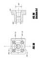
- FIG. 6Ais a front view of the upstream member showing the inner gas inlets and the outer gas inlets.
- FIG. 6Bis a side view of the upstream member.
- FIG. 6Cis another side view of the upstream member.
- FIG. 7Ais a rear view of the housing from FIG. 5B with the insert removed.
- FIG. 7Bis a cross-sectional view taken along lines C-C of FIG. 7A .
- FIG. 8Ais a front view of the insert from FIG. 5B .
- FIG. 8Bis a cross-sectional view taken along lines B-B of FIG. 8A and illustrates a circular flow path around a cone portion of the insert.
- FIG. 9Ais a rear view of a downstream member of the mixer assembly (shown attached to the upstream member in FIG. 3 ).
- FIG. 9Bis a cross-sectional view taken along line X-X of FIG. 9A , illustrating a reduction in the open cross-section area as the mixture flows through the downstream member.
- FIG. 10Ais bottom view of a transfer tube and the intake plenum from FIG. 3 illustrating the gas entering the transfer tube and exiting from the intake plenum.
- FIG. 10Bis a front view of the transfer tube and the intake plenum from FIG. 10A .
- FIG. 10Cis a top view of the transfer tube and the intake plenum from FIG. 10A .
- FIG. 11is a flow diagram illustrating a process for atomic layer deposition.
- FIG. 1Ais a perspective view of an ALD device 100 .
- the ALD device 100comprises a top member 110 , a bottom member 112 , and a front member 118 which together form a portion of a housing for the ALD device 100 .
- an upper heater 114extends through the top member 110 .
- the upper heater 114is configured to maintain the temperature in the upper portion of the ALD device 100 .
- a lower heater 116extends through the bottom member 112 .
- the lower heateris configured to maintain the temperature in the lower portion of the ALD device 100 .
- the front member 118which serves as a gate valve, of the ALD device 100 covers an opening 120 .
- a dashed lineoutlines the opening 120 in FIG. 1A .
- An ALD control system(not shown) is configured to control the ALD device 100 during processing of the wafer.
- the ALD control systemcan include a computer control system and electrically controlled valves to control the flow of reactant and buffer gases into and out of the ALD device 100 .
- the ALD control systemcan include modules such as a software or hardware component, such as a FPGA or ASIC, which performs certain tasks.
- a modulemay advantageously be configured to reside on the addressable storage medium of the computer control system and be configured to execute on one or more processors.
- FIG. 1Bis a perspective view of the ALD device 100 showing the bottom member 112 .
- the ALD device 100further comprises couplings 102 ( a ), 102 ( b ) and couplings 104 ( a )-( d ).
- ALD device 100includes four separate reactant vapor sources. Two of these reactant vapor sources are connected to the ALD device 100 via couplings 102 ( a ), 102 ( b ). These gas sources can be pressurized or not. These vapor sources can be, for example, solid sublimation vessels, liquid bubblers or gas bombs. The third and fourth reactant vapor sources are connected to the ALD device 100 via couplings 104 ( b ), 104 ( c ).
- Each reactant vapor sourcehas an associated inert gas source which is used to purge the reactant vapor lines after pulsing the reactant.
- the inert gas sources that are associated with the reactant vapor sources connected to couplings 102 ( a ) and 102 ( b )are connected to couplings 104 ( a ) and 104 ( d ), respectively.
- the inert gas sources associated with the reactant vapor sources connected to couplings 104 ( b ) and 104 ( c )are also connected to couplings 104 ( b ) and 104 ( c ), respectively.
- These inert gas sourcescan be pressurized or not.
- These inert gas sourcescan, be, for example, noble or nitrogen gas sources.
- the ALD control system(not shown) controls one or more valves to selectively allow or prevent the various gases from reaching the ALD device 100 .
- the ALD device 100is configured to deposit a thin film on the wafer when the wafer is inserted in the deposition chamber.
- the ALD device 100receives a first reactant gas via one of the couplings 102 ( a ), 102 ( b ) or one of the couplings 104 ( b ), 104 ( c ).
- the ALD device 100also receives inert gas via the couplings 104 ( a )- 104 ( d ).
- the inert gasenters the deposition chamber with the first reactant gas to adsorb no more than a monolayer of the first reactant on the wafer.
- the flow of the first reactant gasis stopped via an inert gas valving (IGV) arrangement and the deposition chamber and the gas lines are then purged with the inert gas from couplings 104 ( a ), 104 ( b ), 104 ( c ), and 104 ( d ).
- IGVinert gas valving
- the deposition cycleis continued with one or more of the other reactant gases.
- the reactants from alternated pulsesreact with each other on the substrate or wafer surface to form no more than a single monolayer of the desired product in each cycle. It should be noted that variation of true ALD operation can increase deposition speed above one monolayer per cycle with some sacrifice to uniformity.
- more than two reactant gasesare sequentially flowed (separated by periods of purging) through the ALD device 100 in each cycle to form compound materials on the wafer. Excess of each reactant gas is subsequently exhausted via gas exit 106 ( FIG. 1B ) after adsorbing or reacting in the deposition chamber.
- the gas exit 106may be connected to a vacuum pump to assist in the removal of the gases from the deposition chamber and provide a low pressure condition in the deposition chamber.
- the entire ALD device 100can be pumped down to a low pressure by connecting any of the other couplings on the bottom member 112 to a vacuum pump.
- FIG. 2is a cut-away section view of the ALD device 100 from FIG. 1A taken along line 2 - 2 .
- a gas distribution system 202Within the ALD device 100 is a gas distribution system 202 and a deposition chamber 200 .
- a dashed linecircumscribes the gas distribution system 202 .
- the ALD device 100further includes a wafer support 204 , a wafer support heater 216 , and a thermal switch 218 .
- the wafer support 204is located within the ALD device and is configured to support a substrate or wafer during the deposition process.
- the wafer support 204can be adapted to rotate within the deposition chamber 200 .
- the wafer support heater 216is configured to heat the wafer support 204 .
- the thermal switch 218is provided on the top member 110 .
- the thermal switch 218is configured to monitor the temperature of the top member 110 . It will be understood that the system 100 includes other temperature sensor and control mechanisms to maintain various surfaces of the system at desired temperatures.
- the upper reflector plates 208provide a thermal barrier between the upper portion of the gas distribution system 202 and the top member 110 .
- lower reflector plates 210provide a thermal barrier between the lower portion of the deposition chamber 200 and the bottom member 112 .
- the reflector plates 208 and 210are also used to assist in radiatively heating the deposition chamber within a low pressure environment.
- the upper heater 114is coupled to coils 212 which extend through the upper reflector plates 208 .
- the coils 212are configured to provide heat through radiation to the upper portion of the gas distribution system 202 .
- the lower heater 116is coupled to coils 214 which extend through the lower reflector plates 210 and heat the lower portion of the deposition chamber 200 .
- other heating systemscan be employed.
- the gas distribution system 202is configured to route reactant gases entering via the couplings 102 ( a ), 102 ( b ), 104 ( b ), 104 ( c ) and inert gases entering via couplings 104 ( a )-( d ) through the ALD device 100 (see FIG. 1B ).
- the gas distribution system 202is further configured to selectively mix one or more of the inert gases entering via couplings 104 ( a )-( d ) with one of reactant gases entering via couplings 102 ( a ), 102 ( b ), 104 ( b ), 104 ( c ) during a given pulse.
- the resulting mixtureenters the deposition chamber 200 .
- the gas distribution system 202exhausts any unreacted reactant and inert gases from the deposition chamber via gas exit 106 , such as through purging.
- the term couplingis used to describe a gas flow connection between one or more gas lines.
- the locations of the couplings shown hereinare for illustrative purposes only and can be located at different locations along a gas line.
- a gas line associated with a given couplingcan be configured to flow gas into or out of the gas distribution system 202 .
- the various couplings in the exemplary embodiments described hereinare designated to flow gases into or out of the gas distribution system 202 .
- the inventionis not limited to the exemplary embodiments disclosed herein.
- the order that the reactant gases are cycled through the ALD device 100depends on the desired product.
- the inert gas entering via couplings 104 ( a )-( d )is periodically cycled or continuously flowed through the ALD device 100 between pulses of the reactant gases. In this way, the inert gases purge the deposition chamber 200 .
- various reactant gases and inert gasesare systematically cycled through the ALD device 100 so as to form a deposit on the wafer inserted through the opening 120 .
- FIG. 3is a perspective view of the deposition chamber 200 and the gas distribution system 202 from the ALD device 100 of FIG. 1A .
- the gas distribution system 202comprises a plurality of gas lines, a mixer assembly 304 , a transfer tube 310 , and an intake plenum or manifold 312 .
- the deposition chamber 200includes a cover plate 314 , a base plate 206 , and an exhaust launder 316 .
- the gas distribution system 202is connected to the deposition chamber 200 at the intake plenum 312 .
- the plurality of gas linesinclude four reactant lines 300 , 303 , 309 , 315 and eight buffer lines 301 , 302 , 305 , 307 , 311 , 313 , 317 , and 319 .
- Each reactant lineis coupled with two of the buffer lines.
- Reactant line 300is coupled to buffer lines 301 , 302 .
- Reactant line 303is coupled to buffer lines 305 , 307 .
- Reactant line 307is coupled to buffer lines 311 , 313 .
- Reactant line 315is coupled to buffer lines 317 , 319 .
- the gas distribution system 202can include greater or fewer reactant lines and buffer lines depending on the configuration of the ALD device 100 .
- each reactant linemay or may not be coupled to two buffer lines.
- one or more of the reactant linesmay be coupled to the buffer lines while another reactant line is not.
- the reactant line that is not coupled to buffer linescould be shut off by other means.
- Each reactant gas lineincludes four couplings within the gas distribution system 202 .
- Reactant gas line 300comprises couplings 300 ( a ), 300 ( b ), 300 ( c ), and 300 ( d ).
- Reactant gas line 303comprises couplings 303 ( a ), 303 ( b ), 303 ( c ), and 303 ( d ).
- Reactant gas line 309comprises couplings 309 ( a ), 309 ( b ), 309 ( c ), and 309 ( d ).
- Reactant gas line 315comprises couplings 315 ( a ), 315 ( b ), 315 ( c ), and 315 ( d ). The couplings for each reactant gas line are described below.
- Coupling 300 ( a )couples the reactant gas line 300 with the coupling 102 ( b ) that leads to a reactant source (see FIG. 1B ).
- Coupling 300 ( b )couples the reactant gas line 300 with the buffer line 302 .
- Coupling 300 ( c )couples the reactant gas line 300 with the buffer line 301 .
- Coupling 300 ( d )couples the reactant gas line 300 with the mixer assembly 304 .
- Coupling 303 ( a )couples the reactant gas line 303 with the coupling 104 ( b ) that leads to another reactant source (see FIG. 1B ).
- Coupling 303 ( b )couples the reactant gas line 303 with the buffer line 307 .
- Coupling 303 ( c )couples the reactant gas line 303 with the buffer line 305 .
- Coupling 303 ( d )couples the reactant gas line 303 with the mixer assembly 304 .
- Coupling 309 ( a )couples the reactant gas line 309 with the coupling 104 ( c ) that leads to another reactant source. (see FIG. 1B ).
- Coupling 309 ( b )couples the reactant gas line 309 with the buffer line 313 .
- Coupling 309 ( c )couples the reactant gas line 309 with the buffer line 311 .
- Coupling 309 ( d )couples the reactant gas line 309 with the mixer assembly 304 .
- Coupling 315 ( a )couples the reactant gas line 315 with the coupling source 102 ( a ) that leads to still another reactant source (see FIG. 1B ).
- Coupling 315 ( b )couples the reactant gas line 315 with the buffer line 319 .
- Coupling 315 ( c )couples the reactant gas line 315 with the buffer line 317 .
- Coupling 315 ( d )couples the reactant gas line 315 with the mixer assembly 304 .
- Buffer lines 301 , 302 , 305 , 307 , 311 , 313 , 317 , and 319comprise couplings 301 ( a ), 302 ( a ), 305 ( a ), 307 ( a ), 311 ( a ), 313 ( a ), 317 ( a ), and 319 ( a ), respectively.
- each coupling 301 ( a ), 305 ( a ), 311 ( a ), and 317 ( a )provides a flow path into the gas distribution system 202 .
- the coupling 301 ( a )couples the buffer line 301 with the coupling 104 ( a ) (see FIG. 1B ).
- the coupling 305 ( a )couples the buffer line 305 with the coupling 104 ( b ) (see FIG. 1B ).
- the coupling 311 ( a )couples the buffer line 311 with the coupling 104 ( c ) (see FIG. 1B ).
- the coupling 317 ( a )couples the buffer line 317 with the coupling 104 ( d ) (see FIG. 1B ).
- Each coupling 302 ( a ), 307 ( a ), 313 ( a ), and 319 ( a )provides a flow path between the gas distribution system 202 and the exhaust launder 316 via connectors 320 ( a )-( d ).
- Connector 320 ( a )connects coupling 302 ( a ) with the exhaust launder 316 .
- Connector 320 ( b )connects coupling 307 ( a ) with the exhaust launder 316 .
- Connector 320 ( c )connects coupling 313 ( a ) with the exhaust launder 316 .
- Connector 320 ( d )connects coupling 319 ( a ) with the exhaust launder 316 .
- the reactant gas lines 300 , 303 , 309 , and 315route reactant gases to the mixer assembly 304 .
- the buffer lines 301 , 305 , 311 , and 317route inert gases to the mixer assembly 304 .
- the resulting mixture(one reactant at a time with an inert gas) flows through a transfer tube 310 to an intake plenum 312 .
- the intake plenum 312distributes the mixture in a transverse direction with respect to the flow path through the transfer tube 310 .
- the mixtureexits the intake plenum 312 into the deposition chamber 200 through the cover plate 314 . As shown in FIGS.
- the cover plate 314lies adjacent to the base plate 206 and the two plates form a flow path there between for the mixture to flow over the substrate or wafer placed on the wafer support 204 .
- the base plate 206 and the cover plate 314have substantially rectangular outer perimeters.
- the mixtureWhile traversing the deposition chamber 200 , the mixture pulse saturates the surface of the substrate. Adsorption or reaction occurs between the current mixture and the surface of the substrate as left by the previous pulse may occur.
- the mixtureflows towards the exhaust launder 316 .
- the exhaust launder 316is configured to collect excess of the mixture and any byproduct after the mixture has saturated the wafer.
- a region within the exhaust launder 316is at a lower pressure than the pressure in the deposition chamber 200 .
- a negative pressure source or vacuumcan be in flow communication with the exhaust launder 316 and/or gas exit 106 to draw the mixture from the deposition chamber 200 .
- the exhaust launder 316is in flow communication with the gas exit 106 .
- the collected mixtureexits the deposition chamber 200 via the gas exit 106 .
- the mixer assembly 304includes an upstream member 306 and a downstream member 308 .
- the upstream member 306is in flow communication with the reactant gas lines and the buffer lines.
- the upstream member 306is configured to mix the reactant gas with the inert gas prior to the mixture entering the downstream member 308 .
- the downstream member 308funnels the mixture between the upstream member 306 and the transfer tube 310 .
- the downstream member 308is configured to minimize the tendency of the mixture to re-circulate within the downstream member 308 by continually reducing cross-sectional area of the flow path for the mixture.
- FIG. 4is a top plan view of the reactant gas lines coupled to the buffer lines and the upstream member 306 of the mixer assembly.
- a buffer region 400 ( a )is formed in the reactant gas line 300 .
- a buffer region 400 ( b )is formed in the reactant gas line 303 .
- a buffer region 400 ( c )is formed in the reactant gas line 309 .
- a buffer region 400 ( d )is formed in the reactant gas line 315 .
- the buffer lines 301 , 305 , 311 , and 317which form flow paths into the gas distribution system 202 , couple to their associated gas lines downstream of couplings 300 ( b ) 303 ( b ), 309 ( b ), and 315 ( b ).
- gas entering via couplings 301 ( a ), 305 ( a ), 311 ( a ), and 317 ( a )enters the reactant lines 300 , 303 , 309 , 315 downstream of the reactant lines couplings with the buffer lines 302 , 307 , 311 , and 319 .
- Fixed orificescan be placed at couplings 302 ( a ), 307 ( a ), 313 ( a ) and 319 ( a ).
- couplings 302 ( a ), 307 ( a ), 313 ( a ) and 319 ( a )are in communication with the exhaust launder 316 .
- the orificescreate a higher resistance path for the gases to flow to the exhaust launder 316 and bypass the deposition chamber 200 .
- a small portion of the reactant gas entering via couplings 300 ( a ), 303 ( a ), 309 ( a ) or 315 ( a )bypasses the deposition chamber and flows directly to the exhaust launder 316 .
- the restriction created by the orificelimits the amount of shunted reactant.
- the inert gas entering via couplings 301 ( a ), 305 ( a ), 311 ( a ), and 317 ( a )creates a reverse flow towards couplings 300 ( b ) 303 ( b ), 309 ( b ), and 315 ( b ) to form the buffer regions 400 ( a )-( d ) within the reactant gas line.
- the buffer regionskeep the reactant gases from diffusing into the reactor during the purge steps or during reactant flow of a reactant from one of the other reactant lines into the mixer assembly 304 .
- reactant gasflows through reactant line 300 towards the upstream member 306 of the mixer assembly.
- a small amount of this reactant gasis diverted to the buffer line 302 and out through coupling 302 ( a ) into the exhaust launder 316 .
- the amount of gas that is diverted to the buffer lineis dependent of the size of the fixed orifice at coupling 302 ( a ).
- the size of the fixed orificecan be changed to divert more or less of the gas into the exhaust launder 316 .
- the remaining reactant gasflows through the buffer region 400 ( a ) to the coupling 300 ( c ).
- Inert gasmay or may not be introduced through coupling 301 ( a ) to push the reactant gas into the upstream member 306 . If inert gas is introduced through coupling 301 ( a ), the inert gas joins the reactant gas at coupling 300 ( c ) and flows to the upstream member 306 . After the pulse step, the reactant gas is purged from the gas line. Purging of the gas line can be accomplished by, for example, shutting off the flow of the reactant gas from coupling 300 ( a ) and/or using the inert gas to impede the diffusion of any remaining reactant gas into the upstream member 306 . The shutoff valve can be located outside of the heated area and can be used to shut off the flow of the reactant gas.
- the inert gascan be introduced through coupling 301 ( a ) in an inert gas valving (IGV) process as described generally in U.S. patent publication No. 2001/0054377, published on Dec. 27, 2001, the disclosure of which is hereby incorporated herein by reference.
- IGVinert gas valving
- a first portion of the stream of inert gas flowenters the buffer region 400 ( a ) and flows upstream or backwards towards the coupling 300 ( b ).
- a second portion of the stream of gasflows downstream towards the upstream member 306 .
- the first portionexits the reactant line 300 at the end of the buffer region 400 ( a ) and enters the buffer line 302 . While the first portion is flowing through the buffer region 400 ( a ), the remaining reactant gas between the shutoff valve upstream of coupling 300 ( a ) and coupling 300 ( b ) is blocked from flowing or diffusing to the upstream member 306 without subjecting physical valves (which are remote) to the wear caused by high temperatures.
- the first portionforms a buffer or diffusion barrier (or inert gas valve) that impedes the flow of the reactant gas through the reactant line 300 to the mixer assembly 304 .
- the ALD control systemBy cycling the shutoff valve upstream of coupling 300 ( a ), the ALD control system is able to control between flowing and not flowing the inert gas in the buffer line 301 . In this way, the ALD control system is able to quickly control whether the reactant gas entering the reactant line 300 via coupling 300 ( a ) reaches the upstream member 306 .
- the reactant gas in a “dead space” which is located between the shutoff valve upstream of the coupling 300 ( a ) and coupling 300 ( b )can be kept from diffusing into the upstream member 306 . This may be advantageous for ALD since the different reactant gases are kept separated and only react on the surface of the substrate and not in the gas phase.
- Whether the reactant gas entering the gas distribution system 202 via the coupling 303 ( a ) reaches the upstream member 306is similarly controlled by flowing a gas through the buffer line 305 and into the reactant line 303 at coupling 303 ( c ) and using a shutoff valve upstream of coupling 303 ( a ).
- a first portion of the gas entering the reactant line at coupling 303 ( c )forms the buffer 400 ( b ). In this way, the first portion of the gas impedes the reactant gas entering via the reactant line 303 from entering the upstream member 306 .
- a second portion of the gas entering the reactant line at coupling 303 ( c )flows away from the buffer region 400 ( b ) and towards the upstream member 306 .
- Whether the reactant gas entering the gas distribution system 202 via the coupling 309 ( a ) reaches the upstream member 306is similarly controlled by flowing a gas through the buffer line 311 and into the reactant line 309 at coupling 309 ( c ) and using a shutoff valve upstream of coupling 309 ( a ).
- a first portion of the gas entering the reactant line at coupling 309 ( c )forms the buffer 400 ( c ). In this way, the first portion of the gas impedes the reactant gas entering via the reactant line 309 from entering the upstream member 306 .
- a second portion of the gas entering the reactant line at coupling 309 ( c )flows away from the buffer region 400 ( c ) and towards the upstream member 306 .
- Whether the reactant gas entering the gas distribution system 202 via the coupling 315 ( a ) reaches the upstream member 306is similarly controlled by flowing a gas through the buffer line 317 and into the reactant line 315 at coupling 315 ( c ) and a shutoff valve upstream of coupling 315 ( a ).
- a first portion of the gas entering the reactant line at coupling 315 ( c )forms the buffer 400 ( d ). In this way, the first portion of the gas impedes the reactant gas entering via the reactant line 315 from entering the upstream member 306 .
- a second portion of the gas entering the reactant line at coupling 315 ( c )flows away from the buffer region 400 ( d ) and towards the upstream member 306 .
- the first portions of the inert gasesbypass the deposition chamber 200 and are collected by the exhaust launder 316 downstream of the deposition chamber 200 .
- the second portions of each gas which enter the gas distribution system 202 via buffer lines 301 , 305 , 311 , and 317flow away from the buffer regions 400 ( a )-( d ) and enter the mixer assembly 304 .
- the second portionsmix with one or more reactant gases from other reactant lines, which reach the mixer assembly 304 .
- the second portionsflow through the deposition chamber 200 .
- gasesmay periodically flow through their respective buffer lines 301 , 305 , 311 , and 317 .
- a reactant gas which the ALD control system desires to reach the deposition chamber 200flows through its respective reactant line and into the mixer assembly 304 .
- the ALD control systemforms buffer regions 400 in the reactant lines associated with the reactant gases which the ALD control system does not want to reach the deposition chamber 200 .
- the reactant gas which flows through the reactant line which does not have a buffer region 400mixes with the second portions of the one or more inert gases which are simultaneously flowing through the other reactant lines and into the mixer assembly 304 . As explained above, the first portions of these gases form buffer regions in the other reactant lines and bypass the deposition chamber 200 .
- each reactant gasalternates in reaching the mixer assembly 304 .
- the reactant gas selected by ALD control systemflows into the mixer assembly 304 while inert or “buffer” gas flows in the remaining three reactant lines.
- the second portions of the gases flowing away from the buffer regionsenter the mixer assembly 304 .
- the reactant gas of the pulse of interestthen mixes with the inert gas of the second portions in the mixer assembly 304 .
- the mixer assembly 304will be described in detail with reference to FIGS. 5-8 .
- FIG. 5Ais a rear view of the upstream member 306 from FIG. 4 that illustrates a circular flow path 504 through the upstream member 306 .
- FIG. 5Bis a cross-sectional view taken along line A-A of FIG. 5A .
- the upstream member 306includes a housing 500 and an insert section 502 .
- the housing 500can have a square exterior shape with a non-tapered, cylindrical section (illustrated as 518 ) and tapered, conical section (illustrated as 520 ) extending therethrough.
- a narrowing conical inner surface 503 on the inside diameter of the housing 500narrows in a downstream direction towards the deposition chamber 200 .
- the inner surface 503 of the upstream member 306forms an upstream member housing mixing surface 516 .
- the upstream member 306can be made of one piece or separate pieces.
- the housing 500further includes at least a first inlet 600 ( a ), 600 ( b ), 602 ( a ), 602 ( b ).
- the housingincludes inner gas inlets 600 ( a ) and 600 ( b ) and outer gas inlets 602 ( a ) and 602 ( b ).
- the inner gas inlets 600 ( a ) and 600 ( b ) and the outer gas inlets 602 ( a ) and 602 ( b )are in flow communication with the reactant lines 300 , 303 , 309 , and 315 (see FIG. 4 ).
- the inner gas inlet 600 ( a )connects with the reactant line 300 at coupling 300 ( d ).
- the inner gas inlet 600 ( b )connects with the reactant line 315 at coupling 315 ( d ).
- the outer gas inlet 602 ( a )connects with the reactant line 303 at coupling 303 ( d ).
- the outer gas inlet 602 ( b )connects with the reactant line 309 at coupling 309 ( d ).
- the inner gas inlets 600 ( a ) and 600 ( b ) and the outer gas inlets 602 ( a ) and 602 ( b )can have elements of symmetry with respect to the centerline 508 .
- the inner gas inlets 600 ( a ) and 600 ( b )are located between the centerline 508 and the outer gas inlets 602 ( a ) and 602 ( b ).
- the outer gas inlets 602 ( a ) and 602 ( b )can be located to provide tangential in-flow into the upstream member 306 .
- the insert section 502can comprise a cone portion 506 or other three dimensional geometric shape.
- a pyramid shape, parabolic shape, hemispherical shape, or combination of one or more shapescould be used.
- a combination of a hemispherical base with a pyramid shape topcould be used for the insert portion 502 .
- the illustrated cone portion 506includes a base 510 and a distal end 512 .
- the conical surface or cone portion 506extends from the base 510 of the insert in a downstream direction towards the distal end 512 .
- a circumference of the cone portion 506 at the distal end 512is less than a circumference of the base 510 . In this way, the geometric shape of the insert section 502 narrows or tapers in a downstream direction towards the deposition chamber 200 .
- a surface of the cone portion 506forms an insert mixing surface 514 .
- the insert mixing surface 514extends between the base 510 and the distal end 512 . In the embodiment depicted in FIG. 5B , nearly all of the insert mixing surface 514 is parallel to the upstream member housing mixing surface 516 .
- the insert mixing surface 514 and the upstream member housing mixing surface 516may not be parallel.
- the insert mixing surface 514could have a pyramid shape while the upstream member housing mixing surface 516 could have a conical shape but preferably both surfaces are smooth.
- the outer surface of the insert and the inner surface of the housingpreferably define a passage therebetween and the passage preferably is annular about the mixer flow axis 505 .
- the passagepreferably is defined by tapering surfaces to form a funnel. Either of the mixing surfaces 514 , 516 can be a first mixing surface with the remaining surface being the second mixing surface.
- Surface 507 of the insert 502can be formed to match the radius of the intersecting inner gas inlets 600 ( a ) and 600 ( b ) and the outer gas inlets 602 ( a ) and 602 ( b ).
- the surface 507can be in the shape of a trough which circumscribes the base 510 .
- a cross-section of the troughmatches the radius of the outer gas inlets 602 ( a ) and 602 ( b ).
- the surface 507forms a transition surface between the insert mixing surface 514 and the upstream member housing mixing surface 516 . In this way, turbulence and recirculation can be reduced in the upstream member 306 .
- the annular passagethus serves as a mixing chamber between the downstream member 308 (see FIG. 3 ), the insert mixing outer surface 514 , housing mixing inner surface 516 , and the surface 507 .
- the cone portion 506reduces gas recirculation in the center of the upstream member 306 . Since the housing mixing surface 516 narrows in a downstream direction towards the deposition chamber 200 , the distance between the outside surface of the cone portion 506 and the inner conical surface of the housing 500 can be parallel. The parallel surfaces allow a linear decrease in the cross-sectional area as traced by the flow path through the upstream member 306 .
- a racetrack region or annular passage 504is formed between the outside surface of the cone portion 506 and the inner conical surface of the housing 500 . Due to the offset locations of the inner gas inlet 600 ( a ) and 600 ( b ) and the outer gas inlets 602 ( a ) and 602 ( b ) with respect to the centerline 508 , the reactant gas and any second portions of the gases from the buffer lines enter the annular passage 504 at different locations. For example, the outer gas inlets 602 ( a ) and 602 ( b ) are substantially aligned with a cross-section of the trough which circumscribes the base 510 .
- the gasesfollow the annular passage and swirl around the cone portion 506 as the gases move through the upstream member 306 and towards the deposition chamber 200 .
- the annular passage 504enhances the mixing of the reactant gas with the second portions of the inert gases within the upstream member 306 .
- the upstream member 306mixes the gases in three dimensions.
- the cross-sectional area between the housing 500 and the insert 502decreases as the mixture moves towards the downstream member 308 (see FIG. 3 )
- the velocity of the mixtureincreases. This increase in mixture velocity aids in the mixing process.
- FIG. 6Ais a front view of the upstream member 306 showing the inner gas inlets 600 ( a ) and 600 ( b ) and the outer gas inlets 602 ( a ) and 602 ( b ).
- FIGS. 6B and 6Care side views of the upstream member 306 .
- the inner gas inlets 600 ( a ) and 600 ( b ) and the outer gas inlets 602 ( a ) and 602 ( b )are in flow communication with the reactant gas lines shown in FIG. 4 .
- the inside surfaces of the insert 502 and the housing 500are shown in phantom lines.
- FIG. 7Ais a rear view of the housing 500 from FIG. 5A with the insert 502 removed.
- FIG. 7Bis a cross-sectional view taken along line C-C of FIG. 7A .
- the housing 500can have a square exterior shape with a partially cylindrical and partially conical cavity extending therethrough. A narrowing conical surface on the inside diameter of the housing 500 extends in a downstream direction towards the deposition chamber 200 .
- the housing 500further includes attachment holes 700 ( a )-( d ) on the downstream or rear surface for attaching the upstream member 306 to the downstream member 308 (see FIG. 3 ).
- FIG. 8Ais a front view of the insert 502 from FIG. 5A .
- FIG. 8Bis a cross-sectional view taken along line B-B of FIG. 8A and illustrates a spiral flow path 800 around a cone portion 506 of the insert. As illustrated, the gas mixture circles around the cone 506 (through the frustoconical passage) as the mixture migrates towards the deposition chamber 200 .
- FIG. 9Ais a rear view of the downstream member 308 of the mixer assembly 304 from FIG. 3 .
- FIG. 9Bis a cross-sectional view taken along line X-X of FIG. 9A illustrating a reduction in the open cross-section area as the mixture flows through the downstream member.
- the upstream member 306is not shown.
- the downstream member 308has a general funnel shape along an inside surface.
- the downstream member 308includes a downstream member entrance 900 and a downstream member exit 902 .
- the cross-sectional area of the downstream member entrance 900is greater than the cross-sectional area of the downstream member exit 902 .
- the cross-sectional flow area of the downstream member 308gradually decreases as the mixture migrates towards the downstream member exit 902 to form a tapered or “funnel” passage therebetween.
- the downstream member 308further includes attachment holes 904 ( a )-( d ).
- the attachment holes 904 ( a )-( d )align with the attachment holes 700 ( a )-( d ) (see FIG. 7A ) for attaching the upstream member 306 to the downstream member 308 . Controlling the machining tolerances on the attachment holes 904 ( a )-( d ) can aid in aligning the upstream member 306 with the downstream member 308 thereby reducing recirculation within the mixer assembly 304 .
- Controlling the surface finish and flatness on the mating surfaces of the upstream member 306 (see FIGS. 5A and 5B ) and the downstream member 308can aid in sealing the upstream member with the downstream member.
- a 16 micro finish surfaceis maintained.
- FIG. 10Ais bottom view of the transfer tube 310 and the intake plenum 312 from FIG. 3 illustrating the gas entering the transfer tube and exiting from the intake plenum.
- FIG. 10Bis a front view of the transfer tube 310 and the intake plenum 312 from FIG. 3 .
- FIG. 10Cis a top view of the transfer tube 310 and the intake plenum 312 from FIG. 3 .
- the transfer tube 310connects with the downstream member 308 (see FIG. 9A ).
- the mixtureflows from the mixer assembly 304 into the transfer tube 310 via an intake plenum entrance 1000 before entering the intake plenum 312 .
- the mixtureis then distributed in the intake plenum 312 prior to the mixture exiting the intake plenum 312 via intake plenum exits 1002 .
- the mixturepasses through the cover plate 314 whereby it enters the deposition chamber 200 .
- FIG. 11is a flow diagram illustrating a process for atomic layer deposition.
- the order of the states in FIG. 11is exemplary only. In this exemplary process, only the reactant gas entering via reactant line 315 is selected for entering the deposition chamber 200 .
- the processbegins at a state 1100 where one or more reactant gases flow into the gas distribution system 202 via couplings 300 ( a ), 303 ( a ), 309 ( a ), and 315 ( a ) (see FIGS. 3 and 4 ).
- the reactant gasflows through its respective reactant line gas line 300 ( a ), 303 ( a ), 309 ( a ), and 315 ( a ) and towards the mixer assembly 304 .
- Flowproceeds to a state 1102 where one or more inert gases flow into buffer lines 301 , 305 , and 311 via couplings 301 ( a ), 305 ( a ), and 311 ( a ).
- the processmoves to a state 1104 where buffer regions 400 ( a )-( c ) are formed between couplings 300 ( c ) and 300 ( b ), 303 ( c ) and 303 ( b ), and 309 ( c ) and 309 ( b ).
- the only reactant gas that reaches the mixer assembly 304is the reactant gas entering via coupling 315 ( a ) and flows through reactant line 315 .
- buffer regions 400 ( a )-( c )prevent the reactant gases entering via couplings 300 ( a ), 303 ( a ), and 309 ( a ) from reaching the mixer assembly 304 .
- the buffer regionsare formed before the reactant gas flows towards the mixer assembly 304 .
- one or more buffer regionscan be formed before one or more of the reactant gases flows towards the mixer assembly 304 .
- the processmoves to a state 1106 where the reactant gas from the reactant line 315 is mixed with second portions of each of the inert gases entering via buffer lines 301 , 305 , and 311 .
- the reactant gas and the second portions of the inert gasesform a gas mixture in the mixer assembly 304 .
- Each of the gasesenters the mixer assembly at different locations around the circumference of the mixer assembly 304 .
- the entering gasesswirl around the cone portion 506 (see FIG. 5A ) as the gas passes through the mixer assembly 304 . Further, the cross-sectional area in the mixer assembly decreases as the mixture flows through the mixer assembly 304 and towards the transfer tube 310 .
- the processcontinues to a state 1108 where the gas mixture flows into a deposition chamber 200 to adsorb or otherwise react on a substrate.
- the processmoves to a state 1110 where excess mixture and any by-product are exhausted into an exhaust launder 316 .
- the processproceeds to a state 1112 where a first portion of each of the inert gases from the inert buffer regions 400 ( a )-( c ) exhausts into the exhaust launder 316 via buffer lines 302 , 307 , and 313 .
- Flowcontinues to a state 1114 where the deposition chamber 200 is purged.
- the next desired reactant gasenters the gas distribution system 202 via coupling 309 ( a ). Since only the reactant gas entering via coupling 309 ( a ) is desired, in the present example, inert gas buffer regions 400 ( a ), 400 ( c ), and 400 ( d ) are formed by flowing gas through the buffer lines 301 , 305 , and 311 .
- the reactant gas entering via coupling 309 ( a )flows through reactant line 309 and mixes with second portions of each of the inert gases.
- the second portions of the inert gasesenter the reactant lines at couplings 300 ( c ), 303 ( c ), and 315 ( c ) and flow towards the mixer assembly 304 .
- the second portionsform a second gas mixture with the reactant gas entering via reactant line 309 .
- the processmoves to a state 1120 where the second gas mixture flows into the deposition chamber 200 to react with the deposit on the wafer.
- a state 1122the excess second mixture and any by-product is exhausted into the exhaust launder 316 .
- the processmoves to a state 1124 where a first portion of each of the inert gases from the inert gas buffer regions 400 ( a ), 400 ( c ), and 400 ( d ) are exhausted into the exhaust launder 316 .
- the first portionis exhausted to the exhaust launder 316 without passing through the mixer assembly 304 .
- one or more of the disclosed featureslend themselves to improve mixing during ALD processing.
- the construction of the mixerlends itself to ready disassembly, cleaning and replacement of any “pre-reaction product.”
- the use of a pre-reaction chamber arranged upstream of the deposition or reactor chamber to reduce the residue of a preceding reactant during ALD processingis disclosed in U.S. patent publication No. 2002/0108570, published on Aug. 15, 2002, the disclosure of which is incorporated herein by reference.
Landscapes
- Chemical & Material Sciences (AREA)
- General Chemical & Material Sciences (AREA)
- Chemical Kinetics & Catalysis (AREA)
- Engineering & Computer Science (AREA)
- Materials Engineering (AREA)
- Mechanical Engineering (AREA)
- Metallurgy (AREA)
- Organic Chemistry (AREA)
- Chemical Vapour Deposition (AREA)
Abstract
Description
Claims (26)
Priority Applications (3)
| Application Number | Priority Date | Filing Date | Title |
|---|---|---|---|
| US10/929,348US8152922B2 (en) | 2003-08-29 | 2004-08-30 | Gas mixer and manifold assembly for ALD reactor |
| US12/398,938US8465801B2 (en) | 2003-08-29 | 2009-03-05 | Gas mixer and manifold assembly for ALD reactor |
| US13/316,372US8784563B2 (en) | 2003-08-29 | 2011-12-09 | Gas mixer and manifold assembly for ALD reactor |
Applications Claiming Priority (2)
| Application Number | Priority Date | Filing Date | Title |
|---|---|---|---|
| US49904503P | 2003-08-29 | 2003-08-29 | |
| US10/929,348US8152922B2 (en) | 2003-08-29 | 2004-08-30 | Gas mixer and manifold assembly for ALD reactor |
Related Child Applications (2)
| Application Number | Title | Priority Date | Filing Date |
|---|---|---|---|
| US12/398,938DivisionUS8465801B2 (en) | 2003-08-29 | 2009-03-05 | Gas mixer and manifold assembly for ALD reactor |
| US13/316,372ContinuationUS8784563B2 (en) | 2003-08-29 | 2011-12-09 | Gas mixer and manifold assembly for ALD reactor |
Publications (2)
| Publication Number | Publication Date |
|---|---|
| US20050092247A1 US20050092247A1 (en) | 2005-05-05 |
| US8152922B2true US8152922B2 (en) | 2012-04-10 |
Family
ID=34555643
Family Applications (3)
| Application Number | Title | Priority Date | Filing Date |
|---|---|---|---|
| US10/929,348Active2028-07-25US8152922B2 (en) | 2003-08-29 | 2004-08-30 | Gas mixer and manifold assembly for ALD reactor |
| US12/398,938Active2026-10-07US8465801B2 (en) | 2003-08-29 | 2009-03-05 | Gas mixer and manifold assembly for ALD reactor |
| US13/316,372Expired - LifetimeUS8784563B2 (en) | 2003-08-29 | 2011-12-09 | Gas mixer and manifold assembly for ALD reactor |
Family Applications After (2)
| Application Number | Title | Priority Date | Filing Date |
|---|---|---|---|
| US12/398,938Active2026-10-07US8465801B2 (en) | 2003-08-29 | 2009-03-05 | Gas mixer and manifold assembly for ALD reactor |
| US13/316,372Expired - LifetimeUS8784563B2 (en) | 2003-08-29 | 2011-12-09 | Gas mixer and manifold assembly for ALD reactor |
Country Status (1)
| Country | Link |
|---|---|
| US (3) | US8152922B2 (en) |
Cited By (291)
| Publication number | Priority date | Publication date | Assignee | Title |
|---|---|---|---|---|
| US20120079984A1 (en)* | 2003-08-29 | 2012-04-05 | Asm America, Inc. | Gas mixer and manifold assembly for ald reactor |
| US20120266821A1 (en)* | 2005-01-18 | 2012-10-25 | Asm America, Inc. | Reaction system for growing a thin film |
| US20130160709A1 (en)* | 2011-12-27 | 2013-06-27 | Asm America, Inc. | Vapor flow control apparatus for atomic layer deposition |
| US8871617B2 (en) | 2011-04-22 | 2014-10-28 | Asm Ip Holding B.V. | Deposition and reduction of mixed metal oxide thin films |
| US9379011B2 (en) | 2008-12-19 | 2016-06-28 | Asm International N.V. | Methods for depositing nickel films and for making nickel silicide and nickel germanide |
| US9574268B1 (en) | 2011-10-28 | 2017-02-21 | Asm America, Inc. | Pulsed valve manifold for atomic layer deposition |
| US9607842B1 (en) | 2015-10-02 | 2017-03-28 | Asm Ip Holding B.V. | Methods of forming metal silicides |
| WO2018109554A1 (en) | 2016-12-15 | 2018-06-21 | Asm Ip Holding B.V. | Method of forming a structure on a substrate |
| WO2018109552A1 (en) | 2016-12-15 | 2018-06-21 | Asm Ip Holding B.V. | Semiconductor processing apparatus |
| WO2019229537A2 (en) | 2018-06-01 | 2019-12-05 | Asm Ip Holding B.V. | Infiltration apparatus and methods of infiltrating an infiltrateable material |
| US20200133131A1 (en)* | 2018-10-30 | 2020-04-30 | Taiwan Semiconductor Manufacturing Co., Ltd. | Extreme Ultraviolet Photolithography Method with Infiltration for Enhanced Sensitivity and Etch Resistance |
| US10662527B2 (en) | 2016-06-01 | 2020-05-26 | Asm Ip Holding B.V. | Manifolds for uniform vapor deposition |
| US10872803B2 (en) | 2017-11-03 | 2020-12-22 | Asm Ip Holding B.V. | Apparatus and methods for isolating a reaction chamber from a loading chamber resulting in reduced contamination |
| US10872804B2 (en) | 2017-11-03 | 2020-12-22 | Asm Ip Holding B.V. | Apparatus and methods for isolating a reaction chamber from a loading chamber resulting in reduced contamination |
| US11004977B2 (en) | 2017-07-19 | 2021-05-11 | Asm Ip Holding B.V. | Method for depositing a group IV semiconductor and related semiconductor device structures |
| US11001925B2 (en) | 2016-12-19 | 2021-05-11 | Asm Ip Holding B.V. | Substrate processing apparatus |
| US11018002B2 (en) | 2017-07-19 | 2021-05-25 | Asm Ip Holding B.V. | Method for selectively depositing a Group IV semiconductor and related semiconductor device structures |
| US11015245B2 (en) | 2014-03-19 | 2021-05-25 | Asm Ip Holding B.V. | Gas-phase reactor and system having exhaust plenum and components thereof |
| US11022879B2 (en) | 2017-11-24 | 2021-06-01 | Asm Ip Holding B.V. | Method of forming an enhanced unexposed photoresist layer |
| US11031242B2 (en) | 2018-11-07 | 2021-06-08 | Asm Ip Holding B.V. | Methods for depositing a boron doped silicon germanium film |
| USD922229S1 (en) | 2019-06-05 | 2021-06-15 | Asm Ip Holding B.V. | Device for controlling a temperature of a gas supply unit |
| US11049751B2 (en) | 2018-09-14 | 2021-06-29 | Asm Ip Holding B.V. | Cassette supply system to store and handle cassettes and processing apparatus equipped therewith |
| US11056344B2 (en) | 2017-08-30 | 2021-07-06 | Asm Ip Holding B.V. | Layer forming method |
| US11053591B2 (en) | 2018-08-06 | 2021-07-06 | Asm Ip Holding B.V. | Multi-port gas injection system and reactor system including same |
| US20210207269A1 (en)* | 2020-01-06 | 2021-07-08 | Asm Ip Holding B.V. | Gas supply assembly, components thereof, and reactor system including same |
| US11069510B2 (en) | 2017-08-30 | 2021-07-20 | Asm Ip Holding B.V. | Substrate processing apparatus |
| US11081345B2 (en) | 2018-02-06 | 2021-08-03 | Asm Ip Holding B.V. | Method of post-deposition treatment for silicon oxide film |
| US11087997B2 (en) | 2018-10-31 | 2021-08-10 | Asm Ip Holding B.V. | Substrate processing apparatus for processing substrates |
| US11088002B2 (en) | 2018-03-29 | 2021-08-10 | Asm Ip Holding B.V. | Substrate rack and a substrate processing system and method |
| US11094582B2 (en) | 2016-07-08 | 2021-08-17 | Asm Ip Holding B.V. | Selective deposition method to form air gaps |
| US11094546B2 (en) | 2017-10-05 | 2021-08-17 | Asm Ip Holding B.V. | Method for selectively depositing a metallic film on a substrate |
| US11101370B2 (en) | 2016-05-02 | 2021-08-24 | Asm Ip Holding B.V. | Method of forming a germanium oxynitride film |
| US11107676B2 (en) | 2016-07-28 | 2021-08-31 | Asm Ip Holding B.V. | Method and apparatus for filling a gap |
| US20210272776A1 (en)* | 2018-01-25 | 2021-09-02 | Applied Materials, Inc. | Dogbone inlet cone profile for remote plasma oxidation chamber |
| US11114283B2 (en) | 2018-03-16 | 2021-09-07 | Asm Ip Holding B.V. | Reactor, system including the reactor, and methods of manufacturing and using same |
| US11114294B2 (en) | 2019-03-08 | 2021-09-07 | Asm Ip Holding B.V. | Structure including SiOC layer and method of forming same |
| USD930782S1 (en) | 2019-08-22 | 2021-09-14 | Asm Ip Holding B.V. | Gas distributor |
| US11127617B2 (en) | 2017-11-27 | 2021-09-21 | Asm Ip Holding B.V. | Storage device for storing wafer cassettes for use with a batch furnace |
| US11127589B2 (en) | 2019-02-01 | 2021-09-21 | Asm Ip Holding B.V. | Method of topology-selective film formation of silicon oxide |
| USD931978S1 (en) | 2019-06-27 | 2021-09-28 | Asm Ip Holding B.V. | Showerhead vacuum transport |
| US11139191B2 (en) | 2017-08-09 | 2021-10-05 | Asm Ip Holding B.V. | Storage apparatus for storing cassettes for substrates and processing apparatus equipped therewith |
| US11139308B2 (en) | 2015-12-29 | 2021-10-05 | Asm Ip Holding B.V. | Atomic layer deposition of III-V compounds to form V-NAND devices |
| US11158513B2 (en) | 2018-12-13 | 2021-10-26 | Asm Ip Holding B.V. | Methods for forming a rhenium-containing film on a substrate by a cyclical deposition process and related semiconductor device structures |
| US11164955B2 (en) | 2017-07-18 | 2021-11-02 | Asm Ip Holding B.V. | Methods for forming a semiconductor device structure and related semiconductor device structures |
| US11171025B2 (en) | 2019-01-22 | 2021-11-09 | Asm Ip Holding B.V. | Substrate processing device |
| USD935572S1 (en) | 2019-05-24 | 2021-11-09 | Asm Ip Holding B.V. | Gas channel plate |
| US11168395B2 (en) | 2018-06-29 | 2021-11-09 | Asm Ip Holding B.V. | Temperature-controlled flange and reactor system including same |
| US11205585B2 (en) | 2016-07-28 | 2021-12-21 | Asm Ip Holding B.V. | Substrate processing apparatus and method of operating the same |
| US11217444B2 (en) | 2018-11-30 | 2022-01-04 | Asm Ip Holding B.V. | Method for forming an ultraviolet radiation responsive metal oxide-containing film |
| US11222772B2 (en) | 2016-12-14 | 2022-01-11 | Asm Ip Holding B.V. | Substrate processing apparatus |
| US11220746B2 (en) | 2017-02-06 | 2022-01-11 | Applied Materials, Inc. | Half-angle nozzle |
| USD940837S1 (en) | 2019-08-22 | 2022-01-11 | Asm Ip Holding B.V. | Electrode |
| US11227789B2 (en) | 2019-02-20 | 2022-01-18 | Asm Ip Holding B.V. | Method and apparatus for filling a recess formed within a substrate surface |
| US11227782B2 (en) | 2019-07-31 | 2022-01-18 | Asm Ip Holding B.V. | Vertical batch furnace assembly |
| US11230766B2 (en) | 2018-03-29 | 2022-01-25 | Asm Ip Holding B.V. | Substrate processing apparatus and method |
| US11233133B2 (en) | 2015-10-21 | 2022-01-25 | Asm Ip Holding B.V. | NbMC layers |
| US11232963B2 (en) | 2018-10-03 | 2022-01-25 | Asm Ip Holding B.V. | Substrate processing apparatus and method |
| US11242598B2 (en) | 2015-06-26 | 2022-02-08 | Asm Ip Holding B.V. | Structures including metal carbide material, devices including the structures, and methods of forming same |
| US11244825B2 (en) | 2018-11-16 | 2022-02-08 | Asm Ip Holding B.V. | Methods for depositing a transition metal chalcogenide film on a substrate by a cyclical deposition process |
| US11251068B2 (en) | 2018-10-19 | 2022-02-15 | Asm Ip Holding B.V. | Substrate processing apparatus and substrate processing method |
| US11251035B2 (en) | 2016-12-22 | 2022-02-15 | Asm Ip Holding B.V. | Method of forming a structure on a substrate |
| US11251040B2 (en) | 2019-02-20 | 2022-02-15 | Asm Ip Holding B.V. | Cyclical deposition method including treatment step and apparatus for same |
| USD944946S1 (en) | 2019-06-14 | 2022-03-01 | Asm Ip Holding B.V. | Shower plate |
| US11270899B2 (en) | 2018-06-04 | 2022-03-08 | Asm Ip Holding B.V. | Wafer handling chamber with moisture reduction |
| US11274369B2 (en) | 2018-09-11 | 2022-03-15 | Asm Ip Holding B.V. | Thin film deposition method |
| US11282698B2 (en) | 2019-07-19 | 2022-03-22 | Asm Ip Holding B.V. | Method of forming topology-controlled amorphous carbon polymer film |
| US11286562B2 (en) | 2018-06-08 | 2022-03-29 | Asm Ip Holding B.V. | Gas-phase chemical reactor and method of using same |
| US11289326B2 (en) | 2019-05-07 | 2022-03-29 | Asm Ip Holding B.V. | Method for reforming amorphous carbon polymer film |
| US11286558B2 (en) | 2019-08-23 | 2022-03-29 | Asm Ip Holding B.V. | Methods for depositing a molybdenum nitride film on a surface of a substrate by a cyclical deposition process and related semiconductor device structures including a molybdenum nitride film |
| USD947913S1 (en) | 2019-05-17 | 2022-04-05 | Asm Ip Holding B.V. | Susceptor shaft |
| US11295980B2 (en) | 2017-08-30 | 2022-04-05 | Asm Ip Holding B.V. | Methods for depositing a molybdenum metal film over a dielectric surface of a substrate by a cyclical deposition process and related semiconductor device structures |
| US11296189B2 (en) | 2018-06-21 | 2022-04-05 | Asm Ip Holding B.V. | Method for depositing a phosphorus doped silicon arsenide film and related semiconductor device structures |
| USD948463S1 (en) | 2018-10-24 | 2022-04-12 | Asm Ip Holding B.V. | Susceptor for semiconductor substrate supporting apparatus |
| US11306395B2 (en) | 2017-06-28 | 2022-04-19 | Asm Ip Holding B.V. | Methods for depositing a transition metal nitride film on a substrate by atomic layer deposition and related deposition apparatus |
| USD949319S1 (en) | 2019-08-22 | 2022-04-19 | Asm Ip Holding B.V. | Exhaust duct |
| US11315794B2 (en) | 2019-10-21 | 2022-04-26 | Asm Ip Holding B.V. | Apparatus and methods for selectively etching films |
| US11339476B2 (en) | 2019-10-08 | 2022-05-24 | Asm Ip Holding B.V. | Substrate processing device having connection plates, substrate processing method |
| US11342216B2 (en) | 2019-02-20 | 2022-05-24 | Asm Ip Holding B.V. | Cyclical deposition method and apparatus for filling a recess formed within a substrate surface |
| US11345999B2 (en) | 2019-06-06 | 2022-05-31 | Asm Ip Holding B.V. | Method of using a gas-phase reactor system including analyzing exhausted gas |
| US11355338B2 (en) | 2019-05-10 | 2022-06-07 | Asm Ip Holding B.V. | Method of depositing material onto a surface and structure formed according to the method |
| US11361990B2 (en) | 2018-05-28 | 2022-06-14 | Asm Ip Holding B.V. | Substrate processing method and device manufactured by using the same |
| US11374112B2 (en) | 2017-07-19 | 2022-06-28 | Asm Ip Holding B.V. | Method for depositing a group IV semiconductor and related semiconductor device structures |
| US11378337B2 (en) | 2019-03-28 | 2022-07-05 | Asm Ip Holding B.V. | Door opener and substrate processing apparatus provided therewith |
| US11387120B2 (en) | 2017-09-28 | 2022-07-12 | Asm Ip Holding B.V. | Chemical dispensing apparatus and methods for dispensing a chemical to a reaction chamber |
| US11387106B2 (en) | 2018-02-14 | 2022-07-12 | Asm Ip Holding B.V. | Method for depositing a ruthenium-containing film on a substrate by a cyclical deposition process |
| US11390945B2 (en) | 2019-07-03 | 2022-07-19 | Asm Ip Holding B.V. | Temperature control assembly for substrate processing apparatus and method of using same |
| US11393690B2 (en) | 2018-01-19 | 2022-07-19 | Asm Ip Holding B.V. | Deposition method |
| US11390950B2 (en) | 2017-01-10 | 2022-07-19 | Asm Ip Holding B.V. | Reactor system and method to reduce residue buildup during a film deposition process |
| US11390946B2 (en) | 2019-01-17 | 2022-07-19 | Asm Ip Holding B.V. | Methods of forming a transition metal containing film on a substrate by a cyclical deposition process |
| US11398382B2 (en) | 2018-03-27 | 2022-07-26 | Asm Ip Holding B.V. | Method of forming an electrode on a substrate and a semiconductor device structure including an electrode |
| US11396702B2 (en) | 2016-11-15 | 2022-07-26 | Asm Ip Holding B.V. | Gas supply unit and substrate processing apparatus including the gas supply unit |
| US11401605B2 (en) | 2019-11-26 | 2022-08-02 | Asm Ip Holding B.V. | Substrate processing apparatus |
| US11410851B2 (en) | 2017-02-15 | 2022-08-09 | Asm Ip Holding B.V. | Methods for forming a metallic film on a substrate by cyclical deposition and related semiconductor device structures |
| US11411088B2 (en) | 2018-11-16 | 2022-08-09 | Asm Ip Holding B.V. | Methods for forming a metal silicate film on a substrate in a reaction chamber and related semiconductor device structures |
| US11417545B2 (en) | 2017-08-08 | 2022-08-16 | Asm Ip Holding B.V. | Radiation shield |
| US11414760B2 (en) | 2018-10-08 | 2022-08-16 | Asm Ip Holding B.V. | Substrate support unit, thin film deposition apparatus including the same, and substrate processing apparatus including the same |
| US11424119B2 (en) | 2019-03-08 | 2022-08-23 | Asm Ip Holding B.V. | Method for selective deposition of silicon nitride layer and structure including selectively-deposited silicon nitride layer |
| US11430674B2 (en) | 2018-08-22 | 2022-08-30 | Asm Ip Holding B.V. | Sensor array, apparatus for dispensing a vapor phase reactant to a reaction chamber and related methods |
| US11430640B2 (en) | 2019-07-30 | 2022-08-30 | Asm Ip Holding B.V. | Substrate processing apparatus |
| US11437241B2 (en) | 2020-04-08 | 2022-09-06 | Asm Ip Holding B.V. | Apparatus and methods for selectively etching silicon oxide films |
| US11443926B2 (en) | 2019-07-30 | 2022-09-13 | Asm Ip Holding B.V. | Substrate processing apparatus |
| US11447864B2 (en) | 2019-04-19 | 2022-09-20 | Asm Ip Holding B.V. | Layer forming method and apparatus |
| US11447861B2 (en) | 2016-12-15 | 2022-09-20 | Asm Ip Holding B.V. | Sequential infiltration synthesis apparatus and a method of forming a patterned structure |
| US11453943B2 (en) | 2016-05-25 | 2022-09-27 | Asm Ip Holding B.V. | Method for forming carbon-containing silicon/metal oxide or nitride film by ALD using silicon precursor and hydrocarbon precursor |
| USD965044S1 (en) | 2019-08-19 | 2022-09-27 | Asm Ip Holding B.V. | Susceptor shaft |
| USD965524S1 (en) | 2019-08-19 | 2022-10-04 | Asm Ip Holding B.V. | Susceptor support |
| US11469098B2 (en) | 2018-05-08 | 2022-10-11 | Asm Ip Holding B.V. | Methods for depositing an oxide film on a substrate by a cyclical deposition process and related device structures |
| US11473195B2 (en) | 2018-03-01 | 2022-10-18 | Asm Ip Holding B.V. | Semiconductor processing apparatus and a method for processing a substrate |
| US11476109B2 (en) | 2019-06-11 | 2022-10-18 | Asm Ip Holding B.V. | Method of forming an electronic structure using reforming gas, system for performing the method, and structure formed using the method |
| US11482412B2 (en) | 2018-01-19 | 2022-10-25 | Asm Ip Holding B.V. | Method for depositing a gap-fill layer by plasma-assisted deposition |
| US11482418B2 (en) | 2018-02-20 | 2022-10-25 | Asm Ip Holding B.V. | Substrate processing method and apparatus |
| US11482533B2 (en) | 2019-02-20 | 2022-10-25 | Asm Ip Holding B.V. | Apparatus and methods for plug fill deposition in 3-D NAND applications |
| US11488819B2 (en) | 2018-12-04 | 2022-11-01 | Asm Ip Holding B.V. | Method of cleaning substrate processing apparatus |
| US11488854B2 (en) | 2020-03-11 | 2022-11-01 | Asm Ip Holding B.V. | Substrate handling device with adjustable joints |
| US11495459B2 (en) | 2019-09-04 | 2022-11-08 | Asm Ip Holding B.V. | Methods for selective deposition using a sacrificial capping layer |
| US11492703B2 (en) | 2018-06-27 | 2022-11-08 | Asm Ip Holding B.V. | Cyclic deposition methods for forming metal-containing material and films and structures including the metal-containing material |
| US11492701B2 (en) | 2019-03-19 | 2022-11-08 | Asm Ip Holding B.V. | Reactor manifolds |
| US11499226B2 (en) | 2018-11-02 | 2022-11-15 | Asm Ip Holding B.V. | Substrate supporting unit and a substrate processing device including the same |
| US11501968B2 (en) | 2019-11-15 | 2022-11-15 | Asm Ip Holding B.V. | Method for providing a semiconductor device with silicon filled gaps |
| US11501956B2 (en) | 2012-10-12 | 2022-11-15 | Asm Ip Holding B.V. | Semiconductor reaction chamber showerhead |
| US11499222B2 (en) | 2018-06-27 | 2022-11-15 | Asm Ip Holding B.V. | Cyclic deposition methods for forming metal-containing material and films and structures including the metal-containing material |
| US11501973B2 (en) | 2018-01-16 | 2022-11-15 | Asm Ip Holding B.V. | Method for depositing a material film on a substrate within a reaction chamber by a cyclical deposition process and related device structures |
| US11515187B2 (en) | 2020-05-01 | 2022-11-29 | Asm Ip Holding B.V. | Fast FOUP swapping with a FOUP handler |
| US11515188B2 (en) | 2019-05-16 | 2022-11-29 | Asm Ip Holding B.V. | Wafer boat handling device, vertical batch furnace and method |
| US11521851B2 (en) | 2020-02-03 | 2022-12-06 | Asm Ip Holding B.V. | Method of forming structures including a vanadium or indium layer |
| US11527403B2 (en) | 2019-12-19 | 2022-12-13 | Asm Ip Holding B.V. | Methods for filling a gap feature on a substrate surface and related semiconductor structures |
| US11527400B2 (en) | 2019-08-23 | 2022-12-13 | Asm Ip Holding B.V. | Method for depositing silicon oxide film having improved quality by peald using bis(diethylamino)silane |
| US11530876B2 (en) | 2020-04-24 | 2022-12-20 | Asm Ip Holding B.V. | Vertical batch furnace assembly comprising a cooling gas supply |
| US11532757B2 (en) | 2016-10-27 | 2022-12-20 | Asm Ip Holding B.V. | Deposition of charge trapping layers |
| US11530483B2 (en) | 2018-06-21 | 2022-12-20 | Asm Ip Holding B.V. | Substrate processing system |
| US11551925B2 (en) | 2019-04-01 | 2023-01-10 | Asm Ip Holding B.V. | Method for manufacturing a semiconductor device |
| US11551912B2 (en) | 2020-01-20 | 2023-01-10 | Asm Ip Holding B.V. | Method of forming thin film and method of modifying surface of thin film |
| USD975665S1 (en) | 2019-05-17 | 2023-01-17 | Asm Ip Holding B.V. | Susceptor shaft |
| US11557474B2 (en) | 2019-07-29 | 2023-01-17 | Asm Ip Holding B.V. | Methods for selective deposition utilizing n-type dopants and/or alternative dopants to achieve high dopant incorporation |
| US11562901B2 (en) | 2019-09-25 | 2023-01-24 | Asm Ip Holding B.V. | Substrate processing method |
| US11572620B2 (en) | 2018-11-06 | 2023-02-07 | Asm Ip Holding B.V. | Methods for selectively depositing an amorphous silicon film on a substrate |
| US11581186B2 (en) | 2016-12-15 | 2023-02-14 | Asm Ip Holding B.V. | Sequential infiltration synthesis apparatus |
| US11587814B2 (en) | 2019-07-31 | 2023-02-21 | Asm Ip Holding B.V. | Vertical batch furnace assembly |
| US11587815B2 (en) | 2019-07-31 | 2023-02-21 | Asm Ip Holding B.V. | Vertical batch furnace assembly |
| US11587821B2 (en) | 2017-08-08 | 2023-02-21 | Asm Ip Holding B.V. | Substrate lift mechanism and reactor including same |
| US11594450B2 (en) | 2019-08-22 | 2023-02-28 | Asm Ip Holding B.V. | Method for forming a structure with a hole |
| US11594600B2 (en) | 2019-11-05 | 2023-02-28 | Asm Ip Holding B.V. | Structures with doped semiconductor layers and methods and systems for forming same |
| USD979506S1 (en) | 2019-08-22 | 2023-02-28 | Asm Ip Holding B.V. | Insulator |
| USD980813S1 (en) | 2021-05-11 | 2023-03-14 | Asm Ip Holding B.V. | Gas flow control plate for substrate processing apparatus |
| USD980814S1 (en) | 2021-05-11 | 2023-03-14 | Asm Ip Holding B.V. | Gas distributor for substrate processing apparatus |
| US11605528B2 (en) | 2019-07-09 | 2023-03-14 | Asm Ip Holding B.V. | Plasma device using coaxial waveguide, and substrate treatment method |
| US11610775B2 (en) | 2016-07-28 | 2023-03-21 | Asm Ip Holding B.V. | Method and apparatus for filling a gap |
| US11610774B2 (en) | 2019-10-02 | 2023-03-21 | Asm Ip Holding B.V. | Methods for forming a topographically selective silicon oxide film by a cyclical plasma-enhanced deposition process |
| US11615970B2 (en) | 2019-07-17 | 2023-03-28 | Asm Ip Holding B.V. | Radical assist ignition plasma system and method |
| USD981973S1 (en) | 2021-05-11 | 2023-03-28 | Asm Ip Holding B.V. | Reactor wall for substrate processing apparatus |
| US11626316B2 (en) | 2019-11-20 | 2023-04-11 | Asm Ip Holding B.V. | Method of depositing carbon-containing material on a surface of a substrate, structure formed using the method, and system for forming the structure |
| US11626308B2 (en) | 2020-05-13 | 2023-04-11 | Asm Ip Holding B.V. | Laser alignment fixture for a reactor system |
| US11629407B2 (en) | 2019-02-22 | 2023-04-18 | Asm Ip Holding B.V. | Substrate processing apparatus and method for processing substrates |
| US11629406B2 (en) | 2018-03-09 | 2023-04-18 | Asm Ip Holding B.V. | Semiconductor processing apparatus comprising one or more pyrometers for measuring a temperature of a substrate during transfer of the substrate |
| US11637014B2 (en) | 2019-10-17 | 2023-04-25 | Asm Ip Holding B.V. | Methods for selective deposition of doped semiconductor material |
| US11637011B2 (en) | 2019-10-16 | 2023-04-25 | Asm Ip Holding B.V. | Method of topology-selective film formation of silicon oxide |
| US11639548B2 (en) | 2019-08-21 | 2023-05-02 | Asm Ip Holding B.V. | Film-forming material mixed-gas forming device and film forming device |
| US11639811B2 (en) | 2017-11-27 | 2023-05-02 | Asm Ip Holding B.V. | Apparatus including a clean mini environment |
| US11646204B2 (en) | 2020-06-24 | 2023-05-09 | Asm Ip Holding B.V. | Method for forming a layer provided with silicon |
| US11646205B2 (en) | 2019-10-29 | 2023-05-09 | Asm Ip Holding B.V. | Methods of selectively forming n-type doped material on a surface, systems for selectively forming n-type doped material, and structures formed using same |
| US11644758B2 (en) | 2020-07-17 | 2023-05-09 | Asm Ip Holding B.V. | Structures and methods for use in photolithography |
| US11646197B2 (en) | 2018-07-03 | 2023-05-09 | Asm Ip Holding B.V. | Method for depositing silicon-free carbon-containing film as gap-fill layer by pulse plasma-assisted deposition |
| US11646184B2 (en) | 2019-11-29 | 2023-05-09 | Asm Ip Holding B.V. | Substrate processing apparatus |
| US11643724B2 (en) | 2019-07-18 | 2023-05-09 | Asm Ip Holding B.V. | Method of forming structures using a neutral beam |
| US11649546B2 (en) | 2016-07-08 | 2023-05-16 | Asm Ip Holding B.V. | Organic reactants for atomic layer deposition |
| US11658029B2 (en) | 2018-12-14 | 2023-05-23 | Asm Ip Holding B.V. | Method of forming a device structure using selective deposition of gallium nitride and system for same |
| US11658030B2 (en) | 2017-03-29 | 2023-05-23 | Asm Ip Holding B.V. | Method for forming doped metal oxide films on a substrate by cyclical deposition and related semiconductor device structures |
| US11658035B2 (en) | 2020-06-30 | 2023-05-23 | Asm Ip Holding B.V. | Substrate processing method |
| US11664199B2 (en) | 2018-10-19 | 2023-05-30 | Asm Ip Holding B.V. | Substrate processing apparatus and substrate processing method |
| US11664267B2 (en) | 2019-07-10 | 2023-05-30 | Asm Ip Holding B.V. | Substrate support assembly and substrate processing device including the same |
| US11664245B2 (en) | 2019-07-16 | 2023-05-30 | Asm Ip Holding B.V. | Substrate processing device |
| US11674220B2 (en) | 2020-07-20 | 2023-06-13 | Asm Ip Holding B.V. | Method for depositing molybdenum layers using an underlayer |
| US11676812B2 (en) | 2016-02-19 | 2023-06-13 | Asm Ip Holding B.V. | Method for forming silicon nitride film selectively on top/bottom portions |
| US11680839B2 (en) | 2019-08-05 | 2023-06-20 | Asm Ip Holding B.V. | Liquid level sensor for a chemical source vessel |
| US11685991B2 (en) | 2018-02-14 | 2023-06-27 | Asm Ip Holding B.V. | Method for depositing a ruthenium-containing film on a substrate by a cyclical deposition process |
| US11688603B2 (en) | 2019-07-17 | 2023-06-27 | Asm Ip Holding B.V. | Methods of forming silicon germanium structures |
| USD990441S1 (en) | 2021-09-07 | 2023-06-27 | Asm Ip Holding B.V. | Gas flow control plate |
| USD990534S1 (en) | 2020-09-11 | 2023-06-27 | Asm Ip Holding B.V. | Weighted lift pin |
| US11705333B2 (en) | 2020-05-21 | 2023-07-18 | Asm Ip Holding B.V. | Structures including multiple carbon layers and methods of forming and using same |
| US11718913B2 (en) | 2018-06-04 | 2023-08-08 | Asm Ip Holding B.V. | Gas distribution system and reactor system including same |
| US11725277B2 (en) | 2011-07-20 | 2023-08-15 | Asm Ip Holding B.V. | Pressure transmitter for a semiconductor processing environment |
| US11725280B2 (en) | 2020-08-26 | 2023-08-15 | Asm Ip Holding B.V. | Method for forming metal silicon oxide and metal silicon oxynitride layers |
| US11735422B2 (en) | 2019-10-10 | 2023-08-22 | Asm Ip Holding B.V. | Method of forming a photoresist underlayer and structure including same |
| US11742189B2 (en) | 2015-03-12 | 2023-08-29 | Asm Ip Holding B.V. | Multi-zone reactor, system including the reactor, and method of using the same |
| US11742198B2 (en) | 2019-03-08 | 2023-08-29 | Asm Ip Holding B.V. | Structure including SiOCN layer and method of forming same |
| US11767589B2 (en) | 2020-05-29 | 2023-09-26 | Asm Ip Holding B.V. | Substrate processing device |
| US11769682B2 (en) | 2017-08-09 | 2023-09-26 | Asm Ip Holding B.V. | Storage apparatus for storing cassettes for substrates and processing apparatus equipped therewith |
| US11776846B2 (en) | 2020-02-07 | 2023-10-03 | Asm Ip Holding B.V. | Methods for depositing gap filling fluids and related systems and devices |
| US11781221B2 (en) | 2019-05-07 | 2023-10-10 | Asm Ip Holding B.V. | Chemical source vessel with dip tube |
| US11781243B2 (en) | 2020-02-17 | 2023-10-10 | Asm Ip Holding B.V. | Method for depositing low temperature phosphorous-doped silicon |
| US11795545B2 (en) | 2014-10-07 | 2023-10-24 | Asm Ip Holding B.V. | Multiple temperature range susceptor, assembly, reactor and system including the susceptor, and methods of using the same |
| US11804364B2 (en) | 2020-05-19 | 2023-10-31 | Asm Ip Holding B.V. | Substrate processing apparatus |
| US11804388B2 (en) | 2018-09-11 | 2023-10-31 | Asm Ip Holding B.V. | Substrate processing apparatus and method |
| US11802338B2 (en) | 2017-07-26 | 2023-10-31 | Asm Ip Holding B.V. | Chemical treatment, deposition and/or infiltration apparatus and method for using the same |
| US11810788B2 (en) | 2016-11-01 | 2023-11-07 | Asm Ip Holding B.V. | Methods for forming a transition metal niobium nitride film on a substrate by atomic layer deposition and related semiconductor device structures |
| US11814747B2 (en) | 2019-04-24 | 2023-11-14 | Asm Ip Holding B.V. | Gas-phase reactor system-with a reaction chamber, a solid precursor source vessel, a gas distribution system, and a flange assembly |
| US11821078B2 (en) | 2020-04-15 | 2023-11-21 | Asm Ip Holding B.V. | Method for forming precoat film and method for forming silicon-containing film |
| US11823876B2 (en) | 2019-09-05 | 2023-11-21 | Asm Ip Holding B.V. | Substrate processing apparatus |
| US11823866B2 (en) | 2020-04-02 | 2023-11-21 | Asm Ip Holding B.V. | Thin film forming method |
| US11830730B2 (en) | 2017-08-29 | 2023-11-28 | Asm Ip Holding B.V. | Layer forming method and apparatus |
| US11830738B2 (en) | 2020-04-03 | 2023-11-28 | Asm Ip Holding B.V. | Method for forming barrier layer and method for manufacturing semiconductor device |
| US11828707B2 (en) | 2020-02-04 | 2023-11-28 | Asm Ip Holding B.V. | Method and apparatus for transmittance measurements of large articles |
| US11830731B2 (en) | 2019-10-22 | 2023-11-28 | Asm Ip Holding B.V. | Semiconductor deposition reactor manifolds |
| US11827981B2 (en) | 2020-10-14 | 2023-11-28 | Asm Ip Holding B.V. | Method of depositing material on stepped structure |
| US11840761B2 (en) | 2019-12-04 | 2023-12-12 | Asm Ip Holding B.V. | Substrate processing apparatus |
| US11848200B2 (en) | 2017-05-08 | 2023-12-19 | Asm Ip Holding B.V. | Methods for selectively forming a silicon nitride film on a substrate and related semiconductor device structures |
| US11873557B2 (en) | 2020-10-22 | 2024-01-16 | Asm Ip Holding B.V. | Method of depositing vanadium metal |
| US11876356B2 (en) | 2020-03-11 | 2024-01-16 | Asm Ip Holding B.V. | Lockout tagout assembly and system and method of using same |
| US11885020B2 (en) | 2020-12-22 | 2024-01-30 | Asm Ip Holding B.V. | Transition metal deposition method |
| US11887857B2 (en) | 2020-04-24 | 2024-01-30 | Asm Ip Holding B.V. | Methods and systems for depositing a layer comprising vanadium, nitrogen, and a further element |
| USD1012873S1 (en) | 2020-09-24 | 2024-01-30 | Asm Ip Holding B.V. | Electrode for semiconductor processing apparatus |
| US11885013B2 (en) | 2019-12-17 | 2024-01-30 | Asm Ip Holding B.V. | Method of forming vanadium nitride layer and structure including the vanadium nitride layer |
| US11885023B2 (en) | 2018-10-01 | 2024-01-30 | Asm Ip Holding B.V. | Substrate retaining apparatus, system including the apparatus, and method of using same |
| US11891696B2 (en) | 2020-11-30 | 2024-02-06 | Asm Ip Holding B.V. | Injector configured for arrangement within a reaction chamber of a substrate processing apparatus |
| US11898243B2 (en) | 2020-04-24 | 2024-02-13 | Asm Ip Holding B.V. | Method of forming vanadium nitride-containing layer |
| US11901179B2 (en) | 2020-10-28 | 2024-02-13 | Asm Ip Holding B.V. | Method and device for depositing silicon onto substrates |
| US11915929B2 (en) | 2019-11-26 | 2024-02-27 | Asm Ip Holding B.V. | Methods for selectively forming a target film on a substrate comprising a first dielectric surface and a second metallic surface |
| US11923181B2 (en) | 2019-11-29 | 2024-03-05 | Asm Ip Holding B.V. | Substrate processing apparatus for minimizing the effect of a filling gas during substrate processing |
| US11923190B2 (en) | 2018-07-03 | 2024-03-05 | Asm Ip Holding B.V. | Method for depositing silicon-free carbon-containing film as gap-fill layer by pulse plasma-assisted deposition |
| US11929251B2 (en) | 2019-12-02 | 2024-03-12 | Asm Ip Holding B.V. | Substrate processing apparatus having electrostatic chuck and substrate processing method |
| US11939673B2 (en) | 2018-02-23 | 2024-03-26 | Asm Ip Holding B.V. | Apparatus for detecting or monitoring for a chemical precursor in a high temperature environment |
| US11946137B2 (en) | 2020-12-16 | 2024-04-02 | Asm Ip Holding B.V. | Runout and wobble measurement fixtures |
| US11961741B2 (en) | 2020-03-12 | 2024-04-16 | Asm Ip Holding B.V. | Method for fabricating layer structure having target topological profile |
| US11959168B2 (en) | 2020-04-29 | 2024-04-16 | Asm Ip Holding B.V. | Solid source precursor vessel |
| US11967488B2 (en) | 2013-02-01 | 2024-04-23 | Asm Ip Holding B.V. | Method for treatment of deposition reactor |
| USD1023959S1 (en) | 2021-05-11 | 2024-04-23 | Asm Ip Holding B.V. | Electrode for substrate processing apparatus |
| US11987881B2 (en) | 2020-05-22 | 2024-05-21 | Asm Ip Holding B.V. | Apparatus for depositing thin films using hydrogen peroxide |
| US11986868B2 (en) | 2020-02-28 | 2024-05-21 | Asm Ip Holding B.V. | System dedicated for parts cleaning |
| US11996292B2 (en) | 2019-10-25 | 2024-05-28 | Asm Ip Holding B.V. | Methods for filling a gap feature on a substrate surface and related semiconductor structures |
| US11993847B2 (en) | 2020-01-08 | 2024-05-28 | Asm Ip Holding B.V. | Injector |
| US11996309B2 (en) | 2019-05-16 | 2024-05-28 | Asm Ip Holding B.V. | Wafer boat handling device, vertical batch furnace and method |
| US11996289B2 (en) | 2020-04-16 | 2024-05-28 | Asm Ip Holding B.V. | Methods of forming structures including silicon germanium and silicon layers, devices formed using the methods, and systems for performing the methods |
| US12009224B2 (en) | 2020-09-29 | 2024-06-11 | Asm Ip Holding B.V. | Apparatus and method for etching metal nitrides |
| US12009241B2 (en) | 2019-10-14 | 2024-06-11 | Asm Ip Holding B.V. | Vertical batch furnace assembly with detector to detect cassette |
| US12006572B2 (en) | 2019-10-08 | 2024-06-11 | Asm Ip Holding B.V. | Reactor system including a gas distribution assembly for use with activated species and method of using same |
| US12020934B2 (en) | 2020-07-08 | 2024-06-25 | Asm Ip Holding B.V. | Substrate processing method |
| US12027365B2 (en) | 2020-11-24 | 2024-07-02 | Asm Ip Holding B.V. | Methods for filling a gap and related systems and devices |
| US12025484B2 (en) | 2018-05-08 | 2024-07-02 | Asm Ip Holding B.V. | Thin film forming method |
| US12033885B2 (en) | 2020-01-06 | 2024-07-09 | Asm Ip Holding B.V. | Channeled lift pin |
| US12040184B2 (en) | 2017-10-30 | 2024-07-16 | Asm Ip Holding B.V. | Methods for forming a semiconductor structure and related semiconductor structures |
| US12040199B2 (en) | 2018-11-28 | 2024-07-16 | Asm Ip Holding B.V. | Substrate processing apparatus for processing substrates |
| US12040177B2 (en) | 2020-08-18 | 2024-07-16 | Asm Ip Holding B.V. | Methods for forming a laminate film by cyclical plasma-enhanced deposition processes |
| US12040200B2 (en) | 2017-06-20 | 2024-07-16 | Asm Ip Holding B.V. | Semiconductor processing apparatus and methods for calibrating a semiconductor processing apparatus |
| US12051602B2 (en) | 2020-05-04 | 2024-07-30 | Asm Ip Holding B.V. | Substrate processing system for processing substrates with an electronics module located behind a door in a front wall of the substrate processing system |
| US12051567B2 (en) | 2020-10-07 | 2024-07-30 | Asm Ip Holding B.V. | Gas supply unit and substrate processing apparatus including gas supply unit |
| US12057314B2 (en) | 2020-05-15 | 2024-08-06 | Asm Ip Holding B.V. | Methods for silicon germanium uniformity control using multiple precursors |
| US12074022B2 (en) | 2020-08-27 | 2024-08-27 | Asm Ip Holding B.V. | Method and system for forming patterned structures using multiple patterning process |
| US12087586B2 (en) | 2020-04-15 | 2024-09-10 | Asm Ip Holding B.V. | Method of forming chromium nitride layer and structure including the chromium nitride layer |
| US12106944B2 (en) | 2020-06-02 | 2024-10-01 | Asm Ip Holding B.V. | Rotating substrate support |
| US12107005B2 (en) | 2020-10-06 | 2024-10-01 | Asm Ip Holding B.V. | Deposition method and an apparatus for depositing a silicon-containing material |
| US12112940B2 (en) | 2019-07-19 | 2024-10-08 | Asm Ip Holding B.V. | Method of forming topology-controlled amorphous carbon polymer film |
| US12125700B2 (en) | 2020-01-16 | 2024-10-22 | Asm Ip Holding B.V. | Method of forming high aspect ratio features |
| US12131885B2 (en) | 2020-12-22 | 2024-10-29 | Asm Ip Holding B.V. | Plasma treatment device having matching box |
| US12129545B2 (en) | 2020-12-22 | 2024-10-29 | Asm Ip Holding B.V. | Precursor capsule, a vessel and a method |
| US12148609B2 (en) | 2020-09-16 | 2024-11-19 | Asm Ip Holding B.V. | Silicon oxide deposition method |
| US12154824B2 (en) | 2020-08-14 | 2024-11-26 | Asm Ip Holding B.V. | Substrate processing method |
| US12159788B2 (en) | 2020-12-14 | 2024-12-03 | Asm Ip Holding B.V. | Method of forming structures for threshold voltage control |
| US12169361B2 (en) | 2019-07-30 | 2024-12-17 | Asm Ip Holding B.V. | Substrate processing apparatus and method |
| US12173404B2 (en) | 2020-03-17 | 2024-12-24 | Asm Ip Holding B.V. | Method of depositing epitaxial material, structure formed using the method, and system for performing the method |
| US12173402B2 (en) | 2018-02-15 | 2024-12-24 | Asm Ip Holding B.V. | Method of forming a transition metal containing film on a substrate by a cyclical deposition process, a method for supplying a transition metal halide compound to a reaction chamber, and related vapor deposition apparatus |
| US12195852B2 (en) | 2020-11-23 | 2025-01-14 | Asm Ip Holding B.V. | Substrate processing apparatus with an injector |
| US12209308B2 (en) | 2020-11-12 | 2025-01-28 | Asm Ip Holding B.V. | Reactor and related methods |
| US12211742B2 (en) | 2020-09-10 | 2025-01-28 | Asm Ip Holding B.V. | Methods for depositing gap filling fluid |
| US12218269B2 (en) | 2020-02-13 | 2025-02-04 | Asm Ip Holding B.V. | Substrate processing apparatus including light receiving device and calibration method of light receiving device |
| US12218000B2 (en) | 2020-09-25 | 2025-02-04 | Asm Ip Holding B.V. | Semiconductor processing method |
| USD1060598S1 (en) | 2021-12-03 | 2025-02-04 | Asm Ip Holding B.V. | Split showerhead cover |
| US12217954B2 (en) | 2020-08-25 | 2025-02-04 | Asm Ip Holding B.V. | Method of cleaning a surface |
| US12217946B2 (en) | 2020-10-15 | 2025-02-04 | Asm Ip Holding B.V. | Method of manufacturing semiconductor device, and substrate treatment apparatus using ether-CAT |
| US12221357B2 (en) | 2020-04-24 | 2025-02-11 | Asm Ip Holding B.V. | Methods and apparatus for stabilizing vanadium compounds |
| US12230531B2 (en) | 2018-04-09 | 2025-02-18 | Asm Ip Holding B.V. | Substrate supporting apparatus, substrate processing apparatus including the same, and substrate processing method |
| US12243742B2 (en) | 2020-04-21 | 2025-03-04 | Asm Ip Holding B.V. | Method for processing a substrate |
| US12241158B2 (en) | 2020-07-20 | 2025-03-04 | Asm Ip Holding B.V. | Method for forming structures including transition metal layers |
| US12240760B2 (en) | 2016-03-18 | 2025-03-04 | Asm Ip Holding B.V. | Aligned carbon nanotubes |
| US12243757B2 (en) | 2020-05-21 | 2025-03-04 | Asm Ip Holding B.V. | Flange and apparatus for processing substrates |
| US12243747B2 (en) | 2020-04-24 | 2025-03-04 | Asm Ip Holding B.V. | Methods of forming structures including vanadium boride and vanadium phosphide layers |
| US12247286B2 (en) | 2019-08-09 | 2025-03-11 | Asm Ip Holding B.V. | Heater assembly including cooling apparatus and method of using same |
| US12252785B2 (en) | 2019-06-10 | 2025-03-18 | Asm Ip Holding B.V. | Method for cleaning quartz epitaxial chambers |
| US12255053B2 (en) | 2020-12-10 | 2025-03-18 | Asm Ip Holding B.V. | Methods and systems for depositing a layer |
| US12266524B2 (en) | 2020-06-16 | 2025-04-01 | Asm Ip Holding B.V. | Method for depositing boron containing silicon germanium layers |
| US12272527B2 (en) | 2018-05-09 | 2025-04-08 | Asm Ip Holding B.V. | Apparatus for use with hydrogen radicals and method of using same |
| US12278129B2 (en) | 2020-03-04 | 2025-04-15 | Asm Ip Holding B.V. | Alignment fixture for a reactor system |
| US12276023B2 (en) | 2017-08-04 | 2025-04-15 | Asm Ip Holding B.V. | Showerhead assembly for distributing a gas within a reaction chamber |
| US12288710B2 (en) | 2020-12-18 | 2025-04-29 | Asm Ip Holding B.V. | Wafer processing apparatus with a rotatable table |
| US12322591B2 (en) | 2020-07-27 | 2025-06-03 | Asm Ip Holding B.V. | Thin film deposition process |
| US12378665B2 (en) | 2018-10-26 | 2025-08-05 | Asm Ip Holding B.V. | High temperature coatings for a preclean and etch apparatus and related methods |
| US12406846B2 (en) | 2020-05-26 | 2025-09-02 | Asm Ip Holding B.V. | Method for depositing boron and gallium containing silicon germanium layers |
| US12410515B2 (en) | 2020-01-29 | 2025-09-09 | Asm Ip Holding B.V. | Contaminant trap system for a reactor system |
| US12431334B2 (en) | 2020-02-13 | 2025-09-30 | Asm Ip Holding B.V. | Gas distribution assembly |
| US12431354B2 (en) | 2020-07-01 | 2025-09-30 | Asm Ip Holding B.V. | Silicon nitride and silicon oxide deposition methods using fluorine inhibitor |
| US12428726B2 (en) | 2019-10-08 | 2025-09-30 | Asm Ip Holding B.V. | Gas injection system and reactor system including same |
| US12444599B2 (en) | 2021-12-08 | 2025-10-14 | Asm Ip Holding B.V. | Method for forming an ultraviolet radiation responsive metal oxide-containing film |
Families Citing this family (140)
| Publication number | Priority date | Publication date | Assignee | Title |
|---|---|---|---|---|
| US7494927B2 (en)* | 2000-05-15 | 2009-02-24 | Asm International N.V. | Method of growing electrical conductors |
| US9139906B2 (en)* | 2001-03-06 | 2015-09-22 | Asm America, Inc. | Doping with ALD technology |
| US7563715B2 (en) | 2005-12-05 | 2009-07-21 | Asm International N.V. | Method of producing thin films |
| US7491634B2 (en)* | 2006-04-28 | 2009-02-17 | Asm International N.V. | Methods for forming roughened surfaces and applications thereof |
| US7666773B2 (en) | 2005-03-15 | 2010-02-23 | Asm International N.V. | Selective deposition of noble metal thin films |
| US8025922B2 (en)* | 2005-03-15 | 2011-09-27 | Asm International N.V. | Enhanced deposition of noble metals |
| US20070014919A1 (en)* | 2005-07-15 | 2007-01-18 | Jani Hamalainen | Atomic layer deposition of noble metal oxides |
| CN101370963B (en)* | 2006-01-19 | 2012-03-28 | Asm美国公司 | High temperature atomic layer deposition intake manifold |
| US7435484B2 (en)* | 2006-09-01 | 2008-10-14 | Asm Japan K.K. | Ruthenium thin film-formed structure |
| US20080124484A1 (en)* | 2006-11-08 | 2008-05-29 | Asm Japan K.K. | Method of forming ru film and metal wiring structure |
| US8821637B2 (en)* | 2007-01-29 | 2014-09-02 | Applied Materials, Inc. | Temperature controlled lid assembly for tungsten nitride deposition |
| KR20090018290A (en)* | 2007-08-17 | 2009-02-20 | 에이에스엠지니텍코리아 주식회사 | Deposition equipment |
| US20090087339A1 (en)* | 2007-09-28 | 2009-04-02 | Asm Japan K.K. | METHOD FOR FORMING RUTHENIUM COMPLEX FILM USING Beta-DIKETONE-COORDINATED RUTHENIUM PRECURSOR |
| KR101544198B1 (en) | 2007-10-17 | 2015-08-12 | 한국에이에스엠지니텍 주식회사 | Ruthenium film formation method |
| US7939447B2 (en)* | 2007-10-26 | 2011-05-10 | Asm America, Inc. | Inhibitors for selective deposition of silicon containing films |
| US7655564B2 (en)* | 2007-12-12 | 2010-02-02 | Asm Japan, K.K. | Method for forming Ta-Ru liner layer for Cu wiring |
| US7655543B2 (en) | 2007-12-21 | 2010-02-02 | Asm America, Inc. | Separate injection of reactive species in selective formation of films |
| KR20090067505A (en)* | 2007-12-21 | 2009-06-25 | 에이에스엠지니텍코리아 주식회사 | Ruthenium film deposition method |
| US7799674B2 (en)* | 2008-02-19 | 2010-09-21 | Asm Japan K.K. | Ruthenium alloy film for copper interconnects |
| US8545936B2 (en) | 2008-03-28 | 2013-10-01 | Asm International N.V. | Methods for forming carbon nanotubes |
| US20100037820A1 (en)* | 2008-08-13 | 2010-02-18 | Synos Technology, Inc. | Vapor Deposition Reactor |
| US8470718B2 (en) | 2008-08-13 | 2013-06-25 | Synos Technology, Inc. | Vapor deposition reactor for forming thin film |
| US8084104B2 (en)* | 2008-08-29 | 2011-12-27 | Asm Japan K.K. | Atomic composition controlled ruthenium alloy film formed by plasma-enhanced atomic layer deposition |
| US8133555B2 (en) | 2008-10-14 | 2012-03-13 | Asm Japan K.K. | Method for forming metal film by ALD using beta-diketone metal complex |
| US10378106B2 (en) | 2008-11-14 | 2019-08-13 | Asm Ip Holding B.V. | Method of forming insulation film by modified PEALD |
| US20100183825A1 (en)* | 2008-12-31 | 2010-07-22 | Cambridge Nanotech Inc. | Plasma atomic layer deposition system and method |
| US9394608B2 (en) | 2009-04-06 | 2016-07-19 | Asm America, Inc. | Semiconductor processing reactor and components thereof |
| US8486191B2 (en)* | 2009-04-07 | 2013-07-16 | Asm America, Inc. | Substrate reactor with adjustable injectors for mixing gases within reaction chamber |
| US20110020546A1 (en)* | 2009-05-15 | 2011-01-27 | Asm International N.V. | Low Temperature ALD of Noble Metals |
| US8758512B2 (en)* | 2009-06-08 | 2014-06-24 | Veeco Ald Inc. | Vapor deposition reactor and method for forming thin film |
| US8329569B2 (en)* | 2009-07-31 | 2012-12-11 | Asm America, Inc. | Deposition of ruthenium or ruthenium dioxide |
| US8802201B2 (en) | 2009-08-14 | 2014-08-12 | Asm America, Inc. | Systems and methods for thin-film deposition of metal oxides using excited nitrogen-oxygen species |
| US20110076421A1 (en)* | 2009-09-30 | 2011-03-31 | Synos Technology, Inc. | Vapor deposition reactor for forming thin film on curved surface |
| US8840958B2 (en) | 2011-02-14 | 2014-09-23 | Veeco Ald Inc. | Combined injection module for sequentially injecting source precursor and reactant precursor |
| US9312155B2 (en) | 2011-06-06 | 2016-04-12 | Asm Japan K.K. | High-throughput semiconductor-processing apparatus equipped with multiple dual-chamber modules |
| US10364496B2 (en) | 2011-06-27 | 2019-07-30 | Asm Ip Holding B.V. | Dual section module having shared and unshared mass flow controllers |
| US10854498B2 (en) | 2011-07-15 | 2020-12-01 | Asm Ip Holding B.V. | Wafer-supporting device and method for producing same |
| US9109754B2 (en) | 2011-10-19 | 2015-08-18 | Applied Materials, Inc. | Apparatus and method for providing uniform flow of gas |
| US8955547B2 (en) | 2011-10-19 | 2015-02-17 | Applied Materials, Inc. | Apparatus and method for providing uniform flow of gas |
| US9017481B1 (en) | 2011-10-28 | 2015-04-28 | Asm America, Inc. | Process feed management for semiconductor substrate processing |
| US8985152B2 (en) | 2012-06-15 | 2015-03-24 | Novellus Systems, Inc. | Point of use valve manifold for semiconductor fabrication equipment |
| US9911676B2 (en)* | 2012-07-27 | 2018-03-06 | Asm Ip Holding B.V. | System and method for gas-phase passivation of a semiconductor surface |
| US9558931B2 (en)* | 2012-07-27 | 2017-01-31 | Asm Ip Holding B.V. | System and method for gas-phase sulfur passivation of a semiconductor surface |
| US9659799B2 (en) | 2012-08-28 | 2017-05-23 | Asm Ip Holding B.V. | Systems and methods for dynamic semiconductor process scheduling |
| US9021985B2 (en) | 2012-09-12 | 2015-05-05 | Asm Ip Holdings B.V. | Process gas management for an inductively-coupled plasma deposition reactor |
| US9428842B2 (en) | 2012-12-20 | 2016-08-30 | Asm Ip Holding B.V. | Methods for increasing growth rate during atomic layer deposition of thin films |
| US9484191B2 (en) | 2013-03-08 | 2016-11-01 | Asm Ip Holding B.V. | Pulsed remote plasma method and system |
| US9589770B2 (en) | 2013-03-08 | 2017-03-07 | Asm Ip Holding B.V. | Method and systems for in-situ formation of intermediate reactive species |
| TWI627305B (en)* | 2013-03-15 | 2018-06-21 | 應用材料股份有限公司 | Atmospheric lid with rigid plate for carousel processing chambers |
| US9327252B2 (en) | 2013-03-15 | 2016-05-03 | Applied Materials, Inc. | Compact device for enhancing the mixing of gaseous species |
| US9240412B2 (en) | 2013-09-27 | 2016-01-19 | Asm Ip Holding B.V. | Semiconductor structure and device and methods of forming same using selective epitaxial process |
| US9353440B2 (en) | 2013-12-20 | 2016-05-31 | Applied Materials, Inc. | Dual-direction chemical delivery system for ALD/CVD chambers |
| US10683571B2 (en) | 2014-02-25 | 2020-06-16 | Asm Ip Holding B.V. | Gas supply manifold and method of supplying gases to chamber using same |
| US10167557B2 (en) | 2014-03-18 | 2019-01-01 | Asm Ip Holding B.V. | Gas distribution system, reactor including the system, and methods of using the same |
| CN103924216B (en)* | 2014-04-10 | 2016-04-20 | 沈阳拓荆科技有限公司 | Plasma generator gas mixing pipe road |
| US10858737B2 (en) | 2014-07-28 | 2020-12-08 | Asm Ip Holding B.V. | Showerhead assembly and components thereof |
| US9890456B2 (en) | 2014-08-21 | 2018-02-13 | Asm Ip Holding B.V. | Method and system for in situ formation of gas-phase compounds |
| US9657845B2 (en) | 2014-10-07 | 2017-05-23 | Asm Ip Holding B.V. | Variable conductance gas distribution apparatus and method |
| KR102300403B1 (en) | 2014-11-19 | 2021-09-09 | 에이에스엠 아이피 홀딩 비.브이. | Method of depositing thin film |
| KR102263121B1 (en) | 2014-12-22 | 2021-06-09 | 에이에스엠 아이피 홀딩 비.브이. | Semiconductor device and manufacuring method thereof |
| US10529542B2 (en) | 2015-03-11 | 2020-01-07 | Asm Ip Holdings B.V. | Cross-flow reactor and method |
| US10600673B2 (en) | 2015-07-07 | 2020-03-24 | Asm Ip Holding B.V. | Magnetic susceptor to baseplate seal |
| US10043661B2 (en) | 2015-07-13 | 2018-08-07 | Asm Ip Holding B.V. | Method for protecting layer by forming hydrocarbon-based extremely thin film |
| US10083836B2 (en) | 2015-07-24 | 2018-09-25 | Asm Ip Holding B.V. | Formation of boron-doped titanium metal films with high work function |
| US11421321B2 (en) | 2015-07-28 | 2022-08-23 | Asm Ip Holding B.V. | Apparatuses for thin film deposition |
| US10204790B2 (en) | 2015-07-28 | 2019-02-12 | Asm Ip Holding B.V. | Methods for thin film deposition |
| US9960072B2 (en) | 2015-09-29 | 2018-05-01 | Asm Ip Holding B.V. | Variable adjustment for precise matching of multiple chamber cavity housings |
| US10322384B2 (en) | 2015-11-09 | 2019-06-18 | Asm Ip Holding B.V. | Counter flow mixer for process chamber |
| US10468251B2 (en) | 2016-02-19 | 2019-11-05 | Asm Ip Holding B.V. | Method for forming spacers using silicon nitride film for spacer-defined multiple patterning |
| US10501866B2 (en) | 2016-03-09 | 2019-12-10 | Asm Ip Holding B.V. | Gas distribution apparatus for improved film uniformity in an epitaxial system |
| US9892913B2 (en) | 2016-03-24 | 2018-02-13 | Asm Ip Holding B.V. | Radial and thickness control via biased multi-port injection settings |
| US10190213B2 (en) | 2016-04-21 | 2019-01-29 | Asm Ip Holding B.V. | Deposition of metal borides |
| US10865475B2 (en) | 2016-04-21 | 2020-12-15 | Asm Ip Holding B.V. | Deposition of metal borides and silicides |
| US10087522B2 (en) | 2016-04-21 | 2018-10-02 | Asm Ip Holding B.V. | Deposition of metal borides |
| US10032628B2 (en) | 2016-05-02 | 2018-07-24 | Asm Ip Holding B.V. | Source/drain performance through conformal solid state doping |
| KR102592471B1 (en) | 2016-05-17 | 2023-10-20 | 에이에스엠 아이피 홀딩 비.브이. | Method of forming metal interconnection and method of fabricating semiconductor device using the same |
| JP6696322B2 (en)* | 2016-06-24 | 2020-05-20 | 東京エレクトロン株式会社 | Gas processing apparatus, gas processing method and storage medium |
| US10388509B2 (en) | 2016-06-28 | 2019-08-20 | Asm Ip Holding B.V. | Formation of epitaxial layers via dislocation filtering |
| US9793135B1 (en) | 2016-07-14 | 2017-10-17 | ASM IP Holding B.V | Method of cyclic dry etching using etchant film |
| US10714385B2 (en) | 2016-07-19 | 2020-07-14 | Asm Ip Holding B.V. | Selective deposition of tungsten |
| KR102354490B1 (en) | 2016-07-27 | 2022-01-21 | 에이에스엠 아이피 홀딩 비.브이. | Method of processing a substrate |
| US10395919B2 (en) | 2016-07-28 | 2019-08-27 | Asm Ip Holding B.V. | Method and apparatus for filling a gap |
| US10177025B2 (en) | 2016-07-28 | 2019-01-08 | Asm Ip Holding B.V. | Method and apparatus for filling a gap |
| US10090316B2 (en) | 2016-09-01 | 2018-10-02 | Asm Ip Holding B.V. | 3D stacked multilayer semiconductor memory using doped select transistor channel |
| US10410943B2 (en) | 2016-10-13 | 2019-09-10 | Asm Ip Holding B.V. | Method for passivating a surface of a semiconductor and related systems |
| US10643826B2 (en) | 2016-10-26 | 2020-05-05 | Asm Ip Holdings B.V. | Methods for thermally calibrating reaction chambers |
| US10229833B2 (en) | 2016-11-01 | 2019-03-12 | Asm Ip Holding B.V. | Methods for forming a transition metal nitride film on a substrate by atomic layer deposition and related semiconductor device structures |
| US10643904B2 (en) | 2016-11-01 | 2020-05-05 | Asm Ip Holdings B.V. | Methods for forming a semiconductor device and related semiconductor device structures |
| US10435790B2 (en) | 2016-11-01 | 2019-10-08 | Asm Ip Holding B.V. | Method of subatmospheric plasma-enhanced ALD using capacitively coupled electrodes with narrow gap |
| US10134757B2 (en) | 2016-11-07 | 2018-11-20 | Asm Ip Holding B.V. | Method of processing a substrate and a device manufactured by using the method |
| US10340135B2 (en) | 2016-11-28 | 2019-07-02 | Asm Ip Holding B.V. | Method of topologically restricted plasma-enhanced cyclic deposition of silicon or metal nitride |
| US10867788B2 (en) | 2016-12-28 | 2020-12-15 | Asm Ip Holding B.V. | Method of forming a structure on a substrate |
| US10655221B2 (en) | 2017-02-09 | 2020-05-19 | Asm Ip Holding B.V. | Method for depositing oxide film by thermal ALD and PEALD |
| US10283353B2 (en) | 2017-03-29 | 2019-05-07 | Asm Ip Holding B.V. | Method of reforming insulating film deposited on substrate with recess pattern |
| US10103040B1 (en) | 2017-03-31 | 2018-10-16 | Asm Ip Holding B.V. | Apparatus and method for manufacturing a semiconductor device |
| USD830981S1 (en) | 2017-04-07 | 2018-10-16 | Asm Ip Holding B.V. | Susceptor for semiconductor substrate processing apparatus |
| KR102457289B1 (en) | 2017-04-25 | 2022-10-21 | 에이에스엠 아이피 홀딩 비.브이. | Method for depositing a thin film and manufacturing a semiconductor device |
| US10446393B2 (en) | 2017-05-08 | 2019-10-15 | Asm Ip Holding B.V. | Methods for forming silicon-containing epitaxial layers and related semiconductor device structures |
| US10892156B2 (en) | 2017-05-08 | 2021-01-12 | Asm Ip Holding B.V. | Methods for forming a silicon nitride film on a substrate and related semiconductor device structures |
| US10504742B2 (en) | 2017-05-31 | 2019-12-10 | Asm Ip Holding B.V. | Method of atomic layer etching using hydrogen plasma |
| US10886123B2 (en) | 2017-06-02 | 2021-01-05 | Asm Ip Holding B.V. | Methods for forming low temperature semiconductor layers and related semiconductor device structures |
| US10685834B2 (en) | 2017-07-05 | 2020-06-16 | Asm Ip Holdings B.V. | Methods for forming a silicon germanium tin layer and related semiconductor device structures |
| US10312055B2 (en) | 2017-07-26 | 2019-06-04 | Asm Ip Holding B.V. | Method of depositing film by PEALD using negative bias |
| US10605530B2 (en) | 2017-07-26 | 2020-03-31 | Asm Ip Holding B.V. | Assembly of a liner and a flange for a vertical furnace as well as the liner and the vertical furnace |
| US10249524B2 (en) | 2017-08-09 | 2019-04-02 | Asm Ip Holding B.V. | Cassette holder assembly for a substrate cassette and holding member for use in such assembly |
| US10236177B1 (en) | 2017-08-22 | 2019-03-19 | ASM IP Holding B.V.. | Methods for depositing a doped germanium tin semiconductor and related semiconductor device structures |
| USD900036S1 (en) | 2017-08-24 | 2020-10-27 | Asm Ip Holding B.V. | Heater electrical connector and adapter |
| KR102401446B1 (en) | 2017-08-31 | 2022-05-24 | 에이에스엠 아이피 홀딩 비.브이. | Substrate processing apparatus |
| US10607895B2 (en) | 2017-09-18 | 2020-03-31 | Asm Ip Holdings B.V. | Method for forming a semiconductor device structure comprising a gate fill metal |
| KR102630301B1 (en) | 2017-09-21 | 2024-01-29 | 에이에스엠 아이피 홀딩 비.브이. | Method of sequential infiltration synthesis treatment of infiltrateable material and structures and devices formed using same |
| US10844484B2 (en) | 2017-09-22 | 2020-11-24 | Asm Ip Holding B.V. | Apparatus for dispensing a vapor phase reactant to a reaction chamber and related methods |
| US10319588B2 (en) | 2017-10-10 | 2019-06-11 | Asm Ip Holding B.V. | Method for depositing a metal chalcogenide on a substrate by cyclical deposition |
| US10910262B2 (en) | 2017-11-16 | 2021-02-02 | Asm Ip Holding B.V. | Method of selectively depositing a capping layer structure on a semiconductor device structure |
| KR102443047B1 (en) | 2017-11-16 | 2022-09-14 | 에이에스엠 아이피 홀딩 비.브이. | Method of processing a substrate and a device manufactured by the same |
| US10290508B1 (en) | 2017-12-05 | 2019-05-14 | Asm Ip Holding B.V. | Method for forming vertical spacers for spacer-defined patterning |
| USD903477S1 (en) | 2018-01-24 | 2020-12-01 | Asm Ip Holdings B.V. | Metal clamp |
| US11018047B2 (en) | 2018-01-25 | 2021-05-25 | Asm Ip Holding B.V. | Hybrid lift pin |
| USD880437S1 (en) | 2018-02-01 | 2020-04-07 | Asm Ip Holding B.V. | Gas supply plate for semiconductor manufacturing apparatus |
| US10535516B2 (en) | 2018-02-01 | 2020-01-14 | Asm Ip Holdings B.V. | Method for depositing a semiconductor structure on a surface of a substrate and related semiconductor structures |
| US10658181B2 (en) | 2018-02-20 | 2020-05-19 | Asm Ip Holding B.V. | Method of spacer-defined direct patterning in semiconductor fabrication |
| US10510536B2 (en) | 2018-03-29 | 2019-12-17 | Asm Ip Holding B.V. | Method of depositing a co-doped polysilicon film on a surface of a substrate within a reaction chamber |
| KR102501472B1 (en) | 2018-03-30 | 2023-02-20 | 에이에스엠 아이피 홀딩 비.브이. | Substrate processing method |
| KR20190129718A (en) | 2018-05-11 | 2019-11-20 | 에이에스엠 아이피 홀딩 비.브이. | Methods for forming a doped metal carbide film on a substrate and related semiconductor device structures |
| KR102686758B1 (en) | 2018-06-29 | 2024-07-18 | 에이에스엠 아이피 홀딩 비.브이. | Method for depositing a thin film and manufacturing a semiconductor device |
| US10767789B2 (en) | 2018-07-16 | 2020-09-08 | Asm Ip Holding B.V. | Diaphragm valves, valve components, and methods for forming valve components |
| US10483099B1 (en) | 2018-07-26 | 2019-11-19 | Asm Ip Holding B.V. | Method for forming thermally stable organosilicon polymer film |
| US10883175B2 (en) | 2018-08-09 | 2021-01-05 | Asm Ip Holding B.V. | Vertical furnace for processing substrates and a liner for use therein |
| US10829852B2 (en) | 2018-08-16 | 2020-11-10 | Asm Ip Holding B.V. | Gas distribution device for a wafer processing apparatus |
| TWI848974B (en) | 2018-09-14 | 2024-07-21 | 美商應用材料股份有限公司 | Apparatus for multi-flow precursor dosage |
| US10847365B2 (en) | 2018-10-11 | 2020-11-24 | Asm Ip Holding B.V. | Method of forming conformal silicon carbide film by cyclic CVD |
| US10811256B2 (en) | 2018-10-16 | 2020-10-20 | Asm Ip Holding B.V. | Method for etching a carbon-containing feature |
| US10381219B1 (en) | 2018-10-25 | 2019-08-13 | Asm Ip Holding B.V. | Methods for forming a silicon nitride film |
| US10559458B1 (en) | 2018-11-26 | 2020-02-11 | Asm Ip Holding B.V. | Method of forming oxynitride film |
| US12359315B2 (en) | 2019-02-14 | 2025-07-15 | Asm Ip Holding B.V. | Deposition of oxides and nitrides |
| FI129501B (en)* | 2019-04-25 | 2022-03-31 | Beneq Oy | Gas distribution unit in connection with ald reactor |
| US11631571B2 (en) | 2019-08-12 | 2023-04-18 | Kurt J. Lesker Company | Ultra high purity conditions for atomic scale processing |
| TW202200828A (en) | 2020-06-24 | 2022-01-01 | 荷蘭商Asm Ip私人控股有限公司 | Vapor deposition of films comprising molybdenum |
| TWI889919B (en) | 2020-10-21 | 2025-07-11 | 荷蘭商Asm Ip私人控股有限公司 | Methods and aparatuses for flowable gap-fill |
| CN114672788B (en)* | 2022-03-11 | 2024-01-05 | 北京北方华创微电子装备有限公司 | Semiconductor deposition apparatus |
| FI131128B1 (en)* | 2023-10-11 | 2024-10-21 | Picosun Oy | Substrate processing apparatus and heating element assembly |
Citations (20)
| Publication number | Priority date | Publication date | Assignee | Title |
|---|---|---|---|---|
| DE3715644A1 (en) | 1987-05-11 | 1988-12-01 | Fraunhofer Ges Forschung | MOLECULAR BEAM EPITAXY SYSTEM |
| US4907534A (en) | 1988-12-09 | 1990-03-13 | Siemens Aktiengesellschaft | Gas distributor for OMVPE Growth |
| WO1990010092A1 (en) | 1989-02-24 | 1990-09-07 | Massachusetts Institute Of Technology | A modified stagnation flow apparatus for chemical vapor deposition providing excellent control of the deposition |
| US5166092A (en) | 1988-01-28 | 1992-11-24 | Fujitsu Limited | Method of growing compound semiconductor epitaxial layer by atomic layer epitaxy |
| US5248253A (en) | 1992-01-28 | 1993-09-28 | Digital Equipment Corporation | Thermal processing furnace with improved plug flow |
| US5284519A (en) | 1990-05-16 | 1994-02-08 | Simon Fraser University | Inverted diffuser stagnation point flow reactor for vapor deposition of thin films |
| US5288327A (en) | 1992-03-12 | 1994-02-22 | Bell Communications Research, Inc. | Deflected flow in chemical vapor deposition cell |
| US5350453A (en) | 1990-03-02 | 1994-09-27 | Hoechst Aktiengesellschaft | Device for producing thin films of mixed metal oxides from organic metal compounds on a substrate |
| US5601651A (en) | 1992-09-17 | 1997-02-11 | Fujitsu Limited | Flow control valve for use in fabrication of semiconductor devices |
| US5728223A (en)* | 1995-06-09 | 1998-03-17 | Ebara Corporation | Reactant gas ejector head and thin-film vapor deposition apparatus |
| US5789027A (en) | 1996-11-12 | 1998-08-04 | University Of Massachusetts | Method of chemically depositing material onto a substrate |
| US6070550A (en) | 1996-09-12 | 2000-06-06 | Applied Materials, Inc. | Apparatus for the stabilization of halogen-doped films through the use of multiple sealing layers |
| US6079353A (en) | 1998-03-28 | 2000-06-27 | Quester Technology, Inc. | Chamber for reducing contamination during chemical vapor deposition |
| US20010003015A1 (en) | 1997-12-02 | 2001-06-07 | Mei Chang | Method for in-situ, post deposition surface passivation of a chemical vapor deposited film |
| US6303501B1 (en) | 2000-04-17 | 2001-10-16 | Applied Materials, Inc. | Gas mixing apparatus and method |
| US20020007790A1 (en)* | 2000-07-22 | 2002-01-24 | Park Young-Hoon | Atomic layer deposition (ALD) thin film deposition equipment having cleaning apparatus and cleaning method |
| US20020072164A1 (en) | 2000-09-13 | 2002-06-13 | Applied Materials, Inc. | Processing chamber with multi-layer brazed lid |
| US20020081381A1 (en) | 2000-10-10 | 2002-06-27 | Rensselaer Polytechnic Institute | Atomic layer deposition of cobalt from cobalt metallorganic compounds |
| US20030056720A1 (en)* | 2000-02-04 | 2003-03-27 | Martin Dauelsberg | Device and method for depositing one or more layers on a substrate |
| US6916398B2 (en) | 2001-10-26 | 2005-07-12 | Applied Materials, Inc. | Gas delivery apparatus and method for atomic layer deposition |
Family Cites Families (14)
| Publication number | Priority date | Publication date | Assignee | Title |
|---|---|---|---|---|
| TW576873B (en)* | 2000-04-14 | 2004-02-21 | Asm Int | Method of growing a thin film onto a substrate |
| FI118805B (en)* | 2000-05-15 | 2008-03-31 | Asm Int | Process and composition for feeding a gas phase reactant into a reaction chamber |
| US20080102203A1 (en)* | 2001-10-26 | 2008-05-01 | Dien-Yeh Wu | Vortex chamber lids for atomic layer deposition |
| US7780789B2 (en)* | 2001-10-26 | 2010-08-24 | Applied Materials, Inc. | Vortex chamber lids for atomic layer deposition |
| US7780785B2 (en)* | 2001-10-26 | 2010-08-24 | Applied Materials, Inc. | Gas delivery apparatus for atomic layer deposition |
| US20050000428A1 (en)* | 2003-05-16 | 2005-01-06 | Shero Eric J. | Method and apparatus for vaporizing and delivering reactant |
| US8152922B2 (en)* | 2003-08-29 | 2012-04-10 | Asm America, Inc. | Gas mixer and manifold assembly for ALD reactor |
| US8211230B2 (en)* | 2005-01-18 | 2012-07-03 | Asm America, Inc. | Reaction system for growing a thin film |
| JP4929811B2 (en)* | 2006-04-05 | 2012-05-09 | 東京エレクトロン株式会社 | Plasma processing equipment |
| FI122941B (en)* | 2008-06-12 | 2012-09-14 | Beneq Oy | Device in an ALD reactor |
| JP5222652B2 (en)* | 2008-07-30 | 2013-06-26 | 株式会社日立国際電気 | Substrate processing apparatus and semiconductor device manufacturing method |
| US8486191B2 (en)* | 2009-04-07 | 2013-07-16 | Asm America, Inc. | Substrate reactor with adjustable injectors for mixing gases within reaction chamber |
| US20100266765A1 (en)* | 2009-04-21 | 2010-10-21 | White Carl L | Method and apparatus for growing a thin film onto a substrate |
| US9388492B2 (en)* | 2011-12-27 | 2016-07-12 | Asm America, Inc. | Vapor flow control apparatus for atomic layer deposition |
- 2004
- 2004-08-30USUS10/929,348patent/US8152922B2/enactiveActive
- 2009
- 2009-03-05USUS12/398,938patent/US8465801B2/enactiveActive
- 2011
- 2011-12-09USUS13/316,372patent/US8784563B2/ennot_activeExpired - Lifetime
Patent Citations (21)
| Publication number | Priority date | Publication date | Assignee | Title |
|---|---|---|---|---|
| DE3715644A1 (en) | 1987-05-11 | 1988-12-01 | Fraunhofer Ges Forschung | MOLECULAR BEAM EPITAXY SYSTEM |
| US5166092A (en) | 1988-01-28 | 1992-11-24 | Fujitsu Limited | Method of growing compound semiconductor epitaxial layer by atomic layer epitaxy |
| US4907534A (en) | 1988-12-09 | 1990-03-13 | Siemens Aktiengesellschaft | Gas distributor for OMVPE Growth |
| WO1990010092A1 (en) | 1989-02-24 | 1990-09-07 | Massachusetts Institute Of Technology | A modified stagnation flow apparatus for chemical vapor deposition providing excellent control of the deposition |
| US5350453A (en) | 1990-03-02 | 1994-09-27 | Hoechst Aktiengesellschaft | Device for producing thin films of mixed metal oxides from organic metal compounds on a substrate |
| US5284519A (en) | 1990-05-16 | 1994-02-08 | Simon Fraser University | Inverted diffuser stagnation point flow reactor for vapor deposition of thin films |
| US5248253A (en) | 1992-01-28 | 1993-09-28 | Digital Equipment Corporation | Thermal processing furnace with improved plug flow |
| US5288327A (en) | 1992-03-12 | 1994-02-22 | Bell Communications Research, Inc. | Deflected flow in chemical vapor deposition cell |
| US5601651A (en) | 1992-09-17 | 1997-02-11 | Fujitsu Limited | Flow control valve for use in fabrication of semiconductor devices |
| US5728223A (en)* | 1995-06-09 | 1998-03-17 | Ebara Corporation | Reactant gas ejector head and thin-film vapor deposition apparatus |
| US6070550A (en) | 1996-09-12 | 2000-06-06 | Applied Materials, Inc. | Apparatus for the stabilization of halogen-doped films through the use of multiple sealing layers |
| US5789027A (en) | 1996-11-12 | 1998-08-04 | University Of Massachusetts | Method of chemically depositing material onto a substrate |
| US20010003015A1 (en) | 1997-12-02 | 2001-06-07 | Mei Chang | Method for in-situ, post deposition surface passivation of a chemical vapor deposited film |
| US6079353A (en) | 1998-03-28 | 2000-06-27 | Quester Technology, Inc. | Chamber for reducing contamination during chemical vapor deposition |
| US6114227A (en) | 1998-03-28 | 2000-09-05 | Quester Technology, Inc. | Chamber for reducing contamination during chemical vapor deposition |
| US20030056720A1 (en)* | 2000-02-04 | 2003-03-27 | Martin Dauelsberg | Device and method for depositing one or more layers on a substrate |
| US6303501B1 (en) | 2000-04-17 | 2001-10-16 | Applied Materials, Inc. | Gas mixing apparatus and method |
| US20020007790A1 (en)* | 2000-07-22 | 2002-01-24 | Park Young-Hoon | Atomic layer deposition (ALD) thin film deposition equipment having cleaning apparatus and cleaning method |
| US20020072164A1 (en) | 2000-09-13 | 2002-06-13 | Applied Materials, Inc. | Processing chamber with multi-layer brazed lid |
| US20020081381A1 (en) | 2000-10-10 | 2002-06-27 | Rensselaer Polytechnic Institute | Atomic layer deposition of cobalt from cobalt metallorganic compounds |
| US6916398B2 (en) | 2001-10-26 | 2005-07-12 | Applied Materials, Inc. | Gas delivery apparatus and method for atomic layer deposition |
Cited By (365)
| Publication number | Priority date | Publication date | Assignee | Title |
|---|---|---|---|---|
| US8784563B2 (en)* | 2003-08-29 | 2014-07-22 | Asm America, Inc. | Gas mixer and manifold assembly for ALD reactor |
| US20120079984A1 (en)* | 2003-08-29 | 2012-04-05 | Asm America, Inc. | Gas mixer and manifold assembly for ald reactor |
| US20120266821A1 (en)* | 2005-01-18 | 2012-10-25 | Asm America, Inc. | Reaction system for growing a thin film |
| US10468291B2 (en) | 2005-01-18 | 2019-11-05 | Asm America, Inc. | Reaction system for growing a thin film |
| US9359672B2 (en)* | 2005-01-18 | 2016-06-07 | Asm America, Inc. | Reaction system for growing a thin film |
| US9634106B2 (en) | 2008-12-19 | 2017-04-25 | Asm International N.V. | Doped metal germanide and methods for making the same |
| US10553440B2 (en) | 2008-12-19 | 2020-02-04 | Asm International N.V. | Methods for depositing nickel films and for making nickel silicide and nickel germanide |
| US9129897B2 (en) | 2008-12-19 | 2015-09-08 | Asm International N.V. | Metal silicide, metal germanide, methods for making the same |
| US9379011B2 (en) | 2008-12-19 | 2016-06-28 | Asm International N.V. | Methods for depositing nickel films and for making nickel silicide and nickel germanide |
| US10043880B2 (en) | 2011-04-22 | 2018-08-07 | Asm International N.V. | Metal silicide, metal germanide, methods for making the same |
| US8871617B2 (en) | 2011-04-22 | 2014-10-28 | Asm Ip Holding B.V. | Deposition and reduction of mixed metal oxide thin films |
| US11725277B2 (en) | 2011-07-20 | 2023-08-15 | Asm Ip Holding B.V. | Pressure transmitter for a semiconductor processing environment |
| US9574268B1 (en) | 2011-10-28 | 2017-02-21 | Asm America, Inc. | Pulsed valve manifold for atomic layer deposition |
| US20170121818A1 (en) | 2011-10-28 | 2017-05-04 | Asm America, Inc. | Pulsed valve manifold for atomic layer deposition |
| US10370761B2 (en) | 2011-10-28 | 2019-08-06 | Asm America, Inc. | Pulsed valve manifold for atomic layer deposition |
| US20130160709A1 (en)* | 2011-12-27 | 2013-06-27 | Asm America, Inc. | Vapor flow control apparatus for atomic layer deposition |
| US11208722B2 (en) | 2011-12-27 | 2021-12-28 | Asm Ip Holding B.V. | Vapor flow control apparatus for atomic layer deposition |
| US9388492B2 (en)* | 2011-12-27 | 2016-07-12 | Asm America, Inc. | Vapor flow control apparatus for atomic layer deposition |
| US11501956B2 (en) | 2012-10-12 | 2022-11-15 | Asm Ip Holding B.V. | Semiconductor reaction chamber showerhead |
| US11967488B2 (en) | 2013-02-01 | 2024-04-23 | Asm Ip Holding B.V. | Method for treatment of deposition reactor |
| US11015245B2 (en) | 2014-03-19 | 2021-05-25 | Asm Ip Holding B.V. | Gas-phase reactor and system having exhaust plenum and components thereof |
| US11795545B2 (en) | 2014-10-07 | 2023-10-24 | Asm Ip Holding B.V. | Multiple temperature range susceptor, assembly, reactor and system including the susceptor, and methods of using the same |
| US11742189B2 (en) | 2015-03-12 | 2023-08-29 | Asm Ip Holding B.V. | Multi-zone reactor, system including the reactor, and method of using the same |
| US11242598B2 (en) | 2015-06-26 | 2022-02-08 | Asm Ip Holding B.V. | Structures including metal carbide material, devices including the structures, and methods of forming same |
| US9607842B1 (en) | 2015-10-02 | 2017-03-28 | Asm Ip Holding B.V. | Methods of forming metal silicides |
| US10199234B2 (en) | 2015-10-02 | 2019-02-05 | Asm Ip Holding B.V. | Methods of forming metal silicides |
| US11233133B2 (en) | 2015-10-21 | 2022-01-25 | Asm Ip Holding B.V. | NbMC layers |
| US11956977B2 (en) | 2015-12-29 | 2024-04-09 | Asm Ip Holding B.V. | Atomic layer deposition of III-V compounds to form V-NAND devices |
| US11139308B2 (en) | 2015-12-29 | 2021-10-05 | Asm Ip Holding B.V. | Atomic layer deposition of III-V compounds to form V-NAND devices |
| US11676812B2 (en) | 2016-02-19 | 2023-06-13 | Asm Ip Holding B.V. | Method for forming silicon nitride film selectively on top/bottom portions |
| US12240760B2 (en) | 2016-03-18 | 2025-03-04 | Asm Ip Holding B.V. | Aligned carbon nanotubes |
| US11101370B2 (en) | 2016-05-02 | 2021-08-24 | Asm Ip Holding B.V. | Method of forming a germanium oxynitride film |
| US11453943B2 (en) | 2016-05-25 | 2022-09-27 | Asm Ip Holding B.V. | Method for forming carbon-containing silicon/metal oxide or nitride film by ALD using silicon precursor and hydrocarbon precursor |
| US10662527B2 (en) | 2016-06-01 | 2020-05-26 | Asm Ip Holding B.V. | Manifolds for uniform vapor deposition |
| US12416081B2 (en) | 2016-06-01 | 2025-09-16 | Asm Ip Holding B.V. | Manifolds for uniform vapor deposition |
| US11377737B2 (en) | 2016-06-01 | 2022-07-05 | Asm Ip Holding B.V. | Manifolds for uniform vapor deposition |
| US11649546B2 (en) | 2016-07-08 | 2023-05-16 | Asm Ip Holding B.V. | Organic reactants for atomic layer deposition |
| US11749562B2 (en) | 2016-07-08 | 2023-09-05 | Asm Ip Holding B.V. | Selective deposition method to form air gaps |
| US11094582B2 (en) | 2016-07-08 | 2021-08-17 | Asm Ip Holding B.V. | Selective deposition method to form air gaps |
| US11610775B2 (en) | 2016-07-28 | 2023-03-21 | Asm Ip Holding B.V. | Method and apparatus for filling a gap |
| US11205585B2 (en) | 2016-07-28 | 2021-12-21 | Asm Ip Holding B.V. | Substrate processing apparatus and method of operating the same |
| US11694892B2 (en) | 2016-07-28 | 2023-07-04 | Asm Ip Holding B.V. | Method and apparatus for filling a gap |
| US11107676B2 (en) | 2016-07-28 | 2021-08-31 | Asm Ip Holding B.V. | Method and apparatus for filling a gap |
| US11532757B2 (en) | 2016-10-27 | 2022-12-20 | Asm Ip Holding B.V. | Deposition of charge trapping layers |
| US11810788B2 (en) | 2016-11-01 | 2023-11-07 | Asm Ip Holding B.V. | Methods for forming a transition metal niobium nitride film on a substrate by atomic layer deposition and related semiconductor device structures |
| US11396702B2 (en) | 2016-11-15 | 2022-07-26 | Asm Ip Holding B.V. | Gas supply unit and substrate processing apparatus including the gas supply unit |
| US11222772B2 (en) | 2016-12-14 | 2022-01-11 | Asm Ip Holding B.V. | Substrate processing apparatus |
| US12000042B2 (en) | 2016-12-15 | 2024-06-04 | Asm Ip Holding B.V. | Sequential infiltration synthesis apparatus and a method of forming a patterned structure |
| WO2018109554A1 (en) | 2016-12-15 | 2018-06-21 | Asm Ip Holding B.V. | Method of forming a structure on a substrate |
| US11447861B2 (en) | 2016-12-15 | 2022-09-20 | Asm Ip Holding B.V. | Sequential infiltration synthesis apparatus and a method of forming a patterned structure |
| US11970766B2 (en) | 2016-12-15 | 2024-04-30 | Asm Ip Holding B.V. | Sequential infiltration synthesis apparatus |
| WO2018109552A1 (en) | 2016-12-15 | 2018-06-21 | Asm Ip Holding B.V. | Semiconductor processing apparatus |
| US11581186B2 (en) | 2016-12-15 | 2023-02-14 | Asm Ip Holding B.V. | Sequential infiltration synthesis apparatus |
| US11851755B2 (en) | 2016-12-15 | 2023-12-26 | Asm Ip Holding B.V. | Sequential infiltration synthesis apparatus and a method of forming a patterned structure |
| US11001925B2 (en) | 2016-12-19 | 2021-05-11 | Asm Ip Holding B.V. | Substrate processing apparatus |
| US11251035B2 (en) | 2016-12-22 | 2022-02-15 | Asm Ip Holding B.V. | Method of forming a structure on a substrate |
| US12043899B2 (en) | 2017-01-10 | 2024-07-23 | Asm Ip Holding B.V. | Reactor system and method to reduce residue buildup during a film deposition process |
| US11390950B2 (en) | 2017-01-10 | 2022-07-19 | Asm Ip Holding B.V. | Reactor system and method to reduce residue buildup during a film deposition process |
| US11634813B2 (en) | 2017-02-06 | 2023-04-25 | Applied Materials, Inc. | Half-angle nozzle |
| US11220746B2 (en) | 2017-02-06 | 2022-01-11 | Applied Materials, Inc. | Half-angle nozzle |
| US11410851B2 (en) | 2017-02-15 | 2022-08-09 | Asm Ip Holding B.V. | Methods for forming a metallic film on a substrate by cyclical deposition and related semiconductor device structures |
| US12106965B2 (en) | 2017-02-15 | 2024-10-01 | Asm Ip Holding B.V. | Methods for forming a metallic film on a substrate by cyclical deposition and related semiconductor device structures |
| US11658030B2 (en) | 2017-03-29 | 2023-05-23 | Asm Ip Holding B.V. | Method for forming doped metal oxide films on a substrate by cyclical deposition and related semiconductor device structures |
| US11848200B2 (en) | 2017-05-08 | 2023-12-19 | Asm Ip Holding B.V. | Methods for selectively forming a silicon nitride film on a substrate and related semiconductor device structures |
| US12040200B2 (en) | 2017-06-20 | 2024-07-16 | Asm Ip Holding B.V. | Semiconductor processing apparatus and methods for calibrating a semiconductor processing apparatus |
| US11306395B2 (en) | 2017-06-28 | 2022-04-19 | Asm Ip Holding B.V. | Methods for depositing a transition metal nitride film on a substrate by atomic layer deposition and related deposition apparatus |
| US11976361B2 (en) | 2017-06-28 | 2024-05-07 | Asm Ip Holding B.V. | Methods for depositing a transition metal nitride film on a substrate by atomic layer deposition and related deposition apparatus |
| US11695054B2 (en) | 2017-07-18 | 2023-07-04 | Asm Ip Holding B.V. | Methods for forming a semiconductor device structure and related semiconductor device structures |
| US11164955B2 (en) | 2017-07-18 | 2021-11-02 | Asm Ip Holding B.V. | Methods for forming a semiconductor device structure and related semiconductor device structures |
| US11004977B2 (en) | 2017-07-19 | 2021-05-11 | Asm Ip Holding B.V. | Method for depositing a group IV semiconductor and related semiconductor device structures |
| US11374112B2 (en) | 2017-07-19 | 2022-06-28 | Asm Ip Holding B.V. | Method for depositing a group IV semiconductor and related semiconductor device structures |
| US12363960B2 (en) | 2017-07-19 | 2025-07-15 | Asm Ip Holding B.V. | Method for depositing a Group IV semiconductor and related semiconductor device structures |
| US11018002B2 (en) | 2017-07-19 | 2021-05-25 | Asm Ip Holding B.V. | Method for selectively depositing a Group IV semiconductor and related semiconductor device structures |
| US11802338B2 (en) | 2017-07-26 | 2023-10-31 | Asm Ip Holding B.V. | Chemical treatment, deposition and/or infiltration apparatus and method for using the same |
| US12276023B2 (en) | 2017-08-04 | 2025-04-15 | Asm Ip Holding B.V. | Showerhead assembly for distributing a gas within a reaction chamber |
| US11417545B2 (en) | 2017-08-08 | 2022-08-16 | Asm Ip Holding B.V. | Radiation shield |
| US11587821B2 (en) | 2017-08-08 | 2023-02-21 | Asm Ip Holding B.V. | Substrate lift mechanism and reactor including same |
| US11769682B2 (en) | 2017-08-09 | 2023-09-26 | Asm Ip Holding B.V. | Storage apparatus for storing cassettes for substrates and processing apparatus equipped therewith |
| US11139191B2 (en) | 2017-08-09 | 2021-10-05 | Asm Ip Holding B.V. | Storage apparatus for storing cassettes for substrates and processing apparatus equipped therewith |
| US11830730B2 (en) | 2017-08-29 | 2023-11-28 | Asm Ip Holding B.V. | Layer forming method and apparatus |
| US11295980B2 (en) | 2017-08-30 | 2022-04-05 | Asm Ip Holding B.V. | Methods for depositing a molybdenum metal film over a dielectric surface of a substrate by a cyclical deposition process and related semiconductor device structures |
| US11069510B2 (en) | 2017-08-30 | 2021-07-20 | Asm Ip Holding B.V. | Substrate processing apparatus |
| US11581220B2 (en) | 2017-08-30 | 2023-02-14 | Asm Ip Holding B.V. | Methods for depositing a molybdenum metal film over a dielectric surface of a substrate by a cyclical deposition process and related semiconductor device structures |
| US11056344B2 (en) | 2017-08-30 | 2021-07-06 | Asm Ip Holding B.V. | Layer forming method |
| US11387120B2 (en) | 2017-09-28 | 2022-07-12 | Asm Ip Holding B.V. | Chemical dispensing apparatus and methods for dispensing a chemical to a reaction chamber |
| US11094546B2 (en) | 2017-10-05 | 2021-08-17 | Asm Ip Holding B.V. | Method for selectively depositing a metallic film on a substrate |
| US12033861B2 (en) | 2017-10-05 | 2024-07-09 | Asm Ip Holding B.V. | Method for selectively depositing a metallic film on a substrate |
| US12040184B2 (en) | 2017-10-30 | 2024-07-16 | Asm Ip Holding B.V. | Methods for forming a semiconductor structure and related semiconductor structures |
| US11626313B2 (en) | 2017-11-03 | 2023-04-11 | Asm Ip Holding B.V. | Apparatus and methods for isolating a reaction chamber from a loading chamber resulting in reduced contamination |
| US10872804B2 (en) | 2017-11-03 | 2020-12-22 | Asm Ip Holding B.V. | Apparatus and methods for isolating a reaction chamber from a loading chamber resulting in reduced contamination |
| US10872803B2 (en) | 2017-11-03 | 2020-12-22 | Asm Ip Holding B.V. | Apparatus and methods for isolating a reaction chamber from a loading chamber resulting in reduced contamination |
| US11022879B2 (en) | 2017-11-24 | 2021-06-01 | Asm Ip Holding B.V. | Method of forming an enhanced unexposed photoresist layer |
| US11639811B2 (en) | 2017-11-27 | 2023-05-02 | Asm Ip Holding B.V. | Apparatus including a clean mini environment |
| US11682572B2 (en) | 2017-11-27 | 2023-06-20 | Asm Ip Holdings B.V. | Storage device for storing wafer cassettes for use with a batch furnace |
| US11127617B2 (en) | 2017-11-27 | 2021-09-21 | Asm Ip Holding B.V. | Storage device for storing wafer cassettes for use with a batch furnace |
| US11501973B2 (en) | 2018-01-16 | 2022-11-15 | Asm Ip Holding B.V. | Method for depositing a material film on a substrate within a reaction chamber by a cyclical deposition process and related device structures |
| US11972944B2 (en) | 2018-01-19 | 2024-04-30 | Asm Ip Holding B.V. | Method for depositing a gap-fill layer by plasma-assisted deposition |
| US12119228B2 (en) | 2018-01-19 | 2024-10-15 | Asm Ip Holding B.V. | Deposition method |
| US11393690B2 (en) | 2018-01-19 | 2022-07-19 | Asm Ip Holding B.V. | Deposition method |
| US11482412B2 (en) | 2018-01-19 | 2022-10-25 | Asm Ip Holding B.V. | Method for depositing a gap-fill layer by plasma-assisted deposition |
| US11501954B2 (en)* | 2018-01-25 | 2022-11-15 | Applied Materials, Inc. | Dogbone inlet cone profile for remote plasma oxidation chamber |
| US20210272776A1 (en)* | 2018-01-25 | 2021-09-02 | Applied Materials, Inc. | Dogbone inlet cone profile for remote plasma oxidation chamber |
| US11081345B2 (en) | 2018-02-06 | 2021-08-03 | Asm Ip Holding B.V. | Method of post-deposition treatment for silicon oxide film |
| US11735414B2 (en) | 2018-02-06 | 2023-08-22 | Asm Ip Holding B.V. | Method of post-deposition treatment for silicon oxide film |
| US11685991B2 (en) | 2018-02-14 | 2023-06-27 | Asm Ip Holding B.V. | Method for depositing a ruthenium-containing film on a substrate by a cyclical deposition process |
| US11387106B2 (en) | 2018-02-14 | 2022-07-12 | Asm Ip Holding B.V. | Method for depositing a ruthenium-containing film on a substrate by a cyclical deposition process |
| US12173402B2 (en) | 2018-02-15 | 2024-12-24 | Asm Ip Holding B.V. | Method of forming a transition metal containing film on a substrate by a cyclical deposition process, a method for supplying a transition metal halide compound to a reaction chamber, and related vapor deposition apparatus |
| US11482418B2 (en) | 2018-02-20 | 2022-10-25 | Asm Ip Holding B.V. | Substrate processing method and apparatus |
| US11939673B2 (en) | 2018-02-23 | 2024-03-26 | Asm Ip Holding B.V. | Apparatus for detecting or monitoring for a chemical precursor in a high temperature environment |
| US11473195B2 (en) | 2018-03-01 | 2022-10-18 | Asm Ip Holding B.V. | Semiconductor processing apparatus and a method for processing a substrate |
| US11629406B2 (en) | 2018-03-09 | 2023-04-18 | Asm Ip Holding B.V. | Semiconductor processing apparatus comprising one or more pyrometers for measuring a temperature of a substrate during transfer of the substrate |
| US11114283B2 (en) | 2018-03-16 | 2021-09-07 | Asm Ip Holding B.V. | Reactor, system including the reactor, and methods of manufacturing and using same |
| US12020938B2 (en) | 2018-03-27 | 2024-06-25 | Asm Ip Holding B.V. | Method of forming an electrode on a substrate and a semiconductor device structure including an electrode |
| US11398382B2 (en) | 2018-03-27 | 2022-07-26 | Asm Ip Holding B.V. | Method of forming an electrode on a substrate and a semiconductor device structure including an electrode |
| US11230766B2 (en) | 2018-03-29 | 2022-01-25 | Asm Ip Holding B.V. | Substrate processing apparatus and method |
| US11088002B2 (en) | 2018-03-29 | 2021-08-10 | Asm Ip Holding B.V. | Substrate rack and a substrate processing system and method |
| US12230531B2 (en) | 2018-04-09 | 2025-02-18 | Asm Ip Holding B.V. | Substrate supporting apparatus, substrate processing apparatus including the same, and substrate processing method |
| US12025484B2 (en) | 2018-05-08 | 2024-07-02 | Asm Ip Holding B.V. | Thin film forming method |
| US11469098B2 (en) | 2018-05-08 | 2022-10-11 | Asm Ip Holding B.V. | Methods for depositing an oxide film on a substrate by a cyclical deposition process and related device structures |
| US12272527B2 (en) | 2018-05-09 | 2025-04-08 | Asm Ip Holding B.V. | Apparatus for use with hydrogen radicals and method of using same |
| US11361990B2 (en) | 2018-05-28 | 2022-06-14 | Asm Ip Holding B.V. | Substrate processing method and device manufactured by using the same |
| US11908733B2 (en) | 2018-05-28 | 2024-02-20 | Asm Ip Holding B.V. | Substrate processing method and device manufactured by using the same |
| WO2019229537A2 (en) | 2018-06-01 | 2019-12-05 | Asm Ip Holding B.V. | Infiltration apparatus and methods of infiltrating an infiltrateable material |
| US11270899B2 (en) | 2018-06-04 | 2022-03-08 | Asm Ip Holding B.V. | Wafer handling chamber with moisture reduction |
| US11718913B2 (en) | 2018-06-04 | 2023-08-08 | Asm Ip Holding B.V. | Gas distribution system and reactor system including same |
| US11837483B2 (en) | 2018-06-04 | 2023-12-05 | Asm Ip Holding B.V. | Wafer handling chamber with moisture reduction |
| US11286562B2 (en) | 2018-06-08 | 2022-03-29 | Asm Ip Holding B.V. | Gas-phase chemical reactor and method of using same |
| US11530483B2 (en) | 2018-06-21 | 2022-12-20 | Asm Ip Holding B.V. | Substrate processing system |
| US11296189B2 (en) | 2018-06-21 | 2022-04-05 | Asm Ip Holding B.V. | Method for depositing a phosphorus doped silicon arsenide film and related semiconductor device structures |
| US11499222B2 (en) | 2018-06-27 | 2022-11-15 | Asm Ip Holding B.V. | Cyclic deposition methods for forming metal-containing material and films and structures including the metal-containing material |
| US11952658B2 (en) | 2018-06-27 | 2024-04-09 | Asm Ip Holding B.V. | Cyclic deposition methods for forming metal-containing material and films and structures including the metal-containing material |
| US11492703B2 (en) | 2018-06-27 | 2022-11-08 | Asm Ip Holding B.V. | Cyclic deposition methods for forming metal-containing material and films and structures including the metal-containing material |
| US11814715B2 (en) | 2018-06-27 | 2023-11-14 | Asm Ip Holding B.V. | Cyclic deposition methods for forming metal-containing material and films and structures including the metal-containing material |
| US11168395B2 (en) | 2018-06-29 | 2021-11-09 | Asm Ip Holding B.V. | Temperature-controlled flange and reactor system including same |
| US11923190B2 (en) | 2018-07-03 | 2024-03-05 | Asm Ip Holding B.V. | Method for depositing silicon-free carbon-containing film as gap-fill layer by pulse plasma-assisted deposition |
| US11646197B2 (en) | 2018-07-03 | 2023-05-09 | Asm Ip Holding B.V. | Method for depositing silicon-free carbon-containing film as gap-fill layer by pulse plasma-assisted deposition |
| US11053591B2 (en) | 2018-08-06 | 2021-07-06 | Asm Ip Holding B.V. | Multi-port gas injection system and reactor system including same |
| US11430674B2 (en) | 2018-08-22 | 2022-08-30 | Asm Ip Holding B.V. | Sensor array, apparatus for dispensing a vapor phase reactant to a reaction chamber and related methods |
| US11804388B2 (en) | 2018-09-11 | 2023-10-31 | Asm Ip Holding B.V. | Substrate processing apparatus and method |
| US11274369B2 (en) | 2018-09-11 | 2022-03-15 | Asm Ip Holding B.V. | Thin film deposition method |
| US11049751B2 (en) | 2018-09-14 | 2021-06-29 | Asm Ip Holding B.V. | Cassette supply system to store and handle cassettes and processing apparatus equipped therewith |
| US11885023B2 (en) | 2018-10-01 | 2024-01-30 | Asm Ip Holding B.V. | Substrate retaining apparatus, system including the apparatus, and method of using same |
| US11232963B2 (en) | 2018-10-03 | 2022-01-25 | Asm Ip Holding B.V. | Substrate processing apparatus and method |
| US11414760B2 (en) | 2018-10-08 | 2022-08-16 | Asm Ip Holding B.V. | Substrate support unit, thin film deposition apparatus including the same, and substrate processing apparatus including the same |
| US11251068B2 (en) | 2018-10-19 | 2022-02-15 | Asm Ip Holding B.V. | Substrate processing apparatus and substrate processing method |
| US11664199B2 (en) | 2018-10-19 | 2023-05-30 | Asm Ip Holding B.V. | Substrate processing apparatus and substrate processing method |
| USD948463S1 (en) | 2018-10-24 | 2022-04-12 | Asm Ip Holding B.V. | Susceptor for semiconductor substrate supporting apparatus |
| US12378665B2 (en) | 2018-10-26 | 2025-08-05 | Asm Ip Holding B.V. | High temperature coatings for a preclean and etch apparatus and related methods |
| US12111576B2 (en) | 2018-10-30 | 2024-10-08 | Taiwan Semiconductor Manufacturing Co., Ltd | Extreme ultraviolet photolithography method with infiltration for enhanced sensitivity and etch resistance |
| US11487207B2 (en) | 2018-10-30 | 2022-11-01 | Taiwan Semiconductor Manufacturing Co., Ltd. | Extreme ultraviolet photolithography method with infiltration for enhanced sensitivity and etch resistance |
| US20200133131A1 (en)* | 2018-10-30 | 2020-04-30 | Taiwan Semiconductor Manufacturing Co., Ltd. | Extreme Ultraviolet Photolithography Method with Infiltration for Enhanced Sensitivity and Etch Resistance |
| US10845704B2 (en)* | 2018-10-30 | 2020-11-24 | Taiwan Semiconductor Manufacturing Co., Ltd. | Extreme ultraviolet photolithography method with infiltration for enhanced sensitivity and etch resistance |
| US11735445B2 (en) | 2018-10-31 | 2023-08-22 | Asm Ip Holding B.V. | Substrate processing apparatus for processing substrates |
| US11087997B2 (en) | 2018-10-31 | 2021-08-10 | Asm Ip Holding B.V. | Substrate processing apparatus for processing substrates |
| US11499226B2 (en) | 2018-11-02 | 2022-11-15 | Asm Ip Holding B.V. | Substrate supporting unit and a substrate processing device including the same |
| US11866823B2 (en) | 2018-11-02 | 2024-01-09 | Asm Ip Holding B.V. | Substrate supporting unit and a substrate processing device including the same |
| US11572620B2 (en) | 2018-11-06 | 2023-02-07 | Asm Ip Holding B.V. | Methods for selectively depositing an amorphous silicon film on a substrate |
| US11031242B2 (en) | 2018-11-07 | 2021-06-08 | Asm Ip Holding B.V. | Methods for depositing a boron doped silicon germanium film |
| US11244825B2 (en) | 2018-11-16 | 2022-02-08 | Asm Ip Holding B.V. | Methods for depositing a transition metal chalcogenide film on a substrate by a cyclical deposition process |
| US11411088B2 (en) | 2018-11-16 | 2022-08-09 | Asm Ip Holding B.V. | Methods for forming a metal silicate film on a substrate in a reaction chamber and related semiconductor device structures |
| US11798999B2 (en) | 2018-11-16 | 2023-10-24 | Asm Ip Holding B.V. | Methods for forming a metal silicate film on a substrate in a reaction chamber and related semiconductor device structures |
| US12040199B2 (en) | 2018-11-28 | 2024-07-16 | Asm Ip Holding B.V. | Substrate processing apparatus for processing substrates |
| US11217444B2 (en) | 2018-11-30 | 2022-01-04 | Asm Ip Holding B.V. | Method for forming an ultraviolet radiation responsive metal oxide-containing film |
| US11488819B2 (en) | 2018-12-04 | 2022-11-01 | Asm Ip Holding B.V. | Method of cleaning substrate processing apparatus |
| US11769670B2 (en) | 2018-12-13 | 2023-09-26 | Asm Ip Holding B.V. | Methods for forming a rhenium-containing film on a substrate by a cyclical deposition process and related semiconductor device structures |
| US11158513B2 (en) | 2018-12-13 | 2021-10-26 | Asm Ip Holding B.V. | Methods for forming a rhenium-containing film on a substrate by a cyclical deposition process and related semiconductor device structures |
| US11658029B2 (en) | 2018-12-14 | 2023-05-23 | Asm Ip Holding B.V. | Method of forming a device structure using selective deposition of gallium nitride and system for same |
| US11959171B2 (en) | 2019-01-17 | 2024-04-16 | Asm Ip Holding B.V. | Methods of forming a transition metal containing film on a substrate by a cyclical deposition process |
| US11390946B2 (en) | 2019-01-17 | 2022-07-19 | Asm Ip Holding B.V. | Methods of forming a transition metal containing film on a substrate by a cyclical deposition process |
| US11171025B2 (en) | 2019-01-22 | 2021-11-09 | Asm Ip Holding B.V. | Substrate processing device |
| US11127589B2 (en) | 2019-02-01 | 2021-09-21 | Asm Ip Holding B.V. | Method of topology-selective film formation of silicon oxide |
| US12176243B2 (en) | 2019-02-20 | 2024-12-24 | Asm Ip Holding B.V. | Method and apparatus for filling a recess formed within a substrate surface |
| US11227789B2 (en) | 2019-02-20 | 2022-01-18 | Asm Ip Holding B.V. | Method and apparatus for filling a recess formed within a substrate surface |
| US11615980B2 (en) | 2019-02-20 | 2023-03-28 | Asm Ip Holding B.V. | Method and apparatus for filling a recess formed within a substrate surface |
| US11251040B2 (en) | 2019-02-20 | 2022-02-15 | Asm Ip Holding B.V. | Cyclical deposition method including treatment step and apparatus for same |
| US11798834B2 (en) | 2019-02-20 | 2023-10-24 | Asm Ip Holding B.V. | Cyclical deposition method and apparatus for filling a recess formed within a substrate surface |
| US11482533B2 (en) | 2019-02-20 | 2022-10-25 | Asm Ip Holding B.V. | Apparatus and methods for plug fill deposition in 3-D NAND applications |
| US11342216B2 (en) | 2019-02-20 | 2022-05-24 | Asm Ip Holding B.V. | Cyclical deposition method and apparatus for filling a recess formed within a substrate surface |
| US11629407B2 (en) | 2019-02-22 | 2023-04-18 | Asm Ip Holding B.V. | Substrate processing apparatus and method for processing substrates |
| US12410522B2 (en) | 2019-02-22 | 2025-09-09 | Asm Ip Holding B.V. | Substrate processing apparatus and method for processing substrates |
| US11901175B2 (en) | 2019-03-08 | 2024-02-13 | Asm Ip Holding B.V. | Method for selective deposition of silicon nitride layer and structure including selectively-deposited silicon nitride layer |
| US11424119B2 (en) | 2019-03-08 | 2022-08-23 | Asm Ip Holding B.V. | Method for selective deposition of silicon nitride layer and structure including selectively-deposited silicon nitride layer |
| US11742198B2 (en) | 2019-03-08 | 2023-08-29 | Asm Ip Holding B.V. | Structure including SiOCN layer and method of forming same |
| US11114294B2 (en) | 2019-03-08 | 2021-09-07 | Asm Ip Holding B.V. | Structure including SiOC layer and method of forming same |
| US11492701B2 (en) | 2019-03-19 | 2022-11-08 | Asm Ip Holding B.V. | Reactor manifolds |
| US11378337B2 (en) | 2019-03-28 | 2022-07-05 | Asm Ip Holding B.V. | Door opener and substrate processing apparatus provided therewith |
| US11551925B2 (en) | 2019-04-01 | 2023-01-10 | Asm Ip Holding B.V. | Method for manufacturing a semiconductor device |
| US11447864B2 (en) | 2019-04-19 | 2022-09-20 | Asm Ip Holding B.V. | Layer forming method and apparatus |
| US11814747B2 (en) | 2019-04-24 | 2023-11-14 | Asm Ip Holding B.V. | Gas-phase reactor system-with a reaction chamber, a solid precursor source vessel, a gas distribution system, and a flange assembly |
| US11781221B2 (en) | 2019-05-07 | 2023-10-10 | Asm Ip Holding B.V. | Chemical source vessel with dip tube |
| US11289326B2 (en) | 2019-05-07 | 2022-03-29 | Asm Ip Holding B.V. | Method for reforming amorphous carbon polymer film |
| US11355338B2 (en) | 2019-05-10 | 2022-06-07 | Asm Ip Holding B.V. | Method of depositing material onto a surface and structure formed according to the method |
| US11515188B2 (en) | 2019-05-16 | 2022-11-29 | Asm Ip Holding B.V. | Wafer boat handling device, vertical batch furnace and method |
| US11996309B2 (en) | 2019-05-16 | 2024-05-28 | Asm Ip Holding B.V. | Wafer boat handling device, vertical batch furnace and method |
| USD975665S1 (en) | 2019-05-17 | 2023-01-17 | Asm Ip Holding B.V. | Susceptor shaft |
| USD947913S1 (en) | 2019-05-17 | 2022-04-05 | Asm Ip Holding B.V. | Susceptor shaft |
| USD935572S1 (en) | 2019-05-24 | 2021-11-09 | Asm Ip Holding B.V. | Gas channel plate |
| USD922229S1 (en) | 2019-06-05 | 2021-06-15 | Asm Ip Holding B.V. | Device for controlling a temperature of a gas supply unit |
| US11345999B2 (en) | 2019-06-06 | 2022-05-31 | Asm Ip Holding B.V. | Method of using a gas-phase reactor system including analyzing exhausted gas |
| US12195855B2 (en) | 2019-06-06 | 2025-01-14 | Asm Ip Holding B.V. | Gas-phase reactor system including a gas detector |
| US11453946B2 (en) | 2019-06-06 | 2022-09-27 | Asm Ip Holding B.V. | Gas-phase reactor system including a gas detector |
| US12252785B2 (en) | 2019-06-10 | 2025-03-18 | Asm Ip Holding B.V. | Method for cleaning quartz epitaxial chambers |
| US11908684B2 (en) | 2019-06-11 | 2024-02-20 | Asm Ip Holding B.V. | Method of forming an electronic structure using reforming gas, system for performing the method, and structure formed using the method |
| US11476109B2 (en) | 2019-06-11 | 2022-10-18 | Asm Ip Holding B.V. | Method of forming an electronic structure using reforming gas, system for performing the method, and structure formed using the method |
| USD944946S1 (en) | 2019-06-14 | 2022-03-01 | Asm Ip Holding B.V. | Shower plate |
| USD931978S1 (en) | 2019-06-27 | 2021-09-28 | Asm Ip Holding B.V. | Showerhead vacuum transport |
| US11390945B2 (en) | 2019-07-03 | 2022-07-19 | Asm Ip Holding B.V. | Temperature control assembly for substrate processing apparatus and method of using same |
| US11746414B2 (en) | 2019-07-03 | 2023-09-05 | Asm Ip Holding B.V. | Temperature control assembly for substrate processing apparatus and method of using same |
| US11605528B2 (en) | 2019-07-09 | 2023-03-14 | Asm Ip Holding B.V. | Plasma device using coaxial waveguide, and substrate treatment method |
| US11664267B2 (en) | 2019-07-10 | 2023-05-30 | Asm Ip Holding B.V. | Substrate support assembly and substrate processing device including the same |
| US12107000B2 (en) | 2019-07-10 | 2024-10-01 | Asm Ip Holding B.V. | Substrate support assembly and substrate processing device including the same |
| US11664245B2 (en) | 2019-07-16 | 2023-05-30 | Asm Ip Holding B.V. | Substrate processing device |
| US11996304B2 (en) | 2019-07-16 | 2024-05-28 | Asm Ip Holding B.V. | Substrate processing device |
| US11615970B2 (en) | 2019-07-17 | 2023-03-28 | Asm Ip Holding B.V. | Radical assist ignition plasma system and method |
| US11688603B2 (en) | 2019-07-17 | 2023-06-27 | Asm Ip Holding B.V. | Methods of forming silicon germanium structures |
| US11643724B2 (en) | 2019-07-18 | 2023-05-09 | Asm Ip Holding B.V. | Method of forming structures using a neutral beam |
| US12129548B2 (en) | 2019-07-18 | 2024-10-29 | Asm Ip Holding B.V. | Method of forming structures using a neutral beam |
| US12112940B2 (en) | 2019-07-19 | 2024-10-08 | Asm Ip Holding B.V. | Method of forming topology-controlled amorphous carbon polymer film |
| US11282698B2 (en) | 2019-07-19 | 2022-03-22 | Asm Ip Holding B.V. | Method of forming topology-controlled amorphous carbon polymer film |
| US11557474B2 (en) | 2019-07-29 | 2023-01-17 | Asm Ip Holding B.V. | Methods for selective deposition utilizing n-type dopants and/or alternative dopants to achieve high dopant incorporation |
| US12169361B2 (en) | 2019-07-30 | 2024-12-17 | Asm Ip Holding B.V. | Substrate processing apparatus and method |
| US11430640B2 (en) | 2019-07-30 | 2022-08-30 | Asm Ip Holding B.V. | Substrate processing apparatus |
| US11443926B2 (en) | 2019-07-30 | 2022-09-13 | Asm Ip Holding B.V. | Substrate processing apparatus |
| US11587815B2 (en) | 2019-07-31 | 2023-02-21 | Asm Ip Holding B.V. | Vertical batch furnace assembly |
| US11587814B2 (en) | 2019-07-31 | 2023-02-21 | Asm Ip Holding B.V. | Vertical batch furnace assembly |
| US11227782B2 (en) | 2019-07-31 | 2022-01-18 | Asm Ip Holding B.V. | Vertical batch furnace assembly |
| US11876008B2 (en) | 2019-07-31 | 2024-01-16 | Asm Ip Holding B.V. | Vertical batch furnace assembly |
| US11680839B2 (en) | 2019-08-05 | 2023-06-20 | Asm Ip Holding B.V. | Liquid level sensor for a chemical source vessel |
| US12247286B2 (en) | 2019-08-09 | 2025-03-11 | Asm Ip Holding B.V. | Heater assembly including cooling apparatus and method of using same |
| USD965524S1 (en) | 2019-08-19 | 2022-10-04 | Asm Ip Holding B.V. | Susceptor support |
| USD965044S1 (en) | 2019-08-19 | 2022-09-27 | Asm Ip Holding B.V. | Susceptor shaft |
| US11639548B2 (en) | 2019-08-21 | 2023-05-02 | Asm Ip Holding B.V. | Film-forming material mixed-gas forming device and film forming device |
| US11594450B2 (en) | 2019-08-22 | 2023-02-28 | Asm Ip Holding B.V. | Method for forming a structure with a hole |
| US12040229B2 (en) | 2019-08-22 | 2024-07-16 | Asm Ip Holding B.V. | Method for forming a structure with a hole |
| USD940837S1 (en) | 2019-08-22 | 2022-01-11 | Asm Ip Holding B.V. | Electrode |
| USD930782S1 (en) | 2019-08-22 | 2021-09-14 | Asm Ip Holding B.V. | Gas distributor |
| USD949319S1 (en) | 2019-08-22 | 2022-04-19 | Asm Ip Holding B.V. | Exhaust duct |
| USD979506S1 (en) | 2019-08-22 | 2023-02-28 | Asm Ip Holding B.V. | Insulator |
| US11898242B2 (en) | 2019-08-23 | 2024-02-13 | Asm Ip Holding B.V. | Methods for forming a polycrystalline molybdenum film over a surface of a substrate and related structures including a polycrystalline molybdenum film |
| US11827978B2 (en) | 2019-08-23 | 2023-11-28 | Asm Ip Holding B.V. | Methods for depositing a molybdenum nitride film on a surface of a substrate by a cyclical deposition process and related semiconductor device structures including a molybdenum nitride film |
| US11527400B2 (en) | 2019-08-23 | 2022-12-13 | Asm Ip Holding B.V. | Method for depositing silicon oxide film having improved quality by peald using bis(diethylamino)silane |
| US11286558B2 (en) | 2019-08-23 | 2022-03-29 | Asm Ip Holding B.V. | Methods for depositing a molybdenum nitride film on a surface of a substrate by a cyclical deposition process and related semiconductor device structures including a molybdenum nitride film |
| US12033849B2 (en) | 2019-08-23 | 2024-07-09 | Asm Ip Holding B.V. | Method for depositing silicon oxide film having improved quality by PEALD using bis(diethylamino)silane |
| US11495459B2 (en) | 2019-09-04 | 2022-11-08 | Asm Ip Holding B.V. | Methods for selective deposition using a sacrificial capping layer |
| US11823876B2 (en) | 2019-09-05 | 2023-11-21 | Asm Ip Holding B.V. | Substrate processing apparatus |
| US11562901B2 (en) | 2019-09-25 | 2023-01-24 | Asm Ip Holding B.V. | Substrate processing method |
| US11610774B2 (en) | 2019-10-02 | 2023-03-21 | Asm Ip Holding B.V. | Methods for forming a topographically selective silicon oxide film by a cyclical plasma-enhanced deposition process |
| US12230497B2 (en) | 2019-10-02 | 2025-02-18 | Asm Ip Holding B.V. | Methods for forming a topographically selective silicon oxide film by a cyclical plasma-enhanced deposition process |
| US11339476B2 (en) | 2019-10-08 | 2022-05-24 | Asm Ip Holding B.V. | Substrate processing device having connection plates, substrate processing method |
| US12428726B2 (en) | 2019-10-08 | 2025-09-30 | Asm Ip Holding B.V. | Gas injection system and reactor system including same |
| US12006572B2 (en) | 2019-10-08 | 2024-06-11 | Asm Ip Holding B.V. | Reactor system including a gas distribution assembly for use with activated species and method of using same |
| US11735422B2 (en) | 2019-10-10 | 2023-08-22 | Asm Ip Holding B.V. | Method of forming a photoresist underlayer and structure including same |
| US12009241B2 (en) | 2019-10-14 | 2024-06-11 | Asm Ip Holding B.V. | Vertical batch furnace assembly with detector to detect cassette |
| US11637011B2 (en) | 2019-10-16 | 2023-04-25 | Asm Ip Holding B.V. | Method of topology-selective film formation of silicon oxide |
| US11637014B2 (en) | 2019-10-17 | 2023-04-25 | Asm Ip Holding B.V. | Methods for selective deposition of doped semiconductor material |
| US11315794B2 (en) | 2019-10-21 | 2022-04-26 | Asm Ip Holding B.V. | Apparatus and methods for selectively etching films |
| US11830731B2 (en) | 2019-10-22 | 2023-11-28 | Asm Ip Holding B.V. | Semiconductor deposition reactor manifolds |
| US11996292B2 (en) | 2019-10-25 | 2024-05-28 | Asm Ip Holding B.V. | Methods for filling a gap feature on a substrate surface and related semiconductor structures |
| US11646205B2 (en) | 2019-10-29 | 2023-05-09 | Asm Ip Holding B.V. | Methods of selectively forming n-type doped material on a surface, systems for selectively forming n-type doped material, and structures formed using same |
| US11594600B2 (en) | 2019-11-05 | 2023-02-28 | Asm Ip Holding B.V. | Structures with doped semiconductor layers and methods and systems for forming same |
| US12266695B2 (en) | 2019-11-05 | 2025-04-01 | Asm Ip Holding B.V. | Structures with doped semiconductor layers and methods and systems for forming same |
| US11501968B2 (en) | 2019-11-15 | 2022-11-15 | Asm Ip Holding B.V. | Method for providing a semiconductor device with silicon filled gaps |
| US11626316B2 (en) | 2019-11-20 | 2023-04-11 | Asm Ip Holding B.V. | Method of depositing carbon-containing material on a surface of a substrate, structure formed using the method, and system for forming the structure |
| US11401605B2 (en) | 2019-11-26 | 2022-08-02 | Asm Ip Holding B.V. | Substrate processing apparatus |
| US11915929B2 (en) | 2019-11-26 | 2024-02-27 | Asm Ip Holding B.V. | Methods for selectively forming a target film on a substrate comprising a first dielectric surface and a second metallic surface |
| US11923181B2 (en) | 2019-11-29 | 2024-03-05 | Asm Ip Holding B.V. | Substrate processing apparatus for minimizing the effect of a filling gas during substrate processing |
| US11646184B2 (en) | 2019-11-29 | 2023-05-09 | Asm Ip Holding B.V. | Substrate processing apparatus |
| US11929251B2 (en) | 2019-12-02 | 2024-03-12 | Asm Ip Holding B.V. | Substrate processing apparatus having electrostatic chuck and substrate processing method |
| US11840761B2 (en) | 2019-12-04 | 2023-12-12 | Asm Ip Holding B.V. | Substrate processing apparatus |
| US11885013B2 (en) | 2019-12-17 | 2024-01-30 | Asm Ip Holding B.V. | Method of forming vanadium nitride layer and structure including the vanadium nitride layer |
| US12119220B2 (en) | 2019-12-19 | 2024-10-15 | Asm Ip Holding B.V. | Methods for filling a gap feature on a substrate surface and related semiconductor structures |
| US11527403B2 (en) | 2019-12-19 | 2022-12-13 | Asm Ip Holding B.V. | Methods for filling a gap feature on a substrate surface and related semiconductor structures |
| US20210207269A1 (en)* | 2020-01-06 | 2021-07-08 | Asm Ip Holding B.V. | Gas supply assembly, components thereof, and reactor system including same |
| US12033885B2 (en) | 2020-01-06 | 2024-07-09 | Asm Ip Holding B.V. | Channeled lift pin |
| JP2021109175A (en)* | 2020-01-06 | 2021-08-02 | エーエスエム・アイピー・ホールディング・ベー・フェー | Gas supply assembly, its components, and the reactor system containing them |
| US11976359B2 (en)* | 2020-01-06 | 2024-05-07 | Asm Ip Holding B.V. | Gas supply assembly, components thereof, and reactor system including same |
| US11993847B2 (en) | 2020-01-08 | 2024-05-28 | Asm Ip Holding B.V. | Injector |
| US12125700B2 (en) | 2020-01-16 | 2024-10-22 | Asm Ip Holding B.V. | Method of forming high aspect ratio features |
| US11551912B2 (en) | 2020-01-20 | 2023-01-10 | Asm Ip Holding B.V. | Method of forming thin film and method of modifying surface of thin film |
| US12410515B2 (en) | 2020-01-29 | 2025-09-09 | Asm Ip Holding B.V. | Contaminant trap system for a reactor system |
| US11521851B2 (en) | 2020-02-03 | 2022-12-06 | Asm Ip Holding B.V. | Method of forming structures including a vanadium or indium layer |
| US11828707B2 (en) | 2020-02-04 | 2023-11-28 | Asm Ip Holding B.V. | Method and apparatus for transmittance measurements of large articles |
| US11776846B2 (en) | 2020-02-07 | 2023-10-03 | Asm Ip Holding B.V. | Methods for depositing gap filling fluids and related systems and devices |
| US12431334B2 (en) | 2020-02-13 | 2025-09-30 | Asm Ip Holding B.V. | Gas distribution assembly |
| US12218269B2 (en) | 2020-02-13 | 2025-02-04 | Asm Ip Holding B.V. | Substrate processing apparatus including light receiving device and calibration method of light receiving device |
| US11781243B2 (en) | 2020-02-17 | 2023-10-10 | Asm Ip Holding B.V. | Method for depositing low temperature phosphorous-doped silicon |
| US11986868B2 (en) | 2020-02-28 | 2024-05-21 | Asm Ip Holding B.V. | System dedicated for parts cleaning |
| US12278129B2 (en) | 2020-03-04 | 2025-04-15 | Asm Ip Holding B.V. | Alignment fixture for a reactor system |
| US11837494B2 (en) | 2020-03-11 | 2023-12-05 | Asm Ip Holding B.V. | Substrate handling device with adjustable joints |
| US11488854B2 (en) | 2020-03-11 | 2022-11-01 | Asm Ip Holding B.V. | Substrate handling device with adjustable joints |
| US11876356B2 (en) | 2020-03-11 | 2024-01-16 | Asm Ip Holding B.V. | Lockout tagout assembly and system and method of using same |
| US11961741B2 (en) | 2020-03-12 | 2024-04-16 | Asm Ip Holding B.V. | Method for fabricating layer structure having target topological profile |
| US12173404B2 (en) | 2020-03-17 | 2024-12-24 | Asm Ip Holding B.V. | Method of depositing epitaxial material, structure formed using the method, and system for performing the method |
| US11823866B2 (en) | 2020-04-02 | 2023-11-21 | Asm Ip Holding B.V. | Thin film forming method |
| US11830738B2 (en) | 2020-04-03 | 2023-11-28 | Asm Ip Holding B.V. | Method for forming barrier layer and method for manufacturing semiconductor device |
| US11437241B2 (en) | 2020-04-08 | 2022-09-06 | Asm Ip Holding B.V. | Apparatus and methods for selectively etching silicon oxide films |
| US12087586B2 (en) | 2020-04-15 | 2024-09-10 | Asm Ip Holding B.V. | Method of forming chromium nitride layer and structure including the chromium nitride layer |
| US11821078B2 (en) | 2020-04-15 | 2023-11-21 | Asm Ip Holding B.V. | Method for forming precoat film and method for forming silicon-containing film |
| US11996289B2 (en) | 2020-04-16 | 2024-05-28 | Asm Ip Holding B.V. | Methods of forming structures including silicon germanium and silicon layers, devices formed using the methods, and systems for performing the methods |
| US12243742B2 (en) | 2020-04-21 | 2025-03-04 | Asm Ip Holding B.V. | Method for processing a substrate |
| US12130084B2 (en) | 2020-04-24 | 2024-10-29 | Asm Ip Holding B.V. | Vertical batch furnace assembly comprising a cooling gas supply |
| US11887857B2 (en) | 2020-04-24 | 2024-01-30 | Asm Ip Holding B.V. | Methods and systems for depositing a layer comprising vanadium, nitrogen, and a further element |
| US12221357B2 (en) | 2020-04-24 | 2025-02-11 | Asm Ip Holding B.V. | Methods and apparatus for stabilizing vanadium compounds |
| US11898243B2 (en) | 2020-04-24 | 2024-02-13 | Asm Ip Holding B.V. | Method of forming vanadium nitride-containing layer |
| US12243747B2 (en) | 2020-04-24 | 2025-03-04 | Asm Ip Holding B.V. | Methods of forming structures including vanadium boride and vanadium phosphide layers |
| US11530876B2 (en) | 2020-04-24 | 2022-12-20 | Asm Ip Holding B.V. | Vertical batch furnace assembly comprising a cooling gas supply |
| US11959168B2 (en) | 2020-04-29 | 2024-04-16 | Asm Ip Holding B.V. | Solid source precursor vessel |
| US11798830B2 (en) | 2020-05-01 | 2023-10-24 | Asm Ip Holding B.V. | Fast FOUP swapping with a FOUP handler |
| US11515187B2 (en) | 2020-05-01 | 2022-11-29 | Asm Ip Holding B.V. | Fast FOUP swapping with a FOUP handler |
| US12051602B2 (en) | 2020-05-04 | 2024-07-30 | Asm Ip Holding B.V. | Substrate processing system for processing substrates with an electronics module located behind a door in a front wall of the substrate processing system |
| US11626308B2 (en) | 2020-05-13 | 2023-04-11 | Asm Ip Holding B.V. | Laser alignment fixture for a reactor system |
| US12057314B2 (en) | 2020-05-15 | 2024-08-06 | Asm Ip Holding B.V. | Methods for silicon germanium uniformity control using multiple precursors |
| US11804364B2 (en) | 2020-05-19 | 2023-10-31 | Asm Ip Holding B.V. | Substrate processing apparatus |
| US11705333B2 (en) | 2020-05-21 | 2023-07-18 | Asm Ip Holding B.V. | Structures including multiple carbon layers and methods of forming and using same |
| US12243757B2 (en) | 2020-05-21 | 2025-03-04 | Asm Ip Holding B.V. | Flange and apparatus for processing substrates |
| US11987881B2 (en) | 2020-05-22 | 2024-05-21 | Asm Ip Holding B.V. | Apparatus for depositing thin films using hydrogen peroxide |
| US12406846B2 (en) | 2020-05-26 | 2025-09-02 | Asm Ip Holding B.V. | Method for depositing boron and gallium containing silicon germanium layers |
| US11767589B2 (en) | 2020-05-29 | 2023-09-26 | Asm Ip Holding B.V. | Substrate processing device |
| US12106944B2 (en) | 2020-06-02 | 2024-10-01 | Asm Ip Holding B.V. | Rotating substrate support |
| US12266524B2 (en) | 2020-06-16 | 2025-04-01 | Asm Ip Holding B.V. | Method for depositing boron containing silicon germanium layers |
| US11646204B2 (en) | 2020-06-24 | 2023-05-09 | Asm Ip Holding B.V. | Method for forming a layer provided with silicon |
| US11658035B2 (en) | 2020-06-30 | 2023-05-23 | Asm Ip Holding B.V. | Substrate processing method |
| US12431354B2 (en) | 2020-07-01 | 2025-09-30 | Asm Ip Holding B.V. | Silicon nitride and silicon oxide deposition methods using fluorine inhibitor |
| US12020934B2 (en) | 2020-07-08 | 2024-06-25 | Asm Ip Holding B.V. | Substrate processing method |
| US12055863B2 (en) | 2020-07-17 | 2024-08-06 | Asm Ip Holding B.V. | Structures and methods for use in photolithography |
| US11644758B2 (en) | 2020-07-17 | 2023-05-09 | Asm Ip Holding B.V. | Structures and methods for use in photolithography |
| US12241158B2 (en) | 2020-07-20 | 2025-03-04 | Asm Ip Holding B.V. | Method for forming structures including transition metal layers |
| US11674220B2 (en) | 2020-07-20 | 2023-06-13 | Asm Ip Holding B.V. | Method for depositing molybdenum layers using an underlayer |
| US12322591B2 (en) | 2020-07-27 | 2025-06-03 | Asm Ip Holding B.V. | Thin film deposition process |
| US12154824B2 (en) | 2020-08-14 | 2024-11-26 | Asm Ip Holding B.V. | Substrate processing method |
| US12040177B2 (en) | 2020-08-18 | 2024-07-16 | Asm Ip Holding B.V. | Methods for forming a laminate film by cyclical plasma-enhanced deposition processes |
| US12217954B2 (en) | 2020-08-25 | 2025-02-04 | Asm Ip Holding B.V. | Method of cleaning a surface |
| US11725280B2 (en) | 2020-08-26 | 2023-08-15 | Asm Ip Holding B.V. | Method for forming metal silicon oxide and metal silicon oxynitride layers |
| US12074022B2 (en) | 2020-08-27 | 2024-08-27 | Asm Ip Holding B.V. | Method and system for forming patterned structures using multiple patterning process |
| US12211742B2 (en) | 2020-09-10 | 2025-01-28 | Asm Ip Holding B.V. | Methods for depositing gap filling fluid |
| USD990534S1 (en) | 2020-09-11 | 2023-06-27 | Asm Ip Holding B.V. | Weighted lift pin |
| US12148609B2 (en) | 2020-09-16 | 2024-11-19 | Asm Ip Holding B.V. | Silicon oxide deposition method |
| USD1012873S1 (en) | 2020-09-24 | 2024-01-30 | Asm Ip Holding B.V. | Electrode for semiconductor processing apparatus |
| US12218000B2 (en) | 2020-09-25 | 2025-02-04 | Asm Ip Holding B.V. | Semiconductor processing method |
| US12009224B2 (en) | 2020-09-29 | 2024-06-11 | Asm Ip Holding B.V. | Apparatus and method for etching metal nitrides |
| US12107005B2 (en) | 2020-10-06 | 2024-10-01 | Asm Ip Holding B.V. | Deposition method and an apparatus for depositing a silicon-containing material |
| US12051567B2 (en) | 2020-10-07 | 2024-07-30 | Asm Ip Holding B.V. | Gas supply unit and substrate processing apparatus including gas supply unit |
| US11827981B2 (en) | 2020-10-14 | 2023-11-28 | Asm Ip Holding B.V. | Method of depositing material on stepped structure |
| US12217946B2 (en) | 2020-10-15 | 2025-02-04 | Asm Ip Holding B.V. | Method of manufacturing semiconductor device, and substrate treatment apparatus using ether-CAT |
| US11873557B2 (en) | 2020-10-22 | 2024-01-16 | Asm Ip Holding B.V. | Method of depositing vanadium metal |
| US11901179B2 (en) | 2020-10-28 | 2024-02-13 | Asm Ip Holding B.V. | Method and device for depositing silicon onto substrates |
| US12209308B2 (en) | 2020-11-12 | 2025-01-28 | Asm Ip Holding B.V. | Reactor and related methods |
| US12195852B2 (en) | 2020-11-23 | 2025-01-14 | Asm Ip Holding B.V. | Substrate processing apparatus with an injector |
| US12027365B2 (en) | 2020-11-24 | 2024-07-02 | Asm Ip Holding B.V. | Methods for filling a gap and related systems and devices |
| US11891696B2 (en) | 2020-11-30 | 2024-02-06 | Asm Ip Holding B.V. | Injector configured for arrangement within a reaction chamber of a substrate processing apparatus |
| US12255053B2 (en) | 2020-12-10 | 2025-03-18 | Asm Ip Holding B.V. | Methods and systems for depositing a layer |
| US12159788B2 (en) | 2020-12-14 | 2024-12-03 | Asm Ip Holding B.V. | Method of forming structures for threshold voltage control |
| US11946137B2 (en) | 2020-12-16 | 2024-04-02 | Asm Ip Holding B.V. | Runout and wobble measurement fixtures |
| US12288710B2 (en) | 2020-12-18 | 2025-04-29 | Asm Ip Holding B.V. | Wafer processing apparatus with a rotatable table |
| US11885020B2 (en) | 2020-12-22 | 2024-01-30 | Asm Ip Holding B.V. | Transition metal deposition method |
| US12129545B2 (en) | 2020-12-22 | 2024-10-29 | Asm Ip Holding B.V. | Precursor capsule, a vessel and a method |
| US12131885B2 (en) | 2020-12-22 | 2024-10-29 | Asm Ip Holding B.V. | Plasma treatment device having matching box |
| US12442082B2 (en) | 2021-05-04 | 2025-10-14 | Asm Ip Holding B.V. | Reactor system comprising a tuning circuit |
| USD980813S1 (en) | 2021-05-11 | 2023-03-14 | Asm Ip Holding B.V. | Gas flow control plate for substrate processing apparatus |
| USD981973S1 (en) | 2021-05-11 | 2023-03-28 | Asm Ip Holding B.V. | Reactor wall for substrate processing apparatus |
| USD980814S1 (en) | 2021-05-11 | 2023-03-14 | Asm Ip Holding B.V. | Gas distributor for substrate processing apparatus |
| USD1023959S1 (en) | 2021-05-11 | 2024-04-23 | Asm Ip Holding B.V. | Electrode for substrate processing apparatus |
| USD990441S1 (en) | 2021-09-07 | 2023-06-27 | Asm Ip Holding B.V. | Gas flow control plate |
| USD1060598S1 (en) | 2021-12-03 | 2025-02-04 | Asm Ip Holding B.V. | Split showerhead cover |
| US12444599B2 (en) | 2021-12-08 | 2025-10-14 | Asm Ip Holding B.V. | Method for forming an ultraviolet radiation responsive metal oxide-containing film |
Also Published As
| Publication number | Publication date |
|---|---|
| US20050092247A1 (en) | 2005-05-05 |
| US8784563B2 (en) | 2014-07-22 |
| US20090196992A1 (en) | 2009-08-06 |
| US8465801B2 (en) | 2013-06-18 |
| US20120079984A1 (en) | 2012-04-05 |
Similar Documents
| Publication | Publication Date | Title |
|---|---|---|
| US8152922B2 (en) | Gas mixer and manifold assembly for ALD reactor | |
| US12416081B2 (en) | Manifolds for uniform vapor deposition | |
| KR101332739B1 (en) | Reaction system for growing a thin film | |
| JP4630226B2 (en) | Chemical vapor deposition method and apparatus using showerhead | |
| US7918938B2 (en) | High temperature ALD inlet manifold | |
| US10370761B2 (en) | Pulsed valve manifold for atomic layer deposition | |
| CN102154628B (en) | Multi-gas distribution injector for chemical vapor deposition reactors | |
| JP5779174B2 (en) | Semiconductor process reactor and components thereof | |
| US7020981B2 (en) | Reaction system for growing a thin film | |
| US9388492B2 (en) | Vapor flow control apparatus for atomic layer deposition | |
| JP2008527748A5 (en) | ||
| CN221720921U (en) | Semiconductor processing equipment | |
| JP2025107154A (en) | Gas manifolds and assemblies and systems including same - Patents.com |
Legal Events
| Date | Code | Title | Description |
|---|---|---|---|
| AS | Assignment | Owner name:ASM AMERICA, INC., ARIZONA Free format text:ASSIGNMENT OF ASSIGNORS INTEREST;ASSIGNORS:SCHMIDT, RYAN M.;VERGHESE, MOHITH;REEL/FRAME:015609/0671;SIGNING DATES FROM 20050104 TO 20050106 Owner name:ASM AMERICA, INC., ARIZONA Free format text:ASSIGNMENT OF ASSIGNORS INTEREST;ASSIGNORS:SCHMIDT, RYAN M.;VERGHESE, MOHITH;SIGNING DATES FROM 20050104 TO 20050106;REEL/FRAME:015609/0671 | |
| STCF | Information on status: patent grant | Free format text:PATENTED CASE | |
| FEPP | Fee payment procedure | Free format text:PAYOR NUMBER ASSIGNED (ORIGINAL EVENT CODE: ASPN); ENTITY STATUS OF PATENT OWNER: LARGE ENTITY | |
| FPAY | Fee payment | Year of fee payment:4 | |
| MAFP | Maintenance fee payment | Free format text:PAYMENT OF MAINTENANCE FEE, 8TH YEAR, LARGE ENTITY (ORIGINAL EVENT CODE: M1552); ENTITY STATUS OF PATENT OWNER: LARGE ENTITY Year of fee payment:8 | |
| AS | Assignment | Owner name:ASM IP HOLDING B.V., NETHERLANDS Free format text:ASSIGNMENT OF ASSIGNORS INTEREST;ASSIGNOR:ASM AMERICA, INC.;REEL/FRAME:056465/0280 Effective date:20201215 | |
| MAFP | Maintenance fee payment | Free format text:PAYMENT OF MAINTENANCE FEE, 12TH YEAR, LARGE ENTITY (ORIGINAL EVENT CODE: M1553); ENTITY STATUS OF PATENT OWNER: LARGE ENTITY Year of fee payment:12 |