US8151020B2 - Storage subsystem with configurable buffer - Google Patents
Storage subsystem with configurable bufferDownload PDFInfo
- Publication number
- US8151020B2 US8151020B2US12/566,453US56645309AUS8151020B2US 8151020 B2US8151020 B2US 8151020B2US 56645309 AUS56645309 AUS 56645309AUS 8151020 B2US8151020 B2US 8151020B2
- Authority
- US
- United States
- Prior art keywords
- storage subsystem
- data
- write
- buffer
- size
- Prior art date
- Legal status (The legal status is an assumption and is not a legal conclusion. Google has not performed a legal analysis and makes no representation as to the accuracy of the status listed.)
- Expired - Fee Related
Links
Images


Classifications
- G—PHYSICS
- G06—COMPUTING OR CALCULATING; COUNTING
- G06F—ELECTRIC DIGITAL DATA PROCESSING
- G06F3/00—Input arrangements for transferring data to be processed into a form capable of being handled by the computer; Output arrangements for transferring data from processing unit to output unit, e.g. interface arrangements
- G06F3/06—Digital input from, or digital output to, record carriers, e.g. RAID, emulated record carriers or networked record carriers
- G06F3/0601—Interfaces specially adapted for storage systems
- G06F3/0628—Interfaces specially adapted for storage systems making use of a particular technique
- G06F3/0655—Vertical data movement, i.e. input-output transfer; data movement between one or more hosts and one or more storage devices
- G06F3/0656—Data buffering arrangements
- G—PHYSICS
- G06—COMPUTING OR CALCULATING; COUNTING
- G06F—ELECTRIC DIGITAL DATA PROCESSING
- G06F3/00—Input arrangements for transferring data to be processed into a form capable of being handled by the computer; Output arrangements for transferring data from processing unit to output unit, e.g. interface arrangements
- G06F3/06—Digital input from, or digital output to, record carriers, e.g. RAID, emulated record carriers or networked record carriers
- G06F3/0601—Interfaces specially adapted for storage systems
- G06F3/0602—Interfaces specially adapted for storage systems specifically adapted to achieve a particular effect
- G06F3/061—Improving I/O performance
- G—PHYSICS
- G06—COMPUTING OR CALCULATING; COUNTING
- G06F—ELECTRIC DIGITAL DATA PROCESSING
- G06F3/00—Input arrangements for transferring data to be processed into a form capable of being handled by the computer; Output arrangements for transferring data from processing unit to output unit, e.g. interface arrangements
- G06F3/06—Digital input from, or digital output to, record carriers, e.g. RAID, emulated record carriers or networked record carriers
- G06F3/0601—Interfaces specially adapted for storage systems
- G06F3/0668—Interfaces specially adapted for storage systems adopting a particular infrastructure
- G06F3/0671—In-line storage system
- G06F3/0673—Single storage device
- G06F3/0679—Non-volatile semiconductor memory device, e.g. flash memory, one time programmable memory [OTP]
- G—PHYSICS
- G11—INFORMATION STORAGE
- G11B—INFORMATION STORAGE BASED ON RELATIVE MOVEMENT BETWEEN RECORD CARRIER AND TRANSDUCER
- G11B19/00—Driving, starting, stopping record carriers not specifically of filamentary or web form, or of supports therefor; Control thereof; Control of operating function ; Driving both disc and head
- G11B19/02—Control of operating function, e.g. switching from recording to reproducing
- G11B19/04—Arrangements for preventing, inhibiting, or warning against double recording on the same blank or against other recording or reproducing malfunctions
- G11B19/041—Detection or prevention of read or write errors
- G11B19/044—Detection or prevention of read or write errors by using a data buffer
Definitions
- the present inventionrelates to storage subsystems. More specifically, the present invention relates to buffers used to transfer data between a host computer system and a storage subsystem.
- a mixture of informationcan be conveniently stored on a single storage subsystem such as an advanced technology attachment (ATA) flash disk or a removable flash memory card.
- Datais commonly transferred to the storage subsystem from a host system through the use of a buffer, which temporarily stores the data while it is being written to non-volatile storage.
- the bufferuses volatile memory that is faster than the non-volatile storage of the subsystem, enabling the subsystem to receive write data at a transfer rate that exceeds the write speed of the non-volatile storage. If power is lost after the host finishes writing to the subsystem but before the data is fully written to non-volatile storage, the host may treat the write operation as successful, even though it is not.
- the mixture of information written to a storage subsystem through the buffermay include critical data, such as financial data or executable files. Reliability of the transfer in these situations is typically more important than the speed of the transfer. On the other hand, when the storage subsystem is used to transfer and store non-critical data such as video and audio data, performance is typically critical. Unfortunately, existing storage subsystems do not provide an efficient and effective mechanism for managing the tradeoff between performance and the risk of data loss.
- a storage subsystemincludes a variable-size write buffer that temporarily stores write data received from a host system as such data written to the subsystem's non-volatile storage.
- the storage subsystemis capable of adjusting the size of the write buffer so as to vary both the performance (e.g., sustained write speed) of the storage subsystem and the risk of data loss.
- the storage subsystemimplements a command set that enables the host system to directly control the size of the write buffer.
- the host systemmay set the write buffer to a relatively large size (to optimize performance) when transferring non-critical data, and to a relatively small size (to reduce the risk of data loss) when transferring mission critical data.
- the storage subsystemmay additionally or alternatively be capable of adjusting the size of the write buffer based on monitored operating conditions, such as the temperature, the stability/consistency of a power signal received from the host system, and/or the elapsed time since the storage subsystem was last powered up.
- the storage subsystemmay be implemented as a memory card or drive that plugs into a slot, or attaches to an external or internal port, of the host system.
- FIG. 1is a block diagram illustrating a host system linked to a storage subsystem with a configurable write buffer according to one embodiment of the invention.
- FIG. 2illustrates a power-up sequence implemented by the storage subsystem.
- FIG. 3illustrates an embodiment in which the storage subsystem includes a temperature sensor that is used to configure the buffer.
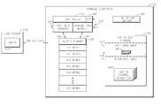
- FIG. 1is a block diagram illustrating a host system 110 connected to a storage subsystem 112 with a programmable/configurable buffer memory 126 according to one embodiment of the invention.
- the host system 110may, for example, be a portable computer, a workstation, a router, a blade server, a military system, a flight computer, or any other type of computing device.
- the host system 110stores data on the storage subsystem 112 , and may provide operating system functionality and a boot process for the storage subsystem 112 .
- the host system 110executes a driver program 113 that provides functionality for communicating with the storage subsystem 112 , such as by issuing commands in accordance with an ATA or other standard.
- the driver 113may communicate with, or be part of, one or more software applications that are specifically configured to use the storage subsystem 112 .
- the storage subsystem 112may be in the form of a detachable device, such as a solid-state memory card that plugs into a slot or external port of the host system 110 and complies with one or more of the following specifications: CompactFlash, PCMCIA, SmartMedia, MultiMediaCard, SecureDigital, Memory Stick, ATA/ATAPI, PCI Express, PCI Mezzanine Card, and AdvancedTCA Mezzanine Card.
- the storage subsystem 112comprises a controller 114 , a buffer memory 126 , and non-volatile storage 116 .
- the buffer memory 126may be internal to, or part of the same integrated circuit as, the controller 114 .
- the buffer memory 126is implemented using an array of volatile solid-state memory devices, such as static random access memory devices.
- the non-volatile storage 116is preferably implemented using solid-state memory devices, but may additionally or alternatively be implemented using magnetic disk drives, volatile memory devices (e.g., DRAM or SRAM) backed up by battery, or another type of storage device.
- the buffer memory 126operates faster than the non-volatile storage 116 , and compensates for differences in the transfer rate of data sent by host system 110 and the rate at which this data is written to the non-volatile storage 116 .
- the buffer memory 126 in the illustrated embodimentis arranged into multiple 512-byte sectors, although sectors of a larger or smaller size (e.g., 128 bytes, 256 bytes, or 1024 bytes) may alternatively be used.
- the controller 114is configured to write data to, and read data from, the non-volatile storage 116 in response to commands from the host 110 .
- the controller 114is an ATA flash disk controller that executes a firmware program which embodies the various buffer configuration features described herein. Some or all of the functions of the controller 114 may alternatively be fully automated in application-specific circuitry such that no firmware is needed.
- the controller 114is typically implemented as a single integrated circuit device, but may alternatively comprise multiple distinct devices.
- the non-volatile storage 116is subdivided into a user data area 117 and a restricted area 119 .
- the user data area 117is read/write accessible via standard (e.g. ATA) access commands, and is used by the controller 114 to implement a conventional file system (e.g., FAT16 or FAT32).
- a conventional file systeme.g., FAT16 or FAT32.
- the restricted memory area 119is preferably accessible only via one or more non-standard or “vendor-specific” commands, and thus is not exposed to the host's operating system and applications. Stated differently, the standard memory access command codes used to access the subsystem's user data memory area 117 do not provide access to the restricted area 119 .
- the restricted area 119is used to store configuration and control information, including information regarding the current configuration of the buffer memory 126 .
- the restricted memory area 119may be omitted; for example, the restricted memory area may be replaced by an internal magnetic disk drive.
- the buffer memory 126has two read/write ports 136 and 138 to efficiently move data between the host system 116 and the non-volatile storage 116 .
- the ports 136 and 138provide data channels between the buffer memory 126 and data management portions 128 and 130 of the subsystem's controller 114 . Additional read/write ports may be included; for example, a quad port SRAM may be used.
- the controller 114includes a host data manager 128 responsible for moving data to and from the host 110 .
- the host data manager 128accesses the buffer memory 126 via one of the read/write ports 136 .
- the controller 114also includes a storage data manager 130 responsible for moving data to and from the non-volatile storage 116 via the other read/write port 138 .
- the storage data manager 130may also be configured for striping data across the non-volatile storage 116 or sending the data across multiple storage read/write ports.
- the host data manager 128 and storage data manager 130may be implemented in state machine logic.
- the controller 114may also use the buffer memory 126 to implement a read buffer during read operations from the host.
- a separate, dedicated read buffermay be provided.
- the controller 114During a write operation, the controller 114 initially writes the data received from the host 110 to the buffer memory 126 , and then moves this data from the buffer memory 126 to the non-volatile storage 116 . Because the buffer memory 126 has at least two ports, the controller 114 can write to one block of the buffer memory 126 while moving data from another block of the buffer memory 126 to the non-volatile storage 116 . If no buffer memory is currently available, the controller 114 asserts a BUSY signal to the host 110 to prevent the host from sending additional write data. Thus, the controller 114 uses the BUSY signal to regulate the rate at which write data is received from the host 110 .
- the controller 114is capable of adjusting the amount of buffer memory 126 that is available to buffer write data. This is preferably accomplished by adjusting the size of a write buffer 135 implemented in the buffer memory 126 . For example, to maximize the sustained rate at which data is written to the storage subsystem 112 , the controller 114 can set the write buffer 135 to its maximum size, so that most or all of the buffer memory 126 is available for buffering write data. This setting optimizes performance, but increases the risk of data loss by increasing the amount of uncommitted data that can be stored in the volatile buffer memory 126 at a time.
- Uncommitted datarefers to write data that has not yet been written from the buffer memory to the subsystem's non-volatile storage 116 ; such data is ordinarily lost from the storage subsystem if power is lost.
- the controller 114can set the buffer size to be less than its maximum size.
- the controller 114adjusts the buffer size in response to special (non-standard) commands received from the host system 110 .
- the storage subsystem 112implements a vendor-specific command that enables the host 110 to specify the buffer size in terms of the number of 512-byte sectors it includes. For instance, if the buffer memory 126 has sixteen sectors that can be used for buffering write data, there will be sixteen possible settings (1, 2, 3 . . . 16 sectors) for the buffer size.
- the size of the write buffermay be specified in terms of a number of bytes, an address range, a set of address ranges, or some other measure. Further, as mentioned above, sectors of a different size may be used.
- the host 110may set the buffer size to a relatively small value. By doing so, the host can place an upper limit on the amount of uncommitted write data stored in the write buffer 135 at a time, and can thus limit the amount of data that will be lost if a power loss or other failure occurs. For other types of data, such as video or audio streams, the host may make the write buffer relatively large to maximize throughput.
- the controller 114may additionally or alternatively adjust the buffer size based on monitored operating conditions, such as the temperature of the storage subsystem 112 , the stability of the power signal received from the host 110 , and/or the frequency with which ECC errors are detected. Thus, in some embodiments, the storage subsystem 112 may not enable the host 110 to control the size of the buffer.
- the storage subsystem's command setalso enables the host 110 to effectively subdivide the write buffer 135 into multiple equal-size blocks 137 .
- Each blockpreferably consists of a whole number of 512-byte sectors. For example, if the buffer size is set to eight and the block size is set to two, the write buffer will be subdivided into four blocks, each of which consists of two sectors. In the example configuration shown in FIG. 1 , the buffer size is set to four sectors, and the block size is two.
- the controller 114When or shortly after a block 137 becomes full during a write operation, the controller 114 begins moving its contents to non-volatile storage 116 . If the write buffer 135 consists of a single block (i.e., the block size is equal to the buffer size), the controller asserts the BUSY signal during this move operation so that no additional write data is received from the host until the move is complete. On the other hand, if the write buffer 135 contains multiple blocks 137 , the storage subsystem/controller can receive write data into one block while moving write data from another block to non-volatile storage 116 .
- the controller 114preferably writes data to the blocks 137 , and moves data from the blocks, in a circular fashion.
- the allocation of write data to particular blocks 137occurs transparently to the host.
- Setting the block size to a relatively small valuee.g., one sector
- Setting the block size to a relatively large valuegenerally reduces the data transfer delay between the host system 110 and the receipt of data into the write buffer 135 .
- the storage subsystem 112may alternatively be implemented without subdividing the write buffer 135 into multiple blocks.
- the storage subsystemcan be implemented such that the number of blocks, and/or the size of each block, is fixed.
- the controller 114preferably implements multiple modes of operation that define how the buffer size, or the buffer size and block size, can be varied. These modes may, for example, include Automatic Mode, Host Set Mode, and Monitor Mode, as discussed below, although these particular modes are not required.
- the host system 110can place the storage subsystem into a desired mode using a vendor-specific command.
- the restricted memory area 119 of the storage subsystem 112preferably stores buffer control parameters 140 that indicate the current configuration of the write buffer, including, e.g., the buffer size and block size settings and/or the current mode setting. This enables the controller 114 to restore these settings when the subsystem 112 is powered up.
- the controller 114may also effectively cache the buffer control parameters in its register storage.
- the control parameters 140are stored in a restricted 512-byte block of the non-volatile storage 116 in a preconfigured location and format known to the controller 114 .
- the host system 110may execute software, such as the driver 113 , that is configured to use the appropriate vendor-specific command or commands to control the configuration of the write buffer 135 and the associated mode of operation.
- the restricted memory area 119may also be used by the controller 114 to store other types of control information.
- the restricted memory area 119may store firmware executed by the controller 114 , security information for controlling access to the user data area 117 , and/or wear level data reflective of the wear level of each sector of the non-volatile storage 116 .
- FIG. 2is a flow chart illustrating generally how the storage subsystem 112 configures and uses the buffer memory 126 when connected to a host 110 .
- a subsystem 112 containing buffer control parameters 140 in its restricted memory area 119is connected to a host system 110 .
- the subsystem 112is a USB-based flash memory drive
- the flash drivemay be connected to a USB port of the host system 110 .
- step 202when the storage subsystem 112 powers up, the controller 114 reads the buffer control parameters 140 from the non-volatile storage 116 .
- the controller 114thereafter maintains the retrieved buffer control parameters 140 in volatile register storage, and uses the buffer memory 126 to cache write data in accordance with these settings.
- This sectiondescribes one example of a set of modes that may be implemented by the storage subsystem 112 to flexibly control how the buffer memory 126 is configured and used. As will be recognized, the subsystem 112 can be implemented without these modes.
- the controller 114When in Automatic Mode, the controller 114 automatically adjusts the block size (transparently to the host) based on the transfer command received from the host system 110 .
- the storage subsystem 112may thus advantageously internally adjust the block size to increase the speed of the data transfer between the host system 110 and the storage subsystem 112 , and to optimize the data transfer rate/data integrity tradeoff accordingly.
- the controller 114may use this value to select the appropriate block size for the transfer. For instance, if the Sector Count Register field is set to “02h” in the command, the controller 114 would use a block size of two. If, however, the host write command indicates a transfer of six sectors (e.g. the Sector Count Register field is “06h”), the controller 114 would set the block size to six sectors. The controller may also appropriately adjust the buffer size to accommodate the changes in block size.
- the host system 110can set or change the buffer size and block size.
- the host system 110may, for example, adjust these parameters based on the conditions surrounding the host system 110 , such as the criticality of the data being stored and/or the susceptibility of the subsystem 112 to power loss or other failure.
- the host 110may maintain a log of events in which the subsystem 112 is connected and disconnected. The host may then use this log to calculate a probability that the subsystem will be disconnected from the host during a write operation, and may use this probability value to configure the buffer so as to stay within a pre-specified risk level.
- the storage subsystem 112may be placed in the Host Set Mode using a vendor-specific command that includes a first field to designate the buffer mode, and which includes two additional fields that specify the buffer size and block size, respectfully, when the Host Set Mode is specified by the first field. These settings are recorded persistently via the buffer control parameters 140 , and are used until changed via another vendor-specific command.
- the storage subsystem 112is operating in the Host Set Mode. If the block size is set to two and the buffer size is set to four or more, the subsystem will use two 2-sector blocks to handle the transfer. If, on the other hand, both the block size and the buffer size are set to two, the subsystem will use a 2-sector block to handle the first half of the transfer, and will then use the same 2-sector block to handle the second half of the transfer.
- the Host Set Modemay be used to manage the risk of data loss.
- the subsystem 112may store heart monitoring data from a heart monitoring host system 110 , and that data may be read and analyzed by a separate personal computer system (not shown). With the surrounding conditions of battery operation, possibility of power loss, and the transfer of critical data, the host system 110 may set the buffer size to one sector so that the amount of uncommitted heart monitoring data in the write buffer at any give time will be relatively small. When heart monitor logging is completed, the storage subsystem 112 may then be connected to the personal computer system for data analysis.
- the new conditions surrounding the personal computer systemare typically a low probability of data loss, mostly read operations with very few write operations, and large amounts of data being read. Consequently, the host may increase the size of the write buffer to enable writes to occur at higher speeds.
- the subsystem's controller 114can automatically adjust the buffer parameters based on data reflective of whether a power loss or other failure will likely occur. For example, the controller 114 may select the appropriate buffer size (and optionally block size) based on any one or more of the following: (a) the temperature of the storage subsystem, (b) the length of time that the subsystem 112 has been powered up, (c) the average length of time that the subsystem 112 remains powered up; (d) the length of time since the last power signal anomaly was detected, (e) the percentage of time in which the power signal has been anomalous since the last power-up; (f) the percentage of time spent executing write operations since the last power-up; (g) the percentage of sectors in which ECC errors have been detected on read operations, (h) the output of an internal shock or vibration sensor, (i) usage statistics reflective of the wear state, and thus the expected remaining life, of the non-volatile memory array, as generated, e.g., as described in U.S.
- the controller 114may maintain these and other types of data in the restricted memory area 119 , and may analyze the collected data to predict likelihoods of failure. When the risk of a failure is relatively high, a relatively small buffer size may be used. When the risk of a failure is relatively low, a relatively large buffer size may be used.
- the controller 114may adjust the buffer size based partly or wholly on temperature readings taken from a temperature sensor 160 incorporated into the subsystem 112 .
- the temperature sensor 160may be connected to an analog-to-digital converter 162 of the controller 114 as shown, or to an external analog-to-digital converter.
- the subsystem controller 114may, for example, decrease the buffer size when the temperature of the storage subsystem 112 exceeds 80 degrees Celsius, which may be indicative of an increased likelihood of system failure.
- the controller 114may monitor power conditions, and may adjust the buffer size based on power supply noise or level thresholds indicative of potential power loss. For example, the controller 114 may decrease the buffer size when the power supply noise measurements exceed 100 mV, or when the power signal drops below some threshold.
- the storage subsystem 112may include a battery that is used as a backup power source such that write operations can be completed if power from the host is lost.
- the controller 114may adjust the buffer size based on the charge status of the battery. For example, the controller 114 may decrease the buffer size when the battery's charge level falls below a selected threshold.
- the storage subsystem 112may adjust the buffer size to match the cluster size (the minimum size block of data that a file system can write) of the host system data partition for optimized synchronization with the host system's 110 file system.
- the controller 114may adjust the buffer size based on a combination of environmental and system variables. For example, the controller 114 may decrease the buffer size when the temperature increases beyond a given threshold, the power supply noise exceeds a given threshold, or both the temperature and power supply noise exceed some lower thresholds. Further, the controller 114 may use a number of different factors (such as those enumerated above) to calculate a probability of power loss, and may then use this probability value to select an appropriate buffer size.
- the storage subsystem 112may be a solid-state memory card or drive that plugs into a slot or port of the host system 110 , and may comply with one of the following card specifications: CompactFlash, PCMCIA, SmartMedia, MultiMediaCard, SecureDigital, Memory Stick, ATA/ATAPI, PCI Express, PCI Mezzanine Card, and AdvancedTCA Mezzanine Card.
- the storage subsystem 112may also have a housing and signal interface that complies with one of the following specifications: sub 1 inch hard disk drive, 1.8 inch hard disk drive, 2.5 inch hard disk drive and 3.5 inch hard disk drive. A custom form factor and/or signal interface may alternatively be used.
- the storage subsystem 112typically includes a physical connector for attaching to the host 110 , the storage subsystem 112 may alternatively communication with the host via a wireless interface such as Bluetooth or IEEE-802.11.
- the controller 114comprises an ATA flash disk controller that executes firmware.
- the firmware executed by the controller 114embodies functionality for implementing the features described herein, including providing access to the restricted memory area 119 via vendor-specific commands.
- the controller 114may alternatively be implemented in-whole or in-part as an ASIC, FPGA, or other device, which may but need not execute firmware.
- the non-volatile storage 116may, but need not, be implemented using NAND memory components.
- the non-volatile storage 116may comprise a plurality of solid-state storage devices coupled to the controller 114 .
- the non-volatile storage 116may comprise, for example, flash integrated circuits, Chalcogenide RAM (C-RAM), Phase Change Memory (PC-RAM or PRAM), Programmable Metallization Cell RAM (PMC-RAM or PMCm), Ovonic Unified Memory (OUM), Resistance RAM (RRAM), NAND memory, NOR memory, EEPROM, Ferroelectric Memory (FeRAM), or other discrete NVM chips.
- the solid-state storage devicesmay be physically divided into blocks, pages and sectors, as is known in the art.
- other forms of non-volatile storagee.g., battery backed-up volatile DRAM or SRAM devices, magnetic disk drives, etc. may additionally or alternatively be used.
Landscapes
- Engineering & Computer Science (AREA)
- Theoretical Computer Science (AREA)
- Human Computer Interaction (AREA)
- Physics & Mathematics (AREA)
- General Engineering & Computer Science (AREA)
- General Physics & Mathematics (AREA)
- Techniques For Improving Reliability Of Storages (AREA)
Abstract
Description
Claims (20)
Priority Applications (1)
| Application Number | Priority Date | Filing Date | Title |
|---|---|---|---|
| US12/566,453US8151020B2 (en) | 2007-02-07 | 2009-09-24 | Storage subsystem with configurable buffer |
Applications Claiming Priority (2)
| Application Number | Priority Date | Filing Date | Title |
|---|---|---|---|
| US11/672,435US7596643B2 (en) | 2007-02-07 | 2007-02-07 | Storage subsystem with configurable buffer |
| US12/566,453US8151020B2 (en) | 2007-02-07 | 2009-09-24 | Storage subsystem with configurable buffer |
Related Parent Applications (1)
| Application Number | Title | Priority Date | Filing Date |
|---|---|---|---|
| US11/672,435ContinuationUS7596643B2 (en) | 2007-02-07 | 2007-02-07 | Storage subsystem with configurable buffer |
Publications (2)
| Publication Number | Publication Date |
|---|---|
| US20100017542A1 US20100017542A1 (en) | 2010-01-21 |
| US8151020B2true US8151020B2 (en) | 2012-04-03 |
Family
ID=39677139
Family Applications (2)
| Application Number | Title | Priority Date | Filing Date |
|---|---|---|---|
| US11/672,435Active2027-06-04US7596643B2 (en) | 2007-02-07 | 2007-02-07 | Storage subsystem with configurable buffer |
| US12/566,453Expired - Fee RelatedUS8151020B2 (en) | 2007-02-07 | 2009-09-24 | Storage subsystem with configurable buffer |
Family Applications Before (1)
| Application Number | Title | Priority Date | Filing Date |
|---|---|---|---|
| US11/672,435Active2027-06-04US7596643B2 (en) | 2007-02-07 | 2007-02-07 | Storage subsystem with configurable buffer |
Country Status (3)
| Country | Link |
|---|---|
| US (2) | US7596643B2 (en) |
| EP (1) | EP2165262B1 (en) |
| WO (1) | WO2008097764A1 (en) |
Cited By (127)
| Publication number | Priority date | Publication date | Assignee | Title |
|---|---|---|---|---|
| US8312207B2 (en) | 2006-05-08 | 2012-11-13 | Siliconsystems, Inc. | Systems and methods for measuring the useful life of solid-state storage devices |
| US20130159797A1 (en)* | 2011-12-20 | 2013-06-20 | Sandisk Technologies Inc. | Apparatus and methods for indicating the health of removable storage devices |
| US20130223419A1 (en)* | 2012-02-29 | 2013-08-29 | Nokia Corporation | Method, apparatus, and computer program product for power saving enhancements in wireless communication |
| US8549236B2 (en) | 2006-12-15 | 2013-10-01 | Siliconsystems, Inc. | Storage subsystem with multiple non-volatile memory arrays to protect against data losses |
| US8898373B1 (en) | 2011-06-29 | 2014-11-25 | Western Digital Technologies, Inc. | System and method for improving wear-leveling performance in solid-state memory |
| US8917471B1 (en) | 2013-10-29 | 2014-12-23 | Western Digital Technologies, Inc. | Power management for data storage device |
| US8954655B2 (en) | 2013-01-14 | 2015-02-10 | Western Digital Technologies, Inc. | Systems and methods of configuring a mode of operation in a solid-state memory |
| US8954653B1 (en) | 2012-06-26 | 2015-02-10 | Western Digital Technologies, Inc. | Mechanisms for efficient management of system data in data storage systems |
| US8954694B2 (en) | 2012-11-15 | 2015-02-10 | Western Digital Technologies, Inc. | Methods, data storage devices and systems for fragmented firmware table rebuild in a solid state drive |
| US8959284B1 (en) | 2010-06-28 | 2015-02-17 | Western Digital Technologies, Inc. | Disk drive steering write data to write cache based on workload |
| US8959416B1 (en) | 2011-12-16 | 2015-02-17 | Western Digital Technologies, Inc. | Memory defect management using signature identification |
| US8966343B2 (en) | 2012-08-21 | 2015-02-24 | Western Digital Technologies, Inc. | Solid-state drive retention monitor using reference blocks |
| US8966205B1 (en) | 2012-05-10 | 2015-02-24 | Western Digital Technologies, Inc. | System data management using garbage collection and hybrid self mapping |
| US8966339B1 (en) | 2012-12-18 | 2015-02-24 | Western Digital Technologies, Inc. | Decoder supporting multiple code rates and code lengths for data storage systems |
| US8972655B2 (en) | 2013-01-21 | 2015-03-03 | Western Digital Technolgies, Inc. | Initialization of a storage device |
| US8972826B2 (en) | 2012-10-24 | 2015-03-03 | Western Digital Technologies, Inc. | Adaptive error correction codes for data storage systems |
| US8977804B1 (en) | 2011-11-21 | 2015-03-10 | Western Digital Technologies, Inc. | Varying data redundancy in storage systems |
| US8984247B1 (en) | 2012-05-10 | 2015-03-17 | Western Digital Technologies, Inc. | Storing and reconstructing mapping table data in a data storage system |
| US8990668B2 (en) | 2013-03-14 | 2015-03-24 | Western Digital Technologies, Inc. | Decoding data stored in solid-state memory |
| US9007854B1 (en) | 2013-12-09 | 2015-04-14 | Western Digital Technologies, Inc. | Method and system for optimized soft decoding in a data storage device |
| US9007841B1 (en) | 2013-10-24 | 2015-04-14 | Western Digital Technologies, Inc. | Programming scheme for improved voltage distribution in solid-state memory |
| US9013920B2 (en) | 2013-04-03 | 2015-04-21 | Western Digital Technologies, Inc. | Systems and methods of write precompensation to extend life of a solid-state memory |
| US9021192B1 (en) | 2010-09-21 | 2015-04-28 | Western Digital Technologies, Inc. | System and method for enhancing processing of memory access requests |
| US9021339B2 (en) | 2012-11-29 | 2015-04-28 | Western Digital Technologies, Inc. | Data reliability schemes for data storage systems |
| US9021168B1 (en) | 2011-09-06 | 2015-04-28 | Western Digital Technologies, Inc. | Systems and methods for an enhanced controller architecture in data storage systems |
| US9026716B2 (en) | 2010-05-12 | 2015-05-05 | Western Digital Technologies, Inc. | System and method for managing garbage collection in solid-state memory |
| US9032271B2 (en) | 2012-12-07 | 2015-05-12 | Western Digital Technologies, Inc. | System and method for lower page data recovery in a solid state drive |
| US9036283B1 (en) | 2014-01-22 | 2015-05-19 | Western Digital Technologies, Inc. | Data storage device with selective write to a first storage media or a second storage media |
| US9042197B2 (en) | 2013-07-23 | 2015-05-26 | Western Digital Technologies, Inc. | Power fail protection and recovery using low power states in a data storage device/system |
| US9053008B1 (en) | 2012-03-26 | 2015-06-09 | Western Digital Technologies, Inc. | Systems and methods for providing inline parameter service in data storage devices |
| US9059736B2 (en) | 2012-12-03 | 2015-06-16 | Western Digital Technologies, Inc. | Methods, solid state drive controllers and data storage devices having a runtime variable raid protection scheme |
| US9058261B1 (en) | 2011-09-06 | 2015-06-16 | Western Digital Technologies, Inc. | Systems and methods for detailed error reporting in data storage systems |
| US9058280B1 (en) | 2010-08-13 | 2015-06-16 | Western Digital Technologies, Inc. | Hybrid drive migrating data from disk to non-volatile semiconductor memory based on accumulated access time |
| US9059742B1 (en) | 2013-03-15 | 2015-06-16 | Western Digital Technologies, Inc. | System and method for dynamic scaling of LDPC decoder in a solid state drive |
| US9069475B1 (en) | 2010-10-26 | 2015-06-30 | Western Digital Technologies, Inc. | Hybrid drive selectively spinning up disk when powered on |
| US9070379B2 (en) | 2013-08-28 | 2015-06-30 | Western Digital Technologies, Inc. | Data migration for data storage device |
| US9081700B2 (en) | 2013-05-16 | 2015-07-14 | Western Digital Technologies, Inc. | High performance read-modify-write system providing line-rate merging of dataframe segments in hardware |
| US9092146B2 (en) | 2013-06-28 | 2015-07-28 | International Business Machines Corporation | Dynamically varying transfer size in a storage device for improved performance |
| US9110835B1 (en) | 2011-03-09 | 2015-08-18 | Western Digital Technologies, Inc. | System and method for improving a data redundancy scheme in a solid state subsystem with additional metadata |
| US9123686B2 (en) | 2013-04-12 | 2015-09-01 | Western Digital Technologies, Inc. | Thermal management for solid-state drive |
| US9122625B1 (en) | 2012-12-18 | 2015-09-01 | Western Digital Technologies, Inc. | Error correcting code encoder supporting multiple code rates and throughput speeds for data storage systems |
| US9141176B1 (en) | 2013-07-29 | 2015-09-22 | Western Digital Technologies, Inc. | Power management for data storage device |
| US9164886B1 (en) | 2010-09-21 | 2015-10-20 | Western Digital Technologies, Inc. | System and method for multistage processing in a memory storage subsystem |
| US9170938B1 (en) | 2013-05-17 | 2015-10-27 | Western Digital Technologies, Inc. | Method and system for atomically writing scattered information in a solid state storage device |
| US9170932B1 (en) | 2012-05-22 | 2015-10-27 | Western Digital Technologies, Inc. | System data storage mechanism providing coherency and segmented data loading |
| US9177638B2 (en) | 2012-11-13 | 2015-11-03 | Western Digital Technologies, Inc. | Methods and devices for avoiding lower page corruption in data storage devices |
| US9176859B2 (en) | 2009-01-07 | 2015-11-03 | Siliconsystems, Inc. | Systems and methods for improving the performance of non-volatile memory operations |
| US9182916B1 (en) | 2010-09-17 | 2015-11-10 | Western Digital Technologies, Inc. | Non-volatile storage subsystem with energy-based performance throttling |
| US9195293B1 (en) | 2013-05-03 | 2015-11-24 | Western Digital Technologies, Inc. | User controlled data storage device power and performance settings |
| US9195530B1 (en) | 2011-09-06 | 2015-11-24 | Western Digital Technologies, Inc. | Systems and methods for improved data management in data storage systems |
| US9208101B2 (en) | 2013-06-26 | 2015-12-08 | Western Digital Technologies, Inc. | Virtual NAND capacity extension in a hybrid drive |
| US9208020B2 (en) | 2012-06-26 | 2015-12-08 | Western Digital Technologies, Inc. | Efficient error handling mechanisms in data storage systems |
| US9214963B1 (en) | 2012-12-21 | 2015-12-15 | Western Digital Technologies, Inc. | Method and system for monitoring data channel to enable use of dynamically adjustable LDPC coding parameters in a data storage system |
| US9218279B2 (en) | 2013-03-15 | 2015-12-22 | Western Digital Technologies, Inc. | Atomic write command support in a solid state drive |
| US9250994B1 (en) | 2014-02-05 | 2016-02-02 | Western Digital Technologies, Inc. | Non-binary low-density parity check (LDPC) decoding using trellis maximization |
| US9263136B1 (en) | 2013-09-04 | 2016-02-16 | Western Digital Technologies, Inc. | Data retention flags in solid-state drives |
| US9268701B1 (en) | 2011-11-21 | 2016-02-23 | Western Digital Technologies, Inc. | Caching of data in data storage systems by managing the size of read and write cache based on a measurement of cache reliability |
| US9268487B2 (en) | 2014-03-24 | 2016-02-23 | Western Digital Technologies, Inc. | Method and apparatus for restricting writes to solid state memory when an end-of life condition is reached |
| US9270296B1 (en) | 2013-11-13 | 2016-02-23 | Western Digital Technologies, Inc. | Method and system for soft decoding through single read |
| US9275741B1 (en) | 2014-09-10 | 2016-03-01 | Western Digital Technologies, Inc. | Temperature compensation management in solid-state memory |
| US9274978B2 (en) | 2013-06-10 | 2016-03-01 | Western Digital Technologies, Inc. | Migration of encrypted data for data storage systems |
| US9274966B1 (en) | 2013-02-20 | 2016-03-01 | Western Digital Technologies, Inc. | Dynamically throttling host commands to disk drives |
| US9280472B1 (en) | 2013-03-13 | 2016-03-08 | Western Digital Technologies, Inc. | Caching data in a high performance zone of a data storage system |
| US9280200B1 (en) | 2013-05-20 | 2016-03-08 | Western Digital Technologies, Inc. | Automatic peak current throttle of tiered storage elements |
| US9286176B1 (en) | 2013-11-08 | 2016-03-15 | Western Digital Technologies, Inc. | Selective skipping of blocks in an SSD |
| US9304709B2 (en) | 2013-09-06 | 2016-04-05 | Western Digital Technologies, Inc. | High performance system providing selective merging of dataframe segments in hardware |
| US9304560B2 (en) | 2013-06-19 | 2016-04-05 | Western Digital Technologies, Inc. | Backup power for reducing host current transients |
| US9323467B2 (en) | 2013-10-29 | 2016-04-26 | Western Digital Technologies, Inc. | Data storage device startup |
| US9330143B2 (en) | 2013-10-24 | 2016-05-03 | Western Digital Technologies, Inc. | Data storage device supporting accelerated database operations |
| US9337864B1 (en) | 2014-01-29 | 2016-05-10 | Western Digital Technologies, Inc. | Non-binary LDPC decoder using binary subgroup processing |
| US9338927B2 (en) | 2013-05-02 | 2016-05-10 | Western Digital Technologies, Inc. | Thermal interface material pad and method of forming the same |
| US9335950B2 (en) | 2013-03-15 | 2016-05-10 | Western Digital Technologies, Inc. | Multiple stream compression and formatting of data for data storage systems |
| US9335945B2 (en) | 2014-06-10 | 2016-05-10 | International Business Machines Corporation | Transfer size monitor, determination, and optimization engine for storage devices |
| US9348520B2 (en) | 2014-03-24 | 2016-05-24 | Western Digital Technologies, Inc. | Lifetime extension of non-volatile semiconductor memory for data storage device |
| US9348741B1 (en) | 2011-12-19 | 2016-05-24 | Western Digital Technologies, Inc. | Systems and methods for handling write data access requests in data storage devices |
| US9354955B1 (en) | 2014-03-19 | 2016-05-31 | Western Digital Technologies, Inc. | Partial garbage collection for fast error handling and optimized garbage collection for the invisible band |
| US9361044B2 (en) | 2011-03-28 | 2016-06-07 | Western Digital Technologies, Inc. | Power-safe data management system |
| US9384088B1 (en) | 2014-02-24 | 2016-07-05 | Western Digital Technologies, Inc. | Double writing map table entries in a data storage system to guard against silent corruption |
| US9405675B1 (en) | 2010-05-11 | 2016-08-02 | Western Digital Technologies, Inc. | System and method for managing execution of internal commands and host commands in a solid-state memory |
| US9405356B1 (en) | 2014-10-21 | 2016-08-02 | Western Digital Technologies, Inc. | Temperature compensation in data storage device |
| US9405617B1 (en) | 2011-02-11 | 2016-08-02 | Western Digital Technologies, Inc. | System and method for data error recovery in a solid state subsystem |
| US9418699B1 (en) | 2014-10-09 | 2016-08-16 | Western Digital Technologies, Inc. | Management of sequentially written data |
| US9436630B2 (en) | 2013-06-11 | 2016-09-06 | Western Digital Technologies, Inc. | Using dual phys to support multiple PCIe link widths |
| US9442668B1 (en) | 2013-08-29 | 2016-09-13 | Western Digital Technologies, Inc. | Adaptive power management control with performance feedback |
| US9448742B2 (en) | 2014-03-27 | 2016-09-20 | Western Digital Technologies, Inc. | Communication between a host and a secondary storage device |
| US9448738B2 (en) | 2013-03-15 | 2016-09-20 | Western Digital Technologies, Inc. | Compression and formatting of data for data storage systems |
| US9454474B2 (en) | 2013-03-05 | 2016-09-27 | Western Digital Technologies, Inc. | Methods, devices and systems for two stage power-on map rebuild with free space accounting in a solid state drive |
| US9472222B2 (en) | 2014-05-16 | 2016-10-18 | Western Digital Technologies, Inc. | Vibration mitigation for a data storage device |
| US9489296B1 (en) | 2012-10-17 | 2016-11-08 | Western Digital Technologies, Inc. | Methods, devices and systems for hardware-based garbage collection in solid state drives |
| US9507523B1 (en) | 2012-10-12 | 2016-11-29 | Western Digital Technologies, Inc. | Methods, devices and systems for variable size logical page management in a solid state drive |
| US9529710B1 (en) | 2013-12-06 | 2016-12-27 | Western Digital Technologies, Inc. | Interleaved channels in a solid-state drive |
| US9542287B1 (en) | 2011-09-06 | 2017-01-10 | Western Digital Technologies, Inc. | Systems and methods for error injection in data storage systems |
| US9564212B2 (en) | 2014-05-06 | 2017-02-07 | Western Digital Technologies, Inc. | Solid-state memory corruption mitigation |
| US9583153B1 (en) | 2013-06-28 | 2017-02-28 | Western Digital Technologies, Inc. | Memory card placement within a solid state drive |
| US9619317B1 (en) | 2012-12-18 | 2017-04-11 | Western Digital Technologies, Inc. | Decoder having early decoding termination detection |
| US9620226B1 (en) | 2015-10-30 | 2017-04-11 | Western Digital Technologies, Inc. | Data retention charge loss and read disturb compensation in solid-state data storage systems |
| US9641378B1 (en) | 2013-03-12 | 2017-05-02 | Western Digital Technologies, Inc. | Adjustment of compression ratios for data storage |
| US9652379B1 (en) | 2010-09-15 | 2017-05-16 | Western Digital Technologies, Inc. | System and method for reducing contentions in solid-state memory access |
| US9668337B2 (en) | 2015-09-08 | 2017-05-30 | Western Digital Technologies, Inc. | Temperature management in data storage devices |
| US9665501B1 (en) | 2013-06-18 | 2017-05-30 | Western Digital Technologies, Inc. | Self-encrypting data storage device supporting object-level encryption |
| US9690696B1 (en) | 2014-05-14 | 2017-06-27 | Western Digital Technologies, Inc. | Lifetime extension of memory for data storage system |
| US9727261B2 (en) | 2015-09-24 | 2017-08-08 | Western Digital Technologies, Inc. | Weighted programming patterns in solid-state data storage systems |
| US9740248B2 (en) | 2013-06-07 | 2017-08-22 | Western Digital Technologies, Inc. | Component placement within a solid state drive |
| US9753847B2 (en) | 2009-10-27 | 2017-09-05 | Western Digital Technologies, Inc. | Non-volatile semiconductor memory segregating sequential, random, and system data to reduce garbage collection for page based mapping |
| US9785563B1 (en) | 2015-08-13 | 2017-10-10 | Western Digital Technologies, Inc. | Read command processing for data storage system based on previous writes |
| US9823859B2 (en) | 2014-11-06 | 2017-11-21 | Western Digital Technologies, Inc. | Mechanical shock mitigation for data storage |
| US9830257B1 (en) | 2013-06-12 | 2017-11-28 | Western Digital Technologies, Inc. | Fast saving of data during power interruption in data storage systems |
| US9836220B2 (en) | 2014-10-20 | 2017-12-05 | Samsung Electronics Co., Ltd. | Data processing system and method of operating the same |
| US9836232B1 (en) | 2015-09-30 | 2017-12-05 | Western Digital Technologies, Inc. | Data storage device and method for using secondary non-volatile memory for temporary metadata storage |
| US9857995B1 (en) | 2015-03-09 | 2018-01-02 | Western Digital Technologies, Inc. | Data storage device and method providing non-volatile memory buffer for real-time primary non-volatile memory protection |
| US9977612B1 (en) | 2012-05-11 | 2018-05-22 | Western Digital Technologies, Inc. | System data management using garbage collection and logs |
| US10013174B2 (en) | 2015-09-30 | 2018-07-03 | Western Digital Technologies, Inc. | Mapping system selection for data storage device |
| US10079048B2 (en) | 2009-03-24 | 2018-09-18 | Western Digital Technologies, Inc. | Adjusting access of non-volatile semiconductor memory based on access time |
| US10126981B1 (en) | 2015-12-14 | 2018-11-13 | Western Digital Technologies, Inc. | Tiered storage using storage class memory |
| US10140067B1 (en) | 2013-12-19 | 2018-11-27 | Western Digital Technologies, Inc. | Data management for data storage device with multiple types of non-volatile memory media |
| US10387303B2 (en) | 2016-08-16 | 2019-08-20 | Western Digital Technologies, Inc. | Non-volatile storage system with compute engine to accelerate big data applications |
| US10417123B1 (en) | 2013-05-16 | 2019-09-17 | Western Digital Technologies, Inc. | Systems and methods for improving garbage collection and wear leveling performance in data storage systems |
| US10444998B1 (en) | 2013-10-24 | 2019-10-15 | Western Digital Technologies, Inc. | Data storage device providing data maintenance services |
| US10459644B2 (en) | 2016-10-28 | 2019-10-29 | Western Digital Techologies, Inc. | Non-volatile storage system with integrated compute engine and optimized use of local fast memory |
| US10545819B1 (en) | 2013-03-12 | 2020-01-28 | Western Digital Technologies, Inc. | Soft-decision input generation for data storage systems |
| US10565123B2 (en) | 2017-04-10 | 2020-02-18 | Western Digital Technologies, Inc. | Hybrid logical to physical address translation for non-volatile storage devices with integrated compute module |
| US10740231B2 (en) | 2018-11-20 | 2020-08-11 | Western Digital Technologies, Inc. | Data access in data storage device including storage class memory |
| US10769062B2 (en) | 2018-10-01 | 2020-09-08 | Western Digital Technologies, Inc. | Fine granularity translation layer for data storage devices |
| US10956071B2 (en) | 2018-10-01 | 2021-03-23 | Western Digital Technologies, Inc. | Container key value store for data storage devices |
| US11016905B1 (en) | 2019-11-13 | 2021-05-25 | Western Digital Technologies, Inc. | Storage class memory access |
| US11249921B2 (en) | 2020-05-06 | 2022-02-15 | Western Digital Technologies, Inc. | Page modification encoding and caching |
| US12217797B2 (en) | 2021-11-03 | 2025-02-04 | Samsung Electronics Co., Ltd. | Storage device and operating method thereof |
Families Citing this family (153)
| Publication number | Priority date | Publication date | Assignee | Title |
|---|---|---|---|---|
| US7427027B2 (en)* | 2004-07-28 | 2008-09-23 | Sandisk Corporation | Optimized non-volatile storage systems |
| JP5032172B2 (en)* | 2007-03-28 | 2012-09-26 | 株式会社東芝 | Integrated memory management apparatus and method, and data processing system |
| US8135900B2 (en)* | 2007-03-28 | 2012-03-13 | Kabushiki Kaisha Toshiba | Integrated memory management and memory management method |
| JP2008287600A (en)* | 2007-05-18 | 2008-11-27 | Seiko Epson Corp | HOST DEVICE, INFORMATION PROCESSING DEVICE, ELECTRONIC DEVICE, PROGRAM, AND READ CONTROL METHOD |
| US8762620B2 (en)* | 2007-12-27 | 2014-06-24 | Sandisk Enterprise Ip Llc | Multiprocessor storage controller |
| US8892831B2 (en)* | 2008-01-16 | 2014-11-18 | Apple Inc. | Memory subsystem hibernation |
| US20090198952A1 (en)* | 2008-02-04 | 2009-08-06 | Apple Inc | Memory Mapping Architecture |
| US8332572B2 (en) | 2008-02-05 | 2012-12-11 | Spansion Llc | Wear leveling mechanism using a DRAM buffer |
| US8209463B2 (en)* | 2008-02-05 | 2012-06-26 | Spansion Llc | Expansion slots for flash memory based random access memory subsystem |
| US8352671B2 (en) | 2008-02-05 | 2013-01-08 | Spansion Llc | Partial allocate paging mechanism using a controller and a buffer |
| US8275945B2 (en)* | 2008-02-05 | 2012-09-25 | Spansion Llc | Mitigation of flash memory latency and bandwidth limitations via a write activity log and buffer |
| US20090216942A1 (en)* | 2008-02-23 | 2009-08-27 | Broadcom Corporation | Efficient memory management for hard disk drive (hdd) read channel |
| US20090307409A1 (en)* | 2008-06-06 | 2009-12-10 | Apple Inc. | Device memory management |
| JP5244037B2 (en)* | 2008-07-15 | 2013-07-24 | パナソニック株式会社 | Memory device, memory device controller |
| JP5216463B2 (en)* | 2008-07-30 | 2013-06-19 | 株式会社日立製作所 | Storage device, storage area management method thereof, and flash memory package |
| US8516219B2 (en)* | 2009-07-24 | 2013-08-20 | Apple Inc. | Index cache tree |
| US8468293B2 (en)* | 2009-07-24 | 2013-06-18 | Apple Inc. | Restore index page |
| US8365041B2 (en) | 2010-03-17 | 2013-01-29 | Sandisk Enterprise Ip Llc | MLC self-raid flash data protection scheme |
| US8495757B2 (en) | 2010-04-22 | 2013-07-23 | Hewlett-Packard Development Company, L.P. | System and method for placing an electronic apparatus into a protected state in response to environmental data |
| US9009406B2 (en) | 2010-12-10 | 2015-04-14 | International Business Machines Corporation | Determining server write activity levels to use to adjust write cache size |
| US8775847B2 (en)* | 2010-12-14 | 2014-07-08 | Memory Technologies Llc | Method and apparatus to boost mass memory performance given power supply availability |
| US8374040B2 (en) | 2011-02-25 | 2013-02-12 | International Business Machines Corporation | Write bandwidth in a memory characterized by a variable write time |
| WO2012124117A1 (en)* | 2011-03-17 | 2012-09-20 | 富士通株式会社 | Timing error elimination method, design assistance device, and program |
| US8910020B2 (en) | 2011-06-19 | 2014-12-09 | Sandisk Enterprise Ip Llc | Intelligent bit recovery for flash memory |
| US8909982B2 (en) | 2011-06-19 | 2014-12-09 | Sandisk Enterprise Ip Llc | System and method for detecting copyback programming problems |
| KR20130000963A (en)* | 2011-06-24 | 2013-01-03 | 삼성전자주식회사 | Semiconductor storage system |
| JP5791397B2 (en)* | 2011-07-07 | 2015-10-07 | ルネサスエレクトロニクス株式会社 | Device controller, USB device controller, and power control method |
| JP2014522066A (en)* | 2011-08-09 | 2014-08-28 | エルエスアイ コーポレーション | Interoperation of I/O devices with computing hosts |
| WO2013054374A1 (en)* | 2011-10-12 | 2013-04-18 | Hitachi, Ltd. | Storage system, and data backup method and system restarting method of storage system |
| TW201317787A (en)* | 2011-10-27 | 2013-05-01 | Chung Shan Inst Of Science | Extended battery management system |
| US8938658B2 (en) | 2011-11-07 | 2015-01-20 | Sandisk Enterprise Ip Llc | Statistical read comparison signal generation for memory systems |
| US8954822B2 (en) | 2011-11-18 | 2015-02-10 | Sandisk Enterprise Ip Llc | Data encoder and decoder using memory-specific parity-check matrix |
| US8924815B2 (en) | 2011-11-18 | 2014-12-30 | Sandisk Enterprise Ip Llc | Systems, methods and devices for decoding codewords having multiple parity segments |
| US9048876B2 (en) | 2011-11-18 | 2015-06-02 | Sandisk Enterprise Ip Llc | Systems, methods and devices for multi-tiered error correction |
| US20130151755A1 (en) | 2011-12-12 | 2013-06-13 | Reuven Elhamias | Non-Volatile Storage Systems with Go To Sleep Adaption |
| US9699263B1 (en) | 2012-08-17 | 2017-07-04 | Sandisk Technologies Llc. | Automatic read and write acceleration of data accessed by virtual machines |
| US9009566B2 (en)* | 2012-09-12 | 2015-04-14 | Macronix International Co., Ltd. | Outputting information of ECC corrected bits |
| US9852140B1 (en)* | 2012-11-07 | 2017-12-26 | Axcient, Inc. | Efficient file replication |
| KR101934519B1 (en)* | 2012-11-26 | 2019-01-02 | 삼성전자주식회사 | Storage device and data transfering method thereof |
| US9329666B2 (en)* | 2012-12-21 | 2016-05-03 | Advanced Micro Devices, Inc. | Power throttling queue |
| US9501398B2 (en) | 2012-12-26 | 2016-11-22 | Sandisk Technologies Llc | Persistent storage device with NVRAM for staging writes |
| US9612948B2 (en) | 2012-12-27 | 2017-04-04 | Sandisk Technologies Llc | Reads and writes between a contiguous data block and noncontiguous sets of logical address blocks in a persistent storage device |
| US9239751B1 (en) | 2012-12-27 | 2016-01-19 | Sandisk Enterprise Ip Llc | Compressing data from multiple reads for error control management in memory systems |
| US9003264B1 (en) | 2012-12-31 | 2015-04-07 | Sandisk Enterprise Ip Llc | Systems, methods, and devices for multi-dimensional flash RAID data protection |
| US9454420B1 (en) | 2012-12-31 | 2016-09-27 | Sandisk Technologies Llc | Method and system of reading threshold voltage equalization |
| US9214965B2 (en) | 2013-02-20 | 2015-12-15 | Sandisk Enterprise Ip Llc | Method and system for improving data integrity in non-volatile storage |
| US9329928B2 (en) | 2013-02-20 | 2016-05-03 | Sandisk Enterprise IP LLC. | Bandwidth optimization in a non-volatile memory system |
| US9870830B1 (en) | 2013-03-14 | 2018-01-16 | Sandisk Technologies Llc | Optimal multilevel sensing for reading data from a storage medium |
| US9092350B1 (en) | 2013-03-15 | 2015-07-28 | Sandisk Enterprise Ip Llc | Detection and handling of unbalanced errors in interleaved codewords |
| US9136877B1 (en) | 2013-03-15 | 2015-09-15 | Sandisk Enterprise Ip Llc | Syndrome layered decoding for LDPC codes |
| US9236886B1 (en) | 2013-03-15 | 2016-01-12 | Sandisk Enterprise Ip Llc | Universal and reconfigurable QC-LDPC encoder |
| US9244763B1 (en) | 2013-03-15 | 2016-01-26 | Sandisk Enterprise Ip Llc | System and method for updating a reading threshold voltage based on symbol transition information |
| US9367246B2 (en) | 2013-03-15 | 2016-06-14 | Sandisk Technologies Inc. | Performance optimization of data transfer for soft information generation |
| US9009576B1 (en) | 2013-03-15 | 2015-04-14 | Sandisk Enterprise Ip Llc | Adaptive LLR based on syndrome weight |
| US10049037B2 (en) | 2013-04-05 | 2018-08-14 | Sandisk Enterprise Ip Llc | Data management in a storage system |
| US9170941B2 (en) | 2013-04-05 | 2015-10-27 | Sandisk Enterprises IP LLC | Data hardening in a storage system |
| US9159437B2 (en) | 2013-06-11 | 2015-10-13 | Sandisk Enterprise IP LLC. | Device and method for resolving an LM flag issue |
| US9524235B1 (en) | 2013-07-25 | 2016-12-20 | Sandisk Technologies Llc | Local hash value generation in non-volatile data storage systems |
| US9384126B1 (en) | 2013-07-25 | 2016-07-05 | Sandisk Technologies Inc. | Methods and systems to avoid false negative results in bloom filters implemented in non-volatile data storage systems |
| US9043517B1 (en) | 2013-07-25 | 2015-05-26 | Sandisk Enterprise Ip Llc | Multipass programming in buffers implemented in non-volatile data storage systems |
| US9639463B1 (en) | 2013-08-26 | 2017-05-02 | Sandisk Technologies Llc | Heuristic aware garbage collection scheme in storage systems |
| US9361221B1 (en) | 2013-08-26 | 2016-06-07 | Sandisk Technologies Inc. | Write amplification reduction through reliable writes during garbage collection |
| US9519577B2 (en) | 2013-09-03 | 2016-12-13 | Sandisk Technologies Llc | Method and system for migrating data between flash memory devices |
| US9442670B2 (en) | 2013-09-03 | 2016-09-13 | Sandisk Technologies Llc | Method and system for rebalancing data stored in flash memory devices |
| US9158349B2 (en) | 2013-10-04 | 2015-10-13 | Sandisk Enterprise Ip Llc | System and method for heat dissipation |
| US9323637B2 (en) | 2013-10-07 | 2016-04-26 | Sandisk Enterprise Ip Llc | Power sequencing and data hardening architecture |
| US9298608B2 (en) | 2013-10-18 | 2016-03-29 | Sandisk Enterprise Ip Llc | Biasing for wear leveling in storage systems |
| US9442662B2 (en) | 2013-10-18 | 2016-09-13 | Sandisk Technologies Llc | Device and method for managing die groups |
| US9436831B2 (en) | 2013-10-30 | 2016-09-06 | Sandisk Technologies Llc | Secure erase in a memory device |
| US9246852B2 (en)* | 2013-11-05 | 2016-01-26 | National Instruments Corporation | Lossless time based data acquisition and control in a distributed system |
| US9263156B2 (en) | 2013-11-07 | 2016-02-16 | Sandisk Enterprise Ip Llc | System and method for adjusting trip points within a storage device |
| US9244785B2 (en) | 2013-11-13 | 2016-01-26 | Sandisk Enterprise Ip Llc | Simulated power failure and data hardening |
| US9411721B2 (en) | 2013-11-15 | 2016-08-09 | Sandisk Technologies Llc | Detecting access sequences for data compression on non-volatile memory devices |
| US9152555B2 (en) | 2013-11-15 | 2015-10-06 | Sandisk Enterprise IP LLC. | Data management with modular erase in a data storage system |
| US9703816B2 (en) | 2013-11-19 | 2017-07-11 | Sandisk Technologies Llc | Method and system for forward reference logging in a persistent datastore |
| US9520197B2 (en) | 2013-11-22 | 2016-12-13 | Sandisk Technologies Llc | Adaptive erase of a storage device |
| US9520162B2 (en) | 2013-11-27 | 2016-12-13 | Sandisk Technologies Llc | DIMM device controller supervisor |
| US9122636B2 (en) | 2013-11-27 | 2015-09-01 | Sandisk Enterprise Ip Llc | Hard power fail architecture |
| US9280429B2 (en) | 2013-11-27 | 2016-03-08 | Sandisk Enterprise Ip Llc | Power fail latching based on monitoring multiple power supply voltages in a storage device |
| US9582058B2 (en) | 2013-11-29 | 2017-02-28 | Sandisk Technologies Llc | Power inrush management of storage devices |
| US9250676B2 (en) | 2013-11-29 | 2016-02-02 | Sandisk Enterprise Ip Llc | Power failure architecture and verification |
| US9092370B2 (en) | 2013-12-03 | 2015-07-28 | Sandisk Enterprise Ip Llc | Power failure tolerant cryptographic erase |
| US9235245B2 (en) | 2013-12-04 | 2016-01-12 | Sandisk Enterprise Ip Llc | Startup performance and power isolation |
| US9129665B2 (en) | 2013-12-17 | 2015-09-08 | Sandisk Enterprise Ip Llc | Dynamic brownout adjustment in a storage device |
| US9549457B2 (en) | 2014-02-12 | 2017-01-17 | Sandisk Technologies Llc | System and method for redirecting airflow across an electronic assembly |
| US9497889B2 (en) | 2014-02-27 | 2016-11-15 | Sandisk Technologies Llc | Heat dissipation for substrate assemblies |
| US9703636B2 (en) | 2014-03-01 | 2017-07-11 | Sandisk Technologies Llc | Firmware reversion trigger and control |
| US9519319B2 (en) | 2014-03-14 | 2016-12-13 | Sandisk Technologies Llc | Self-supporting thermal tube structure for electronic assemblies |
| US9485851B2 (en) | 2014-03-14 | 2016-11-01 | Sandisk Technologies Llc | Thermal tube assembly structures |
| US9348377B2 (en) | 2014-03-14 | 2016-05-24 | Sandisk Enterprise Ip Llc | Thermal isolation techniques |
| US9454448B2 (en) | 2014-03-19 | 2016-09-27 | Sandisk Technologies Llc | Fault testing in storage devices |
| US9390814B2 (en) | 2014-03-19 | 2016-07-12 | Sandisk Technologies Llc | Fault detection and prediction for data storage elements |
| US9448876B2 (en) | 2014-03-19 | 2016-09-20 | Sandisk Technologies Llc | Fault detection and prediction in storage devices |
| US9304930B2 (en) | 2014-03-21 | 2016-04-05 | Seagate Technology Llc | HDD write buffer zone for vibration condition |
| US9626400B2 (en) | 2014-03-31 | 2017-04-18 | Sandisk Technologies Llc | Compaction of information in tiered data structure |
| US9390021B2 (en) | 2014-03-31 | 2016-07-12 | Sandisk Technologies Llc | Efficient cache utilization in a tiered data structure |
| US9626399B2 (en) | 2014-03-31 | 2017-04-18 | Sandisk Technologies Llc | Conditional updates for reducing frequency of data modification operations |
| US9697267B2 (en) | 2014-04-03 | 2017-07-04 | Sandisk Technologies Llc | Methods and systems for performing efficient snapshots in tiered data structures |
| US9093160B1 (en) | 2014-05-30 | 2015-07-28 | Sandisk Technologies Inc. | Methods and systems for staggered memory operations |
| US9645749B2 (en) | 2014-05-30 | 2017-05-09 | Sandisk Technologies Llc | Method and system for recharacterizing the storage density of a memory device or a portion thereof |
| US10656840B2 (en) | 2014-05-30 | 2020-05-19 | Sandisk Technologies Llc | Real-time I/O pattern recognition to enhance performance and endurance of a storage device |
| US10372613B2 (en) | 2014-05-30 | 2019-08-06 | Sandisk Technologies Llc | Using sub-region I/O history to cache repeatedly accessed sub-regions in a non-volatile storage device |
| US9703491B2 (en) | 2014-05-30 | 2017-07-11 | Sandisk Technologies Llc | Using history of unaligned writes to cache data and avoid read-modify-writes in a non-volatile storage device |
| US10162748B2 (en) | 2014-05-30 | 2018-12-25 | Sandisk Technologies Llc | Prioritizing garbage collection and block allocation based on I/O history for logical address regions |
| US10114557B2 (en) | 2014-05-30 | 2018-10-30 | Sandisk Technologies Llc | Identification of hot regions to enhance performance and endurance of a non-volatile storage device |
| US9070481B1 (en) | 2014-05-30 | 2015-06-30 | Sandisk Technologies Inc. | Internal current measurement for age measurements |
| US8891303B1 (en) | 2014-05-30 | 2014-11-18 | Sandisk Technologies Inc. | Method and system for dynamic word line based configuration of a three-dimensional memory device |
| US10656842B2 (en) | 2014-05-30 | 2020-05-19 | Sandisk Technologies Llc | Using history of I/O sizes and I/O sequences to trigger coalesced writes in a non-volatile storage device |
| US10146448B2 (en) | 2014-05-30 | 2018-12-04 | Sandisk Technologies Llc | Using history of I/O sequences to trigger cached read ahead in a non-volatile storage device |
| US9733847B2 (en)* | 2014-06-02 | 2017-08-15 | Micron Technology, Inc. | Systems and methods for transmitting packets in a scalable memory system protocol |
| US9174649B1 (en)* | 2014-06-02 | 2015-11-03 | Ford Global Technologies, Llc | Redundancy for automated vehicle operations |
| US9652381B2 (en) | 2014-06-19 | 2017-05-16 | Sandisk Technologies Llc | Sub-block garbage collection |
| JP6107761B2 (en)* | 2014-08-04 | 2017-04-05 | 日本電気株式会社 | Disk array device and method for controlling disk array device |
| US20160062421A1 (en)* | 2014-09-03 | 2016-03-03 | Lenovo (Singapore) Pte. Ltd. | Device side initiated thermal throttling |
| US9443601B2 (en) | 2014-09-08 | 2016-09-13 | Sandisk Technologies Llc | Holdup capacitor energy harvesting |
| US10146293B2 (en) | 2014-09-22 | 2018-12-04 | Western Digital Technologies, Inc. | Performance-aware power capping control of data storage devices |
| US9541988B2 (en)* | 2014-09-22 | 2017-01-10 | Western Digital Technologies, Inc. | Data storage devices with performance-aware power capping |
| US10275003B2 (en) | 2014-10-27 | 2019-04-30 | Hewlett Packard Enterprise Development Lp | Backup power communication |
| KR20160148948A (en)* | 2015-06-17 | 2016-12-27 | 에스케이하이닉스 주식회사 | Memory system and operating method of memory system |
| US9965206B2 (en) | 2015-10-23 | 2018-05-08 | Western Digital Technologies, Inc. | Enhanced queue management for power control of data storage device |
| KR101728864B1 (en)* | 2015-10-30 | 2017-04-20 | (주)에프씨아이 | Method, Apparatus and Computer Program for Management of Flash Memory |
| US9733834B1 (en)* | 2016-01-28 | 2017-08-15 | Weka.IO Ltd. | Congestion mitigation in a distributed storage system |
| US10120582B1 (en)* | 2016-03-30 | 2018-11-06 | Amazon Technologies, Inc. | Dynamic cache management in storage devices |
| US10152237B2 (en) | 2016-05-05 | 2018-12-11 | Micron Technology, Inc. | Non-deterministic memory protocol |
| US10534540B2 (en) | 2016-06-06 | 2020-01-14 | Micron Technology, Inc. | Memory protocol |
| US10310997B2 (en)* | 2016-09-22 | 2019-06-04 | Advanced Micro Devices, Inc. | System and method for dynamically allocating memory to hold pending write requests |
| CN108121664A (en)* | 2016-11-28 | 2018-06-05 | 慧荣科技股份有限公司 | data storage device and operation method thereof |
| US10585624B2 (en) | 2016-12-01 | 2020-03-10 | Micron Technology, Inc. | Memory protocol |
| EP3358456A4 (en)* | 2016-12-05 | 2018-08-08 | Huawei Technologies Co., Ltd. | Control method, storage device and system for data read/write command in nvme over fabric architecture |
| US11003602B2 (en) | 2017-01-24 | 2021-05-11 | Micron Technology, Inc. | Memory protocol with command priority |
| US10635613B2 (en) | 2017-04-11 | 2020-04-28 | Micron Technology, Inc. | Transaction identification |
| US10168905B1 (en) | 2017-06-07 | 2019-01-01 | International Business Machines Corporation | Multi-channel nonvolatile memory power loss management |
| CN111656339B (en)* | 2017-12-22 | 2023-06-13 | 阿里巴巴集团控股有限公司 | Memory device and control method thereof |
| CN110018784B (en) | 2018-01-09 | 2023-01-10 | 阿里巴巴集团控股有限公司 | Data processing method, device and computing device |
| JP2019215662A (en)* | 2018-06-12 | 2019-12-19 | 株式会社日立製作所 | Nonvolatile memory device and interface setting method |
| US11347643B2 (en)* | 2018-06-29 | 2022-05-31 | Intel Corporation | Control logic and methods to map host-managed device memory to a system address space |
| CN109099002B (en)* | 2018-10-26 | 2020-07-14 | 新华三信息技术有限公司 | A kind of fan speed regulation method and device |
| US11016781B2 (en)* | 2019-04-26 | 2021-05-25 | Samsung Electronics Co., Ltd. | Methods and memory modules for enabling vendor specific functionalities |
| US11188511B2 (en)* | 2019-06-04 | 2021-11-30 | Western Digital Technologies, Inc. | Offloading file-indexing to memory card firmware |
| US11113188B2 (en) | 2019-08-21 | 2021-09-07 | Microsoft Technology Licensing, Llc | Data preservation using memory aperture flush order |
| US11494306B2 (en) | 2019-09-20 | 2022-11-08 | Micron Technology, Inc. | Managing data dependencies in a transfer pipeline of a hybrid dimm |
| US11531622B2 (en) | 2019-09-20 | 2022-12-20 | Micron Technology, Inc. | Managing data dependencies for out of order processing in a hybrid DIMM |
| US11397683B2 (en)* | 2019-09-20 | 2022-07-26 | Micron Technology, Inc. | Low latency cache for non-volatile memory in a hybrid DIMM |
| DE102022100592A1 (en)* | 2021-02-05 | 2022-08-11 | Samsung Electronics Co., Ltd. | Operational Procedures of a General Purpose Flash Storage Host and Operational Procedures of a General Purpose Flash Storage System |
| US11989445B2 (en)* | 2021-05-13 | 2024-05-21 | Micron Technology, Inc. | Automatic operating mode management for memory using workload profile data |
| CN113553001B (en)* | 2021-06-11 | 2024-05-24 | 郑州浪潮数据技术有限公司 | Self-adaptive current limiting method, device, equipment and medium for data writing rate |
| US12073873B2 (en)* | 2021-08-31 | 2024-08-27 | Micron Technology, Inc. | Dynamic buffer limit for at-risk data |
| CN113805814B (en)* | 2021-09-22 | 2023-08-15 | 深圳宏芯宇电子股份有限公司 | Cache management method, device, storage equipment and readable storage medium |
| US12293097B2 (en)* | 2021-09-24 | 2025-05-06 | Samsung Electronics Co., Ltd. | Systems and methods for near-storage processing in solid state drives |
| US11698750B2 (en) | 2021-10-04 | 2023-07-11 | Sandisk Technologies Llc | Smart re-use of parity buffer |
| CN114115737B (en)* | 2021-11-23 | 2024-02-02 | 合肥兆芯电子有限公司 | Data storage allocation method, memory storage device and control circuit unit |
| US12229416B2 (en)* | 2022-10-04 | 2025-02-18 | SanDisk Technologies, Inc. | Hold-up capacitor failure handling in data storage devices |
| JP2024131387A (en)* | 2023-03-16 | 2024-09-30 | キオクシア株式会社 | MEMORY SYSTEM AND CONTROL METHOD - Patent application |
Citations (77)
| Publication number | Priority date | Publication date | Assignee | Title |
|---|---|---|---|---|
| US4296464A (en) | 1977-03-03 | 1981-10-20 | Honeywell Inc. | Process control system with local microprocessor control means |
| EP0589597A2 (en) | 1992-09-22 | 1994-03-30 | International Business Machines Corporation | Flash non-volatile memory |
| US5442768A (en) | 1991-12-20 | 1995-08-15 | Sharp Kabushiki Kaisha | Recording and reproducing data using batch erasable nonvolatile semiconductor memories capable of selectively erasing one of a plurality of data groups stored in one of the memories |
| US5737563A (en) | 1995-03-15 | 1998-04-07 | Texas Instruments Incorporated | Determination of memory bank sizes in a computer system |
| US5768612A (en) | 1994-06-08 | 1998-06-16 | Intel Corporation | Interface allowing use of a non-PCI standard resource on a PCI standard bus |
| US5784698A (en) | 1995-12-05 | 1998-07-21 | International Business Machines Corporation | Dynamic memory allocation that enalbes efficient use of buffer pool memory segments |
| US5890219A (en) | 1996-11-27 | 1999-03-30 | Emc Corporation | Redundant writing of data to cached storage system |
| US6000006A (en) | 1997-08-25 | 1999-12-07 | Bit Microsystems, Inc. | Unified re-map and cache-index table with dual write-counters for wear-leveling of non-volatile flash RAM mass storage |
| US6014727A (en)* | 1996-12-23 | 2000-01-11 | Apple Computer, Inc. | Method and system for buffering messages in an efficient but largely undivided manner |
| US6081878A (en) | 1997-03-31 | 2000-06-27 | Lexar Media, Inc. | Increasing the memory performance of flash memory devices by writing sectors simultaneously to multiple flash memory devices |
| US6088765A (en) | 1995-03-15 | 2000-07-11 | Fujitsu Limited | Removable medium data storage apparatus, optical disk apparatus and data transfer control method |
| US6092095A (en)* | 1996-01-08 | 2000-07-18 | Smart Link Ltd. | Real-time task manager for a personal computer |
| US6269434B1 (en) | 1998-11-17 | 2001-07-31 | Matsushita Electric Industrial Co., Ltd. | Recording and reproducing apparatus including a nonvolatile memory which includes a first area for file management tables and a second area for data and a control unit |
| US6272589B1 (en)* | 1998-03-20 | 2001-08-07 | Kabushiki Kaisha Toshiba | Method and apparatus for controlling write buffering operation in a disk drive |
| US6401214B1 (en) | 1999-03-04 | 2002-06-04 | International Business Machines Corporation | Preventive recovery action in hard disk drives |
| US6434648B1 (en) | 1998-12-10 | 2002-08-13 | Smart Modular Technologies, Inc. | PCMCIA compatible memory card with serial communication interface |
| US6452950B1 (en)* | 1999-01-14 | 2002-09-17 | Telefonaktiebolaget Lm Ericsson (Publ) | Adaptive jitter buffering |
| US20020138602A1 (en) | 1996-07-18 | 2002-09-26 | Anders Vinberg | Method and apparatus for displaying 3-D state indicators |
| US6530034B1 (en) | 1998-11-09 | 2003-03-04 | International Business Machines Corporation | Method and apparatus for error recovery in a storage device |
| US6546456B1 (en)* | 2000-09-08 | 2003-04-08 | International Business Machines Corporation | Method and apparatus for operating vehicle mounted disk drive storage device |
| US20030069671A1 (en)* | 2001-10-09 | 2003-04-10 | Honda Giken Kogyo Kabushiki Kaisha | Vehicle controller for controlling rewriting data in a nonvolatile memory |
| US6564173B1 (en) | 2000-10-17 | 2003-05-13 | Daimlerchrysler Corporation | Remote multiplexed diagnostic circuitry and a method of detecting faults in sequentially driven loads |
| US20030131093A1 (en) | 2002-01-09 | 2003-07-10 | International Business Machines Corporation | System for generating usage data in a distributed information processing environment and method therefor |
| US20030188007A1 (en)* | 2002-03-28 | 2003-10-02 | Unger Robert Allan | Method and system for providing and controlling sub-burst data transfers |
| US20030227451A1 (en) | 2002-06-07 | 2003-12-11 | Chi-Tung Chang | Portable storage device with a storage capacity display |
| US6675281B1 (en) | 2002-01-22 | 2004-01-06 | Icreate Technologies Corporation | Distributed mapping scheme for mass storage system |
| US6704012B1 (en) | 1998-04-28 | 2004-03-09 | International Business Machines Corporation | Multi-variable graphical interface and method |
| US6732221B2 (en) | 2001-06-01 | 2004-05-04 | M-Systems Flash Disk Pioneers Ltd | Wear leveling of static areas in flash memory |
| US6754765B1 (en) | 2001-05-14 | 2004-06-22 | Integrated Memory Logic, Inc. | Flash memory controller with updateable microcode |
| US20040128414A1 (en) | 2002-12-30 | 2004-07-01 | Rudelic John C. | Using system memory as a write buffer for a non-volatile memory |
| US6761580B2 (en) | 2002-08-01 | 2004-07-13 | Cheng-Chun Chang | Intelligent universal connector |
| US20040190877A1 (en) | 2002-04-18 | 2004-09-30 | Katsumi Matsuno | Recording device and recording method |
| US20040228197A1 (en) | 2000-09-14 | 2004-11-18 | Nima Mokhlesi | Compressed event counting technique and application to a flash memory system |
| US20040246841A1 (en)* | 2003-06-09 | 2004-12-09 | Canon Kabushiki Kaisha | Data recording apparatus and data recording method |
| US20040260967A1 (en) | 2003-06-05 | 2004-12-23 | Copan Systems, Inc. | Method and apparatus for efficient fault-tolerant disk drive replacement in raid storage systems |
| US20050036387A1 (en) | 2002-04-24 | 2005-02-17 | Seal Brian K. | Method of using flash memory for storing metering data |
| US20050044454A1 (en) | 2000-12-22 | 2005-02-24 | Simpletech, Inc. | System and method for early detection of failure of a solid-state data storage system |
| US20050047396A1 (en)* | 2003-08-29 | 2005-03-03 | Helm David P. | System and method for selecting the size of dynamic voice jitter buffer for use in a packet switched communications system |
| US6871272B2 (en) | 2000-09-09 | 2005-03-22 | International Business Machines Corporation | Data sorting in information storage systems |
| US6892248B2 (en) | 2001-02-21 | 2005-05-10 | International Business Machines Corporation | Method and apparatus for configuring a port on a legacy-free device for general I/O purposes or debugging purposes |
| US20050197017A1 (en) | 2004-02-12 | 2005-09-08 | Super Talent Electronics Inc. | Extended secure-digital (SD) devices and hosts |
| US6944063B2 (en) | 2003-01-28 | 2005-09-13 | Sandisk Corporation | Non-volatile semiconductor memory with large erase blocks storing cycle counts |
| US6944717B2 (en) | 2001-07-27 | 2005-09-13 | Fujitsu Limited | Cache buffer control apparatus and method using counters to determine status of cache buffer memory cells for writing and reading data therefrom |
| US20050268007A1 (en) | 2004-05-31 | 2005-12-01 | Kabushiki Kaisha Toshiba | Storage device with parallel interface connector |
| US6976190B1 (en) | 2002-07-31 | 2005-12-13 | Western Digital Technologies, Inc. | Serial ATA disk drive having a parallel ATA test interface and method |
| US20050281112A1 (en) | 2004-06-18 | 2005-12-22 | Elpida Memory, Inc. | Semiconductor memory device and refresh period controlling method |
| US6996623B1 (en)* | 1999-09-08 | 2006-02-07 | Matsushita Electric Industrial Co., Ltd. | Reception display apparatus and method for displaying screen partially with certain timing even when all data for the screen has not been received, and computer-readable record medium recording such reception display program |
| US20060056813A1 (en) | 2004-09-14 | 2006-03-16 | Marvell International Ltd. | Unified control and memory for a combined DVD/HDD system |
| US20060085836A1 (en) | 2004-10-14 | 2006-04-20 | International Business Machines Corporation | System and method for visually rendering resource policy usage information |
| US20060085670A1 (en) | 2004-10-18 | 2006-04-20 | Carver Brian L | Method and system for reducing memory faults while running an operating system |
| US20060095647A1 (en) | 2004-08-20 | 2006-05-04 | Smartdisk Corporation | Self-labeling digital storage unit |
| US7054986B2 (en) | 2001-03-30 | 2006-05-30 | Nokia Corporation | Programmable CPU/interface buffer structure using dual port RAM |
| US7079395B2 (en) | 2001-08-10 | 2006-07-18 | Sun Microsystems, Inc. | Extended computing system |
| US20060159098A1 (en)* | 2004-12-24 | 2006-07-20 | Munson Michelle C | Bulk data transfer |
| US20060248387A1 (en)* | 2005-04-15 | 2006-11-02 | Microsoft Corporation | In-line non volatile memory disk read cache and write buffer |
| US20060282709A1 (en) | 2005-06-14 | 2006-12-14 | Microsoft Corporation | Hard disk drive condition reporting and error correction |
| US20070008186A1 (en) | 2005-06-20 | 2007-01-11 | Brunswick Corporation | Indicator motion trail for an instrumentation interface display |
| US20070053513A1 (en) | 1999-10-05 | 2007-03-08 | Hoffberg Steven M | Intelligent electronic appliance system and method |
| US20070073944A1 (en) | 2005-09-23 | 2007-03-29 | Joseph Gormley | Systems and methods for implementing a vehicle control and interconnection system |
| US20070124130A1 (en) | 2005-10-12 | 2007-05-31 | Storage Appliance Corporation | Systems and methods for automated diagnosis and repair of storage devices |
| US20070124542A1 (en)* | 2005-11-30 | 2007-05-31 | Red Hat, Inc. | Method and system to control write caches to reduce risk of data loss |
| US20070159710A1 (en) | 2006-01-06 | 2007-07-12 | Lucas Andrew A | Hard disk drive with external sensor interface, system for use thereof and method |
| US20070180328A1 (en) | 2006-01-27 | 2007-08-02 | Cornwell Michael J | Monitoring health of non-volatile memory |
| US7262961B2 (en) | 2005-05-31 | 2007-08-28 | Hironori Motoe | Information processing apparatus and method for controlling the same |
| US20070201814A1 (en) | 2004-03-29 | 2007-08-30 | Kenichiro Yamauchi | High speed dubbing apparatus |
| US7277978B2 (en) | 2003-09-16 | 2007-10-02 | Micron Technology, Inc. | Runtime flash device detection and configuration for flash data management software |
| US20070260811A1 (en) | 2006-05-08 | 2007-11-08 | Merry David E Jr | Systems and methods for measuring the useful life of solid-state storage devices |
| US20070266200A1 (en) | 2006-05-15 | 2007-11-15 | Gorobets Sergey A | Methods of End of Life Calculation for Non-Volatile Memories |
| US20070268791A1 (en) | 2006-05-05 | 2007-11-22 | Sun Microsystems, Inc. | Remote monitoring device |
| US20080046766A1 (en) | 2006-08-21 | 2008-02-21 | International Business Machines Corporation | Computer system performance estimator and layout configurator |
| US20080109591A1 (en) | 2006-11-02 | 2008-05-08 | Samsung Electronics Co., Ltd. | Method of providing block state information in semiconductor memory device including flash memory |
| US7447944B2 (en) | 2005-04-29 | 2008-11-04 | Freescale Semiconductor, Inc. | Predictive methods and apparatus for non-volatile memory |
| US7464306B1 (en) | 2004-08-27 | 2008-12-09 | Lexar Media, Inc. | Status of overall health of nonvolatile memory |
| US20090037643A1 (en) | 2006-01-23 | 2009-02-05 | Noboru Ohtsuka | Semiconductor memory device including control means and memory system |
| US20090063895A1 (en) | 2007-09-04 | 2009-03-05 | Kurt Smith | Scaleable and maintainable solid state drive |
| US20100011260A1 (en) | 2006-11-30 | 2010-01-14 | Kabushiki Kaisha Toshiba | Memory system |
| US7694188B2 (en) | 2007-02-05 | 2010-04-06 | Microsoft Corporation | Disk failure prevention and error correction |
Family Cites Families (2)
| Publication number | Priority date | Publication date | Assignee | Title |
|---|---|---|---|---|
| US6249838B1 (en)* | 1998-12-28 | 2001-06-19 | Cisco Technology Inc. | Physical medium information in file system header |
| US6761480B2 (en)* | 2002-08-26 | 2004-07-13 | Charles William Parnicza | Thermocouple holder for furnace tube |
- 2007
- 2007-02-07USUS11/672,435patent/US7596643B2/enactiveActive
- 2008
- 2008-01-29EPEP08714110.7Apatent/EP2165262B1/ennot_activeNot-in-force
- 2008-01-29WOPCT/US2008/052358patent/WO2008097764A1/enactiveApplication Filing
- 2009
- 2009-09-24USUS12/566,453patent/US8151020B2/ennot_activeExpired - Fee Related
Patent Citations (78)
| Publication number | Priority date | Publication date | Assignee | Title |
|---|---|---|---|---|
| US4296464A (en) | 1977-03-03 | 1981-10-20 | Honeywell Inc. | Process control system with local microprocessor control means |
| US5442768A (en) | 1991-12-20 | 1995-08-15 | Sharp Kabushiki Kaisha | Recording and reproducing data using batch erasable nonvolatile semiconductor memories capable of selectively erasing one of a plurality of data groups stored in one of the memories |
| EP0589597A2 (en) | 1992-09-22 | 1994-03-30 | International Business Machines Corporation | Flash non-volatile memory |
| EP0589597A3 (en) | 1992-09-22 | 1995-08-09 | Ibm | Flash non-volatile memory. |
| US5768612A (en) | 1994-06-08 | 1998-06-16 | Intel Corporation | Interface allowing use of a non-PCI standard resource on a PCI standard bus |
| US6088765A (en) | 1995-03-15 | 2000-07-11 | Fujitsu Limited | Removable medium data storage apparatus, optical disk apparatus and data transfer control method |
| US5737563A (en) | 1995-03-15 | 1998-04-07 | Texas Instruments Incorporated | Determination of memory bank sizes in a computer system |
| US5784698A (en) | 1995-12-05 | 1998-07-21 | International Business Machines Corporation | Dynamic memory allocation that enalbes efficient use of buffer pool memory segments |
| US6092095A (en)* | 1996-01-08 | 2000-07-18 | Smart Link Ltd. | Real-time task manager for a personal computer |
| US20020138602A1 (en) | 1996-07-18 | 2002-09-26 | Anders Vinberg | Method and apparatus for displaying 3-D state indicators |
| US5890219A (en) | 1996-11-27 | 1999-03-30 | Emc Corporation | Redundant writing of data to cached storage system |
| US6014727A (en)* | 1996-12-23 | 2000-01-11 | Apple Computer, Inc. | Method and system for buffering messages in an efficient but largely undivided manner |
| US6081878A (en) | 1997-03-31 | 2000-06-27 | Lexar Media, Inc. | Increasing the memory performance of flash memory devices by writing sectors simultaneously to multiple flash memory devices |
| US6000006A (en) | 1997-08-25 | 1999-12-07 | Bit Microsystems, Inc. | Unified re-map and cache-index table with dual write-counters for wear-leveling of non-volatile flash RAM mass storage |
| US6272589B1 (en)* | 1998-03-20 | 2001-08-07 | Kabushiki Kaisha Toshiba | Method and apparatus for controlling write buffering operation in a disk drive |
| US6704012B1 (en) | 1998-04-28 | 2004-03-09 | International Business Machines Corporation | Multi-variable graphical interface and method |
| US6530034B1 (en) | 1998-11-09 | 2003-03-04 | International Business Machines Corporation | Method and apparatus for error recovery in a storage device |
| US6269434B1 (en) | 1998-11-17 | 2001-07-31 | Matsushita Electric Industrial Co., Ltd. | Recording and reproducing apparatus including a nonvolatile memory which includes a first area for file management tables and a second area for data and a control unit |
| US6434648B1 (en) | 1998-12-10 | 2002-08-13 | Smart Modular Technologies, Inc. | PCMCIA compatible memory card with serial communication interface |
| US6452950B1 (en)* | 1999-01-14 | 2002-09-17 | Telefonaktiebolaget Lm Ericsson (Publ) | Adaptive jitter buffering |
| US6401214B1 (en) | 1999-03-04 | 2002-06-04 | International Business Machines Corporation | Preventive recovery action in hard disk drives |
| US6996623B1 (en)* | 1999-09-08 | 2006-02-07 | Matsushita Electric Industrial Co., Ltd. | Reception display apparatus and method for displaying screen partially with certain timing even when all data for the screen has not been received, and computer-readable record medium recording such reception display program |
| US20070053513A1 (en) | 1999-10-05 | 2007-03-08 | Hoffberg Steven M | Intelligent electronic appliance system and method |
| US6546456B1 (en)* | 2000-09-08 | 2003-04-08 | International Business Machines Corporation | Method and apparatus for operating vehicle mounted disk drive storage device |
| US6871272B2 (en) | 2000-09-09 | 2005-03-22 | International Business Machines Corporation | Data sorting in information storage systems |
| US20040228197A1 (en) | 2000-09-14 | 2004-11-18 | Nima Mokhlesi | Compressed event counting technique and application to a flash memory system |
| US6564173B1 (en) | 2000-10-17 | 2003-05-13 | Daimlerchrysler Corporation | Remote multiplexed diagnostic circuitry and a method of detecting faults in sequentially driven loads |
| US20050044454A1 (en) | 2000-12-22 | 2005-02-24 | Simpletech, Inc. | System and method for early detection of failure of a solid-state data storage system |
| US6892248B2 (en) | 2001-02-21 | 2005-05-10 | International Business Machines Corporation | Method and apparatus for configuring a port on a legacy-free device for general I/O purposes or debugging purposes |
| US7054986B2 (en) | 2001-03-30 | 2006-05-30 | Nokia Corporation | Programmable CPU/interface buffer structure using dual port RAM |
| US6754765B1 (en) | 2001-05-14 | 2004-06-22 | Integrated Memory Logic, Inc. | Flash memory controller with updateable microcode |
| US6732221B2 (en) | 2001-06-01 | 2004-05-04 | M-Systems Flash Disk Pioneers Ltd | Wear leveling of static areas in flash memory |
| US6944717B2 (en) | 2001-07-27 | 2005-09-13 | Fujitsu Limited | Cache buffer control apparatus and method using counters to determine status of cache buffer memory cells for writing and reading data therefrom |
| US7079395B2 (en) | 2001-08-10 | 2006-07-18 | Sun Microsystems, Inc. | Extended computing system |
| US20030069671A1 (en)* | 2001-10-09 | 2003-04-10 | Honda Giken Kogyo Kabushiki Kaisha | Vehicle controller for controlling rewriting data in a nonvolatile memory |
| US20030131093A1 (en) | 2002-01-09 | 2003-07-10 | International Business Machines Corporation | System for generating usage data in a distributed information processing environment and method therefor |
| US6675281B1 (en) | 2002-01-22 | 2004-01-06 | Icreate Technologies Corporation | Distributed mapping scheme for mass storage system |
| US20030188007A1 (en)* | 2002-03-28 | 2003-10-02 | Unger Robert Allan | Method and system for providing and controlling sub-burst data transfers |
| US20040190877A1 (en) | 2002-04-18 | 2004-09-30 | Katsumi Matsuno | Recording device and recording method |
| US20050036387A1 (en) | 2002-04-24 | 2005-02-17 | Seal Brian K. | Method of using flash memory for storing metering data |
| US20030227451A1 (en) | 2002-06-07 | 2003-12-11 | Chi-Tung Chang | Portable storage device with a storage capacity display |
| US6976190B1 (en) | 2002-07-31 | 2005-12-13 | Western Digital Technologies, Inc. | Serial ATA disk drive having a parallel ATA test interface and method |
| US6761580B2 (en) | 2002-08-01 | 2004-07-13 | Cheng-Chun Chang | Intelligent universal connector |
| US20040128414A1 (en) | 2002-12-30 | 2004-07-01 | Rudelic John C. | Using system memory as a write buffer for a non-volatile memory |
| US6944063B2 (en) | 2003-01-28 | 2005-09-13 | Sandisk Corporation | Non-volatile semiconductor memory with large erase blocks storing cycle counts |
| US20040260967A1 (en) | 2003-06-05 | 2004-12-23 | Copan Systems, Inc. | Method and apparatus for efficient fault-tolerant disk drive replacement in raid storage systems |
| US20040246841A1 (en)* | 2003-06-09 | 2004-12-09 | Canon Kabushiki Kaisha | Data recording apparatus and data recording method |
| US20050047396A1 (en)* | 2003-08-29 | 2005-03-03 | Helm David P. | System and method for selecting the size of dynamic voice jitter buffer for use in a packet switched communications system |
| US7277978B2 (en) | 2003-09-16 | 2007-10-02 | Micron Technology, Inc. | Runtime flash device detection and configuration for flash data management software |
| US20050197017A1 (en) | 2004-02-12 | 2005-09-08 | Super Talent Electronics Inc. | Extended secure-digital (SD) devices and hosts |
| US20070201814A1 (en) | 2004-03-29 | 2007-08-30 | Kenichiro Yamauchi | High speed dubbing apparatus |
| US20050268007A1 (en) | 2004-05-31 | 2005-12-01 | Kabushiki Kaisha Toshiba | Storage device with parallel interface connector |
| US20050281112A1 (en) | 2004-06-18 | 2005-12-22 | Elpida Memory, Inc. | Semiconductor memory device and refresh period controlling method |
| US20060095647A1 (en) | 2004-08-20 | 2006-05-04 | Smartdisk Corporation | Self-labeling digital storage unit |
| US7464306B1 (en) | 2004-08-27 | 2008-12-09 | Lexar Media, Inc. | Status of overall health of nonvolatile memory |
| US20060056813A1 (en) | 2004-09-14 | 2006-03-16 | Marvell International Ltd. | Unified control and memory for a combined DVD/HDD system |
| US20060085836A1 (en) | 2004-10-14 | 2006-04-20 | International Business Machines Corporation | System and method for visually rendering resource policy usage information |
| US20060085670A1 (en) | 2004-10-18 | 2006-04-20 | Carver Brian L | Method and system for reducing memory faults while running an operating system |
| US20060159098A1 (en)* | 2004-12-24 | 2006-07-20 | Munson Michelle C | Bulk data transfer |
| US20060248387A1 (en)* | 2005-04-15 | 2006-11-02 | Microsoft Corporation | In-line non volatile memory disk read cache and write buffer |
| US7447944B2 (en) | 2005-04-29 | 2008-11-04 | Freescale Semiconductor, Inc. | Predictive methods and apparatus for non-volatile memory |
| US7262961B2 (en) | 2005-05-31 | 2007-08-28 | Hironori Motoe | Information processing apparatus and method for controlling the same |
| US20060282709A1 (en) | 2005-06-14 | 2006-12-14 | Microsoft Corporation | Hard disk drive condition reporting and error correction |
| US20070008186A1 (en) | 2005-06-20 | 2007-01-11 | Brunswick Corporation | Indicator motion trail for an instrumentation interface display |
| US20070073944A1 (en) | 2005-09-23 | 2007-03-29 | Joseph Gormley | Systems and methods for implementing a vehicle control and interconnection system |
| US20070124130A1 (en) | 2005-10-12 | 2007-05-31 | Storage Appliance Corporation | Systems and methods for automated diagnosis and repair of storage devices |
| US20070124542A1 (en)* | 2005-11-30 | 2007-05-31 | Red Hat, Inc. | Method and system to control write caches to reduce risk of data loss |
| US20070159710A1 (en) | 2006-01-06 | 2007-07-12 | Lucas Andrew A | Hard disk drive with external sensor interface, system for use thereof and method |
| US20090037643A1 (en) | 2006-01-23 | 2009-02-05 | Noboru Ohtsuka | Semiconductor memory device including control means and memory system |
| US20070180328A1 (en) | 2006-01-27 | 2007-08-02 | Cornwell Michael J | Monitoring health of non-volatile memory |
| US20070268791A1 (en) | 2006-05-05 | 2007-11-22 | Sun Microsystems, Inc. | Remote monitoring device |
| US20070260811A1 (en) | 2006-05-08 | 2007-11-08 | Merry David E Jr | Systems and methods for measuring the useful life of solid-state storage devices |
| US20070266200A1 (en) | 2006-05-15 | 2007-11-15 | Gorobets Sergey A | Methods of End of Life Calculation for Non-Volatile Memories |
| US20080046766A1 (en) | 2006-08-21 | 2008-02-21 | International Business Machines Corporation | Computer system performance estimator and layout configurator |
| US20080109591A1 (en) | 2006-11-02 | 2008-05-08 | Samsung Electronics Co., Ltd. | Method of providing block state information in semiconductor memory device including flash memory |
| US20100011260A1 (en) | 2006-11-30 | 2010-01-14 | Kabushiki Kaisha Toshiba | Memory system |
| US7694188B2 (en) | 2007-02-05 | 2010-04-06 | Microsoft Corporation | Disk failure prevention and error correction |
| US20090063895A1 (en) | 2007-09-04 | 2009-03-05 | Kurt Smith | Scaleable and maintainable solid state drive |
Non-Patent Citations (15)
| Title |
|---|
| Document explaining prior sale. |
| European Search Report dated Dec. 29, 2011 received in Application No. 08714110.7 in 7 pages. |
| International Search Report and Written Opinion for International Application No. PCT/US07/068490; Dated Sep. 29, 2008 in 11 pages. |
| International Search Report and Written Opinion for International Application No. PCT/US08/052358; Dated May 5, 2008 in 11 pages. |
| International Search Report and Written Opinion for International Application No. PCT/US09/032984; mailed on Mar. 17, 2009, in 10 pages. |
| International Search Report and Written Opinion for International Application No. PCT/US09/033262; mailed on Mar. 25, 2009, in 11 pages. |
| Notice of Allowance dated Jun. 1, 2009 received in U.S. Appl. No. 11/672,435 in 9 pages. |
| Office Action dated Jan. 28, 2009 received in related U.S. App. No. 11/429,936 in 23 pages. |
| Office Action dated Oct. 31, 2008 received in U.S. Appl. No. 11/672,435 in 32 pages. |
| SFF Committee Specification, "Self-Monitoring, Analysis and Reporting Technology (SMART) SFF-8035i Revision 2.0", Apr. 1, 1996. |
| Silicondrive User's Guide, SiSMART Function, Preliminary Version 2.2 Revision A, Feb. 2005. |
| Webpage printed out from <http://www.m-systems.com/site/en-US/Support/DeveloperZone/Software/LifespanCalc.htm> on Jun. 13, 2006. |
| Webpage printed out from <http://www.m-systems.com/site/en-US/Technologies/Technology/TrueFFS—Technology.htm> on Jun. 13, 2006. |
| Webpage printed out from <http://www.techworld.com/storage/features/index.cfm?FeatureID=498> on Jun. 13, 2006. |
| Webpage printed out from on Jun. 13, 2006. |
Cited By (165)
| Publication number | Priority date | Publication date | Assignee | Title |
|---|---|---|---|---|
| US8312207B2 (en) | 2006-05-08 | 2012-11-13 | Siliconsystems, Inc. | Systems and methods for measuring the useful life of solid-state storage devices |
| US8549236B2 (en) | 2006-12-15 | 2013-10-01 | Siliconsystems, Inc. | Storage subsystem with multiple non-volatile memory arrays to protect against data losses |
| US9176859B2 (en) | 2009-01-07 | 2015-11-03 | Siliconsystems, Inc. | Systems and methods for improving the performance of non-volatile memory operations |
| US10079048B2 (en) | 2009-03-24 | 2018-09-18 | Western Digital Technologies, Inc. | Adjusting access of non-volatile semiconductor memory based on access time |
| US9753847B2 (en) | 2009-10-27 | 2017-09-05 | Western Digital Technologies, Inc. | Non-volatile semiconductor memory segregating sequential, random, and system data to reduce garbage collection for page based mapping |
| US9405675B1 (en) | 2010-05-11 | 2016-08-02 | Western Digital Technologies, Inc. | System and method for managing execution of internal commands and host commands in a solid-state memory |
| US9026716B2 (en) | 2010-05-12 | 2015-05-05 | Western Digital Technologies, Inc. | System and method for managing garbage collection in solid-state memory |
| US8959284B1 (en) | 2010-06-28 | 2015-02-17 | Western Digital Technologies, Inc. | Disk drive steering write data to write cache based on workload |
| US9058280B1 (en) | 2010-08-13 | 2015-06-16 | Western Digital Technologies, Inc. | Hybrid drive migrating data from disk to non-volatile semiconductor memory based on accumulated access time |
| US9652379B1 (en) | 2010-09-15 | 2017-05-16 | Western Digital Technologies, Inc. | System and method for reducing contentions in solid-state memory access |
| US9182916B1 (en) | 2010-09-17 | 2015-11-10 | Western Digital Technologies, Inc. | Non-volatile storage subsystem with energy-based performance throttling |
| US10048875B2 (en) | 2010-09-21 | 2018-08-14 | Western Digital Technologies, Inc. | System and method for managing access requests to a memory storage subsystem |
| US9021192B1 (en) | 2010-09-21 | 2015-04-28 | Western Digital Technologies, Inc. | System and method for enhancing processing of memory access requests |
| US9477413B2 (en) | 2010-09-21 | 2016-10-25 | Western Digital Technologies, Inc. | System and method for managing access requests to a memory storage subsystem |
| US9164886B1 (en) | 2010-09-21 | 2015-10-20 | Western Digital Technologies, Inc. | System and method for multistage processing in a memory storage subsystem |
| US9069475B1 (en) | 2010-10-26 | 2015-06-30 | Western Digital Technologies, Inc. | Hybrid drive selectively spinning up disk when powered on |
| US9405617B1 (en) | 2011-02-11 | 2016-08-02 | Western Digital Technologies, Inc. | System and method for data error recovery in a solid state subsystem |
| US9110835B1 (en) | 2011-03-09 | 2015-08-18 | Western Digital Technologies, Inc. | System and method for improving a data redundancy scheme in a solid state subsystem with additional metadata |
| US9361044B2 (en) | 2011-03-28 | 2016-06-07 | Western Digital Technologies, Inc. | Power-safe data management system |
| US10025712B2 (en) | 2011-03-28 | 2018-07-17 | Western Digital Technologies, Inc. | Power-safe data management system |
| US10496535B2 (en) | 2011-03-28 | 2019-12-03 | Western Digital Technologies, Inc. | Power-safe data management system |
| US8898373B1 (en) | 2011-06-29 | 2014-11-25 | Western Digital Technologies, Inc. | System and method for improving wear-leveling performance in solid-state memory |
| US9195530B1 (en) | 2011-09-06 | 2015-11-24 | Western Digital Technologies, Inc. | Systems and methods for improved data management in data storage systems |
| US9542287B1 (en) | 2011-09-06 | 2017-01-10 | Western Digital Technologies, Inc. | Systems and methods for error injection in data storage systems |
| US9058261B1 (en) | 2011-09-06 | 2015-06-16 | Western Digital Technologies, Inc. | Systems and methods for detailed error reporting in data storage systems |
| US9021168B1 (en) | 2011-09-06 | 2015-04-28 | Western Digital Technologies, Inc. | Systems and methods for an enhanced controller architecture in data storage systems |
| US9268657B1 (en) | 2011-11-21 | 2016-02-23 | Western Digital Technologies, Inc. | Varying data redundancy in storage systems |
| US9898406B2 (en) | 2011-11-21 | 2018-02-20 | Western Digital Technologies, Inc. | Caching of data in data storage systems by managing the size of read and write cache based on a measurement of cache reliability |
| US9268701B1 (en) | 2011-11-21 | 2016-02-23 | Western Digital Technologies, Inc. | Caching of data in data storage systems by managing the size of read and write cache based on a measurement of cache reliability |
| US8977804B1 (en) | 2011-11-21 | 2015-03-10 | Western Digital Technologies, Inc. | Varying data redundancy in storage systems |
| US8959416B1 (en) | 2011-12-16 | 2015-02-17 | Western Digital Technologies, Inc. | Memory defect management using signature identification |
| US9348741B1 (en) | 2011-12-19 | 2016-05-24 | Western Digital Technologies, Inc. | Systems and methods for handling write data access requests in data storage devices |
| US8719660B2 (en)* | 2011-12-20 | 2014-05-06 | Sandisk Technologies Inc. | Apparatus and methods for indicating the health of removable storage devices |
| US20130159797A1 (en)* | 2011-12-20 | 2013-06-20 | Sandisk Technologies Inc. | Apparatus and methods for indicating the health of removable storage devices |
| US20130223419A1 (en)* | 2012-02-29 | 2013-08-29 | Nokia Corporation | Method, apparatus, and computer program product for power saving enhancements in wireless communication |
| US9053008B1 (en) | 2012-03-26 | 2015-06-09 | Western Digital Technologies, Inc. | Systems and methods for providing inline parameter service in data storage devices |
| US8984247B1 (en) | 2012-05-10 | 2015-03-17 | Western Digital Technologies, Inc. | Storing and reconstructing mapping table data in a data storage system |
| US8966205B1 (en) | 2012-05-10 | 2015-02-24 | Western Digital Technologies, Inc. | System data management using garbage collection and hybrid self mapping |
| US9977612B1 (en) | 2012-05-11 | 2018-05-22 | Western Digital Technologies, Inc. | System data management using garbage collection and logs |
| US11543974B2 (en) | 2012-05-22 | 2023-01-03 | Western Digital Technologies, Inc. | System data storage mechanism providing coherency and segmented data loading |
| US10379755B2 (en) | 2012-05-22 | 2019-08-13 | Western Digital Technologies, Inc. | System data storage mechanism providing coherency and segmented data loading |
| US9170932B1 (en) | 2012-05-22 | 2015-10-27 | Western Digital Technologies, Inc. | System data storage mechanism providing coherency and segmented data loading |
| US10942656B2 (en) | 2012-05-22 | 2021-03-09 | Western Digital Technologies, Inc. | System data storage mechanism providing coherency and segmented data loading |
| US9626118B2 (en) | 2012-06-26 | 2017-04-18 | Western Digital Technologies, Inc. | Efficient error handling mechanisms in data storage systems |
| US8954653B1 (en) | 2012-06-26 | 2015-02-10 | Western Digital Technologies, Inc. | Mechanisms for efficient management of system data in data storage systems |
| US9208020B2 (en) | 2012-06-26 | 2015-12-08 | Western Digital Technologies, Inc. | Efficient error handling mechanisms in data storage systems |
| US8966343B2 (en) | 2012-08-21 | 2015-02-24 | Western Digital Technologies, Inc. | Solid-state drive retention monitor using reference blocks |
| US9507523B1 (en) | 2012-10-12 | 2016-11-29 | Western Digital Technologies, Inc. | Methods, devices and systems for variable size logical page management in a solid state drive |
| US10055345B2 (en) | 2012-10-17 | 2018-08-21 | Western Digital Technologies, Inc. | Methods, devices and systems for solid state drive control |
| US9489296B1 (en) | 2012-10-17 | 2016-11-08 | Western Digital Technologies, Inc. | Methods, devices and systems for hardware-based garbage collection in solid state drives |
| US10216574B2 (en) | 2012-10-24 | 2019-02-26 | Western Digital Technologies, Inc. | Adaptive error correction codes for data storage systems |
| US8972826B2 (en) | 2012-10-24 | 2015-03-03 | Western Digital Technologies, Inc. | Adaptive error correction codes for data storage systems |
| US9177638B2 (en) | 2012-11-13 | 2015-11-03 | Western Digital Technologies, Inc. | Methods and devices for avoiding lower page corruption in data storage devices |
| US8954694B2 (en) | 2012-11-15 | 2015-02-10 | Western Digital Technologies, Inc. | Methods, data storage devices and systems for fragmented firmware table rebuild in a solid state drive |
| US9021339B2 (en) | 2012-11-29 | 2015-04-28 | Western Digital Technologies, Inc. | Data reliability schemes for data storage systems |
| US9059736B2 (en) | 2012-12-03 | 2015-06-16 | Western Digital Technologies, Inc. | Methods, solid state drive controllers and data storage devices having a runtime variable raid protection scheme |
| US9032271B2 (en) | 2012-12-07 | 2015-05-12 | Western Digital Technologies, Inc. | System and method for lower page data recovery in a solid state drive |
| US9952939B1 (en) | 2012-12-07 | 2018-04-24 | Western Digital Technologies, Inc. | System and method for lower page data recovery in a solid state drive |
| US9495243B2 (en) | 2012-12-18 | 2016-11-15 | Western Digital Technologies, Inc. | Error correcting code encoder supporting multiple code rates and throughput speeds for data storage systems |
| US9619317B1 (en) | 2012-12-18 | 2017-04-11 | Western Digital Technologies, Inc. | Decoder having early decoding termination detection |
| US8966339B1 (en) | 2012-12-18 | 2015-02-24 | Western Digital Technologies, Inc. | Decoder supporting multiple code rates and code lengths for data storage systems |
| US9122625B1 (en) | 2012-12-18 | 2015-09-01 | Western Digital Technologies, Inc. | Error correcting code encoder supporting multiple code rates and throughput speeds for data storage systems |
| US9214963B1 (en) | 2012-12-21 | 2015-12-15 | Western Digital Technologies, Inc. | Method and system for monitoring data channel to enable use of dynamically adjustable LDPC coding parameters in a data storage system |
| US8954655B2 (en) | 2013-01-14 | 2015-02-10 | Western Digital Technologies, Inc. | Systems and methods of configuring a mode of operation in a solid-state memory |
| US8972655B2 (en) | 2013-01-21 | 2015-03-03 | Western Digital Technolgies, Inc. | Initialization of a storage device |
| US9274966B1 (en) | 2013-02-20 | 2016-03-01 | Western Digital Technologies, Inc. | Dynamically throttling host commands to disk drives |
| US9454474B2 (en) | 2013-03-05 | 2016-09-27 | Western Digital Technologies, Inc. | Methods, devices and systems for two stage power-on map rebuild with free space accounting in a solid state drive |
| US9817577B2 (en) | 2013-03-05 | 2017-11-14 | Western Digital Technologies, Inc. | Methods, devices and systems for two stage power-on map rebuild with free space accounting in a solid state drive |
| US11074125B2 (en) | 2013-03-12 | 2021-07-27 | Western Digital Technologies, Inc. | Data storage system and method for decoding data based on extrapolated flipped-bit data |
| US9641378B1 (en) | 2013-03-12 | 2017-05-02 | Western Digital Technologies, Inc. | Adjustment of compression ratios for data storage |
| US10545819B1 (en) | 2013-03-12 | 2020-01-28 | Western Digital Technologies, Inc. | Soft-decision input generation for data storage systems |
| US9280472B1 (en) | 2013-03-13 | 2016-03-08 | Western Digital Technologies, Inc. | Caching data in a high performance zone of a data storage system |
| US8990668B2 (en) | 2013-03-14 | 2015-03-24 | Western Digital Technologies, Inc. | Decoding data stored in solid-state memory |
| US10254983B2 (en) | 2013-03-15 | 2019-04-09 | Western Digital Technologies, Inc. | Atomic write command support in a solid state drive |
| US9218279B2 (en) | 2013-03-15 | 2015-12-22 | Western Digital Technologies, Inc. | Atomic write command support in a solid state drive |
| US10389381B2 (en) | 2013-03-15 | 2019-08-20 | Western Digital Technologies, Inc. | System and method for dynamic scaling of LDPC decoder in a solid state drive |
| US9335950B2 (en) | 2013-03-15 | 2016-05-10 | Western Digital Technologies, Inc. | Multiple stream compression and formatting of data for data storage systems |
| US9059742B1 (en) | 2013-03-15 | 2015-06-16 | Western Digital Technologies, Inc. | System and method for dynamic scaling of LDPC decoder in a solid state drive |
| US9350391B1 (en) | 2013-03-15 | 2016-05-24 | Western Digital Technologies, Inc. | System and method for dynamic scaling of LDPC decoder in a solid state drive |
| US10951233B2 (en) | 2013-03-15 | 2021-03-16 | Western Digital Technologies, Inc. | System and method for decoding iterations and dynamic scaling |
| US9594520B2 (en) | 2013-03-15 | 2017-03-14 | Western Digital Technologies, Inc. | Atomic write command support in a solid state drive |
| US10055171B2 (en) | 2013-03-15 | 2018-08-21 | Western Digital Technologies, Inc. | Compression and formatting of data for data storage systems |
| US9448738B2 (en) | 2013-03-15 | 2016-09-20 | Western Digital Technologies, Inc. | Compression and formatting of data for data storage systems |
| US9985652B2 (en) | 2013-03-15 | 2018-05-29 | Western Digital Technologies, Inc. | System and method for dynamic scaling of LDPC decoder in a solid state drive |
| US9013920B2 (en) | 2013-04-03 | 2015-04-21 | Western Digital Technologies, Inc. | Systems and methods of write precompensation to extend life of a solid-state memory |
| US9123686B2 (en) | 2013-04-12 | 2015-09-01 | Western Digital Technologies, Inc. | Thermal management for solid-state drive |
| US9880594B2 (en) | 2013-04-12 | 2018-01-30 | Western Digital Technologies, Inc. | Thermal management for solid-state drive |
| US9338927B2 (en) | 2013-05-02 | 2016-05-10 | Western Digital Technologies, Inc. | Thermal interface material pad and method of forming the same |
| US9195293B1 (en) | 2013-05-03 | 2015-11-24 | Western Digital Technologies, Inc. | User controlled data storage device power and performance settings |
| US9081700B2 (en) | 2013-05-16 | 2015-07-14 | Western Digital Technologies, Inc. | High performance read-modify-write system providing line-rate merging of dataframe segments in hardware |
| US10417123B1 (en) | 2013-05-16 | 2019-09-17 | Western Digital Technologies, Inc. | Systems and methods for improving garbage collection and wear leveling performance in data storage systems |
| US9948322B1 (en) | 2013-05-16 | 2018-04-17 | Western Digital Technologies, Inc. | High performance read-modify-write system providing line-rate merging of dataframe segments in hardware |
| US9170938B1 (en) | 2013-05-17 | 2015-10-27 | Western Digital Technologies, Inc. | Method and system for atomically writing scattered information in a solid state storage device |
| US9513831B2 (en) | 2013-05-17 | 2016-12-06 | Western Digital Technologies, Inc. | Method and system for atomically writing scattered information in a solid state storage device |
| US9280200B1 (en) | 2013-05-20 | 2016-03-08 | Western Digital Technologies, Inc. | Automatic peak current throttle of tiered storage elements |
| US9740248B2 (en) | 2013-06-07 | 2017-08-22 | Western Digital Technologies, Inc. | Component placement within a solid state drive |
| US10289168B2 (en) | 2013-06-07 | 2019-05-14 | Western Digital Technologies, Inc. | Component placement within a solid state drive |
| US9274978B2 (en) | 2013-06-10 | 2016-03-01 | Western Digital Technologies, Inc. | Migration of encrypted data for data storage systems |
| US9436630B2 (en) | 2013-06-11 | 2016-09-06 | Western Digital Technologies, Inc. | Using dual phys to support multiple PCIe link widths |
| US9830257B1 (en) | 2013-06-12 | 2017-11-28 | Western Digital Technologies, Inc. | Fast saving of data during power interruption in data storage systems |
| US9665501B1 (en) | 2013-06-18 | 2017-05-30 | Western Digital Technologies, Inc. | Self-encrypting data storage device supporting object-level encryption |
| US9304560B2 (en) | 2013-06-19 | 2016-04-05 | Western Digital Technologies, Inc. | Backup power for reducing host current transients |
| US9208101B2 (en) | 2013-06-26 | 2015-12-08 | Western Digital Technologies, Inc. | Virtual NAND capacity extension in a hybrid drive |
| US9092146B2 (en) | 2013-06-28 | 2015-07-28 | International Business Machines Corporation | Dynamically varying transfer size in a storage device for improved performance |
| US9583153B1 (en) | 2013-06-28 | 2017-02-28 | Western Digital Technologies, Inc. | Memory card placement within a solid state drive |
| US9042197B2 (en) | 2013-07-23 | 2015-05-26 | Western Digital Technologies, Inc. | Power fail protection and recovery using low power states in a data storage device/system |
| US9141176B1 (en) | 2013-07-29 | 2015-09-22 | Western Digital Technologies, Inc. | Power management for data storage device |
| US9070379B2 (en) | 2013-08-28 | 2015-06-30 | Western Digital Technologies, Inc. | Data migration for data storage device |
| US9442668B1 (en) | 2013-08-29 | 2016-09-13 | Western Digital Technologies, Inc. | Adaptive power management control with performance feedback |
| US10109352B2 (en) | 2013-09-04 | 2018-10-23 | Western Digital Technologies, Inc. | Data retention flags in solid-state drives |
| US9620220B2 (en) | 2013-09-04 | 2017-04-11 | Western Digital Technologies, Inc. | Data retention flags in solid-state drives |
| US9263136B1 (en) | 2013-09-04 | 2016-02-16 | Western Digital Technologies, Inc. | Data retention flags in solid-state drives |
| US9304709B2 (en) | 2013-09-06 | 2016-04-05 | Western Digital Technologies, Inc. | High performance system providing selective merging of dataframe segments in hardware |
| US9760304B2 (en) | 2013-09-06 | 2017-09-12 | Western Digital Technologies, Inc. | High performance system for selective merging of dataframe segments |
| US9007841B1 (en) | 2013-10-24 | 2015-04-14 | Western Digital Technologies, Inc. | Programming scheme for improved voltage distribution in solid-state memory |
| US10444998B1 (en) | 2013-10-24 | 2019-10-15 | Western Digital Technologies, Inc. | Data storage device providing data maintenance services |
| US9330143B2 (en) | 2013-10-24 | 2016-05-03 | Western Digital Technologies, Inc. | Data storage device supporting accelerated database operations |
| US9323467B2 (en) | 2013-10-29 | 2016-04-26 | Western Digital Technologies, Inc. | Data storage device startup |
| US8917471B1 (en) | 2013-10-29 | 2014-12-23 | Western Digital Technologies, Inc. | Power management for data storage device |
| US9286176B1 (en) | 2013-11-08 | 2016-03-15 | Western Digital Technologies, Inc. | Selective skipping of blocks in an SSD |
| US9270296B1 (en) | 2013-11-13 | 2016-02-23 | Western Digital Technologies, Inc. | Method and system for soft decoding through single read |
| US9529710B1 (en) | 2013-12-06 | 2016-12-27 | Western Digital Technologies, Inc. | Interleaved channels in a solid-state drive |
| US9007854B1 (en) | 2013-12-09 | 2015-04-14 | Western Digital Technologies, Inc. | Method and system for optimized soft decoding in a data storage device |
| US10140067B1 (en) | 2013-12-19 | 2018-11-27 | Western Digital Technologies, Inc. | Data management for data storage device with multiple types of non-volatile memory media |
| US9036283B1 (en) | 2014-01-22 | 2015-05-19 | Western Digital Technologies, Inc. | Data storage device with selective write to a first storage media or a second storage media |
| US9748974B2 (en) | 2014-01-29 | 2017-08-29 | Western Digital Technologies, Inc. | Non-binary LDPC decoder using binary subgroup processing |
| US9337864B1 (en) | 2014-01-29 | 2016-05-10 | Western Digital Technologies, Inc. | Non-binary LDPC decoder using binary subgroup processing |
| US9250994B1 (en) | 2014-02-05 | 2016-02-02 | Western Digital Technologies, Inc. | Non-binary low-density parity check (LDPC) decoding using trellis maximization |
| US9384088B1 (en) | 2014-02-24 | 2016-07-05 | Western Digital Technologies, Inc. | Double writing map table entries in a data storage system to guard against silent corruption |
| US9354955B1 (en) | 2014-03-19 | 2016-05-31 | Western Digital Technologies, Inc. | Partial garbage collection for fast error handling and optimized garbage collection for the invisible band |
| US10061696B2 (en) | 2014-03-19 | 2018-08-28 | Western Digital Technologies, Inc. | Partial garbage collection for fast error handling and optimized garbage collection for the invisible band |
| US9268487B2 (en) | 2014-03-24 | 2016-02-23 | Western Digital Technologies, Inc. | Method and apparatus for restricting writes to solid state memory when an end-of life condition is reached |
| US9348520B2 (en) | 2014-03-24 | 2016-05-24 | Western Digital Technologies, Inc. | Lifetime extension of non-volatile semiconductor memory for data storage device |
| US9448742B2 (en) | 2014-03-27 | 2016-09-20 | Western Digital Technologies, Inc. | Communication between a host and a secondary storage device |
| US9564212B2 (en) | 2014-05-06 | 2017-02-07 | Western Digital Technologies, Inc. | Solid-state memory corruption mitigation |
| US9690696B1 (en) | 2014-05-14 | 2017-06-27 | Western Digital Technologies, Inc. | Lifetime extension of memory for data storage system |
| US9472222B2 (en) | 2014-05-16 | 2016-10-18 | Western Digital Technologies, Inc. | Vibration mitigation for a data storage device |
| US9335945B2 (en) | 2014-06-10 | 2016-05-10 | International Business Machines Corporation | Transfer size monitor, determination, and optimization engine for storage devices |
| US9342255B2 (en) | 2014-06-10 | 2016-05-17 | International Business Machines Corporation | Transfer size monitor, determination, and optimization engine for storage devices |
| US9672934B2 (en) | 2014-09-10 | 2017-06-06 | Western Digital Technologies, Inc. | Temperature compensation management in solid-state memory |
| US9275741B1 (en) | 2014-09-10 | 2016-03-01 | Western Digital Technologies, Inc. | Temperature compensation management in solid-state memory |
| US9418699B1 (en) | 2014-10-09 | 2016-08-16 | Western Digital Technologies, Inc. | Management of sequentially written data |
| US9836220B2 (en) | 2014-10-20 | 2017-12-05 | Samsung Electronics Co., Ltd. | Data processing system and method of operating the same |
| US9405356B1 (en) | 2014-10-21 | 2016-08-02 | Western Digital Technologies, Inc. | Temperature compensation in data storage device |
| US9823859B2 (en) | 2014-11-06 | 2017-11-21 | Western Digital Technologies, Inc. | Mechanical shock mitigation for data storage |
| US9857995B1 (en) | 2015-03-09 | 2018-01-02 | Western Digital Technologies, Inc. | Data storage device and method providing non-volatile memory buffer for real-time primary non-volatile memory protection |
| US9785563B1 (en) | 2015-08-13 | 2017-10-10 | Western Digital Technologies, Inc. | Read command processing for data storage system based on previous writes |
| US9668337B2 (en) | 2015-09-08 | 2017-05-30 | Western Digital Technologies, Inc. | Temperature management in data storage devices |
| US10481809B2 (en) | 2015-09-24 | 2019-11-19 | Western Digital Technologies, Inc. | Read disturb compensation using weighted programming patterns |
| US9727261B2 (en) | 2015-09-24 | 2017-08-08 | Western Digital Technologies, Inc. | Weighted programming patterns in solid-state data storage systems |
| US10013174B2 (en) | 2015-09-30 | 2018-07-03 | Western Digital Technologies, Inc. | Mapping system selection for data storage device |
| US9836232B1 (en) | 2015-09-30 | 2017-12-05 | Western Digital Technologies, Inc. | Data storage device and method for using secondary non-volatile memory for temporary metadata storage |
| US9620226B1 (en) | 2015-10-30 | 2017-04-11 | Western Digital Technologies, Inc. | Data retention charge loss and read disturb compensation in solid-state data storage systems |
| US10761777B2 (en) | 2015-12-14 | 2020-09-01 | Western Digital Technologies, Inc. | Tiered storage using storage class memory |
| US10126981B1 (en) | 2015-12-14 | 2018-11-13 | Western Digital Technologies, Inc. | Tiered storage using storage class memory |
| US10387303B2 (en) | 2016-08-16 | 2019-08-20 | Western Digital Technologies, Inc. | Non-volatile storage system with compute engine to accelerate big data applications |
| US10459644B2 (en) | 2016-10-28 | 2019-10-29 | Western Digital Techologies, Inc. | Non-volatile storage system with integrated compute engine and optimized use of local fast memory |
| US10565123B2 (en) | 2017-04-10 | 2020-02-18 | Western Digital Technologies, Inc. | Hybrid logical to physical address translation for non-volatile storage devices with integrated compute module |
| US10769062B2 (en) | 2018-10-01 | 2020-09-08 | Western Digital Technologies, Inc. | Fine granularity translation layer for data storage devices |
| US10956071B2 (en) | 2018-10-01 | 2021-03-23 | Western Digital Technologies, Inc. | Container key value store for data storage devices |
| US10740231B2 (en) | 2018-11-20 | 2020-08-11 | Western Digital Technologies, Inc. | Data access in data storage device including storage class memory |
| US11169918B2 (en) | 2018-11-20 | 2021-11-09 | Western Digital Technologies, Inc. | Data access in data storage device including storage class memory |
| US11016905B1 (en) | 2019-11-13 | 2021-05-25 | Western Digital Technologies, Inc. | Storage class memory access |
| US11249921B2 (en) | 2020-05-06 | 2022-02-15 | Western Digital Technologies, Inc. | Page modification encoding and caching |
| US12217797B2 (en) | 2021-11-03 | 2025-02-04 | Samsung Electronics Co., Ltd. | Storage device and operating method thereof |
Also Published As
| Publication number | Publication date |
|---|---|
| US20100017542A1 (en) | 2010-01-21 |
| US20080189452A1 (en) | 2008-08-07 |
| EP2165262B1 (en) | 2017-07-26 |
| WO2008097764A1 (en) | 2008-08-14 |
| EP2165262A1 (en) | 2010-03-24 |
| US7596643B2 (en) | 2009-09-29 |
| EP2165262A4 (en) | 2012-01-25 |
Similar Documents
| Publication | Publication Date | Title |
|---|---|---|
| US8151020B2 (en) | Storage subsystem with configurable buffer | |
| US10796762B2 (en) | Solid state drive architectures | |
| CN113168374B (en) | Write commands are kept in the partition namespace | |
| US9223506B2 (en) | Semiconductor storage device and method of throttling performance of the same | |
| US9037778B2 (en) | Method and apparatus to interface semiconductor storage device and host to provide performance throttling of semiconductor storage device | |
| US8554983B2 (en) | Devices and methods for operating a solid state drive | |
| EP2198430B1 (en) | Storage subsystem capable of adjusting ecc settings based on monitored conditions | |
| US9176859B2 (en) | Systems and methods for improving the performance of non-volatile memory operations | |
| US11847330B2 (en) | Adjustment of storage device parameters based on workload characteristics | |
| KR102136969B1 (en) | Method and apparatus for selecting power states of storage devices | |
| US11194489B2 (en) | Zone-based device with control level selected by the host | |
| KR20150044655A (en) | Data storage device | |
| KR20220022092A (en) | Host-managed hardware compression with zoned namespaces | |
| KR20220134769A (en) | Temperature-based data storage processing | |
| CN111065997A (en) | Coordinated data migration for storage media | |
| US20150234448A1 (en) | Information processing system and storage device | |
| US10635154B2 (en) | Intelligent SAS phy power management | |
| KR20120017911A (en) | Interface method between semiconductor storage device and host for performance control of semiconductor storage device and device therefor | |
| WO2017188981A1 (en) | Power usage modes of drives | |
| KR20120017830A (en) | Semiconductor storage device and method of controlling performance of semiconductor storage device | |
| KR20220103340A (en) | Data storage device and operating method thereof | |
| KR20160119607A (en) | Data storage device and operating method thereof | |
| KR102739741B1 (en) | Memory system and operating method thereof | |
| CN112799475B (en) | Solid state disk with independent system hard disk and computer equipment | |
| KR20120017832A (en) | Semiconductor storage device and method of controlling performance of semiconductor storage device |
Legal Events
| Date | Code | Title | Description |
|---|---|---|---|
| ZAAA | Notice of allowance and fees due | Free format text:ORIGINAL CODE: NOA | |
| ZAAB | Notice of allowance mailed | Free format text:ORIGINAL CODE: MN/=. | |
| STCF | Information on status: patent grant | Free format text:PATENTED CASE | |
| FPAY | Fee payment | Year of fee payment:4 | |
| AS | Assignment | Owner name:WESTERN DIGITAL TECHNOLOGIES, INC., CALIFORNIA Free format text:ASSIGNMENT OF ASSIGNORS INTEREST;ASSIGNOR:SILICONSYSTEMS, INC.;REEL/FRAME:036872/0017 Effective date:20151015 | |
| AS | Assignment | Owner name:WESTERN DIGITAL TECHNOLOGIES, INC., CALIFORNIA Free format text:ASSIGNMENT OF ASSIGNORS INTEREST;ASSIGNOR:SILICONSYSTEMS, INC.;REEL/FRAME:037936/0204 Effective date:20151015 | |
| AS | Assignment | Owner name:U.S. BANK NATIONAL ASSOCIATION, AS COLLATERAL AGENT, CALIFORNIA Free format text:SECURITY AGREEMENT;ASSIGNOR:WESTERN DIGITAL TECHNOLOGIES, INC.;REEL/FRAME:038744/0281 Effective date:20160512 Owner name:JPMORGAN CHASE BANK, N.A., AS COLLATERAL AGENT, ILLINOIS Free format text:SECURITY AGREEMENT;ASSIGNOR:WESTERN DIGITAL TECHNOLOGIES, INC.;REEL/FRAME:038744/0481 Effective date:20160512 Owner name:JPMORGAN CHASE BANK, N.A., AS COLLATERAL AGENT, ILLINOIS Free format text:SECURITY AGREEMENT;ASSIGNOR:WESTERN DIGITAL TECHNOLOGIES, INC.;REEL/FRAME:038722/0229 Effective date:20160512 Owner name:JPMORGAN CHASE BANK, N.A., AS COLLATERAL AGENT, IL Free format text:SECURITY AGREEMENT;ASSIGNOR:WESTERN DIGITAL TECHNOLOGIES, INC.;REEL/FRAME:038722/0229 Effective date:20160512 Owner name:JPMORGAN CHASE BANK, N.A., AS COLLATERAL AGENT, IL Free format text:SECURITY AGREEMENT;ASSIGNOR:WESTERN DIGITAL TECHNOLOGIES, INC.;REEL/FRAME:038744/0481 Effective date:20160512 Owner name:U.S. BANK NATIONAL ASSOCIATION, AS COLLATERAL AGEN Free format text:SECURITY AGREEMENT;ASSIGNOR:WESTERN DIGITAL TECHNOLOGIES, INC.;REEL/FRAME:038744/0281 Effective date:20160512 | |
| AS | Assignment | Owner name:WESTERN DIGITAL TECHNOLOGIES, INC., CALIFORNIA Free format text:RELEASE BY SECURED PARTY;ASSIGNOR:U.S. BANK NATIONAL ASSOCIATION, AS COLLATERAL AGENT;REEL/FRAME:045501/0714 Effective date:20180227 | |
| MAFP | Maintenance fee payment | Free format text:PAYMENT OF MAINTENANCE FEE, 8TH YEAR, LARGE ENTITY (ORIGINAL EVENT CODE: M1552); ENTITY STATUS OF PATENT OWNER: LARGE ENTITY Year of fee payment:8 | |
| AS | Assignment | Owner name:WESTERN DIGITAL TECHNOLOGIES, INC., CALIFORNIA Free format text:RELEASE OF SECURITY INTEREST AT REEL 038744 FRAME 0481;ASSIGNOR:JPMORGAN CHASE BANK, N.A.;REEL/FRAME:058982/0556 Effective date:20220203 | |
| AS | Assignment | Owner name:JPMORGAN CHASE BANK, N.A., ILLINOIS Free format text:PATENT COLLATERAL AGREEMENT - A&R LOAN AGREEMENT;ASSIGNOR:WESTERN DIGITAL TECHNOLOGIES, INC.;REEL/FRAME:064715/0001 Effective date:20230818 Owner name:JPMORGAN CHASE BANK, N.A., ILLINOIS Free format text:PATENT COLLATERAL AGREEMENT - DDTL LOAN AGREEMENT;ASSIGNOR:WESTERN DIGITAL TECHNOLOGIES, INC.;REEL/FRAME:067045/0156 Effective date:20230818 | |
| FEPP | Fee payment procedure | Free format text:MAINTENANCE FEE REMINDER MAILED (ORIGINAL EVENT CODE: REM.); ENTITY STATUS OF PATENT OWNER: LARGE ENTITY | |
| LAPS | Lapse for failure to pay maintenance fees | Free format text:PATENT EXPIRED FOR FAILURE TO PAY MAINTENANCE FEES (ORIGINAL EVENT CODE: EXP.); ENTITY STATUS OF PATENT OWNER: LARGE ENTITY | |
| STCH | Information on status: patent discontinuation | Free format text:PATENT EXPIRED DUE TO NONPAYMENT OF MAINTENANCE FEES UNDER 37 CFR 1.362 | |
| FP | Lapsed due to failure to pay maintenance fee | Effective date:20240403 |