US8148263B2 - Methods for forming conductive vias in semiconductor device components - Google Patents
Methods for forming conductive vias in semiconductor device componentsDownload PDFInfo
- Publication number
- US8148263B2 US8148263B2US12/648,864US64886409AUS8148263B2US 8148263 B2US8148263 B2US 8148263B2US 64886409 AUS64886409 AUS 64886409AUS 8148263 B2US8148263 B2US 8148263B2
- Authority
- US
- United States
- Prior art keywords
- substrate
- blind via
- copper
- forming
- seed layer
- Prior art date
- Legal status (The legal status is an assumption and is not a legal conclusion. Google has not performed a legal analysis and makes no representation as to the accuracy of the status listed.)
- Expired - Lifetime
Links
Images


Classifications
- H—ELECTRICITY
- H01—ELECTRIC ELEMENTS
- H01L—SEMICONDUCTOR DEVICES NOT COVERED BY CLASS H10
- H01L23/00—Details of semiconductor or other solid state devices
- H01L23/48—Arrangements for conducting electric current to or from the solid state body in operation, e.g. leads, terminal arrangements ; Selection of materials therefor
- H01L23/488—Arrangements for conducting electric current to or from the solid state body in operation, e.g. leads, terminal arrangements ; Selection of materials therefor consisting of soldered or bonded constructions
- H01L23/498—Leads, i.e. metallisations or lead-frames on insulating substrates, e.g. chip carriers
- H01L23/49827—Via connections through the substrates, e.g. pins going through the substrate, coaxial cables
- H—ELECTRICITY
- H01—ELECTRIC ELEMENTS
- H01L—SEMICONDUCTOR DEVICES NOT COVERED BY CLASS H10
- H01L21/00—Processes or apparatus adapted for the manufacture or treatment of semiconductor or solid state devices or of parts thereof
- H01L21/02—Manufacture or treatment of semiconductor devices or of parts thereof
- H01L21/04—Manufacture or treatment of semiconductor devices or of parts thereof the devices having potential barriers, e.g. a PN junction, depletion layer or carrier concentration layer
- H01L21/18—Manufacture or treatment of semiconductor devices or of parts thereof the devices having potential barriers, e.g. a PN junction, depletion layer or carrier concentration layer the devices having semiconductor bodies comprising elements of Group IV of the Periodic Table or AIIIBV compounds with or without impurities, e.g. doping materials
- H01L21/28—Manufacture of electrodes on semiconductor bodies using processes or apparatus not provided for in groups H01L21/20 - H01L21/268
- H—ELECTRICITY
- H01—ELECTRIC ELEMENTS
- H01L—SEMICONDUCTOR DEVICES NOT COVERED BY CLASS H10
- H01L21/00—Processes or apparatus adapted for the manufacture or treatment of semiconductor or solid state devices or of parts thereof
- H01L21/70—Manufacture or treatment of devices consisting of a plurality of solid state components formed in or on a common substrate or of parts thereof; Manufacture of integrated circuit devices or of parts thereof
- H01L21/71—Manufacture of specific parts of devices defined in group H01L21/70
- H01L21/768—Applying interconnections to be used for carrying current between separate components within a device comprising conductors and dielectrics
- H01L21/76898—Applying interconnections to be used for carrying current between separate components within a device comprising conductors and dielectrics formed through a semiconductor substrate
- H—ELECTRICITY
- H01—ELECTRIC ELEMENTS
- H01L—SEMICONDUCTOR DEVICES NOT COVERED BY CLASS H10
- H01L23/00—Details of semiconductor or other solid state devices
- H01L23/48—Arrangements for conducting electric current to or from the solid state body in operation, e.g. leads, terminal arrangements ; Selection of materials therefor
- H01L23/481—Internal lead connections, e.g. via connections, feedthrough structures
- H—ELECTRICITY
- H05—ELECTRIC TECHNIQUES NOT OTHERWISE PROVIDED FOR
- H05K—PRINTED CIRCUITS; CASINGS OR CONSTRUCTIONAL DETAILS OF ELECTRIC APPARATUS; MANUFACTURE OF ASSEMBLAGES OF ELECTRICAL COMPONENTS
- H05K3/00—Apparatus or processes for manufacturing printed circuits
- H05K3/40—Forming printed elements for providing electric connections to or between printed circuits
- H05K3/42—Plated through-holes or plated via connections
- H—ELECTRICITY
- H01—ELECTRIC ELEMENTS
- H01L—SEMICONDUCTOR DEVICES NOT COVERED BY CLASS H10
- H01L2224/00—Indexing scheme for arrangements for connecting or disconnecting semiconductor or solid-state bodies and methods related thereto as covered by H01L24/00
- H01L2224/01—Means for bonding being attached to, or being formed on, the surface to be connected, e.g. chip-to-package, die-attach, "first-level" interconnects; Manufacturing methods related thereto
- H01L2224/02—Bonding areas; Manufacturing methods related thereto
- H01L2224/023—Redistribution layers [RDL] for bonding areas
- H01L2224/0237—Disposition of the redistribution layers
- H01L2224/02372—Disposition of the redistribution layers connecting to a via connection in the semiconductor or solid-state body
- H—ELECTRICITY
- H01—ELECTRIC ELEMENTS
- H01L—SEMICONDUCTOR DEVICES NOT COVERED BY CLASS H10
- H01L2224/00—Indexing scheme for arrangements for connecting or disconnecting semiconductor or solid-state bodies and methods related thereto as covered by H01L24/00
- H01L2224/01—Means for bonding being attached to, or being formed on, the surface to be connected, e.g. chip-to-package, die-attach, "first-level" interconnects; Manufacturing methods related thereto
- H01L2224/02—Bonding areas; Manufacturing methods related thereto
- H01L2224/04—Structure, shape, material or disposition of the bonding areas prior to the connecting process
- H01L2224/05—Structure, shape, material or disposition of the bonding areas prior to the connecting process of an individual bonding area
- H01L2224/0554—External layer
- H01L2224/0556—Disposition
- H01L2224/0557—Disposition the external layer being disposed on a via connection of the semiconductor or solid-state body
- H—ELECTRICITY
- H01—ELECTRIC ELEMENTS
- H01L—SEMICONDUCTOR DEVICES NOT COVERED BY CLASS H10
- H01L2924/00—Indexing scheme for arrangements or methods for connecting or disconnecting semiconductor or solid-state bodies as covered by H01L24/00
- H01L2924/0001—Technical content checked by a classifier
- H01L2924/0002—Not covered by any one of groups H01L24/00, H01L24/00 and H01L2224/00
Definitions
- the present inventionrelates generally to semiconductor fabrication. More particularly, the present invention relates to methods for making electrical interconnects from one surface of a substrate of a semiconductor component to the opposite surface of the substrate of the semiconductor component and, more particularly, to methods for fabricating a through-via in a wafer, interposer, or other substrate.
- Semiconductor chipsmay be produced with integrated circuits on both sides of the chip or may be designed to connect to or interact with other electronic components or other semiconductor chips. Interposers may be utilized for interfacing two electrical components, such as a semiconductor device and a printed circuit board, and contactor boards may be used to interface a semiconductor wafer and a probe card for testing the dice on the semiconductor wafer. Semiconductor chips may be formed of semiconductor wafer or other bulk substrate material, while interposers and contactor boards may be formed of silicon, ceramic or polymeric substrates.
- Viasare used for connecting an integrated circuit on one side of a chip to: an integrated circuit on the other side of the chip, a ground or other bias voltage, another electronic component or an integrated circuit on another chip. Vias are also used for providing electrical communication between structures disposed on opposing sides of an interposer or contactor board, wherein the structures may align with contact pads or other structures of electrical components and establish electrical connection between the various components.
- the continued miniaturization of integrated circuitsresults in vias having increasingly higher aspect ratios, which term refers to the ratio of height or length to width or diameter of the via.
- One factor contributing to the increasingly higher aspect ratiosis that the width of vias is continually getting smaller.
- Known processes used for filling the high-aspect-ratio vias in stacked chips, interposers and contactor boards, which are typically about fifty microns widehave difficulty filling these vias without forming voids or keyholes in the via.
- the viasmay be lined with a seed layer of a metal, such as copper, using chemical vapor deposition (CVD) or physical vapor deposition (PVD), whereafter the seed layer is coated by electroplating.
- CVDchemical vapor deposition
- PVDphysical vapor deposition
- the substrate 10includes a via 12 that is filled using an electroplating process known in the art.
- the interior of the via 12is coated with a metal layer 14 , which has been deposited using the electroplating process.
- Electroplatingis an electrochemical process by which metal, in ionic form in solution, is deposited on a substrate immersed in a bath containing the ionic form of the metal. A current is passed from an anode through the electroplating solution such that the metal ions are deposited on the cathode provided by a seed layer of metal of the substrate.
- a surface of the metal layer 14is uneven and when the via 12 is filled to completion, the uneven surface may result in the formation of one or more voids in the contact mass filling the via.
- the viamay be filled by an electroless plating process.
- a seed layermay be formed by, for example, using plasma-enhanced chemical vapor deposition (PECVD).
- PECVDplasma-enhanced chemical vapor deposition
- the seed layeris coated by a metal layer by placing the substrate in a bath that contains metal ions in aqueous solution and a chemical reducing agent such that the metal ions are deposited on the seed layer by a chemical reduction process.
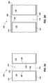
- FIG. 2illustrates a cross-section of another substrate generally at 20 .
- the substrate 20includes a via 22 filled with a metal layer 24 using electroplating as known in the art.
- the metal layer 24was deposited more efficiently near the upper and lower surfaces of the substrate 20 and resulted in the via 22 being substantially closed near the upper and lower surfaces of the substrate 20 while a middle portion of the via 22 was left unfilled.
- the unfilled portion 26 of the via 22is referred to as a keyhole and the presence of the keyhole detracts from the electrical conductivity of the via 22 .
- FIG. 3is a cross-section of a substrate generally at 30 .
- the substrate 30includes a via 32 , being filled using electroless plating as known in the art.
- the substrate 30is placed in a bath for an electroless plating process, also referred to as immersion plating.
- a metal layer 34is formed over a seed layer (not shown) on the sidewall of the via 32 by the continuous deposition of metal until the via 32 is substantially filled with the metal.
- the electroless deposition process of FIG. 3may result in voids or depressions being present in the via 32 .
- the metalsuch as nickel
- the deposition processwould take about one and three-quarter hours to deposit about 35 ⁇ m of metal on the interior of the via 32 (70 ⁇ m/2) as the metal layer 34 grows inwardly toward the center of the via to completely fill the via 32 .
- FIG. 4illustrates a cross-section of a substrate generally at 40 .
- the substrate 40includes a via 42 and a layer of a metal 44 deposited on a bottom 46 of the via 42 and growing towards a top 48 of the via 42 .
- the bottom 46 of the via 42may comprise a suitable metal such as copper (Cu), nickel (Ni) or tungsten (W).
- the approach of the bottom fill processis that by depositing the layer of metal 44 in one direction, upward, and not from the sides of the via 42 (as shown in FIG. 3 ), voids and keyholes are not formed between layers of metal growing towards each other.
- the bottom fill processmay be performed with copper in an attempt to avoid keyhole formation in the via due to migration of the copper.
- the viasmay be as deep as, e.g., 700 microns, and electroless plating deposits metal at the aforementioned relatively slow rate, the process to completely fill the via is unacceptably time consuming.
- Electroplating from the bottom of a viais also known, wherein a conductor serving as a cathode is placed over the bottom of a substrate, covering the bottoms of the vias.
- such an approachseverely limits the stage of wafer processing at which the via may be filled and may impose design limitations on other structures formed or to be formed on the substrate.
- the present inventionin a number of embodiments, overcomes the above difficulties by providing a method for forming a conductive via in a semiconductor component and semiconductor components resulting therefrom.
- the methods of forming conductive vias of the present inventionare faster than known processes since the conductive via is not completely filled with an electroplated or electroless plated metal.
- the conductive vias of the present inventioninclude an annular layer of conductive material that is substantially free of vugs, voids, and keyholes such that the conductivity of the via is not compromised.
- One exemplary embodiment of a method for forming a conductive via in a semiconductor componentincludes providing a substrate having a first surface and an opposing second surface. At least one hole extending from the first surface to the second surface of the substrate is formed through the substrate. A seed layer is applied to the first surface, the second surface and a sidewall defining the at least one hole formed in the substrate. The seed layer overlying the first surface and the opposing second surface of the substrate is removed, leaving the seed layer on the sidewall of the at least one hole. The seed layer on the sidewall is coated with a conductive layer and a conductive or nonconductive filler material is introduced into a remaining space in the at least one hole.
- a second method for fabricating a conductive via through a substratecomprises providing a substrate having a first surface and an opposing second surface. At least one cavity is formed in the first surface of the substrate. A conductive layer is applied over the first surface of the substrate and an exposed area of the substrate that defines the at least one cavity. A filler material is introduced into a remaining space of the at least one cavity. The conductive layer and the filler material introduced into the at least one cavity are exposed on the opposing second surface of the substrate.
- Yet another exemplary embodimentcomprises an intermediate semiconductor component including at least one conductive via precursor structure.
- the intermediate semiconductor componentincludes a substrate having a first surface and an opposing second surface.
- the at least one conductive via precursor structureextends into the first surface of the substrate and terminates in the substrate before reaching the opposing second surface.
- the at least one via precursor structureincludes an annular conductive layer that extends from the first surface and circumscribes a conductive or nonconductive filler material.
- a further exemplary embodiment of the present inventioncomprises a semiconductor component including a substrate having a first surface and an opposing second surface and at least one conductive via extending therebetween.
- the at least one conductive viaincludes an annular conductive layer that extends from the first surface of the substrate to the second surface of the substrate.
- a conductive or nonconductive filler materialis circumscribed by the annular conductive layer and extends from the first surface of the substrate to the opposing, second surface of the substrate.
- the present inventionalso encompasses, in yet another embodiment, a system including a microprocessor and at least one memory device in communication with the microprocessor.
- the at least one memory devicecomprises a substrate having a first surface and an opposing, second surface and at least one conductive via extending therebetween.
- the at least one conductive viaincludes an annular layer of conductive material extending from the first surface of the substrate to the opposing, second surface of the substrate.
- a conductive or nonconductive filler materialis circumscribed by the annular layer of the conductive material and extends from the first surface of the substrate to the opposing, second surface of the substrate.
- the memory devicealso includes at least one bond pad overlying the at least one conductive via.
- FIG. 1is a cross-section of a via in a substrate filled using an electroplating process as known in the art
- FIG. 2illustrates a cross-section of a substrate having a via substantially filled using an electroplating process as known in the art
- FIG. 3depicts a cross-section of a substrate having a via filled using an electroless plating process as known in the art
- FIG. 4is a cross-section of a substrate having a via filled using a bottom fill process as known in the art
- FIGS. 5A through 5Gillustrate acts of an exemplary embodiment of a method for filling vias of the present invention
- FIGS. 6A through 6Hillustrate acts of another exemplary embodiment of a method for filling vias of the present invention
- FIGS. 7A and 7Bdepict acts of another embodiment of a method for forming vias of the present invention.
- FIG. 8depicts a semiconductor component having electrical interconnects formed using the present invention.
- FIG. 9is a schematic diagram of an electronic system incorporating the electrical interconnects fabricated using the methods of the present invention.
- the present inventionincludes methods for manufacturing electrical interconnects, i.e., vias, from one surface of a substrate to the opposite surface of the substrate of a semiconductor component.
- the viasmay electrically connect various electrical structures of the semiconductor component or may be used to electrically connect with other components. It will be apparent to those of ordinary skill in the art that the methods for fabricating vias of the present invention will also be useful in manufacturing interposers and other substrates, such as contactor boards, where electrical interconnects are desired.
- the term “semiconductor component”means and includes electronic components fabricated from semiconductor wafers, other bulk semiconductor substrates, and other substrate materials susceptible to the formation of vias therethrough in accordance with the present invention.
- substratewill refer to any supporting structure in which vias may be formed, including, but not limited to, semiconductor wafers, interposer substrates, contactor boards or other substrate-based structures.
- the inventionincludes methods for fabricating a via through the thickness of a wafer or other substrate, wherein the via includes a conductive liner material and a filler material.
- the filler materialmay be a conductive or nonconductive material.
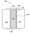
- FIG. 5Athere is shown a cross-section of a semiconductor component generally at 100 .
- the semiconductor component 100includes a substrate 112 having a first surface 114 and an opposing second surface 116 .
- the substrate 112may comprise an unprocessed semiconductor wafer or other substrate, wherein the substrate may have various process layers formed thereon, including one or more semiconductor layers or other structures.
- the substrate 112may further include active portions or other operable portions located thereon, fabricated by etching, deposition or other known techniques.
- the substrate 112may further comprise an interposer substrate for use between a test device and a semiconductor device to be tested (contactor board) or between a memory device and system in a package to provide routing among other substrates.
- the substrate 112comprises a semiconductor material, such as monocrystalline silicon.
- the substrate 112may comprise polycrystalline silicon, germanium, silicon-on-glass, silicon-on-sapphire, a ceramic, a polymer or a glass-filled, epoxy resin material.
- the substrate 112may also comprise any other known substrate material.
- the semiconductor component 100has a via 118 extending from the first surface 114 of the substrate 112 to the second surface 116 .
- the via 118has a substantially cylindrical shape and is defined by an inner surface or sidewall 120 .
- the via 118may have other shapes, such as an hourglass shape or any other known shape for the formation of vias.
- the portions of the substrate 112 that circumscribe an uppermost edge 122 and a lowermost edge 124 of the via 118are illustrated in broken lines. For ease of illustration, the uppermost edge 122 and the lowermost edge 124 of the via 118 will be omitted from subsequent drawings.
- the via 118is formed in the substrate 112 by laser ablation and may have a representative diameter of from about 10 ⁇ m to 2 mils or greater. Typically, the via 118 will have a diameter of about 50 ⁇ m when the semiconductor component 100 is used for stacked chips, interposers, contactor boards or other known electronic components. Since the ratio of the height to width of vias is continually decreasing with the continued miniaturization of integrated circuits, it is contemplated that the via 118 may be formed to have a diameter of about 30 ⁇ m.
- any known method of forming viasthat is appropriate for the type of substrate 112 used to form the semiconductor component 100 may be used to form the via 118 including, without limitation, a dry etch such as a reactive ion etch (RIE), which can remove up to 5 ⁇ m of substrate per minute depending on the type of substrate, photochemical etching, or any other known via formation process.
- RIEreactive ion etch
- the diameter of the via 118 and the thickness of the substrate 112may be any desired dimension depending on the desired use of the semiconductor component 100 .
- the inner surface 120may be cleaned to remove any substrate material affected by the heat produced by the laser ablation process.
- a TMAH (tetramethyl ammonium hydroxide) solutionmay be used to clean the via 118 after formation, which can result in a squared cross-section for the via 118 .
- the cleaned inner surface 120may be passivated by coating the inner surface 120 of the substrate 112 with an insulative layer 126 of dielectric or insulative material appropriate for the type of material of the substrate 112 .
- the insulative layer 126may comprise spin-on-glass, thermal oxide, PARYLENETM polymer, silicon dioxide, silicon nitride, silicon oxynitride, a glass, i.e., borophosphosilicate glass, phosphosilicate glass or borosilicate glass, or any dielectric having a low dielectric constant known in the art.
- the insulative layer 126may be deposited to any desired thickness using any known process, including, without limitation, physical vapor deposition (PVD), CVD, low-pressure chemical vapor deposition (LPCVD), rapid thermal nitridation (RTN), a spin-on-glass (SOG) process, flow coating or any other known process.
- the insulative layer 126may comprise an insulating polymer, such as BT resin, polyimide, benzocyclobutene or polybenzoxazole deposited using an injection or capillary process or a vacuum draw.
- the insulative layer 126may be, for example, of about 1 to 5 ⁇ m in thickness. If the substrate 112 comprises an electrically insulating material, such as ceramic, the insulative layer 126 may be omitted.
- a seed layer 128 of a conductive materialis deposited over the first surface 114 and second surface 116 of the substrate 112 , and the inner surface 120 of the via 118 , wherein the seed layer 128 coats the insulative layer 126 (shown in FIG. 5A ).
- the insulative layer 126 of FIG. 5Ais omitted from FIG. 5B and other subsequent drawings.
- the seed layer 128comprises titanium nitride (TiN) and is deposited by CVD.
- seed layer 128Other materials that may be used as the seed layer 128 include, without limitation, titanium (Ti), silicon nitride (Si 3 N 4 ), a polysilicon, tantalum nitride (TaN), and copper.
- Other deposition processes that may be used to deposit the seed layer 128include PVD, atomic layer deposition (ALD), PECVD, vacuum evaporation, and sputtering. It will be apparent that the selection of the type of material and deposition process utilized to deposit the seed layer 128 will vary depending on the type of material used to form the electrical interconnect through the via 118 .
- a portion of the seed layer 128 covering the first surface 114 and second surface 116 of the substrate 112is removed to expose the first surface 114 and second surface 116 of the substrate 112 as illustrated in FIG. 5C .
- the seed layer 128is removed by an abrasive planarization process such as chemical mechanical planarization (CMP).
- CMPchemical mechanical planarization
- the selective removal of the seed layer 128may be accomplished using any other known process, such as a wet etch or a dry etch, using an etchant appropriate for the type of material making up the seed layer 128 after masking the portion of seed layer 128 within the via 118 .
- the seed layer 128may also be covered with a layer of resist 129 .
- the resist 129is applied to the seed layer 128 before CMP such that the resist 129 prevents particles produced by the CMP process from being deposited in the via 118 .
- the resist 129is removed using known techniques and produces a pristine seed layer 128 surface for the selective deposition of conductive material.
- the first surface 114 and the second surface 116 of the substrate 112may be coated with a nitride layer to prevent the seed layer 128 from being deposited on the first surface 114 and the second surface 116 of the substrate 112 in order to prevent peeling, which may occur depending on the type of conductive material used to coat the surfaces of the substrate 112 and the type of substrate 112 used.
- the via 118may be masked to prevent the nitride layer from being deposited in the via 118 or the nitride layer may be applied on the first surface 114 and second surface 116 of the substrate 112 before the via 118 is formed therein.
- any other material that prevents the seed layer 128 from being deposited on the first surface 114 and the second surface 116 of the substrate 112may be used.
- the seed layer 128is coated with a conductive layer 130 of metal as illustrated in FIG. 5D using an electroless deposition process.
- the conductive layer 130is deposited on the seed layer 128 and not on the exposed first and second surfaces 114 and 116 of the substrate 112 since the seed layer 128 was removed from (or never present on) these surfaces and the electroless deposition process requires the seed layer 128 for deposition of the conductive layer 130 .
- the selective removal of the seed layer 128 from the first surface 114 and the second surface 116 of the substrate 112 and leaving the seed layer 128 in the via 118 or selective deposition of the conductive layer 130 in the via 118obviates the need for a subsequent CMP step to remove excess material.
- the selective deposition of the conductive layer 130reduces the amount of metal used as the conductive layer 130 and, thus, decreases the cost of manufacturing. Further, the selective deposition of the conductive layer 130 in the via 118 helps prevent adhesion issues that may occur when plating a thick conductive layer 130 . Stresses that cause peeling on the conductive layer 130 of the open first surface 114 and the open second surface 116 of the substrate 112 are greater than the peeling stress inside the via 118 .
- the conductive layer 130may comprise any type of metal including, but not limited to, nickel, cobalt, copper, silver, titanium, iridium, gold, tungsten, tantalum, molybdenum, platinum, palladium, nickel-phosphorus (NiP), palladium-phosphorus (Pd—P), cobalt-phosphorus (Co—P), a Co—W—P alloy, other alloys of the foregoing metals and mixtures thereof.
- an annular conductive pathis created through the via 118 .
- the electroless plating processforms a substantially conformal coating in the via 118 that is substantially free of any voids or keyholes.
- the conductive layer 130 formed from the electroless plating processwill typically have a uniform thickness and a low porosity, will provide corrosion protection and will be relatively hard.
- the electroless plating processis accomplished by placing the substrate 112 into a bath containing an aqueous solution of the metal to be deposited in ionic form.
- the aqueous solutionalso includes a chemical reducing agent such that the metal may be deposited without the use of electrical energy.
- the driving force for the reduction of the metal ions and subsequent deposition in the electroless plating processis driven by the chemical reducing agent.
- the reduction reactionis essentially constant at all points on the seed layer 128 so long as the aqueous solution is sufficiently agitated (for example, by ultrasound) to ensure that a uniform concentration of metal ions and reducing agents are distributed in the aqueous solution.
- the conductive layer 130is lined with silver or gold using an immersion process, such as an immersion plating process. If the conductive layer 130 includes nickel or cobalt, the silver or gold lining will replace the nickel or cobalt, since silver and gold are more noble than nickel and cobalt. The silver or gold lining will increase conductivity and aid in wetting the solder to help ensure a void-less fill of solder and continuous contact of solder with the sidewalls of the via 118 .
- the deposition of the conductive layer 130may result in a small portion 132 of the conductive layer 130 extending beyond the plane of the first surface 114 or the second surface 116 of the substrate 112 .
- the small portion 132may be removed, if desired, using CMP or another known removal process, such that the conductive layer 130 is substantially even with the plane of the first surface 114 and the second surface 116 of the substrate 112 as illustrated in FIG. 5E .
- the via 118has an opening 134 extending from the first surface 114 to the second surface 116 wherein the opening 134 is circumscribed by the conductive layer 130 .
- the electroless plating process used to form the conductive layer 130may incidentally result in minor depressions or voids in the conductive layer 130
- the thickness of the conductive layer 130 required to accommodate the desired conductivityshould be of a dimension such that any voids or depressions should not affect the conductivity.
- the opening 134 of the via 118is filled with a filler material 136 as illustrated in FIG. 5F .
- the filler material 136may be a conductive or a nonconductive material depending on the desired conductivity of the filled via 118 and intended use of the semiconductor component 100 . For instance, since the conductivity of the filled via 118 is at least minimally determined by the material and thickness of the conductive layer 130 , a nonconductive material may be used to fill the opening 134 of the via 118 if conductive layer 130 provides an adequate conductive path.
- Non-limiting, representative examples of substances that may be used for the filler material 136include silicon-containing fillers such as spin-on-glass (SOG) applied using a spin coat process for a nonconductive filler material 136 or polysilicon applied using a diffusion process and doped for a conductive filler material 136 .
- SOGspin-on-glass
- solder paste applied with a squeegee and subsequently reflowedmay also be used as a conductive filler material 136 .
- the solder pastemay include eutectic solder, Cu—Sn—Ag, Sn—Ag, other known solder materials, or combinations thereof.
- Other filler materials 136 that may be usedinclude, without limitation, a solder alloy screen printed in the opening 134 , conductive and nonconductive polymers, metal-filled silicon, carbon-filled ink, isotropically or anisotropically conductive adhesives and conductor-filled epoxies, such as silver-filled epoxy paste.
- any protruding filler material 136may be removed using CMP or other known smoothing processes such that bond pads 138 may be formed over one or both ends of the via 118 as known in the art and shown in FIG. 5G .
- the filler material 136provides physical support to the bond pads 138 overlying the via 118 .
- a blind viamay be used to form the conductive via of the present invention.
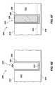
- a cross-section of a semiconductor componentis shown generally at 200 in FIG. 6A .
- the semiconductor component 200comprises a substrate 212 having a first surface 214 and an opposing second surface 216 .
- the substrate 212may comprise an unprocessed semiconductor wafer or other substrate material used in fabrication processes as previously described herein with reference to the substrate 112 of FIG. 5A .
- the semiconductor component 200includes a blind via 218 that partially penetrates the substrate 212 and substantially extends through the substrate 212 from the first surface 214 and wherein a bottom 213 of the blind via 218 terminates short of the second surface 216 of the substrate 212 .
- the blind via 218may be formed in the substrate 212 using a laser ablation process or in any other manner as the via 118 was formed in the substrate 112 as described herein with reference to FIG. 5A .
- the blind via 218is circumscribed by an inner surface or sidewall 220 of the substrate 212 .
- the portion of the substrate 212 that circumscribes an uppermost edge 222 of the blind via 218is illustrated in broken lines, which, for ease of illustration, is omitted from subsequent drawings.
- the blind via 218may also comprise an opening in the substrate 212 that extends through the substrate 212 (substantially similar to the via 118 of FIG. 5A ) that is sealably covered or capped with a cover layer 225 and illustrated with phantom lines 224 .
- the cover layer 225substantially seals the blind via 218 such that, in essence, the covered via is filled in substantially the same manner as the blind via 218 .
- a seed layer(not shown) may thus also be deposited on the cover layer 225 forming the bottom 213 of blind via 218 .
- the cover layer 225may comprise a metal layer attached to the substrate 212 before the blind via 218 is formed in the substrate 212 . Laser ablation may then be used to partially form the blind via 218 that is then completed using a dry etch, which will stop on the metal of cover layer 225 .
- the blind via 218may be insulated with a passivation layer (not shown) if required.
- the wafer chuck 217may be used to support the semiconductor component 200 during the fabrication process and the illustration of the wafer chuck 217 will be omitted from subsequent drawings.
- the inner surface 220 of the blind via 218may be cleaned to remove any debris, residual material or substrate material adversely affected by the formation of the blind via 218 .
- the cleaned inner surface 220may be passivated by coating the inner surface 220 of the substrate 212 with a layer of dielectric or insulative material appropriate for the type of substrate 212 .
- the passivation layeris not depicted in FIG. 6A , but it will be apparent to those of ordinary skill in the art that the passivation layer of the blind via 218 may be substantially similar to the insulative layer 126 as described with reference to FIG. 5A . Further, depending on the material of substrate 212 , the passivation layer may be omitted.
- the semiconductor component 200is shown with a seed layer 228 of conductive metal formed on the first surface 214 of the substrate 212 and the inner surface 220 of the blind via 218 .
- the seed layer 228is TiN and is deposited by CVD.
- the seed layer 228may comprise any other material as described herein with reference to the seed layer 128 of FIG. 5B .
- the portion of the seed layer 228 covering the first surface 214 of the substrate 212is removed by CMP to expose the first surface 214 of the substrate 212 as illustrated in FIG. 6C . It will be apparent that the seed layer 228 may be removed using any known process as previously described herein.
- a conductive layer 230is deposited overlying the seed layer 228 , as illustrated in FIG. 6D , using an electroless deposition process as previously described herein. The conductive layer 230 will not adhere to the first surface 214 of the substrate 212 since no seed layer 228 is present on the first surface 214 of the substrate 212 .
- the conductive layer 230may comprise any conductive metal as described herein with reference to the conductive layer 130 of FIG. 5D wherein the type and thickness of the metal utilized in the conductive layer 230 will vary depending on the desired conductivity and ultimate use of the semiconductor component 200 .
- a layer of resist 229is placed over the seed layer 228 before CMP.
- the presence of the resist 229prevents particles produced by the CMP process from contaminating the blind via 218 .
- the resist 229is removed using known techniques and results in a pristine surface for the subsequent deposition of the conductive layer 230 .
- a portion 232 of the conductive layer 230may extend beyond a plane of the first surface 214 of the substrate 212 . If this occurs, the portion 232 of the conductive layer 230 extending beyond the plane of the first surface 214 may be removed as previously described herein with reference to FIG. 5E and result in the semiconductor component 200 of FIG. 6E . In another exemplary embodiment, the portion 232 of the conductive layer 230 extending above the plane of the first surface 214 of the substrate 212 may be left in place and used, at least partially, to form at least a portion of a bond pad (shown in FIG. 6H ) subsequently constructed on the first surface 214 of the substrate 212 .
- the conductive layer 230may be lined with silver or gold using an immersion plating process in another exemplary embodiment. If the conductive layer 230 includes nickel or cobalt, the nickel or cobalt will be replaced with the silver or gold, since silver and gold are more noble. The inclusion of the silver or gold lining in the conductive layer 230 will also increase conductivity and aid in wetting the solder.
- the blind via 218includes an opening 234 substantially surrounded by the conductive layer 230 that extends from the first surface 214 of the substrate 212 and substantially through the substrate 212 to and over the bottom 213 of the blind via 218 .
- the opening 234 of the blind via 218is filled with a filler material 236 as illustrated with cross-hatching in FIG. 6F .
- the filler material 236may comprise a conductive or a nonconductive material depending on the desired conductivity of the filled blind via 218 as previously described herein with reference to FIG. 5F .
- the second surface 216 of the substrate 212is removed from the semiconductor component 200 using an abrasive planarization process such as CMP or any other known suitable removal process. Material of the substrate 212 is removed to a depth illustrated by broken line 240 in FIG. 6F such that the blind via 218 is exposed on the second surface 216 of the substrate 212 as illustrated in FIG. 6G . Bond pads 238 are formed over opposing ends of the blind via 218 as is known in the art and as illustrated in FIG. 6H . In a variation of this exemplary embodiment, if blind via 218 extended through the substrate 212 to cover layer 225 , as described with reference to FIG. 6A , the cover layer 225 may be removed to expose the blind via 218 lined with conductive layer 230 and filled with filler material 236 .
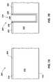
- FIGS. 7A and 7BAnother exemplary embodiment of acts in the methods of the present invention is depicted in FIGS. 7A and 7B .
- a semiconductor componentis shown generally at 200 ′.
- the semiconductor component 200 ′includes a substrate 212 having a first surface 214 and an opposing, second surface 216 .
- a barrier layer 203is formed on the first surface 214 of the substrate 212 .
- the barrier layer 203comprises a material that prevents a seed layer 228 from being deposited thereon.
- the barrier layer 203may comprise an oxide- or a nitride-containing material such as silicon dioxide or silicon nitride.
- a blind via 218is formed through the barrier layer 203 and in the substrate 212 .
- the seed layer 228 and a conductive layer 230are formed in the blind via 218 , whereafter a remaining opening 234 of the blind via 218 is filled with the filler material as previously discussed herein.
- the fabrication of the conductive blind via 218may be completed as previously described.
- the semiconductor component 300includes a substrate 312 with a conductive via 318 .
- the conductive via 318includes a filler material 336 and an annular conductive liner 330 that forms an electrical connection between bonds pads 338 located on opposing surfaces of the semiconductor component 300 .
- the semiconductor component 300may include circuit traces 340 or other interconnects and contact structures to electrically connect the via 318 to contact pads 342 or other conductive structures.
- the circuit traces 340 or other conductive structuresmay also be used to connect circuitry of semiconductor component 300 to other circuits such as integrated circuitry formed on an opposing side of substrate 312 , to circuits of another semiconductor component disposed over or under semiconductor component 300 in a stack, to an interposer, to a contactor board, or to a carrier substrate such as a motherboard or module board bearing other semiconductor components such as a microprocessor.
- the blanket material layer from which bond pads 338 are formedmay also be patterned to define the circuit traces 340 leading from the via 318 to the contact pads 342 .
- the conductive via 318thus may be used to electrically connect contact pads 342 on a first surface 314 of the substrate 312 to contact pads 342 on a second surface 316 of the substrate 312 .
- the substrate 312 of the semiconductor component 300may be designed and fabricated as an interposer for connecting various semiconductor components, as a semiconductor test substrate (contactor board) or as a carrier substrate forming higher-level packaging to which semiconductor chips may be connected.
- the bond pads 338 or contact pads 342 of the semiconductor component 300may be arranged in a pattern that corresponds to that of terminal pads on a test or carrier substrate.
- bond pads 338 or contact pads 342may be arranged in a pattern on one side of substrate 312 to correspond to terminal pads of a test or carrier substrate and on the other side to correspond to bond pad or other I/O locations on a semiconductor device to be contacted.
- the system 400comprises at least one memory device 402 , such as a static random access memory (SRAM), dynamic random access memory (DRAM), or other known memory device, wherein the at least one memory device 402 includes at least one conductive via fabricated using the methods of the present invention.
- the memory device 402is operatively coupled to a microprocessor 404 that may be programmed to carry out particular functions as is known in the art.
Landscapes
- Engineering & Computer Science (AREA)
- Microelectronics & Electronic Packaging (AREA)
- Physics & Mathematics (AREA)
- Condensed Matter Physics & Semiconductors (AREA)
- General Physics & Mathematics (AREA)
- Computer Hardware Design (AREA)
- Power Engineering (AREA)
- Manufacturing & Machinery (AREA)
- Internal Circuitry In Semiconductor Integrated Circuit Devices (AREA)
Abstract
Description
Claims (25)
Priority Applications (2)
| Application Number | Priority Date | Filing Date | Title |
|---|---|---|---|
| US12/648,864US8148263B2 (en) | 2003-09-23 | 2009-12-29 | Methods for forming conductive vias in semiconductor device components |
| US13/404,631US9287207B2 (en) | 2003-09-23 | 2012-02-24 | Methods for forming conductive vias in semiconductor device components |
Applications Claiming Priority (3)
| Application Number | Priority Date | Filing Date | Title |
|---|---|---|---|
| US10/668,914US7345350B2 (en) | 2003-09-23 | 2003-09-23 | Process and integration scheme for fabricating conductive components, through-vias and semiconductor components including conductive through-wafer vias |
| US11/717,437US7666788B2 (en) | 2003-09-23 | 2007-03-12 | Methods for forming conductive vias in semiconductor device components |
| US12/648,864US8148263B2 (en) | 2003-09-23 | 2009-12-29 | Methods for forming conductive vias in semiconductor device components |
Related Parent Applications (1)
| Application Number | Title | Priority Date | Filing Date |
|---|---|---|---|
| US11/717,437ContinuationUS7666788B2 (en) | 2003-09-23 | 2007-03-12 | Methods for forming conductive vias in semiconductor device components |
Related Child Applications (1)
| Application Number | Title | Priority Date | Filing Date |
|---|---|---|---|
| US13/404,631ContinuationUS9287207B2 (en) | 2003-09-23 | 2012-02-24 | Methods for forming conductive vias in semiconductor device components |
Publications (2)
| Publication Number | Publication Date |
|---|---|
| US20100133661A1 US20100133661A1 (en) | 2010-06-03 |
| US8148263B2true US8148263B2 (en) | 2012-04-03 |
Family
ID=34313613
Family Applications (5)
| Application Number | Title | Priority Date | Filing Date |
|---|---|---|---|
| US10/668,914Expired - LifetimeUS7345350B2 (en) | 2003-09-23 | 2003-09-23 | Process and integration scheme for fabricating conductive components, through-vias and semiconductor components including conductive through-wafer vias |
| US11/717,294Expired - LifetimeUS7608904B2 (en) | 2003-09-23 | 2007-03-12 | Semiconductor device components with conductive vias and systems including the components |
| US11/717,437Expired - LifetimeUS7666788B2 (en) | 2003-09-23 | 2007-03-12 | Methods for forming conductive vias in semiconductor device components |
| US12/648,864Expired - LifetimeUS8148263B2 (en) | 2003-09-23 | 2009-12-29 | Methods for forming conductive vias in semiconductor device components |
| US13/404,631Expired - LifetimeUS9287207B2 (en) | 2003-09-23 | 2012-02-24 | Methods for forming conductive vias in semiconductor device components |
Family Applications Before (3)
| Application Number | Title | Priority Date | Filing Date |
|---|---|---|---|
| US10/668,914Expired - LifetimeUS7345350B2 (en) | 2003-09-23 | 2003-09-23 | Process and integration scheme for fabricating conductive components, through-vias and semiconductor components including conductive through-wafer vias |
| US11/717,294Expired - LifetimeUS7608904B2 (en) | 2003-09-23 | 2007-03-12 | Semiconductor device components with conductive vias and systems including the components |
| US11/717,437Expired - LifetimeUS7666788B2 (en) | 2003-09-23 | 2007-03-12 | Methods for forming conductive vias in semiconductor device components |
Family Applications After (1)
| Application Number | Title | Priority Date | Filing Date |
|---|---|---|---|
| US13/404,631Expired - LifetimeUS9287207B2 (en) | 2003-09-23 | 2012-02-24 | Methods for forming conductive vias in semiconductor device components |
Country Status (7)
| Country | Link |
|---|---|
| US (5) | US7345350B2 (en) |
| EP (2) | EP2393109B1 (en) |
| JP (2) | JP5093563B2 (en) |
| KR (1) | KR20070006667A (en) |
| CN (1) | CN100483653C (en) |
| TW (1) | TWI293793B (en) |
| WO (1) | WO2005031811A2 (en) |
Cited By (4)
| Publication number | Priority date | Publication date | Assignee | Title |
|---|---|---|---|---|
| US20120038049A1 (en)* | 2008-12-16 | 2012-02-16 | Achim Trautmann | Component having a via, and a method for manufacturing such a component |
| US9596768B2 (en) | 2014-03-04 | 2017-03-14 | Qualcomm Incorporated | Substrate with conductive vias |
| US10790426B2 (en)* | 2016-04-01 | 2020-09-29 | Nichia Corporation | Method of manufacturing light emitting element mounting base member, method of manufacturing light emitting device using the light emitting element mounting base member, light emitting element mounting base member, and light emitting device using the light emitting element mounting base member |
| US12087623B1 (en)* | 2024-01-25 | 2024-09-10 | Yield Engineering Systems, Inc. | Dielectric liners on through glass vias |
Families Citing this family (291)
| Publication number | Priority date | Publication date | Assignee | Title |
|---|---|---|---|---|
| US7345350B2 (en) | 2003-09-23 | 2008-03-18 | Micron Technology, Inc. | Process and integration scheme for fabricating conductive components, through-vias and semiconductor components including conductive through-wafer vias |
| US7364985B2 (en)* | 2003-09-29 | 2008-04-29 | Micron Technology, Inc. | Method for creating electrical pathways for semiconductor device structures using laser machining processes |
| US7091124B2 (en)* | 2003-11-13 | 2006-08-15 | Micron Technology, Inc. | Methods for forming vias in microelectronic devices, and methods for packaging microelectronic devices |
| US8084866B2 (en) | 2003-12-10 | 2011-12-27 | Micron Technology, Inc. | Microelectronic devices and methods for filling vias in microelectronic devices |
| DE10355600B4 (en)* | 2003-11-28 | 2021-06-24 | OSRAM Opto Semiconductors Gesellschaft mit beschränkter Haftung | Semiconductor chip and method for manufacturing semiconductor chips |
| US6943106B1 (en)* | 2004-02-20 | 2005-09-13 | Micron Technology, Inc. | Methods of fabricating interconnects for semiconductor components including plating solder-wetting material and solder filling |
| TWI244143B (en)* | 2004-03-02 | 2005-11-21 | Via Tech Inc | Process of plating through hole |
| JP2005303258A (en)* | 2004-03-16 | 2005-10-27 | Fujikura Ltd | Device and manufacturing method thereof |
| US20050247894A1 (en) | 2004-05-05 | 2005-11-10 | Watkins Charles M | Systems and methods for forming apertures in microfeature workpieces |
| US7232754B2 (en)* | 2004-06-29 | 2007-06-19 | Micron Technology, Inc. | Microelectronic devices and methods for forming interconnects in microelectronic devices |
| US7425499B2 (en)* | 2004-08-24 | 2008-09-16 | Micron Technology, Inc. | Methods for forming interconnects in vias and microelectronic workpieces including such interconnects |
| SG120200A1 (en) | 2004-08-27 | 2006-03-28 | Micron Technology Inc | Slanted vias for electrical circuits on circuit boards and other substrates |
| US7300857B2 (en) | 2004-09-02 | 2007-11-27 | Micron Technology, Inc. | Through-wafer interconnects for photoimager and memory wafers |
| US7271482B2 (en) | 2004-12-30 | 2007-09-18 | Micron Technology, Inc. | Methods for forming interconnects in microelectronic workpieces and microelectronic workpieces formed using such methods |
| US20060252262A1 (en)* | 2005-05-03 | 2006-11-09 | Rockwell Scientific Licensing, Llc | Semiconductor structures having via structures between planar frontside and backside surfaces and methods of fabricating the same |
| US20090117336A1 (en)* | 2005-06-01 | 2009-05-07 | Matsushita Electric Industrial Co., Ltd | Circuit board, method for manufacturing such circuit board, and electronic component using such circuit board |
| JP4581864B2 (en)* | 2005-06-21 | 2010-11-17 | パナソニック電工株式会社 | Method for forming through wiring on semiconductor substrate |
| US7795134B2 (en) | 2005-06-28 | 2010-09-14 | Micron Technology, Inc. | Conductive interconnect structures and formation methods using supercritical fluids |
| JP5096669B2 (en) | 2005-07-06 | 2012-12-12 | ルネサスエレクトロニクス株式会社 | Manufacturing method of semiconductor integrated circuit device |
| US20070045844A1 (en)* | 2005-08-24 | 2007-03-01 | Andry Paul S | Alpha particle shields in chip packaging |
| US8308053B2 (en)* | 2005-08-31 | 2012-11-13 | Micron Technology, Inc. | Microfeature workpieces having alloyed conductive structures, and associated methods |
| US7262134B2 (en) | 2005-09-01 | 2007-08-28 | Micron Technology, Inc. | Microfeature workpieces and methods for forming interconnects in microfeature workpieces |
| US7622377B2 (en) | 2005-09-01 | 2009-11-24 | Micron Technology, Inc. | Microfeature workpiece substrates having through-substrate vias, and associated methods of formation |
| US7772115B2 (en)* | 2005-09-01 | 2010-08-10 | Micron Technology, Inc. | Methods for forming through-wafer interconnects, intermediate structures so formed, and devices and systems having at least one solder dam structure |
| US7863187B2 (en) | 2005-09-01 | 2011-01-04 | Micron Technology, Inc. | Microfeature workpieces and methods for forming interconnects in microfeature workpieces |
| WO2007089206A1 (en)* | 2006-02-01 | 2007-08-09 | Silex Microsystems Ab | Vias and method of making |
| US7892972B2 (en)* | 2006-02-03 | 2011-02-22 | Micron Technology, Inc. | Methods for fabricating and filling conductive vias and conductive vias so formed |
| KR100783467B1 (en)* | 2006-02-24 | 2007-12-07 | 삼성전기주식회사 | Printed Circuit Board with Internal Through Hole and Manufacturing Method Thereof |
| US7404251B2 (en)* | 2006-04-18 | 2008-07-29 | International Business Machines Corporation | Manufacture of printed circuit boards with stubless plated through-holes |
| US7749899B2 (en) | 2006-06-01 | 2010-07-06 | Micron Technology, Inc. | Microelectronic workpieces and methods and systems for forming interconnects in microelectronic workpieces |
| US7629249B2 (en) | 2006-08-28 | 2009-12-08 | Micron Technology, Inc. | Microfeature workpieces having conductive interconnect structures formed by chemically reactive processes, and associated systems and methods |
| US7560371B2 (en)* | 2006-08-29 | 2009-07-14 | Micron Technology, Inc. | Methods for selectively filling apertures in a substrate to form conductive vias with a liquid using a vacuum |
| US7902643B2 (en) | 2006-08-31 | 2011-03-08 | Micron Technology, Inc. | Microfeature workpieces having interconnects and conductive backplanes, and associated systems and methods |
| US20080261392A1 (en)* | 2007-04-23 | 2008-10-23 | John Trezza | Conductive via formation |
| US8232183B2 (en)* | 2007-05-04 | 2012-07-31 | Taiwan Semiconductor Manufacturing Company, Ltd. | Process and apparatus for wafer-level flip-chip assembly |
| US7886437B2 (en)* | 2007-05-25 | 2011-02-15 | Electro Scientific Industries, Inc. | Process for forming an isolated electrically conductive contact through a metal package |
| US8003517B2 (en)* | 2007-05-29 | 2011-08-23 | Freescale Semiconductor, Inc. | Method for forming interconnects for 3-D applications |
| US7982137B2 (en)* | 2007-06-27 | 2011-07-19 | Hamilton Sundstrand Corporation | Circuit board with an attached die and intermediate interposer |
| SG150410A1 (en) | 2007-08-31 | 2009-03-30 | Micron Technology Inc | Partitioned through-layer via and associated systems and methods |
| TW200915505A (en)* | 2007-09-29 | 2009-04-01 | Kinik Co | Packaging carrier with high heat-dissipation and method for manufacturing the same |
| US8293587B2 (en)* | 2007-10-11 | 2012-10-23 | International Business Machines Corporation | Multilayer pillar for reduced stress interconnect and method of making same |
| TWI396269B (en)* | 2007-10-17 | 2013-05-11 | Unimicron Technology Corp | Method for fabricating printed circuit board |
| US8492263B2 (en)* | 2007-11-16 | 2013-07-23 | Taiwan Semiconductor Manufacturing Company, Ltd. | Protected solder ball joints in wafer level chip-scale packaging |
| US8440917B2 (en)* | 2007-11-19 | 2013-05-14 | International Business Machines Corporation | Method and apparatus to reduce impedance discontinuity in packages |
| US7884015B2 (en) | 2007-12-06 | 2011-02-08 | Micron Technology, Inc. | Methods for forming interconnects in microelectronic workpieces and microelectronic workpieces formed using such methods |
| US8084854B2 (en) | 2007-12-28 | 2011-12-27 | Micron Technology, Inc. | Pass-through 3D interconnect for microelectronic dies and associated systems and methods |
| KR101070798B1 (en)* | 2008-01-15 | 2011-10-06 | 삼성전기주식회사 | PCB and manufacturing method thereof |
| KR20100126714A (en)* | 2008-01-30 | 2010-12-02 | 이노벤트 테크놀로지스, 엘엘씨 | Method and apparatus for manufacturing via disk |
| US7898063B2 (en)* | 2008-02-16 | 2011-03-01 | International Business Machines Corporation | Through substrate annular via including plug filler |
| US8106511B2 (en)* | 2008-02-28 | 2012-01-31 | Qimonda Ag | Reduced-stress through-chip feature and method of making the same |
| US9136259B2 (en)* | 2008-04-11 | 2015-09-15 | Micron Technology, Inc. | Method of creating alignment/centering guides for small diameter, high density through-wafer via die stacking |
| KR101052870B1 (en)* | 2008-04-21 | 2011-07-29 | 주식회사 하이닉스반도체 | A laminated semiconductor package having a through electrode, a circuit board having the same, a semiconductor package having the same, and a semiconductor package |
| US8253230B2 (en) | 2008-05-15 | 2012-08-28 | Micron Technology, Inc. | Disabling electrical connections using pass-through 3D interconnects and associated systems and methods |
| US8334170B2 (en) | 2008-06-27 | 2012-12-18 | Taiwan Semiconductor Manufacturing Company, Ltd. | Method for stacking devices |
| US7851346B2 (en)* | 2008-07-21 | 2010-12-14 | Taiwan Semiconductor Manufacturing Company, Ltd. | Bonding metallurgy for three-dimensional interconnect |
| US8035198B2 (en)* | 2008-08-08 | 2011-10-11 | International Business Machines Corporation | Through wafer via and method of making same |
| US8932906B2 (en) | 2008-08-19 | 2015-01-13 | Taiwan Semiconductor Manufacturing Company, Ltd. | Through silicon via bonding structure |
| DE102008044985B4 (en)* | 2008-08-29 | 2010-08-12 | Advanced Micro Devices, Inc., Sunnyvale | A method of making a semiconductor device having a carbonaceous conductive material for via contacts |
| WO2010022973A1 (en)* | 2008-08-29 | 2010-03-04 | Advanced Micro Devices Inc. | A semiconductor device comprising a carbon based material for through hole vias |
| US9524945B2 (en) | 2010-05-18 | 2016-12-20 | Taiwan Semiconductor Manufacturing Company, Ltd. | Cu pillar bump with L-shaped non-metal sidewall protection structure |
| US7943421B2 (en)* | 2008-12-05 | 2011-05-17 | Taiwan Semiconductor Manufacturing Company, Ltd. | Component stacking using pre-formed adhesive films |
| US7867891B2 (en)* | 2008-12-10 | 2011-01-11 | Intel Corporation | Dual metal interconnects for improved gap-fill, reliability, and reduced capacitance |
| TWI420643B (en)* | 2008-12-16 | 2013-12-21 | Powertech Technology Inc | Chip having tsv's, its forming method and a chip stack utilizing the chip |
| US9117828B2 (en)* | 2009-03-27 | 2015-08-25 | Taiwan Semiconductor Manufacturing Company, Ltd. | Method of handling a thin wafer |
| US8362368B2 (en)* | 2009-04-27 | 2013-01-29 | Ultrasource, Inc. | Method and apparatus for an improved filled via |
| WO2010147939A1 (en) | 2009-06-17 | 2010-12-23 | Hsio Technologies, Llc | Semiconductor socket |
| US9276336B2 (en) | 2009-05-28 | 2016-03-01 | Hsio Technologies, Llc | Metalized pad to electrical contact interface |
| US9536815B2 (en) | 2009-05-28 | 2017-01-03 | Hsio Technologies, Llc | Semiconductor socket with direct selective metalization |
| WO2011153298A1 (en) | 2010-06-03 | 2011-12-08 | Hsio Technologies, Llc | Electrical connector insulator housing |
| US8955215B2 (en) | 2009-05-28 | 2015-02-17 | Hsio Technologies, Llc | High performance surface mount electrical interconnect |
| WO2012074963A1 (en) | 2010-12-01 | 2012-06-07 | Hsio Technologies, Llc | High performance surface mount electrical interconnect |
| US9196980B2 (en) | 2009-06-02 | 2015-11-24 | Hsio Technologies, Llc | High performance surface mount electrical interconnect with external biased normal force loading |
| US9414500B2 (en) | 2009-06-02 | 2016-08-09 | Hsio Technologies, Llc | Compliant printed flexible circuit |
| WO2010141298A1 (en) | 2009-06-02 | 2010-12-09 | Hsio Technologies, Llc | Composite polymer-metal electrical contacts |
| US8912812B2 (en) | 2009-06-02 | 2014-12-16 | Hsio Technologies, Llc | Compliant printed circuit wafer probe diagnostic tool |
| US8525346B2 (en) | 2009-06-02 | 2013-09-03 | Hsio Technologies, Llc | Compliant conductive nano-particle electrical interconnect |
| US9184145B2 (en) | 2009-06-02 | 2015-11-10 | Hsio Technologies, Llc | Semiconductor device package adapter |
| WO2010141296A1 (en) | 2009-06-02 | 2010-12-09 | Hsio Technologies, Llc | Compliant printed circuit semiconductor package |
| US9231328B2 (en) | 2009-06-02 | 2016-01-05 | Hsio Technologies, Llc | Resilient conductive electrical interconnect |
| US8955216B2 (en) | 2009-06-02 | 2015-02-17 | Hsio Technologies, Llc | Method of making a compliant printed circuit peripheral lead semiconductor package |
| WO2010141318A1 (en) | 2009-06-02 | 2010-12-09 | Hsio Technologies, Llc | Compliant printed circuit peripheral lead semiconductor test socket |
| US9603249B2 (en) | 2009-06-02 | 2017-03-21 | Hsio Technologies, Llc | Direct metalization of electrical circuit structures |
| WO2010141313A1 (en) | 2009-06-02 | 2010-12-09 | Hsio Technologies, Llc | Compliant printed circuit socket diagnostic tool |
| WO2011002709A1 (en) | 2009-06-29 | 2011-01-06 | Hsio Technologies, Llc | Compliant printed circuit semiconductor tester interface |
| US8610265B2 (en) | 2009-06-02 | 2013-12-17 | Hsio Technologies, Llc | Compliant core peripheral lead semiconductor test socket |
| US8988093B2 (en) | 2009-06-02 | 2015-03-24 | Hsio Technologies, Llc | Bumped semiconductor wafer or die level electrical interconnect |
| US9699906B2 (en) | 2009-06-02 | 2017-07-04 | Hsio Technologies, Llc | Hybrid printed circuit assembly with low density main core and embedded high density circuit regions |
| US9930775B2 (en) | 2009-06-02 | 2018-03-27 | Hsio Technologies, Llc | Copper pillar full metal via electrical circuit structure |
| US9613841B2 (en) | 2009-06-02 | 2017-04-04 | Hsio Technologies, Llc | Area array semiconductor device package interconnect structure with optional package-to-package or flexible circuit to package connection |
| US9318862B2 (en) | 2009-06-02 | 2016-04-19 | Hsio Technologies, Llc | Method of making an electronic interconnect |
| US9054097B2 (en) | 2009-06-02 | 2015-06-09 | Hsio Technologies, Llc | Compliant printed circuit area array semiconductor device package |
| US9136196B2 (en) | 2009-06-02 | 2015-09-15 | Hsio Technologies, Llc | Compliant printed circuit wafer level semiconductor package |
| WO2010147934A1 (en) | 2009-06-16 | 2010-12-23 | Hsio Technologies, Llc | Semiconductor die terminal |
| WO2010141264A1 (en) | 2009-06-03 | 2010-12-09 | Hsio Technologies, Llc | Compliant wafer level probe assembly |
| US9320133B2 (en) | 2009-06-02 | 2016-04-19 | Hsio Technologies, Llc | Electrical interconnect IC device socket |
| US9232654B2 (en) | 2009-06-02 | 2016-01-05 | Hsio Technologies, Llc | High performance electrical circuit structure |
| US9276339B2 (en) | 2009-06-02 | 2016-03-01 | Hsio Technologies, Llc | Electrical interconnect IC device socket |
| US8987886B2 (en) | 2009-06-02 | 2015-03-24 | Hsio Technologies, Llc | Copper pillar full metal via electrical circuit structure |
| WO2010147782A1 (en) | 2009-06-16 | 2010-12-23 | Hsio Technologies, Llc | Simulated wirebond semiconductor package |
| US8984748B2 (en) | 2009-06-29 | 2015-03-24 | Hsio Technologies, Llc | Singulated semiconductor device separable electrical interconnect |
| US8841766B2 (en)* | 2009-07-30 | 2014-09-23 | Taiwan Semiconductor Manufacturing Company, Ltd. | Cu pillar bump with non-metal sidewall protection structure |
| US8377816B2 (en) | 2009-07-30 | 2013-02-19 | Taiwan Semiconductor Manufacturing Company, Ltd. | Method of forming electrical connections |
| US8428762B2 (en)* | 2009-08-28 | 2013-04-23 | Kla-Tencor Corporation | Spin coating modeling |
| US8324738B2 (en) | 2009-09-01 | 2012-12-04 | Taiwan Semiconductor Manufacturing Company, Ltd. | Self-aligned protection layer for copper post structure |
| US8803332B2 (en)* | 2009-09-11 | 2014-08-12 | Taiwan Semiconductor Manufacturing Company, Ltd. | Delamination resistance of stacked dies in die saw |
| US8173536B2 (en)* | 2009-11-02 | 2012-05-08 | Stats Chippac, Ltd. | Semiconductor device and method of forming column interconnect structure to reduce wafer stress |
| US8659155B2 (en) | 2009-11-05 | 2014-02-25 | Taiwan Semiconductor Manufacturing Company, Ltd. | Mechanisms for forming copper pillar bumps |
| KR20110050957A (en) | 2009-11-09 | 2011-05-17 | 삼성전자주식회사 | Through-via contact of semiconductor device and forming method |
| TWI370532B (en)* | 2009-11-12 | 2012-08-11 | Ind Tech Res Inst | Chip package structure and method for fabricating the same |
| US20110115069A1 (en)* | 2009-11-13 | 2011-05-19 | Serene Seoh Hian Teh | Electronic device including a packaging substrate and an electrical conductor within a via and a process of forming the same |
| JP5218497B2 (en)* | 2009-12-04 | 2013-06-26 | 株式会社デンソー | Semiconductor device and manufacturing method thereof |
| JP5600427B2 (en)* | 2009-12-25 | 2014-10-01 | 株式会社フジクラ | Material substrate for through wiring board |
| US8569894B2 (en) | 2010-01-13 | 2013-10-29 | Advanced Semiconductor Engineering, Inc. | Semiconductor package with single sided substrate design and manufacturing methods thereof |
| US8299616B2 (en)* | 2010-01-29 | 2012-10-30 | Taiwan Semiconductor Manufacturing Company, Ltd. | T-shaped post for semiconductor devices |
| US10297550B2 (en) | 2010-02-05 | 2019-05-21 | Taiwan Semiconductor Manufacturing Company, Ltd. | 3D IC architecture with interposer and interconnect structure for bonding dies |
| US8610270B2 (en)* | 2010-02-09 | 2013-12-17 | Taiwan Semiconductor Manufacturing Company, Ltd. | Semiconductor device and semiconductor assembly with lead-free solder |
| US8318596B2 (en) | 2010-02-11 | 2012-11-27 | Taiwan Semiconductor Manufacturing Company, Ltd. | Pillar structure having a non-planar surface for semiconductor devices |
| US8803319B2 (en) | 2010-02-11 | 2014-08-12 | Taiwan Semiconductor Manufacturing Company, Ltd. | Pillar structure having a non-planar surface for semiconductor devices |
| JP5609144B2 (en)* | 2010-02-19 | 2014-10-22 | ソニー株式会社 | Semiconductor device and through electrode test method |
| US8519537B2 (en) | 2010-02-26 | 2013-08-27 | Taiwan Semiconductor Manufacturing Company, Ltd. | 3D semiconductor package interposer with die cavity |
| US9385095B2 (en) | 2010-02-26 | 2016-07-05 | Taiwan Semiconductor Manufacturing Company, Ltd. | 3D semiconductor package interposer with die cavity |
| US8378480B2 (en)* | 2010-03-04 | 2013-02-19 | Taiwan Semiconductor Manufacturing Company, Ltd. | Dummy wafers in 3DIC package assemblies |
| TWI411075B (en) | 2010-03-22 | 2013-10-01 | Advanced Semiconductor Eng | Semiconductor package and manufacturing method thereof |
| US8248803B2 (en)* | 2010-03-31 | 2012-08-21 | Hong Kong Applied Science and Technology Research Institute Company Limited | Semiconductor package and method of manufacturing the same |
| US8624374B2 (en) | 2010-04-02 | 2014-01-07 | Advanced Semiconductor Engineering, Inc. | Semiconductor device packages with fan-out and with connecting elements for stacking and manufacturing methods thereof |
| US8349734B2 (en)* | 2010-04-07 | 2013-01-08 | GlobalFoundries, Inc. | Integrated circuits having backside test structures and methods for the fabrication thereof |
| US8455995B2 (en) | 2010-04-16 | 2013-06-04 | Taiwan Semiconductor Manufacturing Company, Ltd. | TSVs with different sizes in interposers for bonding dies |
| US8441124B2 (en) | 2010-04-29 | 2013-05-14 | Taiwan Semiconductor Manufacturing Company, Ltd. | Cu pillar bump with non-metal sidewall protection structure |
| US20110266671A1 (en)* | 2010-05-03 | 2011-11-03 | Samsung Electro-Mechanics Co., Ltd. | Substrate for a semiconductor package and manufacturing method thereof |
| US8716867B2 (en) | 2010-05-12 | 2014-05-06 | Taiwan Semiconductor Manufacturing Company, Ltd. | Forming interconnect structures using pre-ink-printed sheets |
| US8674513B2 (en) | 2010-05-13 | 2014-03-18 | Taiwan Semiconductor Manufacturing Company, Ltd. | Interconnect structures for substrate |
| US9142533B2 (en) | 2010-05-20 | 2015-09-22 | Taiwan Semiconductor Manufacturing Company, Ltd. | Substrate interconnections having different sizes |
| US8901736B2 (en) | 2010-05-28 | 2014-12-02 | Taiwan Semiconductor Manufacturing Company, Ltd. | Strength of micro-bump joints |
| US9018758B2 (en) | 2010-06-02 | 2015-04-28 | Taiwan Semiconductor Manufacturing Company, Ltd. | Cu pillar bump with non-metal sidewall spacer and metal top cap |
| US9689897B2 (en) | 2010-06-03 | 2017-06-27 | Hsio Technologies, Llc | Performance enhanced semiconductor socket |
| US9350093B2 (en) | 2010-06-03 | 2016-05-24 | Hsio Technologies, Llc | Selective metalization of electrical connector or socket housing |
| US10159154B2 (en) | 2010-06-03 | 2018-12-18 | Hsio Technologies, Llc | Fusion bonded liquid crystal polymer circuit structure |
| US8758067B2 (en) | 2010-06-03 | 2014-06-24 | Hsio Technologies, Llc | Selective metalization of electrical connector or socket housing |
| JP5730654B2 (en)* | 2010-06-24 | 2015-06-10 | 新光電気工業株式会社 | Wiring board and manufacturing method thereof |
| US8426961B2 (en) | 2010-06-25 | 2013-04-23 | Taiwan Semiconductor Manufacturing Company, Ltd. | Embedded 3D interposer structure |
| EP2405469B1 (en)* | 2010-07-05 | 2016-09-21 | ATOTECH Deutschland GmbH | Method to form solder alloy deposits on substrates |
| US8241963B2 (en) | 2010-07-13 | 2012-08-14 | Taiwan Semiconductor Manufacturing Company, Ltd. | Recessed pillar structure |
| US8581418B2 (en) | 2010-07-21 | 2013-11-12 | Taiwan Semiconductor Manufacturing Company, Ltd. | Multi-die stacking using bumps with different sizes |
| US8629568B2 (en) | 2010-07-30 | 2014-01-14 | Taiwan Semiconductor Manufacturing Company, Ltd. | Semiconductor device cover mark |
| US8540506B2 (en) | 2010-08-16 | 2013-09-24 | Taiwan Semiconductor Manufacturing Company, Ltd. | Semiconductor molding chamber |
| US8546254B2 (en) | 2010-08-19 | 2013-10-01 | Taiwan Semiconductor Manufacturing Company, Ltd. | Mechanisms for forming copper pillar bumps using patterned anodes |
| US8541262B2 (en) | 2010-09-02 | 2013-09-24 | Taiwan Semiconductor Manufacturing Company, Ltd. | Die edge contacts for semiconductor devices |
| US9437561B2 (en)* | 2010-09-09 | 2016-09-06 | Advanced Micro Devices, Inc. | Semiconductor chip with redundant thru-silicon-vias |
| US9343436B2 (en) | 2010-09-09 | 2016-05-17 | Taiwan Semiconductor Manufacturing Company, Ltd. | Stacked package and method of manufacturing the same |
| US20120061698A1 (en)* | 2010-09-10 | 2012-03-15 | Toscano Lenora M | Method for Treating Metal Surfaces |
| US8936966B2 (en) | 2012-02-08 | 2015-01-20 | Taiwan Semiconductor Manufacturing Company, Ltd. | Packaging methods for semiconductor devices |
| US9064879B2 (en) | 2010-10-14 | 2015-06-23 | Taiwan Semiconductor Manufacturing Company, Ltd. | Packaging methods and structures using a die attach film |
| US8105875B1 (en) | 2010-10-14 | 2012-01-31 | Taiwan Semiconductor Manufacturing Company, Ltd. | Approach for bonding dies onto interposers |
| US8338945B2 (en) | 2010-10-26 | 2012-12-25 | Taiwan Semiconductor Manufacturing Company, Ltd. | Molded chip interposer structure and methods |
| US8941222B2 (en) | 2010-11-11 | 2015-01-27 | Advanced Semiconductor Engineering Inc. | Wafer level semiconductor package and manufacturing methods thereof |
| TWI453864B (en)* | 2010-11-12 | 2014-09-21 | Ind Tech Res Inst | Semiconductor structure and manufacturing method thereof |
| US8299567B2 (en)* | 2010-11-23 | 2012-10-30 | International Business Machines Corporation | Structure of metal e-fuse |
| US8742541B2 (en)* | 2010-12-09 | 2014-06-03 | Tessera, Inc. | High density three-dimensional integrated capacitors |
| US8502340B2 (en) | 2010-12-09 | 2013-08-06 | Tessera, Inc. | High density three-dimensional integrated capacitors |
| US9406658B2 (en) | 2010-12-17 | 2016-08-02 | Advanced Semiconductor Engineering, Inc. | Embedded component device and manufacturing methods thereof |
| US8797057B2 (en) | 2011-02-11 | 2014-08-05 | Taiwan Semiconductor Manufacturing Company, Ltd. | Testing of semiconductor chips with microbumps |
| TW201236227A (en)* | 2011-02-21 | 2012-09-01 | Viking Tech Corp | Packaged substrate and fabrication method thereof |
| US8610285B2 (en) | 2011-05-30 | 2013-12-17 | Taiwan Semiconductor Manufacturing Company, Ltd. | 3D IC packaging structures and methods with a metal pillar |
| US8664760B2 (en) | 2011-05-30 | 2014-03-04 | Taiwan Semiconductor Manufacturing Company, Ltd. | Connector design for packaging integrated circuits |
| US8420531B2 (en) | 2011-06-21 | 2013-04-16 | International Business Machines Corporation | Enhanced diffusion barrier for interconnect structures |
| US8501590B2 (en) | 2011-07-05 | 2013-08-06 | Taiwan Semiconductor Manufacturing Company, Ltd. | Apparatus and methods for dicing interposer assembly |
| US8580683B2 (en) | 2011-09-27 | 2013-11-12 | Taiwan Semiconductor Manufacturing Company, Ltd. | Apparatus and methods for molding die on wafer interposers |
| US8476770B2 (en) | 2011-07-07 | 2013-07-02 | Taiwan Semiconductor Manufacturing Company, Ltd. | Apparatus and methods for forming through vias |
| US8647796B2 (en) | 2011-07-27 | 2014-02-11 | Taiwan Semiconductor Manufacturing Company, Ltd. | Photoactive compound gradient photoresist |
| US20130040423A1 (en) | 2011-08-10 | 2013-02-14 | Taiwan Semiconductor Manufacturing Company, Ltd. | Method of Multi-Chip Wafer Level Packaging |
| US8754514B2 (en) | 2011-08-10 | 2014-06-17 | Taiwan Semiconductor Manufacturing Company, Ltd. | Multi-chip wafer level package |
| US8557684B2 (en) | 2011-08-23 | 2013-10-15 | Taiwan Semiconductor Manufacturing Company, Ltd. | Three-dimensional integrated circuit (3DIC) formation process |
| US8963334B2 (en) | 2011-08-30 | 2015-02-24 | Taiwan Semiconductor Manufacturing Company, Ltd. | Die-to-die gap control for semiconductor structure and method |
| US9390060B2 (en) | 2011-09-02 | 2016-07-12 | Taiwan Semiconductor Manufacturing Company, Ltd. | Packaging methods, material dispensing methods and apparatuses, and automated measurement systems |
| US9418876B2 (en) | 2011-09-02 | 2016-08-16 | Taiwan Semiconductor Manufacturing Company, Ltd. | Method of three dimensional integrated circuit assembly |
| US9245773B2 (en) | 2011-09-02 | 2016-01-26 | Taiwan Semiconductor Manufacturing Company, Ltd. | Semiconductor device packaging methods and structures thereof |
| US9530761B2 (en) | 2011-09-02 | 2016-12-27 | Taiwan Semiconductor Manufacturing Company, Ltd. | Package systems including passive electrical components |
| US8531032B2 (en) | 2011-09-02 | 2013-09-10 | Taiwan Semiconductor Manufacturing Company, Ltd. | Thermally enhanced structure for multi-chip device |
| US9219016B2 (en) | 2011-09-28 | 2015-12-22 | Taiwan Semiconductor Manufacturing Company, Ltd. | Structure design for 3DIC testing |
| KR101247721B1 (en)* | 2011-09-30 | 2013-03-26 | 에스티에스반도체통신 주식회사 | How to Form Vias |
| US10475759B2 (en) | 2011-10-11 | 2019-11-12 | Taiwan Semiconductor Manufacturing Company, Ltd. | Integrated circuit structure having dies with connectors of different sizes |
| TWI406618B (en)* | 2011-10-11 | 2013-08-21 | Viking Tech Corp | A method for manufacturing a substrate having a conductive vias |
| US8878182B2 (en) | 2011-10-12 | 2014-11-04 | Taiwan Semiconductor Manufacturing Company, Ltd. | Probe pad design for 3DIC package yield analysis |
| US8518753B2 (en) | 2011-11-15 | 2013-08-27 | Taiwan Semiconductor Manufacturing Company, Ltd. | Assembly method for three dimensional integrated circuit |
| US8779599B2 (en) | 2011-11-16 | 2014-07-15 | Taiwan Semiconductor Manufacturing Company, Ltd. | Packages including active dies and dummy dies and methods for forming the same |
| US8772929B2 (en) | 2011-11-16 | 2014-07-08 | Taiwan Semiconductor Manufacturing Company, Ltd. | Package for three dimensional integrated circuit |
| US8759118B2 (en) | 2011-11-16 | 2014-06-24 | Taiwan Semiconductor Manufacturing Company, Ltd. | Plating process and structure |
| US8629043B2 (en) | 2011-11-16 | 2014-01-14 | Taiwan Semiconductor Manufacturing Company, Ltd. | Methods for de-bonding carriers |
| US8779588B2 (en) | 2011-11-29 | 2014-07-15 | Taiwan Semiconductor Manufacturing Company, Ltd. | Bump structures for multi-chip packaging |
| US8643148B2 (en) | 2011-11-30 | 2014-02-04 | Taiwan Semiconductor Manufacturing Company, Ltd. | Chip-on-Wafer structures and methods for forming the same |
| US8653658B2 (en) | 2011-11-30 | 2014-02-18 | Taiwan Semiconductor Manufacturing Company, Ltd. | Planarized bumps for underfill control |
| US8557631B2 (en) | 2011-12-01 | 2013-10-15 | Taiwan Semiconductor Manufacturing Co., Ltd. | Interposer wafer bonding method and apparatus |
| US8536573B2 (en) | 2011-12-02 | 2013-09-17 | Taiwan Semiconductor Manufacturing Company, Ltd. | Plating process and structure |
| US8558229B2 (en) | 2011-12-07 | 2013-10-15 | Taiwan Semiconductor Manufacturing Company, Ltd. | Passivation layer for packaged chip |
| US20150216051A1 (en)* | 2011-12-21 | 2015-07-30 | Lawrence Livermore National Security, Llc | Method of fabricating electrical feedthroughs using extruded metal vias |
| US8871568B2 (en) | 2012-01-06 | 2014-10-28 | Taiwan Semiconductor Manufacturing Company, Ltd. | Packages and method of forming the same |
| US8518796B2 (en) | 2012-01-09 | 2013-08-27 | Taiwan Semiconductor Manufacturing Company, Ltd. | Semiconductor die connection system and method |
| US8691706B2 (en) | 2012-01-12 | 2014-04-08 | Taiwan Semiconductor Manufacturing Company, Ltd. | Reducing substrate warpage in semiconductor processing |
| US9620430B2 (en) | 2012-01-23 | 2017-04-11 | Taiwan Semiconductor Manufacturing Company, Ltd. | Sawing underfill in packaging processes |
| US8698308B2 (en) | 2012-01-31 | 2014-04-15 | Taiwan Semiconductor Manufacturing Company, Ltd. | Bump structural designs to minimize package defects |
| US9406500B2 (en) | 2012-02-08 | 2016-08-02 | Taiwan Semiconductor Manufacturing Company, Ltd. | Flux residue cleaning system and method |
| US9230932B2 (en) | 2012-02-09 | 2016-01-05 | Taiwan Semiconductor Manufacturing Company, Ltd. | Interconnect crack arrestor structure and methods |
| US8975183B2 (en) | 2012-02-10 | 2015-03-10 | Taiwan Semiconductor Manufacturing Co., Ltd. | Process for forming semiconductor structure |
| US8900922B2 (en) | 2012-02-16 | 2014-12-02 | Taiwan Semiconductor Manufacturing Company, Ltd. | Fine-pitch package-on-package structures and methods for forming the same |
| US8816495B2 (en) | 2012-02-16 | 2014-08-26 | Taiwan Semiconductor Manufacturing Company, Ltd. | Structures and formation methods of packages with heat sinks |
| US9646942B2 (en) | 2012-02-23 | 2017-05-09 | Taiwan Semiconductor Manufacturing Company, Ltd. | Mechanisms for controlling bump height variation |
| US8953336B2 (en) | 2012-03-06 | 2015-02-10 | Taiwan Semiconductor Manufacturing Co., Ltd. | Surface metal wiring structure for an IC substrate |
| US8519516B1 (en)* | 2012-03-12 | 2013-08-27 | Micron Technology, Inc. | Semiconductor constructions |
| US8962392B2 (en) | 2012-03-13 | 2015-02-24 | Taiwan Semiconductor Manufacturing Company, Ltd. | Underfill curing method using carrier |
| US9006004B2 (en) | 2012-03-23 | 2015-04-14 | Taiwan Semiconductor Manufacturing Company, Ltd. | Probing chips during package formation |
| US9391000B2 (en) | 2012-04-11 | 2016-07-12 | Taiwan Semiconductor Manufacturing Company, Ltd. | Methods for forming silicon-based hermetic thermal solutions |
| US9034695B2 (en) | 2012-04-11 | 2015-05-19 | Taiwan Semiconductor Manufacturing Company, Ltd. | Integrated thermal solutions for packaging integrated circuits |
| US9646923B2 (en) | 2012-04-17 | 2017-05-09 | Taiwan Semiconductor Manufacturing Company, Ltd. | Semiconductor devices, methods of manufacture thereof, and packaged semiconductor devices |
| US9425136B2 (en) | 2012-04-17 | 2016-08-23 | Taiwan Semiconductor Manufacturing Company, Ltd. | Conical-shaped or tier-shaped pillar connections |
| US9299674B2 (en) | 2012-04-18 | 2016-03-29 | Taiwan Semiconductor Manufacturing Company, Ltd. | Bump-on-trace interconnect |
| US8741691B2 (en) | 2012-04-20 | 2014-06-03 | Taiwan Semiconductor Manufacturing Company, Ltd. | Method of fabricating three dimensional integrated circuit |
| US9515036B2 (en) | 2012-04-20 | 2016-12-06 | Taiwan Semiconductor Manufacturing Company, Ltd. | Methods and apparatus for solder connections |
| US10300658B2 (en)* | 2012-05-03 | 2019-05-28 | Apple Inc. | Crack resistant plastic enclosure structures |
| US20130293482A1 (en)* | 2012-05-04 | 2013-11-07 | Qualcomm Mems Technologies, Inc. | Transparent through-glass via |
| US9576830B2 (en) | 2012-05-18 | 2017-02-21 | Taiwan Semiconductor Manufacturing Company, Ltd. | Method and apparatus for adjusting wafer warpage |
| US9583365B2 (en) | 2012-05-25 | 2017-02-28 | Taiwan Semiconductor Manufacturing Company, Ltd. | Method of forming interconnects for three dimensional integrated circuit |
| KR20150022987A (en)* | 2012-06-07 | 2015-03-04 | 렌슬러 폴리테크닉 인스티튜트 | Use of conformal coating elastic cushion to reduce through silicon vias (tsv) stress in 3-dimensional integration |
| US9761520B2 (en) | 2012-07-10 | 2017-09-12 | Hsio Technologies, Llc | Method of making an electrical connector having electrodeposited terminals |
| US8970035B2 (en) | 2012-08-31 | 2015-03-03 | Taiwan Semiconductor Manufacturing Company, Ltd. | Bump structures for semiconductor package |
| CA2882646A1 (en)* | 2012-09-05 | 2014-03-13 | Research Triangle Institute | Electronic devices utilizing contact pads with protrusions and methods for fabrication |
| US9111817B2 (en) | 2012-09-18 | 2015-08-18 | Taiwan Semiconductor Manufacturing Company, Ltd. | Bump structure and method of forming same |
| US8628990B1 (en) | 2012-09-27 | 2014-01-14 | Taiwan Semiconductor Manufacturing Company, Ltd. | Image device and methods of forming the same |
| CN103983809A (en) | 2013-02-08 | 2014-08-13 | 辉达公司 | PCB and online testing structure thereof, and manufacturing method of online testing structure |
| US9768271B2 (en)* | 2013-02-22 | 2017-09-19 | Micron Technology, Inc. | Methods, devices, and systems related to forming semiconductor power devices with a handle substrate |
| US9646894B2 (en) | 2013-03-15 | 2017-05-09 | Taiwan Semiconductor Manufacturing Company, Ltd. | Packaging mechanisms for dies with different sizes of connectors |
| US9070644B2 (en) | 2013-03-15 | 2015-06-30 | Taiwan Semiconductor Manufacturing Company, Ltd. | Packaging mechanisms for dies with different sizes of connectors |
| WO2014182094A1 (en)* | 2013-05-08 | 2014-11-13 | 주식회사 잉크테크 | Method for manufacturing printed circuit board and printed circuit board |
| US20160225694A1 (en)* | 2013-06-27 | 2016-08-04 | Hans-Joachim Barth | High conductivity high frequency via for electronic systems |
| US10506722B2 (en) | 2013-07-11 | 2019-12-10 | Hsio Technologies, Llc | Fusion bonded liquid crystal polymer electrical circuit structure |
| US10667410B2 (en) | 2013-07-11 | 2020-05-26 | Hsio Technologies, Llc | Method of making a fusion bonded circuit structure |
| US10293436B2 (en) | 2013-12-17 | 2019-05-21 | Corning Incorporated | Method for rapid laser drilling of holes in glass and products made therefrom |
| US11556039B2 (en) | 2013-12-17 | 2023-01-17 | Corning Incorporated | Electrochromic coated glass articles and methods for laser processing the same |
| US10340203B2 (en)* | 2014-02-07 | 2019-07-02 | United Microelectronics Corp. | Semiconductor structure with through silicon via and method for fabricating and testing the same |
| US9935090B2 (en) | 2014-02-14 | 2018-04-03 | Taiwan Semiconductor Manufacturing Company, Ltd. | Substrate design for semiconductor packages and method of forming same |
| US10026671B2 (en) | 2014-02-14 | 2018-07-17 | Taiwan Semiconductor Manufacturing Company, Ltd. | Substrate design for semiconductor packages and method of forming same |
| US9768090B2 (en) | 2014-02-14 | 2017-09-19 | Taiwan Semiconductor Manufacturing Company, Ltd. | Substrate design for semiconductor packages and method of forming same |
| US9653443B2 (en) | 2014-02-14 | 2017-05-16 | Taiwan Semiconductor Manufacturing Company, Ltd. | Thermal performance structure for semiconductor packages and method of forming same |
| US10056267B2 (en) | 2014-02-14 | 2018-08-21 | Taiwan Semiconductor Manufacturing Company, Ltd. | Substrate design for semiconductor packages and method of forming same |
| KR102264033B1 (en)* | 2014-02-21 | 2021-06-11 | 미쯔비시 가스 케미칼 컴파니, 인코포레이티드 | Method for forming through electrodes using electroless plating solution |
| JP6188025B2 (en)* | 2014-05-16 | 2017-08-30 | 国立研究開発法人物質・材料研究機構 | Silver diffusion barrier material, silver diffusion barrier, silver diffusion barrier coating |
| CN105185737A (en)* | 2014-05-30 | 2015-12-23 | 无锡华润上华半导体有限公司 | Manufacturing method for trench isolation structure |
| US20150371925A1 (en)* | 2014-06-20 | 2015-12-24 | Intel Corporation | Through array routing for non-volatile memory |
| KR101634067B1 (en)* | 2014-10-01 | 2016-06-30 | 주식회사 네패스 | Semiconductor package and method of manufacturing the same |
| US9564416B2 (en) | 2015-02-13 | 2017-02-07 | Taiwan Semiconductor Manufacturing Company, Ltd. | Package structures and methods of forming the same |
| US10115647B2 (en) | 2015-03-16 | 2018-10-30 | Taiwan Semiconductor Manufacturing Company, Ltd. | Non-vertical through-via in package |
| US9559447B2 (en) | 2015-03-18 | 2017-01-31 | Hsio Technologies, Llc | Mechanical contact retention within an electrical connector |
| NL2014598B1 (en)* | 2015-04-08 | 2017-01-20 | Suss Microtec Lithography Gmbh | Method for coating a substrate. |
| US9613931B2 (en) | 2015-04-30 | 2017-04-04 | Taiwan Semiconductor Manufacturing Company, Ltd. | Fan-out stacked system in package (SIP) having dummy dies and methods of making the same |
| JP5933103B1 (en)* | 2015-06-17 | 2016-06-08 | 株式会社フジクラ | Method for manufacturing waveguide substrate |
| US9604338B2 (en)* | 2015-08-04 | 2017-03-28 | Texas Instruments Incorporated | Method to improve CMP scratch resistance for non planar surfaces |
| US9832868B1 (en)* | 2015-08-26 | 2017-11-28 | Apple Inc. | Electronic device display vias |
| US20180323138A1 (en)* | 2015-12-23 | 2018-11-08 | Intel Corporation | Redundant through-hole interconnect structures |
| KR102504238B1 (en)* | 2016-03-08 | 2023-03-02 | 주식회사 아모센스 | Plugging Method for Via Hall of Ceramic Board |
| US20180005954A1 (en)* | 2016-06-30 | 2018-01-04 | International Business Machines Corporation | Through-silicon via with insulator fill |
| US20180005887A1 (en)* | 2016-06-30 | 2018-01-04 | International Business Machines Corporation | Through-silicon via with injection molded fill |
| EP3529214B1 (en) | 2016-10-24 | 2020-12-23 | Corning Incorporated | Substrate processing station for laser-based machining of sheet-like glass substrates |
| EP3542396A4 (en)* | 2016-11-18 | 2020-06-17 | Samtec Inc. | Filling materials and methods of filling through holes of a substrate |
| JP6537748B2 (en) | 2016-12-28 | 2019-07-03 | 三菱電機株式会社 | Power supply |
| US9991161B1 (en) | 2017-03-07 | 2018-06-05 | Hong Kong Applied Science and Technology Research Institute Company Limited | Alternate plating and etching processes for through hole filling |
| FR3071352B1 (en)* | 2017-09-19 | 2019-09-13 | Commissariat A L'energie Atomique Et Aux Energies Alternatives | ELECTRONIC CIRCUIT COMPRISING TRENCHES OF ELECTRICAL INSULATION |
| CN107833859A (en)* | 2017-12-12 | 2018-03-23 | 成都海威华芯科技有限公司 | A kind of Si via metals preparation method |
| WO2019191621A1 (en) | 2018-03-30 | 2019-10-03 | Samtec, Inc. | Electrically conductive vias and methods for producing same |
| US11152294B2 (en) | 2018-04-09 | 2021-10-19 | Corning Incorporated | Hermetic metallized via with improved reliability |
| US11772829B2 (en) | 2018-06-27 | 2023-10-03 | Mitsubishi Electric Corporation | Power supply device |
| US10991425B2 (en) | 2018-08-13 | 2021-04-27 | Micron Technology, Inc. | Access line grain modulation in a memory device |
| US11189662B2 (en) | 2018-08-13 | 2021-11-30 | Micron Technology | Memory cell stack and via formation for a memory device |
| WO2020061437A1 (en) | 2018-09-20 | 2020-03-26 | Industrial Technology Research Institute | Copper metallization for through-glass vias on thin glass |
| CN109273403B (en)* | 2018-09-27 | 2021-04-20 | 中国电子科技集团公司第五十四研究所 | TSV hole filling method |
| CN111354684A (en)* | 2018-12-21 | 2020-06-30 | 深南电路股份有限公司 | Chip substrate and manufacturing method thereof, packaged chip and packaging method thereof |
| US20200227277A1 (en)* | 2019-01-10 | 2020-07-16 | Corning Incorporated | Interposer with manganese oxide adhesion layer |
| CN113474311B (en) | 2019-02-21 | 2023-12-29 | 康宁股份有限公司 | Glass or glass ceramic article with copper-metallized through-holes and process for making same |
| US10867855B2 (en)* | 2019-05-13 | 2020-12-15 | Honeywell International Inc. | Through silicon via fabrication |
| KR20210000161A (en)* | 2019-06-24 | 2021-01-04 | 삼성전기주식회사 | Printed circuit board and manufacturing method the same |
| US12100647B2 (en) | 2019-09-30 | 2024-09-24 | Samtec, Inc. | Electrically conductive vias and methods for producing same |
| US11862546B2 (en)* | 2019-11-27 | 2024-01-02 | Applied Materials, Inc. | Package core assembly and fabrication methods |
| US11373695B2 (en)* | 2019-12-18 | 2022-06-28 | Micron Technology, Inc. | Memory accessing with auto-precharge |
| US11532475B2 (en)* | 2019-12-24 | 2022-12-20 | Taiwan Semiconductor Manufacturing Co., Ltd. | Deposition process for forming semiconductor device and system |
| TWI887354B (en)* | 2020-02-28 | 2025-06-21 | 美商結構8實驗室股份有限公司 | Electrochemical additive manufacturing of interconnection features |
| US11430950B2 (en) | 2020-03-27 | 2022-08-30 | Micron Technology, Inc. | Low resistance via contacts in a memory device |
| CN111564457B (en)* | 2020-05-28 | 2022-08-05 | 武汉华星光电技术有限公司 | Array substrate, preparation method thereof and display panel |
| DE102020208214A1 (en)* | 2020-07-01 | 2022-01-05 | Zf Friedrichshafen Ag | Circuit board, inverter, motor vehicle and method for producing a circuit board |
| US20250087569A1 (en)* | 2021-03-10 | 2025-03-13 | Samtec, Inc. | Filling materials and methods of filling vias |
| CN113161289B (en)* | 2021-04-22 | 2023-05-12 | 浙江集迈科微电子有限公司 | Electroplating process of TSV metal column with high depth-to-width ratio |
| US20230197620A1 (en)* | 2021-12-21 | 2023-06-22 | Intel Corporation | Methods, systems, apparatus, and articles of manufacture for integrated circuit package substrates with high aspect ratio through glass vias |
| US20230395445A1 (en)* | 2022-06-06 | 2023-12-07 | Intel Corporation | Glass core architectures with dielectric buffer layer between glass core and metal vias and pads |
| CN119383856A (en)* | 2024-04-24 | 2025-01-28 | 盛青永致半导体设备(苏州)有限公司 | Method for preparing circuit board having through hole with depth-to-width ratio greater than 8:1 |
Citations (92)
| Publication number | Priority date | Publication date | Assignee | Title |
|---|---|---|---|---|
| US2820752A (en) | 1954-02-04 | 1958-01-21 | Du Pont | Electrodeposition of tetrafluoroethylene polymers |
| US3577324A (en) | 1968-01-24 | 1971-05-04 | Sondell Research Dev Co | Process of coating particles with metals |
| US4179800A (en) | 1975-10-20 | 1979-12-25 | Nippon Electric Company, Ltd. | Printed wiring board comprising a conductive pattern retreating at least partly in a through-hole |
| US4211603A (en) | 1978-05-01 | 1980-07-08 | Tektronix, Inc. | Multilayer circuit board construction and method |
| US4312897A (en) | 1978-09-18 | 1982-01-26 | Hughes Aircraft Company | Buried resist technique for the fabrication of printed wiring |
| US4325780A (en) | 1980-09-16 | 1982-04-20 | Schulz Sr Robert M | Method of making a printed circuit board |
| US4487654A (en) | 1983-10-27 | 1984-12-11 | Ael Microtel Limited | Method of manufacturing printed wiring boards |
| US4525246A (en) | 1982-06-24 | 1985-06-25 | Hadco Corporation | Making solderable printed circuit boards |
| US4605471A (en) | 1985-06-27 | 1986-08-12 | Ncr Corporation | Method of manufacturing printed circuit boards |
| JPS6243008A (en) | 1985-08-05 | 1987-02-25 | レイケム・リミテツド | Anisotropic conductive article |
| US4692349A (en) | 1986-03-03 | 1987-09-08 | American Telephone And Telegraph Company, At&T Bell Laboratories | Selective electroless plating of vias in VLSI devices |
| US4720324A (en) | 1985-10-03 | 1988-01-19 | Hayward John S | Process for manufacturing printed circuit boards |
| US4808273A (en) | 1988-05-10 | 1989-02-28 | Avantek, Inc. | Method of forming completely metallized via holes in semiconductors |
| US4830264A (en) | 1986-10-08 | 1989-05-16 | International Business Machines Corporation | Method of forming solder terminals for a pinless ceramic module |
| US4954313A (en) | 1989-02-03 | 1990-09-04 | Amdahl Corporation | Method and apparatus for filling high density vias |
| US4978639A (en) | 1989-01-10 | 1990-12-18 | Avantek, Inc. | Method for the simultaneous formation of via-holes and wraparound plating on semiconductor chips |
| US5160579A (en) | 1991-06-05 | 1992-11-03 | Macdermid, Incorporated | Process for manufacturing printed circuit employing selective provision of solderable coating |
| US5168624A (en) | 1990-07-18 | 1992-12-08 | Nippon Cmk Corp. | Method of manufacturing printed wiring board |
| US5218761A (en) | 1991-04-08 | 1993-06-15 | Nec Corporation | Process for manufacturing printed wiring boards |
| US5224265A (en) | 1991-10-29 | 1993-07-06 | International Business Machines Corporation | Fabrication of discrete thin film wiring structures |
| US5228966A (en) | 1991-01-31 | 1993-07-20 | Nec Corporation | Gilding apparatus for semiconductor substrate |
| US5245751A (en) | 1990-04-27 | 1993-09-21 | Circuit Components, Incorporated | Array connector |
| US5262718A (en) | 1985-08-05 | 1993-11-16 | Raychem Limited | Anisotropically electrically conductive article |
| US5285352A (en) | 1992-07-15 | 1994-02-08 | Motorola, Inc. | Pad array semiconductor device with thermal conductor and process for making the same |
| US5309632A (en) | 1988-03-28 | 1994-05-10 | Hitachi Chemical Co., Ltd. | Process for producing printed wiring board |
| US5374788A (en) | 1992-10-09 | 1994-12-20 | International Business Machines Corporation | Printed wiring board and manufacturing method therefor |
| US5421083A (en) | 1994-04-01 | 1995-06-06 | Motorola, Inc. | Method of manufacturing a circuit carrying substrate having coaxial via holes |
| US5424966A (en) | 1990-03-29 | 1995-06-13 | Sony Corporation | Calculating apparatus |
| US5424245A (en) | 1994-01-04 | 1995-06-13 | Motorola, Inc. | Method of forming vias through two-sided substrate |
| US5536908A (en) | 1993-01-05 | 1996-07-16 | Schlumberger Technology Corporation | Lead-free printed circuit assembly |
| US5674787A (en) | 1996-01-16 | 1997-10-07 | Sematech, Inc. | Selective electroless copper deposited interconnect plugs for ULSI applications |
| US5682062A (en) | 1995-06-05 | 1997-10-28 | Harris Corporation | System for interconnecting stacked integrated circuits |
| US5689091A (en) | 1996-09-19 | 1997-11-18 | Vlsi Technology, Inc. | Multi-layer substrate structure |
| US5853559A (en) | 1997-02-17 | 1998-12-29 | Mitsubishi Denki Kabushiki Kaisha | Apparatus for electroplating a semiconductor substrate |
| US5859407A (en) | 1996-07-17 | 1999-01-12 | Ngk Spark Plug Co., Ltd. | Connecting board for connection between base plate and mounting board |
| US5876580A (en) | 1996-01-12 | 1999-03-02 | Micromodule Systems | Rough electrical contact surface |
| EP0907206A1 (en) | 1997-10-01 | 1999-04-07 | Matsushita Electronics Corporation | Substrate through-contact and its fabrication method |
| US5897368A (en) | 1997-11-10 | 1999-04-27 | General Electric Company | Method of fabricating metallized vias with steep walls |
| US6027995A (en) | 1996-06-26 | 2000-02-22 | Intel Corporation | Method for fabricating an interconnect structure with hard mask and low dielectric constant materials |
| US6032527A (en) | 1998-07-01 | 2000-03-07 | Memsys, Inc. | Solid state microanemometer |
| US6066892A (en)* | 1997-05-08 | 2000-05-23 | Applied Materials, Inc. | Copper alloy seed layer for copper metallization in an integrated circuit |
| US6072236A (en) | 1996-03-07 | 2000-06-06 | Micron Technology, Inc. | Micromachined chip scale package |
| US6114768A (en) | 1996-10-07 | 2000-09-05 | Intersil Corporation | Surface mount die by handle replacement |
| US6169024B1 (en) | 1998-09-30 | 2001-01-02 | Intel Corporation | Process to manufacture continuous metal interconnects |
| US6197664B1 (en) | 1999-01-12 | 2001-03-06 | Fujitsu Limited | Method for electroplating vias or through holes in substrates having conductors on both sides |
| US6228684B1 (en) | 1998-12-28 | 2001-05-08 | Fujitsu Limited | Wafer-level package, a method of manufacturing thereof and a method of manufacturing semiconductor devices from such a wafer-level package |
| US6228687B1 (en) | 1999-06-28 | 2001-05-08 | Micron Technology, Inc. | Wafer-level package and methods of fabricating |
| US6228754B1 (en) | 1999-01-05 | 2001-05-08 | Advanced Micro Devices, Inc. | Method for forming semiconductor seed layers by inert gas sputter etching |
| US6230400B1 (en) | 1999-09-17 | 2001-05-15 | George Tzanavaras | Method for forming interconnects |
| US6235624B1 (en) | 1998-06-01 | 2001-05-22 | Kabushiki Kaisha Toshiba | Paste connection plug, burying method, and semiconductor device manufacturing method |
| JP2001144181A (en) | 1999-09-15 | 2001-05-25 | Samsung Electronics Co Ltd | Metal wiring forming method using plating and semiconductor device manufactured by the method |
| US6242935B1 (en) | 1999-01-21 | 2001-06-05 | Micron Technology, Inc. | Interconnect for testing semiconductor components and method of fabrication |
| US6252300B1 (en) | 1999-01-14 | 2001-06-26 | United Microelectronics Corp. | Direct contact through hole type wafer structure |
| US6255126B1 (en) | 1998-12-02 | 2001-07-03 | Formfactor, Inc. | Lithographic contact elements |
| US6277412B1 (en) | 1997-07-30 | 2001-08-21 | Dr. Falk Pharma Gmbh | Pellet-type formulation intended for treating the intestinal tract |
| US6277669B1 (en) | 1999-09-15 | 2001-08-21 | Industrial Technology Research Institute | Wafer level packaging method and packages formed |
| US6291332B1 (en) | 1999-10-12 | 2001-09-18 | Advanced Micro Devices, Inc. | Electroless plated semiconductor vias and channels |
| US20020019069A1 (en) | 2000-07-11 | 2002-02-14 | Seiko Epson Corporation | Optical element and method of manufacturing the same, and electronic instrument |
| US20020030245A1 (en) | 2000-06-02 | 2002-03-14 | Seiko Epson Corporation | Semiconductor device, method of fabricating the same, stack-type semiconductor device, circuit board and electronic instrument |
| US6384481B1 (en) | 1997-12-31 | 2002-05-07 | Intel Corporation | Single step electroplating process for interconnect via fill and metal line patterning |
| US6406939B1 (en) | 1998-05-02 | 2002-06-18 | Charles W. C. Lin | Flip chip assembly with via interconnection |
| US6418616B2 (en) | 1995-06-06 | 2002-07-16 | International Business Machines Corporation | Full additive process with filled plated through holes |
| US6444576B1 (en) | 2000-06-16 | 2002-09-03 | Chartered Semiconductor Manufacturing, Ltd. | Three dimensional IC package module |
| US6448644B1 (en) | 1998-05-02 | 2002-09-10 | Charles W. C. Lin | Flip chip assembly with via interconnection |
| US6468889B1 (en) | 2000-08-08 | 2002-10-22 | Advanced Micro Devices, Inc. | Backside contact for integrated circuit and method of forming same |
| US6479382B1 (en) | 2001-03-08 | 2002-11-12 | National Semiconductor Corporation | Dual-sided semiconductor chip and method for forming the chip with a conductive path through the chip that connects elements on each side of the chip |
| US6498381B2 (en) | 2001-02-22 | 2002-12-24 | Tru-Si Technologies, Inc. | Semiconductor structures having multiple conductive layers in an opening, and methods for fabricating same |
| US6497800B1 (en) | 2000-03-17 | 2002-12-24 | Nutool Inc. | Device providing electrical contact to the surface of a semiconductor workpiece during metal plating |
| US6529022B2 (en) | 2000-12-15 | 2003-03-04 | Eaglestone Pareners I, Llc | Wafer testing interposer for a conventional package |
| US6562709B1 (en) | 2000-08-22 | 2003-05-13 | Charles W. C. Lin | Semiconductor chip assembly with simultaneously electroplated contact terminal and connection joint |
| US6565730B2 (en) | 1999-12-29 | 2003-05-20 | Intel Corporation | Self-aligned coaxial via capacitors |
| US6565729B2 (en) | 1998-03-20 | 2003-05-20 | Semitool, Inc. | Method for electrochemically depositing metal on a semiconductor workpiece |
| JP2003203914A (en) | 2002-01-09 | 2003-07-18 | Japan Science & Technology Corp | Semiconductor integrated circuit device and method of manufacturing the same |
| US20030151144A1 (en) | 2002-01-22 | 2003-08-14 | Canon Kabushiki Kaisha | Semiconductor device and method of manufacturing semiconductor device |
| US6607938B2 (en) | 2001-07-19 | 2003-08-19 | Samsung Electronics Co., Ltd. | Wafer level stack chip package and method for manufacturing same |
| US6620731B1 (en) | 1997-12-18 | 2003-09-16 | Micron Technology, Inc. | Method for fabricating semiconductor components and interconnects with contacts on opposing sides |
| US6634100B2 (en) | 2000-03-23 | 2003-10-21 | Micron Technology, Inc. | Interposer and methods for fabricating same |
| US6670269B2 (en) | 2001-10-15 | 2003-12-30 | Shinko Electric Industries Co., Ltd | Method of forming through-hole or recess in silicon substrate |
| US6711812B1 (en) | 1999-04-13 | 2004-03-30 | Unicap Electronics Industrial Corporation | Method of making metal core substrate printed circuit wiring board enabling thermally enhanced ball grid array (BGA) packages |
| US6743499B2 (en) | 2001-09-20 | 2004-06-01 | Fujikura Ltd. | Metal filling method and member with filled metal sections |
| US6768205B2 (en) | 2001-08-30 | 2004-07-27 | Fujitsu Limited | Thin-film circuit substrate |
| US20040173454A1 (en) | 2001-10-16 | 2004-09-09 | Applied Materials, Inc. | Apparatus and method for electro chemical plating using backsid electrical contacte |
| US20040178495A1 (en) | 2003-03-14 | 2004-09-16 | Yean Tay Wuu | Microelectronic devices and methods for packaging microelectronic devices |
| US20050014311A1 (en) | 1996-12-02 | 2005-01-20 | Kabushiki Kaisha Toshiba | Multichip semiconductor device, chip therefor and method of formation thereof |
| US6852627B2 (en) | 2003-03-05 | 2005-02-08 | Micron Technology, Inc. | Conductive through wafer vias |
| US6863794B2 (en) | 2001-09-21 | 2005-03-08 | Applied Materials, Inc. | Method and apparatus for forming metal layers |
| US6908845B2 (en) | 2002-03-28 | 2005-06-21 | Intel Corporation | Integrated circuit die and an electronic assembly having a three-dimensional interconnection scheme |
| US20050178657A1 (en) | 2003-10-09 | 2005-08-18 | Kirby Kyle K. | Systems and methods of plating via interconnects |
| US7007378B2 (en) | 1999-06-24 | 2006-03-07 | International Business Machines Corporation | Process for manufacturing a printed wiring board |
| US7108776B2 (en) | 2001-10-11 | 2006-09-19 | Electroplating Engineers Of Japan Limited | Plating apparatus and plating method |
| US20060254808A1 (en) | 2004-01-12 | 2006-11-16 | Farnworth Warren M | Substrate precursor structures |
| US20070166991A1 (en) | 2003-09-23 | 2007-07-19 | Nishant Sinha | Methods for forming conductive vias in semiconductor device components |
Family Cites Families (25)
| Publication number | Priority date | Publication date | Assignee | Title |
|---|---|---|---|---|
| JPH0358421A (en) | 1989-07-26 | 1991-03-13 | Nec Corp | Manufacture of semiconductor device |
| JP2839376B2 (en) | 1991-02-05 | 1998-12-16 | 三菱電機株式会社 | Method for manufacturing semiconductor device |
| JP2622038B2 (en)* | 1991-06-03 | 1997-06-18 | シャープ株式会社 | Semiconductor device and manufacturing method thereof |
| US5814889A (en)* | 1995-06-05 | 1998-09-29 | Harris Corporation | Intergrated circuit with coaxial isolation and method |
| JP4011695B2 (en)* | 1996-12-02 | 2007-11-21 | 株式会社東芝 | Chip for multi-chip semiconductor device and method for forming the same |
| KR100213447B1 (en) | 1996-12-06 | 1999-08-02 | 윤종용 | Metal wiring formation method of semiconductor device |
| US5910687A (en) | 1997-01-24 | 1999-06-08 | Chipscale, Inc. | Wafer fabrication of die-bottom contacts for electronic devices |
| EP0859407A3 (en) | 1997-02-13 | 1998-10-07 | Texas Instruments Incorporated | Method of fabrication of a copper containing structure in a semiconductor device |
| US6162997A (en) | 1997-06-03 | 2000-12-19 | International Business Machines Corporation | Circuit board with primary and secondary through holes |
| KR100253385B1 (en) | 1997-12-22 | 2000-05-01 | 김영환 | Wiring Formation Method of Semiconductor Device |
| JPH11251316A (en)* | 1998-03-02 | 1999-09-17 | Toshiba Corp | Method for manufacturing multi-chip semiconductor device |
| JPH11345934A (en)* | 1998-06-01 | 1999-12-14 | Toshiba Corp | Method for manufacturing multi-chip semiconductor device |
| US6705876B2 (en) | 1998-07-13 | 2004-03-16 | Formfactor, Inc. | Electrical interconnect assemblies and methods |
| JP2000195861A (en)* | 1998-12-25 | 2000-07-14 | Texas Instr Japan Ltd | Semiconductor device and manufacturing method thereof |
| JP3672760B2 (en) | 1999-02-17 | 2005-07-20 | ユナイテッド マイクロエレクトロニクス コープ | Dual damascene and method of forming interconnects |
| JP3918350B2 (en)* | 1999-03-05 | 2007-05-23 | セイコーエプソン株式会社 | Manufacturing method of semiconductor device |
| US6373717B1 (en)* | 1999-07-02 | 2002-04-16 | International Business Machines Corporation | Electronic package with high density interconnect layer |
| US6322903B1 (en) | 1999-12-06 | 2001-11-27 | Tru-Si Technologies, Inc. | Package of integrated circuits and vertical integration |
| US6416812B1 (en) | 2000-06-29 | 2002-07-09 | International Business Machines Corporation | Method for depositing copper onto a barrier layer |
| JP3535461B2 (en) | 2001-01-10 | 2004-06-07 | 新光電気工業株式会社 | Semiconductor device manufacturing method and semiconductor device |
| JP3834589B2 (en) | 2001-06-27 | 2006-10-18 | 株式会社ルネサステクノロジ | Manufacturing method of semiconductor device |
| US20030082358A1 (en) | 2001-10-29 | 2003-05-01 | Wenstrup David Edward | Varied density nonwoven |
| JP2003218061A (en)* | 2002-01-24 | 2003-07-31 | Tokyo Electron Ltd | Wiring forming method |
| US7220665B2 (en)* | 2003-08-05 | 2007-05-22 | Micron Technology, Inc. | H2 plasma treatment |
| US7199050B2 (en)* | 2004-08-24 | 2007-04-03 | Micron Technology, Inc. | Pass through via technology for use during the manufacture of a semiconductor device |
- 2003
- 2003-09-23USUS10/668,914patent/US7345350B2/ennot_activeExpired - Lifetime
- 2004
- 2004-09-14TWTW093127724Apatent/TWI293793B/ennot_activeIP Right Cessation
- 2004-09-21JPJP2006528112Apatent/JP5093563B2/ennot_activeExpired - Lifetime
- 2004-09-21CNCNB2004800270363Apatent/CN100483653C/ennot_activeExpired - Lifetime
- 2004-09-21KRKR1020067005723Apatent/KR20070006667A/ennot_activeCeased
- 2004-09-21EPEP11179458.2Apatent/EP2393109B1/ennot_activeExpired - Lifetime
- 2004-09-21EPEP04784701.7Apatent/EP1668689B1/ennot_activeExpired - Lifetime
- 2004-09-21WOPCT/US2004/030946patent/WO2005031811A2/enactiveApplication Filing
- 2007
- 2007-03-12USUS11/717,294patent/US7608904B2/ennot_activeExpired - Lifetime
- 2007-03-12USUS11/717,437patent/US7666788B2/ennot_activeExpired - Lifetime
- 2009
- 2009-12-29USUS12/648,864patent/US8148263B2/ennot_activeExpired - Lifetime
- 2012
- 2012-02-24USUS13/404,631patent/US9287207B2/ennot_activeExpired - Lifetime
- 2012-06-25JPJP2012141907Apatent/JP5639120B2/ennot_activeExpired - Lifetime
Patent Citations (102)
| Publication number | Priority date | Publication date | Assignee | Title |
|---|---|---|---|---|
| US2820752A (en) | 1954-02-04 | 1958-01-21 | Du Pont | Electrodeposition of tetrafluoroethylene polymers |
| US3577324A (en) | 1968-01-24 | 1971-05-04 | Sondell Research Dev Co | Process of coating particles with metals |
| US4179800A (en) | 1975-10-20 | 1979-12-25 | Nippon Electric Company, Ltd. | Printed wiring board comprising a conductive pattern retreating at least partly in a through-hole |
| US4211603A (en) | 1978-05-01 | 1980-07-08 | Tektronix, Inc. | Multilayer circuit board construction and method |
| US4312897A (en) | 1978-09-18 | 1982-01-26 | Hughes Aircraft Company | Buried resist technique for the fabrication of printed wiring |
| US4325780A (en) | 1980-09-16 | 1982-04-20 | Schulz Sr Robert M | Method of making a printed circuit board |
| US4525246A (en) | 1982-06-24 | 1985-06-25 | Hadco Corporation | Making solderable printed circuit boards |
| US4487654A (en) | 1983-10-27 | 1984-12-11 | Ael Microtel Limited | Method of manufacturing printed wiring boards |
| US4605471A (en) | 1985-06-27 | 1986-08-12 | Ncr Corporation | Method of manufacturing printed circuit boards |
| JPS6243008A (en) | 1985-08-05 | 1987-02-25 | レイケム・リミテツド | Anisotropic conductive article |
| US5262718A (en) | 1985-08-05 | 1993-11-16 | Raychem Limited | Anisotropically electrically conductive article |
| US4720324A (en) | 1985-10-03 | 1988-01-19 | Hayward John S | Process for manufacturing printed circuit boards |
| US4692349A (en) | 1986-03-03 | 1987-09-08 | American Telephone And Telegraph Company, At&T Bell Laboratories | Selective electroless plating of vias in VLSI devices |
| US4830264A (en) | 1986-10-08 | 1989-05-16 | International Business Machines Corporation | Method of forming solder terminals for a pinless ceramic module |
| US5309632A (en) | 1988-03-28 | 1994-05-10 | Hitachi Chemical Co., Ltd. | Process for producing printed wiring board |
| US4808273A (en) | 1988-05-10 | 1989-02-28 | Avantek, Inc. | Method of forming completely metallized via holes in semiconductors |
| US4978639A (en) | 1989-01-10 | 1990-12-18 | Avantek, Inc. | Method for the simultaneous formation of via-holes and wraparound plating on semiconductor chips |
| US4954313A (en) | 1989-02-03 | 1990-09-04 | Amdahl Corporation | Method and apparatus for filling high density vias |
| US5424966A (en) | 1990-03-29 | 1995-06-13 | Sony Corporation | Calculating apparatus |
| US5245751A (en) | 1990-04-27 | 1993-09-21 | Circuit Components, Incorporated | Array connector |
| US5168624A (en) | 1990-07-18 | 1992-12-08 | Nippon Cmk Corp. | Method of manufacturing printed wiring board |
| US5228966A (en) | 1991-01-31 | 1993-07-20 | Nec Corporation | Gilding apparatus for semiconductor substrate |
| US5218761A (en) | 1991-04-08 | 1993-06-15 | Nec Corporation | Process for manufacturing printed wiring boards |
| US5160579A (en) | 1991-06-05 | 1992-11-03 | Macdermid, Incorporated | Process for manufacturing printed circuit employing selective provision of solderable coating |
| US5224265A (en) | 1991-10-29 | 1993-07-06 | International Business Machines Corporation | Fabrication of discrete thin film wiring structures |
| US5285352A (en) | 1992-07-15 | 1994-02-08 | Motorola, Inc. | Pad array semiconductor device with thermal conductor and process for making the same |
| US5374788A (en) | 1992-10-09 | 1994-12-20 | International Business Machines Corporation | Printed wiring board and manufacturing method therefor |
| US5536908A (en) | 1993-01-05 | 1996-07-16 | Schlumberger Technology Corporation | Lead-free printed circuit assembly |
| US5424245A (en) | 1994-01-04 | 1995-06-13 | Motorola, Inc. | Method of forming vias through two-sided substrate |
| US5421083A (en) | 1994-04-01 | 1995-06-06 | Motorola, Inc. | Method of manufacturing a circuit carrying substrate having coaxial via holes |
| US5682062A (en) | 1995-06-05 | 1997-10-28 | Harris Corporation | System for interconnecting stacked integrated circuits |
| US6418616B2 (en) | 1995-06-06 | 2002-07-16 | International Business Machines Corporation | Full additive process with filled plated through holes |
| US5876580A (en) | 1996-01-12 | 1999-03-02 | Micromodule Systems | Rough electrical contact surface |
| US5674787A (en) | 1996-01-16 | 1997-10-07 | Sematech, Inc. | Selective electroless copper deposited interconnect plugs for ULSI applications |
| US6072236A (en) | 1996-03-07 | 2000-06-06 | Micron Technology, Inc. | Micromachined chip scale package |
| US6027995A (en) | 1996-06-26 | 2000-02-22 | Intel Corporation | Method for fabricating an interconnect structure with hard mask and low dielectric constant materials |
| US5859407A (en) | 1996-07-17 | 1999-01-12 | Ngk Spark Plug Co., Ltd. | Connecting board for connection between base plate and mounting board |
| US5689091A (en) | 1996-09-19 | 1997-11-18 | Vlsi Technology, Inc. | Multi-layer substrate structure |
| US6114768A (en) | 1996-10-07 | 2000-09-05 | Intersil Corporation | Surface mount die by handle replacement |
| US20050014311A1 (en) | 1996-12-02 | 2005-01-20 | Kabushiki Kaisha Toshiba | Multichip semiconductor device, chip therefor and method of formation thereof |
| US5853559A (en) | 1997-02-17 | 1998-12-29 | Mitsubishi Denki Kabushiki Kaisha | Apparatus for electroplating a semiconductor substrate |
| US6066892A (en)* | 1997-05-08 | 2000-05-23 | Applied Materials, Inc. | Copper alloy seed layer for copper metallization in an integrated circuit |
| US6277412B1 (en) | 1997-07-30 | 2001-08-21 | Dr. Falk Pharma Gmbh | Pellet-type formulation intended for treating the intestinal tract |
| EP0907206A1 (en) | 1997-10-01 | 1999-04-07 | Matsushita Electronics Corporation | Substrate through-contact and its fabrication method |
| US5897368A (en) | 1997-11-10 | 1999-04-27 | General Electric Company | Method of fabricating metallized vias with steep walls |
| US6620731B1 (en) | 1997-12-18 | 2003-09-16 | Micron Technology, Inc. | Method for fabricating semiconductor components and interconnects with contacts on opposing sides |
| US6384481B1 (en) | 1997-12-31 | 2002-05-07 | Intel Corporation | Single step electroplating process for interconnect via fill and metal line patterning |
| US6565729B2 (en) | 1998-03-20 | 2003-05-20 | Semitool, Inc. | Method for electrochemically depositing metal on a semiconductor workpiece |
| US6448644B1 (en) | 1998-05-02 | 2002-09-10 | Charles W. C. Lin | Flip chip assembly with via interconnection |
| US6406939B1 (en) | 1998-05-02 | 2002-06-18 | Charles W. C. Lin | Flip chip assembly with via interconnection |
| US6235624B1 (en) | 1998-06-01 | 2001-05-22 | Kabushiki Kaisha Toshiba | Paste connection plug, burying method, and semiconductor device manufacturing method |
| US6032527A (en) | 1998-07-01 | 2000-03-07 | Memsys, Inc. | Solid state microanemometer |
| US6169024B1 (en) | 1998-09-30 | 2001-01-02 | Intel Corporation | Process to manufacture continuous metal interconnects |
| US6255126B1 (en) | 1998-12-02 | 2001-07-03 | Formfactor, Inc. | Lithographic contact elements |
| US6228684B1 (en) | 1998-12-28 | 2001-05-08 | Fujitsu Limited | Wafer-level package, a method of manufacturing thereof and a method of manufacturing semiconductor devices from such a wafer-level package |
| US6228754B1 (en) | 1999-01-05 | 2001-05-08 | Advanced Micro Devices, Inc. | Method for forming semiconductor seed layers by inert gas sputter etching |
| US6197664B1 (en) | 1999-01-12 | 2001-03-06 | Fujitsu Limited | Method for electroplating vias or through holes in substrates having conductors on both sides |
| US6252300B1 (en) | 1999-01-14 | 2001-06-26 | United Microelectronics Corp. | Direct contact through hole type wafer structure |
| US6242935B1 (en) | 1999-01-21 | 2001-06-05 | Micron Technology, Inc. | Interconnect for testing semiconductor components and method of fabrication |
| US6711812B1 (en) | 1999-04-13 | 2004-03-30 | Unicap Electronics Industrial Corporation | Method of making metal core substrate printed circuit wiring board enabling thermally enhanced ball grid array (BGA) packages |
| US7007378B2 (en) | 1999-06-24 | 2006-03-07 | International Business Machines Corporation | Process for manufacturing a printed wiring board |
| US6228687B1 (en) | 1999-06-28 | 2001-05-08 | Micron Technology, Inc. | Wafer-level package and methods of fabricating |
| JP2001144181A (en) | 1999-09-15 | 2001-05-25 | Samsung Electronics Co Ltd | Metal wiring forming method using plating and semiconductor device manufactured by the method |
| US6277669B1 (en) | 1999-09-15 | 2001-08-21 | Industrial Technology Research Institute | Wafer level packaging method and packages formed |
| US6610596B1 (en) | 1999-09-15 | 2003-08-26 | Samsung Electronics Co., Ltd. | Method of forming metal interconnection using plating and semiconductor device manufactured by the method |
| US6230400B1 (en) | 1999-09-17 | 2001-05-15 | George Tzanavaras | Method for forming interconnects |
| US6291332B1 (en) | 1999-10-12 | 2001-09-18 | Advanced Micro Devices, Inc. | Electroless plated semiconductor vias and channels |
| US6963483B2 (en) | 1999-12-29 | 2005-11-08 | Intel Corporation | Self-aligned coaxial via capacitors |
| US6565730B2 (en) | 1999-12-29 | 2003-05-20 | Intel Corporation | Self-aligned coaxial via capacitors |
| US6497800B1 (en) | 2000-03-17 | 2002-12-24 | Nutool Inc. | Device providing electrical contact to the surface of a semiconductor workpiece during metal plating |
| US6634100B2 (en) | 2000-03-23 | 2003-10-21 | Micron Technology, Inc. | Interposer and methods for fabricating same |
| US20020030245A1 (en) | 2000-06-02 | 2002-03-14 | Seiko Epson Corporation | Semiconductor device, method of fabricating the same, stack-type semiconductor device, circuit board and electronic instrument |
| US6444576B1 (en) | 2000-06-16 | 2002-09-03 | Chartered Semiconductor Manufacturing, Ltd. | Three dimensional IC package module |
| US20020019069A1 (en) | 2000-07-11 | 2002-02-14 | Seiko Epson Corporation | Optical element and method of manufacturing the same, and electronic instrument |
| US6468889B1 (en) | 2000-08-08 | 2002-10-22 | Advanced Micro Devices, Inc. | Backside contact for integrated circuit and method of forming same |
| US6562709B1 (en) | 2000-08-22 | 2003-05-13 | Charles W. C. Lin | Semiconductor chip assembly with simultaneously electroplated contact terminal and connection joint |
| US6529022B2 (en) | 2000-12-15 | 2003-03-04 | Eaglestone Pareners I, Llc | Wafer testing interposer for a conventional package |
| US6498381B2 (en) | 2001-02-22 | 2002-12-24 | Tru-Si Technologies, Inc. | Semiconductor structures having multiple conductive layers in an opening, and methods for fabricating same |
| US6479382B1 (en) | 2001-03-08 | 2002-11-12 | National Semiconductor Corporation | Dual-sided semiconductor chip and method for forming the chip with a conductive path through the chip that connects elements on each side of the chip |
| US6607938B2 (en) | 2001-07-19 | 2003-08-19 | Samsung Electronics Co., Ltd. | Wafer level stack chip package and method for manufacturing same |
| US6768205B2 (en) | 2001-08-30 | 2004-07-27 | Fujitsu Limited | Thin-film circuit substrate |
| US6743499B2 (en) | 2001-09-20 | 2004-06-01 | Fujikura Ltd. | Metal filling method and member with filled metal sections |
| US6863794B2 (en) | 2001-09-21 | 2005-03-08 | Applied Materials, Inc. | Method and apparatus for forming metal layers |
| US7108776B2 (en) | 2001-10-11 | 2006-09-19 | Electroplating Engineers Of Japan Limited | Plating apparatus and plating method |
| US6670269B2 (en) | 2001-10-15 | 2003-12-30 | Shinko Electric Industries Co., Ltd | Method of forming through-hole or recess in silicon substrate |
| US20040173454A1 (en) | 2001-10-16 | 2004-09-09 | Applied Materials, Inc. | Apparatus and method for electro chemical plating using backsid electrical contacte |
| JP2003203914A (en) | 2002-01-09 | 2003-07-18 | Japan Science & Technology Corp | Semiconductor integrated circuit device and method of manufacturing the same |
| US20030151144A1 (en) | 2002-01-22 | 2003-08-14 | Canon Kabushiki Kaisha | Semiconductor device and method of manufacturing semiconductor device |
| US6908845B2 (en) | 2002-03-28 | 2005-06-21 | Intel Corporation | Integrated circuit die and an electronic assembly having a three-dimensional interconnection scheme |
| US6852627B2 (en) | 2003-03-05 | 2005-02-08 | Micron Technology, Inc. | Conductive through wafer vias |
| US20040178495A1 (en) | 2003-03-14 | 2004-09-16 | Yean Tay Wuu | Microelectronic devices and methods for packaging microelectronic devices |
| US20070166991A1 (en) | 2003-09-23 | 2007-07-19 | Nishant Sinha | Methods for forming conductive vias in semiconductor device components |
| US7666788B2 (en) | 2003-09-23 | 2010-02-23 | Micron Technology, Inc. | Methods for forming conductive vias in semiconductor device components |
| US7608904B2 (en) | 2003-09-23 | 2009-10-27 | Micron Technology, Inc. | Semiconductor device components with conductive vias and systems including the components |
| US7345350B2 (en) | 2003-09-23 | 2008-03-18 | Micron Technology, Inc. | Process and integration scheme for fabricating conductive components, through-vias and semiconductor components including conductive through-wafer vias |
| US20060180940A1 (en) | 2003-10-09 | 2006-08-17 | Kirby Kyle K | Semiconductor devices and in-process semiconductor devices having conductor filled vias |
| US7101792B2 (en) | 2003-10-09 | 2006-09-05 | Micron Technology, Inc. | Methods of plating via interconnects |
| US20050178657A1 (en) | 2003-10-09 | 2005-08-18 | Kirby Kyle K. | Systems and methods of plating via interconnects |
| US7316063B2 (en) | 2004-01-12 | 2008-01-08 | Micron Technology, Inc. | Methods of fabricating substrates including at least one conductive via |
| US20060254808A1 (en) | 2004-01-12 | 2006-11-16 | Farnworth Warren M | Substrate precursor structures |
| US7594322B2 (en) | 2004-01-12 | 2009-09-29 | Micron Technology, Inc. | Methods of fabricating substrates including at least one conductive via |
| US7603772B2 (en) | 2004-01-12 | 2009-10-20 | Micron Technology, Inc. | Methods of fabricating substrates including one or more conductive vias |
Non-Patent Citations (2)
| Title |
|---|
| International Search Report for International Application No. PCT/US2004/030946, dated Apr. 12, 2005, 7 pages. |
| Written Opinion of the International Searching Authority for International Application No. PCT/US2004/030946, dated Apr. 12, 2005, 9 pages. |
Cited By (6)
| Publication number | Priority date | Publication date | Assignee | Title |
|---|---|---|---|---|
| US20120038049A1 (en)* | 2008-12-16 | 2012-02-16 | Achim Trautmann | Component having a via, and a method for manufacturing such a component |
| US8405190B2 (en)* | 2008-12-16 | 2013-03-26 | Robert Bosch Gmbh | Component having a silicon carbide coated via |
| US9596768B2 (en) | 2014-03-04 | 2017-03-14 | Qualcomm Incorporated | Substrate with conductive vias |
| US10790426B2 (en)* | 2016-04-01 | 2020-09-29 | Nichia Corporation | Method of manufacturing light emitting element mounting base member, method of manufacturing light emitting device using the light emitting element mounting base member, light emitting element mounting base member, and light emitting device using the light emitting element mounting base member |
| US11257999B2 (en) | 2016-04-01 | 2022-02-22 | Nichia Corporation | Light emitting element mounting base member, and light emitting device using the light emitting element mounting base member |
| US12087623B1 (en)* | 2024-01-25 | 2024-09-10 | Yield Engineering Systems, Inc. | Dielectric liners on through glass vias |
Also Published As
| Publication number | Publication date |
|---|---|
| US7666788B2 (en) | 2010-02-23 |
| EP2393109A1 (en) | 2011-12-07 |
| JP5093563B2 (en) | 2012-12-12 |
| WO2005031811A2 (en) | 2005-04-07 |
| US20070166991A1 (en) | 2007-07-19 |
| US20120156871A1 (en) | 2012-06-21 |
| CN100483653C (en) | 2009-04-29 |
| US20070170595A1 (en) | 2007-07-26 |
| EP1668689B1 (en) | 2019-03-20 |
| US20100133661A1 (en) | 2010-06-03 |
| JP5639120B2 (en) | 2014-12-10 |
| US7345350B2 (en) | 2008-03-18 |
| US9287207B2 (en) | 2016-03-15 |
| JP2012235134A (en) | 2012-11-29 |
| EP1668689A2 (en) | 2006-06-14 |
| CN1853262A (en) | 2006-10-25 |
| US7608904B2 (en) | 2009-10-27 |
| TWI293793B (en) | 2008-02-21 |
| KR20070006667A (en) | 2007-01-11 |
| JP2007520051A (en) | 2007-07-19 |
| WO2005031811A3 (en) | 2005-06-02 |
| TW200512877A (en) | 2005-04-01 |
| EP2393109B1 (en) | 2021-09-15 |
| US20050064707A1 (en) | 2005-03-24 |
Similar Documents
| Publication | Publication Date | Title |
|---|---|---|
| US8148263B2 (en) | Methods for forming conductive vias in semiconductor device components | |
| TWI479601B (en) | Method for forming a conductive viathrough a semiconductor device structure,method for fabricating a semiconductor device structure,semiconductor device structure,and electronic device | |
| US7378342B2 (en) | Methods for forming vias varying lateral dimensions | |
| US6852627B2 (en) | Conductive through wafer vias | |
| US8405191B2 (en) | Semiconductor device structures | |
| US8294273B2 (en) | Methods for fabricating and filling conductive vias and conductive vias so formed | |
| JP2009503906A (en) | Method for forming a through-wafer interconnect and structure resulting therefrom | |
| US7005388B1 (en) | Method of forming through-the-wafer metal interconnect structures |
Legal Events
| Date | Code | Title | Description |
|---|---|---|---|
| FEPP | Fee payment procedure | Free format text:PAYOR NUMBER ASSIGNED (ORIGINAL EVENT CODE: ASPN); ENTITY STATUS OF PATENT OWNER: LARGE ENTITY | |
| STCF | Information on status: patent grant | Free format text:PATENTED CASE | |
| CC | Certificate of correction | ||
| FPAY | Fee payment | Year of fee payment:4 | |
| AS | Assignment | Owner name:U.S. BANK NATIONAL ASSOCIATION, AS COLLATERAL AGENT, CALIFORNIA Free format text:SECURITY INTEREST;ASSIGNOR:MICRON TECHNOLOGY, INC.;REEL/FRAME:038669/0001 Effective date:20160426 Owner name:U.S. BANK NATIONAL ASSOCIATION, AS COLLATERAL AGEN Free format text:SECURITY INTEREST;ASSIGNOR:MICRON TECHNOLOGY, INC.;REEL/FRAME:038669/0001 Effective date:20160426 | |
| AS | Assignment | Owner name:MORGAN STANLEY SENIOR FUNDING, INC., AS COLLATERAL AGENT, MARYLAND Free format text:PATENT SECURITY AGREEMENT;ASSIGNOR:MICRON TECHNOLOGY, INC.;REEL/FRAME:038954/0001 Effective date:20160426 Owner name:MORGAN STANLEY SENIOR FUNDING, INC., AS COLLATERAL Free format text:PATENT SECURITY AGREEMENT;ASSIGNOR:MICRON TECHNOLOGY, INC.;REEL/FRAME:038954/0001 Effective date:20160426 | |
| AS | Assignment | Owner name:U.S. BANK NATIONAL ASSOCIATION, AS COLLATERAL AGENT, CALIFORNIA Free format text:CORRECTIVE ASSIGNMENT TO CORRECT THE REPLACE ERRONEOUSLY FILED PATENT #7358718 WITH THE CORRECT PATENT #7358178 PREVIOUSLY RECORDED ON REEL 038669 FRAME 0001. ASSIGNOR(S) HEREBY CONFIRMS THE SECURITY INTEREST;ASSIGNOR:MICRON TECHNOLOGY, INC.;REEL/FRAME:043079/0001 Effective date:20160426 Owner name:U.S. BANK NATIONAL ASSOCIATION, AS COLLATERAL AGEN Free format text:CORRECTIVE ASSIGNMENT TO CORRECT THE REPLACE ERRONEOUSLY FILED PATENT #7358718 WITH THE CORRECT PATENT #7358178 PREVIOUSLY RECORDED ON REEL 038669 FRAME 0001. ASSIGNOR(S) HEREBY CONFIRMS THE SECURITY INTEREST;ASSIGNOR:MICRON TECHNOLOGY, INC.;REEL/FRAME:043079/0001 Effective date:20160426 | |
| AS | Assignment | Owner name:JPMORGAN CHASE BANK, N.A., AS COLLATERAL AGENT, ILLINOIS Free format text:SECURITY INTEREST;ASSIGNORS:MICRON TECHNOLOGY, INC.;MICRON SEMICONDUCTOR PRODUCTS, INC.;REEL/FRAME:047540/0001 Effective date:20180703 Owner name:JPMORGAN CHASE BANK, N.A., AS COLLATERAL AGENT, IL Free format text:SECURITY INTEREST;ASSIGNORS:MICRON TECHNOLOGY, INC.;MICRON SEMICONDUCTOR PRODUCTS, INC.;REEL/FRAME:047540/0001 Effective date:20180703 | |
| AS | Assignment | Owner name:MICRON TECHNOLOGY, INC., IDAHO Free format text:RELEASE BY SECURED PARTY;ASSIGNOR:U.S. BANK NATIONAL ASSOCIATION, AS COLLATERAL AGENT;REEL/FRAME:047243/0001 Effective date:20180629 | |
| MAFP | Maintenance fee payment | Free format text:PAYMENT OF MAINTENANCE FEE, 8TH YEAR, LARGE ENTITY (ORIGINAL EVENT CODE: M1552); ENTITY STATUS OF PATENT OWNER: LARGE ENTITY Year of fee payment:8 | |
| AS | Assignment | Owner name:MICRON TECHNOLOGY, INC., IDAHO Free format text:RELEASE BY SECURED PARTY;ASSIGNOR:MORGAN STANLEY SENIOR FUNDING, INC., AS COLLATERAL AGENT;REEL/FRAME:050937/0001 Effective date:20190731 | |
| AS | Assignment | Owner name:MICRON SEMICONDUCTOR PRODUCTS, INC., IDAHO Free format text:RELEASE BY SECURED PARTY;ASSIGNOR:JPMORGAN CHASE BANK, N.A., AS COLLATERAL AGENT;REEL/FRAME:051028/0001 Effective date:20190731 Owner name:MICRON TECHNOLOGY, INC., IDAHO Free format text:RELEASE BY SECURED PARTY;ASSIGNOR:JPMORGAN CHASE BANK, N.A., AS COLLATERAL AGENT;REEL/FRAME:051028/0001 Effective date:20190731 | |
| MAFP | Maintenance fee payment | Free format text:PAYMENT OF MAINTENANCE FEE, 12TH YEAR, LARGE ENTITY (ORIGINAL EVENT CODE: M1553); ENTITY STATUS OF PATENT OWNER: LARGE ENTITY Year of fee payment:12 |