US8148245B2 - Method for producing a-IGZO oxide thin film - Google Patents
Method for producing a-IGZO oxide thin filmDownload PDFInfo
- Publication number
- US8148245B2 US8148245B2US12/743,593US74359308AUS8148245B2US 8148245 B2US8148245 B2US 8148245B2US 74359308 AUS74359308 AUS 74359308AUS 8148245 B2US8148245 B2US 8148245B2
- Authority
- US
- United States
- Prior art keywords
- sputtering
- film
- indium
- oxygen
- oxide material
- Prior art date
- Legal status (The legal status is an assumption and is not a legal conclusion. Google has not performed a legal analysis and makes no representation as to the accuracy of the status listed.)
- Active
Links
Images
Classifications
- C—CHEMISTRY; METALLURGY
- C23—COATING METALLIC MATERIAL; COATING MATERIAL WITH METALLIC MATERIAL; CHEMICAL SURFACE TREATMENT; DIFFUSION TREATMENT OF METALLIC MATERIAL; COATING BY VACUUM EVAPORATION, BY SPUTTERING, BY ION IMPLANTATION OR BY CHEMICAL VAPOUR DEPOSITION, IN GENERAL; INHIBITING CORROSION OF METALLIC MATERIAL OR INCRUSTATION IN GENERAL
- C23C—COATING METALLIC MATERIAL; COATING MATERIAL WITH METALLIC MATERIAL; SURFACE TREATMENT OF METALLIC MATERIAL BY DIFFUSION INTO THE SURFACE, BY CHEMICAL CONVERSION OR SUBSTITUTION; COATING BY VACUUM EVAPORATION, BY SPUTTERING, BY ION IMPLANTATION OR BY CHEMICAL VAPOUR DEPOSITION, IN GENERAL
- C23C14/00—Coating by vacuum evaporation, by sputtering or by ion implantation of the coating forming material
- C23C14/06—Coating by vacuum evaporation, by sputtering or by ion implantation of the coating forming material characterised by the coating material
- C23C14/08—Oxides
- H—ELECTRICITY
- H10—SEMICONDUCTOR DEVICES; ELECTRIC SOLID-STATE DEVICES NOT OTHERWISE PROVIDED FOR
- H10D—INORGANIC ELECTRIC SEMICONDUCTOR DEVICES
- H10D30/00—Field-effect transistors [FET]
- H10D30/60—Insulated-gate field-effect transistors [IGFET]
- H10D30/67—Thin-film transistors [TFT]
- H10D30/674—Thin-film transistors [TFT] characterised by the active materials
- H10D30/6755—Oxide semiconductors, e.g. zinc oxide, copper aluminium oxide or cadmium stannate
- C—CHEMISTRY; METALLURGY
- C04—CEMENTS; CONCRETE; ARTIFICIAL STONE; CERAMICS; REFRACTORIES
- C04B—LIME, MAGNESIA; SLAG; CEMENTS; COMPOSITIONS THEREOF, e.g. MORTARS, CONCRETE OR LIKE BUILDING MATERIALS; ARTIFICIAL STONE; CERAMICS; REFRACTORIES; TREATMENT OF NATURAL STONE
- C04B35/00—Shaped ceramic products characterised by their composition; Ceramics compositions; Processing powders of inorganic compounds preparatory to the manufacturing of ceramic products
- C04B35/01—Shaped ceramic products characterised by their composition; Ceramics compositions; Processing powders of inorganic compounds preparatory to the manufacturing of ceramic products based on oxide ceramics
- C04B35/453—Shaped ceramic products characterised by their composition; Ceramics compositions; Processing powders of inorganic compounds preparatory to the manufacturing of ceramic products based on oxide ceramics based on zinc, tin, or bismuth oxides or solid solutions thereof with other oxides, e.g. zincates, stannates or bismuthates
- C—CHEMISTRY; METALLURGY
- C04—CEMENTS; CONCRETE; ARTIFICIAL STONE; CERAMICS; REFRACTORIES
- C04B—LIME, MAGNESIA; SLAG; CEMENTS; COMPOSITIONS THEREOF, e.g. MORTARS, CONCRETE OR LIKE BUILDING MATERIALS; ARTIFICIAL STONE; CERAMICS; REFRACTORIES; TREATMENT OF NATURAL STONE
- C04B35/00—Shaped ceramic products characterised by their composition; Ceramics compositions; Processing powders of inorganic compounds preparatory to the manufacturing of ceramic products
- C04B35/622—Forming processes; Processing powders of inorganic compounds preparatory to the manufacturing of ceramic products
- C04B35/62218—Forming processes; Processing powders of inorganic compounds preparatory to the manufacturing of ceramic products obtaining ceramic films, e.g. by using temporary supports
- C—CHEMISTRY; METALLURGY
- C04—CEMENTS; CONCRETE; ARTIFICIAL STONE; CERAMICS; REFRACTORIES
- C04B—LIME, MAGNESIA; SLAG; CEMENTS; COMPOSITIONS THEREOF, e.g. MORTARS, CONCRETE OR LIKE BUILDING MATERIALS; ARTIFICIAL STONE; CERAMICS; REFRACTORIES; TREATMENT OF NATURAL STONE
- C04B35/00—Shaped ceramic products characterised by their composition; Ceramics compositions; Processing powders of inorganic compounds preparatory to the manufacturing of ceramic products
- C04B35/622—Forming processes; Processing powders of inorganic compounds preparatory to the manufacturing of ceramic products
- C04B35/626—Preparing or treating the powders individually or as batches ; preparing or treating macroscopic reinforcing agents for ceramic products, e.g. fibres; mechanical aspects section B
- C04B35/62605—Treating the starting powders individually or as mixtures
- C04B35/6261—Milling
- C—CHEMISTRY; METALLURGY
- C04—CEMENTS; CONCRETE; ARTIFICIAL STONE; CERAMICS; REFRACTORIES
- C04B—LIME, MAGNESIA; SLAG; CEMENTS; COMPOSITIONS THEREOF, e.g. MORTARS, CONCRETE OR LIKE BUILDING MATERIALS; ARTIFICIAL STONE; CERAMICS; REFRACTORIES; TREATMENT OF NATURAL STONE
- C04B35/00—Shaped ceramic products characterised by their composition; Ceramics compositions; Processing powders of inorganic compounds preparatory to the manufacturing of ceramic products
- C04B35/622—Forming processes; Processing powders of inorganic compounds preparatory to the manufacturing of ceramic products
- C04B35/626—Preparing or treating the powders individually or as batches ; preparing or treating macroscopic reinforcing agents for ceramic products, e.g. fibres; mechanical aspects section B
- C04B35/62605—Treating the starting powders individually or as mixtures
- C04B35/62625—Wet mixtures
- C04B35/6263—Wet mixtures characterised by their solids loadings, i.e. the percentage of solids
- C—CHEMISTRY; METALLURGY
- C04—CEMENTS; CONCRETE; ARTIFICIAL STONE; CERAMICS; REFRACTORIES
- C04B—LIME, MAGNESIA; SLAG; CEMENTS; COMPOSITIONS THEREOF, e.g. MORTARS, CONCRETE OR LIKE BUILDING MATERIALS; ARTIFICIAL STONE; CERAMICS; REFRACTORIES; TREATMENT OF NATURAL STONE
- C04B35/00—Shaped ceramic products characterised by their composition; Ceramics compositions; Processing powders of inorganic compounds preparatory to the manufacturing of ceramic products
- C04B35/622—Forming processes; Processing powders of inorganic compounds preparatory to the manufacturing of ceramic products
- C04B35/626—Preparing or treating the powders individually or as batches ; preparing or treating macroscopic reinforcing agents for ceramic products, e.g. fibres; mechanical aspects section B
- C04B35/62605—Treating the starting powders individually or as mixtures
- C04B35/62695—Granulation or pelletising
- C—CHEMISTRY; METALLURGY
- C23—COATING METALLIC MATERIAL; COATING MATERIAL WITH METALLIC MATERIAL; CHEMICAL SURFACE TREATMENT; DIFFUSION TREATMENT OF METALLIC MATERIAL; COATING BY VACUUM EVAPORATION, BY SPUTTERING, BY ION IMPLANTATION OR BY CHEMICAL VAPOUR DEPOSITION, IN GENERAL; INHIBITING CORROSION OF METALLIC MATERIAL OR INCRUSTATION IN GENERAL
- C23C—COATING METALLIC MATERIAL; COATING MATERIAL WITH METALLIC MATERIAL; SURFACE TREATMENT OF METALLIC MATERIAL BY DIFFUSION INTO THE SURFACE, BY CHEMICAL CONVERSION OR SUBSTITUTION; COATING BY VACUUM EVAPORATION, BY SPUTTERING, BY ION IMPLANTATION OR BY CHEMICAL VAPOUR DEPOSITION, IN GENERAL
- C23C14/00—Coating by vacuum evaporation, by sputtering or by ion implantation of the coating forming material
- C23C14/06—Coating by vacuum evaporation, by sputtering or by ion implantation of the coating forming material characterised by the coating material
- C23C14/08—Oxides
- C23C14/086—Oxides of zinc, germanium, cadmium, indium, tin, thallium or bismuth
- C—CHEMISTRY; METALLURGY
- C23—COATING METALLIC MATERIAL; COATING MATERIAL WITH METALLIC MATERIAL; CHEMICAL SURFACE TREATMENT; DIFFUSION TREATMENT OF METALLIC MATERIAL; COATING BY VACUUM EVAPORATION, BY SPUTTERING, BY ION IMPLANTATION OR BY CHEMICAL VAPOUR DEPOSITION, IN GENERAL; INHIBITING CORROSION OF METALLIC MATERIAL OR INCRUSTATION IN GENERAL
- C23C—COATING METALLIC MATERIAL; COATING MATERIAL WITH METALLIC MATERIAL; SURFACE TREATMENT OF METALLIC MATERIAL BY DIFFUSION INTO THE SURFACE, BY CHEMICAL CONVERSION OR SUBSTITUTION; COATING BY VACUUM EVAPORATION, BY SPUTTERING, BY ION IMPLANTATION OR BY CHEMICAL VAPOUR DEPOSITION, IN GENERAL
- C23C14/00—Coating by vacuum evaporation, by sputtering or by ion implantation of the coating forming material
- C23C14/22—Coating by vacuum evaporation, by sputtering or by ion implantation of the coating forming material characterised by the process of coating
- C23C14/34—Sputtering
- C23C14/3407—Cathode assembly for sputtering apparatus, e.g. Target
- C23C14/3414—Metallurgical or chemical aspects of target preparation, e.g. casting, powder metallurgy
- H—ELECTRICITY
- H01—ELECTRIC ELEMENTS
- H01L—SEMICONDUCTOR DEVICES NOT COVERED BY CLASS H10
- H01L21/00—Processes or apparatus adapted for the manufacture or treatment of semiconductor or solid state devices or of parts thereof
- H01L21/02—Manufacture or treatment of semiconductor devices or of parts thereof
- H01L21/02104—Forming layers
- H01L21/02365—Forming inorganic semiconducting materials on a substrate
- H01L21/02518—Deposited layers
- H01L21/02521—Materials
- H01L21/02551—Group 12/16 materials
- H01L21/02554—Oxides
- H—ELECTRICITY
- H01—ELECTRIC ELEMENTS
- H01L—SEMICONDUCTOR DEVICES NOT COVERED BY CLASS H10
- H01L21/00—Processes or apparatus adapted for the manufacture or treatment of semiconductor or solid state devices or of parts thereof
- H01L21/02—Manufacture or treatment of semiconductor devices or of parts thereof
- H01L21/02104—Forming layers
- H01L21/02365—Forming inorganic semiconducting materials on a substrate
- H01L21/02518—Deposited layers
- H01L21/02521—Materials
- H01L21/02565—Oxide semiconducting materials not being Group 12/16 materials, e.g. ternary compounds
- H—ELECTRICITY
- H01—ELECTRIC ELEMENTS
- H01L—SEMICONDUCTOR DEVICES NOT COVERED BY CLASS H10
- H01L21/00—Processes or apparatus adapted for the manufacture or treatment of semiconductor or solid state devices or of parts thereof
- H01L21/02—Manufacture or treatment of semiconductor devices or of parts thereof
- H01L21/02104—Forming layers
- H01L21/02365—Forming inorganic semiconducting materials on a substrate
- H01L21/02518—Deposited layers
- H01L21/02587—Structure
- H01L21/0259—Microstructure
- H01L21/02592—Microstructure amorphous
- H—ELECTRICITY
- H01—ELECTRIC ELEMENTS
- H01L—SEMICONDUCTOR DEVICES NOT COVERED BY CLASS H10
- H01L21/00—Processes or apparatus adapted for the manufacture or treatment of semiconductor or solid state devices or of parts thereof
- H01L21/02—Manufacture or treatment of semiconductor devices or of parts thereof
- H01L21/02104—Forming layers
- H01L21/02365—Forming inorganic semiconducting materials on a substrate
- H01L21/02612—Formation types
- H01L21/02617—Deposition types
- H01L21/02631—Physical deposition at reduced pressure, e.g. MBE, sputtering, evaporation
- H—ELECTRICITY
- H10—SEMICONDUCTOR DEVICES; ELECTRIC SOLID-STATE DEVICES NOT OTHERWISE PROVIDED FOR
- H10D—INORGANIC ELECTRIC SEMICONDUCTOR DEVICES
- H10D99/00—Subject matter not provided for in other groups of this subclass
- C—CHEMISTRY; METALLURGY
- C04—CEMENTS; CONCRETE; ARTIFICIAL STONE; CERAMICS; REFRACTORIES
- C04B—LIME, MAGNESIA; SLAG; CEMENTS; COMPOSITIONS THEREOF, e.g. MORTARS, CONCRETE OR LIKE BUILDING MATERIALS; ARTIFICIAL STONE; CERAMICS; REFRACTORIES; TREATMENT OF NATURAL STONE
- C04B2235/00—Aspects relating to ceramic starting mixtures or sintered ceramic products
- C04B2235/02—Composition of constituents of the starting material or of secondary phases of the final product
- C04B2235/30—Constituents and secondary phases not being of a fibrous nature
- C04B2235/32—Metal oxides, mixed metal oxides, or oxide-forming salts thereof, e.g. carbonates, nitrates, (oxy)hydroxides, chlorides
- C04B2235/3284—Zinc oxides, zincates, cadmium oxides, cadmiates, mercury oxides, mercurates or oxide forming salts thereof
- C—CHEMISTRY; METALLURGY
- C04—CEMENTS; CONCRETE; ARTIFICIAL STONE; CERAMICS; REFRACTORIES
- C04B—LIME, MAGNESIA; SLAG; CEMENTS; COMPOSITIONS THEREOF, e.g. MORTARS, CONCRETE OR LIKE BUILDING MATERIALS; ARTIFICIAL STONE; CERAMICS; REFRACTORIES; TREATMENT OF NATURAL STONE
- C04B2235/00—Aspects relating to ceramic starting mixtures or sintered ceramic products
- C04B2235/02—Composition of constituents of the starting material or of secondary phases of the final product
- C04B2235/30—Constituents and secondary phases not being of a fibrous nature
- C04B2235/32—Metal oxides, mixed metal oxides, or oxide-forming salts thereof, e.g. carbonates, nitrates, (oxy)hydroxides, chlorides
- C04B2235/3286—Gallium oxides, gallates, indium oxides, indates, thallium oxides, thallates or oxide forming salts thereof, e.g. zinc gallate
- C—CHEMISTRY; METALLURGY
- C04—CEMENTS; CONCRETE; ARTIFICIAL STONE; CERAMICS; REFRACTORIES
- C04B—LIME, MAGNESIA; SLAG; CEMENTS; COMPOSITIONS THEREOF, e.g. MORTARS, CONCRETE OR LIKE BUILDING MATERIALS; ARTIFICIAL STONE; CERAMICS; REFRACTORIES; TREATMENT OF NATURAL STONE
- C04B2235/00—Aspects relating to ceramic starting mixtures or sintered ceramic products
- C04B2235/02—Composition of constituents of the starting material or of secondary phases of the final product
- C04B2235/50—Constituents or additives of the starting mixture chosen for their shape or used because of their shape or their physical appearance
- C04B2235/54—Particle size related information
- C04B2235/5418—Particle size related information expressed by the size of the particles or aggregates thereof
- C04B2235/5436—Particle size related information expressed by the size of the particles or aggregates thereof micrometer sized, i.e. from 1 to 100 micron
- C—CHEMISTRY; METALLURGY
- C04—CEMENTS; CONCRETE; ARTIFICIAL STONE; CERAMICS; REFRACTORIES
- C04B—LIME, MAGNESIA; SLAG; CEMENTS; COMPOSITIONS THEREOF, e.g. MORTARS, CONCRETE OR LIKE BUILDING MATERIALS; ARTIFICIAL STONE; CERAMICS; REFRACTORIES; TREATMENT OF NATURAL STONE
- C04B2235/00—Aspects relating to ceramic starting mixtures or sintered ceramic products
- C04B2235/02—Composition of constituents of the starting material or of secondary phases of the final product
- C04B2235/50—Constituents or additives of the starting mixture chosen for their shape or used because of their shape or their physical appearance
- C04B2235/54—Particle size related information
- C04B2235/5418—Particle size related information expressed by the size of the particles or aggregates thereof
- C04B2235/5445—Particle size related information expressed by the size of the particles or aggregates thereof submicron sized, i.e. from 0,1 to 1 micron
- C—CHEMISTRY; METALLURGY
- C04—CEMENTS; CONCRETE; ARTIFICIAL STONE; CERAMICS; REFRACTORIES
- C04B—LIME, MAGNESIA; SLAG; CEMENTS; COMPOSITIONS THEREOF, e.g. MORTARS, CONCRETE OR LIKE BUILDING MATERIALS; ARTIFICIAL STONE; CERAMICS; REFRACTORIES; TREATMENT OF NATURAL STONE
- C04B2235/00—Aspects relating to ceramic starting mixtures or sintered ceramic products
- C04B2235/65—Aspects relating to heat treatments of ceramic bodies such as green ceramics or pre-sintered ceramics, e.g. burning, sintering or melting processes
- C04B2235/656—Aspects relating to heat treatments of ceramic bodies such as green ceramics or pre-sintered ceramics, e.g. burning, sintering or melting processes characterised by specific heating conditions during heat treatment
- C04B2235/6562—Heating rate
- C—CHEMISTRY; METALLURGY
- C04—CEMENTS; CONCRETE; ARTIFICIAL STONE; CERAMICS; REFRACTORIES
- C04B—LIME, MAGNESIA; SLAG; CEMENTS; COMPOSITIONS THEREOF, e.g. MORTARS, CONCRETE OR LIKE BUILDING MATERIALS; ARTIFICIAL STONE; CERAMICS; REFRACTORIES; TREATMENT OF NATURAL STONE
- C04B2235/00—Aspects relating to ceramic starting mixtures or sintered ceramic products
- C04B2235/65—Aspects relating to heat treatments of ceramic bodies such as green ceramics or pre-sintered ceramics, e.g. burning, sintering or melting processes
- C04B2235/656—Aspects relating to heat treatments of ceramic bodies such as green ceramics or pre-sintered ceramics, e.g. burning, sintering or melting processes characterised by specific heating conditions during heat treatment
- C04B2235/6565—Cooling rate
- C—CHEMISTRY; METALLURGY
- C04—CEMENTS; CONCRETE; ARTIFICIAL STONE; CERAMICS; REFRACTORIES
- C04B—LIME, MAGNESIA; SLAG; CEMENTS; COMPOSITIONS THEREOF, e.g. MORTARS, CONCRETE OR LIKE BUILDING MATERIALS; ARTIFICIAL STONE; CERAMICS; REFRACTORIES; TREATMENT OF NATURAL STONE
- C04B2235/00—Aspects relating to ceramic starting mixtures or sintered ceramic products
- C04B2235/65—Aspects relating to heat treatments of ceramic bodies such as green ceramics or pre-sintered ceramics, e.g. burning, sintering or melting processes
- C04B2235/656—Aspects relating to heat treatments of ceramic bodies such as green ceramics or pre-sintered ceramics, e.g. burning, sintering or melting processes characterised by specific heating conditions during heat treatment
- C04B2235/6567—Treatment time
- C—CHEMISTRY; METALLURGY
- C04—CEMENTS; CONCRETE; ARTIFICIAL STONE; CERAMICS; REFRACTORIES
- C04B—LIME, MAGNESIA; SLAG; CEMENTS; COMPOSITIONS THEREOF, e.g. MORTARS, CONCRETE OR LIKE BUILDING MATERIALS; ARTIFICIAL STONE; CERAMICS; REFRACTORIES; TREATMENT OF NATURAL STONE
- C04B2235/00—Aspects relating to ceramic starting mixtures or sintered ceramic products
- C04B2235/65—Aspects relating to heat treatments of ceramic bodies such as green ceramics or pre-sintered ceramics, e.g. burning, sintering or melting processes
- C04B2235/658—Atmosphere during thermal treatment
- C04B2235/6583—Oxygen containing atmosphere, e.g. with changing oxygen pressures
- C04B2235/6585—Oxygen containing atmosphere, e.g. with changing oxygen pressures at an oxygen percentage above that of air
- C—CHEMISTRY; METALLURGY
- C04—CEMENTS; CONCRETE; ARTIFICIAL STONE; CERAMICS; REFRACTORIES
- C04B—LIME, MAGNESIA; SLAG; CEMENTS; COMPOSITIONS THEREOF, e.g. MORTARS, CONCRETE OR LIKE BUILDING MATERIALS; ARTIFICIAL STONE; CERAMICS; REFRACTORIES; TREATMENT OF NATURAL STONE
- C04B2235/00—Aspects relating to ceramic starting mixtures or sintered ceramic products
- C04B2235/70—Aspects relating to sintered or melt-casted ceramic products
- C04B2235/74—Physical characteristics
- C04B2235/77—Density
- H—ELECTRICITY
- H01—ELECTRIC ELEMENTS
- H01L—SEMICONDUCTOR DEVICES NOT COVERED BY CLASS H10
- H01L21/00—Processes or apparatus adapted for the manufacture or treatment of semiconductor or solid state devices or of parts thereof
- H01L21/02—Manufacture or treatment of semiconductor devices or of parts thereof
- H01L21/02104—Forming layers
- H01L21/02365—Forming inorganic semiconducting materials on a substrate
- H01L21/02367—Substrates
- H01L21/0237—Materials
- H01L21/02422—Non-crystalline insulating materials, e.g. glass, polymers
- Y—GENERAL TAGGING OF NEW TECHNOLOGICAL DEVELOPMENTS; GENERAL TAGGING OF CROSS-SECTIONAL TECHNOLOGIES SPANNING OVER SEVERAL SECTIONS OF THE IPC; TECHNICAL SUBJECTS COVERED BY FORMER USPC CROSS-REFERENCE ART COLLECTIONS [XRACs] AND DIGESTS
- Y10—TECHNICAL SUBJECTS COVERED BY FORMER USPC
- Y10T—TECHNICAL SUBJECTS COVERED BY FORMER US CLASSIFICATION
- Y10T428/00—Stock material or miscellaneous articles
- Y10T428/31504—Composite [nonstructural laminate]
- Y10T428/31786—Of polyester [e.g., alkyd, etc.]
Definitions
- the present inventionrelates to a method for producing an a-IGZO oxide thin film. More specifically, the invention relates to a method for producing an a-IGZO oxide thin film by a sputtering method using a sputtering target of a sintered oxide material consisting essentially of indium (In), gallium (Ga), zinc (Zn), and oxygen (O) as constituent elements.
- the inventionalso relates to methods for manufacturing a transistor and an active matrix driving display panel using the above production method.
- silicon-based materialsabsorb light in the visible light range, so that upon light incidence, they may produce carries to cause thin film transistors to malfunction.
- a light-blocking layersuch as a metal layer is provided.
- such meanshas disadvantages such as a reduction in aperture ratio or the need to increase the brightness of a backlight for the purpose of keeping the brightness of the screen, which may increase the power consumption.
- amorphous silicon filmscan be produced at lower temperature than polycrystalline silicon films.
- amorphous silicon filmsrequires a high temperature of about 200° C. or more, which makes it unable to use a polymer film as a substrate, even though the polymer film has advantages such as low cost, light weight, and flexibility.
- the process of manufacturing devices at high temperaturehas production disadvantages such as high energy cost and time required for heating.
- amorphous In—Ga—Zn—O based materials(hereinafter also referred to as “a-IGZO”), which are composed of indium, gallium, zinc, and oxygen as constituent elements, are considered to be promising, since field effect transistors produced with them can have a high on/off ratio (see K. Nomura et al., “Room-temperature fabrication of transparent flexible thin-film transistors using amorphous oxide semiconductors,” Nature, 432, pp. 488-492 (2004), and International Publication WO2005/088726 A1).
- Films of a-IGZOcan be produced using a target of a polycrystalline sintered material having the composition InGaO 3 (ZnO) m by gas-phase method such as sputtering, pulsed laser deposition and electron beam deposition, and sputtering is considered to be most suitable in view of mass productivity (International Publication WO2005/088726 A1).
- the techniques disclosed in the above documentshave a problem in that a very small difference in oxygen partial pressure may cause a significant change in the carrier density of films, so that it will be unable to obtain a-IGZO films having the desired carrier density in a stable manner.
- the oxygen concentrationmust be controlled with very high accuracy in order to obtain a constant carrier density.
- the inventionhas been made in view of the above circumstances, and an object of the invention is to provide a method for producing a-IGZO oxide thin films, which makes it possible to keep the carrier density of films at a specific value with high reproducibility in a sputtering method suitable for large-area deposition, and to provide methods for manufacturing a transistor and an active matrix driving display panel based on such a production method.
- the inventorshave found that when films are produced by direct current sputtering at a high sputtering power density, the oxygen concentration dependency of the film carrier density is reduced, so that the controllability of the carrier density of a-IGZO oxide thin films is improved.
- the inventionis directed to a method for producing an amorphous In—Ga—Zn—O based oxide thin film, including: providing a sintered oxide material consisting essentially of indium (In), gallium (Ga), zinc (Zn), and oxygen (O) as constituent elements, wherein the ratio [In]/([In]+[Ga]) of the number of indium atoms to the total number of indium and gallium atoms is from 20% to 80%, the ratio [Zn]/([In]+[Ga]+[Zn]) of the number of zinc atoms to the total number of indium, gallium and zinc atoms is from 10% to 50%, and the sintered oxide material has a specific resistance of 1.0 ⁇ 10 ⁇ 1 ⁇ cm or less; and producing a film on a substrate by direct current sputtering at a sputtering power density of 2.5 to 5.5 W/cm 2 using the sintered oxide material as a sputtering target.
- the sintered oxide materialmay have a relative density of 95% or more.
- the sputteringmay be performed at a deposition rate of 2.5 ⁇ /minute to 5.5 ⁇ /minute.
- the inventorshave also found that when the film produced by direct current sputtering is annealed, the carrier density of the film tends to converge to a constant value depending on the concentration of oxygen in the atmospheric gas.
- the oxide thin film production methodfurther includes annealing the resulting film in an atmosphere containing oxygen at a specific concentration after the film is produced on the substrate by the direct current sputtering.
- the concentration of oxygen in the atmospheremay be 100% by volume during the annealing.
- the inventionis directed to a method for manufacturing a thin film transistor, including the step of forming an active layer using the above oxide thin film production method.
- the inventionis directed to a method for manufacturing an active matrix driving display panel, including the step of forming an active device using said thin film transistor manufacturing method.
- the inventionis directed to a sintered oxide material for use as a sputtering target in the above oxide thin film production method, which consists essentially of indium (In), gallium (Ga), zinc (Zn), and oxygen (O) as constituent elements, wherein the ratio [In]/([In]+[Ga]) of the number of indium atoms to the total number of indium and gallium atoms is from 20% to 80%, and the ratio [Zn]/([In]+[Ga]+[Zn]) of the number of zinc atoms to the total number of indium, gallium and zinc atoms is from 10% to 50%, and has a specific resistance of 1.0 ⁇ 10 ⁇ 1 ⁇ cm or less.
- the sintered oxide materialmay have a relative density of 95% or more.
- an embodiment of the inventionmakes it possible to keep the carrier density of a-IGZO films at a specific value with high reproducibility in a sputtering method suitable for large-area deposition.
- thin film transistors and active matrix driving display panelscan be provided with high quality stability.
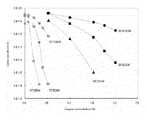
- FIG. 1is a graph showing a correlation among the oxygen concentration, the sputtering power and the film carrier density when sputtering is performed using the sintered oxide material according to the invention.
- the sintered oxide material for use in an embodiment of the inventionconsists essentially of indium (In), gallium (Ga), zinc (Zn), and oxygen (O) as constituent elements, wherein the ratio [In]/([In]+[Ga]) of the number of indium atoms to the total number of indium and gallium atoms is from 20% to 80%, and the ratio [Zn]/([In]+[Ga]+[Zn]) of the number of zinc atoms to the total number of indium, gallium and zinc atoms is from 10% to 50%, and the sintered oxide material has a specific resistance of 1.0 ⁇ 10 ⁇ 1 ⁇ cm or less.
- [In], [Ga] and [Zn]represent the number of indium atoms, the number of gallium atoms and the number of zinc atoms, respectively.
- the sintered oxide materialconsists essentially of In, Ga, Zn, and O as constituent elements.
- the term “essentially”means that the sintered oxide material of the invention may include an element or elements other than In, Ga, Zn, and O, such as an element(s) inevitably introduced during the process of purification of generally available materials or an inevitable impurity element(s) coming from the process of producing the sintered oxide material, at an inevitably occurring concentration such as up to about 10 ppm, as a constituent element or elements.
- the sintered oxide material according to the inventionalso satisfies the composition requirements that the ratio [In]/([In]+[Ga]) of the number of indium atoms to the total number of indium and gallium atoms is from 20% to 80% and that the ratio [Zn]/([In]+[Ga]+[Zn]) of the number of zinc atoms to the total number of indium, gallium and zinc atoms is from 10% to 50%.
- the composition requirementsare defined so that the film obtained by sputtering from a target made of the sintered oxide material having the composition can have a resistivity in the range where the film is suitable for use as a transparent semiconductor.
- An increase in the In ratiotends to result in an increase in the carrier density of the film obtained by sputtering from a target made of the sintered oxide material.
- an increase in the Ga ratiotends to result in a decrease in the carrier density of the film.
- the carrier density of the filmwill be too high, so that the on/off ratio (an important index of the device characteristics) of a thin film transistor produced with the film as an active layer may be degraded.
- [In]/([In]+[Ga])is less than 20%, the carrier density of the film will be too low in contrast to the above, so that the film may have low mobility, which is not preferred for the device characteristics.
- [Zn]/([In]+[Ga]+[Zn])is more than 50%, the stability, the humidity resistance and the like of the film may be degraded. If [Zn]/([In]+[Ga]+[Zn]) is less than 10%, the film formed by sputtering may be less amorphous and more likely to be crystalline. The crystallized film may have significant in-plane fluctuations in characteristics to cause fluctuations in device characteristics.
- the decrease in the Zn concentrationmeans an increase in the In or Ga concentration, which means an increase in the cost of the sintered oxide material itself, because these metals are relatively expensive.
- the sintered oxide materialmay be represented by InGaZnO 4
- the sintered oxide materialpreferably has a relative density of 95% or more. If the relative density of the sintered oxide material is less than 95%, the carrier density of the film may significantly vary, and the generation of nodules and the frequency of abnormal discharge may increase with the passage of sputtering time in the process of forming a film by sputtering using the sintered oxide material as a target, so that the resulting film may have degraded characteristics.
- the relative densityis preferably 97% or more, typically from 95 to 99%.
- a method for determining the relative density of the sintered oxide materialmay include determining the density of the sintered oxide material, which is assumed to have a relative density of 100%, from the respective constituent elements and the form for each composition, actually preparing the sintered oxide material and determining the density thereof by Archimedes' method or the like, and dividing the measurement by the density for 100% relative density to calculate the relative density.
- International Publication WO2005/088726 A1in which the production of a sintered In—Ga—Zn—O based oxide material is described, only discloses a relative density of 90% or more in the section of examples, and is completely silent on the production of a sintered oxide material with a relative density of 95% or more as disclosed herein.
- International Publication WO2005/088726 A1the need to increase the density of the sintered oxide material is not recognized at all, and it does not disclose or suggest any solution.
- the sintered oxide material prepared in International Publication WO2005/088726 A1has a density of 90% or more, which is not so high. This may be because the pulverizing time, the uniaxial compression pressure, or the like is not sufficient among the conditions of the production of the sintered oxide material.
- an a-IGZO filmcan be formed on a substrate by a sputtering method using the sintered oxide material as a sputtering target.
- the sputtering methodgenerally includes applying a voltage between the substrate as an anode and the sputtering target as a cathode in an argon gas atmosphere, so that argon cations in an argon plasma produced by glow discharge collide with the cathode sputtering target, from which particles are sputtered and deposited on the substrate to form a thin film.
- Sputtering methodsmay be classified into two types according to how to produce the argon plasma, and those using a radio-frequency plasma are called radio-frequency sputtering methods (RF sputtering methods), while those using a direct current plasma are called direct current sputtering methods (DC sputtering methods).
- a DC sputtering methodis used. This is because the controllability of the carrier density of the film is significantly improved, when DC sputtering is used.
- RFradio-frequency
- a slight change in the oxygen concentration of the atmosphere during the film productionmay cause a significant change in the carrier density.
- direct current sputteringhowever, as the oxygen concentration changes, the carrier density slowly changes, and therefore, strict control of the oxygen concentration is unnecessary.
- direct current sputtering methodshave advantages such as the ability to perform high-speed film production, inexpensive power supply systems, and easy operation including easy production of plasma, over radio-frequency sputtering methods.
- the direct current sputtering method as disclosed hereinmay also include a direct current pulsing method, which includes periodically stopping the voltage applied to a sputtering target and applying a low positive voltage for electrical neutralization.
- the sintered oxide material of the inventionis defined to have a specific resistance of 1.0 ⁇ 10 ⁇ 1 ⁇ cm or less and therefore suitable for use as a sputtering target in a direct current sputtering method.
- the specific resistance of the sintered oxide materialis not more than this value, the film production can be stably performed by direct current sputtering method.
- the specific resistanceis more preferably 1.0 ⁇ 10 ⁇ 2 ⁇ cm or less, so that the film production can be stably performed by direct current sputtering method under a considerably wide range of sputtering conditions.
- the sintered oxide materialtypically has a specific resistance of 1.2 ⁇ 10 ⁇ 4 to 4.0 ⁇ 10 ⁇ 4 ⁇ cm.
- the specific resistance of the sintered oxide materialmay be measured by four-terminal method or the like.
- the sintered oxide material according to the inventionmay be produced as described below.
- Indium oxide (In 2 O 3 ), gallium oxide (Ga 2 O 3 ) and zinc oxide (ZnO)may be used as raw materials.
- raw materials with a purity of 4N or higherare preferably used.
- Raw material powdersare each weighed so that the desired composition ratio can be achieved.
- each componentmay segregate in the produced target, so that a high resistivity region and a low resistivity region may occur, which may cause abnormal discharge such as arcing caused by electrification or the like in the high resistivity region during sputtering.
- sufficient mixingis necessary. Therefore, for example, raw materials are mixed in a super mixer at a speed of rotation of 2,000 to 4,000 rpm for a time period of 3 to 5 minutes in the air. Since the raw material powders are oxides, it is not necessary to prevent the oxidation of the raw materials, and therefore, the atmospheric gas may be air, with no need to use expensive gas such as argon.
- the mixing methodmay be a method of mixing in a ball mill for a long time or any other method capable of achieving the aim of uniformly mixing the raw materials.
- the mixed powderis then calcined in an electric furnace in the air atmosphere at a temperature in the range of 900 to 1,100° C. for a time period of about 4 to 6 hours.
- Pulverizationis then performed. Like the mixing of the raw materials, an object of the pulverization is to uniformly disperse the raw material powders into the target.
- the presence of large particle-size material powdermeans local unevenness in composition, which may cause abnormal discharge during sputtering.
- the calcined powderis placed together with zirconia beads in an attritor and pulverized at a speed of rotation of 200 to 400 rpm for a time period of 2 to 4 hours.
- the pulverizationis preferably performed until the average particle size (D50) of the raw material powder reaches 1 ⁇ m or less, preferably 0.6 ⁇ m or less.
- Granulationis then performed.
- An object of the granulationis to improve the fluidity of the raw material powder so that the packed state can be good enough during press molding.
- the water contentis controlled so that the pulverized raw materials can form a slurry with a solid content of 40 to 60%, when the granulation is performed.
- the inlet temperatureis set at 180 to 220° C.
- the outlet temperatureis set at 110 to 130° C.
- Press moldingis then performed.
- the granulated powderis subjected to press molding under the conditions of a surface pressure of 400 to 800 kgf/cm 2 and a holding time of 1 to 3 minutes. If the surface pressure is less than 400 kgf/cm 2 , it will be unable to obtain a molded product with a sufficiently high density. A surface pressure of more than 800 kgf/cm 2 is not necessary, and such a pressure is cost- or energy-consuming and not preferred for the production.
- the productis then formed in hydrostatic pressure equipment (CIP) under the conditions of a surface pressure of 1,700 to 1,900 kgf/cm 2 and a holding time of 1 to 3 minutes.
- CIPhydrostatic pressure equipment
- the productIn an electric furnace in an oxygen atmosphere, the product is then heated at a rate of 0.5 to 2.0° C./minute to 700 to 900° C., held for 4 to 6 hours, then heated at a rate of 0.5 to 5.0° C./minute to 1,300 to 1,500° C., then held for 10 to 30 hours, and then allowed to cool in the furnace or cooled at a rate of 2.0 to 5.0° C./minute. If the sintering temperature is lower than 1,300° C., the density of the sintered material cannot be high enough. On the other hand, if it is higher than 1,500° C., the life of the furnace heater may be reduced.
- the holding timeis shorter than 10 hours, the reaction between the raw material powders cannot sufficiently proceed, and the sintered material is not likely to have a sufficiently high density or can warp. If the sintering time is more than 30 hours, energy and time may be unnecessarily consumed, which is not preferred for the production. If the heating rate is less than 0.5° C./minute, time may be unnecessarily consumed until the desired temperature is reached. If the heating rate is more than 5.0° C./minute, the temperature distribution in the furnace may be unevenly raised, so that unevenness or cracking of the sintered material may occur.
- the sintered material obtained as described abovehas a relative density of about 95% or more and a specific resistance of 5.0 ⁇ 10 ⁇ 3 ⁇ cm or less, which depends on the composition.
- the sintered oxide material obtained by the production method described abovemay be subjected to cylindrical grinding of the rim and flat surface grinding of the face, so that it may be processed into a size suitable for the sputtering equipment to be used, such as a thickness of about 4 to 6 mm and a diameter of 6 inches.
- the processed materialmay be bonded to a backing copper plate with an indium-based alloy or the like as a bonding metal, so that the sputtering target can be obtained.
- the sputtering target produced by the method described above and a glass substrate or the likeare placed in a sputtering system, and the sputtering chamber is evacuated to a degree of vacuum of about 5 ⁇ 10 ⁇ 4 Pa or less by means of a rotary pump and a cryopump. If the degree of vacuum is insufficient, oxygen or water may remain in the chamber and be introduced into a film during sputtering to have an adverse effect on the electrical characteristics of the film.
- a gas mixture of argon and oxygenmay be used as the sputtering gas.
- a method for controlling the concentration of oxygen in the gas mixturemay include providing a 100% argon gas cylinder and a gas cylinder containing argon and 2% oxygen therein and appropriately setting the flow rate of the gas supplied from each gas cylinder to the chamber by controlling the mass flow.
- the concentration of oxygen in the gas mixturemeans the ratio: oxygen partial pressure/(oxygen partial pressure+argon partial pressure), which is also equal to the quotient obtained by dividing the oxygen flow rate by the total flow rate of oxygen and argon.
- the oxygen concentrationmay be changed as needed according to the desired carrier density, it may be typically from 1 to 3%, more typically from 1 to 2%.
- the total pressure of the sputtering gasmay be from about 0.3 to 0.8 Pa. If the total pressure is lower than this range, it may be difficult to establish plasma discharge, or established plasma discharge may be unstable. If the total pressure is higher than this range, the deposition rate may become lower, so that a problem such as an adverse effect on the productivity may occur.
- Plasma generation methodsinclude both a radio-frequency (RF) sputtering method and a direct current (DC) sputtering method. For the purpose of simply producing a film, both methods may be used.
- the radio-frequency (RF) sputtering methodcan be performed regardless of the specific resistance of the target, for example, even with a dielectric target.
- the direct current (DC) sputtering methodrequires the target to have a specific resistance of a certain value or less, such as 1 ⁇ 10 ⁇ 1 ⁇ cm or less.
- the sintered oxide materialhas such a low level of specific resistance that direct current (DC) sputtering is possible, and therefore makes it possible to use direct current (DC) sputtering method.
- direct current (DC) sputtering methodis used for sputtering deposition in order to obtain films with a constant carrier density with high reproducibility.
- the distance between the target and the substrateshould be set at 70 to 120 mm. If the distance is too short, particles of the constituent elements of the target may have too high kinetic energy when arriving at the substrate, so that the substrate may be severely damaged, which makes it unable to obtain good film properties, degrading the in-plane distribution of the electrical characteristics of the film or the thickness of the film. If the distance is too long, particles of the constituent elements of the target may have too low kinetic energy when arriving at the substrate, so that it may be unable to form a dense film or obtain good film properties.
- the filmcan be produced by sputtering without heating the substrate.
- the temperature of the substratemay be from about 25 to 50° C. (sputtering-induced temperature rises or so). This is advantageous in that energy or time for heating the substrate is not necessary, and the most advantageous point is that materials other than glass can also be used for the substrate.
- a resin material that cannot withstand high temperaturemay be used as the substrate.
- the substrateis preferably transparent. Examples of such a material include polyethylene terephthalate (PET), polyethersulfone (PES), polyethylene naphthalate (PEN), polycarbonate (PC), and polyarylate (PAR).
- PETpolyethylene terephthalate
- PESpolyethersulfone
- PENpolyethylene naphthalate
- PCpolycarbonate
- PARpolyarylate
- a filmmay be deposited thereon to improve the adhesion or prevent degassing.
- the sputtering poweris preferably from 500 to 1,200 W, which may be converted to a sputtering power density of about 2.7 W/cm 2 to 6.6 W/cm 2 , preferably 3.2 to 4.5 W/cm 2 .
- the sputtering power densityis the quotient obtained by dividing the sputtering power by the area of the sputtering target. Even at the same power, the power actually received by the sputtering target and the deposition rate vary with the size of the target. Therefore, the sputtering power density may be used as an index for indicating the power applied to the sputtering target in a standardized manner.
- the carrier density of the film deposited by sputteringmay be significantly dependent on the oxygen concentration. This means that even a slight change in the oxygen concentration may cause a significant change in the carrier density, so that it may be difficult to obtain films with a constant carrier density with high reproducibility. If the sputtering power density is more than 6.6 W/cm 2 , the deposition rate may become so high that the film thickness controllability may be degraded. Therefore, even if the deposition time is controlled to be constant by opening and closing a shutter in the same manner, the film thickness may significantly change by a slight difference in time period when the shutter is opened and closed.
- the above appropriate range of the sputtering powermay correspond to a deposition rate of about 2.5 ⁇ /second to 5.5 ⁇ /second under normal sputtering conditions.
- the deposition ratemay be used for the control.
- the deposition rate of sputteringis the quotient obtained by dividing the film thickness by the deposition time period, which is proportional to the sputtering power density under the normal range of deposition conditions.
- the deposition rateshould be in the above range for the same reason as that for the sputtering power range defined above, namely, in order that the controllability of the carrier density and the controllability of the film thickness may be established at the same time.
- the deposition rateis preferably from about 3.0 ⁇ /second to 4.5 ⁇ /second.
- the film formed without heating the substrateis generally an a-IGZO film.
- the a-IGZO filmhas a flat surface and high in-plane uniformity and does not have grain boundaries as in a polycrystalline film. Therefore, the a-IGZO film is advantageous in that when the film is used as an active layer to form a device, variations in the device characteristics can be reduced to a very low level.
- the thickness of the film obtained by sputteringmay be measured with a step profiler.
- the carrier density of the filmmay be determined by Hall measurement according to the Van der Pauw method. Specifically, the film-carrying glass substrate or the like is cut into an about 10 mm square piece. Electrodes of indium or the like are attached to the four corners of the piece, and the piece is placed in the Hall measurement system so that the resistivity, carrier density and mobility of the film can be measured. Whether the film is amorphous or not may be determined by X-ray diffraction system. The composition of the film may be measured by fluorescent X-ray analysis.
- the method for annealing the oxide thin filmis described below.
- the glass substrate carrying the film obtained by sputteringis placed in a furnace whose temperature can be set at a predetermined value.
- the airis evacuated from the furnace by means of a rotary pump or the like, and then pure oxygen or a specific type of gas with a predetermined concentration is introduced into the furnace.
- a predetermined temperaturegenerally 100 to 600° C., preferably 200 to 400° C.
- the temperatureis held for a certain period of time (generally 1 to 60 minutes, preferably 1 to 20 minutes because the effect of annealing may be saturated, if it is performed for too long a period of time), after which the temperature is lowered, thereby annealing the oxide thin film.
- a certain period of timegenerally 1 to 60 minutes, preferably 1 to 20 minutes because the effect of annealing may be saturated, if it is performed for too long a period of time
- An important thing in this processis to evacuate the air from the furnace in which the oxide thin film is placed. If the evacuation is insufficient, annealing cannot be performed in a specific type of gas with a predetermined concentration and may be affected by residual oxygen or nitrogen in the atmosphere.
- the carrier density of the a-IGZO filmis controlled by the oxygen deficiency in the film. Therefore, when annealing is performed in an oxygen-containing gas atmosphere, the oxygen deficiency can be eliminated from the film, so that the carrier density of the film can be reduced or controlled. On the other hand, when annealing is performed in an oxygen-free gas atmosphere such as nitrogen, the oxygen deficiency in the film may further develop and increase the carrier density.
- the carrier densitytends to converge to a constant value, depending on the concentration of oxygen in the atmosphere gas, and therefore, variations in the carrier density of the film per lot can be further reduced. The carrier density is more likely to converge to a constant value when the oxygen concentration is high than when it is low.
- the concentration of oxygen in the atmosphere during annealingis typically 25% by volume or more, more typically 50% by volume or more, further typically 100% by volume, so that variations in the carrier density can be more effectively reduced.
- the oxide thin film obtained using the production method according to an embodiment of the inventionmay be used as an active layer for a thin film transistor.
- the thin film transistor obtained using the above production methodmay be used as an active device to form an active matrix driving display panel.
- the actual densitywas measured by Archimedes' method, and the relative density was calculated by dividing the actual density by the theoretical density determined from the constituent elements.
- the sintered materialwas cut into a piece, and the specific resistance of the cut piece was determined by Hall measurement using Model RESITEST 8200 manufactured by TOYO Corporation.
- the crystal structure of the sintered materialwas analyzed using an X-ray diffraction system (Model RINT-1100 manufactured by Rigaku Corporation).
- the composition of the sintered materialwas determined by ICP (inductively coupled plasma) analysis using Model SPS3000 manufactured by SII Nano Technology Inc.
- the film thicknesswas determined using a step profiler (Model Dektak 8 STYLUS PROFILER, manufactured by Veeco Instruments).
- the film-carrying glass substratewas cut into an about 10 mm square piece, and indium electrodes were attached to four corners of the cut piece.
- the cut piecewas placed in a Hall measurement system (Model Resitest 8200 manufactured by TOYO Corporation), and the measurement was performed.
- the crystallinitywas determined using an X-ray diffraction system RINT-1100 manufactured by Rigaku Corporation.
- composition of the filmwas determined by ICP (inductively coupled plasma) analysis using Model SPS3000 manufactured by SII Nano Technology Inc.
- Indium oxide (In 2 O 3 ), gallium oxide (Ga 2 O 3 ) and zinc oxide (ZnO) powders as raw materialswere each weighed so that the metal element composition ratio In:Ga:Zn could be 1:1:1.
- the weighed raw material powderswere mixed in a super mixer at a speed of rotation of 3,000 rpm for a time period of 4 minutes in the air.
- the mixed powderwas held in an electric furnace at 1,000° C. for 5 hours in the atmosphere.
- the calcined powderwas placed together with zirconia beads in an attritor and pulverized at a speed of rotation of 300 rpm for a time period of 3 hours. In the pulverization, the average particle size (D50) of the raw material powder reached 0.59 ⁇ m.
- the water contentwas controlled so that the pulverized raw material powder could form a slurry with a solid content of 50%, and granulation was performed with the inlet temperature set at 200° C. and the outlet temperature set at 120° C.
- the granulated powderwas subjected to press molding under the conditions of a surface pressure of 400 kgf/cm 2 and a holding time of 1 minute and then formed in hydrostatic pressure equipment (CIP) under the conditions of a surface pressure of 1,800 kgf/cm 2 and a holding time of 1 minute.
- CIPhydrostatic pressure equipment
- the productwas heated at a rate of 1.0° C./minute to 800° C., then held for 5 hours, then heated at a rate of 1.0° C./minute to 1,450° C., then held for 20 hours, and then allowed to cool in the electric furnace in the oxygen atmosphere.
- the resulting sintered materialhad a relative density of about 98% and a specific resistance of 3.2 ⁇ 10 ⁇ 3 ⁇ cm.
- the sintered materialwas found to be a crystalline oxide having a composition represented by the formula: InGaZnO 4 .
- a sintered oxide materialwas prepared under almost the same conditions as in Example 1-1 except for the following modification of the conditions.
- the time of pulverization of the calcined powder in the attritorwas changed to 1 hour, the granulated powder was pressed under a surface pressure of 100 kgf/cm 2 , and press forming in the hydrostatic pressure equipment (CIP) was not performed.
- the resulting sintered materialhad a relative density of about 80% and a specific resistance of 4.0 ⁇ cm.
- the sintered materialwas found to be a crystalline oxide having a composition represented by the formula: InGaZnO 4 .
- a sintered oxide materialwas prepared under almost the same conditions as in Example 1-1 except for the following modification of the conditions.
- the granulated powderwas pressed under a surface pressure of 200 kgf/cm 2 , and press forming in the hydrostatic pressure equipment (CIP) was not performed.
- the resulting sintered materialhad a relative density of about 85% and a specific resistance of 3.9 ⁇ cm.
- the sintered materialwas found to be a crystalline oxide having a composition represented by the formula: InGaZnO 4 .
- a sintered oxide materialwas prepared under almost the same conditions as in Example 1-1 except for the following modification of the conditions.
- the surface pressure in the hydrostatic pressure equipment (CIP)was changed to 900 kgf/cm 2 .
- the resulting sintered materialhad a relative density of about 92% and a specific resistance of 3.8 ⁇ cm.
- the sintered materialwas found to be a crystalline oxide having a composition represented by the formula: InGaZnO 4 .
- the sintered oxide material prepared under the oxide sintering conditions in Example 1-1had the intended density and specific resistance. However, the sintered oxide materials prepared under the oxide sintering conditions in the comparative examples did not have a sufficient sintered density.
- the sintered material prepared by the method described in Example 1-1was worked into a disc with a diameter of 6 inches and a thickness of 5 mm, which was used as a sputtering target.
- the sputtering target and a Corning #1737 glass substrate with a diameter of 4 inches and a thickness of 0.7 mmwere placed in a sputtering system, and the sputtering chamber was evacuated to a degree of vacuum of about 5 ⁇ 10 ⁇ 4 Pa or less by means of a rotary pump and a cryopump.
- each of pure argon gas and argon gas containing 2% oxygenwas controlled by a mass flow controller, so that sputtering gas with an oxygen concentration of 2.0% was introduced into the chamber.
- the total pressure of the sputtering gas in the chamberwas set at 0.5 Pa.
- a direct current (DC) sputtering methodwas used with a sputtering power of 1,000 W and a target-substrate distance of 80 mm. The substrate was not heated.
- the depositionwas performed at a rate of 5.29 ⁇ /second for a time period of 197 seconds to form a film with a thickness of 1,043 ⁇ .
- the filmhad a carrier density of 1.79 ⁇ 10 18 cm ⁇ 3 , a mobility of 9.35 cm 2 /Vs, and a resistivity of 3.74 ⁇ 10 ⁇ 1 ⁇ cm.
- the filmhad a composition of InGaZnO 4 and was amorphous. The conditions and the results are shown in Table 1.
- the oxide thin films of Examples 2-2 to 2-10were produced using the sintered material prepared by the method described in Example 1-1 as a sputtering target under the same conditions as in Example 2-1 except for the modifications of the conditions shown in Table 1. All the films had a composition of InGaZnO 4 and were amorphous. The results of the measurement of the electrical characteristics of the films are also shown in Table 1.
- the oxide thin films of Comparative Examples 2-1 to 2-3were produced using the sintered material prepared by the method described in Example 1-1 as a sputtering target under the same conditions as in Example 2-1 except for the modifications of the conditions shown in Table 1. All the films had a composition of InGaZnO 4 and were amorphous. The results of the measurement of the electrical characteristics of the films are also shown in Table 1.
- the oxide thin films of Comparative Examples 2-4 to 2-19were produced using the sintered material prepared by the method described in Example 1-1 as a sputtering target under the same conditions as in Example 2-1, except that the power source type was changed to a radio-frequency (RF) type and that some conditions were modified as shown in Table 1. All the films had a composition of InGaZnO 4 and were amorphous. The results of the measurement of the electrical characteristics of the films are also shown in Table 1.
- FIG. 1is a graph showing the results of the examples, in which the horizontal axis represents the oxygen concentration, and the vertical axis represents the carrier density of the film.
- the carrier density of the filmtends to increase with increasing sputtering power.
- the case of direct current sputteringshows that when the oxygen concentration is relatively low, a difference in sputtering power makes a small difference in the carrier density of the film, but when the oxygen concentration is relatively high, a difference in sputtering power makes a significant difference in the carrier density of the film. In this case, therefore, a film with a predetermined carrier density can be obtained by controlling the sputtering power during the sputtering as well as by controlling the oxygen concentration.
- the oxygen concentration-dependency of the carrier density of the filmdecreases with increasing sputtering power. This means that the process of forming a film with a specific carrier density can become less susceptible to the change in the oxygen concentration so that the controllability of the carrier density can be improved.
- the controllability of the carrier densityis not so improved, and a slight change in the oxygen concentration may cause a significant change in the carrier density.
- the direct current sputteringis performed at high sputtering power, the controllability of the carrier density of the film can be most improved.
- An oxide thin filmwas produced using the sintered material described in Example 1-1 as a sputtering target under the same deposition conditions as in Example 2-1, except that the oxygen concentration was changed to 1.5%.
- the glass substrate carrying the film obtained by the sputteringwas placed in an annealing furnace.
- the furnacewas evacuated from the atmospheric pressure to 1 ⁇ 10 ⁇ 2 Pa by means of a rotary pump or the like. Pure oxygen gas was then introduced into the furnace, and the oxide thin film was annealed by a process including heating the film to the predetermined temperature of 300° C. in about 1 minute, then maintaining the temperature for 10 minutes, and then allowing the film to cool in the furnace.
- the carrier density of the filmwas 8.0 ⁇ 10 18 cm ⁇ 3 before the annealing and 9.8 ⁇ 10 16 cm ⁇ 3 after the annealing.
- oxide thin films with two different carrier densitieswere prepared using the deposition conditions of Example 3-1, except that the oxygen concentration was changed to 0.8% and 0%, so that three types of oxide thin films were prepared in total. These oxide thin films were annealed under different conditions as shown in Table 2. The carrier densities of the annealed films are as shown in Table 2.
- the carrier densities of the filmsvary to a certain extent before annealing, the carrier densities of the films are reduced and made less variable by annealing in an atmosphere of oxygen or a mixture of 50% by volume of oxygen and 50% by volume of nitrogen.
- the atmosphere gasis oxygen
- the carrier densitiesbecome close to one another.
- annealing in a nitrogen atmosphereincreases the oxygen deficiency, so that the carrier density becomes higher than that before the annealing.
Landscapes
- Engineering & Computer Science (AREA)
- Chemical & Material Sciences (AREA)
- Manufacturing & Machinery (AREA)
- Ceramic Engineering (AREA)
- Materials Engineering (AREA)
- Organic Chemistry (AREA)
- Structural Engineering (AREA)
- Microelectronics & Electronic Packaging (AREA)
- Power Engineering (AREA)
- General Physics & Mathematics (AREA)
- Computer Hardware Design (AREA)
- Physics & Mathematics (AREA)
- Condensed Matter Physics & Semiconductors (AREA)
- Inorganic Chemistry (AREA)
- Chemical Kinetics & Catalysis (AREA)
- Metallurgy (AREA)
- Mechanical Engineering (AREA)
- Crystallography & Structural Chemistry (AREA)
- Physical Vapour Deposition (AREA)
- Thin Film Transistor (AREA)
- Physical Deposition Of Substances That Are Components Of Semiconductor Devices (AREA)
Abstract
Description
| TABLE 1 | ||||||||||
| Power | Power | Oxygen | Carrier | Film | Deposition | |||||
| source | Power | density | concentration | density | Mobility | Resistivity | thickness | Time | rate | |
| type | (W) | (W/cm2) | (%) | (cm−3) | (cm2/Vs) | (Ω cm) | (Å) | (seconds) | (Å/sec) | |
| Example 2-1 | DC | 1000 | 5.48 | 2.00 | 1.79 × 10¹⁸ | 9.35 | 3.74 × 10⁻¹ | 1043 | 197 | 5.29 |
| Example 2-2 | DC | 1000 | 5.48 | 1.76 | 4.32 × 10¹⁸ | 10.10 | 1.43 × 10⁻¹ | 1010 | 189 | 5.34 |
| Example 2-3 | DC | 1000 | 5.48 | 1.52 | 8.02 × 10¹⁸ | 12.50 | 6.26 × 10⁻² | 1007 | 187 | 5.39 |
| Example 2-4 | DC | 1000 | 5.48 | 1.00 | 1.75 × 10¹⁹ | 12.00 | 2.96 × 10⁻² | 997 | 187 | 5.33 |
| Example 2-5 | DC | 1000 | 5.48 | 0.52 | 4.04 × 10¹⁹ | 11.10 | 1.39 × 10⁻² | 1020 | 188 | 5.43 |
| Example 2-6 | DC | 500 | 2.74 | 2.00 | 5.60 × 10¹⁵ | 4.98 | 2.24 × 10² | 1017 | 394 | 2.58 |
| Example 2-7 | DC | 500 | 2.74 | 1.76 | 4.51 × 10¹⁶ | 7.59 | 1.83 × 101 | 993 | 378 | 2.63 |
| Example 2-8 | DC | 500 | 2.74 | 1.52 | 5.17 × 10¹⁷ | 9.73 | 1.24 × 100 | 997 | 373 | 2.67 |
| Example 2-9 | DC | 500 | 2.74 | 1.00 | 5.99 × 10¹⁸ | 11.10 | 9.36 × 10⁻² | 1010 | 379 | 2.66 |
| Example 2-10 | DC | 500 | 2.74 | 0.52 | 3.89 × 10¹⁹ | 10.40 | 1.54 × 10⁻² | 1013 | 376 | 2.69 |
| Comparative | DC | 250 | 1.37 | 1.52 | 1.06 × 10¹⁵ | 5.90 | 1.00 × 10³ | 965 | 742 | 1.30 |
| Example 2-1 | ||||||||||
| Comparative | DC | 250 | 1.37 | 1.00 | 4.13 × 10¹⁷ | 9.10 | 1.66 × 100 | 944 | 706 | 1.34 |
| Example 2-2 | ||||||||||
| Comparative | DC | 250 | 1.37 | 0.52 | 1.10 × 10¹⁹ | 11.10 | 5.09 × 10⁻² | 952 | 702 | 1.36 |
| Example 2-3 | ||||||||||
| Comparative | RF | 1000 | 5.48 | 0.50 | 6.67 × 10¹⁷ | 11.80 | 7.92 × 10⁻¹ | 1006 | 365 | 2.76 |
| Example 2-4 | ||||||||||
| Comparative | RF | 1000 | 5.48 | 0.40 | 2.82 × 10¹⁸ | 9.87 | 2.25 × 10⁻¹ | 1006 | 356 | 2.83 |
| Example 2-5 | ||||||||||
| Comparative | RF | 1000 | 5.48 | 0.32 | 6.42 × 10¹⁸ | 12.10 | 8.08 × 10⁻² | 1039 | 361 | 2.88 |
| Example 2-6 | ||||||||||
| Comparative | RF | 1000 | 5.48 | 0.20 | 1.69 × 10¹⁹ | 12.10 | 8.08 × 10⁻² | 976 | 338 | 2.89 |
| Example 2-7 | ||||||||||
| Comparative | RF | 1000 | 5.48 | 0.08 | 2.78 × 10¹⁹ | 11.10 | 1.97 × 10⁻² | 1023 | 357 | 2.87 |
| Example 2-8 | ||||||||||
| Comparative | RF | 1000 | 5.48 | 0.00 | 3.17 × 10¹⁹ | 7.08 | 2.79 × 10⁻² | 969 | 328 | 2.95 |
| Example 2-9 | ||||||||||
| Comparative | RF | 500 | 2.74 | 0.50 | 1.30 × 10¹⁴ | 2.88 | 1.67 × 10⁴ | 1013 | 730 | 1.39 |
| Example 2-10 | ||||||||||
| Comparative | RF | 500 | 2.74 | 0.40 | 2.41 × 10¹⁵ | 11.70 | 2.21 × 10² | 1005 | 713 | 1.41 |
| Example 2-11 | ||||||||||
| Comparative | RF | 500 | 2.74 | 0.32 | 2.13 × 10¹⁷ | 9.09 | 3.22 × 100 | 1071 | 722 | 1.48 |
| Example 2-12 | ||||||||||
| Comparative | RF | 500 | 2.74 | 0.20 | 3.64 × 10¹⁸ | 11.80 | 1.45 × 10⁻¹ | 1000 | 676 | 1.48 |
| Example 2-13 | ||||||||||
| Comparative | RF | 500 | 2.74 | 0.08 | 2.26 × 10¹⁹ | 11.70 | 2.36 × 10⁻² | 1068 | 714 | 1.50 |
| Example 2-14 | ||||||||||
| Comparative | RF | 500 | 2.74 | 0.00 | 2.40 × 10¹⁹ | 11.70 | 2.23 × 10⁻² | 989 | 656 | 1.51 |
| Example 2-15 | ||||||||||
| Comparative | RF | 250 | 1.37 | 0.40 | 1.29 × 10¹⁴ | 15.10 | 3.20 × 10³ | 490 | 722 | 0.68 |
| Example 2-16 | ||||||||||
| Comparative | RF | 250 | 1.37 | 0.32 | 8.44 × 10¹⁵ | 10.40 | 7.14 × 101 | 480 | 676 | 0.71 |
| Example 2-17 | ||||||||||
| Comparative | RF | 250 | 1.37 | 0.08 | 9.25 × 10¹⁸ | 12.70 | 5.30 × 10⁻² | 522 | 714 | 0.73 |
| Example 2-18 | ||||||||||
| Comparative | RF | 250 | 1.37 | 0.00 | 6.95 × 10¹⁸ | 13.80 | 6.51 × 10⁻² | 477 | 656 | 0.73 |
| Example 2-19 | ||||||||||
| TABLE 2 | |||||
| Carrier | Carrier | ||||
| Annealing | density | density | |||
| temper- | Annealing | (cm−3) | (cm−3) | ||
| Annealing | ature | time | before | after | |
| atmosphere | (° C.) | (minutes) | annealing | annealing | |
| Example | Oxygen | 300 | 10 | 8.1 × 10¹⁸ | 9.9 × 10¹⁶ |
| 3-1 | |||||
| Example | Oxygen | 300 | 10 | 2.0 × 10¹⁹ | 1.0 × 10¹⁷ |
| 3-2 | |||||
| Example | Oxygen | 300 | 10 | 6.0 × 10¹⁹ | 1.1 × 10¹⁷ |
| 3-3 | |||||
| Example | Oxygen 50%, | 300 | 10 | 8.1 × 10¹⁸ | 7.6 × 10¹⁷ |
| 3-4 | Nitrogen 50% | ||||
| Example | Oxygen 50%, | 300 | 10 | 2.0 × 10¹⁹ | 8.0 × 10¹⁷ |
| 3-5 | Nitrogen 50% | ||||
| Example | Oxygen 50%, | 300 | 10 | 6.0 × 10¹⁹ | 8.3 × 10¹⁷ |
| 3-6 | Nitrogen 50% | ||||
| Example | Nitrogen | 300 | 10 | 8.1 × 10¹⁸ | 2.3 × 10¹⁹ |
| 3-7 | |||||
| Example | Nitrogen | 300 | 10 | 2.0 × 10¹⁹ | 2.6 × 10¹⁹ |
| 3-8 | |||||
| Example | Nitrogen | 300 | 10 | 6.0 × 10¹⁹ | 6.1 × 10¹⁹ |
| 3-9 | |||||
Claims (10)
Applications Claiming Priority (3)
| Application Number | Priority Date | Filing Date | Title |
|---|---|---|---|
| JP2007-336398 | 2007-12-27 | ||
| JP2007336398 | 2007-12-27 | ||
| PCT/JP2008/073439WO2009084537A1 (en) | 2007-12-27 | 2008-12-24 | Process for producing thin film of a-igzo oxide |
Publications (2)
| Publication Number | Publication Date |
|---|---|
| US20110306165A1 US20110306165A1 (en) | 2011-12-15 |
| US8148245B2true US8148245B2 (en) | 2012-04-03 |
Family
ID=40824251
Family Applications (1)
| Application Number | Title | Priority Date | Filing Date |
|---|---|---|---|
| US12/743,593ActiveUS8148245B2 (en) | 2007-12-27 | 2008-12-24 | Method for producing a-IGZO oxide thin film |
Country Status (6)
| Country | Link |
|---|---|
| US (1) | US8148245B2 (en) |
| JP (1) | JP5345952B2 (en) |
| KR (1) | KR101228160B1 (en) |
| CN (1) | CN101910450B (en) |
| TW (1) | TWI410509B (en) |
| WO (1) | WO2009084537A1 (en) |
Cited By (26)
| Publication number | Priority date | Publication date | Assignee | Title |
|---|---|---|---|---|
| US20100182223A1 (en)* | 2009-01-22 | 2010-07-22 | Samsung Mobile Display Co., Ltd. | Organic light emitting display device |
| US20100300878A1 (en)* | 2008-06-10 | 2010-12-02 | Nippon Mining & Metals Co., Ltd. | Sintered Oxide Compact Target for Sputtering and Process for Producing the same |
| US20110008931A1 (en)* | 2009-07-10 | 2011-01-13 | Semiconductor Energy Laboratory Co., Ltd. | Method for manufacturing semiconductor device |
| US20110068336A1 (en)* | 2009-09-24 | 2011-03-24 | Semiconductor Energy Laboratory Co., Ltd. | Semiconductor element and method for manufacturing the same |
| US20110079778A1 (en)* | 2009-10-05 | 2011-04-07 | Semiconductor Energy Laboratory Co., Ltd. | Semiconductor device and manufacturing method thereof |
| US20120103804A1 (en)* | 2009-06-05 | 2012-05-03 | Jx Nippon Mining & Metals Corporation | Oxide Sintered Compact, Its Production Method, and Raw Material Powder for Producing Oxide Sintered Compact |
| US20120228608A1 (en)* | 2009-11-19 | 2012-09-13 | Koki Yano | Sputtering target and thin film transistor equipped with same |
| US20140014500A1 (en)* | 2011-03-24 | 2014-01-16 | Idemitsu Kosan Co., Ltd. | Sintered material, and process for producing same |
| US8841163B2 (en) | 2009-12-04 | 2014-09-23 | Semiconductor Energy Laboratory Co., Ltd. | Manufacturing method of semiconductor device comprising oxide semiconductor |
| US20140370657A1 (en)* | 2011-03-11 | 2014-12-18 | Semiconductor Energy Laboratory Co., Ltd. | Method of manufacturing semiconductor device |
| US9054137B2 (en) | 2009-06-30 | 2015-06-09 | Semiconductor Energy Laboratory Co., Ltd. | Method for manufacturing semiconductor device |
| US20150200208A1 (en)* | 2014-01-10 | 2015-07-16 | Samsung Display Co., Ltd. | Thin film transistor array panel and method for manufacturing the same |
| US9093262B2 (en) | 2009-11-20 | 2015-07-28 | Semiconductor Energy Laboratory Co., Ltd. | Method for manufacturing semiconductor device |
| US9153702B2 (en) | 2009-09-24 | 2015-10-06 | Semiconductor Energy Laboratory Co., Ltd. | Semiconductor device, power circuit, and manufacturing method of semiconductor device |
| US9224838B2 (en) | 2009-09-24 | 2015-12-29 | Semiconductor Energy Laboratory Co., Ltd. | Method for manufacturing oxide semiconductor film and method for manufacturing semiconductor device |
| US9384976B2 (en) | 2009-11-06 | 2016-07-05 | Semiconductor Energy Laboratory Co., Ltd. | Method for manufacturing semiconductor device |
| US9767998B2 (en) | 2011-09-06 | 2017-09-19 | Idemitsu Kosan Co., Ltd. | Sputtering target |
| TWI613824B (en)* | 2011-12-23 | 2018-02-01 | 半導體能源研究所股份有限公司 | Semiconductor device |
| US9905596B2 (en) | 2009-11-06 | 2018-02-27 | Semiconductor Energy Laboratory Co., Ltd. | Semiconductor device comprising a channel region of a transistor with a crystalline oxide semiconductor and a specific off-state current for the transistor |
| US10002949B2 (en) | 2009-11-06 | 2018-06-19 | Semiconductor Energy Laboratory Co., Ltd. | Semiconductor device |
| US10047012B2 (en) | 2015-03-23 | 2018-08-14 | Jx Nippon Mining & Metals Corporation | Oxide sintered compact and sputtering target formed from said oxide sintered compact |
| US10161031B2 (en) | 2015-02-27 | 2018-12-25 | Jx Nippon Mining & Metals Corporation | Oxide sintered compact and sputtering target formed from said oxide sintered compact |
| US10186603B2 (en) | 2010-05-21 | 2019-01-22 | Semiconductor Energy Laboratory Co., Ltd. | Manufacturing method of semiconductor device including oxygen doping treatment |
| US10205008B2 (en) | 2016-08-03 | 2019-02-12 | Semiconductor Energy Laboratory Co., Ltd. | Manufacturing method of semiconductor device |
| US10566459B2 (en) | 2009-10-30 | 2020-02-18 | Semiconductor Energy Laboratory Co., Ltd. | Semiconductor device having a first region comprising silicon, oxygen and at least one metal element formed between an oxide semiconductor layer and an insulating layer |
| US10692994B2 (en) | 2016-12-23 | 2020-06-23 | Semiconductor Energy Laboratory Co., Ltd. | Semiconductor device and method for manufacturing the same |
Families Citing this family (32)
| Publication number | Priority date | Publication date | Assignee | Title |
|---|---|---|---|---|
| JP5683179B2 (en)* | 2009-09-24 | 2015-03-11 | 株式会社半導体エネルギー研究所 | Method for manufacturing display device |
| KR102219095B1 (en)* | 2009-09-24 | 2021-02-23 | 가부시키가이샤 한도오따이 에네루기 켄큐쇼 | Semiconductor device and method for manufacturing the same |
| KR20120093952A (en)* | 2009-11-06 | 2012-08-23 | 가부시키가이샤 한도오따이 에네루기 켄큐쇼 | Method for manufacturing semiconductor element and semiconductor device, and deposition apparatus |
| JP4891381B2 (en) | 2009-11-19 | 2012-03-07 | 出光興産株式会社 | In-Ga-Zn-based sintered body and sputtering target |
| JP4843083B2 (en) | 2009-11-19 | 2011-12-21 | 出光興産株式会社 | In-Ga-Zn-based oxide sputtering target |
| JP5591523B2 (en)* | 2009-11-19 | 2014-09-17 | 出光興産株式会社 | In-Ga-Zn-O-based oxide sintered sputtering target excellent in stability during long-term film formation |
| JP5844030B2 (en)* | 2010-01-14 | 2016-01-13 | 富士フイルム株式会社 | Field effect transistor manufacturing method, display device manufacturing method, X-ray imaging device manufacturing method, and optical sensor manufacturing method |
| JP5437825B2 (en) | 2010-01-15 | 2014-03-12 | 出光興産株式会社 | In-Ga-O-based oxide sintered body, target, oxide semiconductor thin film, and production method thereof |
| JP5560064B2 (en)* | 2010-03-03 | 2014-07-23 | 富士フイルム株式会社 | IGZO amorphous oxide thin film manufacturing method and field effect transistor manufacturing method using the same |
| CN102834921B (en)* | 2010-03-26 | 2016-04-27 | 株式会社半导体能源研究所 | Manufacturing method of semiconductor device |
| JP4962587B2 (en)* | 2010-03-29 | 2012-06-27 | Tdk株式会社 | Sputtering target, sputtering target manufacturing method, and optical media manufacturing method |
| JP2012124446A (en)* | 2010-04-07 | 2012-06-28 | Kobe Steel Ltd | Oxide for semiconductor layer of thin film transistor and sputtering target, and thin film transistor |
| JPWO2011132418A1 (en)* | 2010-04-22 | 2013-07-18 | 出光興産株式会社 | Deposition method |
| WO2011145537A1 (en)* | 2010-05-21 | 2011-11-24 | Semiconductor Energy Laboratory Co., Ltd. | Liquid crystal display device |
| JP2012052227A (en)* | 2010-08-05 | 2012-03-15 | Mitsubishi Materials Corp | Method for manufacturing sputtering target, and sputtering target |
| JP5525380B2 (en)* | 2010-08-25 | 2014-06-18 | 富士フイルム株式会社 | Method for manufacturing oxide semiconductor thin film and method for manufacturing thin film transistor |
| DE102010047756B3 (en)* | 2010-10-08 | 2012-03-01 | Heraeus Materials Technology Gmbh & Co. Kg | Sputtering target, useful for sputter deposition, comprises a mixture of oxides of indium, zinc and gallium and a ternary mixed oxide of indium, zinc and gallium |
| CN102694053B (en)* | 2011-03-22 | 2015-08-05 | 中国科学院微电子研究所 | Semiconductor device and method for manufacturing the same |
| CN102694052B (en)* | 2011-03-22 | 2016-01-06 | 中国科学院微电子研究所 | Semiconductor device and method for manufacturing the same |
| US9039944B2 (en) | 2011-07-06 | 2015-05-26 | Idemitsu Kosan Co., Ltd. | Sputtering target |
| KR101402961B1 (en)* | 2012-03-20 | 2014-06-03 | (주)이루자 | Sputtering apparatus for a-IGZO thin film deposition, and methods of manufacturing substrate for electronic device and display device using the same |
| JP5965338B2 (en) | 2012-07-17 | 2016-08-03 | 出光興産株式会社 | Sputtering target, oxide semiconductor thin film, and manufacturing method thereof |
| JP5998712B2 (en)* | 2012-07-30 | 2016-09-28 | 東ソー株式会社 | IGZO sintered body, sputtering target, and oxide film |
| JP6284710B2 (en) | 2012-10-18 | 2018-02-28 | 出光興産株式会社 | Sputtering target, oxide semiconductor thin film, and manufacturing method thereof |
| WO2014073585A1 (en)* | 2012-11-08 | 2014-05-15 | Semiconductor Energy Laboratory Co., Ltd. | Metal oxide film and method for forming metal oxide film |
| JP6059513B2 (en) | 2012-11-14 | 2017-01-11 | 出光興産株式会社 | Sputtering target, oxide semiconductor thin film, and manufacturing method thereof |
| TWI631711B (en) | 2013-05-01 | 2018-08-01 | 半導體能源研究所股份有限公司 | Semiconductor device |
| WO2017212363A1 (en)* | 2016-06-06 | 2017-12-14 | Semiconductor Energy Laboratory Co., Ltd. | Sputtering apparatus, sputtering target, and method for forming semiconductor film with the sputtering apparatus |
| CN107623040A (en)* | 2017-09-05 | 2018-01-23 | 华南理工大学 | A kind of indium gallium zinc oxide thin film transistor and its manufacturing method |
| WO2019202753A1 (en)* | 2018-04-18 | 2019-10-24 | 三井金属鉱業株式会社 | Oxide sintered body, sputtering target, and method for producing oxide thin film |
| CN111004405B (en)* | 2019-12-16 | 2024-03-26 | 山东理工大学 | Method for preparing metal organic framework material film on carriers with different proportions in one step |
| CN117448743A (en)* | 2022-08-10 | 2024-01-26 | 北京超弦存储器研究院 | A method for producing an indium gallium zinc oxide film |
Citations (4)
| Publication number | Priority date | Publication date | Assignee | Title |
|---|---|---|---|---|
| JP2000026119A (en) | 1998-07-09 | 2000-01-25 | Hoya Corp | Article having transparent conductive oxide thin film and method for producing the same |
| WO2005088726A1 (en) | 2004-03-12 | 2005-09-22 | Japan Science And Technology Agency | Amorphous oxide and thin film transistor |
| US20060148216A1 (en)* | 2001-06-01 | 2006-07-06 | Semiconductor Energy Laboratory Co., Ltd. | Semiconductor film, semiconductor device and method for manufacturing same |
| JP2007223849A (en) | 2006-02-24 | 2007-09-06 | Sumitomo Metal Mining Co Ltd | Gallium oxide based sintered body and method for producing the same |
Family Cites Families (3)
| Publication number | Priority date | Publication date | Assignee | Title |
|---|---|---|---|---|
| JP3947575B2 (en)* | 1994-06-10 | 2007-07-25 | Hoya株式会社 | Conductive oxide and electrode using the same |
| JP4280736B2 (en)* | 2005-09-06 | 2009-06-17 | キヤノン株式会社 | Semiconductor element |
| JP5143410B2 (en)* | 2006-12-13 | 2013-02-13 | 出光興産株式会社 | Manufacturing method of sputtering target |
- 2008
- 2008-12-24WOPCT/JP2008/073439patent/WO2009084537A1/enactiveApplication Filing
- 2008-12-24KRKR1020107016643Apatent/KR101228160B1/enactiveActive
- 2008-12-24JPJP2009548044Apatent/JP5345952B2/enactiveActive
- 2008-12-24USUS12/743,593patent/US8148245B2/enactiveActive
- 2008-12-24CNCN2008801229311Apatent/CN101910450B/enactiveActive
- 2008-12-25TWTW97150559Apatent/TWI410509B/enactive
Patent Citations (6)
| Publication number | Priority date | Publication date | Assignee | Title |
|---|---|---|---|---|
| JP2000026119A (en) | 1998-07-09 | 2000-01-25 | Hoya Corp | Article having transparent conductive oxide thin film and method for producing the same |
| US20060148216A1 (en)* | 2001-06-01 | 2006-07-06 | Semiconductor Energy Laboratory Co., Ltd. | Semiconductor film, semiconductor device and method for manufacturing same |
| US7923356B2 (en)* | 2001-06-01 | 2011-04-12 | Semiconductor Energy Laboratory Co., Ltd. | Semiconductor film, semiconductor device and method for manufacturing same |
| WO2005088726A1 (en) | 2004-03-12 | 2005-09-22 | Japan Science And Technology Agency | Amorphous oxide and thin film transistor |
| US20070194379A1 (en) | 2004-03-12 | 2007-08-23 | Japan Science And Technology Agency | Amorphous Oxide And Thin Film Transistor |
| JP2007223849A (en) | 2006-02-24 | 2007-09-06 | Sumitomo Metal Mining Co Ltd | Gallium oxide based sintered body and method for producing the same |
Non-Patent Citations (4)
| Title |
|---|
| Hosono, "Ionic amorphous oxide semiconductors: Material design, carrier transport, and device application", Journal of Non-Crystalline Solids, vol. 352, Issues 9-20, Jun. 15, 2006, pp. 851-858. |
| Nomura, et al., "Amorphous Oxide Semiconductors for High-Performance Flexible Thin-Film Transistors", Japanese Journal of Applied Physics, vol. 45, No. 5B, 2006, pp. 4303-4308. |
| Nomura, et al., "Room-temperature fabrication of transparent flexible thin-film transistors using amorphous oxide semiconductors", Nature 432, 488-492 (Nov. 25, 2004). |
| Yabuta, et al., "High mobility thin-film transistor with amorphous InGaZnO4 channel fabricated by room temperature rf-magnetron sputtering", Applied Physics Lett. 89, 112123 (2006). |
Cited By (59)
| Publication number | Priority date | Publication date | Assignee | Title |
|---|---|---|---|---|
| US20100300878A1 (en)* | 2008-06-10 | 2010-12-02 | Nippon Mining & Metals Co., Ltd. | Sintered Oxide Compact Target for Sputtering and Process for Producing the same |
| US9045823B2 (en) | 2008-06-10 | 2015-06-02 | Jx Nippon Mining & Metals Corporation | Sintered oxide compact target for sputtering and process for producing the same |
| US20100182223A1 (en)* | 2009-01-22 | 2010-07-22 | Samsung Mobile Display Co., Ltd. | Organic light emitting display device |
| US20120103804A1 (en)* | 2009-06-05 | 2012-05-03 | Jx Nippon Mining & Metals Corporation | Oxide Sintered Compact, Its Production Method, and Raw Material Powder for Producing Oxide Sintered Compact |
| US9663405B2 (en)* | 2009-06-05 | 2017-05-30 | Jx Nippon Mining & Metals Corporation | Oxide sintered compact, its production method, and raw material powder for producing oxide sintered compact |
| US9576795B2 (en) | 2009-06-30 | 2017-02-21 | Semiconductor Energy Laboratory Co., Ltd. | Semiconductor device |
| US10090171B2 (en) | 2009-06-30 | 2018-10-02 | Semiconductor Energy Laboratory Co., Ltd. | Method for manufacturing semiconductor device |
| US9831101B2 (en) | 2009-06-30 | 2017-11-28 | Semiconductor Energy Laboratory Co., Ltd. | Method for manufacturing semiconductor device |
| US9136115B2 (en) | 2009-06-30 | 2015-09-15 | Semiconductor Energy Laboratory Co., Ltd. | Method for manufacturing semiconductor device |
| US9054137B2 (en) | 2009-06-30 | 2015-06-09 | Semiconductor Energy Laboratory Co., Ltd. | Method for manufacturing semiconductor device |
| US11152493B2 (en) | 2009-07-10 | 2021-10-19 | Semiconductor Energy Laboratory Co., Ltd. | Method for manufacturing semiconductor device |
| US11855194B2 (en) | 2009-07-10 | 2023-12-26 | Semiconductor Energy Laboratory Co., Ltd. | Method for manufacturing semiconductor device |
| US20110008931A1 (en)* | 2009-07-10 | 2011-01-13 | Semiconductor Energy Laboratory Co., Ltd. | Method for manufacturing semiconductor device |
| US8900916B2 (en) | 2009-07-10 | 2014-12-02 | Semiconductor Energy Laboratory Co., Ltd. | Method for manufacturing semiconductor device including oxide semiconductor film |
| US9530872B2 (en)* | 2009-09-24 | 2016-12-27 | Semiconductor Energy Laboratory Co., Ltd. | Semiconductor element and method for manufacturing the same |
| US9224838B2 (en) | 2009-09-24 | 2015-12-29 | Semiconductor Energy Laboratory Co., Ltd. | Method for manufacturing oxide semiconductor film and method for manufacturing semiconductor device |
| US20110068336A1 (en)* | 2009-09-24 | 2011-03-24 | Semiconductor Energy Laboratory Co., Ltd. | Semiconductor element and method for manufacturing the same |
| US20140113407A1 (en)* | 2009-09-24 | 2014-04-24 | Semiconductor Energy Laboratory Co., Ltd. | Semiconductor element and method for manufacturing the same |
| US9647131B2 (en) | 2009-09-24 | 2017-05-09 | Semiconductor Energy Laboratory Co., Ltd. | Semiconductor device, power circuit, and manufacturing method of semiconductor device |
| US9153702B2 (en) | 2009-09-24 | 2015-10-06 | Semiconductor Energy Laboratory Co., Ltd. | Semiconductor device, power circuit, and manufacturing method of semiconductor device |
| US9171938B2 (en)* | 2009-09-24 | 2015-10-27 | Semiconductor Energy Laboratory Co., Ltd. | Semiconductor element and method for manufacturing the same |
| US20110079778A1 (en)* | 2009-10-05 | 2011-04-07 | Semiconductor Energy Laboratory Co., Ltd. | Semiconductor device and manufacturing method thereof |
| US9754784B2 (en) | 2009-10-05 | 2017-09-05 | Semiconductor Energy Laboratory Co., Ltd. | Method for manufacturing oxide semiconductor device |
| US9627198B2 (en) | 2009-10-05 | 2017-04-18 | Semiconductor Energy Laboratory Co., Ltd. | Method for manufacturing thin film semiconductor device |
| US10566459B2 (en) | 2009-10-30 | 2020-02-18 | Semiconductor Energy Laboratory Co., Ltd. | Semiconductor device having a first region comprising silicon, oxygen and at least one metal element formed between an oxide semiconductor layer and an insulating layer |
| US10002949B2 (en) | 2009-11-06 | 2018-06-19 | Semiconductor Energy Laboratory Co., Ltd. | Semiconductor device |
| US9384976B2 (en) | 2009-11-06 | 2016-07-05 | Semiconductor Energy Laboratory Co., Ltd. | Method for manufacturing semiconductor device |
| US9905596B2 (en) | 2009-11-06 | 2018-02-27 | Semiconductor Energy Laboratory Co., Ltd. | Semiconductor device comprising a channel region of a transistor with a crystalline oxide semiconductor and a specific off-state current for the transistor |
| US20120228608A1 (en)* | 2009-11-19 | 2012-09-13 | Koki Yano | Sputtering target and thin film transistor equipped with same |
| US8598578B2 (en)* | 2009-11-19 | 2013-12-03 | Idemitsu Kosan Co., Ltd. | Sputtering target and thin film transistor equipped with same |
| US10186619B2 (en) | 2009-11-20 | 2019-01-22 | Semiconductor Energy Laboratory Co., Ltd. | Method for manufacturing semiconductor device |
| US9461181B2 (en) | 2009-11-20 | 2016-10-04 | Semiconductor Energy Laboratory Co., Ltd. | Method for manufacturing semiconductor device |
| US9093262B2 (en) | 2009-11-20 | 2015-07-28 | Semiconductor Energy Laboratory Co., Ltd. | Method for manufacturing semiconductor device |
| US10490420B2 (en) | 2009-12-04 | 2019-11-26 | Semiconductor Energy Laboratory Co., Ltd. | Semiconductor device and manufacturing method thereof |
| US10109500B2 (en) | 2009-12-04 | 2018-10-23 | Semiconductor Energy Laboratory Co., Ltd. | Semiconductor device and manufacturing method thereof |
| US11923204B2 (en) | 2009-12-04 | 2024-03-05 | Semiconductor Energy Laboratory Co., Ltd. | Manufacturing method of semiconductor device comprising oxide semiconductor |
| US11456187B2 (en) | 2009-12-04 | 2022-09-27 | Semiconductor Energy Laboratory Co., Ltd. | Oxide semiconductor-device |
| US10714358B2 (en) | 2009-12-04 | 2020-07-14 | Semiconductor Energy Laboratory Co., Ltd. | Semiconductor device and manufacturing method thereof |
| US8841163B2 (en) | 2009-12-04 | 2014-09-23 | Semiconductor Energy Laboratory Co., Ltd. | Manufacturing method of semiconductor device comprising oxide semiconductor |
| US9240467B2 (en) | 2009-12-04 | 2016-01-19 | Semiconductor Energy Laboratory Co., Ltd. | Semiconductor device and manufacturing method thereof |
| US9721811B2 (en) | 2009-12-04 | 2017-08-01 | Semiconductor Energy Laboratory Co., Ltd. | Method for manufacturing a semiconductor device having an oxide semiconductor layer |
| US8957414B2 (en) | 2009-12-04 | 2015-02-17 | Semiconductor Energy Laboratory Co., Ltd. | Semiconductor device comprising both amorphous and crystalline semiconductor oxide |
| US10186603B2 (en) | 2010-05-21 | 2019-01-22 | Semiconductor Energy Laboratory Co., Ltd. | Manufacturing method of semiconductor device including oxygen doping treatment |
| US10002775B2 (en) | 2011-03-11 | 2018-06-19 | Semiconductor Energy Laboratory Co., Ltd. | Method of manufacturing semiconductor device |
| US20140370657A1 (en)* | 2011-03-11 | 2014-12-18 | Semiconductor Energy Laboratory Co., Ltd. | Method of manufacturing semiconductor device |
| US9362136B2 (en)* | 2011-03-11 | 2016-06-07 | Semiconductor Energy Laboratory Co., Ltd. | Method of manufacturing semiconductor device |
| US11387116B2 (en) | 2011-03-11 | 2022-07-12 | Semiconductor Energy Laboratory Co., Ltd. | Method of manufacturing semiconductor device |
| US10615052B2 (en) | 2011-03-11 | 2020-04-07 | Semiconductor Energy Laboratory Co., Ltd. | Method of manufacturing semiconductor device |
| US9243318B2 (en)* | 2011-03-24 | 2016-01-26 | Idemitsu Kosan Co., Ltd. | Sintered material, and process for producing same |
| US20140014500A1 (en)* | 2011-03-24 | 2014-01-16 | Idemitsu Kosan Co., Ltd. | Sintered material, and process for producing same |
| US9767998B2 (en) | 2011-09-06 | 2017-09-19 | Idemitsu Kosan Co., Ltd. | Sputtering target |
| TWI613824B (en)* | 2011-12-23 | 2018-02-01 | 半導體能源研究所股份有限公司 | Semiconductor device |
| US9368518B2 (en)* | 2014-01-10 | 2016-06-14 | Samsung Display Co., Ltd. | Thin film transistor array panel and method for manufacturing the same |
| US20150200208A1 (en)* | 2014-01-10 | 2015-07-16 | Samsung Display Co., Ltd. | Thin film transistor array panel and method for manufacturing the same |
| US10161031B2 (en) | 2015-02-27 | 2018-12-25 | Jx Nippon Mining & Metals Corporation | Oxide sintered compact and sputtering target formed from said oxide sintered compact |
| US10047012B2 (en) | 2015-03-23 | 2018-08-14 | Jx Nippon Mining & Metals Corporation | Oxide sintered compact and sputtering target formed from said oxide sintered compact |
| US10205008B2 (en) | 2016-08-03 | 2019-02-12 | Semiconductor Energy Laboratory Co., Ltd. | Manufacturing method of semiconductor device |
| US10692994B2 (en) | 2016-12-23 | 2020-06-23 | Semiconductor Energy Laboratory Co., Ltd. | Semiconductor device and method for manufacturing the same |
| US11271098B2 (en) | 2016-12-23 | 2022-03-08 | Semiconductor Energy Laboratory Co., Ltd. | Semiconductor device and method for manufacturing the same |
Also Published As
| Publication number | Publication date |
|---|---|
| TWI410509B (en) | 2013-10-01 |
| KR101228160B1 (en) | 2013-01-30 |
| TW200936792A (en) | 2009-09-01 |
| JP5345952B2 (en) | 2013-11-20 |
| JPWO2009084537A1 (en) | 2011-05-19 |
| CN101910450B (en) | 2012-08-29 |
| CN101910450A (en) | 2010-12-08 |
| US20110306165A1 (en) | 2011-12-15 |
| WO2009084537A1 (en) | 2009-07-09 |
| KR20100094597A (en) | 2010-08-26 |
Similar Documents
| Publication | Publication Date | Title |
|---|---|---|
| US8148245B2 (en) | Method for producing a-IGZO oxide thin film | |
| JP6314198B2 (en) | Composite oxide sintered body and sputtering target comprising the same | |
| TWI473896B (en) | From InGaO 3 (ZnO) crystal phase, and a method for producing the same | |
| CN102245531B (en) | Composite oxide sintered body and sputtering target made of it | |
| JP5288142B2 (en) | Sputtering target for oxide thin film and manufacturing method thereof | |
| TWI460862B (en) | Oxide semiconductor field effect transistor and method of manufacturing the same | |
| TWI532862B (en) | A sputtering target, a method for forming an amorphous oxide film using the same, and a method for manufacturing a thin film transistor | |
| US10196733B2 (en) | Sputtering target | |
| JP5096250B2 (en) | Oxide sintered body manufacturing method, oxide sintered body, sputtering target, oxide thin film, thin film transistor manufacturing method, and semiconductor device | |
| CN102612501B (en) | Sputtering target and thin film transistor using it | |
| JP2010045263A (en) | Oxide semiconductor, sputtering target, and thin-film transistor | |
| US8062777B2 (en) | Semiconductor thin film and process for producing the same | |
| JPWO2009157535A6 (en) | Sputtering target for oxide semiconductor comprising InGaO3 (ZnO) crystal phase and method for producing the same | |
| WO2010023889A1 (en) | Field-effect transistor, method for manufacturing same, and sputtering target | |
| JP2007142196A (en) | Semiconductor thin film, manufacturing method thereof, and thin film transistor | |
| JP2010238770A (en) | Oxide thin film and manufacturing method thereof | |
| TW201428120A (en) | Sputtering target, oxide semiconductor film, and manufacturing method thereof | |
| TWI622568B (en) | Oxide sintered body and sputtering target | |
| TW201506182A (en) | Igzo sputtering target and igzo film | |
| KR20110074229A (en) | Manufacturing method of sputtering target for oxide thin film transistor |
Legal Events
| Date | Code | Title | Description |
|---|---|---|---|
| AS | Assignment | Owner name:NIPPON MINING & METALS CO., LTD., JAPAN Free format text:ASSIGNMENT OF ASSIGNORS INTEREST;ASSIGNORS:IKISAWA, MASAKATSU;YAHAGI, MASATAKA;SIGNING DATES FROM 20100312 TO 20100315;REEL/FRAME:024433/0515 | |
| AS | Assignment | Owner name:JX NIPPON MINING & METALS CORPORATION, JAPAN Free format text:CHANGE OF NAME;ASSIGNOR:NIPPON MINING HOLDINGS, INC.;REEL/FRAME:024996/0272 Effective date:20100701 Owner name:NIPPON MINING HOLDINGS, INC., JAPAN Free format text:MERGER;ASSIGNOR:NIPPON MINING & METALS CO., LTD.;REEL/FRAME:024996/0137 Effective date:20100701 | |
| FEPP | Fee payment procedure | Free format text:PAYOR NUMBER ASSIGNED (ORIGINAL EVENT CODE: ASPN); ENTITY STATUS OF PATENT OWNER: LARGE ENTITY | |
| STCF | Information on status: patent grant | Free format text:PATENTED CASE | |
| FPAY | Fee payment | Year of fee payment:4 | |
| AS | Assignment | Owner name:JX NIPPON MINING & METALS CORPORATION, JAPAN Free format text:CHANGE OF ADDRESS;ASSIGNOR:JX NIPPON MINING & METALS CORPORATION;REEL/FRAME:041649/0733 Effective date:20160104 | |
| MAFP | Maintenance fee payment | Free format text:PAYMENT OF MAINTENANCE FEE, 8TH YEAR, LARGE ENTITY (ORIGINAL EVENT CODE: M1552); ENTITY STATUS OF PATENT OWNER: LARGE ENTITY Year of fee payment:8 | |
| AS | Assignment | Owner name:JX NIPPON MINING & METALS CORPORATION, JAPAN Free format text:CHANGE OF ADDRESS;ASSIGNOR:JX NIPPON MINING & METALS CORPORATION;REEL/FRAME:057160/0114 Effective date:20200629 | |
| MAFP | Maintenance fee payment | Free format text:PAYMENT OF MAINTENANCE FEE, 12TH YEAR, LARGE ENTITY (ORIGINAL EVENT CODE: M1553); ENTITY STATUS OF PATENT OWNER: LARGE ENTITY Year of fee payment:12 |